WO2014073485A1 - アクティブマトリクス基板、及び表示装置 - Google Patents
アクティブマトリクス基板、及び表示装置 Download PDFInfo
- Publication number
- WO2014073485A1 WO2014073485A1 PCT/JP2013/079726 JP2013079726W WO2014073485A1 WO 2014073485 A1 WO2014073485 A1 WO 2014073485A1 JP 2013079726 W JP2013079726 W JP 2013079726W WO 2014073485 A1 WO2014073485 A1 WO 2014073485A1
- Authority
- WO
- WIPO (PCT)
- Prior art keywords
- electrode
- bus line
- terminal
- active matrix
- matrix substrate
- Prior art date
- Legal status (The legal status is an assumption and is not a legal conclusion. Google has not performed a legal analysis and makes no representation as to the accuracy of the status listed.)
- Ceased
Links
Images








Classifications
-
- G—PHYSICS
- G02—OPTICS
- G02F—OPTICAL DEVICES OR ARRANGEMENTS FOR THE CONTROL OF LIGHT BY MODIFICATION OF THE OPTICAL PROPERTIES OF THE MEDIA OF THE ELEMENTS INVOLVED THEREIN; NON-LINEAR OPTICS; FREQUENCY-CHANGING OF LIGHT; OPTICAL LOGIC ELEMENTS; OPTICAL ANALOGUE/DIGITAL CONVERTERS
- G02F1/00—Devices or arrangements for the control of the intensity, colour, phase, polarisation or direction of light arriving from an independent light source, e.g. switching, gating or modulating; Non-linear optics
- G02F1/01—Devices or arrangements for the control of the intensity, colour, phase, polarisation or direction of light arriving from an independent light source, e.g. switching, gating or modulating; Non-linear optics for the control of the intensity, phase, polarisation or colour
- G02F1/13—Devices or arrangements for the control of the intensity, colour, phase, polarisation or direction of light arriving from an independent light source, e.g. switching, gating or modulating; Non-linear optics for the control of the intensity, phase, polarisation or colour based on liquid crystals, e.g. single liquid crystal display cells
- G02F1/133—Constructional arrangements; Operation of liquid crystal cells; Circuit arrangements
- G02F1/1333—Constructional arrangements; Manufacturing methods
- G02F1/1345—Conductors connecting electrodes to cell terminals
- G02F1/13454—Drivers integrated on the active matrix substrate
-
- G—PHYSICS
- G02—OPTICS
- G02F—OPTICAL DEVICES OR ARRANGEMENTS FOR THE CONTROL OF LIGHT BY MODIFICATION OF THE OPTICAL PROPERTIES OF THE MEDIA OF THE ELEMENTS INVOLVED THEREIN; NON-LINEAR OPTICS; FREQUENCY-CHANGING OF LIGHT; OPTICAL LOGIC ELEMENTS; OPTICAL ANALOGUE/DIGITAL CONVERTERS
- G02F1/00—Devices or arrangements for the control of the intensity, colour, phase, polarisation or direction of light arriving from an independent light source, e.g. switching, gating or modulating; Non-linear optics
- G02F1/01—Devices or arrangements for the control of the intensity, colour, phase, polarisation or direction of light arriving from an independent light source, e.g. switching, gating or modulating; Non-linear optics for the control of the intensity, phase, polarisation or colour
- G02F1/13—Devices or arrangements for the control of the intensity, colour, phase, polarisation or direction of light arriving from an independent light source, e.g. switching, gating or modulating; Non-linear optics for the control of the intensity, phase, polarisation or colour based on liquid crystals, e.g. single liquid crystal display cells
- G02F1/133—Constructional arrangements; Operation of liquid crystal cells; Circuit arrangements
- G02F1/1333—Constructional arrangements; Manufacturing methods
- G02F1/1345—Conductors connecting electrodes to cell terminals
-
- G—PHYSICS
- G02—OPTICS
- G02F—OPTICAL DEVICES OR ARRANGEMENTS FOR THE CONTROL OF LIGHT BY MODIFICATION OF THE OPTICAL PROPERTIES OF THE MEDIA OF THE ELEMENTS INVOLVED THEREIN; NON-LINEAR OPTICS; FREQUENCY-CHANGING OF LIGHT; OPTICAL LOGIC ELEMENTS; OPTICAL ANALOGUE/DIGITAL CONVERTERS
- G02F1/00—Devices or arrangements for the control of the intensity, colour, phase, polarisation or direction of light arriving from an independent light source, e.g. switching, gating or modulating; Non-linear optics
- G02F1/01—Devices or arrangements for the control of the intensity, colour, phase, polarisation or direction of light arriving from an independent light source, e.g. switching, gating or modulating; Non-linear optics for the control of the intensity, phase, polarisation or colour
- G02F1/13—Devices or arrangements for the control of the intensity, colour, phase, polarisation or direction of light arriving from an independent light source, e.g. switching, gating or modulating; Non-linear optics for the control of the intensity, phase, polarisation or colour based on liquid crystals, e.g. single liquid crystal display cells
- G02F1/133—Constructional arrangements; Operation of liquid crystal cells; Circuit arrangements
- G02F1/136—Liquid crystal cells structurally associated with a semi-conducting layer or substrate, e.g. cells forming part of an integrated circuit
- G02F1/1362—Active matrix addressed cells
- G02F1/136209—Light shielding layers, e.g. black matrix, incorporated in the active matrix substrate, e.g. structurally associated with the switching element
-
- G—PHYSICS
- G02—OPTICS
- G02F—OPTICAL DEVICES OR ARRANGEMENTS FOR THE CONTROL OF LIGHT BY MODIFICATION OF THE OPTICAL PROPERTIES OF THE MEDIA OF THE ELEMENTS INVOLVED THEREIN; NON-LINEAR OPTICS; FREQUENCY-CHANGING OF LIGHT; OPTICAL LOGIC ELEMENTS; OPTICAL ANALOGUE/DIGITAL CONVERTERS
- G02F1/00—Devices or arrangements for the control of the intensity, colour, phase, polarisation or direction of light arriving from an independent light source, e.g. switching, gating or modulating; Non-linear optics
- G02F1/01—Devices or arrangements for the control of the intensity, colour, phase, polarisation or direction of light arriving from an independent light source, e.g. switching, gating or modulating; Non-linear optics for the control of the intensity, phase, polarisation or colour
- G02F1/13—Devices or arrangements for the control of the intensity, colour, phase, polarisation or direction of light arriving from an independent light source, e.g. switching, gating or modulating; Non-linear optics for the control of the intensity, phase, polarisation or colour based on liquid crystals, e.g. single liquid crystal display cells
- G02F1/133—Constructional arrangements; Operation of liquid crystal cells; Circuit arrangements
- G02F1/136—Liquid crystal cells structurally associated with a semi-conducting layer or substrate, e.g. cells forming part of an integrated circuit
- G02F1/1362—Active matrix addressed cells
- G02F1/136286—Wiring, e.g. gate line, drain line
-
- G—PHYSICS
- G02—OPTICS
- G02F—OPTICAL DEVICES OR ARRANGEMENTS FOR THE CONTROL OF LIGHT BY MODIFICATION OF THE OPTICAL PROPERTIES OF THE MEDIA OF THE ELEMENTS INVOLVED THEREIN; NON-LINEAR OPTICS; FREQUENCY-CHANGING OF LIGHT; OPTICAL LOGIC ELEMENTS; OPTICAL ANALOGUE/DIGITAL CONVERTERS
- G02F1/00—Devices or arrangements for the control of the intensity, colour, phase, polarisation or direction of light arriving from an independent light source, e.g. switching, gating or modulating; Non-linear optics
- G02F1/01—Devices or arrangements for the control of the intensity, colour, phase, polarisation or direction of light arriving from an independent light source, e.g. switching, gating or modulating; Non-linear optics for the control of the intensity, phase, polarisation or colour
- G02F1/13—Devices or arrangements for the control of the intensity, colour, phase, polarisation or direction of light arriving from an independent light source, e.g. switching, gating or modulating; Non-linear optics for the control of the intensity, phase, polarisation or colour based on liquid crystals, e.g. single liquid crystal display cells
- G02F1/133—Constructional arrangements; Operation of liquid crystal cells; Circuit arrangements
- G02F1/136—Liquid crystal cells structurally associated with a semi-conducting layer or substrate, e.g. cells forming part of an integrated circuit
- G02F1/1362—Active matrix addressed cells
- G02F1/1368—Active matrix addressed cells in which the switching element is a three-electrode device
-
- H—ELECTRICITY
- H10—SEMICONDUCTOR DEVICES; ELECTRIC SOLID-STATE DEVICES NOT OTHERWISE PROVIDED FOR
- H10D—INORGANIC ELECTRIC SEMICONDUCTOR DEVICES
- H10D86/00—Integrated devices formed in or on insulating or conducting substrates, e.g. formed in silicon-on-insulator [SOI] substrates or on stainless steel or glass substrates
- H10D86/40—Integrated devices formed in or on insulating or conducting substrates, e.g. formed in silicon-on-insulator [SOI] substrates or on stainless steel or glass substrates characterised by multiple TFTs
- H10D86/421—Integrated devices formed in or on insulating or conducting substrates, e.g. formed in silicon-on-insulator [SOI] substrates or on stainless steel or glass substrates characterised by multiple TFTs having a particular composition, shape or crystalline structure of the active layer
- H10D86/423—Integrated devices formed in or on insulating or conducting substrates, e.g. formed in silicon-on-insulator [SOI] substrates or on stainless steel or glass substrates characterised by multiple TFTs having a particular composition, shape or crystalline structure of the active layer comprising semiconductor materials not belonging to the Group IV, e.g. InGaZnO
-
- H—ELECTRICITY
- H10—SEMICONDUCTOR DEVICES; ELECTRIC SOLID-STATE DEVICES NOT OTHERWISE PROVIDED FOR
- H10D—INORGANIC ELECTRIC SEMICONDUCTOR DEVICES
- H10D86/00—Integrated devices formed in or on insulating or conducting substrates, e.g. formed in silicon-on-insulator [SOI] substrates or on stainless steel or glass substrates
- H10D86/40—Integrated devices formed in or on insulating or conducting substrates, e.g. formed in silicon-on-insulator [SOI] substrates or on stainless steel or glass substrates characterised by multiple TFTs
- H10D86/441—Interconnections, e.g. scanning lines
- H10D86/443—Interconnections, e.g. scanning lines adapted for preventing breakage, peeling or short circuiting
-
- H—ELECTRICITY
- H10—SEMICONDUCTOR DEVICES; ELECTRIC SOLID-STATE DEVICES NOT OTHERWISE PROVIDED FOR
- H10D—INORGANIC ELECTRIC SEMICONDUCTOR DEVICES
- H10D86/00—Integrated devices formed in or on insulating or conducting substrates, e.g. formed in silicon-on-insulator [SOI] substrates or on stainless steel or glass substrates
- H10D86/40—Integrated devices formed in or on insulating or conducting substrates, e.g. formed in silicon-on-insulator [SOI] substrates or on stainless steel or glass substrates characterised by multiple TFTs
- H10D86/60—Integrated devices formed in or on insulating or conducting substrates, e.g. formed in silicon-on-insulator [SOI] substrates or on stainless steel or glass substrates characterised by multiple TFTs wherein the TFTs are in active matrices
-
- G—PHYSICS
- G02—OPTICS
- G02F—OPTICAL DEVICES OR ARRANGEMENTS FOR THE CONTROL OF LIGHT BY MODIFICATION OF THE OPTICAL PROPERTIES OF THE MEDIA OF THE ELEMENTS INVOLVED THEREIN; NON-LINEAR OPTICS; FREQUENCY-CHANGING OF LIGHT; OPTICAL LOGIC ELEMENTS; OPTICAL ANALOGUE/DIGITAL CONVERTERS
- G02F1/00—Devices or arrangements for the control of the intensity, colour, phase, polarisation or direction of light arriving from an independent light source, e.g. switching, gating or modulating; Non-linear optics
- G02F1/01—Devices or arrangements for the control of the intensity, colour, phase, polarisation or direction of light arriving from an independent light source, e.g. switching, gating or modulating; Non-linear optics for the control of the intensity, phase, polarisation or colour
- G02F1/13—Devices or arrangements for the control of the intensity, colour, phase, polarisation or direction of light arriving from an independent light source, e.g. switching, gating or modulating; Non-linear optics for the control of the intensity, phase, polarisation or colour based on liquid crystals, e.g. single liquid crystal display cells
- G02F1/133—Constructional arrangements; Operation of liquid crystal cells; Circuit arrangements
- G02F1/1333—Constructional arrangements; Manufacturing methods
- G02F1/1345—Conductors connecting electrodes to cell terminals
- G02F1/13456—Cell terminals located on one side of the display only
Definitions
- the present invention relates to an active matrix substrate having a gate bus line and a data bus line, and a display device using the active matrix substrate.
- liquid crystal display devices have been widely used in liquid crystal televisions, monitors, mobile phones and the like as flat panel displays having features such as thinness and light weight compared to conventional cathode ray tubes.
- a plurality of data bus lines (source wirings) and a plurality of gate bus lines (scanning wirings) are wired in a matrix, and a thin film transistor is provided near the intersection of the data bus lines and the gate bus lines.
- a liquid crystal panel as a display panel includes an active matrix substrate in which pixels having a switching element (first switching element) such as TFT (Thin Film Transistor) and pixel electrodes connected to the switching element are arranged in a matrix. The one used is known.
- the conventional active matrix substrate as described above corresponds to the vicinity of the driver chip (IC chip) mounting portion of the data driver (source driver) and / or gate driver as the liquid crystal display device is narrowed.
- a configuration is known in which an inspection thin film transistor (second switching element) for inspecting a data bus line or a gate bus line is arranged.
- a cover pattern that covers the inspection thin film transistor is formed to reduce damage to the inspection portion including the inspection thin film transistor. Has been proposed.
- the cover pattern since the cover pattern (light-shielding film) is formed in the uppermost layer, the cover pattern may be easily damaged.
- the cover pattern since the cover pattern (light-shielding film) is formed in the uppermost layer, the cover pattern may be easily damaged.
- this portion of the counter substrate is removed in a cutting step performed before the inspection step.
- the cover pattern of the portion where the counter substrate to be removed is disposed is easily damaged.
- this conventional active matrix substrate has a problem that the inspection thin film transistor (second switching element) cannot be properly protected.
- the cover pattern is a light shielding film for suppressing leakage current of the inspection thin film transistor, another problem that inspection accuracy is lowered may occur.
- a driver chip defect is found after the driver chip is mounted, another problem that the cover pattern is easily damaged may occur when the driver chip is removed (reworked).
- the present invention provides a low-cost active matrix substrate that can easily protect the second switching element without increasing the number of manufacturing steps, and a display device using the active matrix substrate. Objective.
- an active matrix substrate comprises a base material, A gate bus line provided on the substrate; A data bus line provided in a different layer through the gate bus line and an insulating film; A first switching element connected to the gate bus line and the data bus line; At least one interlayer insulating film provided to cover the first switching element; A pixel electrode connected to the first switching element; A common electrode made of a transparent electrode material and provided above or below the pixel electrode; A mounting terminal for supplying a signal from a driver to the gate bus line or the data bus line; A lead line connecting the mounting terminal and the gate bus line or the data bus line; A plurality of second switching elements respectively connected to the plurality of lead lines; A first common wiring connected in common to the plurality of second switching elements; A metal electrode is provided above or below the pixel electrode, At least a part of each of the plurality of second switching elements is covered with a light shielding film formed of the metal electrode, The light shielding film is covered with at least one of the interlayer insulating film
- the metal electrode is provided above or below the pixel electrode. At least a part of each of the plurality of second switching elements is covered with a light shielding film formed of a metal electrode, and the light shielding film is covered with at least one of an interlayer insulating film and a common electrode.
- an inexpensive active matrix substrate that can easily protect the second switching element can be configured without increasing the number of manufacturing steps.
- each of the plurality of second switching elements includes a plurality of the gate bus lines and a plurality of the data bus lines arranged in a matrix and a plurality of the pixel electrodes in a matrix. It is preferable that it is provided outside the effective display area provided in.
- the metal electrode is preferably provided so as to be in direct contact with an upper layer or a lower layer of the common electrode.
- the signal delay to the common electrode can be suppressed by providing the metal electrode in direct contact with the common electrode. For this reason, display defects such as flicker and shadowing can be suppressed.
- a third switching element connected to an end of the gate bus line or the data bus line to which the mounting terminal is not connected; A second common wiring connected in common to the plurality of third switching elements may be provided.
- the third switching element and the second common wiring are provided on the side where the mounting terminal is not provided, the configuration on the mounting terminal side such as the configuration of the first common wiring is simplified. Even when the mounting area of the driver is small (when the driver IC chip is small), the second switching element can be arranged more easily.
- a plurality of the second common wires are provided, It is preferable that a predetermined number of the third switching elements are connected to the plurality of second common wirings.
- an operation process such as an inspection process or a voltage application process can be performed for each of the gate bus line or the data bus line by using a second common wiring.
- a plurality of the first common wires are provided, It is preferable that a predetermined number of the second switching elements are connected to the plurality of first common wires.
- an operation process such as an inspection process or a voltage application process can be performed every predetermined number on the gate bus line or the data bus line by using the first common wiring.
- one of the two adjacent lead lines is formed of the same conductive layer as the gate bus line, It is preferable that the other two lead lines adjacent to each other are formed of the same conductive layer as the data bus line.
- a plurality of the first common wires are provided, Two second switching elements connected to two adjacent lead lines in the lead line formed of the same conductive layer as the gate bus line are connected to different first common lines.
- Two second switching elements connected to two adjacent lead lines in the lead line formed of the same conductive layer as the data bus line are connected to the first common lines different from each other. It is preferable that
- the lead-out line includes a fan-out portion disposed at an angle with respect to a direction in which the gate bus line or the data bus line is disposed, At least a part of the first common wiring and at least a part of the second switching element may be disposed between the fan-out portion and the mounting terminal, respectively.
- the mounting terminal includes a terminal upper layer electrode and a terminal lower layer electrode formed on at least one of the same conductive layer as the gate bus line and the same conductive layer as the data bus line. Connected via a terminal contact hole formed in at least one layer of the insulating film, Each of the plurality of second switching elements is disposed between the first common wiring and the terminal contact hole.
- the terminal upper layer electrode may be provided so as to cover at least a part of each of the plurality of second switching elements.
- the second switching element can be easily arranged.
- the mounting terminal includes a first terminal lower layer electrode constituted by an end portion of a lead line formed of the same conductive layer as the gate bus line, A second terminal lower layer electrode formed by the same conductive layer as the data bus line, and being configured integrally with the electrode of the second switching element; In the terminal contact hole, the first and second terminal lower layer electrodes are preferably connected to each other.
- connection between the lead line formed of the same conductive layer as the gate bus line and the electrode of the second switching element formed of the same conductive layer as the data bus line can be performed in the terminal contact hole.
- the mounting terminal includes a third terminal lower layer electrode formed of the same conductive layer as the gate bus line, And a fourth terminal lower layer electrode configured integrally with the electrode of the second switching element, including an end portion of the lead line formed of the same conductive layer as the data bus line, In the terminal contact hole, it is preferable that the third and fourth terminal lower layer electrodes are connected to each other.
- the configuration of the mounting terminals can be the same regardless of the configuration of the lead wires, and the mounting state of the driver on the mounting terminals can be easily inspected.
- the terminal upper layer electrode is preferably formed of the same conductive layer as the pixel electrode.
- an active matrix substrate having a simple structure and a simplified manufacturing process can be easily configured.
- an oxide semiconductor is used for each of the first and second switching elements.
- a high-performance and compact switching element can be easily configured, and an inspection operation using the second switching element can be performed with high accuracy.
- the display device of the present invention is characterized by using any of the active matrix substrates described above.
- a low-cost active matrix substrate that can easily protect the second switching element without increasing the number of manufacturing steps is used.
- a high-performance display device with a simplified manufacturing process can be easily configured.
- the present invention it is possible to provide an inexpensive active matrix substrate that can easily protect the second switching element without increasing the number of manufacturing steps, and a display device using the active matrix substrate.
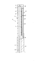
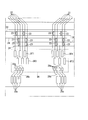
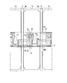
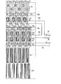
- FIG. 1 is a diagram for explaining a liquid crystal display device using an active matrix substrate according to the first embodiment of the present invention.
- FIG. 2 is a diagram for explaining the configuration of the liquid crystal panel shown in FIG.
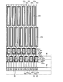
- FIG. 3 is a plan view for explaining the main part of the active matrix substrate.
- FIG. 4 is an enlarged plan view for explaining a mounting portion and its peripheral portion of the data driver shown in FIG.
- FIG. 5 is an enlarged plan view illustrating a pixel structure of the liquid crystal panel.
- 6 is a cross-sectional view taken along line VI-VI in FIG.
- FIG. 7 is a diagram for explaining a main configuration of the active matrix substrate shown in FIG.
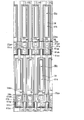
- FIG. 8 is an enlarged plan view for explaining the second thin film transistor and the first common wiring shown in FIG.
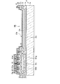
- FIG. 9 is a cross-sectional view taken along line IX-IX in FIG. 10 is a cross-sectional view taken along line XX of FIG.
- FIG. 11 is a cross-sectional view illustrating a second thin film transistor and a metal electrode on an active matrix substrate according to the second embodiment of the present invention.
- FIG. 12 is a plan view for explaining a main part of an active matrix substrate according to the third embodiment of the present invention.
- FIG. 13 is a diagram for explaining a main configuration of the active matrix substrate shown in FIG. 14 is a cross-sectional view taken along line XIV-XIV in FIG.
- FIG. 15 is a diagram for explaining a main part configuration on the side opposite to the data driver mounting part of the active matrix substrate shown in FIG. FIG.
- FIG. 16 is a plan view for explaining a main part of an active matrix substrate according to the fourth embodiment of the present invention.
- FIG. 17 is an enlarged plan view for explaining a mounting portion and its peripheral portion of the data driver shown in FIG.
- FIG. 18 is a diagram for explaining a main configuration of the active matrix substrate shown in FIG.
- FIG. 19 is an enlarged plan view for explaining the mounting terminal, the second thin film transistor, and the metal electrode shown in FIG. 20 is a cross-sectional view taken along line XX-XX in FIG. 21 is a cross-sectional view taken along line XXI-XXI in FIG.
- FIG. 1 is a diagram for explaining a liquid crystal display device using an active matrix substrate according to the first embodiment of the present invention.
- the liquid crystal display device 1 according to the present embodiment includes a liquid crystal panel 2 in which the upper side of FIG. 1 is installed as a viewing side (display surface side), and a non-display surface side of the liquid crystal panel 2 (lower side of FIG. 1). And a backlight device 3 that generates illumination light for illuminating the liquid crystal panel 2.
- the liquid crystal panel 2 includes a counter substrate 4 constituting the pair of substrates and the active matrix substrate 5 of the present invention, and polarizing plates 6 and 7 provided on the outer surfaces of the counter substrate 4 and the active matrix substrate 5, respectively. Yes. A liquid crystal layer described later is sandwiched between the counter substrate 4 and the active matrix substrate 5.
- the counter substrate 4 and the active matrix substrate 5 are made of a flat transparent glass material or a transparent synthetic resin such as an acrylic resin. Resin films such as TAC (triacetyl cellulose) or PVA (polyvinyl alcohol) are used for the polarizing plates 6 and 7 and correspond to cover at least the effective display area of the display surface provided in the liquid crystal panel 2. It is bonded to the counter substrate 4 or the active matrix substrate 5. In some cases, a ⁇ / 4 retardation plate (quarter wavelength plate) is disposed between the polarizing plates 6 and 7 and the liquid crystal layer.
- the active matrix substrate 5 constitutes one of the pair of substrates.
- pixel electrodes and thin film transistors thin film transistors (in accordance with a plurality of pixels included in the display surface of the liquid crystal panel 2) are provided.
- a TFT (Thin Film Transistor) or the like is formed between the liquid crystal layer (details will be described later).
- the counter substrate 4 constitutes the other substrate (counter substrate) of the pair of substrates, and a color filter, a counter electrode, and the like are formed between the liquid crystal layer and the counter substrate 4 ( Not shown).
- the liquid crystal panel 2 is provided with an FPC (Flexible Printed Circuit) 8 connected to a control device (not shown) for controlling the drive of the liquid crystal panel 2 and operates the liquid crystal layer in units of pixels.
- FPC Flexible Printed Circuit
- the display surface is driven in units of pixels and a desired image is displayed on the display surface.
- the liquid crystal mode and pixel structure of the liquid crystal panel 2 are arbitrary. Moreover, the drive mode of the liquid crystal panel 2 is also arbitrary. That is, as the liquid crystal panel 2, any liquid crystal panel that can display information can be used. Therefore, the detailed structure of the liquid crystal panel 2 is not shown in FIG.
- the backlight device 3 includes a light emitting diode 9 as a light source, and a light guide plate 10 disposed to face the light emitting diode 9.
- the light emitting diode 9 and the light guide plate 10 are sandwiched by the bezel 14 having an L-shaped cross section in a state where the liquid crystal panel 2 is installed above the light guide plate 10.
- a case 11 is placed on the counter substrate 4.
- the backlight device 3 is assembled to the liquid crystal panel 2 and is integrated as a transmissive liquid crystal display device 1 in which illumination light from the backlight device 3 is incident on the liquid crystal panel 2.
- the light guide plate 10 for example, a synthetic resin such as a transparent acrylic resin is used, and light from the light emitting diode 9 enters.
- a reflection sheet 12 is installed on the opposite side (opposite surface side) of the light guide plate 10 to the liquid crystal panel 2.
- an optical sheet 13 such as a lens sheet or a diffusion sheet is provided on the liquid crystal panel 2 side (light emitting surface side) of the light guide plate 10, and the inside of the light guide plate 10 has a predetermined light guide direction (left side in FIG. 1). The light from the light emitting diode 9 guided in the direction from the right side to the right side is changed to the planar illumination light having uniform luminance and applied to the liquid crystal panel 2.
- the present embodiment is not limited to this, and a direct type backlight device is used. May be.
- a backlight device having other light sources such as a cold cathode fluorescent tube and a hot cathode fluorescent tube other than the light emitting diode can also be used.
- liquid crystal panel 2 of the present embodiment will be specifically described with reference to FIG.
- FIG. 2 is a diagram for explaining the configuration of the liquid crystal panel shown in FIG.
- the liquid crystal display device 1 includes a panel control unit 15 that performs drive control of the liquid crystal panel 2 (FIG. 1) as the display unit that displays information such as characters and images, and the panel control.
- a data driver (source driver) 16 and a gate driver 17 that operate based on an instruction signal from the unit 15 are provided.
- the panel control unit 15 is provided in the control device, and receives a video signal from the outside of the liquid crystal display device 1. Further, the panel control unit 15 performs predetermined image processing on the input video signal to generate each instruction signal to the data driver 16 and the gate driver 17, and the input video signal. A frame buffer 15b capable of storing display data for one frame included. Then, the panel control unit 15 performs drive control of the data driver 16 and the gate driver 17 according to the input video signal, so that information corresponding to the video signal is displayed on the liquid crystal panel 2.
- the data driver 16 and the gate driver 17 are installed on the active matrix substrate 5. Specifically, the data driver 16 is installed on the surface of the active matrix substrate 5 along the lateral direction of the liquid crystal panel 2 in the outer region of the effective display area A of the liquid crystal panel 2 as a display panel. . Further, the gate driver 17 is installed on the surface of the active matrix substrate 5 so as to be along the vertical direction of the liquid crystal panel 2 in the outer region of the effective display region A. As described in detail later, the gate driver 17 may be divided into two gate drivers provided so as to sandwich the effective display area A, or the gate driver 17 may be the liquid crystal. You may arrange
- the data driver 16 and the gate driver 17 are driving circuits that drive a plurality of pixels P provided on the liquid crystal panel 2 side by pixel, and the data driver 16 and the gate driver 17 include a plurality of data bus lines ( Source wirings) D1 to DM (M is an integer of 2 or more, hereinafter collectively referred to as “D”) and a plurality of gate bus lines (gate wirings) G1 to GN (N is an integer of 2 or more; Are generally connected by "G").
- the data bus lines D and the gate bus lines G are arranged in a matrix so as to intersect each other on a transparent glass material or a transparent synthetic resin substrate described later included in the active matrix substrate 5. Yes.
- the data bus lines D are provided on the substrate so as to be parallel to the matrix column direction (vertical direction of the liquid crystal panel 2), and the gate bus lines G are arranged in the matrix row direction (the liquid crystal panel 2). In the horizontal direction) on the base material.
- a first thin film transistor 18 as a first switching element and a pixel electrode 19 connected to the first thin film transistor 18 are provided.
- the pixel P is provided.
- the counter electrode 20 is configured to face the pixel electrode 19 with the liquid crystal layer provided on the liquid crystal panel 2 interposed therebetween. That is, in the active matrix substrate 5, the first thin film transistor 18 and the pixel electrode 19 are provided for each pixel.
- regions of a plurality of pixels P are formed in regions partitioned by the data bus lines D and the gate bus lines G in a matrix.
- the plurality of pixels P include red (R), green (G), and blue (B) pixels.
- the RGB pixels are sequentially arranged in this order, for example, in parallel with the gate bus lines G1 to GN. Further, these RGB pixels can display corresponding colors by the color filter layer provided on the counter substrate 4 side.
- the gate driver 17 turns on the gate electrode of the corresponding first thin film transistor 18 for the gate bus lines G1 to GN based on the instruction signal from the image processing unit 15a. Scan signals (gate signals) are sequentially output.
- the data driver 16 applies data signals (voltage signals (gradation voltages)) corresponding to the luminance (gradation) of the display image based on the instruction signal from the image processing unit 15a to the corresponding data bus lines D1 to DM. Output to.
- FIG. 3 is a plan view for explaining the main part of the active matrix substrate.
- FIG. 4 is an enlarged plan view for explaining a mounting portion and its peripheral portion of the data driver shown in FIG.
- FIG. 5 is an enlarged plan view illustrating a pixel structure of the liquid crystal panel.
- 6 is a cross-sectional view taken along line VI-VI in FIG.
- FIG. 7 is a diagram for explaining a main configuration of the active matrix substrate shown in FIG.
- a plurality of data bus lines D and a plurality of gate bus lines G are arranged in a matrix in a portion covered with the counter substrate 4. Further, as shown by a one-dot chain line in FIG. 3, the effective display area A is provided.
- a plurality of gate bus lines G are formed in the gate layer, and a gate insulating film described later is provided so as to cover the gate bus lines G.
- a plurality of data buses are provided on the gate insulating film, that is, in the source layer.
- Line D is formed.
- the data bus line D and the gate bus line G are wirings provided in the effective display area A, respectively. Note that the points where the bus lines formed in the source layer and the bus lines formed in the gate layer are connected are indicated by black circles in FIG. 3 (also in FIGS. 12 and 16 described later).
- the bus line indicated by G (the bus line in the horizontal direction on the paper) is a data bus line
- the bus line indicated by D (the bus line in the vertical direction on the paper) is a gate bus line. Good.
- the gate drivers 17a and 17b are monolithically formed on the base material of the active matrix substrate 5 so as to sandwich the effective display area A.
- a plurality of gate bus lines G are alternately connected to these gate drivers 17a and 17b.
- the gate drivers 17a and 17b are connected to the gate driver driving signal terminal 21b via the gate driver driving signal wiring 21a.
- the gate driver driving signal terminal 21b is connected to the FPC connection terminal of the FPC 8.
- Each of the gate drivers 17a and 17b receives an FPC 8 as an instruction signal from the image processing unit 15a. It is supposed to be input after that.
- the gate drivers 17a and 17b may be connected to the same gate bus line G, or the gate driver may be provided only on one side with respect to the effective display area A.
- the structure which mounts the gate drivers 17a and 17b which consist of IC chips on the said base material may be sufficient.
- An auxiliary capacitance electrode CS for generating a predetermined auxiliary capacitance is provided for each pixel P on the base material of the active matrix substrate 5, and this auxiliary capacitance electrode CS is an auxiliary capacitance electrode drive signal.
- the storage capacitor electrode drive signal terminal CS2 is connected via the wiring CS1.
- the auxiliary capacitor electrode driving signal terminal CS2 is connected to the FPC connection terminal of the FPC 8 so that a voltage is supplied to the auxiliary capacitor electrode CS.
- the auxiliary capacitance electrode CS constitutes a common electrode, is made of a transparent electrode material, and is provided below the pixel electrode 19 (details will be described later).
- the data driver 16 is composed of, for example, an IC chip (driver chip), and is a portion of the base material 5a of the rectangular active matrix substrate 5 indicated by a dotted line DA in FIGS. 3 and 4 outside the effective display area A. In contrast, it has been implemented.
- the bumps are connected to mounting terminals DT1 and DT2 provided in, for example, a two-stage staggered arrangement, and input mounting terminals 28a provided on the FPC 8 side. It has become so.
- a second thin film transistor 23 as a second switching element provided for each data bus line D is connected to each of the mounting terminals DT1 and DT2.
- each of the plurality of second thin film transistors 23 a plurality of gate bus lines G and a plurality of data bus lines D are wired in a matrix, and a plurality of pixel electrodes 19 are arranged in a matrix. Is provided outside the effective display area A. Further, each second thin film transistor 23 is connected to a lead line 22 that connects the mounting terminal DT1 or DT2 and the data bus line D.
- a lead-out line 22 is also provided for each data bus line D. As shown in FIG. 3, the lead-out line 22 forms a fan-out portion (oblique portion) FA wired obliquely with respect to the data bus line D. Yes.
- the lead-out line 22 includes a fan-out portion FA arranged at an angle with respect to the direction in which the data bus line D is arranged (the vertical direction of the liquid crystal panel 2).
- the plurality of lead lines 22 of the fan-out portion FA may be arranged in parallel with each other, or may be arranged so that the interval between the lead-out lines 22 increases toward the data bus line D side.
- the shape of the lead line 22 in the fan-out portion FA is not limited to a linear shape, and may be, for example, a curved shape or a polygonal line shape.
- the two adjacent lead lines 22 are formed of different conductive layers.
- the input mounting terminal 28a is connected to the data driver driving signal terminal 28c via the data driver driving signal wiring 28b.
- the data driver driving signal terminal 28c is connected to the FPC connection terminal of the FPC 8.
- the data driver 16 receives an instruction signal from the image processing unit 15a via the FPC 8. It has become.
- the fan-out portion FA and the mounting terminals DT1 and DT2 it is common to at least a part of the second thin film transistor 23 and the plurality of second thin film transistors 23. At least a part of the first common wiring 24 to be connected is arranged. Specifically, between the fan-out portion FA and the mounting terminals DT1 and DT2, a plurality of the second thin film transistors 23, three first common wires 24, and a plurality of second thin film transistors 23 and 3 are provided. A connection wiring described later for connecting any one of the first common wirings 24 and a control line 26 for controlling the on / off operation of each of the plurality of second thin film transistors 23 are provided.
- Each of the second thin film transistors 23, the first common wiring 24, the connection wiring, and the control line 26 is used for inspection processing and electrostatic countermeasures for each of the plurality of data bus lines D, or for alignment processing of liquid crystal molecules in the liquid crystal layer. It is installed to perform predetermined operation processing such as voltage application processing performed at the time.
- each of the plurality of data bus lines D is, for example, for each RGB color, any one of the first common lines via the lead-out line 22, the second thin film transistor 23, and the connection wiring. It is connected to the wiring 24.
- Each first common wiring 24 is connected to a terminal 25a, and this terminal 25a is connected to an input terminal 25c via a wiring 25b.
- the FPC connection terminal of the FPC 8 is connected to the input terminal 25c.
- the inspection signal in the inspection process and the voltage in the voltage application process are input from the terminal 25a or the input terminal 25c. Further, in the final product of the liquid crystal display device 1, the input terminal 25c is grounded via the FPC 8.
- the lead-out line 22, the connection wiring, and the first common wiring 24 are provided for each RGB color, as will be described in detail later.
- the second thin film transistor 23 is provided for each color of RGB, and is divided into second thin film transistors 23r, 23g, and 23b (details will be described later).
- a terminal 27a is connected to the control line 26, and this terminal 27a is connected to an input terminal 27c via a wiring 27b.
- the FPC connection terminal of the FPC 8 is connected to the input terminal 27c.
- a gate bus line G (gate layer) on the base material 5 a and a first integrated with the gate bus line G are provided.
- a gate electrode 18g of the thin film transistor 18 is provided.
- the gate bus line G and the gate electrode 18g include a plurality of stacked metal films, for example, a copper film and a titanium film, a copper film and a molybdenum film, or a two-layer metal film such as a copper film and a molybdenum alloy film, Alternatively, a metal film having a three-layer structure such as an aluminum film, a titanium film, and an aluminum film, or a molybdenum film, an aluminum film, or a molybdenum film is used. In some cases, a molybdenum film, an aluminum film, a chromium film, or an alloy film thereof is used as a single layer.
- a gate insulating film 29 is provided so as to cover the base material 5a, the gate bus line G, and the gate electrode 18g.
- the gate insulating film 29 constitutes an insulating film.
- silicon nitride (SiNx), or a laminated film of silicon nitride (SiNx) and silicon oxide (SiO 2 ) is used. ing.
- the semiconductor layer 18 h of the first thin film transistor 18 is formed on the gate insulating film 29.
- an oxide semiconductor is used for the semiconductor layer 18h.
- an In—Ga—Zn—O-based amorphous oxide semiconductor containing In, Ga, and Zn at a ratio of 1: 1: 1 is preferably used.
- the ratio of In, G, and Zn is not limited to the above, and may be appropriately selected.
- another oxide semiconductor film can be used instead of the In—Ga—Zn—O-based oxide semiconductor film.
- the semiconductor layer 18h may be formed of an InGaO3 (ZnO) film, magnesium zinc oxide (MgxZn1-xO), cadmium zinc oxide (CdxZn1-xO), cadmium oxide (CdO), or the like.
- ZnO InGaO3
- MgxZn1-xO magnesium zinc oxide
- CdxZn1-xO cadmium zinc oxide
- CdO cadmium oxide
- ZnO may be formed using ZnO to which one or a plurality of impurity elements are added among a group 1 element, a group 13 element, a group 14 element, a group 15 element or a group 17 element.
- An impurity element may not be added to ZnO.
- ZnO may be in an amorphous state, a polycrystalline state, or a microcrystalline state in which an amorphous state and a polycrystalline state are mixed.
- An amorphous In—Ga—Zn—O-based oxide semiconductor can be manufactured at a low temperature and has an advantage that high mobility can be realized.
- an In—Ga—Zn—O-based oxide semiconductor having crystallinity may be used instead of the amorphous In—Ga—Zn—O-based oxide semiconductor.
- As the crystalline In—Ga—Zn—O-based oxide semiconductor layer a crystalline In—Ga—Zn—O-based oxide semiconductor layer in which the c-axis is oriented substantially perpendicular to the layer surface is preferable.
- a thin film transistor having such an In—Ga—Zn—O-based oxide semiconductor layer is described in, for example, Japanese Patent Application Laid-Open No. 2012-123475.
- the semiconductor layer 18h may be configured using, for example, amorphous silicon, polysilicon, or microcrystalline silicon.
- the channel protective layer 30 is provided on the gate insulating film 29 and the semiconductor layer 18h.
- silicon oxide (SiO 2 ) is used for the channel protective layer 30.
- the channel protective layer 30 is not an essential component and can be omitted.
- the data bus line D (source layer), the source electrode 18 s of the first thin film transistor 18 integrally formed with the data bus line D, and the drain of the first thin film transistor 18 are provided.
- An electrode 18d is provided.
- the data bus line D, the source electrode 18s, and the drain electrode 18d include a metal film having a two-layer structure such as a copper film and a titanium film, a copper film and a molybdenum film, or a copper film and a molybdenum alloy film, or an aluminum film.
- a metal film having a three-layer structure such as a titanium film and an aluminum film or a molybdenum film, an aluminum film, and a molybdenum film is used. In some cases, a molybdenum film, a chromium film, or an alloy film thereof is used as a single layer.
- Interlayer insulating films 31 and 32 are sequentially provided so as to cover the data bus line D, the source electrode 18s, and the drain electrode 18d.
- silicon nitride (SiNx) is used for the interlayer insulating film 31.
- a photosensitive organic film is used for the interlayer insulating film 32.
- auxiliary capacitance electrode CS is formed on the interlayer insulating film 32.
- a transparent electrode material such as ITO or IZO is used.
- the metal electrode 44 is provided so as to be in direct contact with the upper layer of the auxiliary capacitance electrode (common electrode) CS, so that the resistance of the auxiliary capacitance electrode CS is reduced. Further, the metal electrode 44 is configured to be used as a light-shielding film that covers at least a part of the second thin film transistor 23, as will be described in detail later.
- the metal electrode 44 is made of, for example, molybdenum, titanium, aluminum, or an alloy or laminated film thereof.
- a strip-shaped metal electrode 44 is provided so as to cover the first thin film transistor 18. That is, the metal electrode 44 has sides 44 a and 44 b facing each other, and includes an opening 44 c provided so as to surround a contact hole H ⁇ b> 1 described later, and is provided in parallel with the gate bus line G. As shown in FIG. 6, the metal electrode 44 is provided below the pixel electrode 19 and in an upper layer of the auxiliary capacitance electrode CS so as to be in direct contact with the auxiliary capacitance electrode CS. Further, as shown in FIG. 6, the metal electrode 44 is configured to cover at least a part of the first thin film transistor 18 (that is, a part excluding the drain electrode 18d around the contact hole H1). It is supposed to function as well.
- An interlayer insulating film 33 is provided so as to cover the interlayer insulating film 32, the auxiliary capacitance electrode CS, and the metal electrode 44.
- silicon nitride (SiNx) is used for the interlayer insulating film 33.
- an auxiliary capacitance is formed for each pixel P by overlapping the auxiliary capacitance electrode CS with a pixel electrode 19 described later via the interlayer insulating film 33.
- the pixel electrode 19 is formed on the interlayer insulating film 33.
- the pixel electrode 19 is made of a transparent electrode material such as ITO or IZO.
- the interlayer insulating films 32 and 33 are provided with openings, and the contact hole H1 for connecting the drain electrode 18d and the pixel electrode 19 to each other is formed.
- the liquid crystal panel 2 of the present embodiment is a so-called vertical electric field liquid crystal panel, and uses, for example, a pixel P of a CPA (Continuous Axis Alignment) mode which is a kind of vertical alignment mode.
- a vertical alignment film is provided on each inner surface of the active matrix substrate 5 and the counter substrate 4, and a liquid crystal having a negative dielectric anisotropy is formed between these vertical alignment films.
- the liquid crystal layer is provided.
- the counter substrate 4 is provided with the counter electrode 20 and an alignment control structure, for example, an alignment control protrusion CT (FIG. 5) between the counter electrode 20 for each pixel P and the vertical alignment film. Is provided.
- a notch may be provided for each pixel P in the counter electrode 20 as a structure for alignment control instead of the alignment control protrusion CT.
- the alignment direction of the liquid crystal is continuously varied within one pixel around the alignment control projection CT at the substantially central portion of the pixel P. That is, since the alignment control protrusion CT is provided in the substantially central portion of the pixel P, the liquid crystal molecules of the liquid crystal layer are radially emitted around the alignment control protrusion CT, that is, around the pixel central portion when a voltage is applied. Orient. In this way, by using the alignment control protrusion CT, liquid crystal molecules in the pixel P can be radially aligned when a voltage is applied, so that viewing angle characteristics can be improved.
- a PSA (Polymer Sustained Alignment) technique is applied to the pixel P of the present embodiment.
- This PSA technique is a technique of forming an alignment maintaining layer (Alignment Sustaining Layer) that gives a pretilt to the liquid crystal when no voltage is applied in order to regulate the alignment direction of liquid crystal molecules when no voltage is applied.
- This alignment maintaining layer is a polymer obtained by forming a liquid crystal cell and then photopolymerizing a photopolymerizable monomer (or oligomer) premixed in a liquid crystal material, typically with a voltage applied to the liquid crystal layer. Formed as a layer.
- the alignment maintaining layer maintains the liquid crystal when no voltage is applied to the pretilt angle in a direction slightly inclined (for example, 2 ° to 3 °) from the direction perpendicular to the substrate surface of the active matrix substrate 5 and the alignment direction (memory). Can be made. Thereby, the response speed of the liquid crystal alignment at the time of voltage application can be improved. Moreover, the return of the orientation when the surface of the liquid crystal panel 2 is pressed with a finger can be accelerated. That is, by implementing the PSA technique in combination with the pixel P in the CPA mode, it is possible to obtain the effect of improving the response speed and the speed of returning when the finger is pressed.
- voltage application for implementing this PSA technique is performed using the terminal 25a or the input terminal 25c described above. That is, the voltage is supplied to all the data bus lines D via the (input terminal 25c, wiring 25b) terminal 25a, the first common wiring 24, the connection wiring, the second thin film transistor 23, and the lead line 22. Is done. Further, by inputting a predetermined signal to the gate driver driving signal terminal 21b, the gate drivers 17a and 17b are driven, and a voltage for turning on the first thin film transistor 18 is supplied to the gate bus line G. As a result, the voltage supplied to the data bus line D is supplied to the liquid crystal layer via the first thin film transistor 18 to form the alignment maintaining layer.
- the counter substrate 4 is provided with a black matrix film BM so as to cover the data bus line D, the first thin film transistor 18, and the contact hole H ⁇ b> 1.
- a black matrix film BM is used as a countermeasure against color mixture when a bonding misalignment occurs between the active matrix substrate 5 and the counter substrate 4, or as a light shield for the channel portion of the first thin film transistor 18, or in the contact hole H1. It is provided as a countermeasure against deterioration in display quality due to disorder in the alignment of the liquid crystal.
- lead lines 22r, 22g, and 22b respectively corresponding to, for example, RGB colors are sequentially arranged along the horizontal direction of the drawing. .
- the lead wires 22r, 22g, and 22b are connected to the mounting terminals DT1 or DT2. Further, as shown in FIG. 7, the mounting terminals DT1 and DT2 are arranged in a two-stage staggered manner (that is, the two adjacent mounting terminals DT1 and DT2 are arranged at different positions in the linear direction). Are arranged sequentially shifted). Thereby, the plurality of mounting terminals DT1 and DT2 can be efficiently arranged, and the probability of occurrence of a short circuit in the vicinity of the two adjacent mounting terminals DT1 and DT2 can be reduced.
- bumps (electrodes) of the data driver 16 are connected to the mounting terminals DT1 and DT2. Note that bumps (electrodes) are connected to the mounting terminals DT1 and DT2, a terminal upper layer electrode formed of the same conductive layer as the pixel electrode 19, and a terminal connected to the terminal upper layer electrode, and a data bus line D The terminal lower layer electrode formed by the same conductive layer is provided (not shown).
- one of the plurality of lead lines 22r, 22g and 22b, one of the two lead lines 22 adjacent to each other is formed of the same conductive layer (gate layer) as the gate bus line G.
- Two other adjacent data bus line lead lines 22 are formed of the same conductive layer (source layer) as the data bus line D.
- two adjacent lead lines 22 are formed on the gate layer (first conductive layer) on the substrate 5a (FIG. 6), and the other two adjacent lead lines 22 are It is formed in the source layer (second conductive layer) above the gate insulating film 29 covering the gate layer.
- the gate layer is formed on the base material 5a (FIG. 6) by the same metal material (single layer or a plurality of kinds of laminated metal materials) and the same manufacturing process as the gate electrode 18g shown in FIG. is there.
- the source layer is formed above the base material 5a by the same metal material (single layer or a plurality of kinds of stacked metal materials) and the same manufacturing process as the source electrode 18s and the drain electrode 18d shown in FIG. It is a thing.
- the lead lines 22r, 22g, and 22b formed in the gate layer are connected from the gate layer to the source layer (the same as the data bus line D) in the switching unit 70. To the conductive layer).
- a gate layer lead line 22g (1) is formed on the base material 5a, and a gate insulating film is further formed on the base material 5a so as to cover the lead line 22g (1). 29 and a channel protective layer 30 are formed.
- a lead line 22 g (2) is formed on the gate insulating film 29 and the channel protective layer 30. Where the lead line 22g (1) and the lead line 22g (2) overlap each other, the lead line 22g (1) and the lead line 22g (2) are directly connected without the gate insulating film 29 and the channel protective layer 30 interposed therebetween. It comes to contact.
- an interlayer insulating film 31 is further formed so as to cover them.
- An interlayer insulating film 33 is further formed on the interlayer insulating film 31.
- An interlayer insulating film (photosensitive organic film) 32 may be formed between the interlayer insulating film 31 and the interlayer insulating film 33.
- the lead line 22g (1) and the lead line 22g (2) are formed so as to overlap with each other in the layer thickness direction in the connecting portion 70.
- the gate insulating film 29 and the channel protective layer 30 are removed in a part of the overlapping region, and the lead line 22g (1) is in contact with the lead line 22g (2).
- the wiring formed by the lead line 22g (1) in the gate layer is connected to the lead line 22g (2) in the source layer.
- lead lines 22r and 22b formed in the gate layer are also switched from the gate layer to the source layer via the switching unit 70, similarly to the lead line 22g described in FIG.
- the lead-out line 22 has a line width larger than that of the other part in the connecting part 70.
- the area of the connecting portion 70 is 19 ⁇ m ⁇ 19 ⁇ m, for example.
- two adjacent left and right lead lines 22 correspond to the part where the line width is thick in the connection part 70 of the lead line 22.
- the interval between the wirings 22b) is wide. In this way, by increasing the interval between adjacent wirings according to the line width of the wiring of the connection switching unit 70, the wiring can be efficiently arranged even in a region where a plurality of wirings are concentrated.
- reconnecting section 70 is arranged in a staggered manner with a position shifted with respect to another reconnecting section 70 adjacent via the lead wire 22.
- the some connection part 70 can be arrange
- the fan By connecting the lead line 22 formed in the gate layer from the gate layer to the source layer below the fan-out portion FA, that is, in the vicinity of the second thin film transistor (second switching element) 23, the fan It is possible to secure a long lead line 22 in a state separated into the gate layer and the source layer in the out part FA. For this reason, it is possible to reduce the probability that adjacent lead wires 22 are short-circuited.
- the lead lines 22r, 22g, and 22b are branch wirings of the control line 26 formed in the gate layer (first conductive layer). It is provided so as to be orthogonal to 26a or 26b. These branch wirings 26a or 26b are configured integrally with the gate electrodes 23rg, 23gg, and 23bg of the second thin film transistors 23r, 23g, and 23b, as will be described in detail later.
- each lead line 22 is connected to a first common wiring 24 formed in a gate layer (first conductive layer) through a second thin film transistor 23, respectively.
- the lead lines 22r, 22g, and 22b are connected to the second thin film transistors 23r, 23g, and 23b, the connection wiring 35r formed in the source layer (second conductive layer),
- the first common lines 24r, 24g, and 24b are connected to the first common lines 24r, 24g, and 24b through the terminal contact holes H2r, H2g, and H2b, respectively.
- a predetermined number of data bus lines D are connected to the first common lines 24r, 24g, and 24b via a predetermined number of second thin film transistors 23r, 23g, or 23b.
- each of the lead lines 22 formed of the same conductive layer as the gate bus lines G and the lead lines 22 formed of the same conductive layer as the data bus lines D are adjacent to each other.
- the two lead lines 22 are respectively connected to two first and second common wirings 24 provided differently from each other.
- the second lead line 22g from the right side of FIG. 7 and the fourth lead line 22r from the right side of FIG. 7 are both formed of the same conductive layer as the gate bus line G.
- the lead lines 22g and 22r are connected to different first common lines 24g and 24r.
- the first lead line 22r from the right side of FIG. 7 and the third lead line 22b from the right side of FIG. 7 are both formed of the same conductive layer as the data bus line D, but these lead lines 22r. And 22b are connected to different first common lines 24r and 24b.
- the branch wiring 26a of the control line 26 and the branch wiring 26a of the control line 26 are covered on the base material 5a of the active matrix substrate 5.
- a formed gate insulating film 29 is provided.
- the gate electrode 23 bg of the second thin film transistor 23 b is configured integrally with the branch wiring 26 a of the control line 26.
- the semiconductor layer 23bh and the channel protective layer 30 of the second thin film transistor 23b are sequentially stacked above the gate insulating film 29.
- the semiconductor layer 23bh is made of, for example, an oxide semiconductor, like the semiconductor layer 18h of the first thin film transistor 18.
- An interlayer insulating film 31 and an interlayer insulating film 33 are sequentially stacked on the drain electrode 23bd, the source electrode 23bs, and the channel protective layer 30.
- An interlayer insulating film (photosensitive organic film) 32 may be formed between the interlayer insulating film 31 and the interlayer insulating film 33.
- the configuration example of the second thin film transistor 23g is basically the same as that of the second thin film transistor 23b. Specifically, in the second thin film transistor 23g, the gate electrode 23gg is formed by the branch line 26b of the control line 26, the drain electrode 23gd is formed by the lead line 22g, and the source electrode 23gs is formed by the connection line 35g.
- the configuration example of the second thin film transistor 23r is a configuration in which the positions of the drain electrode 23bd and the source electrode 23bs in the second thin film transistor 23b are switched.
- the gate electrode 23rg is formed by the branch line 26b of the control line 26
- the drain electrode 23rd is formed by the lead line 22r
- the source electrode 23rs is formed by the connection line 35r.
- the four sides of the rectangular metal electrode 44 have the respective semiconductor layers 23rh, 23gh, and 23bh of the second thin film transistor 23r, 23g, and 23b. It is provided to surround.
- the electrode film CSa formed of the same conductive layer as the metal electrode 44 and the auxiliary capacitance electrode CS is formed of the interlayer insulating film 31 and the interlayer insulating film 33. It is provided between.
- the metal electrode 44 is provided above the gate electrode 23bg, the semiconductor layer 23bh, the drain electrode 23bd, and the source electrode 23bs of the second thin film transistor 23b, and functions as a light shielding film for them.
- the metal electrode (light-shielding film) 44 is covered with an interlayer insulating film 33.
- the metal electrode 44 completely covers the channel portions of the second thin film transistors 23r, 23g, and 23b when viewed from a direction perpendicular to the substrate surface of the active matrix substrate 5 from the viewpoint of suppressing leakage current described later. It is preferable to form.
- the lead line 22r includes a first common wiring 24b, a branch wiring 26a of the control line 26, a first common wiring 24g, a branch wiring 26b of the control line 26, and a first wiring.
- Width details 22ra, 22rb, 22rc, 22rd, and 22re each having a narrow width dimension are provided at a portion that intersects one common wiring 24r.
- the lead line 22r, the first common line 24b, the branch line 26a of the control line 26, the first common line 24g, and the control line The crossing areas of the 26 branch wirings 26b and the first common wiring 24r can be suppressed.
- signal delay on the data bus line D can be suppressed, and deterioration of display quality after chip mounting of the data driver 16 (that is, the final product of the liquid crystal display device 1) is prevented. be able to.
- the delay of the inspection control signal with respect to the control line 26 can be suppressed at the time of inspection, display unevenness can be easily reduced when inspection display is performed, and erroneous detection of defects can be suppressed. Can do.
- each width dimension of the first common wiring 24b, the branch wiring 26a of the control line 26, the first common wiring 24g, the branch wiring 26b of the control line 26, or the first common wiring 24r may be reduced by reducing the size of the lead wire 22r.
- a signal for turning off the second thin film transistor (second switching element) 23 may be input to the control line 26 via the FPC connection terminal 27c.
- the second thin film transistor 23 can be reliably turned off, and the display quality (eg, shadowing) of the final product can be prevented from being deteriorated.
- the metal electrode 44 is provided below the pixel electrode 19. Further, at least a part of each of the plurality of second thin film transistors (second switching elements) 23 is covered with a light shielding film formed of the metal electrode 44, and the metal electrode (light shielding film) 44 is formed of an interlayer insulating film. 33.
- the active matrix substrate 5 unlike the conventional example, it is possible to configure the active matrix substrate 5 at a low cost that can easily protect the second thin film transistor 23 without increasing the number of manufacturing steps.
- the metal electrode 44 of each pixel P in the display unit is used as the light shielding film of the second thin film transistor 23, and the interlayer insulating film 33 of each pixel P is used for the light shielding. Since it is used as a protective film for the film, the second thin film transistor 23 can be easily protected by reliably forming the light shielding film of the second thin film transistor 23 without increasing the number of manufacturing steps.
- the second thin film transistor 23 is covered with the light shielding film formed by the metal electrode 44, an inspection operation using the second thin film transistor 23 can be performed with high accuracy.
- the light shielding film can reduce the influence of the inspection environment on the display at the time of inspection, and suppress erroneous determination at the time of inspection. Specifically, it is possible to prevent external light from entering the second thin film transistor 23 and causing leakage current. Furthermore, since it functions as a light shielding film, it is not necessary to cover the second thin film transistor 23 with a highly light-shielding resin or tape, or with a bezel.
- each of the plurality of second thin film transistors 23 is provided outside the effective display area A provided so that the gate bus line G and the data bus line D intersect. Accordingly, in the present embodiment, the second thin film transistor 23 can be used to appropriately perform operation processing such as inspection processing and voltage application processing on the data bus line D.
- the metal electrode 44 is provided on the upper layer of the auxiliary capacitance electrode (common electrode) CS, display defects can be suppressed. That is, the auxiliary capacitance electrode CS is formed of a transparent electrode material such as ITO or IZO, but such ITO or IZO generally has a high resistance, and particularly when the display area is large, a signal to the auxiliary capacitance electrode CS. Display defects such as flicker and shadowing may occur due to the delay of (voltage signal). For this reason, in this embodiment, by stacking the metal electrode 44 on the auxiliary capacitance electrode CS, the resistance can be reduced and the occurrence of the display defect can be suppressed.
- the auxiliary capacitance electrode CS is formed of a transparent electrode material such as ITO or IZO, but such ITO or IZO generally has a high resistance, and particularly when the display area is large, a signal to the auxiliary capacitance electrode CS. Display defects such as flicker and shadowing may occur due to the delay of (voltage signal).
- the lead-out line 22 includes a fan-out portion FA that is arranged at an angle with respect to the direction in which the data bus line D is arranged.
- at least a part of the first common wiring 24 and at least a part of the second thin film transistor 23 are respectively disposed between the fan-out portion FA and the mounting terminals DT1 and DT2.
- first common wires 24r, 24g, and 24b are provided, and each of the first common wires 24r, 24g, and 24b includes a predetermined number of second thin film transistors 23r, A predetermined number of data bus lines D are connected via 23g or 23b. Accordingly, in the present embodiment, operation processing such as inspection processing and voltage application processing is performed on the data bus line D every predetermined number using the first common wirings 24r, 24g, and 24b. it can.
- one of the two adjacent lead lines 22 is formed of the same conductive layer as the gate bus line G, and the two other lead lines 22 adjacent to each other are It is formed of the same conductive layer as the data bus line D.
- the lead line 22 formed of the same conductive layer as the gate bus line G and the lead line 22 formed of the same conductive layer as the data bus line D two adjacent lead lines 22 are formed. Are respectively connected to two first and second common wirings 24 provided differently from each other. Accordingly, in the present embodiment, the first common wiring 24 is connected to each of the lead line 22 formed of the same conductive layer as the gate bus line G and the lead line 22 formed of the same conductive layer as the data bus line D. By using it, it is possible to easily perform an inspection operation as to whether or not a short circuit has occurred.
- an oxide semiconductor is used for the semiconductor layers 18h, 23ah, and 23bh.
- the high-performance and compact first and second thin film transistors 18, 23a, and 23b can be easily configured, and the first and second thin film transistors 18, 23a, and 23b can be formed.
- the used inspection operation can be performed with high accuracy.
- the active matrix substrate 5 which is inexpensive and can easily protect the second thin film transistor (second switching element) 23 without increasing the number of manufacturing steps is used, the cost is reduced.
- a high-performance liquid crystal display device (display device) 1 that is inexpensive and has a simplified manufacturing process can be easily configured.
- FIG. 11 is a cross-sectional view illustrating a second thin film transistor and a metal electrode on an active matrix substrate according to the second embodiment of the present invention.
- the main difference between the present embodiment and the first embodiment is that a metal electrode is provided below the storage capacitor electrode (common electrode).
- a metal electrode is provided below the storage capacitor electrode (common electrode).
- symbol is attached
- the metal electrode 44 and the electrode film CSa of the auxiliary capacitance electrode (common electrode) CS are formed on the interlayer insulating film 31 in this order. Yes.
- the metal electrode 44 is configured to cover at least a part of the second thin film transistor 23b (the channel portion of the second thin film transistor 23), as in the first embodiment. Also, it functions as a light shielding film.
- the electrode film CSa laminated on the upper side of the metal electrode 44 is configured to function also as a protective layer of the metal electrode 44, and the first example illustrated in FIG. Unlike the first embodiment, the installation of the interlayer insulating film 33 is omitted.
- the metal electrode 44 and the auxiliary capacitance electrode CS are provided below the pixel electrode 19 in the pixel portion where the pixel P is provided, as in the first embodiment.
- the metal electrode 44 and the auxiliary capacitance electrode CS may be provided above the pixel electrode 19 (not shown).
- the configuration in which the metal electrode 44 is provided above the pixel electrode 19 is such that, for example, in a liquid crystal panel in a horizontal alignment mode, the counter electrode as a common electrode (Not shown). At this time, slits parallel to each other are formed in the counter electrode as the common electrode, and a lateral electric field is generated between the counter electrode.
- the present embodiment can achieve the same operations and effects as the first embodiment.
- FIG. 12 is a plan view for explaining a main part of an active matrix substrate according to the third embodiment of the present invention.
- FIG. 13 is a diagram for explaining a main configuration of the active matrix substrate shown in FIG. 14 is a cross-sectional view taken along line XIV-XIV in FIG.
- FIG. 15 is a diagram for explaining a main part configuration on the side opposite to the data driver mounting part of the active matrix substrate shown in FIG.
- the main difference between the present embodiment and the first embodiment is that a third thin film transistor is provided at the end of the data bus line on the side to which no mounting terminal is connected, and a plurality of third thin film transistors are provided.
- the second common wiring connected in common to the thin film transistors is provided.
- symbol is attached
- the mounting terminal DT3 or DT4 is first connected to the lead line 22 in the mounting portion (shown by “DA” in the figure) where the data driver 16 is mounted. ing.
- the second thin film transistor (second switching element) 45 is connected to the mounting terminal DT 3 or DT 4, and all the second thin film transistors 45 are connected to one first common wiring 47.
- the mounting portion is provided with a control line 46 for controlling the on / off operation of each of the plurality of second thin film transistors 45.
- the active matrix substrate 5 of the present embodiment with respect to the data bus line D, on the data driver 16 (driver chip) side, the lead line 22, the mounting terminal DT3 or DT4, the second thin film transistor 45, A connection wiring described later and one first common wiring 47 are sequentially connected. Further, a terminal 49a is connected to the first common wiring 47, and this terminal 49a is connected to the input terminal 49c via the wiring 49b. Further, the FPC connection terminal of the FPC 8 is connected to the input terminal 49c. The inspection signal for the data bus line D in the inspection process and the voltage in the voltage application process are input from the terminal 49a or the input terminal 49c. In the final product of the liquid crystal display device 1, the input terminal 49 c is grounded via the FPC 8.
- lead lines 22r, 22g, and 22b are provided for each color of RGB, for example, as in the first embodiment.
- the lead lines 22r, 22g, and 22b are connected to the RGB data bus line D, respectively.
- the mounting terminals DT3 or DT4 and the second thin film transistors 45a or 45b are sequentially connected to the lead lines 22r, 22g, and 22b.
- any of the connection wirings 50r, 50g, and 50b provided for each of RGB is connected to the second thin film transistor 45a or 45b.
- the first common wiring 47 is connected to the connection wirings 50r, 50g, and 50b through the terminal contact hole H3.
- the connection wirings 50r, 50g, and 50b are formed of the same conductive layer (source layer) as the data bus line D, and the first common wiring 47 is formed of the same conductive layer (gate layer) as the gate bus line G. Has been.
- the bumps (electrodes) of the data driver 16 are connected to the mounting terminals DT3 and DT4 as in the first embodiment.
- bumps (electrodes) are connected to the mounting terminals DT3 and DT4, and a terminal upper layer electrode formed of the same conductive layer as the pixel electrode 19 and the terminal upper layer electrode
- two terminal lower layer electrodes respectively formed by the same conductive layer as the data bus line D and the same conductive layer as the gate bus line G are provided (not shown).
- the mounting terminal DT3 is provided with the function of the switching unit 70, and the first terminal lower layer electrode (leading line 22) formed of the same conductive layer as the gate bus line G is connected to the data bus line D.
- the second terminal lower layer electrode (the drain electrode of the second thin film transistor) formed of the same conductive layer is connected to be connected to the second thin film transistor 45. That is, the mounting terminals DT3 and DT4 have the same configuration of the terminal upper layer electrode and the terminal lower layer electrode as the mounting terminals DT5 and DT6 in the fourth embodiment described later (see FIGS. 20 and 21). ).
- the second thin film transistors 45a and 45b are configured in the same manner as the second thin film transistor 23b shown in FIG. That is, as illustrated in FIG. 14, in the vicinity of the second thin film transistor 45 b, the control line 46 and the gate insulating film 29 formed so as to cover the control line 46 are formed on the base material 5 a of the active matrix substrate 5. Is provided. Further, the gate electrode 45 bg of the second thin film transistor 45 b is configured integrally with the control line 46.
- the semiconductor layer 45bh and the channel protective layer 30 of the second thin film transistor 45b are sequentially stacked above the gate insulating film 29.
- the semiconductor layer 45bh is made of, for example, an oxide semiconductor, like the semiconductor layer 18h of the first thin film transistor 18.
- An interlayer insulating film 31 and an interlayer insulating film 33 are sequentially stacked on the drain electrode 45bd, the source electrode 45bs, and the channel protective layer 30.
- the second thin film transistor 45 four sides of the rectangular metal electrode 44 are provided so as to surround the semiconductor layers 45ah and 45bh of the second thin film transistors 45a and 45b.
- the electrode film CSa formed of the same conductive layer as the metal electrode 44 and the auxiliary capacitance electrode CS is formed of the interlayer insulating film 31, the interlayer insulating film 33, and the like. It is provided between.
- the metal electrode 44 is provided above the gate electrode 45bg, the semiconductor layer 45bh, the drain electrode 45bd, and the source electrode 45bs of the second thin film transistor 45b, and functions as a light shielding film for them.
- the metal electrode (light-shielding film) 44 is covered with an interlayer insulating film 33.
- the metal electrode 44 is formed so as to completely cover the channel portions of the second thin film transistors 45a and 45b when viewed from a direction perpendicular to the substrate surface of the active matrix substrate 5 from the viewpoint of suppressing leakage current described later. It is preferable.
- the ON / OFF operation of each of the plurality of second thin film transistors 45 is controlled by a control line 46.
- the control line 46 has a terminal 48a.
- the terminal 48a is connected to the input terminal 48c via the wiring 48b.
- the FPC connection terminal of the FPC 8 is connected to the input terminal 48c.
- a control signal for performing the on / off operation of each second thin film transistor 45 is input from the terminal 48a or the input terminal 48c.
- a signal for turning off each second thin film transistor 45 is input to the input terminal 48c via the FPC 8.
- the end on the side to which the mounting terminal DT3 or DT4 is not connected is led out of the effective display area A by a plurality of lead lines 51.
- a third thin film transistor 52 as a third switching element and a connection wiring 53 are sequentially connected to each of the plurality of lead lines 51.
- the plurality of connection wirings 53 are connected to any one of the three second common wirings 54.
- the ON / OFF operation of the third thin film transistor 52 is controlled by the control line 56. That is, in the third thin film transistor 52, the gate electrode (not shown) is integrally formed with the control line 56. Further, a terminal 57 is connected to the control line 56, and this terminal 57 is connected to an input terminal 58 through a wiring. The input terminal 58 is connected to the FPC connection terminal of the FPC 8.
- a control signal for performing the on / off operation of the third thin film transistor 52 is input from the terminal 57 or the input terminal 58.
- a signal for turning off each third thin film transistor 52 is input to the input terminal 58 via the FPC 8.
- each second common wiring 54 is connected to a terminal 55 through a wiring, and an inspection signal, a voltage, and the like in the inspection processing for the data bus line D are supplied to the terminal 55. It has become.
- lead lines 51r, 51g, and 51b are provided for each of RGB colors.
- the lead lines 51r, 51g, and 51b are connected to the non-input side ends of the RGB data bus lines D, respectively.
- a drain electrode (not shown) of the third thin film transistor 52 is connected to each of the lead lines 51r, 51g, and 51b.
- any of the second common wirings 54r, 54g, and 54b provided for each of the RGB colors is connected to the source electrode (not shown) of the third thin film transistor 52 through the connection wiring 53 (FIG. 22).
- the corresponding lead lines 51r, 51g, and 51b are connected via the third thin film transistor 52 for each of the RGB colors.
- the inspection operation of the data bus line D can be performed for each color of RGB.
- the active matrix substrate 5 of this embodiment only one first common wiring 47 is provided on the input side of the data bus line D (that is, the driver chip mounting portion side). For this reason, in the inspection operation using the first common wiring 47, it is possible to detect the disconnection of each of the data bus line D and the lead-out line 22, the defect of the first thin film transistor 18, and the like.
- RGB single color display cannot be performed, and a short circuit between adjacent data bus lines D or adjacent lead lines 22 cannot be detected.
- the first common wires 54r, 54g, and 54b provided for each of RGB are provided on the non-input side of the data bus line D, thereby providing the first Similar to the embodiment, it is configured such that RGB single color display can be performed, and a short circuit between adjacent data bus lines D or adjacent lead lines 22 can be detected. Note that the disconnection of the lead wire 22 cannot be detected by the inspection using the second common wirings 54r, 54g, and 54b. Therefore, it is preferable to carry out in combination with the inspection using the first common wiring 47.
- the second common wirings 54r and 54g are used in the liquid crystal layer alignment process (voltage application process for implementing the PSA technique).
- And 54b can also be applied, and by applying voltage simultaneously from the first common wiring 47, the time required for the alignment process can be reduced. .
- the present embodiment can achieve the same operations and effects as the first embodiment.
- the third thin film transistor (third switching element) 52 connected to the end of the data bus line D to which the mounting terminal DT3 or DT4 is not connected, and a plurality of third thin films A second common wiring 54 connected in common to the thin film transistor 52 is provided. Accordingly, in the present embodiment, the configuration on the mounting terminal DT3 or DT4 side such as the configuration of the first common wiring 47 can be simplified, and even if the mounting area of the driver is small, the second thin film transistor (first 2 switching elements) 45 can be arranged more easily. Furthermore, in this embodiment, the driver mounting area can be narrowed.
- the outer dimensions of the active matrix substrate 5 and thus the liquid crystal display device 1 can be further reduced.
- the auxiliary capacitance electrode driving signal wiring CS1 of the auxiliary capacitance electrode (common electrode) CS is enlarged, that is, the auxiliary capacitance electrode driving signal wiring CS1 is made thicker, and the auxiliary capacitance electrode driving signal wiring is increased.
- the resistance of CS1 can be reduced. As a result, it is possible to suppress the occurrence of display defects such as flicker and shadowing due to the delay of the signal (voltage signal) to the auxiliary capacitance electrode CS.
- FIG. 16 is a plan view for explaining a main part of an active matrix substrate according to the fourth embodiment of the present invention.
- FIG. 17 is an enlarged plan view for explaining a mounting portion and its peripheral portion of the data driver shown in FIG.
- FIG. 18 is a diagram for explaining a main configuration of the active matrix substrate shown in FIG.
- FIG. 19 is an enlarged plan view for explaining the mounting terminal, the second thin film transistor, and the metal electrode shown in FIG. 20 is a cross-sectional view taken along line XX-XX in FIG. 21 is a cross-sectional view taken along line XXI-XXI in FIG.
- the main difference between the present embodiment and the first embodiment is that a second thin film transistor is disposed between the first common wiring and a terminal contact hole provided in the mounting terminal, and the mounting is performed.
- the terminal upper layer electrode of the terminal is provided so as to cover at least a part of the second thin film transistor.
- symbol is attached
- the active matrix substrate 5 of the present embodiment is provided with a mounting portion (indicated by “DA” in the drawing) on which the data driver 16 is mounted.
- a mounting terminal DT5 or DT6 provided continuously with the second thin film transistor 61 as the second switching element is provided.
- the mounting portion includes a plurality of second thin film transistors 61, three first common wires 24, a plurality of second thin film transistors 61, and any one of the three first common wires 24.
- a connection wiring 35 to be connected and a control line 26 for controlling the on / off operation of each of the plurality of second thin film transistors 61 are provided.
- Each of the second thin film transistors 61, the first common wiring 24, the connection wiring 35, and the control line 26 are used for inspection processing and electrostatic countermeasures for each of the plurality of data bus lines D, or alignment processing of liquid crystal molecules in the liquid crystal layer. It is installed to perform a predetermined operation process such as a voltage application process performed at the time.
- the active matrix substrate 5 of the present embodiment is provided with lead lines 22r, 22g, and 22b for each color of RGB, for example, as in the first embodiment. It has been.
- the lead lines 22r, 22g, and 22b are connected to the RGB data bus line D, respectively.
- the lead terminals 22r, 22g, and 22b are connected to the mounting terminals DT5 or DT6 through terminal contact holes H4a or H4b, respectively.
- the second thin film transistors 61a or 61b are connected to the mounting terminals DT5 or DT6, respectively.
- one of the connection wirings 35r, 35g, and 35b provided for each of RGB is connected to the second thin film transistor 61a or 61b.
- the first common wirings 24r, 24g, and 24b provided for each RGB are connected to the connection wirings 35r, 35g, and 35b through the terminal contact holes H5r, H5g, and H5b, respectively.
- the RGB data bus line D is connected to the first common wirings 24r, 24g, and 24b for each RGB color, and different inspections are performed for each RGB data bus line D. Signals can be input so that independent inspection operations can be performed.
- a predetermined number of RGB data bus lines D are predetermined on the first common wirings 24r, 24g, and 24b, as in the first embodiment.
- a plurality of second thin film transistors 61a or 61b are connected to each other and configured to be able to perform independent inspection operations for each of the RGB data bus lines D, so that a defect is visually detected.
- RGB single color display can be performed, and the leakage of the data bus line D can be easily detected.
- the second thin film transistor 61a continuously formed with the mounting terminal DT5 and the second thin film transistor 61b continuously formed with the mounting terminal DT6 are two-stage staggered.
- the two mounting terminals DT5 and DT6 that are adjacent to each other are sequentially shifted so as to be arranged at different positions in the linear direction.
- one of the two adjacent lead lines 22 is formed of the same conductive layer as the gate bus line G, and the other two lead lines 22 adjacent to each other are connected to the data bus. It is formed of the same conductive layer as the line D (see FIGS. 20 and 21).
- the lead line 22r is formed of the same conductive layer as the gate bus line G on the base material 5a.
- the gate electrode 61ag is formed on the substrate 5a.
- the gate electrode 61ag is integrally formed with the branch wiring 26a (FIG. 18) of the control line 26 formed of the same conductive layer as the gate bus line G.
- the end portion of the lead wire 22r is used as the first terminal lower layer electrode 36a of the mounting terminal DT5.
- the mounting terminal DT5 is provided with a second terminal lower layer electrode 36b formed of the same conductive layer as the data bus line D and a terminal upper layer electrode 34 formed of the same conductive layer as the pixel electrode 19. .
- the first terminal lower layer electrode 36a and the second terminal electrode H2a are formed through the terminal contact hole H4a formed in the gate insulating film 29, the channel protective layer 30, and the interlayer insulating films 31 and 33.
- the terminal lower layer electrode 36b is connected to each other, and the second terminal lower layer electrode 36b and the terminal upper layer electrode 34 are connected to each other.
- the second terminal lower layer electrode 36b is formed integrally with the drain electrode 61ad of the second thin film transistor 61a.
- the source electrode 61as is formed of the same conductive layer as the data bus line D, like the drain electrode 61ad. Further, as illustrated in FIG. , Constituting the end of the connection wiring 35r.
- the semiconductor layer 61ah is made of, for example, an oxide semiconductor, like the semiconductor layer 18h of the first thin film transistor 18.
- the terminal upper layer electrode 34 of the mounting terminal DT5 is formed so as to cover at least a part of the second thin film transistor 61a, and the bump (electrode) of the data driver 16 is connected to the terminal upper layer electrode 34. It is like that.
- a third terminal lower layer electrode 37a formed of the same conductive layer as the gate bus line G is provided on the base material 5a.
- the gate electrode 61bg is formed on the base material 5a.
- the gate electrode 61bg is integrally formed with the branch wiring 26b (FIG. 18) of the control line 26 formed of the same conductive layer as the gate bus line G.
- a part (end) of the lead line 22r formed of the same conductive layer as the data bus line D is used as the fourth terminal lower layer electrode 37b of the mounting terminal DT6.
- the mounting terminal DT6 is provided with a terminal upper layer electrode 34 formed of the same conductive layer as the pixel electrode 19.
- the third terminal lower layer electrode 37a and the fourth terminal electrode Ha are formed through the terminal contact hole H4b formed in the gate insulating film 29, the channel protective layer 30, and the interlayer insulating films 31 and 33.
- the terminal lower layer electrode 37b is connected to each other, and the fourth terminal lower layer electrode 37b and the terminal upper layer electrode 34 are connected to each other.
- the second terminal lower layer electrode 37b is formed integrally with the drain electrode 61bd of the second thin film transistor 61b. Further, in the second thin film transistor 61b, the source electrode 61bs is formed of the same conductive layer as the data bus line D, like the drain electrode 61bd. Furthermore, as illustrated in FIG. , Constituting the end of the connection wiring 35r.
- the semiconductor layer 61bh is made of, for example, an oxide semiconductor, similarly to the semiconductor layer 18h of the first thin film transistor 18.
- the terminal upper layer electrode 34 of the mounting terminal DT6 is formed so as to cover at least a part of the second thin film transistor 61b, and the bump (electrode) of the data driver 16 is connected to the terminal upper layer electrode 34. It is like that.
- width details 22ra, 22ga, and 22ba that are formed with narrow widths are formed at the intersections of the control line 26 and the branch wiring 26a, respectively. Is provided.
- connection wirings 35r, 35g, and 35b width details 35ra, 35ga, and 35ba each having a narrow width dimension are provided at the intersections of the control line 26 and the branch wiring 26b.
- the crossing areas of the branch wiring 26a and the lead lines 22r, 22g, and 22b, and the branch wiring 26b are provided. And the crossing areas of the connection wirings 35r, 35g, and 35b can be suppressed.
- signal delay on the data bus line D can be suppressed, and deterioration of display quality after chip mounting of the data driver 16 (that is, the final product of the liquid crystal display device 1) is prevented. be able to.
- the delay of the inspection control signal with respect to the control line 26 can be suppressed at the time of inspection, display unevenness can be easily reduced when inspection display is performed, and erroneous detection of defects can be suppressed. Can do.
- each branch wiring 26a and 26b of the control line 26 may be reduced to reduce the intersection area between the corresponding lead line 22 and the connection wiring 35.
- at the intersection at least one of the lead line 22, the connection wiring 35, and the branch wirings 26a and 26b may be thinned.
- the second thin film transistors 61a and 61b are in an off state. Thereby, in the final product of the liquid crystal display device 1, it is possible to prevent the display quality from being deteriorated (shadowing).
- the present embodiment can achieve the same operations and effects as the first embodiment.
- the terminal upper layer electrode 34 and the first and second terminal lower layer electrodes 36a and 36b are connected via the terminal contact hole H4a.
- the terminal upper layer electrode 34 and the third and fourth terminal lower layer electrodes 37a and 37b are connected via the terminal contact hole H4b.
- a second thin film transistor (second switching element) 61a is disposed between the first common wiring 24 and the terminal contact hole H4a, and a second thin film transistor (second switching element) 61b is disposed in the first common line. Arranged between the wiring 24 and the terminal contact hole H4b.
- the terminal upper layer electrode 34 is provided so as to cover at least a part of the second thin film transistor 61a or 61b.
- the connection area of the terminal upper layer electrode 34 and the driver chip (the bump) of the data driver 16 is not reduced, it is possible to suppress the occurrence of connection failure. Therefore, in the active matrix substrate 5 of the present embodiment, the second thin film transistors 61a and 61b can be easily arranged even when the mounting area of the data driver 16 is small.
- the arrangement region of the second thin film transistors 61a and 61b can be reduced in this way, the outer dimensions of the active matrix substrate 5, and thus the liquid crystal display device 1, can be easily reduced.
- the first terminal lower layer electrode 36a constituted by the end portion of the lead line formed of the same conductive layer as the gate bus line G, and the drain electrode of the second thin film transistor 61a
- a second terminal lower layer electrode 36b formed of the same conductive layer as the data bus line D is included.
- the first and second terminal lower layer electrodes 36a and 36b are connected to each other.
- the lead line 22 formed of the same conductive layer as the gate bus line G and the connection between the drain electrode 61ad of the second thin film transistor 61a formed of the same conductive layer as the data bus line D are switched.
- Can be performed in the terminal contact hole H4a and it is possible to omit installation of the region for reconnection (reconnection portion 70), and to easily reduce the outer dimensions of the active matrix substrate 5. Can do.
- the mounting terminal DT6 in the mounting terminal DT6, the third terminal lower layer electrode 37a formed of the same conductive layer as the gate bus line G and the end of the lead line 22 formed of the same conductive layer as the data bus line D are provided. And a fourth terminal lower layer electrode 37b integrally formed with the drain electrode 61bd of the second thin film transistor 61b. Further, in the terminal contact hole H4b, the third and fourth terminal lower layer electrodes 37a and 37b are connected to each other.
- the mounting terminals DT5 and DT6 can all have the same configuration regardless of the configuration of the lead wire 22, and the mounting state of the data driver (driver) 16 on the mounting terminals DT5 and DT6. Can be easily inspected.
- the driver chip of the data driver 16 and the mounting terminals DT5 or DT6 are connected through an anisotropic conductive film (ACF).
- ACF anisotropic conductive film
- indentation inspection of conductive particles contained in the conductive layer is performed. This indentation inspection is performed by observing the uneven shape formed on the mounting terminal DT5 or DT6 by the conductive particles from the back surface of the active matrix substrate 5, and conducting particles between the driver chip (the bumps) and the mounting terminals DT5 or DT6
- the film configurations of the mounting terminals DT5 and DT6 are the same. It is possible to prevent such a problem from occurring.
- two terminal contact holes may be provided in the mounting terminal DT5 or DT6.
- poor contact between the mounting terminal DT5 or DT6 and the data driver 16 can be easily reduced.
- the mounting terminal DT5 or DT6 portion of the terminal upper layer electrode 34 and the second thin film transistor 61a or 61b of the terminal upper layer electrode 34 can be provided compared to the fourth embodiment.
- the level difference from the covered portion can be reduced.
- the contact failure at the time of mounting the bump (electrode) of the driver chip of the data driver 16 can be reduced.
- the mounting terminals DT5 and DT6 in the fourth embodiment since the areas of the terminal contact holes H4a and H4b are large, it is possible to reduce the formation defects of the terminal contact holes H4a and H4b.
- the active matrix substrate of the present invention is not limited to this, and an effective display area having a plurality of pixels and
- the active matrix substrate of the present invention can be applied to any display device having a wiring for transmitting a signal for driving a pixel.
- the present invention can be applied to an organic EL display, a microcapsule-type electrophoresis display device, and other display devices.
- a microcapsule-type electrophoresis display device can be configured to display an image, for example, by applying a voltage to each microcapsule layer formed in an effective display region for each pixel.
- the display device includes, for example, a substrate including a wiring of an effective display region connected to a pixel electrode provided for each pixel via a switching element, and a lead line connected to the wiring of the effective display region.
- this substrate can be configured like the active matrix substrate in the above embodiment.
- the active matrix substrate of the present invention can be applied to various sensor substrates such as a sensor substrate for an X-ray detection device.
- the active matrix substrate of the present invention has the gate bus line G and the data
- the bus line D may be provided in a different layer via an insulating film
- the gate bus line G may be provided on the data bus line D via an insulating film.
- the configuration in which the mounting terminals DT are arranged in a two-stage staggered arrangement has been described.
- the active matrix substrate of the present invention is not limited to this.
- the mounting terminals DT are arranged in a three-stage staggered arrangement. (In other words, three adjacent mounting terminals DT may be sequentially shifted so as to be arranged at different positions in the linear direction.)
- the present invention is applied to a CPA mode liquid crystal panel (so-called vertical electric field liquid crystal panel) which is a kind of vertical alignment mode has been described.
- the active matrix substrate of the present invention is limited to this.
- the present invention can also be applied to other vertical alignment mode liquid crystal panels using fishbone type pixel electrodes and horizontal alignment mode liquid crystal panels (so-called horizontal electric field liquid crystal panels).
- the fishbone type pixel electrode can be represented by an azimuth angle that takes a positive angle counterclockwise with the right direction in the horizontal direction (direction in which the gate bus line extends) being 0 °, for example, 45 °, 135 °.
- a plurality of elongated electrode portions branches) extending at 225 °, 315 °, and 315 °, respectively. Between the elongated electrode portions, elongated notches (slits) extending in the corresponding directions are provided.
- the fishbone pixel electrode has a spine (trunk) that extends along the vertical direction (the direction in which the data bus line extends) in the center of the pixel. Each of the elongated electrode portions is connected to the spine.
- the extending direction of the elongated electrode portion (or slit) is different from each other in each of four regions obtained by dividing the pixel P into 4 ⁇ 2 ⁇ 2.
- four liquid crystal alignment regions (4-domain liquid crystal alignment) corresponding to the four regions are formed in one pixel P.
- the alignment states of the liquid crystal molecules are substantially the same, and in different domains, the alignment states of the liquid crystal molecules are different from each other.
- the liquid crystal molecules are parallel to the slit extending direction and the upper end of the liquid crystal molecules. Is oriented so as to fall toward the inside of the pixel P.
- the structure such as the alignment control projection CT for controlling the alignment of the counter substrate 4 is not essential.
- the vertical alignment mode using the fishbone type pixel electrode it is preferable to implement in combination with the polymer alignment support technology (PSA technology) as in the CPA mode.
- PSA technology polymer alignment support technology
- a horizontal alignment film is provided on each inner surface of the active matrix substrate 5 and the counter substrate 4, and liquid crystal having positive dielectric anisotropy is used for the liquid crystal layer. ing. Furthermore, an auxiliary capacitance electrode as a common electrode is used as a counter electrode.
- a plurality of slits for example, 2 to 4 ⁇ m width
- a horizontal electric field is generated between the counter electrode (common electrode), The orientation of the liquid crystal is controlled. In this horizontal alignment mode, it is not necessary to form the counter electrode 20 on the counter substrate 4.
- the counter electrode as the common electrode is made of a transparent electrode material and is provided below the pixel electrode, like the auxiliary capacitance electrode.
- the counter electrode as the common electrode may be provided above the pixel electrode, unlike the auxiliary capacitance electrode.
- the slit is not formed in the pixel electrode, and a plurality of slits (for example, 2 to 4 ⁇ m width) parallel to each other are formed in the counter electrode.
- the terminal upper layer electrode 34, 43, or 60 of the mounting terminal DT is formed of the same conductive layer as the pixel electrode 19 is described.
- the active matrix substrate of the present invention is not limited to this.
- the terminal upper layer electrode and the pixel electrode may be formed of different conductive layers.
- the terminal upper layer electrode may be formed in the same layer as the counter electrode. It is also possible to form a terminal upper layer electrode by newly adding a conductive layer different from the pixel electrode and the counter electrode.
- the terminal upper layer electrode and the pixel electrode are formed of the same conductive layer, an active matrix substrate having a simple structure and a simplified manufacturing process can be easily configured. It is preferable in that it can be performed.
- the active matrix substrate of the present invention is not limited to this.
- a driver chip in which a gate driver and a data driver are integrated may be mounted on the active matrix substrate.
- the second thin film transistor (second switching element) is provided between the data bus line and the data driver, and the second switching element is shielded by the light shielding film formed of the metal electrode.
- the active matrix substrate of the present invention is not limited to this, and the second switching element is provided between the gate bus line and the gate driver, and the light shielding film formed of the metal electrode is used to The two switching elements may be shielded from light.
- the configuration in which the data bus line is provided in the pixel for each color of red (R), green (G), and blue (B) is described.
- the active matrix substrate of the present invention is not limited to this.
- the configuration may be such that RGB pixels are sequentially provided for one data bus line.
- the switching element of the present invention is not limited to this.
- other field effect transistors may be used. It can also be used.
- the present invention is useful for a low-cost active matrix substrate that can easily protect the second switching element without increasing the number of manufacturing steps, and a display device using the same.
Landscapes
- Physics & Mathematics (AREA)
- Nonlinear Science (AREA)
- Mathematical Physics (AREA)
- Chemical & Material Sciences (AREA)
- Crystallography & Structural Chemistry (AREA)
- General Physics & Mathematics (AREA)
- Optics & Photonics (AREA)
- Engineering & Computer Science (AREA)
- Microelectronics & Electronic Packaging (AREA)
- Liquid Crystal (AREA)
- Devices For Indicating Variable Information By Combining Individual Elements (AREA)
Abstract
アクティブマトリクス基板(5)において、金属電極(44)が画素電極(19)の下方に設けられている。また、複数の各第2の薄膜トランジスタ(第2のスイッチング素子)(23b)の少なくとも一部は、金属電極(44)にて形成した遮光膜によって覆われている。さらに、金属電極(遮光膜)(44)は、層間絶縁膜(33)及び補助容量電極(共通電極)(CS)の電極膜(CSa)に覆われている。
Description
本発明は、ゲートバスラインとデータバスラインを有するアクティブマトリクス基板、及びこれを用いた表示装置に関する。
近年、例えば液晶表示装置は、在来のブラウン管に比べて薄型、軽量などの特長を有するフラットパネルディスプレイとして、液晶テレビ、モニター、携帯電話などに幅広く利用されている。このような液晶表示装置では、複数のデータバスライン(ソース配線)及び複数のゲートバスライン(走査配線)をマトリクス状に配線するとともに、データバスラインとゲートバスラインとの交差部の近傍に薄膜トランジスタ(TFT:Thin Film Transistor)等のスイッチング素子(第1のスイッチング素子)と、このスイッチング素子に接続された画素電極を有する画素をマトリクス状に配置したアクティブマトリクス基板を、表示パネルとしての液晶パネルに用いたものが知られている。
また、上記のような従来のアクティブマトリクス基板では、液晶表示装置の狭額縁化に伴って、データドライバ(ソースドライバ)及び/またはゲートドライバのドライバチップ(ICチップ)実装部の近傍に、対応するデータバスラインまたはゲートバスラインを検査するための検査用薄膜トランジスタ(第2のスイッチング素子)を配置する構成が知られている。
さらに、従来のアクティブマトリクス基板では、例えば下記特許文献1に記載されているように、上記検査用薄膜トランジスタを覆うカバーパターンを形成することにより、当該検査用薄膜トランジスタを含む検査部の損傷を軽減することが提案されている。
しかしながら、上記のような従来のアクティブマトリクス基板では、カバーパターン(遮光膜)を最上層に形成していたので、当該カバーパターンに傷が生じ易いおそれがあった。例えば、液晶パネルにおいて、アクティブマトリクス基板が対向基板に覆われていない部分がある。この部分の対向基板は、一般に、検査工程の前に行われる分断工程において取り除かれるが、この工程において、取り除かれる対向基板が配置されていた部分のカバーパターンが傷つき易い。この結果、この従来のアクティブマトリクス基板では、検査用薄膜トランジスタ(第2のスイッチング素子)の保護を適切に行うことができないという問題点を発生した。特に、カバーパターンが、検査用薄膜トランジスタのリーク電流抑制のための遮光膜である場合に、検査精度が低くなるという別の問題点を生じることがあった。さらに、ドライバチップ実装後に、ドライバチップの不良が分かった場合、ドライバチップを取り外す(リワークする)際にも、カバーパターンが傷つき易いという別の問題点が発生することもあった。
また、この従来のアクティブマトリクス基板において、カバーパターンに対して、追加の保護膜を形成することも考えられるが、アクティブマトリクス基板の製造工程が複雑化し、かつ、増加するので、大幅なコストアップを招くという別の問題点が生じた。
上記の課題を鑑み、本発明は、製造工程を増加させることなく、第2のスイッチング素子を容易に保護することができるコスト安価なアクティブマトリクス基板、及びこれを用いた表示装置を提供することを目的とする。
上記の目的を達成するために、本発明にかかるアクティブマトリクス基板は、基材と、
前記基材上に設けられたゲートバスラインと、
前記ゲートバスラインと絶縁膜を介して異なる層に設けられたデータバスラインと、
前記ゲートバスラインと前記データバスラインに接続された第1のスイッチング素子と、
前記第1のスイッチング素子を覆うように設けられた、少なくとも1層の層間絶縁膜と、
前記第1のスイッチング素子に接続された画素電極と、
透明電極材料によって構成されるとともに、前記画素電極の上方または下方に設けられた共通電極と、
前記ゲートバスラインまたは前記データバスラインにドライバからの信号を供給するための実装端子と、
前記実装端子と、前記ゲートバスラインまたは前記データバスラインとを接続する引き出し線と、
複数の前記引き出し線に、それぞれ接続された複数の第2のスイッチング素子と、
前記複数の第2のスイッチング素子に共通して接続される第1の共通配線を備え、
前記画素電極の上方または下方に金属電極が設けられ、
前記複数の各第2のスイッチング素子の少なくとも一部は、前記金属電極にて形成した遮光膜によって覆われるとともに、
前記遮光膜は、前記層間絶縁膜及び前記共通電極の少なくとも一方に覆われていることを特徴とするものである。
前記基材上に設けられたゲートバスラインと、
前記ゲートバスラインと絶縁膜を介して異なる層に設けられたデータバスラインと、
前記ゲートバスラインと前記データバスラインに接続された第1のスイッチング素子と、
前記第1のスイッチング素子を覆うように設けられた、少なくとも1層の層間絶縁膜と、
前記第1のスイッチング素子に接続された画素電極と、
透明電極材料によって構成されるとともに、前記画素電極の上方または下方に設けられた共通電極と、
前記ゲートバスラインまたは前記データバスラインにドライバからの信号を供給するための実装端子と、
前記実装端子と、前記ゲートバスラインまたは前記データバスラインとを接続する引き出し線と、
複数の前記引き出し線に、それぞれ接続された複数の第2のスイッチング素子と、
前記複数の第2のスイッチング素子に共通して接続される第1の共通配線を備え、
前記画素電極の上方または下方に金属電極が設けられ、
前記複数の各第2のスイッチング素子の少なくとも一部は、前記金属電極にて形成した遮光膜によって覆われるとともに、
前記遮光膜は、前記層間絶縁膜及び前記共通電極の少なくとも一方に覆われていることを特徴とするものである。
上記のように構成されたアクティブマトリクス基板では、金属電極が画素電極の上方または下方に設けられている。また、複数の各第2のスイッチング素子の少なくとも一部は、金属電極にて形成した遮光膜によって覆われるとともに、当該遮光膜は、層間絶縁膜及び共通電極の少なくとも一方に覆われている。これにより、上記従来例と異なり、製造工程を増加させることなく、第2のスイッチング素子を容易に保護することができるコスト安価なアクティブマトリクス基板を構成することができる。
また、上記アクティブマトリクス基板において、前記複数の各第2のスイッチング素子は、複数の前記ゲートバスラインと複数の前記データバスラインとがマトリクス状に配線されるとともに、複数の前記画素電極がマトリクス状に設けられた有効表示領域の外側に設けられていることが好ましい。
この場合、第2のスイッチング素子を用いて、ゲートバスラインまたはデータバスラインに対し、その検査処理や電圧印加処理などの動作処理を適切に実施することができる。
また、上記アクティブマトリクス基板において、前記金属電極は、前記共通電極の上層または下層に直接的に接するように設けられていることが好ましい。
この場合、共通電極に対して、金属電極を直接的に接するように設けることにより、共通電極への信号遅延を抑制できる。このため、フリッカやシャドーイング等の表示不良を抑制することができる。
また、上記アクティブマトリクス基板において、前記ゲートバスラインまたは前記データバスラインにおける、前記実装端子が接続されていない側の端部に接続された第3のスイッチング素子と、
複数の前記第3のスイッチング素子に共通して接続される第2の共通配線を備えてもよい。
複数の前記第3のスイッチング素子に共通して接続される第2の共通配線を備えてもよい。
この場合、第3のスイッチング素子及び第2の共通配線が、上記実装端子が設けられていない側に設けられているので、上記第1の共通配線の構成等の実装端子側の構成を簡略化することができ、ドライバの実装領域が小さい場合(ドライバICチップが小さい場合)でも、第2のスイッチング素子をより容易に配置することができる。
また、上記アクティブマトリクス基板において、複数の前記第2の共通配線が設けられるとともに、
前記複数の各第2の共通配線には、所定数の前記第3のスイッチング素子が接続されていることが好ましい。
前記複数の各第2の共通配線には、所定数の前記第3のスイッチング素子が接続されていることが好ましい。
この場合、上記ゲートバスラインまたはデータバスラインに対して、第2の共通配線を用いて、所定数毎に検査処理や電圧印加処理などの動作処理を実施することができる。
また、上記アクティブマトリクス基板において、複数の前記第1の共通配線が設けられるとともに、
前記複数の各第1の共通配線には、所定数の前記第2のスイッチング素子が接続されていることが好ましい。
前記複数の各第1の共通配線には、所定数の前記第2のスイッチング素子が接続されていることが好ましい。
この場合、上記ゲートバスラインまたはデータバスラインに対して、第1の共通配線を用いて、所定数毎に検査処理や電圧印加処理などの動作処理を実施することができる。
また、上記アクティブマトリクス基板において、複数の前記引き出し線において、隣接する2本の一方の引き出し線が、前記ゲートバスラインと同じ導電層により形成され、
隣接する2本の他方の引き出し線が、前記データバスラインと同じ導電層により形成されていることが好ましい。
隣接する2本の他方の引き出し線が、前記データバスラインと同じ導電層により形成されていることが好ましい。
この場合、引き出し線の短絡や断線の発生を抑制することができる。
また、上記アクティブマトリクス基板において、前記第1の共通配線が、複数設けられ、
前記ゲートバスラインと同じ導電層により形成された前記引き出し線における、隣接する2本の引き出し線に、それぞれ接続された2つの前記第2のスイッチング素子は、互いに異なる前記第1の共通配線に接続されており、
前記データバスラインと同じ導電層により形成された前記引き出し線における、隣接する2本の引き出し線に、それぞれ接続された2つの前記第2のスイッチング素子は、互いに異なる前記第1の共通配線に接続されていることが好ましい。
前記ゲートバスラインと同じ導電層により形成された前記引き出し線における、隣接する2本の引き出し線に、それぞれ接続された2つの前記第2のスイッチング素子は、互いに異なる前記第1の共通配線に接続されており、
前記データバスラインと同じ導電層により形成された前記引き出し線における、隣接する2本の引き出し線に、それぞれ接続された2つの前記第2のスイッチング素子は、互いに異なる前記第1の共通配線に接続されていることが好ましい。
この場合、ゲートバスラインと同じ導電層により形成された引き出し線及びデータバスラインと同じ導電層により形成された引き出し線の各々において、第1の共通配線を用いることにより、短絡が発生しているか否かについての検査動作を容易に行うことができる。
また、上記アクティブマトリクス基板において、前記引き出し線は、前記ゲートバスラインまたは前記データバスラインが配置される方向に対して角度をもって配置されるファンアウト部を含み、
前記第1の共通配線の少なくとも一部と、前記第2のスイッチング素子の少なくとも一部は、それぞれ前記ファンアウト部と前記実装端子との間に配置されてもよい。
前記第1の共通配線の少なくとも一部と、前記第2のスイッチング素子の少なくとも一部は、それぞれ前記ファンアウト部と前記実装端子との間に配置されてもよい。
この場合、ファンアウト部に形成された引き出し線の短絡や断線を検査することができるとともに、額縁領域が縮小された場合や高精細化された場合であっても、検査精度を高く維持することができる。
また、上記アクティブマトリクス基板において、前記実装端子では、端子上層電極と、前記ゲートバスラインと同じ導電層及び前記データバスラインと同じ導電層の少なくとも一方で形成された端子下層電極とが、前記層間絶縁膜のうちの少なくとも1層に形成された、端子コンタクトホールを介して接続され、
前記複数の各第2のスイッチング素子は、前記第1の共通配線と前記端子コンタクトホールとの間に配置され、
前記端子上層電極が、前記複数の各第2のスイッチング素子の少なくとも一部を覆うように設けられてもよい。
前記複数の各第2のスイッチング素子は、前記第1の共通配線と前記端子コンタクトホールとの間に配置され、
前記端子上層電極が、前記複数の各第2のスイッチング素子の少なくとも一部を覆うように設けられてもよい。
この場合、上記ドライバの実装領域が小さい場合でも、第2のスイッチング素子を容易に配置することができる。
また、上記アクティブマトリクス基板において、前記実装端子には、前記ゲートバスラインと同じ導電層により形成された引き出し線の端部によって構成された第1の端子下層電極と、
前記第2のスイッチング素子の電極と一体的に構成されるとともに、前記データバスラインと同じ導電層により形成された第2の端子下層電極とが含まれるとともに、
前記端子コンタクトホールでは、前記第1及び第2の端子下層電極が互いに接続されていることが好ましい。
前記第2のスイッチング素子の電極と一体的に構成されるとともに、前記データバスラインと同じ導電層により形成された第2の端子下層電極とが含まれるとともに、
前記端子コンタクトホールでは、前記第1及び第2の端子下層電極が互いに接続されていることが好ましい。
この場合、ゲートバスラインと同じ導電層により形成された引き出し線と、データバスラインと同じ導電層により形成された第2のスイッチング素子の電極との繋ぎ替えを、端子コンタクトホールで行うことができ、当該繋ぎ替えのための領域の設置を省略することが可能となって、アクティブマトリクス基板の外形寸法を容易に低減することができる。
また、上記アクティブマトリクス基板において、前記実装端子には、前記ゲートバスラインと同じ導電層により形成された第3の端子下層電極と、
前記データバスラインと同じ導電層により形成された引き出し線の端部によって構成されるとともに、前記第2のスイッチング素子の電極と一体的に構成された第4の端子下層電極とが含まれるとともに、
前記端子コンタクトホールでは、前記第3及び第4の端子下層電極が互いに接続されていることが好ましい。
前記データバスラインと同じ導電層により形成された引き出し線の端部によって構成されるとともに、前記第2のスイッチング素子の電極と一体的に構成された第4の端子下層電極とが含まれるとともに、
前記端子コンタクトホールでは、前記第3及び第4の端子下層電極が互いに接続されていることが好ましい。
この場合、上記引き出し線の構成に関わらず、実装端子の構成を全て同じ構成とすることができ、実装端子へのドライバの実装状態を容易に検査することができる。
また、上記アクティブマトリクス基板において、前記端子上層電極が、前記画素電極と同じ導電層によって形成されていることが好ましい。
この場合、構造簡単で、かつ、製造工程を簡略化したアクティブマトリクス基板を容易に構成することができる。
また、上記アクティブマトリクス基板において、前記第1及び第2の各スイッチング素子では、酸化物半導体が用いられていることが好ましい。
この場合、高性能でコンパクトなスイッチング素子を容易に構成することができるとともに、第2のスイッチング素子を用いた検査動作を高精度に行うことができる。
また、本発明の表示装置は、上記いずれかのアクティブマトリクス基板を用いたことを特徴とするものである。
上記のように構成された表示装置では、製造工程を増加させることなく、第2のスイッチング素子を容易に保護することができるコスト安価なアクティブマトリクス基板が用いられているので、コスト安価で、かつ、製造工程が簡略化された高性能な表示装置を容易に構成することができる。
本発明によれば、製造工程を増加させることなく、第2のスイッチング素子を容易に保護することができるコスト安価なアクティブマトリクス基板、及びこれを用いた表示装置を提供することが可能となる。
以下、本発明のアクティブマトリクス基板及び表示装置の好ましい実施形態について、図面を参照しながら説明する。なお、以下の説明では、本発明を透過型の液晶表示装置に適用した場合を例示して説明する。また、各図中の構成部材の寸法は、実際の構成部材の寸法及び各構成部材の寸法比率等を忠実に表したものではない。
[第1の実施形態]
図1は、本発明の第1の実施形態にかかるアクティブマトリクス基板を用いた液晶表示装置を説明する図である。図1において、本実施形態の液晶表示装置1は、図1の上側が視認側(表示面側)として設置される液晶パネル2と、液晶パネル2の非表示面側(図1の下側)に配置されて、当該液晶パネル2を照明する照明光を発生するバックライト装置3とが設けられている。
図1は、本発明の第1の実施形態にかかるアクティブマトリクス基板を用いた液晶表示装置を説明する図である。図1において、本実施形態の液晶表示装置1は、図1の上側が視認側(表示面側)として設置される液晶パネル2と、液晶パネル2の非表示面側(図1の下側)に配置されて、当該液晶パネル2を照明する照明光を発生するバックライト装置3とが設けられている。
液晶パネル2は、一対の基板を構成する対向基板4及び本発明のアクティブマトリクス基板5と、対向基板4及びアクティブマトリクス基板5の各外側表面にそれぞれ設けられた偏光板6、7とを備えている。対向基板4とアクティブマトリクス基板5との間には、後述の液晶層が挟持されている。また、対向基板4及びアクティブマトリクス基板5には、平板状の透明なガラス材またはアクリル樹脂などの透明な合成樹脂が使用されている。偏光板6、7には、TAC(トリアセチルセルロース)またはPVA(ポリビニルアルコール)などの樹脂フィルムが使用されており、液晶パネル2に設けられた表示面の有効表示領域を少なくとも覆うように対応する対向基板4またはアクティブマトリクス基板5に貼り合わせられている。なお、偏光板6、7と液晶層との間にλ/4位相差板(4分の1波長板)を配置する場合もある。
また、アクティブマトリクス基板5は、上記一対の基板の一方の基板を構成するものであり、アクティブマトリクス基板5では、液晶パネル2の表示面に含まれる複数の画素に応じて、画素電極や薄膜トランジスタ(TFT:Thin Film Transistor)などが上記液晶層との間に形成されている(詳細は後述。)。一方、対向基板4は、一対の基板の他方の基板(対向基板)を構成するものであり、対向基板4には、カラーフィルタや対向電極などが上記液晶層との間に形成されている(図示せず)。
また、液晶パネル2では、当該液晶パネル2の駆動制御を行う制御装置(図示せず)に接続されたFPC(Flexible Printed Circuit)8が設けられており、上記液晶層を画素単位に動作することで表示面を画素単位に駆動して、当該表示面上に所望画像を表示するようになっている。
尚、液晶パネル2の液晶モードや画素構造は任意である。また、液晶パネル2の駆動モードも任意である。すなわち、液晶パネル2としては、情報を表示できる任意の液晶パネルを用いることができる。それ故、図1においては液晶パネル2の詳細な構造を図示せず、その説明も省略する。
バックライト装置3は、光源としての発光ダイオード9と、発光ダイオード9に対向して配置された導光板10とを備えている。また、バックライト装置3では、断面L字状のベゼル14により、導光板10の上方に液晶パネル2が設置された状態で、発光ダイオード9及び導光板10が挟持されている。また、対向基板4には、ケース11が載置されている。これにより、バックライト装置3は、液晶パネル2に組み付けられて、当該バックライト装置3からの照明光が液晶パネル2に入射される透過型の液晶表示装置1として一体化されている。
導光板10には、例えば透明なアクリル樹脂などの合成樹脂が用いられており、発光ダイオード9からの光が入光される。導光板10の液晶パネル2と反対側(対向面側)には、反射シート12が設置されている。また、導光板10の液晶パネル2側(発光面側)には、レンズシートや拡散シートなどの光学シート13が設けられており、導光板10の内部を所定の導光方向(図1の左側から右側への方向)に導かれた発光ダイオード9からの光が均一な輝度をもつ平面状の上記照明光に変えられて液晶パネル2に与えられる。
尚、上記の説明では、導光板10を有するエッジライト型のバックライト装置3を用いた構成について説明したが、本実施形態はこれに限定されるものではなく、直下型のバックライト装置を用いてもよい。また、発光ダイオード以外の冷陰極蛍光管や熱陰極蛍光管などの他の光源を有するバックライト装置も用いることができる。
次に、図2も参照して、本実施形態の液晶パネル2について具体的に説明する。
図2は、図1に示した液晶パネルの構成を説明する図である。
図2において、液晶表示装置1(図1)には、文字や画像等の情報を表示する上記表示部としての液晶パネル2(図1)の駆動制御を行うパネル制御部15と、このパネル制御部15からの指示信号を基に動作するデータドライバ(ソースドライバ)16及びゲートドライバ17が設けられている。
パネル制御部15は、上記制御装置内に設けられたものであり、液晶表示装置1の外部からの映像信号が入力されるようになっている。また、パネル制御部15は、入力された映像信号に対して所定の画像処理を行ってデータドライバ16及びゲートドライバ17への各指示信号を生成する画像処理部15aと、入力された映像信号に含まれた1フレーム分の表示データを記憶可能なフレームバッファ15bとを備えている。そして、パネル制御部15が、入力された映像信号に応じて、データドライバ16及びゲートドライバ17の駆動制御を行うことにより、その映像信号に応じた情報が液晶パネル2に表示される。
データドライバ16及びゲートドライバ17は、アクティブマトリクス基板5上に設置されている。具体的には、データドライバ16は、アクティブマトリクス基板5の表面上において、表示パネルとしての液晶パネル2の有効表示領域Aの外側領域で当該液晶パネル2の横方向に沿うように設置されている。また、ゲートドライバ17は、アクティブマトリクス基板5の表面上において、上記有効表示領域Aの外側領域で当該液晶パネル2の縦方向に沿うように設置されている。なお、ゲートドライバ17として、後に詳述するように、有効表示領域Aを挟むように設けられた、2つのゲートドライバに分けられたものが用いられてもよいし、ゲートドライバ17を、当該液晶パネル2の横方向に沿うように配置してもよい。
また、データドライバ16及びゲートドライバ17は、液晶パネル2側に設けられた複数の画素Pを画素単位に駆動する駆動回路であり、データドライバ16及びゲートドライバ17には、複数のデータバスライン(ソース配線)D1~DM(Mは、2以上の整数、以下、"D"にて総称する。)及び複数のゲートバスライン(ゲート配線)G1~GN(Nは、2以上の整数、以下、"G"にて総称する。)がそれぞれ接続されている。これらのデータバスラインD及びゲートバスラインGは、アクティブマトリクス基板5に含まれた透明なガラス材または透明な合成樹脂製の後述の基材上で互いに交差するように、マトリクス状に配列されている。すなわち、データバスラインDは、マトリクス状の列方向(液晶パネル2の縦方向)に平行となるように上記基材上に設けられ、ゲートバスラインGは、マトリクス状の行方向(液晶パネル2の横方向)に平行となるように上記基材上に設けられている。
また、これらのデータバスラインDと、ゲートバスラインGとの交差部の近傍には、第1のスイッチング素子としての第1の薄膜トランジスタ18と、第1の薄膜トランジスタ18に接続された画素電極19を有する上記画素Pが設けられている。また、各画素Pでは、対向電極20が液晶パネル2に設けられた上記液晶層を間に挟んだ状態で画素電極19に対向するよう構成されている。すなわち、アクティブマトリクス基板5では、第1の薄膜トランジスタ18及び画素電極19が画素単位に設けられている。
また、アクティブマトリクス基板5では、データバスラインDと、ゲートバスラインGとによってマトリクス状に区画された各領域に、複数の各画素Pの領域が形成されている。これら複数の画素Pには、赤色(R)、緑色(G)、及び青色(B)の画素が含まれている。また、これらのRGBの画素は、例えばこの順番で、各ゲートバスラインG1~GNに平行に順次配設されている。さらに、これらのRGBの画素は、対向基板4側に設けられた上記カラーフィルタ層により、対応する色の表示を行えるようになっている。
また、アクティブマトリクス基板5では、ゲートドライバ17は、画像処理部15aからの指示信号に基づいて、ゲートバスラインG1~GNに対して、対応する第1の薄膜トランジスタ18のゲート電極をオン状態にする走査信号(ゲート信号)を順次出力する。また、データドライバ16は、画像処理部15aからの指示信号に基づいて、表示画像の輝度(階調)に応じたデータ信号(電圧信号(階調電圧))を対応するデータバスラインD1~DMに出力する。
次に、図3~図10も参照して、本実施形態のアクティブマトリクス基板5の主要部について具体的に説明する。
図3は、上記アクティブマトリクス基板の主要部を説明する平面図である。図4は、図3に示したデータドライバの実装部及びその周辺部を説明する拡大平面図である。図5は、上記液晶パネルの画素構造を説明する拡大平面図である。図6は、図5のVI-VI線断面図である。図7は、図3に示したアクティブマトリクス基板の要部構成を説明する図である。図8は、図7に示した第2の薄膜トランジスタと第1の共通配線を説明する拡大平面図である。図9は、図8のIX-IX線断面図である。図10は、図8のX-X線断面図である。
図3に示すように、アクティブマトリクス基板5では、対向基板4によって覆われる部分において、複数のデータバスラインD及び複数のゲートバスラインGがマトリクス状に配列されている。また、図3に一点鎖線にて示すように、上記有効表示領域Aが設けられている。
有効表示領域Aにおいては、ゲート層に複数のゲートバスラインGが形成され、ゲートバスラインGを覆うように後述のゲート絶縁膜が設けられ、ゲート絶縁膜上、すなわちソース層に複数のデータバスラインDが形成される。本実施形態では、データバスラインD及びゲートバスラインGは、それぞれ有効表示領域A内に設けられている配線をいう。なお、ソース層に形成されているバスラインと、ゲート層に形成されているバスラインとが接続されるポイントは、図3において黒丸で表している(後掲の図12及び図16においても、同様。)。また、上記の説明以外に、例えば、Gで示すバスライン(紙面横方向のバスライン)がデータバスラインで、Dで示すバスライン(紙面縦方向のバスライン)がゲートバスラインであってもよい。
ゲートドライバ17a、17bは、アクティブマトリクス基板5の上記基材上で、有効表示領域Aを挟むように、モノリシックに形成されている。これらのゲートドライバ17a、17bには、複数のゲートバスラインGが交互となるように接続されている。また、これらのゲートドライバ17a、17bは、ゲートドライバ駆動用信号配線21aを介してゲートドライバ駆動用信号端子21bに接続されている。そして、このゲートドライバ駆動用信号端子21bには、上記FPC8のFPC接続端子が接続されるようになっており、これらの各ゲートドライバ17a、17bは、画像処理部15aからの指示信号がFPC8を経て入力されるようになっている。尚、この説明以外に、ゲートドライバ17a、17bが同一のゲートバスラインGに接続されていてもよいし、ゲートドライバが有効表示領域Aに対して一方側にのみ設けられてもよい。また、ICチップからなるゲートドライバ17a、17bを上記基材上に実装する構成でもよい。
また、アクティブマトリクス基板5の上記基材上には、画素P毎に所定の補助容量を発生するための補助容量電極CSが設けられており、この補助容量電極CSは、補助容量電極駆動用信号配線CS1を介して補助容量電極駆動用信号端子CS2に接続されている。そして、この補助容量電極駆動用信号端子CS2には、上記FPC8のFPC接続端子が接続されるようになっており、補助容量電極CSに対して、電圧が供給されるように構成されている。また、補助容量電極CSは、共通電極を構成するものであり、透明電極材料によって構成されるとともに、画素電極19の下方に設けられている(詳細は後述。)。
データドライバ16は、例えばICチップ(ドライバチップ)により構成されており、有効表示領域Aの外側で、図3及び図4に点線DAにて示す矩形状のアクティブマトリクス基板5の基材5aの部分に対し、実装されるようになっている。
具体的にいえば、データドライバ16では、そのバンプ(電極)が、例えば2段千鳥配置に設けられた実装端子DT1及びDT2と、FPC8側に設けられた入力用の実装端子28aとに接続されるようになっている。また、各実装端子DT1及びDT2には、データバスラインD毎に設けられた第2のスイッチング素子としての第2の薄膜トランジスタ23が接続されている。
つまり、図3に示すように、複数の各第2の薄膜トランジスタ23は、複数のゲートバスラインGと複数のデータバスラインDとがマトリクス状に配線されるとともに、複数の画素電極19がマトリクス状に設けられた上記有効表示領域Aの外側に設けられている。また、各第2の薄膜トランジスタ23には、上記実装端子DT1またはDT2とデータバスラインDとを接続する引き出し線22が接続されている。
引き出し線22もまた、データバスラインD毎に設けられており、図3に示すように、データバスラインDに対して、斜め方向に配線されたファンアウト部(斜め部)FAを構成している。
すなわち、引き出し線22は、データバスラインDが配置される方向(液晶パネル2の縦方向)に対して角度をもって配置されるファンアウト部FAを含んでいる。なお、ファンアウト部FAの複数の引き出し線22は、それぞれが平行に配置されてもよいし、データバスラインD側に向けてそれぞれの間隔が大きくなるように配置されてもよい。また、ファンアウト部FAにおける引き出し線22の形状は、直線形状に限定されず、例えば曲線形状又は折れ線形状であってもよい。
さらに、引き出し線22では、後に詳述するように、隣接する2本の引き出し線22は、互いに異なる導電層により形成されている。
入力用の実装端子28aは、データドライバ駆動用信号配線28bを介してデータドライバ駆動用信号端子28cに接続されている。そして、このデータドライバ駆動用信号端子28cには、上記FPC8のFPC接続端子が接続されるようになっており、データドライバ16は、画像処理部15aからの指示信号がFPC8を経て入力されるようになっている。
また、図3及び図4に示すように、ファンアウト部FAと実装端子DT1及びDT2との間には、第2の薄膜トランジスタ23の少なくとも一部と、複数の第2の薄膜トランジスタ23に共通して接続される第1の共通配線24の少なくとも一部とが配置されている。具体的には、ファンアウト部FAと実装端子DT1及びDT2との間には、複数の上記第2の薄膜トランジスタ23、3本の第1の共通配線24、複数の各第2の薄膜トランジスタ23と3本のいずれかの第1の共通配線24とを接続する後述の接続配線、及び複数の各第2の薄膜トランジスタ23のオン/オフ動作を制御する制御線26が設けられている。これら各第2の薄膜トランジスタ23、第1の共通配線24、接続配線、及び制御線26は、複数の各データバスラインDに対する検査処理や静電対策、または上記液晶層の液晶分子の配向処理の際に行われる電圧印加処理などの所定の動作処理を行うために設置されている。
つまり、複数の各データバスラインDは、後に詳述するように、例えばRGBの色毎に、引き出し線22、第2の薄膜トランジスタ23、及び上記接続配線を介して、いずれかの第1の共通配線24に接続されている。また、各第1の共通配線24は、端子25aに接続されており、この端子25aは、配線25bを介して入力端子25cに接続されている。さらに、この入力端子25cには、上記FPC8のFPC接続端子が接続されるようになっている。上記検査処理での検査信号や上記電圧印加処理での電圧は、端子25aまたは入力端子25cから入力されるようになっている。また、液晶表示装置1の最終製品では、入力端子25cは、上記FPC8を介してグランド接続される。
また、引き出し線22、上記接続配線、及び第1の共通配線24は、後に詳述するように、RGBの色毎に設けられている。同様に、第2の薄膜トランジスタ23は、RGBの色毎に設けられており、第2の薄膜トランジスタ23r、23g、23bに分けて構成されている(詳細は後述。)。
また、制御線26には、端子27aが接続されており、この端子27aは、配線27bを介して入力端子27cに接続されている。この入力端子27cには、上記FPC8のFPC接続端子が接続されるようになっている。検査処理や電圧印加処理を行う際には、複数の各第2の薄膜トランジスタ23のオン/オフ動作を行うための制御信号が、端子27aまたは入力端子27cから入力されるようになっている。また、液晶表示装置1の最終製品では、入力端子27cには、上記FPC8を介して、各第2の薄膜トランジスタ23をオフさせるような信号が入力される。
次に、図5及び図6を参照して、本実施形態のアクティブマトリクス基板5に設けられた画素Pの具体的な構造について説明する。
図5及び図6に示すように、本実施形態のアクティブマトリクス基板5では、上記基材5a上にゲートバスラインG(ゲート層)と、このゲートバスラインGと一体的に構成された第1の薄膜トランジスタ18のゲート電極18gが設けられている。これらゲートバスラインG及びゲート電極18gは、互いに積層された複数構造の金属膜、例えば銅膜及びチタン膜、銅膜及びモリブデン膜、あるいは銅膜及びモリブデン合金膜等の2層構造の金属膜、またはアルミニウム膜、チタン膜、及びアルミニウム膜、あるいはモリブデン膜、アルミニウム膜、及びモリブデン膜等の3層構造の金属膜が用いられている。また、モリブデン膜、アルミニウム膜やクロム膜または、これらの合金膜を単層で用いる場合もある。
また、ゲート絶縁膜29が、基材5a、ゲートバスラインG、及びゲート電極18gを覆うように、設けられている。このゲート絶縁膜29は、絶縁膜を構成するものであり、ゲート絶縁膜29には、例えば窒化シリコン(SiNx)、または窒化シリコン(SiNx)と酸化シリコン(SiO2)との積層膜が用いられている。
また、第1の薄膜トランジスタ18の半導体層18hが、ゲート絶縁膜29上に形成されている。この半導体層18hには、例えば酸化物半導体が用いられている。さらに、この酸化物半導体としては、In、GaおよびZnを1:1:1の割合で含むIn-Ga-Zn-O系のアモルファス酸化物半導体が好適に用いられる。ただし、In、GおよびZnの割合は上記に限定されず適宜選択されてよい。また、In-Ga-Zn-O系酸化物半導体膜の代わりに、他の酸化物半導体膜を用いることもできる。
例えば、半導体層18hは、InGaO3(ZnO)膜、酸化マグネシウム亜鉛(MgxZn1-xO)、又は、酸化カドミウム亜鉛(CdxZn1-xO)、酸化カドミウム(CdO)などから形成されていてよい。また、1族元素、13族元素、14族元素、15族元素又は17族元素等のうち一種、又は複数種の不純物元素が添加されたZnOを用いて形成されていてもよい。ZnOには不純物元素が添加されていなくてもよい。また、ZnOは、非晶質(アモルファス)状態、多結晶状態又は非晶質状態と多結晶状態が混在する微結晶状態であってもよい。
アモルファスIn-Ga-Zn-O系酸化物半導体は、低温で製造でき、また、高い移動度を実現できるという利点を有する。ただし、アモルファスIn-Ga-Zn-O系酸化物半導体に代えて、結晶性を有するIn-Ga-Zn-O系酸化物半導体を用いても良い。結晶質In-Ga-Zn-O系酸化物半導体層としては、c軸が層面に概ね垂直に配向した結晶質In-Ga-Zn-O系酸化物半導体層が好ましい。このようなIn-Ga-Zn-O系酸化物半導体層を有する薄膜トランジスタは、例えば、特開2012-123475号公報に記載されている。
尚、上記の説明以外に、例えばアモルファスシリコン、ポリシリコン、または微結晶シリコンを用いて、半導体層18hを構成してもよい。
また、チャネル保護層30が、ゲート絶縁膜29及び半導体層18h上に設けられている。このチャネル保護層30には、例えば酸化シリコン(SiO2)が用いられている。尚、このチャネル保護層30は、必須の構成ではなく、その設置を省略することもできる。
また、チャネル保護層30上には、データバスラインD(ソース層)と、このデータバスラインDと一体的に構成された第1の薄膜トランジスタ18のソース電極18sと、第1の薄膜トランジスタ18のドレイン電極18dとが設けられている。これらのデータバスラインD、ソース電極18s、及びドレイン電極18dには、例えば銅膜及びチタン膜、銅膜及びモリブデン膜、あるいは銅膜及びモリブデン合金膜等の2層構造の金属膜、またはアルミニウム膜、チタン膜、及びアルミニウム膜、あるいはモリブデン膜、アルミニウム膜、及びモリブデン膜等の3層構造の金属膜が用いられている。また、モリブデン膜やクロム膜または、これらの合金膜を単層で用いる場合もある。
また、層間絶縁膜31及び32が、データバスラインD、ソース電極18s、及びドレイン電極18dを覆うように、順次設けられている。この層間絶縁膜31には、例えば窒化シリコン(SiNx)が用いられている。また、層間絶縁膜32には、例えば感光性有機膜が用いられている。
また、補助容量電極CSが、層間絶縁膜32上に形成されている。この補助容量電極CSには、例えばITOやIZOなどの透明電極材料が用いられている。
また、金属電極44が、補助容量電極(共通電極)CSの上層に直接的に接するように設けられており、当該補助容量電極CSの低抵抗化を図るようになっている。また、この金属電極44は、後に詳述するように、第2の薄膜トランジスタ23の少なくとも一部を覆う遮光膜として用いられるように構成されている。また、この金属電極44には、例えばモリブデン、チタン、あるいはアルミニウム、またはこれらの合金や積層膜が用いられている。
具体的にいえば、図5及び図6に示すように、画素Pでは、帯状の金属電極44が第1の薄膜トランジスタ18を覆うように設けられている。つまり、金属電極44は、互いに対向する辺44a及び44bを有するとともに、後述のコンタクトホールH1を囲むように設けられた開口部44cを備えており、ゲートバスラインGと平行に設けられている。また、図6に示すように、金属電極44は、画素電極19の下方で、かつ、補助容量電極CSの上層で当該補助容量電極CSと直接的に接するように設けられている。さらに、金属電極44は、図6に示すように、第1の薄膜トランジスタ18の少なくとも一部(つまり、コンタクトホールH1周辺のドレイン電極18dを除く部分)を覆うように、構成されており、遮光膜としても機能するようになっている。
また、層間絶縁膜33が、層間絶縁膜32、補助容量電極CS、及び金属電極44を覆うように設けられている。この層間絶縁膜33には、例えば窒化シリコン(SiNx)が用いられている。また、補助容量電極CSが、この層間絶縁膜33を介して、後述の画素電極19と重ねられることにより、画素P毎に補助容量が形成される。
また、画素電極19が、層間絶縁膜33上に形成されている。この画素電極19には、例えばITOやIZOなどの透明電極材料が用いられている。
さらに、図6に示すように、層間絶縁膜32及び33には、開口部が設けられており、ドレイン電極18dと画素電極19を互いに接続する上記コンタクトホールH1が形成されている。
また、本実施形態の液晶パネル2では、いわゆる、縦電界の液晶パネルであり、例えば垂直配向モードの一種であるCPA(連続軸対称配向;Continuous Pinwheel Alignment)モードの画素Pが用いられている。具体的には、アクティブマトリクス基板5と対向基板4の各内側表面には、垂直配向膜が設けられており、これらの垂直配向膜の間には、誘電率異方性が負の液晶からなる上記液晶層が設けられている。また、対向基板4には、上記対向電極20が設けられるとともに、配向制御用の構造物、例えば配向制御突起CT(図5)が画素P毎の上記対向電極20と垂直配向膜上の間に設けられている。尚、上記の説明以外に、配向制御突起CTに代えて、配向制御用の構造物として、対向電極20に切欠きを画素P毎に設けてもよい。
ここで、上記CPAモードの画素Pについて、具体的に説明する。
CPAモードの画素Pでは、当該画素Pの略中央部分に、上記配向制御突起CTを中心として、液晶の配向方向を1画素内で連続的に異ならせるようになっている。つまり、配向制御突起CTは、画素Pの略中央部分に設けられているので、電圧印加時において、液晶層の液晶分子が配向制御突起CTの周りに、すなわち、画素中央部分の周りに放射状に配向する。このようにして、配向制御突起CTを用いることによって、電圧印加時に画素P内の液晶分子を放射状に配向させることができるので、視野角特性を向上させることができる。
また、本実施形態の画素Pには、PSA(Polymer Sustained Alignment)技術が適用されている。このPSA技術は、電圧無印加時の液晶分子の配向方向を規制するために、電圧無印加時の液晶にプレチルトを与える配向維持層(Alignment Sustaining Layer)を形成する技術である。この配向維持層は、液晶セルを形成した後、液晶材料に予め混合しておいた光重合性モノマー(またはオリゴマー)を典型的には液晶層に電圧を印加した状態で光重合することによってポリマー層として形成される。配向維持層によって、電圧無印加時の液晶に、アクティブマトリクス基板5の基板面に垂直な方向から若干(例えば2°~3°)傾いた方向のプレチルト角と、配向方位とを維持(記憶)させることができる。これにより、電圧印加時における液晶配向の応答速度を向上させることができる。また、液晶パネル2の表面を指押しした際の配向の戻りを速くすることができる。すなわち、CPAモードの画素Pに対して、PSA技術を組み合わせて実施することにより、応答速度向上や、指押し時の戻りの早さ向上の効果を得ることができる。
また、このPSA技術を実施するための電圧印加は、上述の端子25aまたは入力端子25cを用いて行われる。すなわち、電圧が、(入力端子25c、配線25b、)端子25a、第1の共通配線24、上記接続配線、第2の薄膜トランジスタ23、及び引き出し線22を介して、全てのデータバスラインDに供給される。さらに、ゲートドライバ駆動用信号端子21bに所定の信号入力することで、ゲートドライバ17a、17bを駆動し、ゲートバスラインGに第1の薄膜トランジスタ18をオンする電圧を供給する。これにより、第1の薄膜トランジスタ18を介して、上記データバスラインDに供給された電圧が、液晶層に供給されて、配向維持層が形成される。
また、図5に点線にて示すように、対向基板4には、ブラックマトリクス膜BMが、データバスラインD、第1の薄膜トランジスタ18、及びコンタクトホールH1を覆うように、設けられており、各画素Pにおいて、開口部が画素電極19上に形成されるようになっている。これらのブラックマトリクス膜BMは、アクティブマトリクス基板5と対向基板4に貼り合わせズレが生じた際の混色対策として、または、第1の薄膜トランジスタ18のチャネル部の遮光として、または、コンタクトホールH1での液晶の配向乱れによる表示品位低下対策として、設けられている。
続いて、図7~図10も参照して、引き出し線22と実装端子DT1及びDT2との間の構成について具体的に説明する。
図7及び図8に示すように、本実施形態のアクティブマトリクス基板5では、図の左右方向に沿って、例えばRGBの色にそれぞれ対応した引き出し線22r、22g、及び22bが順次配列されている。
また、引き出し線22r、22g、及び22bは、上記実装端子DT1またはDT2に接続されている。また、図7に示すように、これらの実装端子DT1と実装端子DT2とは、2段千鳥配置(すなわち、隣接する2つの実装端子DT1及びDT2を、直線方向で互いに異なる位置に配置されるように順次ずらして配置)に設けられている。これにより、複数の実装端子DT1及びDT2を効率よく配置することができ、近接する2つの実装端子DT1及びDT2の付近において短絡が発生する確率を低減することができる。
また、実装端子DT1及びDT2には、データドライバ16のバンプ(電極)が接続されるようになっている。尚、実装端子DT1及びDT2には、バンプ(電極)が接続されるとともに、画素電極19と同じ導電層により形成された端子上層電極と、この端子上層電極に接続されるとともに、データバスラインDと同じ導電層により形成された端子下層電極が設けられている(図示せず。)。
また、図7及び図8においては、複数の引き出し線22r、22g及び22bのうち、隣接する2本の一方の引き出し線22が、ゲートバスラインGと同じ導電層(ゲート層)により形成され、隣接する2本の他方のデータバスライン引き出し線22が、データバスラインDと同じ導電層(ソース層)で形成されている。具体的には、隣接する2本の一方の引き出し線22が、基材5a(図6)上のゲート層(第1導電層)に形成され、隣接する2本の他方の引き出し線22が、このゲート層を覆うゲート絶縁膜29の上方のソース層(第2導電層)に形成されている。
上記ゲート層は、図6に示したゲート電極18gと同一の金属材料(単層または積層された複数種類の金属材料)及び同じ製造工程によって基材5a(図6)上に形成されたものである。一方、上記ソース層は、図6に示したソース電極18s及びドレイン電極18dと同一の金属材料(単層または積層された複数種類の金属材料)及び同じ製造工程によって基材5aの上方に形成されたものである。
また、アクティブマトリクス基板5において、ゲート層(ゲートバスラインGと同じ導電層)に形成された引き出し線22r、22g及び22bは、繋ぎ替え部70においてゲート層からソース層(データバスラインDと同じ導電層)に繋ぎ替えられる。
具体的にいえば、図9に示すように、基材5a上にゲート層の引き出し線22g(1)が形成され、引き出し線22g(1)を覆うように基材5a上にさらにゲート絶縁膜29とチャネル保護層30が形成される。ゲート絶縁膜29とチャネル保護層30上に引き出し線22g(2)が形成される。引き出し線22g(1)と引き出し線22g(2)とが重なる箇所では、ゲート絶縁膜29とチャネル保護層30を介さずに引き出し線22g(1)と引き出し線22g(2)とが直接的に接触するようになっている。ゲート絶縁膜29、チャネル保護層30、及び引き出し線22g(2)の上には、これらを覆うように、さらに層間絶縁膜31が形成される。層間絶縁膜31の上にさらに層間絶縁膜33が形成される。なお、層間絶縁膜31と層間絶縁膜33の間に、層間絶縁膜(感光性有機膜)32が形成される場合もある。
また、引き出し線22g(1)と引き出し線22g(2)は、繋ぎ替え部70において層の厚み方向に重なるよう形成される。これらが重なる領域の一部でゲート絶縁膜29とチャネル保護層30が除かれて、引き出し線22g(1)が引き出し線22g(2)に接している。引き出し線22g(1)と引き出し線22g(2)との接触部において、ゲート層の引き出し線22g(1)で形成された配線は、ソース層の引き出し線22g(2)に繋ぎ替えられる。
なお、図9において説明した上記引き出し線22gと同様に、ゲート層に形成された引き出し線22r及び22bについても、繋ぎ替え部70を介して、ゲート層からソース層に繋ぎ替えられる。
また、図8に示すように、引き出し線22は、繋ぎ替え部70において線幅が他の部分より太くなっている。引き出し線22r、22g、及び22bの各幅寸法を例えば3μmとする場合、繋ぎ替え部70の面積は例えば19μm×19μmとしている。これにより、繋ぎ替え部70における接触不良等の不具合発生率を抑えることができる。
さらに、引き出し線22の繋ぎ替え部70において線幅が太くなっている部分に対応して、左右の隣接する2つの引き出し線22(例えば、繋ぎ替え部70における引き出し線22gの左右の引き出し線22r及び22b)の配線の間隔が広くなっている。このように、繋ぎ替え部70の配線の線幅に応じて、隣接する両側の配線の間隔を広げることで、複数の配線が集中する領域でも、効率よく配線を配置することができる。
さらに、繋ぎ替え部70は、引き出し線22を介して隣接する他の繋ぎ替え部70に対して位置をずらして千鳥状に配置されている。これにより、複数の繋ぎ替え部70を効率よく配置することができ、近接する2つの繋ぎ替え部70の付近において短絡が発生する確率を低減することができる。
このように、ファンアウト部FAの下側つまり第2の薄膜トランジスタ(第2のスイッチング素子)23の近傍において、ゲート層に形成された引き出し線22をゲート層からソース層へ繋ぎ替えることにより、ファンアウト部FAにおいてゲート層とソース層に分離した状態の引き出し線22を長く確保することができる。このため、隣接する引き出し線22同士が短絡する確率を低減することができる。
また、図7及び図8に示すように、本実施形態のアクティブマトリクス基板5では、引き出し線22r、22g、及び22bは、ゲート層(第1導電層)に形成された制御線26の分岐配線26aまたは26bと直交するように設けられている。これらの分岐配線26aまたは26bは、後に詳述するように、第2の薄膜トランジスタ23r、23g、及び23bのゲート電極23rg、23gg、及び23bgと一体的に構成されている。
また、各引き出し線22は、第2の薄膜トランジスタ23をそれぞれ介して、ゲート層(第1導電層)に形成された第1の共通配線24にそれぞれ接続されている。具体的には、図8に示すように、引き出し線22r、22g、及び22bは、第2の薄膜トランジスタ23r、23g、及び23bと、ソース層(第2導電層)に形成された接続配線35r、35g、及び35bと、端子コンタクトホールH2r、H2g、及びH2bとをそれぞれ介して、第1の共通配線24r、24g、及び24bにそれぞれ接続されている。言い換えれば、各第1の共通配線24r、24g、及び24bには、所定数の第2の薄膜トランジスタ23r、23g、または23bを介して、所定数のデータバスラインDが接続されている。
また、本実施形態のアクティブマトリクス基板5では、ゲートバスラインGと同じ導電層により形成された引き出し線22及びデータバスラインDと同じ導電層により形成された引き出し線22の各々において、隣接する2本の引き出し線22は、互いに異なるように設けられた、2本の一方及び他方の第1の共通配線24にそれぞれ接続されている。
具体的にいえば、図7の右側から2番目の引き出し線22gと、図7の右側から4番目の引き出し線22rとは、ともにゲートバスラインGと同じ導電層により形成されているが、これらの引き出し線22g及び22rは、互いに異なる第1の共通配線24g及び24rに接続されている。
また、図7の右側から1番目の引き出し線22rと、図7の右側から3番目の引き出し線22bとは、ともにデータバスラインDと同じ導電層により形成されているが、これらの引き出し線22r及び22bは、互いに異なる第1の共通配線24r及び24bに接続されている。
また、図10に示すように、例えば第2の薄膜トランジスタ23bの近傍では、アクティブマトリクス基板5の基材5a上に、制御線26の分岐配線26aと、制御線26の分岐配線26aを覆うように形成されたゲート絶縁膜29とが設けられている。また、第2の薄膜トランジスタ23bのゲート電極23bgが、制御線26の分岐配線26aと一体的に構成されている。
さらに、ゲート絶縁膜29の上方には、第2の薄膜トランジスタ23bの半導体層23bh及びチャネル保護層30が順次積層されている。この半導体層23bhは、第1の薄膜トランジスタ18の半導体層18hと同様に、例えば酸化物半導体によって構成されている。
また、半導体層23bh上には、引き出し線22bと一体的に構成された第2の薄膜トランジスタ23bのドレイン電極23bdと、接続配線35bと一体的に構成された第2の薄膜トランジスタ23bのソース電極23bsとが設けられている。また、これらのドレイン電極23bd、ソース電極23bs、及びチャネル保護層30上には、層間絶縁膜31及び層間絶縁膜33が順次積層されている。なお、層間絶縁膜31と層間絶縁膜33の間に、層間絶縁膜(感光性有機膜)32が形成されていてもよい。
なお、第2の薄膜トランジスタ23gの構成例は、上述の第2の薄膜トランジスタ23bと基本的に同様である。具体的には、第2の薄膜トランジスタ23gでは、制御線26の分岐配線26bによりゲート電極23ggが形成され、引き出し線22gによりドレイン電極23gdが形成され、接続配線35gによりソース電極23gsが形成される。
また、第2の薄膜トランジスタ23rの構成例は、上述の第2の薄膜トランジスタ23bにおけるドレイン電極23bdとソース電極23bsの位置を入れ替えた構成となる。具体的には、第2の薄膜トランジスタ23rでは、制御線26の分岐配線26bによりゲート電極23rgが形成され、引き出し線22rによりドレイン電極23rdが形成され、接続配線35rによりソース電極23rsが形成される。
さらに、図7及び図8に示すように、第2の薄膜トランジスタ23では、矩形状の金属電極44の4辺が第2の薄膜トランジスタ23r、23g、及び23bの各半導体層23rh、23gh、及び23bhを囲むように設けられている。
具体的には、図10に示すように、例えば第2の薄膜トランジスタ23bでは、金属電極44と補助容量電極CSと同じ導電層により形成された電極膜CSaが層間絶縁膜31と層間絶縁膜33との間に設けられている。そして、金属電極44は、第2の薄膜トランジスタ23bのゲート電極23bg、半導体層23bh、ドレイン電極23bd、及びソース電極23bsの上方に設けられて、それらの遮光膜として機能するようになっている。さらに、図10に示すように、金属電極(遮光膜)44は、層間絶縁膜33に覆われている。
なお、後述するリーク電流抑制の点からは、金属電極44は、アクティブマトリクス基板5の基板面に垂直な方向から見て、第2の薄膜トランジスタ23r、23g、及び23bのチャネル部分を完全に覆うように形成することが好ましい。
また、図7及び図8に示すように、例えば引き出し線22rは、第1の共通配線24b、制御線26の分岐配線26a、第1の共通配線24g、制御線26の分岐配線26b、及び第1の共通配線24rと交差する部分には、幅寸法が細く形成された幅細部22ra、22rb、22rc、22rd、及び22reがそれぞれ設けられている。
このように、幅細部22ra、22rb、22rc、22rd、及び22reを設けることにより、引き出し線22rと、第1の共通配線24b、制御線26の分岐配線26a、第1の共通配線24g、制御線26の分岐配線26b、及び第1の共通配線24rとの各交差面積を抑制することができる。この結果、本実施形態のアクティブマトリクス基板5では、データバスラインDでの信号遅延を抑制でき、データドライバ16のチップ実装後(すなわち、液晶表示装置1の最終製品)の表示品位の低下を防ぐことができる。また、検査時において、制御線26に対する検査用制御信号の遅延を抑制することができるため、検査表示を行ったときに、表示ムラを容易に少なくすることができ、不良の誤検出を抑えることができる。
また、上記の説明以外に、例えば第1の共通配線24b、制御線26の分岐配線26a、第1の共通配線24g、制御線26の分岐配線26b、又は第1の共通配線24rの各幅寸法を小さくして、対応する引き出し線22rとの交差面積を小さくする構成でもよい。
また、特に最終製品の段階においては、例えば第2の薄膜トランジスタ(第2のスイッチング素子)23をオフ状態にするような信号を、FPC接続端子27cを介して制御線26に入力しておくことが好ましい。これにより、第2の薄膜トランジスタ23を確実にオフ状態にすることができ、最終製品の表示品位の低下(例えばシャドーイング)を防止することができる。
以上のように構成された本実施形態のアクティブマトリクス基板5では、金属電極44が画素電極19の下方に設けられている。また、複数の各第2の薄膜トランジスタ(第2のスイッチング素子)23の少なくとも一部は、金属電極44にて形成した遮光膜によって覆われるとともに、当該金属電極(遮光膜)44は、層間絶縁膜33に覆われている。これにより、本実施形態では、上記従来例と異なり、製造工程を増加させることなく、第2の薄膜トランジスタ23を容易に保護することができるコスト安価なアクティブマトリクス基板5を構成することができる。
すなわち、本実施形態のアクティブマトリクス基板5では、表示部における各画素Pの金属電極44を、第2の薄膜トランジスタ23の遮光膜として利用し、かつ、各画素Pの層間絶縁膜33を、当該遮光膜の保護膜として利用しているので、製造工程の増加を生じることなく、確実に、第2の薄膜トランジスタ23の遮光膜を形成して、第2の薄膜トランジスタ23を容易に保護することができる。
また、このように、第2の薄膜トランジスタ23は、金属電極44にて形成した遮光膜によって覆われているので、当該2の薄膜トランジスタ23を用いた検査動作などを精度よく行うことができる。この結果、本実施形態のアクティブマトリクス基板5では、上記遮光膜により、検査環境が、検査時の表示に与える影響を軽減することができ、検査時の誤判断を抑制することができる。具体的には、第2の薄膜トランジスタ23に対して、外光が入射して、リーク電流が生じるのを防ぐことができる。さらには、遮光膜として機能しているので、第2の薄膜トランジスタ23を、遮光性の高い樹脂やテープで被覆したり、ベゼルで覆ったりする必要がない。
また、本実施形態では、複数の各第2の薄膜トランジスタ23は、ゲートバスラインGとデータバスラインDとが交差するように設けられた有効表示領域Aの外側に設けられている。これにより、本実施形態では、第2の薄膜トランジスタ23を用いて、データバスラインDに対し、その検査処理や電圧印加処理などの動作処理を適切に実施することができる。
また、本実施形態では、金属電極44は補助容量電極(共通電極)CSの上層に設けられているので、表示不良を抑制することができる。すなわち、補助容量電極CSは、ITOやIZOなどの透明電極材料により形成されているが、このようなITOやIZOは、一般に抵抗が高く、特に表示領域の大きい場合、補助容量電極CSへの信号(電圧信号)の遅延に起因して、フリッカやシャドーイング等の表示不良が生じる場合がある。このため、本実施形態では、補助容量電極CSに対して、金属電極44を積層することによって、低抵抗化を図り、上記表示不良の発生を抑制することができる。
また、本実施形態では、引き出し線22は、データバスラインDが配置される方向に対して角度をもって配置されるファンアウト部FAを含んでいる。また、第1の共通配線24の少なくとも一部と、第2の薄膜トランジスタ23の少なくとも一部は、それぞれファンアウト部FAと実装端子DT1及びDT2との間に配置されている。これにより、本実施形態では、ファンアウト部FAに形成された引き出し線22の短絡や断線を検査することができるとともに、額縁領域が縮小された場合や高精細化された場合であっても、検査精度を高く維持することができる。
また、本実施形態では、3本の第1の共通配線24r、24g、及び24bが設けられるとともに、各第1の共通配線24r、24g、及び24bには、所定数の第2の薄膜トランジスタ23r、23g、または23bを介して、所定数のデータバスラインDが接続されている。これにより、本実施形態では、データバスラインDに対して、第1の共通配線24r、24g、及び24bを用いて、所定数毎に検査処理や電圧印加処理などの動作処理を実施することができる。
また、本実施形態では、複数の引き出し線22において、隣接する2本の一方の引き出し線22が、ゲートバスラインGと同じ導電層により形成され、隣接する2本の他方の引き出し線22が、データバスラインDと同じ導電層により形成されている。これにより、本実施形態では、引き出し線22の短絡や断線の発生を抑制することができる。
また、本実施形態では、ゲートバスラインGと同じ導電層により形成された引き出し線22及びデータバスラインDと同じ導電層により形成された引き出し線22の各々において、隣接する2本の引き出し線22は、互いに異なるように設けられた、2本の一方及び他方の第1の共通配線24にそれぞれ接続されている。これにより、本実施形態では、ゲートバスラインGと同じ導電層により形成された引き出し線22及びデータバスラインDと同じ導電層により形成された引き出し線22の各々において、第1の共通配線24を用いることにより、短絡が発生しているか否かについての検査動作を容易に行うことができる。
また、本実施形態では、第1及び第2の薄膜トランジスタ18、23a、及び23bでは、酸化物半導体が半導体層18h、23ah、及び23bhに用いられている。これにより、本実施形態では、高性能でコンパクトな第1及び第2の薄膜トランジスタ18、23a、及び23bを容易に構成することができるとともに、第1及び第2の薄膜トランジスタ18、23a、及び23bを用いた検査動作を高精度に行うことができる。
また、本実施形態では、製造工程を増加させることなく、第2の薄膜トランジスタ(第2のスイッチング素子)23を容易に保護することができるコスト安価なアクティブマトリクス基板5が用いられているので、コスト安価で、かつ、製造工程が簡略化された高性能な液晶表示装置(表示装置)1を容易に構成することができる。
[第2の実施形態]
図11は、本発明の第2の実施形態にかかるアクティブマトリクス基板での第2の薄膜トランジスタと金属電極とを説明する断面図である。
図11は、本発明の第2の実施形態にかかるアクティブマトリクス基板での第2の薄膜トランジスタと金属電極とを説明する断面図である。
図において、本実施形態と上記第1の実施形態との主な相違点は、補助容量電極(共通電極)の下層に金属電極を設けた点である。なお、上記第1の実施形態と共通する要素については、同じ符号を付して、その重複した説明を省略する。
すなわち、図11に例示するように、本実施形態のアクティブマトリクス基板5では、金属電極44及び補助容量電極(共通電極)CSの電極膜CSaが、この順番で層間絶縁膜31上に形成されている。また、金属電極44は、図11に示すように、第2の薄膜トランジスタ23bの少なくとも一部(第2の薄膜トランジスタ23のチャネル部分)を覆おうよう構成されており、第1の実施形態と同様に、その遮光膜としても機能するようになっている。
また、本実施形態のアクティブマトリクス基板5では、金属電極44の上側に積層された電極膜CSaが、当該金属電極44の保護層としても機能するように構成されており、図10に例示した第1の実施形態のものと異なり、層間絶縁膜33の設置が省略されている。
尚、本実施形態のアクティブマトリクス基板5では、画素Pが設けられた画素部では、第1の実施形態と同様に金属電極44及び補助容量電極CSが、画素電極19の下方に設けられている場合と、金属電極44及び補助容量電極CSが、画素電極19の上方に設けられている場合がある(図示せず。)。また、このように、画素電極19の上方に金属電極44を設ける構成としては、例えば水平配向モードの液晶パネルにおいて、共通電極としての対向電極が、画素電極19の上方で、金属電極44の上層に設けられる(図示せず。)。このとき、共通電極としての対向電極には、互いに平行なスリットが形成され、画素電極との間で横電界を生じさせる。
以上の構成により、本実施形態では、上記第1の実施形態と同様な作用・効果を奏することができる。
[第3の実施形態]
図12は、本発明の第3の実施形態にかかるアクティブマトリクス基板の主要部を説明する平面図である。図13は、図12に示したアクティブマトリクス基板の要部構成を説明する図である。図14は、図13のXIV-XIV線断面図である。図15は、図13に示したアクティブマトリクス基板のデータドライバの実装部とは反対側の要部構成を説明する図である。
図12は、本発明の第3の実施形態にかかるアクティブマトリクス基板の主要部を説明する平面図である。図13は、図12に示したアクティブマトリクス基板の要部構成を説明する図である。図14は、図13のXIV-XIV線断面図である。図15は、図13に示したアクティブマトリクス基板のデータドライバの実装部とは反対側の要部構成を説明する図である。
図において、本実施形態と上記第1の実施形態との主な相違点は、データバスラインにおける、実装端子が接続されていない側の端部に第3の薄膜トランジスタを設けるとともに、複数の第3の薄膜トランジスタに共通して接続される第2の共通配線を設けた点である。なお、上記第1の実施形態と共通する要素については、同じ符号を付して、その重複した説明を省略する。
つまり、図12において、本実施形態のアクティブマトリクス基板5では、データドライバ16が実装される実装部(図に“DA”にて図示)において、まず実装端子DT3またはDT4が引き出し線22に接続されている。そして、第2の薄膜トランジスタ(第2のスイッチング素子)45が、実装端子DT3またはDT4に接続され、全ての第2の薄膜トランジスタ45は、1本の第1の共通配線47に接続されている。また、この実装部には、複数の各第2の薄膜トランジスタ45のオン/オフ動作を制御する制御線46が設けられている。
言い換えれば、本実施形態のアクティブマトリクス基板5では、データバスラインDに対し、そのデータドライバ16(ドライバチップ)側において、引き出し線22と、実装端子DT3またはDT4と、第2の薄膜トランジスタ45と、後述の接続配線と、1本の第1の共通配線47とが順次接続されている。また、第1の共通配線47には、端子49aが接続されており、この端子49aは、配線49bを介して入力端子49cに接続されている。さらに、この入力端子49cには、上記FPC8のFPC接続端子が接続されるようになっている。そして、データバスラインDに対する上記検査処理での検査信号や上記電圧印加処理での電圧は、端子49aまたは入力端子49cから入力されるようになっている。また、液晶表示装置1の最終製品では、入力端子49cは、上記FPC8を介してグランド接続される。
また、図13に示すように、第1の実施形態のものと同様に、例えばRGBの色毎に、引き出し線22r、22g、及び22bが設けられている。これらの引き出し線22r、22g、及び22bは、それぞれRGBのデータバスラインDに接続されている。また、これらの各引き出し線22r、22g、及び22bには、上記実装端子DT3またはDT4と、第2の薄膜トランジスタ45aまたは45bとが順次接続されている。また、第2の薄膜トランジスタ45aまたは45bには、RGB毎に設けられたいずれかの上記接続配線50r、50g、及び50bが接続されている。また、接続配線50r、50g、及び50bには、端子コンタクトホールH3を介して、第1の共通配線47が接続されている。さらに、接続配線50r、50g、及び50bは、データバスラインDと同じ導電層(ソース層)により形成され、第1の共通配線47は、ゲートバスラインGと同じ導電層(ゲート層)により形成されている。
また、実装端子DT3及びDT4には、第1の実施形態のものと同様に、データドライバ16のバンプ(電極)が接続されるようになっている。但し、実装端子DT3及びDT4には、第1の実施形態のものと異なり、バンプ(電極)が接続されるとともに、画素電極19と同じ導電層により形成された端子上層電極と、この端子上層電極に順次接続されるとともに、データバスラインDと同じ導電層及びゲートバスラインGと同じ導電層によりそれぞれ形成された2つの端子下層電極が設けられている(図示せず。)。また、実装端子DT3は、上記繋ぎ替え部70の機能が付与されており、ゲートバスラインGと同じ導電層により形成された第1の端子下層電極(引き出し線22)を、データバスラインDと同じ導電層により形成された第2の端子下層電極(第2の薄膜トランジスタのドレイン電極)に繋ぎ替えて、第2の薄膜トランジスタ45に接続されるようになっている。つまり、実装端子DT3及びDT4は、それぞれ後掲の第4の実施形態での実装端子DT5及びDT6と同じ端子上層電極及び端子下層電極の構成を有している(図20及び図21を参照。)。
また、第2の薄膜トランジスタ45a及び45bは、図10に示した第2の薄膜トランジスタ23bと同様に、構成されている。すなわち、図14に例示するように、第2の薄膜トランジスタ45bの近傍では、アクティブマトリクス基板5の基材5a上に、制御線46と、制御線46を覆うように形成されたゲート絶縁膜29とが設けられている。また、第2の薄膜トランジスタ45bのゲート電極45bgが、制御線46と一体的に構成されている。
さらに、ゲート絶縁膜29の上方には、第2の薄膜トランジスタ45bの半導体層45bh及びチャネル保護層30が順次積層されている。この半導体層45bhは、第1の薄膜トランジスタ18の半導体層18hと同様に、例えば酸化物半導体によって構成されている。
また、半導体層45bh上には、引き出し線22gと一体的に構成された第2の薄膜トランジスタ45bのドレイン電極45bdと、接続配線50gと一体的に構成された第2の薄膜トランジスタ45bのソース電極45bsとが設けられている。また、これらのドレイン電極45bd、ソース電極45bs、及びチャネル保護層30上には、層間絶縁膜31及び層間絶縁膜33が順次積層されている。
さらに、図13に示すように、第2の薄膜トランジスタ45では、矩形状の金属電極44の4辺が第2の薄膜トランジスタ45a及び45bの各半導体層45ah及び45bhを囲むように設けられている。
具体的には、図14に示すように、例えば第2の薄膜トランジスタ45bでは、金属電極44と補助容量電極CSと同じ導電層により形成された電極膜CSaが層間絶縁膜31と層間絶縁膜33との間に設けられている。そして、金属電極44は、第2の薄膜トランジスタ45bのゲート電極45bg、半導体層45bh、ドレイン電極45bd、及びソース電極45bsの上方に設けられて、それらの遮光膜として機能するようになっている。さらに、図14に示すように、金属電極(遮光膜)44は、層間絶縁膜33に覆われている。
なお、後述するリーク電流抑制の点からは、金属電極44は、アクティブマトリクス基板5の基板面に垂直な方向から見て、第2の薄膜トランジスタ45a及び45bのチャネル部分を完全に覆うように形成することが好ましい。
また、図12に示すように、複数の各第2の薄膜トランジスタ45は、制御線46により、そのオン/オフ動作が制御されるようになっている、また、この制御線46には、端子48aが接続されており、この端子48aは、配線48bを介して入力端子48cに接続されている。この入力端子48cには、上記FPC8のFPC接続端子が接続されるようになっている。検査処理や電圧印加処理を行う際には、各第2の薄膜トランジスタ45のオン/オフ動作を行うための制御信号が、端子48aまたは入力端子48cから入力されるようになっている。また、液晶表示装置1の最終製品では、入力端子48cには、上記FPC8を介して、各第2の薄膜トランジスタ45をオフさせるような信号が入力される。
また、データバスラインDでは、図12に示すように、実装端子DT3またはDT4が接続されていない側の端部は、複数の各引き出し線51により、有効表示領域Aの外部に引き出されている。また、複数の各引き出し線51には、第3のスイッチング素子としての第3の薄膜トランジスタ52と、接続配線53とが順次接続されている。また、複数の接続配線53は、3本のいずれかの第2の共通配線54に接続されている。
また、第3の薄膜トランジスタ52は、制御線56により、そのオン/オフ動作が制御されるようになっている。つまり、第3の薄膜トランジスタ52では、そのゲート電極(図示せず)が制御線56と一体的に構成されている。また、この制御線56には、端子57が接続されており、この端子57は、配線を介して入力端子58に接続されている。この入力端子58には、上記FPC8のFPC接続端子が接続されるようになっている。検査処理や電圧印加処理を行う際には、第3の薄膜トランジスタ52のオン/オフ動作を行うための制御信号が、端子57または入力端子58から入力されるようになっている。また、液晶表示装置1の最終製品では、入力端子58には、上記FPC8を介して、各第3の薄膜トランジスタ52をオフさせるような信号が入力される。
また、各第2の共通配線54には、配線を介して端子55に接続されており、この端子55には、データバスラインDに対する検査処理での検査信号や電圧などが供給されるようになっている。
具体的にいえば、図15に示すように、本実施形態のアクティブマトリクス基板5では、例えばRGBの色毎に、引き出し線51r、51g、及び51bが設けられている。これらの引き出し線51r、51g、及び51bは、それぞれRGBのデータバスラインDの非入力側の端部に接続されている。また、各引き出し線51r、51g、及び51bには、第3の薄膜トランジスタ52の図示しないドレイン電極が接続されている。また、第3の薄膜トランジスタ52のソース電極(図示せず)には、接続配線53(図22)を介して、RGBの色毎に設けられた第2の共通配線54r、54g、及び54bのいずれかに接続されている。言い換えれば、これらの第2の共通配線54r、54g、及び54bでは、RGBの色毎に、第3の薄膜トランジスタ52を介して、対応する引き出し線51r、51g、及び51bが接続されており、さらには所定数のRGB毎のデータバスラインDが接続されている。これにより、本実施形態のアクティブマトリクス基板5では、RGBの色毎に、データバスラインDの検査動作を行うことができるようになっている。
つまり、本実施形態のアクティブマトリクス基板5では、データバスラインDの入力側(つまり、上記ドライバチップの実装部側)に、1本の第1の共通配線47しか設けられていない。このため、この第1の共通配線47を用いた検査動作では、データバスラインD及び引き出し線22の各々の断線や、第1の薄膜トランジスタ18の欠陥等を検出することは可能である。しかしながら、第1の実施形態のように、RGBの単色表示を行うことができず、また隣接するデータバスラインD間、または隣接する引き出し線22間の短絡も検出することができない。そこで、本実施形態のアクティブマトリクス基板5では、データバスラインDの非入力側に、RGB毎に設けられた3本の第2の共通配線54r、54g、及び54bを設けることにより、第1の実施形態と同様に、RGBの単色表示を行ったり、隣接するデータバスラインD間、または隣接する引き出し線22間の短絡も検出したりすることができるように構成している。なお、第2の共通配線54r、54g、及び54bを用いた検査では、引き出し線22の断線を検出することができない。そのため、第1の共通配線47を用いた検査と組み合わせて実施することが好ましい。
また、本実施形態のアクティブマトリクス基板5では、第1の実施形態と同様に、液晶層の配向処理(PSA技術を実施するための電圧印加処理)の際に、第2の共通配線54r、54g、及び54bから電圧を印加する事も可能に構成されており、第1の共通配線47から同時に電圧を印加することにより、当該配向処理に要する時間を短縮することができるように構成されている。
以上の構成により、本実施形態では、上記第1の実施形態と同様な作用・効果を奏することができる。また、本実施形態では、データバスラインDにおける、実装端子DT3またはDT4が接続されていない側の端部に接続された第3の薄膜トランジスタ(第3のスイッチング素子)52と、複数の第3の薄膜トランジスタ52に共通して接続される第2の共通配線54が設けられている。これにより、本実施形態では、上記第1の共通配線47の構成等の実装端子DT3またはDT4側の構成を簡略化することができ、ドライバの実装領域が小さい場合でも、第2の薄膜トランジスタ(第2のスイッチング素子)45をより容易に配置することができる。さらには、本実施形態では、ドライバの実装領域を狭くすることが可能となり、このため、さらなるアクティブマトリクス基板5、ひいては液晶表示装置1の外形縮小を行うことができる。また、補助容量電極(共通電極)CSの補助容量電極駆動用信号配線CS1を配線する領域を大きくすること、つまり補助容量電極駆動用信号配線CS1を太くして、当該補助容量電極駆動用信号配線CS1の低抵抗化を図ることができる。この結果、補助容量電極CSへの信号(電圧信号)の遅延に起因する、フリッカやシャドーイング等の表示不良の発生を抑制することができる。
[第4の実施形態]
図16は、本発明の第4の実施形態にかかるアクティブマトリクス基板の主要部を説明する平面図である。図17は、図16に示したデータドライバの実装部及びその周辺部を説明する拡大平面図である。図18は、図16に示したアクティブマトリクス基板の要部構成を説明する図である。図19は、図18に示した実装端子と第2の薄膜トランジスタと金属電極を説明する拡大平面図である。図20は、図18のXX-XX線断面図である。図21は、図18のXXI-XXI線断面図である。
図16は、本発明の第4の実施形態にかかるアクティブマトリクス基板の主要部を説明する平面図である。図17は、図16に示したデータドライバの実装部及びその周辺部を説明する拡大平面図である。図18は、図16に示したアクティブマトリクス基板の要部構成を説明する図である。図19は、図18に示した実装端子と第2の薄膜トランジスタと金属電極を説明する拡大平面図である。図20は、図18のXX-XX線断面図である。図21は、図18のXXI-XXI線断面図である。
図において、本実施形態と上記第1の実施形態との主な相違点は、第1の共通配線と実装端子に設けられた端子コンタクトホールとの間に第2の薄膜トランジスタを配置するとともに、実装端子の端子上層電極が第2の薄膜トランジスタの少なくとも一部を覆うように設けられている点である。なお、上記第1の実施形態と共通する要素については、同じ符号を付して、その重複した説明を省略する。
つまり、図16及び図17において、本実施形態のアクティブマトリクス基板5では、データドライバ16が実装される実装部(図に“DA”にて図示)が設けられており、この実装部には、後に詳述するように、第2のスイッチング素子としての第2の薄膜トランジスタ61と連続的に設けられた実装端子DT5またはDT6が設置されている。
また、上記実装部には、複数の上記第2の薄膜トランジスタ61、3本の第1の共通配線24、複数の各第2の薄膜トランジスタ61と3本のいずれかの第1の共通配線24とを接続する接続配線35、及び複数の各第2の薄膜トランジスタ61のオン/オフ動作を制御する制御線26が設けられている。これら各第2の薄膜トランジスタ61、第1の共通配線24、接続配線35、及び制御線26は、複数の各データバスラインDに対する検査処理や静電対策、または上記液晶層の液晶分子の配向処理の際に行われる電圧印加処理などの所定の動作処理を行うために設置されている。
また、図18及び図19に示すように、本実施形態のアクティブマトリクス基板5では、第1の実施形態のものと同様に、例えばRGBの色毎に、引き出し線22r、22g、及び22bが設けられている。これらの引き出し線22r、22g、及び22bは、それぞれRGBのデータバスラインDに接続されている。また、これらの各引き出し線22r、22g、及び22bには、上記実装端子DT5またはDT6が端子コンタクトホールH4aまたはH4bをそれぞれ介して接続されている。また、実装端子DT5またはDT6には、第2の薄膜トランジスタ61aまたは61bがそれぞれ接続されている。また、第2の薄膜トランジスタ61aまたは61bには、RGB毎に設けられた、いずれかの接続配線35r、35g、及び35bが接続されている。また、接続配線35r、35g、及び35bには、端子コンタクトホールH5r、H5g、及びH5bを介してRGB毎に設けられた第1の共通配線24r、24g、及び24bがそれぞれ接続されている。これにより、RGBのデータバスラインDは、RGBの色毎に、それぞれ第1の共通配線24r、24g、及び24bに接続されるようになっており、RGBのデータバスラインD毎に、異なる検査信号を入力可能として、互いに独立した検査動作を行うことができるよう構成されている。
以上のように、本実施形態のアクティブマトリクス基板5では、第1の実施形態のものと同様に、第1の共通配線24r、24g、及び24bに、所定数のRGBのデータバスラインDが所定数の第2の薄膜トランジスタ61aまたは61bを介して、それぞれ接続されて、RGBのデータバスラインD毎に、互いに独立した検査動作を行うことができるよう構成されているので、目視で不良を検出する検査を行うときに、RGB単色表示が可能となり、データバスラインDのリークを検出し易くできる。
また、図18及び図19に示すように、実装端子DT5と連続的に構成された第2の薄膜トランジスタ61aと、実装端子DT6と連続的に構成された第2の薄膜トランジスタ61bとは、2段千鳥配置(すなわち、隣接する2つの実装端子DT5及びDT6を、直線方向で互いに異なる位置に配置されるように順次ずらして配置)に設けられている。
また、引き出し線22r、22g、及び22bでは、隣接する2本の一方の引き出し線22が、ゲートバスラインGと同じ導電層により形成され、隣接する2本の他方の引き出し線22が、データバスラインDと同じ導電層により形成されている(図20及び図21参照。)。
具体的には、図20に例示するように、引き出し線22rは、基材5a上でゲートバスラインGと同じ導電層により形成されている。また、第2の薄膜トランジスタ61aでは、そのゲート電極61agが基材5a上に構成されている。このゲート電極61agは、ゲートバスラインGと同じ導電層により形成された上記制御線26の分岐配線26a(図18)と一体的に構成されている。
また、図20に示すように、引き出し線22rの端部は、実装端子DT5の第1の端子下層電極36aとして用いられている。また、この実装端子DT5では、データバスラインDと同じ導電層により形成された第2の端子下層電極36bと、画素電極19と同じ導電層により形成された端子上層電極34とが設けられている。そして、この実装端子DT5では、ゲート絶縁膜29と、チャネル保護層30と、層間絶縁膜31及び33とに形成された上記端子コンタクトホールH4aを介して、第1の端子下層電極36aと第2の端子下層電極36bとが互いに接続され、さらに第2の端子下層電極36bと端子上層電極34とが互いに接続されている。
また、第2の端子下層電極36bは、第2の薄膜トランジスタ61aのドレイン電極61adと一体的に構成されている。また、第2の薄膜トランジスタ61aでは、そのソース電極61asはドレイン電極61adと同様に、データバスラインDと同じ導電層により形成されており、さらには、図20に例示するように、ソース電極61asは、上記接続配線35rの端部を構成している。
また、第2の薄膜トランジスタ61aでは、その半導体層61ahは第1の薄膜トランジスタ18の半導体層18hと同様に、例えば酸化物半導体によって構成されている。
また、実装端子DT5の端子上層電極34は、第2の薄膜トランジスタ61aの少なくとも一部を覆うように形成されており、この端子上層電極34には、データドライバ16のバンプ(電極)が接続されるようになっている。
また、図21に例示するように、基材5a上には、ゲートバスラインGと同じ導電層により形成された第3の端子下層電極37aが設けられている。また、第2の薄膜トランジスタ61bでは、そのゲート電極61bgが基材5a上に構成されている。このゲート電極61bgは、ゲートバスラインGと同じ導電層により形成された上記制御線26の分岐配線26b(図18)と一体的に構成されている。
また、図21に示すように、データバスラインDと同じ導電層により形成された引き出し線22rの一部分(端部)が、実装端子DT6の第4の端子下層電極37bとして用いられている。また、この実装端子DT6では、画素電極19と同じ導電層により形成された端子上層電極34が設けられている。そして、この実装端子DT6では、ゲート絶縁膜29と、チャネル保護層30と、層間絶縁膜31及び33とに形成された上記端子コンタクトホールH4bを介して、第3の端子下層電極37aと第4の端子下層電極37bとが互いに接続され、さらに第4の端子下層電極37bと端子上層電極34とが互いに接続されている。
また、第2の端子下層電極37bは、第2の薄膜トランジスタ61bのドレイン電極61bdと一体的に構成されている。また、第2の薄膜トランジスタ61bでは、そのソース電極61bsはドレイン電極61bdと同様に、データバスラインDと同じ導電層により形成されており、さらには、図21に例示するように、ソース電極61bsは、上記接続配線35rの端部を構成している。
また、第2の薄膜トランジスタ61bでは、その半導体層61bhは第1の薄膜トランジスタ18の半導体層18hと同様に、例えば酸化物半導体によって構成されている。
また、実装端子DT6の端子上層電極34は、第2の薄膜トランジスタ61bの少なくとも一部を覆うように形成されており、この端子上層電極34には、データドライバ16のバンプ(電極)が接続されるようになっている。
また、図18に示すように、引き出し線22r、22g、及び22bにおいて、制御線26の分岐配線26aとの交差部には、幅寸法が細く形成された幅細部22ra、22ga、及び22baがそれぞれ設けられている。
同様に、接続配線35r、35g、及び35bにおいて、制御線26の分岐配線26bとの交差部には、幅寸法が細く形成された幅細部35ra、35ga、及び35baがそれぞれ設けられている。
このように、幅細部22ra、22ga、及び22baと、幅細部35ra、35ga、及び35baとを設けることにより、分岐配線26aと引き出し線22r、22g、及び22bとの各交差面積、及び分岐配線26bと接続配線35r、35g、及び35bとの各交差面積を抑制することができる。この結果、本実施形態のアクティブマトリクス基板5では、データバスラインDでの信号遅延を抑制でき、データドライバ16のチップ実装後(すなわち、液晶表示装置1の最終製品)の表示品位の低下を防ぐことができる。また、検査時において、制御線26に対する検査用制御信号の遅延を抑制することができるため、検査表示を行ったときに、表示ムラを容易に少なくすることができ、不良の誤検出を抑えることができる。
また、上記の説明以外に、例えば制御線26の各分岐配線26a及び26bの幅寸法を小さくして、対応する引き出し線22及び接続配線35との交差面積を小さくする構成でもよい。すなわち、上記交差部において、引き出し線22及び接続配線35と分岐配線26a及び26bの少なくとも一方の配線を細くする構成でもよい。
さらに、図18において、液晶表示装置1の最終製品では、第2の薄膜トランジスタ61a及び61bは、オフ状態にされている。これにより、液晶表示装置1の最終製品では、その表示品位の低下(シャドーイング)を防ぐことができる。
以上の構成により、本実施形態では、上記第1の実施形態と同様な作用・効果を奏することができる。また、本実施形態では、実装端子DT5において、端子上層電極34と第1及び第2の端子下層電極36a及び36bとが端子コンタクトホールH4aを介して接続されている。また、実装端子DT6において、端子上層電極34と第3及び第4の端子下層電極37a及び37bとが端子コンタクトホールH4bを介して接続されている。第2の薄膜トランジスタ(第2のスイッチング素子)61aが、第1の共通配線24と端子コンタクトホールH4aとの間に配置され、第2の薄膜トランジスタ(第2のスイッチング素子)61bが、第1の共通配線24と端子コンタクトホールH4bとの間に配置されている。端子上層電極34が、第2の薄膜トランジスタ61aまたは61bの少なくとも一部を覆うように設けられている。これにより、端子上層電極34とデータドライバ16のドライバチップ(のバンプ)との接続面積が小さくならないため、接続不良が発生することを抑制できる。そのため、本実施形態のアクティブマトリクス基板5では、データドライバ16の実装領域が小さい場合でも、第2の薄膜トランジスタ61a及び61bを容易に配置することができる。また、このように、第2の薄膜トランジスタ61a及び61bの配置領域を小さくすることができることから、アクティブマトリクス基板5、ひいては液晶表示装置1の外形寸法を容易に低減することができる。
また、本実施形態では、実装端子DT5において、ゲートバスラインGと同じ導電層により形成された引き出し線の端部によって構成された第1の端子下層電極36aと、第2の薄膜トランジスタ61aのドレイン電極61adと一体的に構成されるとともに、データバスラインDと同じ導電層により形成された第2の端子下層電極36bとが含まれている。さらに、端子コンタクトホールH4aでは、第1及び第2の端子下層電極36a及び36bが互いに接続されている。これにより、本実施形態では、ゲートバスラインGと同じ導電層により形成された引き出し線22と、データバスラインDと同じ導電層により形成された第2の薄膜トランジスタ61aのドレイン電極61adとの繋ぎ替えを、端子コンタクトホールH4aで行うことができ、当該繋ぎ替えのための領域(繋ぎ替え部70)の設置を省略することが可能となって、アクティブマトリクス基板5の外形寸法を容易に低減することができる。
また、本実施形態では、実装端子DT6において、ゲートバスラインGと同じ導電層により形成された第3の端子下層電極37aと、データバスラインDと同じ導電層により形成された引き出し線22の端部によって構成されるとともに、第2の薄膜トランジスタ61bのドレイン電極61bdと一体的に構成された第4の端子下層電極37bとが含まれている。さらに、端子コンタクトホールH4bでは、第3及び第4の端子下層電極37a及び37bが互いに接続されている。これにより、本実施形態では、引き出し線22の構成に関わらず、実装端子DT5及びDT6の構成を全て同じ構成とすることができ、実装端子DT5及びDT6へのデータドライバ(ドライバ)16の実装状態を容易に検査することができる。
具体的には、データドライバ16のドライバチップと実装端子DT5またはDT6との接続は、異方性導電膜(ACF:Anisotropic Conductive Film)を介して行うが、ドライバチップ実装後の接触検査として、ACFの導電層に含まれる導電粒子の圧痕検査を行う場合がある。この圧痕検査は、導電性粒子によって実装端子DT5またはDT6に形成される凹凸形状を、アクティブマトリクス基板5の裏面から観察して、ドライバチップ(のバンプ)と実装端子DT5またはDT6間の導電性粒子の数を計測する検査である。実装端子DT5及びDT6において、その膜構成が異なると、その判定基準が煩雑になるという問題を生じることがあるが、本実施形態では、実装端子DT5及びDT6の各膜構成を同じにしているので、このような問題が生じるのを防ぐことができる。
尚、上記の説明以外に、複数の端子コンタクトホールを実装端子DT5またはDT6に設ける構成でもよい。
具体的にいえば、実装端子DT5またはDT6において、例えば2つの端子コンタクトホールを設けてもよい。この場合、実装端子DT5またはDT6とデータドライバ16との接触不良を容易に低減することができる。また、2つの端子コンタクトホールを設けることにより、第4の実施形態のものに比べて、端子上層電極34の実装端子DT5またはDT6の部分と、端子上層電極34の第2の薄膜トランジスタ61aまたは61bを覆う部分との段差を小さくすることができる。これにより、データドライバ16のドライバチップのバンプ(電極)を実装する際の接触不良を低減することができる。尚、第4の実施形態での実装端子DT5及びDT6では、その端子コンタクトホールH4a及びH4bの各面積が大きいため、当該端子コンタクトホールH4a及びH4bの形成不良を低減することができる。
尚、上記の実施形態はすべて例示であって制限的なものではない。本発明の技術的範囲は特許請求の範囲によって規定され、そこに記載された構成と均等の範囲内のすべての変更も本発明の技術的範囲に含まれる。
例えば、上記の説明では、本発明を透過型の液晶表示装置に適用した場合について説明したが、本発明のアクティブマトリクス基板はこれに限定されるものではなく、複数の画素を有する有効表示領域と、画素を駆動するための信号を伝達する配線を有するあらゆる表示装置に対して本発明のアクティブマトリクス基板を適用することができる。例えば、有機ELディスプレイ、又は、マイクロカプセル型電気泳動方式の表示装置その他表示装置に本発明を適応することができる。マイクロカプセル型電気泳動方式の表示装置は、例えば、有効表示領域に形成されたマイクロカプセル層に画素ごとに電圧を印加することで、画像を表示する構成とすることができる。表示装置は、例えば、画素ごとに設けられた画素電極にスイッチング素子を介して接続された有効表示領域の配線と、有効表示領域の配線に接続された引き出し線を備える基板を備える構成とすることができ、この基板を例えば、上記実施形態におけるアクティブマトリクス基板のように構成することができる。また、このような表示装置以外に、本発明のアクティブマトリクス基板は、例えばX線検出装置用のセンサ基板等の各種センサ基板に適用することができる。
また、上記の説明では、ゲートバスラインG上にゲート絶縁膜(絶縁膜)29を介してデータバスラインDを設けた場合について説明したが、本発明のアクティブマトリクス基板はゲートバスラインGとデータバスラインDとが絶縁膜を介して互いに異なる層に設けられたものであればよく、データバスラインD上に絶縁膜を介してゲートバスラインGを設けてもよい。
また、上記の説明では、実装端子DTを2段千鳥配置にした構成について説明したが、本発明のアクティブマトリクス基板は、これに限定されるものではなく、例えば実装端子DTを3段千鳥配置に構成してもよい(すなわち、隣接する3つの実装端子DTを、直線方向で互いに異なる位置に配置されるように順次ずらして配置してもよい。)。
また、上記の説明では、垂直配向モードの一種であるCPAモードの液晶パネル(いわゆる、縦電界の液晶パネル)に適用した場合について説明したが、本発明のアクティブマトリクス基板は、これに限定されるものではなく、例えばフィッシュボーン型の画素電極を用いた他の垂直配向モードの液晶パネルや、水平配向モードの液晶パネル(いわゆる、横電界の液晶パネル)にも適用することができる。
具体的には、フィッシュボーン型の画素電極は、水平方向(ゲートバスラインの延びる方向)の右向きを0°として反時計回りに正の角度をとる方位角で表わすと、例えば、45°、135°、225°、および315°のそれぞれに延びる複数の細長電極部分(枝部)を有している。細長電極部分の間には、対応する方向に延びる細長い切り欠き(スリット)が設けられている。また、フィッシュボーン型の画素電極は、画素の中央部を垂直方向(データバスラインの延びる方向)に沿って延びる背骨部(幹部)を有している。細長電極部分のそれぞれは背骨部に接続されている。
細長電極部分(またはスリット)の延びる方向は、画素Pを縦横2×2に4等分することによって得られる4領域のそれぞれで互いに異なっている。これによって、電圧印加時には、1つの画素P内において、4領域に対応する4つの液晶配向領域(4ドメイン液晶配向)が形成される。液晶ドメイン内では液晶分子の配向状態がほぼ同等であるとともに、異なるドメインでは液晶分子の配向状態が互いに異なる。
より具体的には、フィッシュボーン型の画素電極と対向電極20との間に電圧が印加されたとき、それぞれのドメインにおいて、液晶分子は、スリットの延びる方向に平行、且つ、液晶分子の上端部が画素Pの内側に向って倒れるように配向する。
また、フィッシュボーン型の画素電極を用いた垂直配向モードでは、対向基板4の配向制御用の配向制御突起CT等の構造物は必須の構成ではない。
さらに、フィッシュボーン型の画素電極を用いた垂直配向モードでは、CPAモードと同様に、上記ポリマー配向支持技術(PSA技術)と併せて実施することが好ましい。
また、水平配向モードの液晶パネルでは、水平配向膜がアクティブマトリクス基板5と対向基板4の各内側表面上に設けられており、さらに液晶層に、誘電率異方性が正の液晶が使用されている。さらに、共通電極としての補助容量電極を対向電極として利用している。そして、水平配向モードの液晶パネルでは、画素電極に互いに平行なスリット(例えば、2~4μm幅)を複数本形成し、上記対向電極(共通電極)との間で横電界を生じさせることで、液晶の配向を制御するようになっている。また、この水平配向モードでは、対向基板4に対向電極20を形成する必要はない。さらに、この水平配向モードでは、共通電極としての対向電極が、補助容量電極と同様に、透明電極材料により構成されるとともに、画素電極の下方に設けられている。また、水平配向モードでは、共通電極としての対向電極が、補助容量電極と異なり、画素電極の上方に設けられる場合もある。この場合、画素電極には、前記のスリットが形成されず、対向電極に互いに平行なスリット(例えば、2~4μm幅)が複数本形成される。
また、上記の説明では、実装端子DTの端子上層電極34、43、または60が画素電極19と同じ導電層によって形成されている場合について説明したが、本発明のアクティブマトリクス基板は、これに限定されるものではなく、端子上層電極と画素電極とを互いに異なる導電層によって形成してもよい。例えば、水平配向モードの液晶パネルにおいて、共通電極としての対向電極が、画素電極の上方に設けられる場合に、端子上層電極を対向電極と同じ層に形成してもよい。また、画素電極や対向電極と異なる導電層を新たに追加して、端子上層電極を形成することも可能である。
但し、上記の各実施形態のように、端子上層電極と画素電極とを同じ導電層によって形成する場合の方が、構造簡単で、かつ、製造工程を簡略化したアクティブマトリクス基板を容易に構成することができる点で好ましい。
また、上記第1~第4の実施形態の説明では、アクティブマトリクス基板上にゲートドライバをモノリシックに形成した構成について説明した。しかしながら、本発明のアクティブマトリクス基板は、これに限定されるものではなく、例えばゲートドライバとデータドライバとを一体的に構成したドライバチップ(ドライバIC)をアクティブマトリクス基板上に実装する構成でもよい。
また、上記の説明では、データバスラインとデータドライバとの間に第2の薄膜トランジスタ(第2のスイッチング素子)を設け、金属電極にて形成した遮光膜により、第2のスイッチング素子を遮光する構成について説明したが、本発明のアクティブマトリクス基板はこれに限定されるものではなく、ゲートバスラインとゲートドライバとの間に第2のスイッチング素子を設け、金属電極にて形成した遮光膜により、第2のスイッチング素子を遮光してもよい。
また、上記の説明では、赤色(R)、緑色(G)、及び青色(B)の色毎の画素にデータバスラインを設けた構成について説明したが、本発明のアクティブマトリクス基板はこれに限定されるものではなく、例えば1本のデータバスラインに対して、RGBの画素を順次設ける構成でもよい。
また、上記の説明では、3色毎の画素にデータバスラインを設けた構成について説明したが、4色以上(例えばRGB+Yellowや、RGB+White)であってもよい。
また、上記の説明では、第1~第3の各スイッチング素子として、薄膜トランジスタを用いた場合について説明したが、本発明のスイッチング素子はこれに限定されるものではなく、例えば他の電界効果トランジスタを使用することもできる。
また、上記の説明以外に、上記第1~第4の各実施形態を適宜組み合わせたものでもよい。
本発明は、製造工程を増加させることなく、第2のスイッチング素子を容易に保護することができるコスト安価なアクティブマトリクス基板、及びこれを用いた表示装置に対して有用である。
1 液晶表示装置(表示装置)
5 アクティブマトリクス基板
5a 基材
16 データドライバ
17、17a、17b ゲートドライバ
18 第1の薄膜トランジスタ(第1のスイッチング素子)
18d ドレイン電極
18s ソース電極
18g ゲート電極
18h 半導体層
19 画素電極
22、22r、22g、22b 引き出し線
23、23r、23g、23b、45、45a、45b、61、61a、61b 第2の薄膜トランジスタ(第2のスイッチング素子)
23ad、23bd、45ad、45bd、61ad、61bd ドレイン電極
23as、23bs、45as、45bs、61as、61bs ソース電極
23ag、23bg、45ag、45bg、61ag、61bg ゲート電極
23ah、23bh、45ah、45bh、61ah、61bh 半導体層
24、24r、24g、24b、47 第1の共通配線
29 ゲート絶縁膜(絶縁膜)
31、32、33 層間絶縁膜
34 端子上層電極
36a 端子下層電極(第1の端子下層電極)
36b 端子下層電極(第2の端子下層電極)
37a 端子下層電極(第3の端子下層電極)
37b 端子下層電極(第4の端子下層電極)
44 金属電極(遮光膜)
52 第3の薄膜トランジスタ(第3のスイッチング素子)
54、54r、54g、54b 第2の共通配線
G、G1~GN ゲートバスライン
D、D1~DM データバスライン
A 有効表示領域
FA ファンアウト部
DT1~DT6 実装端子
H4a、H4b 端子コンタクトホール
CS 補助容量電極(共通電極)
CSa 電極膜
5 アクティブマトリクス基板
5a 基材
16 データドライバ
17、17a、17b ゲートドライバ
18 第1の薄膜トランジスタ(第1のスイッチング素子)
18d ドレイン電極
18s ソース電極
18g ゲート電極
18h 半導体層
19 画素電極
22、22r、22g、22b 引き出し線
23、23r、23g、23b、45、45a、45b、61、61a、61b 第2の薄膜トランジスタ(第2のスイッチング素子)
23ad、23bd、45ad、45bd、61ad、61bd ドレイン電極
23as、23bs、45as、45bs、61as、61bs ソース電極
23ag、23bg、45ag、45bg、61ag、61bg ゲート電極
23ah、23bh、45ah、45bh、61ah、61bh 半導体層
24、24r、24g、24b、47 第1の共通配線
29 ゲート絶縁膜(絶縁膜)
31、32、33 層間絶縁膜
34 端子上層電極
36a 端子下層電極(第1の端子下層電極)
36b 端子下層電極(第2の端子下層電極)
37a 端子下層電極(第3の端子下層電極)
37b 端子下層電極(第4の端子下層電極)
44 金属電極(遮光膜)
52 第3の薄膜トランジスタ(第3のスイッチング素子)
54、54r、54g、54b 第2の共通配線
G、G1~GN ゲートバスライン
D、D1~DM データバスライン
A 有効表示領域
FA ファンアウト部
DT1~DT6 実装端子
H4a、H4b 端子コンタクトホール
CS 補助容量電極(共通電極)
CSa 電極膜
Claims (15)
- 基材と、
前記基材上に設けられたゲートバスラインと、
前記ゲートバスラインと絶縁膜を介して異なる層に設けられたデータバスラインと、
前記ゲートバスラインと前記データバスラインに接続された第1のスイッチング素子と、
前記第1のスイッチング素子を覆うように設けられた、少なくとも1層の層間絶縁膜と、
前記第1のスイッチング素子に接続された画素電極と、
透明電極材料によって構成されるとともに、前記画素電極の上方または下方に設けられた共通電極と、
前記ゲートバスラインまたは前記データバスラインにドライバからの信号を供給するための実装端子と、
前記実装端子と、前記ゲートバスラインまたは前記データバスラインとを接続する引き出し線と、
複数の前記引き出し線に、それぞれ接続された複数の第2のスイッチング素子と、
前記複数の第2のスイッチング素子に共通して接続される第1の共通配線を備え、
前記画素電極の上方または下方に金属電極が設けられ、
前記複数の各第2のスイッチング素子の少なくとも一部は、前記金属電極にて形成した遮光膜によって覆われるとともに、
前記遮光膜は、前記層間絶縁膜及び前記共通電極の少なくとも一方に覆われている、
ことを特徴とするアクティブマトリクス基板。 - 前記複数の各第2のスイッチング素子は、複数の前記ゲートバスラインと複数の前記データバスラインとがマトリクス状に配線されるとともに、複数の前記画素電極がマトリクス状に設けられた有効表示領域の外側に設けられている請求項1に記載のアクティブマトリクス基板。
- 前記金属電極は、前記共通電極の上層または下層に直接的に接するように設けられている請求項1または2に記載のアクティブマトリクス基板。
- 前記ゲートバスラインまたは前記データバスラインにおける、前記実装端子が接続されていない側の端部に接続された第3のスイッチング素子と、
複数の前記第3のスイッチング素子に共通して接続される第2の共通配線を備えている請求項1~3のいずれか1項に記載のアクティブマトリクス基板。 - 複数の前記第2の共通配線が設けられるとともに、
前記複数の各第2の共通配線には、所定数の前記第3のスイッチング素子が接続されている請求項4に記載のアクティブマトリクス基板。 - 複数の前記第1の共通配線が設けられるとともに、
前記複数の各第1の共通配線には、所定数の前記第2のスイッチング素子が接続されている請求項1~5のいずれか1項に記載のアクティブマトリクス基板。 - 複数の前記引き出し線において、隣接する2本の一方の引き出し線が、前記ゲートバスラインと同じ導電層により形成され、
隣接する2本の他方の引き出し線が、前記データバスラインと同じ導電層により形成されている請求項1~6のいずれか1項に記載のアクティブマトリクス基板。 - 前記第1の共通配線が、複数設けられ、
前記ゲートバスラインと同じ導電層により形成された前記引き出し線における、隣接する2本の引き出し線に、それぞれ接続された2つの前記第2のスイッチング素子は、互いに異なる前記第1の共通配線に接続されており、
前記データバスラインと同じ導電層により形成された前記引き出し線における、隣接する2本の引き出し線に、それぞれ接続された2つの前記第2のスイッチング素子は、互いに異なる前記第1の共通配線に接続されている請求項7に記載のアクティブマトリクス基板。 - 前記引き出し線は、前記ゲートバスラインまたは前記データバスラインが配置される方向に対して角度をもって配置されるファンアウト部を含み、
前記第1の共通配線の少なくとも一部と、前記第2のスイッチング素子の少なくとも一部は、それぞれ前記ファンアウト部と前記実装端子との間に配置されている請求項1~8のいずれか1項に記載のアクティブマトリクス基板。 - 前記実装端子では、端子上層電極と、前記ゲートバスラインと同じ導電層及び前記データバスラインと同じ導電層の少なくとも一方で形成された端子下層電極とが、前記層間絶縁膜のうちの少なくとも1層に形成された、端子コンタクトホールを介して接続され、
前記複数の各第2のスイッチング素子は、前記第1の共通配線と前記端子コンタクトホールとの間に配置され、
前記端子上層電極が、前記複数の各第2のスイッチング素子の少なくとも一部を覆うように設けられている請求項1~8のいずれか1項に記載のアクティブマトリクス基板。 - 前記実装端子には、前記ゲートバスラインと同じ導電層により形成された引き出し線の端部によって構成された第1の端子下層電極と、
前記第2のスイッチング素子の電極と一体的に構成されるとともに、前記データバスラインと同じ導電層により形成された第2の端子下層電極とが含まれるとともに、
前記端子コンタクトホールでは、前記第1及び第2の端子下層電極が互いに接続されている請求項10に記載のアクティブマトリクス基板。 - 前記実装端子には、前記ゲートバスラインと同じ導電層により形成された第3の端子下層電極と、
前記データバスラインと同じ導電層により形成された引き出し線の端部によって構成されるとともに、前記第2のスイッチング素子の電極と一体的に構成された第4の端子下層電極とが含まれるとともに、
前記端子コンタクトホールでは、前記第3及び第4の端子下層電極が互いに接続されている請求項10に記載のアクティブマトリクス基板。 - 前記端子上層電極が、前記画素電極と同じ導電層によって形成されている請求項10に記載のアクティブマトリクス基板。
- 前記第1及び第2の各スイッチング素子では、酸化物半導体が用いられている請求項1~13のいずれか1項に記載のアクティブマトリクス基板。
- 請求項1~14のいずれか1項に記載のアクティブマトリクス基板を用いたことを特徴とする表示装置。
Priority Applications (1)
| Application Number | Priority Date | Filing Date | Title |
|---|---|---|---|
| US14/438,683 US9599866B2 (en) | 2012-11-08 | 2013-11-01 | Active matrix substrate and display device |
Applications Claiming Priority (2)
| Application Number | Priority Date | Filing Date | Title |
|---|---|---|---|
| JP2012246029 | 2012-11-08 | ||
| JP2012-246029 | 2012-11-08 |
Publications (1)
| Publication Number | Publication Date |
|---|---|
| WO2014073485A1 true WO2014073485A1 (ja) | 2014-05-15 |
Family
ID=50684591
Family Applications (1)
| Application Number | Title | Priority Date | Filing Date |
|---|---|---|---|
| PCT/JP2013/079726 Ceased WO2014073485A1 (ja) | 2012-11-08 | 2013-11-01 | アクティブマトリクス基板、及び表示装置 |
Country Status (2)
| Country | Link |
|---|---|
| US (1) | US9599866B2 (ja) |
| WO (1) | WO2014073485A1 (ja) |
Families Citing this family (5)
| Publication number | Priority date | Publication date | Assignee | Title |
|---|---|---|---|---|
| KR102514320B1 (ko) * | 2015-12-24 | 2023-03-27 | 삼성디스플레이 주식회사 | 표시 장치 |
| KR102526611B1 (ko) * | 2016-05-31 | 2023-04-28 | 엘지디스플레이 주식회사 | 표시장치 |
| CN106125440B (zh) * | 2016-09-05 | 2020-03-31 | 京东方科技集团股份有限公司 | 阵列基板及其制备方法、显示装置 |
| JP2022018426A (ja) * | 2020-07-15 | 2022-01-27 | 株式会社ジャパンディスプレイ | 表示装置 |
| CN116449627B (zh) * | 2023-04-20 | 2024-09-10 | 惠科股份有限公司 | 显示装置及其制备方法、电子设备 |
Citations (6)
| Publication number | Priority date | Publication date | Assignee | Title |
|---|---|---|---|---|
| JP2002122882A (ja) * | 2000-10-16 | 2002-04-26 | Matsushita Electric Ind Co Ltd | 薄膜トランジスタ液晶表示装置および画像表示装置 |
| JP2005326826A (ja) * | 1996-10-22 | 2005-11-24 | Seiko Epson Corp | 液晶パネル用基板、液晶パネル、電子機器及び投射型表示装置 |
| JP2008015368A (ja) * | 2006-07-07 | 2008-01-24 | Toshiba Matsushita Display Technology Co Ltd | 表示装置 |
| JP2009145849A (ja) * | 2007-12-18 | 2009-07-02 | Hitachi Displays Ltd | 表示装置 |
| JP2010102237A (ja) * | 2008-10-27 | 2010-05-06 | Mitsubishi Electric Corp | 表示装置 |
| JP2011164361A (ja) * | 2010-02-10 | 2011-08-25 | Hitachi Displays Ltd | 表示装置 |
Family Cites Families (6)
| Publication number | Priority date | Publication date | Assignee | Title |
|---|---|---|---|---|
| JP3144132B2 (ja) * | 1993-03-22 | 2001-03-12 | 松下電器産業株式会社 | 液晶表示装置およびそれを用いた投写型表示装置 |
| JP2004045576A (ja) * | 2002-07-09 | 2004-02-12 | Sharp Corp | 液晶表示装置及びその製造方法 |
| KR101076446B1 (ko) * | 2007-04-13 | 2011-10-25 | 엘지디스플레이 주식회사 | 박막 트랜지스터 기판 및 그를 구비하는 평판 표시장치 |
| KR20090075554A (ko) * | 2008-01-04 | 2009-07-08 | 삼성전자주식회사 | 액정 표시 장치와 그 제조 방법 |
| KR101305379B1 (ko) * | 2009-07-21 | 2013-09-06 | 엘지디스플레이 주식회사 | 씨오지 타입 액정표시장치 및 이의 검사방법 |
| KR101520423B1 (ko) * | 2011-04-21 | 2015-05-14 | 엘지디스플레이 주식회사 | 터치센서 인셀 타입 액정표시장치용 어레이 기판 및 이의 제조방법 |
-
2013
- 2013-11-01 US US14/438,683 patent/US9599866B2/en active Active
- 2013-11-01 WO PCT/JP2013/079726 patent/WO2014073485A1/ja not_active Ceased
Patent Citations (6)
| Publication number | Priority date | Publication date | Assignee | Title |
|---|---|---|---|---|
| JP2005326826A (ja) * | 1996-10-22 | 2005-11-24 | Seiko Epson Corp | 液晶パネル用基板、液晶パネル、電子機器及び投射型表示装置 |
| JP2002122882A (ja) * | 2000-10-16 | 2002-04-26 | Matsushita Electric Ind Co Ltd | 薄膜トランジスタ液晶表示装置および画像表示装置 |
| JP2008015368A (ja) * | 2006-07-07 | 2008-01-24 | Toshiba Matsushita Display Technology Co Ltd | 表示装置 |
| JP2009145849A (ja) * | 2007-12-18 | 2009-07-02 | Hitachi Displays Ltd | 表示装置 |
| JP2010102237A (ja) * | 2008-10-27 | 2010-05-06 | Mitsubishi Electric Corp | 表示装置 |
| JP2011164361A (ja) * | 2010-02-10 | 2011-08-25 | Hitachi Displays Ltd | 表示装置 |
Also Published As
| Publication number | Publication date |
|---|---|
| US9599866B2 (en) | 2017-03-21 |
| US20150301389A1 (en) | 2015-10-22 |
Similar Documents
| Publication | Publication Date | Title |
|---|---|---|
| WO2014073483A1 (ja) | アクティブマトリクス基板、及びこれを用いた表示装置 | |
| CN104769657B (zh) | 有源矩阵基板和显示装置 | |
| JP6324499B2 (ja) | アクティブマトリクス基板および表示装置 | |
| US10698545B2 (en) | Display device with position input function | |
| US9798203B2 (en) | Semiconductor device and display device | |
| US10964284B2 (en) | Electronic component board and display panel | |
| US11042255B2 (en) | Display device including position input function | |
| US10001676B2 (en) | Display device | |
| US9865621B2 (en) | Display device | |
| WO2014073486A1 (ja) | アクティブマトリクス基板、及び表示装置 | |
| US9366933B2 (en) | Semiconductor display device comprising an upper and lower insulator arranged in a non-display area | |
| US9443885B2 (en) | Semiconductor device and display device | |
| JP2011215402A (ja) | 液晶表示装置 | |
| WO2014073485A1 (ja) | アクティブマトリクス基板、及び表示装置 | |
| US9275932B2 (en) | Active matrix substrate, and display device | |
| US10067393B2 (en) | Thin film display panel and liquid crystal display device including the same | |
| US20150279865A1 (en) | Semiconductor device and display device | |
| US11099442B2 (en) | Display device | |
| US10168581B2 (en) | Display device | |
| TW202212943A (zh) | 顯示裝置 | |
| JP5286782B2 (ja) | 電気光学装置用基板及び電気光学装置、並びに電子機器 | |
| JP6503052B2 (ja) | 液晶表示装置 | |
| WO2014156434A1 (ja) | アクティブマトリクス基板、及び表示装置 | |
| JP2025171658A (ja) | 耐湿性の低下を抑制しつつ開口率を向上できるアレイ基板、及び表示装置 | |
| JP2025072770A (ja) | 配線基板及び表示装置 |
Legal Events
| Date | Code | Title | Description |
|---|---|---|---|
| 121 | Ep: the epo has been informed by wipo that ep was designated in this application |
Ref document number: 13852444 Country of ref document: EP Kind code of ref document: A1 |
|
| WWE | Wipo information: entry into national phase |
Ref document number: 14438683 Country of ref document: US |
|
| NENP | Non-entry into the national phase |
Ref country code: DE |
|
| 122 | Ep: pct application non-entry in european phase |
Ref document number: 13852444 Country of ref document: EP Kind code of ref document: A1 |
|
| NENP | Non-entry into the national phase |
Ref country code: JP |