WO2014065064A1 - 表示装置 - Google Patents
表示装置 Download PDFInfo
- Publication number
- WO2014065064A1 WO2014065064A1 PCT/JP2013/075834 JP2013075834W WO2014065064A1 WO 2014065064 A1 WO2014065064 A1 WO 2014065064A1 JP 2013075834 W JP2013075834 W JP 2013075834W WO 2014065064 A1 WO2014065064 A1 WO 2014065064A1
- Authority
- WO
- WIPO (PCT)
- Prior art keywords
- display panel
- recess
- display
- backlight
- display device
- Prior art date
- Legal status (The legal status is an assumption and is not a legal conclusion. Google has not performed a legal analysis and makes no representation as to the accuracy of the status listed.)
- Ceased
Links
Images




Classifications
-
- G—PHYSICS
- G02—OPTICS
- G02F—OPTICAL DEVICES OR ARRANGEMENTS FOR THE CONTROL OF LIGHT BY MODIFICATION OF THE OPTICAL PROPERTIES OF THE MEDIA OF THE ELEMENTS INVOLVED THEREIN; NON-LINEAR OPTICS; FREQUENCY-CHANGING OF LIGHT; OPTICAL LOGIC ELEMENTS; OPTICAL ANALOGUE/DIGITAL CONVERTERS
- G02F1/00—Devices or arrangements for the control of the intensity, colour, phase, polarisation or direction of light arriving from an independent light source, e.g. switching, gating or modulating; Non-linear optics
- G02F1/01—Devices or arrangements for the control of the intensity, colour, phase, polarisation or direction of light arriving from an independent light source, e.g. switching, gating or modulating; Non-linear optics for the control of the intensity, phase, polarisation or colour
- G02F1/13—Devices or arrangements for the control of the intensity, colour, phase, polarisation or direction of light arriving from an independent light source, e.g. switching, gating or modulating; Non-linear optics for the control of the intensity, phase, polarisation or colour based on liquid crystals, e.g. single liquid crystal display cells
- G02F1/133—Constructional arrangements; Operation of liquid crystal cells; Circuit arrangements
- G02F1/1333—Constructional arrangements; Manufacturing methods
- G02F1/133308—Support structures for LCD panels, e.g. frames or bezels
-
- G—PHYSICS
- G02—OPTICS
- G02F—OPTICAL DEVICES OR ARRANGEMENTS FOR THE CONTROL OF LIGHT BY MODIFICATION OF THE OPTICAL PROPERTIES OF THE MEDIA OF THE ELEMENTS INVOLVED THEREIN; NON-LINEAR OPTICS; FREQUENCY-CHANGING OF LIGHT; OPTICAL LOGIC ELEMENTS; OPTICAL ANALOGUE/DIGITAL CONVERTERS
- G02F1/00—Devices or arrangements for the control of the intensity, colour, phase, polarisation or direction of light arriving from an independent light source, e.g. switching, gating or modulating; Non-linear optics
- G02F1/01—Devices or arrangements for the control of the intensity, colour, phase, polarisation or direction of light arriving from an independent light source, e.g. switching, gating or modulating; Non-linear optics for the control of the intensity, phase, polarisation or colour
- G02F1/13—Devices or arrangements for the control of the intensity, colour, phase, polarisation or direction of light arriving from an independent light source, e.g. switching, gating or modulating; Non-linear optics for the control of the intensity, phase, polarisation or colour based on liquid crystals, e.g. single liquid crystal display cells
- G02F1/133—Constructional arrangements; Operation of liquid crystal cells; Circuit arrangements
- G02F1/1333—Constructional arrangements; Manufacturing methods
- G02F1/1335—Structural association of cells with optical devices, e.g. polarisers or reflectors
- G02F1/1336—Illuminating devices
- G02F1/133602—Direct backlight
- G02F1/133608—Direct backlight including particular frames or supporting means
-
- G—PHYSICS
- G02—OPTICS
- G02F—OPTICAL DEVICES OR ARRANGEMENTS FOR THE CONTROL OF LIGHT BY MODIFICATION OF THE OPTICAL PROPERTIES OF THE MEDIA OF THE ELEMENTS INVOLVED THEREIN; NON-LINEAR OPTICS; FREQUENCY-CHANGING OF LIGHT; OPTICAL LOGIC ELEMENTS; OPTICAL ANALOGUE/DIGITAL CONVERTERS
- G02F1/00—Devices or arrangements for the control of the intensity, colour, phase, polarisation or direction of light arriving from an independent light source, e.g. switching, gating or modulating; Non-linear optics
- G02F1/01—Devices or arrangements for the control of the intensity, colour, phase, polarisation or direction of light arriving from an independent light source, e.g. switching, gating or modulating; Non-linear optics for the control of the intensity, phase, polarisation or colour
- G02F1/13—Devices or arrangements for the control of the intensity, colour, phase, polarisation or direction of light arriving from an independent light source, e.g. switching, gating or modulating; Non-linear optics for the control of the intensity, phase, polarisation or colour based on liquid crystals, e.g. single liquid crystal display cells
- G02F1/133—Constructional arrangements; Operation of liquid crystal cells; Circuit arrangements
- G02F1/1333—Constructional arrangements; Manufacturing methods
- G02F1/133308—Support structures for LCD panels, e.g. frames or bezels
- G02F1/133314—Back frames
-
- G—PHYSICS
- G02—OPTICS
- G02F—OPTICAL DEVICES OR ARRANGEMENTS FOR THE CONTROL OF LIGHT BY MODIFICATION OF THE OPTICAL PROPERTIES OF THE MEDIA OF THE ELEMENTS INVOLVED THEREIN; NON-LINEAR OPTICS; FREQUENCY-CHANGING OF LIGHT; OPTICAL LOGIC ELEMENTS; OPTICAL ANALOGUE/DIGITAL CONVERTERS
- G02F1/00—Devices or arrangements for the control of the intensity, colour, phase, polarisation or direction of light arriving from an independent light source, e.g. switching, gating or modulating; Non-linear optics
- G02F1/01—Devices or arrangements for the control of the intensity, colour, phase, polarisation or direction of light arriving from an independent light source, e.g. switching, gating or modulating; Non-linear optics for the control of the intensity, phase, polarisation or colour
- G02F1/13—Devices or arrangements for the control of the intensity, colour, phase, polarisation or direction of light arriving from an independent light source, e.g. switching, gating or modulating; Non-linear optics for the control of the intensity, phase, polarisation or colour based on liquid crystals, e.g. single liquid crystal display cells
- G02F1/133—Constructional arrangements; Operation of liquid crystal cells; Circuit arrangements
- G02F1/1333—Constructional arrangements; Manufacturing methods
- G02F1/133308—Support structures for LCD panels, e.g. frames or bezels
- G02F1/133322—Mechanical guidance or alignment of LCD panel support components
-
- G—PHYSICS
- G02—OPTICS
- G02F—OPTICAL DEVICES OR ARRANGEMENTS FOR THE CONTROL OF LIGHT BY MODIFICATION OF THE OPTICAL PROPERTIES OF THE MEDIA OF THE ELEMENTS INVOLVED THEREIN; NON-LINEAR OPTICS; FREQUENCY-CHANGING OF LIGHT; OPTICAL LOGIC ELEMENTS; OPTICAL ANALOGUE/DIGITAL CONVERTERS
- G02F1/00—Devices or arrangements for the control of the intensity, colour, phase, polarisation or direction of light arriving from an independent light source, e.g. switching, gating or modulating; Non-linear optics
- G02F1/01—Devices or arrangements for the control of the intensity, colour, phase, polarisation or direction of light arriving from an independent light source, e.g. switching, gating or modulating; Non-linear optics for the control of the intensity, phase, polarisation or colour
- G02F1/13—Devices or arrangements for the control of the intensity, colour, phase, polarisation or direction of light arriving from an independent light source, e.g. switching, gating or modulating; Non-linear optics for the control of the intensity, phase, polarisation or colour based on liquid crystals, e.g. single liquid crystal display cells
- G02F1/133—Constructional arrangements; Operation of liquid crystal cells; Circuit arrangements
- G02F1/1333—Constructional arrangements; Manufacturing methods
- G02F1/133308—Support structures for LCD panels, e.g. frames or bezels
- G02F1/133331—Cover glasses
Definitions
- the present invention relates to a display device including a backlight and a display panel.
- Patent Document 1 A conventional display device is disclosed in Patent Document 1.
- This display device is provided with a backlight on the back surface of the display panel.
- the backlight is housed in a metal case having an upper surface opened, and the display panel is fixed on the backlight by a double-sided adhesive tape disposed around the upper surface of the backlight.
- the display panel is illuminated from the back by the illumination light emitted from the backlight, and an image is displayed in the display area of the display panel.
- a light-shielded frame area is formed around the display area of the display panel.
- the double-sided pressure-sensitive adhesive tape that fixes the display panel and the backlight is covered with the frame region of the display panel, and the inner periphery of the double-sided pressure-sensitive adhesive tape cannot be identified when viewed from the front of the display region.
- the display quality of the display device is degraded.
- a predetermined amount of difference between the width of the frame area of the display panel and the width of the double-sided adhesive tape is provided.
- the frame width of the display panel is formed to be about 0.4 mm larger than the width of the double-sided adhesive tape.
- Display devices are used for mobile terminal devices and the like, and there is a great need for thinning and narrowing the frame around the display area.
- a double-sided pressure-sensitive adhesive tape having a smaller width cannot be easily formed.
- the frame width of the display panel is about 0.9 mm to ensure display quality, and it is difficult to narrow the display device. There was also a problem.
- An object of the present invention is to provide a display device that can reduce the number of manufacturing steps and can reduce the frame without reducing the display quality.
- the present invention comprises a display panel, a backlight for illuminating the display panel from the back, a chassis in which a recess having an open front is formed, and a transparent member that covers the recess.
- the display panel and the backlight are fitted in the recess and positioned in a plane parallel to the display surface of the display panel, and the recess It is characterized by being positioned in a direction perpendicular to the display surface by the bottom surface of the display and the transparent member.
- the backlight and the display panel are fitted in the recesses provided in the chassis, and are positioned and stored in a plane parallel to the display surface. Further, the backlight and the display panel are sandwiched between the bottom surface of the recess and the transparent member disposed on the chassis, and are positioned in the vertical direction on the display surface.
- the backlight when the display surface is disposed facing upward, the backlight is in contact with the bottom surface of the recess, and the display panel is in contact with the backlight, and the transparent
- the lower surface of the member is close to or in contact with the display panel.
- the concave portion has a stepped portion having a narrow back side, and the backlight is fitted to the lower stage of the stepped portion and the display panel is fitted to the upper stage. It is said.
- a mounting portion that opens a bottom surface of the concave portion and protrudes from an inner peripheral wall of the concave portion is provided, and the reflective portion provided in the backlight faces the mounting portion. It is characterized by a bridge between them.
- a board housing portion that houses the circuit board of the display panel on the back side of the recess, and a lead wire insertion hole that connects the display panel and the circuit board. Is provided on the bottom surface of the recess.
- the display panel and the backlight are fitted into the recess of the chassis and positioned in a plane parallel to the display surface, and are positioned in the vertical direction with respect to the display surface by the bottom surface of the recess and the transparent member.
- the double-sided adhesive tape which joins a display panel and a backlight like a prior art example can be omitted. Therefore, it is possible to reduce the number of manufacturing steps of the display device and to secure a display quality and to narrow the frame.
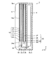
- the disassembled perspective view which shows the display apparatus of 1st Embodiment of this invention.
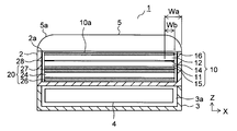
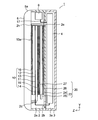
- Side surface sectional drawing which shows the display apparatus of 1st Embodiment of this invention.
- Front sectional view showing the display device of the first embodiment of the present invention.
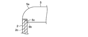
- Front sectional drawing which shows the detail of the junction part of the transparent member of the display apparatus of 1st Embodiment of this invention.
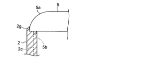
- Front sectional drawing which shows the detail of the other junction part of the transparent member of the display apparatus of 1st Embodiment of this invention.
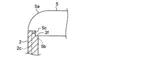
- Front sectional drawing which shows the detail of the other junction part of the transparent member of the display apparatus of 1st Embodiment of this invention.
- Front sectional drawing which shows the detail of the other junction part of the transparent member of the display apparatus of 1st Embodiment of this invention.
- Side surface sectional drawing which shows the display apparatus of 2nd Embodiment of this invention.
- Front sectional drawing which shows the display apparatus of 3rd Embodiment of this invention.
- Side surface sectional drawing which shows the display apparatus of 4th Embodiment of this invention.
- FIG. 1 is an exploded perspective view, a side sectional view, and a front sectional view showing the display device of the first embodiment.
- the display device 1 is held by an upper chassis 2 and a lower chassis 3 that form an outer peripheral surface of a mobile terminal device or the like.
- the upper chassis 2 and the lower chassis 3 are fixed by a double-sided adhesive tape (not shown) or the like.
- the lower chassis 3 is formed with a substrate storage portion 3a having an upper surface opened, and a circuit board 4, a battery (not shown), and the like are stored in the substrate storage portion 3a.
- the upper chassis 2 is formed with a recess 2a having an upper surface opened, and the display panel 10 and the backlight 20 having a rectangular shape in plan view are accommodated in the recess 2a.
- a transparent member 5 is disposed on the upper chassis 2.
- a display surface 10 a is formed on the upper surface of the display panel 10 facing the transparent member 5.
- the short side direction of the display panel 10 and the backlight 20 parallel to the display surface 10a is the X direction
- the direction orthogonal to the X direction in the plane parallel to the display surface 10a is the Y direction
- perpendicular to the display surface 10a is the Z direction.
- an insertion hole 2b that faces the substrate storage portion 3a.
- a plurality of fitting grooves 2c are formed on both side walls of the recess 2a facing each other in the X direction.
- the fitting groove 2c is disposed asymmetrically with respect to a center line orthogonal to the incident surface 24a of the light guide plate 24 described later.
- ribs 2d project from the upper portions of both side walls facing in the X direction.
- the inner wall of the recess 2a is subjected to a high reflection treatment by forming a reflection layer 28.
- the reflective layer 28 is formed on the upper chassis 2 by sputtering or plating a thin film such as aluminum or silver.
- the reflective layer 28 may be formed by printing with white ink.
- the upper chassis 2 may be made of metal and subjected to high reflection processing by mirror finishing. The light leaked from the light guide plate 24 and the optical sheet 27, which will be described later, is reflected by the reflective layer 28 (high reflection treatment), so that the light use efficiency can be improved and the luminance of the illumination light can be increased.
- the display panel 10 is formed of a liquid crystal panel or the like, and a pixel substrate 11 on which pixel electrodes are formed and a counter substrate 12 on which counter electrodes are formed are arranged to face each other.
- a liquid crystal 13 is sealed between the pixel substrate 11 and the counter substrate 12 by a sealing seal 14 disposed around the periphery.
- the frame width Wa of the display panel 10 is determined by the width Wb of the sealing seal 14 and the thickness of the upper chassis 2.
- the pixel substrate 11 and the counter substrate 12 are connected to the circuit substrate 4 through lead wires 18 made of FPC inserted through the insertion holes 2b on the bottom surface of the recess 2a.
- Optical sheets 15 and 16 made of a polarizing plate, a retardation film, and the like are bonded to the back surface of the pixel substrate 11 and the upper surface of the counter substrate 12, respectively.
- the backlight 20 is arranged on the back side of the display panel 10 and is configured as an edge light type in which a light source 25 is disposed opposite to a peripheral surface of a thin light guide plate 24.
- the light source 25 is composed of a plurality of LEDs, and opposes an incident surface 24a formed of a circumferential surface of the light guide plate 24 formed in a rectangular shape.
- the light incident from the incident surface 24a is guided through the light guide plate 24 and is emitted from the output surface 24d on the upper surface.
- the display panel 10 is illuminated from the back, and an image is displayed on the display surface 10a.
- An incident surface 24a may be formed on two opposite sides of the light guide plate 24, and the light source 25 may be disposed opposite to each incident surface 24a.
- the light guide plate 24 and the light source 25 form a light guide plate assembly 23 integrated by a holding member (not shown).
- the light source 25 is connected to the circuit board 4 via a lead wire (not shown).
- a reflective sheet 26 is disposed on the back surface of the light guide plate 24, and one or a plurality of optical sheets 27 formed of a diffusion sheet, a prism sheet, or the like are disposed on the top surface.
- the reflection sheet 26 and the optical sheet 27 are formed in substantially the same planar shape as the light guide plate 24.
- a protruding portion 29 that fits into the fitting groove 2c is provided.
- the reflective sheet 26 and the optical sheet 27 may be attached to the light guide plate 24 by a double-sided adhesive tape disposed on the protruding portion 29.
- the reflection sheet 26, the light guide plate assembly 23, and the optical sheet 27 constituting the backlight 20 are placed in order and accommodated in the recess 2a. At this time, the reflection sheet 26, the light guide plate assembly 23, and the optical sheet 27 are positioned in the X direction by the inner wall of the recess 2a, and are positioned in the Y direction by the fitting groove 2c. That is, the backlight 20 is fitted in the recess 2a and positioned in a plane parallel to the display surface 10a.
- the fitting groove 2c and the protruding portion 29 are asymmetrically arranged with respect to the center line orthogonal to the incident surface 24a of the light guide plate 24. For this reason, it is prevented that the direction of the back and front of the light guide plate assembly 23, the reflection sheet 26, and the optical sheet 27 is erroneously inserted. Therefore, the assembly of the display device 1 can be facilitated, the yield can be improved, and the cost can be reduced.
- the display panel 10 in which the optical sheet 15, the pixel substrate 11, the counter substrate 12, and the optical sheet 16 are integrated is similarly placed on the backlight 20 and accommodated in the recess 2a.
- the pixel substrate 11 of the display panel 10 is positioned in the X direction by the inner wall of the recess 2a, and is positioned in the Y direction by one inner wall of the recess 2a in the Y direction and the rib 2d. That is, the display panel 10 is positioned in a plane parallel to the display surface 10a by fitting into the recess 2a.
- the backlight 20 may be positioned in the Y direction by a rib protruding from the recess 2a.
- the display panel 10 may be positioned in the Y direction by providing protrusions that fit into the fitting grooves 2 c on the side surfaces of the pixel substrate 11 or the counter substrate 12 or the side surfaces of the optical sheets 15 and 16.
- the transparent member 5 is made of resin, glass or the like and is installed at the upper end of the upper chassis 2 to cover the recess 2a. As shown in FIG. 4, the joint between the transparent member 5 and the upper chassis 2 is provided with a protruding portion 5b that fits into the fitting groove 2c on the lower surface of the peripheral portion of the transparent member 5, and the transparent member 5 is positioned. Installed.
- the display panel 10 and the backlight 20 are positioned in a direction (Z direction) perpendicular to the display surface 10 a by the bottom surface of the recess 2 a and the transparent member 5.
- a step portion 5 c whose outer peripheral side is recessed may be formed on the peripheral portion of the lower surface of the transparent member 5.
- the transparent member 5 is installed so that the wall surface of the upper chassis 2 fits into the step portion 5c.
- a stepped portion 5 c that is recessed on the outer peripheral side may be formed on the peripheral portion of the lower surface of the transparent member 5, and a stepped portion 2 f that is recessed on the inner peripheral side may be formed on the wall surface of the upper chassis 2.
- the wall surface of the upper chassis 2 is fitted into the step portion 5c, and the transparent member 5 is installed on the bottom surface of the step portion 2f.
- a stepped portion 2 g whose inner peripheral side is recessed may be formed on the wall surface of the upper chassis 2.
- the transparent member 5 is fitted on the peripheral surface of the step portion 2g and installed on the bottom surface of the step portion 2g.
- a curved surface portion 5 a is formed on the periphery of the upper surface of the transparent member 5.
- the light is refracted by the curved surface portion 5a of the transparent member 5, and is visually recognized as a narrower frame than the actual frame width Wa.
- the thickness t of the transparent member 5 and the radius of curvature r of the curved surface portion 5a have the relationship shown in the expressions (1) and (2), where Wa is the frame width of the display device 1.
- the gaps in the X direction and the Y direction between the display panel 10 and the backlight 20 and the recess 2a are, for example, about several tens of ⁇ m. Further, when the display surface 10a is disposed facing upward, the gap in the Z direction between the lower surface of the transparent member 5 and the display panel 10 is, for example, about several tens of micrometers, and the lower surface of the transparent member 5 is the display panel. 10 close.
- the display panel 10 and the backlight 20 are arranged so as to be movable within the gap in the recess 2a. At this time, the display area of the display device 1 can be prevented from deteriorating by forming the illumination light emission area of the backlight 20 larger than the display area of the display panel 10 by a predetermined amount.
- the display panel 10 and the backlight 20 may be fixed in the recess 2a with an adhesive injected into the recess 2a.
- the transparent member 5 and the display panel 10 may be in contact with each other and the display panel 10 and the backlight 20 may be sandwiched between the transparent member 5 and the bottom surface of the recess 2a. Thereby, sliding of the display panel 10 and the backlight 20 can be prevented.
- the display panel 10 and the backlight 20 are fitted in the recess 2a of the upper chassis 2 and positioned in the X and Y directions in a plane parallel to the display surface 10a, and the bottom surface of the recess 2a and the transparent member 5 are positioned. Is positioned in the direction (Z direction) perpendicular to the display surface 10a.
- the double-sided adhesive tape which joins the display panel 10 and the backlight 20 like a prior art example can be omitted. Therefore, it is possible to reduce the number of manufacturing steps of the display device 1 and to secure a display quality and to narrow the frame.
- the display device 1 can be easily formed by sequentially placing the light guide plate assembly 23 and the like constituting the backlight 20 and the display panel 10.
- the substrate storage portion 3a for storing the circuit board 4 is provided on the back side of the recess 2a and the insertion hole 2b of the lead wire 18 is provided on the bottom surface of the recess 2a, the lead wire 18 can be shortened and easily displayed. And the circuit board 4 can be connected.
- FIG. 8 shows a side sectional view of the display device 1 of the second embodiment.
- an imaging device 6 such as a CCD for photographing a subject is arranged in the upper chassis 2.
- Other parts are the same as those in the first embodiment.
- an insertion hole 2e is provided at the end opposite to the insertion hole 2b.
- ribs 2h are projected from both side walls facing in the X direction.
- the image pickup device 6 is arranged on the outer peripheral side of the rib 2h, and is connected to the circuit board 4 via a lead wire 17 made of FPC inserted through the insertion hole 2e.
- the backlight 20 and the display panel 10 are arranged on the inner peripheral side with respect to the rib 2h, and the pixel substrate 11 of the display panel 10 is fitted between the rib 2h and the rib 2d and positioned in the Y direction. Thereby, the effect similar to 1st Embodiment can be acquired.
- FIG. 9 shows a side sectional view of the display device 1 of the third embodiment.
- a step 2 m is provided in the recess 2 a of the upper chassis 2.
- Other parts are the same as those in the first embodiment.
- the upper chassis 2 is formed such that the thickness of the lower portion of the concave portion 2a is thicker than the upper portion, and a stepped portion 2m having a narrow lower portion is formed in the concave portion 2a. Further, a plurality of fitting grooves 2c (see FIG. 1) are formed on both side walls of the recess 2a facing each other in the X direction over the upper and lower steps of the step 2m.
- the backlight 20 is disposed on the lower stage of the stepped portion 2m, and the display panel 10 is placed on the horizontal plane of the stepped portion 2m and disposed on the upper stage.
- the reflection sheet 26, the light guide plate assembly 23, and the optical sheet 27 constituting the backlight 20 are positioned in the X direction by the lower inner wall of the step portion 2m, and are positioned in the Y direction by the fitting groove 2c. That is, the backlight 20 is fitted in the recess 2a and positioned in a plane parallel to the display surface 10a.
- the pixel substrate 11 of the display panel 10 is positioned in the X direction by the upper inner wall of the stepped portion 2m, and is positioned in the Y direction by one inner wall in the Y direction of the recess 2a and the rib 2d. That is, the display panel 10 is positioned in a plane parallel to the display surface 10a by fitting into the recess 2a.
- the display panel 10 and the backlight 20 are positioned in a direction (Z direction) perpendicular to the display surface 10a by the bottom surface of the recess 2a and the transparent member 5.
- the optical sheet 16 on the upper surface of the display panel 10 and the transparent member 5 may be in contact with each other or may be close to each other.
- the optical sheet 15 on the lower surface of the display panel 10 may be in contact with or close to the optical sheet 27 on the upper surface of the backlight 20.
- the same effect as that of the first embodiment can be obtained.
- the backlight 20 is fitted to the lower stage of the step part 2m formed in the recess 2a, and the display panel 10 is fitted to the upper stage. For this reason, it is possible to prevent the display panel 10 from being erroneously inserted into the lower stage narrower than the upper stage of the stepped portion 2m, and to facilitate the assembly of the display device 1.
- FIG. 10 shows a side sectional view of the display device 1 of the fourth embodiment.
- the same reference numerals are given to the same parts as those of the first embodiment shown in FIGS.
- the bottom surface of the recess 2 a of the upper chassis 2 is opened and is closed by the reflection sheet 26.
- Other parts are the same as those in the first embodiment.
- the recess 2a formed in the upper chassis 2 is formed with an opening 2k surrounded by a mounting portion 2j protruding from the inner peripheral wall with the bottom open.
- the reflection sheet 26 arranged in the lower layer of the backlight 20 is bridged between the mounting parts 2j facing each other, and the bottom of the recess 2a is closed by the reflection sheet 26.
- the reflection sheet 26 is provided with an insertion hole 26a through which the lead wire 18 is inserted.
- the same effect as that of the first embodiment can be obtained. Further, since the upper chassis 2 has the opening 2k by opening the bottom surface of the recess 2a, the weight of the display device 1 can be reduced. Further, since the circuit board 4 and the like can be installed in the board housing part 3a through the opening 2k, the number of parts of the display device 1 can be reduced by integrally molding the upper chassis 2 and the lower chassis 3. .
- a step 2m (see FIG. 9) may be provided in the recess 2a.
- a device such as a mobile terminal device (a mobile phone, a tablet terminal, etc.) using an edge light type backlight.
Landscapes
- Physics & Mathematics (AREA)
- Nonlinear Science (AREA)
- Mathematical Physics (AREA)
- Chemical & Material Sciences (AREA)
- Crystallography & Structural Chemistry (AREA)
- General Physics & Mathematics (AREA)
- Optics & Photonics (AREA)
- Liquid Crystal (AREA)
Abstract
表示パネル10と、表示パネル10を背面から照明するバックライト20と、前面を開口した凹部2aが形成されるシャーシ2と、凹部2aを覆う透明部材5とを備え、表示パネル10及びバックライト20を凹部2a内に収納する表示装置1において、表示パネル10及びバックライト20が凹部2aに嵌合して表示パネル10の表示面10aに平行な面内で位置決めされるとともに、凹部2aの底面及び透明部材5によって表示面10aに垂直方向に位置決めされるようにした。
Description
本発明は、バックライト及び表示パネルを備えた表示装置に関する。
従来の表示装置は特許文献1に開示されている。この表示装置は表示パネルの背面にバックライトが配される。バックライトは上面を開口する金属ケース内に収納され、バックライトの上面周部に配した両面粘着テープによって表示パネルがバックライト上に固定される。バックライトから出射された照明光により表示パネルが背面から照明され、表示パネルの表示領域に画像が表示される。
表示パネルの表示領域の周囲には遮光された額縁領域が形成される。表示パネルとバックライトとを固着する両面粘着テープは表示パネルの額縁領域により覆われ、表示領域の正面から見て両面粘着テープの内周縁が識別できない状態になっている。
この時、表示パネルの表示面の法線に対して斜め方向から表示領域を見た際に、照明光を遮る両面粘着テープの内縁が識別されると表示装置の表示品位が低下する。このため、表示面の法線に対して所定の角度範囲で表示装置の表示品位を確保するために、表示パネルの額縁領域の幅と両面粘着テープの幅との差が所定量設けられる。例えば、表示面の法線に対して30゜の範囲で表示品位を確保するために、両面粘着テープの幅に対して表示パネルの額縁幅が約0.4mm大きく形成される。
表示装置は携帯端末装置等に用いられ、薄型化や表示領域の周囲のスペースを狭くする狭額縁化のニーズが高い。しかしながら、上記従来の表示装置によると、表示パネルの額縁幅が小さくなると更に幅の小さい両面粘着テープを容易に形成できないため製造工数が大きくなる問題があった。
また、両面粘着テープの幅の加工限界が0.5mm程度であるため、表示品位を確保するために表示パネルの額縁幅が約0.9mmになり、表示装置の狭額縁化を図ることが困難になる問題もあった。
本発明は、製造工数を削減できるとともに表示品位を低下させずに狭額縁化を図ることのできる表示装置を提供することを目的とする。
上記目的を達成するために本発明は表示パネルと、前記表示パネルを背面から照明するバックライトと、前面を開口した凹部が形成されるシャーシと、前記凹部を覆う透明部材とを備え、前記表示パネル及び前記バックライトを前記凹部内に収納する表示装置において、前記表示パネル及び前記バックライトが前記凹部に嵌合して前記表示パネルの表示面に平行な面内で位置決めされるとともに、前記凹部の底面及び前記透明部材によって前記表示面に垂直方向に位置決めされることを特徴としている。
この構成によると、バックライト及び表示パネルはシャーシに設けた凹部に嵌合し、表示面に平行な面内で位置決めして収納される。また、バックライト及び表示パネルは凹部の底面とシャーシ上に配した透明部材との間に挟まれ、表示面に垂直方向に位置決めされる。
また本発明は、上記構成の表示装置において、前記表示面を上方に面して配置した際に、前記凹部の底面に前記バックライトが接するとともに前記バックライト上に前記表示パネルが接し、前記透明部材の下面が前記表示パネルに近接または接触することを特徴としている。
また本発明は、上記構成の表示装置において、前記凹部は背面側が狭い段差部を有し、前記段差部の下段に前記バックライトが嵌合して上段に前記表示パネルが嵌合することを特徴としている。
また本発明は、上記構成の表示装置において、前記凹部の底面が開放されるとともに前記凹部の内周壁から突出する載置部を設け、前記バックライトに設けた反射シートを対向する前記載置部間に橋架したことを特徴としている。
また本発明は、上記構成の表示装置において、前記凹部の背面側に前記表示パネルの回路基板を収納する基板収納部を有し、前記表示パネルと前記回路基板とを接続するリード線の挿通孔を前記凹部の底面に設けたことを特徴としている。
本発明によると、表示パネル及びバックライトがシャーシの凹部に嵌合して表示面に平行な面内で位置決めされ、凹部の底面及び透明部材によって表示面に垂直方向に位置決めされる。これにより、従来例のように表示パネルとバックライトとを接合する両面粘着テープを省くことができる。従って、表示装置の製造工数を削減できるとともに表示品位を確保して狭額縁化を図ることができる。
<第1実施形態>
以下に図面を参照して本発明の実施形態を説明する。図1、図2、図3は第1実施形態の表示装置を示す分解斜視図、側面断面図及び正面断面図である。表示装置1は携帯端末装置等の外周面を形成する上シャーシ2及び下シャーシ3に保持される。上シャーシ2と下シャーシ3とは両面粘着テープ(不図示)等により固着される。
以下に図面を参照して本発明の実施形態を説明する。図1、図2、図3は第1実施形態の表示装置を示す分解斜視図、側面断面図及び正面断面図である。表示装置1は携帯端末装置等の外周面を形成する上シャーシ2及び下シャーシ3に保持される。上シャーシ2と下シャーシ3とは両面粘着テープ(不図示)等により固着される。
下シャーシ3には上面を開口する基板収納部3aが形成され、回路基板4やバッテリ(不図示)等が基板収納部3a内に収納される。上シャーシ2には上面を開口する凹部2aが形成され、平面視矩形の表示パネル10及びバックライト20が凹部2a内に収納される。また、上シャーシ2上には透明部材5が配される。透明部材5に対向する表示パネル10の上面に表示面10aが形成される。
以下の説明において、表示面10aに平行な表示パネル10及びバックライト20の短手方向をX方向、表示面10aに平行な面内でX方向に直交する方向をY方向、表示面10aに垂直な方向をZ方向とする。
上シャーシ2の凹部2aの底面の一端部には基板収納部3aに臨む挿通孔2bが設けられる。凹部2aのX方向に対向する両側壁には複数の嵌合溝2cが形成される。嵌合溝2cは後述する導光板24の入射面24aに直交する中心線に対して非対称に配置される。凹部2aの挿通孔2b近傍にはX方向に対向する両側壁の上部にリブ2dが突設される。
また、凹部2aの内壁には反射層28の形成により高反射処理が施される。反射層28は上シャーシ2上にアルミニウムや銀等の薄膜のスパッタリングやメッキにより形成される。反射層28を白色インクの印刷により形成してもよい。また、上シャーシ2を金属により形成して鏡面加工により高反射処理を施してもよい。反射層28(高反射処理)によって後述する導光板24や光学シート27から漏れた光を反射し、光利用効率が向上して照明光の輝度を高くすることができる。
表示パネル10は液晶パネル等により形成され、画素電極を形成した画素基板11と対向電極を形成した対向基板12とが対向配置される。画素基板11と対向基板12との間には周部に配した封止シール14により液晶13が封入される。封止シール14の幅Wb及び上シャーシ2の肉厚によって表示パネル10の額縁幅Waが決められる。
画素基板11及び対向基板12は凹部2aの底面の挿通孔2bに挿通したFPCから成るリード線18を介して回路基板4に接続される。画素基板11の背面及び対向基板12の上面にはそれぞれ偏光板や位相差フィルム等から成る光学シート15、16が接着される。
バックライト20は表示パネル10の背面側に配され、薄板状の導光板24の周面に光源25を対向配置したエッジライト型に構成される。光源25は複数のLEDから成り、矩形に形成される導光板24の短手方向の一周面から成る入射面24aに対向する。入射面24aから入射した光は導光板24を導光し、上面の出射面24dから出射される。これにより、表示パネル10が背面から照明され、表示面10aに画像が表示される。導光板24の対向する二辺に入射面24aを形成して光源25を各入射面24aに対向配置してもよい。
導光板24及び光源25は保持部材(不図示)により一体化された導光板組品23を形成する。光源25はリード線(不図示)を介して回路基板4に接続される。また、導光板24の背面には反射シート26が配され、上面には拡散シートやプリズムシート等により形成される一または複数の光学シート27が配される。
反射シート26及び光学シート27は導光板24と略同一の平面形状に形成される。導光板24、反射シート26及び光学シート27の周面には嵌合溝2cに嵌合する突出部29が突設される。反射シート26及び光学シート27を突出部29上に配した両面粘着テープによって導光板24に貼着してもよい。
バックライト20を構成する反射シート26、導光板組品23及び光学シート27は順に載置して凹部2a内に収納される。この時、反射シート26、導光板組品23及び光学シート27は凹部2aの内壁によってX方向に位置決めされ、嵌合溝2cによってY方向に位置決めされる。即ち、バックライト20は凹部2aに嵌合して表示面10aに平行な面内で位置決めされる。
この時、導光板24の入射面24aに直交する中心線に対して嵌合溝2c及び突出部29が非対称に配置される。このため、導光板組品23、反射シート26、光学シート27の裏表等の向きを誤って挿入することが防止される。従って、表示装置1の組み立てを容易にし、歩留まりを向上するとともにコストを削減することができる。
また、光学シート15、画素基板11、対向基板12及び光学シート16を一体化した表示パネル10も同様にバックライト20上に載置して凹部2a内に収納される。この時、表示パネル10の画素基板11は凹部2aの内壁によってX方向に位置決めされ、凹部2aのY方向の一方の内壁とリブ2dとによってY方向に位置決めされる。即ち、表示パネル10は凹部2aに嵌合して表示面10aに平行な面内で位置決めされる。
バックライト20を凹部2aに突設したリブによりY方向に位置決めしてもよい。また、嵌合溝2cに嵌合する突出部を画素基板11または対向基板12の側面や光学シート15、16の側面に設けて表示パネル10をY方向に位置決めしてもよい。
透明部材5は樹脂やガラス等により形成され、上シャーシ2の上端に設置して凹部2aを覆う。透明部材5と上シャーシ2との接合部は図4に示すように、透明部材5の周部の下面に嵌合溝2cに嵌合する突出部5bが設けられ、透明部材5が位置決めして設置される。表示パネル10及びバックライト20は凹部2aの底面及び透明部材5によって表示面10aに垂直な方向(Z方向)に位置決めされる。
図5に示すように、透明部材5の下面の周部に外周側が凹む段差部5cを形成してもよい。この時、上シャーシ2の壁面が段差部5cに嵌合するように透明部材5が設置される。また、図6に示すように、透明部材5の下面の周部に外周側が凹む段差部5cを形成し、上シャーシ2の壁面に内周側が凹む段差部2fを形成してもよい。この時、上シャーシ2の壁面が段差部5cに嵌合するとともに、透明部材5が段差部2fの底面上に設置される。また、図7に示すように、上シャーシ2の壁面に内周側が凹む段差部2gを形成してもよい。この時、透明部材5が段差部2gの周面に嵌合して段差部2gの底面上に設置される。
透明部材5の上面の周部には曲面の曲面部5aが形成される。これにより、表示装置1を正面から見た際に透明部材5の曲面部5aで光が屈折し、実際の額縁幅Waよりも狭額縁に視認される。透明部材5の厚みt及び曲面部5aの曲率半径rは表示装置1の額縁幅をWaとして式(1)、式(2)に示す関係を有すると望ましい。
t=2.7Wa~4.6Wa ・・・(1)
r=1.6Wa~4.2Wa ・・・(2)
r=1.6Wa~4.2Wa ・・・(2)
表示パネル10及びバックライト20と凹部2aとのX方向及びY方向の隙間は例えば、数十μm程度に形成される。また、表示面10aを上方に面して配置した際に、透明部材5の下面と表示パネル10とのZ方向の隙間は例えば、数十μm程度に形成され、透明部材5の下面が表示パネル10に近接する。
これにより、表示パネル10及びバックライト20が凹部2a内で該隙間の範囲で移動可能に配される。この時、表示パネル10の表示領域よりもバックライト20の照明光の出射領域を所定量だけ大きく形成することにより、表示装置1の表示品位の低下を防止することができる。
尚、凹部2a内に注入した接着剤により表示パネル10及びバックライト20を凹部2a内に固着してもよい。また、透明部材5と表示パネル10とが接して透明部材5及び凹部2aの底面によって表示パネル10及びバックライト20を挟持してもよい。これにより、表示パネル10及びバックライト20の摺動を防止することができる。
本実施形態によると、表示パネル10及びバックライト20が上シャーシ2の凹部2aに嵌合して表示面10aに平行な面内でX、Y方向に位置決めされ、凹部2aの底面及び透明部材5によって表示面10aに垂直な方向(Z方向)に位置決めされる。これにより、従来例のように表示パネル10とバックライト20とを接合する両面粘着テープを省くことができる。従って、表示装置1の製造工数を削減できるとともに表示品位を確保して狭額縁化を図ることができる。
また、表示面10aを上方に面して配置した際に、凹部2aの底面にバックライト20が接してバックライト20上に表示パネル10が接し、透明部材5の下面が表示パネル10に近接または接触する。これにより、バックライト20を構成する導光板組品23等や表示パネル10を順に載置して容易に表示装置1を形成することができる。
また、回路基板4を収納する基板収納部3aを凹部2aの背面側に設け、リード線18の挿通孔2bを凹部2aの底面に設けたので、リード線18を短縮して容易に表示パネル10と回路基板4とを接続することができる。
<第2実施形態>
次に、図8は第2実施形態の表示装置1の側面断面図を示している。説明の便宜上、前述の図1~図7に示す第1実施形態と同様の部分には同一の符号を付している。本実施形態は上シャーシ2内に被写体の撮影を行うCCD等の撮像素子6が配される。その他の部分は第1実施形態と同様である。
次に、図8は第2実施形態の表示装置1の側面断面図を示している。説明の便宜上、前述の図1~図7に示す第1実施形態と同様の部分には同一の符号を付している。本実施形態は上シャーシ2内に被写体の撮影を行うCCD等の撮像素子6が配される。その他の部分は第1実施形態と同様である。
上シャーシ2の凹部2aの底面には挿通孔2bの反対側の端部に挿通孔2eが設けられる。凹部2aの挿通孔2e近傍にはX方向に対向する両側壁にリブ2hが突設される。撮像素子6はリブ2hの外周側に配され、挿通孔2eに挿通されるFPCから成るリード線17を介して回路基板4に接続される。また、バックライト20及び表示パネル10はリブ2hよりも内周側に配され、表示パネル10の画素基板11はリブ2hとリブ2dとの間に嵌合してY方向に位置決めされる。これにより、第1実施形態と同様の効果を得ることができる。
<第3実施形態>
次に、図9は第3実施形態の表示装置1の側面断面図を示している。説明の便宜上、前述の図1~図7に示す第1実施形態と同様の部分には同一の符号を付している。本実施形態は上シャーシ2の凹部2a内に段差部2mが設けられる。その他の部分は第1実施形態と同様である。
次に、図9は第3実施形態の表示装置1の側面断面図を示している。説明の便宜上、前述の図1~図7に示す第1実施形態と同様の部分には同一の符号を付している。本実施形態は上シャーシ2の凹部2a内に段差部2mが設けられる。その他の部分は第1実施形態と同様である。
上シャーシ2は凹部2aの下部の肉厚が上部よりも厚く形成され、凹部2a内に下方が狭い段差部2mが形成される。また、凹部2aのX方向に対向する両側壁には段差部2mの上下段にわたって複数の嵌合溝2c(図1参照)が形成される。バックライト20は段差部2mの下段に配され、表示パネル10は段差部2mの水平面上に載置して上段に配される。
この時、バックライト20を構成する反射シート26、導光板組品23及び光学シート27は段差部2mの下段の内壁によってX方向に位置決めされ、嵌合溝2cによってY方向に位置決めされる。即ち、バックライト20は凹部2aに嵌合して表示面10aに平行な面内で位置決めされる。
また、表示パネル10の画素基板11は段差部2mの上段の内壁によってX方向に位置決めされ、凹部2aのY方向の一方の内壁とリブ2dとによってY方向に位置決めされる。即ち、表示パネル10は凹部2aに嵌合して表示面10aに平行な面内で位置決めされる。
また、表示パネル10及びバックライト20は凹部2aの底面及び透明部材5によって表示面10aに垂直な方向(Z方向)に位置決めされる。この時、表示パネル10の上面の光学シート16と透明部材5とが接してもよく、近接してもよい。また、表示パネル10の下面の光学シート15とバックライト20の上面の光学シート27とが接してもよく、近接してもよい。
本実施形態によると、第1実施形態と同様の効果を得ることができる。また、凹部2a内に形成した段差部2mの下段にバックライト20が嵌合して上段に表示パネル10が嵌合する。このため、段差部2mの上段よりも狭い下段に表示パネル10が誤挿入されることを防止し、表示装置1の組み立てを容易にすることができる。
<第4実施形態>
次に、図10は第4実施形態の表示装置1の側面断面図を示している。説明の便宜上、前述の図1~図7に示す第1実施形態と同様の部分には同一の符号を付している。本実施形態は上シャーシ2の凹部2aの底面が開放され、反射シート26により塞がれる。その他の部分は第1実施形態と同様である。
次に、図10は第4実施形態の表示装置1の側面断面図を示している。説明の便宜上、前述の図1~図7に示す第1実施形態と同様の部分には同一の符号を付している。本実施形態は上シャーシ2の凹部2aの底面が開放され、反射シート26により塞がれる。その他の部分は第1実施形態と同様である。
上シャーシ2に形成される凹部2aは底面を開放して内周壁から突出する載置部2jにより周囲を囲まれた開口部2kが形成される。バックライト20の下層に配される反射シート26は対向する載置部2j間に橋架され、凹部2aの底部が反射シート26により塞がれる。また、反射シート26にはリード線18が挿通される挿通孔26aが設けられる。
本実施形態によると、第1実施形態と同様の効果を得ることができる。また、上シャーシ2が凹部2aの底面を開放して開口部2kを有するため、表示装置1の軽量化を図ることができる。また、開口部2kを介して回路基板4等を基板収納部3aに設置できるため、上シャーシ2と下シャーシ3とを一体に成形することにより、表示装置1の部品点数を削減することができる。
本実施形態において、第3実施形態と同様に凹部2a内に段差部2m(図9参照)を設けてもよい。
本発明によると、エッジライト型のバックライトを用いた携帯端末装置(携帯電話機やタブレット端末等)等の機器に利用することができる。
1 表示装置
2 上シャーシ
2a 凹部
2c 嵌合溝
2j 載置部
2m 段差部
3 下シャーシ
3a 基板収納部
4 回路基板
5 透明部材
5a 曲面部
6 撮像素子
10 表示パネル
10a 表示面
11 画素基板
12 対向基板
13 液晶
14 封止シール
15、16 光学シート
17、18 リード線
20 バックライト
23 導光板組品
24 導光板
24a 入射面
24d 出射面
25 光源
26 反射シート
27 光学シート
29 突出部
2 上シャーシ
2a 凹部
2c 嵌合溝
2j 載置部
2m 段差部
3 下シャーシ
3a 基板収納部
4 回路基板
5 透明部材
5a 曲面部
6 撮像素子
10 表示パネル
10a 表示面
11 画素基板
12 対向基板
13 液晶
14 封止シール
15、16 光学シート
17、18 リード線
20 バックライト
23 導光板組品
24 導光板
24a 入射面
24d 出射面
25 光源
26 反射シート
27 光学シート
29 突出部
Claims (5)
- 表示パネルと、前記表示パネルを背面から照明するバックライトと、前面を開口した凹部が形成されるシャーシと、前記凹部を覆う透明部材とを備え、前記表示パネル及び前記バックライトを前記凹部内に収納する表示装置において、前記表示パネル及び前記バックライトが前記凹部に嵌合して前記表示パネルの表示面に平行な面内で位置決めされるとともに、前記凹部の底面及び前記透明部材によって前記表示面に垂直方向に位置決めされることを特徴とする表示装置。
- 前記表示面を上方に面して配置した際に、前記凹部の底面に前記バックライトが接するとともに前記バックライト上に前記表示パネルが接し、前記透明部材の下面が前記表示パネルに近接または接触することを特徴とする請求項1に記載の表示装置。
- 前記凹部は背面側が狭い段差部を有し、前記段差部の下段に前記バックライトが嵌合して上段に前記表示パネルが嵌合することを特徴とする請求項1に記載の表示装置。
- 前記凹部の底面が開放されるとともに前記凹部の内周壁から突出する載置部を設け、前記バックライトに設けた反射シートを対向する前記載置部間に橋架したことを特徴とする請求項1~請求項3のいずれかに記載の表示装置。
- 前記凹部の背面側に前記表示パネルの回路基板を収納する基板収納部を有し、前記表示パネルと前記回路基板とを接続するリード線の挿通孔を前記凹部の底面に設けたことを特徴とする請求項1~請求項3のいずれかに記載の表示装置。
Priority Applications (1)
| Application Number | Priority Date | Filing Date | Title |
|---|---|---|---|
| US14/435,223 US20150286086A1 (en) | 2012-10-26 | 2013-09-25 | Display device |
Applications Claiming Priority (2)
| Application Number | Priority Date | Filing Date | Title |
|---|---|---|---|
| JP2012-236346 | 2012-10-26 | ||
| JP2012236346 | 2012-10-26 |
Publications (1)
| Publication Number | Publication Date |
|---|---|
| WO2014065064A1 true WO2014065064A1 (ja) | 2014-05-01 |
Family
ID=50544444
Family Applications (1)
| Application Number | Title | Priority Date | Filing Date |
|---|---|---|---|
| PCT/JP2013/075834 Ceased WO2014065064A1 (ja) | 2012-10-26 | 2013-09-25 | 表示装置 |
Country Status (2)
| Country | Link |
|---|---|
| US (1) | US20150286086A1 (ja) |
| WO (1) | WO2014065064A1 (ja) |
Cited By (9)
| Publication number | Priority date | Publication date | Assignee | Title |
|---|---|---|---|---|
| CN104460084A (zh) * | 2014-12-10 | 2015-03-25 | 深圳市华星光电技术有限公司 | 一种用于液晶显示的边框结构 |
| CN104698684A (zh) * | 2014-08-22 | 2015-06-10 | 努比亚技术有限公司 | 显示面板组件和显示装置 |
| WO2016026467A1 (zh) * | 2014-08-22 | 2016-02-25 | 努比亚技术有限公司 | 一种无边框显示装置及移动终端 |
| WO2016192445A1 (zh) * | 2015-05-29 | 2016-12-08 | 广东欧珀移动通信有限公司 | 显示屏面板及具有显示屏面板的移动终端 |
| JP2017002293A (ja) * | 2015-06-15 | 2017-01-05 | 日東電工株式会社 | 固定部材 |
| JP2017103168A (ja) * | 2015-12-04 | 2017-06-08 | 三菱電機株式会社 | バックライトおよび表示装置 |
| TWI637215B (zh) * | 2015-08-10 | 2018-10-01 | 揚昇照明股份有限公司 | 顯示裝置 |
| JP2022158032A (ja) * | 2021-04-01 | 2022-10-14 | 株式会社デンソー | 表示装置 |
| WO2022267734A1 (zh) * | 2021-06-22 | 2022-12-29 | 华为技术有限公司 | 显示模组及显示设备 |
Families Citing this family (1)
| Publication number | Priority date | Publication date | Assignee | Title |
|---|---|---|---|---|
| KR102504803B1 (ko) * | 2016-04-06 | 2023-02-28 | 엘지전자 주식회사 | 디스플레이 디바이스 |
Citations (4)
| Publication number | Priority date | Publication date | Assignee | Title |
|---|---|---|---|---|
| JP2009020430A (ja) * | 2007-07-13 | 2009-01-29 | Nippon Seiki Co Ltd | 表示装置 |
| JP2009192769A (ja) * | 2008-02-14 | 2009-08-27 | Hitachi Displays Ltd | 液晶表示装置 |
| JP2011209470A (ja) * | 2010-03-29 | 2011-10-20 | Seiko Instruments Inc | 液晶表示装置及びその製造方法、電子機器 |
| JP2012043860A (ja) * | 2010-08-16 | 2012-03-01 | Panasonic Corp | 発光装置、バックライトユニット、液晶表示装置及び照明装置 |
Family Cites Families (3)
| Publication number | Priority date | Publication date | Assignee | Title |
|---|---|---|---|---|
| JP2008197125A (ja) * | 2005-05-24 | 2008-08-28 | Sharp Corp | 液晶表示装置 |
| KR101706101B1 (ko) * | 2010-04-20 | 2017-02-14 | 삼성전자주식회사 | 디스플레이 장치 |
| KR101966070B1 (ko) * | 2012-02-21 | 2019-04-08 | 삼성디스플레이 주식회사 | 표시장치 및 이의 제조방법 |
-
2013
- 2013-09-25 WO PCT/JP2013/075834 patent/WO2014065064A1/ja not_active Ceased
- 2013-09-25 US US14/435,223 patent/US20150286086A1/en not_active Abandoned
Patent Citations (4)
| Publication number | Priority date | Publication date | Assignee | Title |
|---|---|---|---|---|
| JP2009020430A (ja) * | 2007-07-13 | 2009-01-29 | Nippon Seiki Co Ltd | 表示装置 |
| JP2009192769A (ja) * | 2008-02-14 | 2009-08-27 | Hitachi Displays Ltd | 液晶表示装置 |
| JP2011209470A (ja) * | 2010-03-29 | 2011-10-20 | Seiko Instruments Inc | 液晶表示装置及びその製造方法、電子機器 |
| JP2012043860A (ja) * | 2010-08-16 | 2012-03-01 | Panasonic Corp | 発光装置、バックライトユニット、液晶表示装置及び照明装置 |
Cited By (15)
| Publication number | Priority date | Publication date | Assignee | Title |
|---|---|---|---|---|
| CN105093624B (zh) * | 2014-08-22 | 2017-09-08 | 努比亚技术有限公司 | 无边框终端及其制造方法 |
| CN105093624A (zh) * | 2014-08-22 | 2015-11-25 | 努比亚技术有限公司 | 无边框终端及其制造方法 |
| WO2016026385A1 (zh) * | 2014-08-22 | 2016-02-25 | 努比亚技术有限公司 | 一种无边框显示装置 |
| WO2016026467A1 (zh) * | 2014-08-22 | 2016-02-25 | 努比亚技术有限公司 | 一种无边框显示装置及移动终端 |
| CN104698684A (zh) * | 2014-08-22 | 2015-06-10 | 努比亚技术有限公司 | 显示面板组件和显示装置 |
| EP3185066A4 (en) * | 2014-08-22 | 2017-06-28 | Nubia Technology Co., Ltd. | Frameless display device and mobile terminal |
| CN104460084A (zh) * | 2014-12-10 | 2015-03-25 | 深圳市华星光电技术有限公司 | 一种用于液晶显示的边框结构 |
| WO2016192445A1 (zh) * | 2015-05-29 | 2016-12-08 | 广东欧珀移动通信有限公司 | 显示屏面板及具有显示屏面板的移动终端 |
| JP2017002293A (ja) * | 2015-06-15 | 2017-01-05 | 日東電工株式会社 | 固定部材 |
| TWI637215B (zh) * | 2015-08-10 | 2018-10-01 | 揚昇照明股份有限公司 | 顯示裝置 |
| US10126487B2 (en) | 2015-08-10 | 2018-11-13 | Young Lighting Technology Inc. | Display device |
| JP2017103168A (ja) * | 2015-12-04 | 2017-06-08 | 三菱電機株式会社 | バックライトおよび表示装置 |
| JP2022158032A (ja) * | 2021-04-01 | 2022-10-14 | 株式会社デンソー | 表示装置 |
| JP7435526B2 (ja) | 2021-04-01 | 2024-02-21 | 株式会社デンソー | 表示装置 |
| WO2022267734A1 (zh) * | 2021-06-22 | 2022-12-29 | 华为技术有限公司 | 显示模组及显示设备 |
Also Published As
| Publication number | Publication date |
|---|---|
| US20150286086A1 (en) | 2015-10-08 |
Similar Documents
| Publication | Publication Date | Title |
|---|---|---|
| WO2014065064A1 (ja) | 表示装置 | |
| KR101348247B1 (ko) | 액정 표시 장치 | |
| JP5436935B2 (ja) | 液晶表示装置 | |
| JP2003255309A (ja) | 光学ユニット及びそれを用いた液晶表示装置 | |
| JP4970177B2 (ja) | 面発光装置及び表示装置 | |
| US10969625B2 (en) | Liquid crystal display device having high screen ratio | |
| US9423555B2 (en) | Backlight and display apparatus | |
| JP2016085416A (ja) | 液晶表示装置 | |
| JP4730434B2 (ja) | スクリーン組立体及び背面投射型映像表示装置 | |
| WO2018051855A1 (ja) | 光学部材、照明装置及び表示装置 | |
| CN110474997A (zh) | 终端设备 | |
| KR20110088811A (ko) | 백라이트 어셈블리 및 그를 포함하는 표시 장치 | |
| US11016321B2 (en) | Display device having frame member with folded-back portion bonded to sealing member | |
| WO2018177279A1 (zh) | 背光结构和显示装置 | |
| CN105546403B (zh) | 面状照明装置、液晶显示装置以及其组装方法 | |
| KR101929378B1 (ko) | 액정표시장치 | |
| JP2016081785A (ja) | 面光源装置、表示装置、及び電子機器 | |
| US10969621B2 (en) | Display assembly and display device | |
| JP4449039B2 (ja) | 面状照明装置およびその組立方法 | |
| JP5650005B2 (ja) | 液晶表示装置 | |
| JP6693139B2 (ja) | 筐体、面光源装置、表示装置、及び電子機器 | |
| JP2015068972A (ja) | 液晶表示装置 | |
| JP2013068869A (ja) | 液晶表示装置 | |
| KR101820282B1 (ko) | 디스플레이 장치 | |
| CN210166601U (zh) | 导光板、背光模组、显示装置 |
Legal Events
| Date | Code | Title | Description |
|---|---|---|---|
| 121 | Ep: the epo has been informed by wipo that ep was designated in this application |
Ref document number: 13848870 Country of ref document: EP Kind code of ref document: A1 |
|
| WWE | Wipo information: entry into national phase |
Ref document number: 14435223 Country of ref document: US |
|
| NENP | Non-entry into the national phase |
Ref country code: DE |
|
| 122 | Ep: pct application non-entry in european phase |
Ref document number: 13848870 Country of ref document: EP Kind code of ref document: A1 |
|
| NENP | Non-entry into the national phase |
Ref country code: JP |