WO2014045562A1 - 静電容量式センサ - Google Patents
静電容量式センサ Download PDFInfo
- Publication number
- WO2014045562A1 WO2014045562A1 PCT/JP2013/005474 JP2013005474W WO2014045562A1 WO 2014045562 A1 WO2014045562 A1 WO 2014045562A1 JP 2013005474 W JP2013005474 W JP 2013005474W WO 2014045562 A1 WO2014045562 A1 WO 2014045562A1
- Authority
- WO
- WIPO (PCT)
- Prior art keywords
- conductive
- substrate
- functional film
- conductive portions
- sensor
- Prior art date
- Legal status (The legal status is an assumption and is not a legal conclusion. Google has not performed a legal analysis and makes no representation as to the accuracy of the status listed.)
- Ceased
Links
Images



Classifications
-
- G—PHYSICS
- G06—COMPUTING OR CALCULATING; COUNTING
- G06F—ELECTRIC DIGITAL DATA PROCESSING
- G06F3/00—Input arrangements for transferring data to be processed into a form capable of being handled by the computer; Output arrangements for transferring data from processing unit to output unit, e.g. interface arrangements
- G06F3/01—Input arrangements or combined input and output arrangements for interaction between user and computer
- G06F3/03—Arrangements for converting the position or the displacement of a member into a coded form
- G06F3/041—Digitisers, e.g. for touch screens or touch pads, characterised by the transducing means
- G06F3/044—Digitisers, e.g. for touch screens or touch pads, characterised by the transducing means by capacitive means
- G06F3/0443—Digitisers, e.g. for touch screens or touch pads, characterised by the transducing means by capacitive means using a single layer of sensing electrodes
-
- G—PHYSICS
- G06—COMPUTING OR CALCULATING; COUNTING
- G06F—ELECTRIC DIGITAL DATA PROCESSING
- G06F2203/00—Indexing scheme relating to G06F3/00 - G06F3/048
- G06F2203/041—Indexing scheme relating to G06F3/041 - G06F3/045
- G06F2203/04103—Manufacturing, i.e. details related to manufacturing processes specially suited for touch sensitive devices
Definitions
- the present invention relates to a capacitance type sensor that detects the position of an object to be detected based on a change in capacitance of an electrode.
- This capacitive sensor that two-dimensionally detects the proximity position of an object to be detected such as a fingertip based on a change in capacitance of an electrode (see, for example, Patent Document 1).
- This capacitive sensor includes a first electrode arranged in the first axial direction and a second electrode that is insulated from and intersects the first electrode.
- the capacitance changes. Therefore, by detecting the set of the first electrode and the second electrode whose capacitance has changed, The proximity position can be specified.
- the capacitance type sensor is required to have a certain degree of translucency so that it can be used in a state where it is overlapped with a display device such as a liquid crystal panel.
- a transparent electrode obtained by patterning a transparent conductive film such as ITO (indium tin oxide) by etching is used for the capacitance type sensor.
- the portion where the conductive film of the transparent electrode patterned in this way has a lower transmittance than the portion where the conductive film is removed, so that the visibility of the display device used in a superimposed manner is lowered. May interfere with text input and screen operations. Further, peeling may occur from the edge portion of the transparent electrode formed by pattern processing, which may reduce the yield and productivity of the capacitive sensor.
- the present invention has been made in view of the above points, and an object of the present invention is to provide a capacitive sensor capable of realizing uniform transmittance and improving yield and productivity.
- the capacitance type sensor of the present invention is a capacitance type sensor that detects a proximity position of a detection object based on a change in capacitance of a plurality of conductive portions, and the plurality of the plurality of the capacitance type sensors on one main surface of a substrate.
- a single functional film having a conductive portion and an insulating portion that insulates the plurality of conductive portions from each other is provided.
- the transmittance of the conductive portions is compared with other portions. There is no significant decrease, and a uniform transmittance can be realized. Further, since no step is generated at the edge portion of the conductive portion, peeling from the edge portion can be prevented, and yield and productivity can be improved. Further, even when the sensor is made of a flexible material, peeling due to deformation can be prevented.
- the functional film may contain PEDOT (polyethylenedioxythiophene).
- PEDOT polyethylenedioxythiophene
- the substrate may have a curved surface shape together with the functional film. According to this configuration, since the substrate has a curved surface shape, a device with improved operational feeling and design can be realized. In addition, since the plurality of conductive portions and the insulating portion that insulates the plurality of conductive portions from each other are realized by a single functional film, even if the substrate is curved into a curved surface shape, Peeling can be prevented.
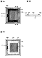
- FIG. 4A and 4B show a substrate used for manufacturing a capacitive sensor
- FIGS. 4C and 4D show a state in which a functional film is formed on the substrate
- FIGS. 4E and 4F show conductive portions and A mode that the insulation part was formed is shown.
- FIG. 5A and 5B show a state in which a routing wiring is formed
- FIG. 5C shows a state in which a decoration pattern is added to the substrate.
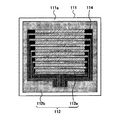
- FIG. 1 is a schematic diagram illustrating an outer shape of a capacitive sensor according to the present embodiment
- FIG. 2 is a schematic plan view illustrating an electrode configuration of the capacitive sensor according to the present embodiment
- FIG. 3 is a circuit block diagram of the capacitive sensor according to the present embodiment.
- the capacitive sensor 1 includes a sensor main body 11 and a flexible printed circuit board 12 connected to the outer periphery of the sensor main body 11.
- the sensor main body 11 includes a substrate 111 that forms the outer shape of the sensor main body 11.
- the substrate 111 is formed of a light-transmitting resin and is curved into a curved surface shape (FIG. 1).
- a plurality of conductive portions 112a functioning as detection electrodes of the capacitive sensor 1 are arranged in a stripe pattern on one main surface (a surface on the back side of the substrate 111 in FIG. 1) 111a of the substrate 111.
- the plurality of conductive portions 112a are all formed so that the planar shape is substantially rectangular, and are arranged substantially parallel to each other so that the distance between the adjacent conductive portions 112a is constant.
- Each conductive part 112a has conductivity and is insulated from each other by an insulating part 112b.
- the conductive portion 112a and the insulating portion 112b have a light-transmitting property so that a display of a display device (not shown) that is used in an overlapping manner with the capacitive sensor 1 can be visually recognized.
- a detected object such as a fingertip comes close to the conductive portion 112a, the capacitance of the conductive portion 112a changes. By utilizing this, the proximity position of the detection target can be specified.
- the plurality of conductive portions 112a and insulating portions 112b are configured by a single functional film 112.
- the conductive portion A step does not occur in the edge portion of 112a.
- the transmittance of the conductive portion 112a is not significantly reduced, and peeling from the edge portion of the conductive portion 112a can be prevented.
- the functional film 112 is formed using, for example, a conductive transparent resin such as PEDOT (polyethylenedioxythiophene).
- PEDOT polyethylenedioxythiophene
- PEDOT has a feature that it is insulated when it is overoxidized. Therefore, by partially peroxidizing the functional film 112 containing PEDOT, the conductive portion 112a and the insulating portion 112b can be separately formed without using a method such as etching.
- routing wiring 114 is connected to both ends of each conductive portion 112a.
- the other end of the routing wiring 114 is connected to a wiring (not shown) provided on the flexible printed circuit board 12.
- the flexible printed circuit board 12 is equipped with a detection IC 13 for detecting a change in the capacitance of the conductive portion 112a and a microprocessor 14 for processing a detection signal output from the detection IC 13.
- the change in the capacitance of the conductive portion 112a is detected as an electrical signal by the detection IC 13.
- the detection result of the detection IC 13 is input to the microprocessor 14 for signal processing.
- the signal processed by the microprocessor 14 is input to the external device 2 at the subsequent stage.
- the capacitance of the conductive portion 112a changes.
- the change in capacitance is greatest at the conductive portion 112a closest to the detection target in the arrangement direction of the conductive portions 112a (the direction perpendicular to the longitudinal direction of the conductive portions 112a).
- the change of the electrostatic capacitance of the plurality of conductive parts 112a is detected by the detection IC 13 and compared by the microprocessor 14, whereby the position of the detected object in the arrangement direction of the conductive parts 112a can be specified.
- the position of the detected object can be specified from the ratio of the change in capacitance of the two adjacent conductive parts 112a.
- the position of the detection object in the longitudinal direction of the conductive portion 112a is specified using the electrical resistance of the conductive portion 112a.
- Lead wires 114 are connected to both ends of the conductive portion 112a, respectively, and the capacitance of the conductive portion 112a can be detected from both ends. Since the conductive portion 112a has a predetermined electric resistance, the ratio of the detection amounts detected at both ends of the conductive portion 112a varies depending on the position of the detection target. For this reason, the position of the detected object can be specified based on the ratio of the detection amounts detected at both ends of the conductive portion 112a.
- the signal including the position information of the detection object output from the microprocessor 14 is arbitrarily used in the external device 2 at the subsequent stage.
- FIG. 4A is a schematic plan view showing a substrate 111 used for manufacturing the capacitive sensor 1
- FIG. 4B is a sectional view taken along the line IVB-IVB in FIG. 4A.
- a substrate 111 that constitutes the outer shape of the sensor body 11 is prepared.
- the substrate 111 is made of a light-transmitting resin such as PET, acrylic, or polycarbonate, and can be bent into a curved surface.
- the functional film 112 to be the conductive portion 112a and the insulating portion 112b is formed on the one-side main surface 111a of the substrate 111.
- 4C is a schematic plan view showing a state in which the functional film 112 is formed on the substrate 111.
- FIG. 4D is a cross-sectional view taken along the line IVD-IVD in FIG. 4C.
- the functional film 112 is formed by, for example, applying an aqueous solution of PEDOT / PSS (polyethylenedioxythiophene / polystyrene sulfonic acid).
- the functional film 112 containing PEDOT thus formed has both conductivity and translucency.
- PEDOT contained in the functional film 112 is represented by the following formula (1).
- FIG. 4E is a schematic plan view showing a state in which the conductive portion 112a and the insulating portion 112b are formed
- FIG. 4F is a cross-sectional view taken along the arrow IVF-IVF in FIG. 4E.
- a desired region of the functional film 112 is selectively peroxidized by, for example, a mask arrangement to form a plurality of conductive portions 112a and insulating portions 112b.
- the substrate 111 is in a state in which the single functional layer 112 having the plurality of conductive portions 112a and the insulating portions 112b is provided on the one-side main surface 111a.
- FIG. 5A is a schematic plan view showing a state in which the routing wiring 114 is formed
- FIG. 5B is a cross-sectional view taken along the line VB-VB in FIG. 5A.
- the routing wiring 114 is formed by a method such as screen printing or vapor deposition using a conductive material such as gold, silver, copper, aluminum, molybdenum, or carbon. Further, the routing wiring 114 is formed so that one end thereof is in contact with the conductive portion 112a and most of the remaining portion overlaps the insulating portion 112b.
- Each conductive portion 112a is provided with two routing wires 114 corresponding to both ends in the longitudinal direction of the conductive portion 112a.
- the two routing wirings 114 connected to both ends of each conductive portion 112a are formed so as to be substantially symmetric with respect to a straight line connecting the centers in the longitudinal direction of the plurality of conductive portions 112a. That is, the two routing wirings 114 are formed so as to be substantially line symmetrical with each other.
- the impedances of the two routing wires 114 connected to the single conductive portion 112a are substantially equal, and the capacitance can be detected from the both ends of the single conductive portion 112a under the same conditions. Even if the routing wiring 114 is asymmetric, by providing a difference in the conductivity of the conductive portion 112a and the routing wiring 114, the influence of the asymmetry when detecting the capacitance can be reduced.
- FIG. 5C is a schematic plan view showing a state in which the decoration pattern 115 is added to the substrate 111.
- the decoration pattern 115 is formed on the substrate 111 by a method such as screen printing.
- the routing pattern 114 formed on the substrate 111 is obscured by the decoration pattern 115.
- the processing of the surface of the substrate 111 is completed.
- the outer shape of the substrate 111 is then deformed by a method such as insert molding. Thereby, the sensor body 11 having an outer shape curved in a curved surface shape is realized (see FIG. 1).
- Each component such as the functional film 112 and the routing wiring 114 is curved together with the substrate 111.
- the flexible printed board 12 is connected to the sensor main body 11 through HC coating, outer shape processing, or the like (see FIG. 1).
- the capacitive sensor 1 including the single functional film 112 having the plurality of conductive portions 112a and the insulating portions 112b is manufactured.
- the plurality of conductive portions 112a and the insulating portion 112b that insulates the plurality of conductive portions 112a from each other are realized by a single functional film 112.
- the transmittance of the portion 112a is not significantly reduced as compared with other portions, and a uniform transmittance can be realized.
- the visibility of the display device that is used in an overlapping manner can be improved.
- peeling from the edge portion can be prevented and yield and productivity can be improved.
- the functional film 112 includes PEDOT (polyethylenedioxythiophene), so that the plurality of conductive portions 112a and the plurality of conductive portions 112a are insulated from each other.
- the insulating portion 112b to be formed can be appropriately formed by the single functional film 112.
- the substrate 111 since the substrate 111 has a curved surface shape together with the functional film 112, it is possible to realize a device with improved operational feeling and design.
- the plurality of conductive portions 112a and the insulating portion 112b that insulates the plurality of conductive portions 112a from each other are realized by a single functional film 112, even if the substrate 111 is curved into a curved shape, the conductive portions Peeling from the edge portion of 112a can be prevented.
- this invention is not limited to description of the said embodiment, It can implement by changing suitably in the aspect in which the effect is exhibited.
- the capacitive sensor in which the conductive portions are arranged in a stripe shape is shown, but the configuration of the conductive portions is not particularly limited.
- two layers of functional films may be provided so as to sandwich an insulating film therebetween, and the longitudinal directions of the conductive portions formed in the respective functional films may be crossed.
- the capacitance type sensor having a curved outer shape is shown, but the capacitance type sensor may have a flat outer shape. In this case, the step of deforming the outer shape of the substrate is not necessary.
- the capacitance type sensor in which the detection IC and the microprocessor are mounted on the flexible printed board is shown. However, the detection IC and the microprocessor may be mounted on the sensor body. Alternatively, it may be provided outside the capacitive sensor.
- the capacitive sensor of the present invention is useful as an input device that performs various inputs based on the contact position of a fingertip, for example.
Landscapes
- Engineering & Computer Science (AREA)
- General Engineering & Computer Science (AREA)
- Theoretical Computer Science (AREA)
- Human Computer Interaction (AREA)
- Physics & Mathematics (AREA)
- General Physics & Mathematics (AREA)
- Position Input By Displaying (AREA)
Description
本発明は、電極の静電容量変化に基づいて被検出体の位置検出を行う静電容量式センサに関する。
電極の静電容量変化に基づいて、指先などの被検出体の近接位置を2次元的に検出する静電容量式センサが提案されている(例えば、特許文献1参照)。この静電容量式センサは、第1軸方向に配列される第1電極と、第1電極と絶縁されて交差する第2電極とを備えている。この第1電極及び第2電極に被検出体が近接すると、静電容量は変化するので、静電容量の変化した第1電極と第2電極との組を検出することで、被検出体の近接位置を特定できる。
ところで、静電容量式センサは、液晶パネルなどの表示デバイスと重ねた状態で使用できるように、ある程度の透光性を要求される場合がある。このため、静電容量式センサには、ITO(酸化インジウムスズ)などの透明な導電膜をエッチングでパターン加工した透明電極が用いられている。
しかしながら、このようにパターン加工された透明電極の導電膜がある部分は、導電膜が除去された部分と比較して透過率が低くなるので、重ねて使用される表示デバイスの視認性が低下して文字入力や画面操作などに支障をきたす恐れがある。また、パターン加工で形成された透明電極のエッジ部分からピーリングが生じ、静電容量式センサの歩留まりや生産性が低下してしまう恐れもある。
本発明はかかる点に鑑みてなされたものであり、一様な透過率を実現すると共に、歩留まりや生産性を向上可能な静電容量式センサを提供することを目的とする。
本発明の静電容量式センサは、複数の導電部の静電容量の変化に基づいて被検出体の近接位置を検出する静電容量式センサであって、基板の片側主面に、前記複数の導電部と、前記複数の導電部を相互に絶縁する絶縁部と、を有する単一の機能膜が設けられたことを特徴とする。
この構成によれば、複数の導電部と、複数の導電部を相互に絶縁する絶縁部とを単一の機能膜で実現しているので、導電部の透過率が他の部分と比較して大幅に低下することはなくなり、一様な透過率を実現できる。また、導電部のエッジ部分に段差が生じないので、エッジ部分からのピーリングを防止でき、歩留まりや生産性を向上可能である。また、センサをフレキシブルな材料で構成した場合でも、変形に伴うピーリングを防止できる。
本発明の静電容量式センサにおいて、前記機能膜は、PEDOT(ポリエチレンジオキシチオフェン)を含んでいても良い。この構成によれば、複数の導電部と、複数の導電部を相互に絶縁する絶縁部とを、単一の機能膜により適切に形成できる。
本発明の静電容量式センサにおいて、前記基板は、前記機能膜と共に曲面形状を有しても良い。この構成によれば、基板が曲面形状を有するので、操作感やデザイン性を高めたデバイスを実現できる。また、複数の導電部と、複数の導電部を相互に絶縁する絶縁部とを単一の機能膜で実現しているので、基板が曲面形状に湾曲されても、導電部のエッジ部分からのピーリングを防止できる。
本発明によれば、一様な透過率を実現すると共に、歩留まりや生産性を向上可能な静電容量式センサを提供できる。
以下、添付図面を参照して、本発明の実施の形態に係る静電容量式センサの構成について説明する。なお、本実施の形態では説明の便宜上、簡略化された静電容量式センサについて説明するが、静電容量式センサに必要な構成は不足なく備えるものとする。また、各図においては、電極などの透明な構成を不透明に表現する場合がある。
図1は、本実施の形態に係る静電容量式センサの外形を示す模式図であり、図2は、本実施の形態に係る静電容量式センサの電極構成を示す平面模式図であり、図3は、本実施の形態に係る静電容量式センサの回路ブロック図である。図1に示すように、静電容量式センサ1は、センサ本体11と、センサ本体11の外周部に接続されたフレキシブルプリント基板12とを有している。
図1及び図2に示すように、センサ本体11は、センサ本体11の外形を構成する基板111を備えている。基板111は、透光性を有する樹脂で形成されており、曲面形状に湾曲されている(図1)。基板111の片側主面(図1における基板111の裏側の表面)111aには、静電容量式センサ1の検出用電極として機能する複数の導電部112aがストライプ状に配列されている。
複数の導電部112aは、いずれも平面形状が略長方形となるように形成されており、隣接する導電部112aとの間隔が一定となるように互いに略平行に配列されている。各導電部112aは、導電性を有し、絶縁部112bによって相互に絶縁されている。また、導電部112a及び絶縁部112bは透光性を有し、静電容量式センサ1と重ねて使用される表示デバイス(不図示)の表示を視認できるようになっている。この導電部112aに指先などの被検出体(不図示)が近接すると、導電部112aの静電容量は変化する。これを利用して、被検出体の近接位置を特定できる。
本実施の形態の静電容量式センサ1において、複数の導電部112a及び絶縁部112bは、単一の機能膜112で構成されている。このように、静電容量式センサ1の電極となる複数の導電部112aと、複数の導電部112aを相互に絶縁する絶縁部112bとを単一の機能膜112で実現することにより、導電部112aのエッジ部分に段差が生じることはなくなる。このため、エッチングでパターン加工する場合のように、導電部112aの透過率が大幅に低下することはなく、また、導電部112aのエッジ部分からのピーリングも防止できる。
機能膜112は、例えば、PEDOT(ポリエチレンジオキシチオフェン)などの導電性を有する透明樹脂を用いて形成される。PEDOTは、過酸化処理されると絶縁化されるという特徴を有している。このため、PEDOTを含有する機能膜112を、部分的に過酸化することで、エッチングなどの方法を用いることなく、導電部112aと絶縁部112bとを作り分けることができる。
各導電部112aの両端部には、それぞれ、引き回し用配線114の一端部が接続されている。引き回し用配線114の他端部は、フレキシブルプリント基板12に設けられた配線(不図示)と接続されている。フレキシブルプリント基板12には、導電部112aの静電容量の変化を検出する検出用IC13、及び検出用IC13から出力される検出信号を処理するマイクロプロセッサ14が搭載されている。
図3に示すように、導電部112aの静電容量の変化は、検出用IC13で電気信号として検出される。検出用IC13の検出結果は、マイクロプロセッサ14に入力されて信号処理される。マイクロプロセッサ14で処理された信号は、後段の外部装置2に入力される。
この静電容量式センサ1のセンサ本体11に、指先などの被検出体が近接すると、導電部112aの静電容量は変化する。静電容量の変化は、導電部112aの配列方向(導電部112aの長手方向に垂直な方向)において、被検出体に最も近い導電部112aで最大となる。このため、複数の導電部112aの静電容量の変化を検出用IC13で検出し、マイクロプロセッサ14で比較することにより、導電部112aの配列方向における被検出体の位置を特定できる。例えば、隣接する2本の導電部112aの間に被検出体が位置付けられる場合には、隣接する2本の導電部112aの静電容量の変化の比から被検出体の位置を特定できる。
一方、導電部112aの長手方向における被検出体の位置は、導電部112aの電気抵抗を利用して特定される。導電部112aの両端部には、それぞれ、引き回し用配線114が接続されており、導電部112aの静電容量は、両端部のいずれからも検出できるようになっている。導電部112aは所定の電気抵抗を有しているので、導電部112aの両端部でそれぞれ検出される検出量の比は、被検出体の位置に応じて変化する。このため、導電部112aの両端部で検出される検出量の比に基づいて、被検出体の位置を特定できる。マイクロプロセッサ14から出力される被検出体の位置情報を含む信号は、後段の外部装置2で任意に利用される。
図4及び図5を参照して、本実施の形態に係る静電容量式センサ1の製造方法を説明する。図4Aは、静電容量式センサ1の製造に用いられる基板111を示す平面模式図であり、図4Bは、図4AのIVB-IVB矢視断面図である。図4A及び図4Bに示すように、本実施の形態に係る静電容量式センサの製造方法では、まず、センサ本体11の外形を構成する基板111を用意する。基板111は、例えば、PET、アクリル、ポリカーボネートなどの透光性を有する樹脂によって形成されており、曲面形状に湾曲可能となっている。
この基板111の片側主面111aに、導電部112a及び絶縁部112bとなる機能膜112を形成する。図4Cは、基板111に機能膜112が形成された様子を示す平面模式図であり、図4Dは、図4CのIVD-IVD矢視断面図である。機能膜112は、例えば、PEDOT/PSS(ポリエチレンジオキシチオフェン/ポリスチレンスルフォン酸)の水溶液を塗布することで形成される。このようにして形成されるPEDOTを含有する機能膜112は、導電性と透光性とを併せ備えている。
ここで、機能膜112に含有されるPEDOTは、下記式(1)で表される。

このPEDOTを過酸化すると、下記式(2)のようなチオフェン環の開環反応が生じて絶縁化される。このため、PEDOTを含有する機能膜112を過酸化することにより、機能膜112を絶縁化できる。

図4Eは、導電部112a及び絶縁部112bが形成された様子を示す平面模式図であり、図4Fは、図4EのIVF-IVF矢視断面図である。基板111の片側主面111aに機能膜112が形成された後には、機能膜112の所望領域を、例えば、マスク配置により選択的に過酸化させ、複数の導電部112a及び絶縁部112bを形成する。これにより、基板111は、複数の導電部112a及び絶縁部112bを有する単一の機能層112が片側主面111aに設けられた状態となる。
次に、導電部112aと接続される引き回し用配線114を形成する。図5Aは、引き回し用配線114が形成された様子を示す平面模式図であり、図5Bは、図5AのVB-VB矢視断面図である。引き回し用配線114は、例えば、金、銀、銅、アルミニウム、モリブデン、カーボンなどの導電性材料を用いて、スクリーン印刷、蒸着などの方法で形成される。また、引き回し用配線114は、一端が導電部112aと接触し、残りの大部分は絶縁部112bと重なるように形成される。
各導電部112aには、導電部112aの長手方向の両端部に対応して、それぞれ2本の引き回し用配線114が設けられる。各導電部112aの両端部に接続される2本の引き回し用配線114は、複数の導電部112aの長手方向の中心を結ぶ直線に対して略対称となるように形成される。つまり、2本の引き回し用配線114は、互いに略線対称となるように形成される。その結果、1本の導電部112aに接続される2本の引き回し用配線114のインピーダンスは略等しくなり、1本の導電部112aの両端部から同じ条件で静電容量を検出できる。なお、引き回し用配線114が非対称であっても、導電部112aや引き回し用配線114の導電性に差を設けることで、静電容量を検出する際の非対称の影響を小さくできる。
その後、基板111の引き回し用配線114が形成された領域を加飾する。図5Cは、基板111に加飾パターン115が追加された様子を示す平面模式図である。この工程では、スクリーン印刷などの方法で基板111に加飾パターン115が形成される。加飾パターン115により、基板111に形成された引き回し用配線114は覆い隠される。以上により、基板111の表面の加工が終了する。
基板111の表面の加工が終了すると、次に、インサート成形などの方法で基板111の外形を変形させる。これにより、曲面状に湾曲された外形形状を有するセンサ本体11が実現される(図1参照)。機能膜112や引き回し用配線114などの各構成は、基板111と共に湾曲される。
センサ本体11の外形形状が形成された後には、HC塗工や外形加工など経て、センサ本体11にフレキシブルプリント基板12が接続される(図1参照)。以上の工程により、複数の導電部112aと絶縁部112bとを有する単一の機能膜112を備えた静電容量式センサ1が製造される。
本実施の形態に係る静電容量式センサ1は、複数の導電部112aと、複数の導電部112aを相互に絶縁する絶縁部112bとを単一の機能膜112で実現しているので、導電部112aの透過率が他の部分と比較して大幅に低下することはなくなり、一様な透過率を実現できる。その結果、重ねて使用される表示デバイスの視認性を高めることができる。また、導電部112aのエッジ部分に段差が生じないので、エッジ部分からのピーリングを防止して歩留まりや生産性を向上可能である。
また、本実施の形態に係る静電容量式センサ1において、機能膜112は、PEDOT(ポリエチレンジオキシチオフェン)を含んでいるので、複数の導電部112aと、複数の導電部112aを相互に絶縁する絶縁部112bとを、単一の機能膜112により適切に形成できる。
また、本実施の形態に係る静電容量式センサ1において、基板111は、機能膜112と共に曲面形状を有しているので、操作感やデザイン性を高めたデバイスを実現できる。また、複数の導電部112aと、複数の導電部112aを相互に絶縁する絶縁部112bとを単一の機能膜112で実現しているので、基板111が曲面形状に湾曲されても、導電部112aのエッジ部分からのピーリングを防止できる。
なお、本発明は上記実施の形態の記載に限定されず、その効果が発揮される態様で適宜変更して実施できる。例えば、上記実施の形態においては、導電部がストライプ状に配列された静電容量式センサを示したが、導電部の構成は特に限定されない。例えば、絶縁膜を間に挟むように2層の機能膜を設け、各機能膜に形成される導電部の長手方向が交差するようにしても良い。
また、上記実施の形態においては、湾曲された外形形状を有する静電容量式センサを示しているが、静電容量式センサは平坦な外形を有していても良い。この場合、基板の外形を変形させる工程は不要となる。また、上記実施の形態においては、フレキシブルプリント基板に検出用IC及びマイクロプロセッサが搭載された静電容量式センサを示しているが、検出用IC及びマイクロプロセッサはセンサ本体に実装されても良いし、静電容量式センサの外部に設けられても良い。
本発明の静電容量式センサは、例えば、指先などの接触位置に基づいて各種入力を行う入力デバイスとして有用である。
1 静電容量式センサ
2 外部装置
11 センサ本体
12 フレキシブルプリント基板
13 検出用IC
14 マイクロプロセッサ
111 基板
111a 片側主面
112 機能膜
112a 導電部
112b 絶縁部
114 引き回し用配線
115 加飾パターン
2 外部装置
11 センサ本体
12 フレキシブルプリント基板
13 検出用IC
14 マイクロプロセッサ
111 基板
111a 片側主面
112 機能膜
112a 導電部
112b 絶縁部
114 引き回し用配線
115 加飾パターン
Claims (3)
- 複数の導電部の静電容量の変化に基づいて被検出体の近接位置を検出する静電容量式センサであって、
基板の片側主面に、前記複数の導電部と、前記複数の導電部を相互に絶縁する絶縁部と、を有する単一の機能膜が設けられたことを特徴とする静電容量式センサ。 - 前記機能膜は、PEDOT(ポリエチレンジオキシチオフェン)を含むことを特徴とする請求項1記載の静電容量式センサ。
- 前記基板は、前記機能膜と共に曲面形状を有することを特徴とする請求項1又は請求項2記載の静電容量式センサ。
Applications Claiming Priority (2)
| Application Number | Priority Date | Filing Date | Title |
|---|---|---|---|
| JP2012205875A JP2015222456A (ja) | 2012-09-19 | 2012-09-19 | 静電容量式センサ |
| JP2012-205875 | 2012-09-19 |
Publications (1)
| Publication Number | Publication Date |
|---|---|
| WO2014045562A1 true WO2014045562A1 (ja) | 2014-03-27 |
Family
ID=50340902
Family Applications (1)
| Application Number | Title | Priority Date | Filing Date |
|---|---|---|---|
| PCT/JP2013/005474 Ceased WO2014045562A1 (ja) | 2012-09-19 | 2013-09-17 | 静電容量式センサ |
Country Status (2)
| Country | Link |
|---|---|
| JP (1) | JP2015222456A (ja) |
| WO (1) | WO2014045562A1 (ja) |
Cited By (4)
| Publication number | Priority date | Publication date | Assignee | Title |
|---|---|---|---|---|
| WO2016152518A1 (ja) * | 2015-03-25 | 2016-09-29 | アルプス電気株式会社 | 配線基板、配線基板の製造方法、及び配線基板を備えた静電容量センサ |
| JP2017102769A (ja) * | 2015-12-03 | 2017-06-08 | Smk株式会社 | タッチセンサ、タッチパネルおよび電子機器 |
| JP2017102770A (ja) * | 2015-12-03 | 2017-06-08 | Smk株式会社 | タッチセンサ、タッチパネルおよび電子機器 |
| US10857390B2 (en) | 2015-10-16 | 2020-12-08 | Dalhousie University | Systems and methods for monitoring patient motion via capacitive position sensing |
Families Citing this family (1)
| Publication number | Priority date | Publication date | Assignee | Title |
|---|---|---|---|---|
| JP6620058B2 (ja) * | 2016-04-04 | 2019-12-11 | 株式会社ジャパンディスプレイ | 表示装置 |
Citations (3)
| Publication number | Priority date | Publication date | Assignee | Title |
|---|---|---|---|---|
| JP2008097283A (ja) * | 2006-10-11 | 2008-04-24 | Hosiden Corp | タッチパネル入力装置 |
| JP2009211680A (ja) * | 2008-02-08 | 2009-09-17 | Fujitsu Component Ltd | パネル型入力装置、パネル型入力装置の製造方法、及びパネル型入力装置を備えた電子機器 |
| JP2010244772A (ja) * | 2009-04-03 | 2010-10-28 | Sony Corp | 静電容量式タッチ部材及びその製造方法、並びに静電容量式タッチ検出装置 |
-
2012
- 2012-09-19 JP JP2012205875A patent/JP2015222456A/ja active Pending
-
2013
- 2013-09-17 WO PCT/JP2013/005474 patent/WO2014045562A1/ja not_active Ceased
Patent Citations (3)
| Publication number | Priority date | Publication date | Assignee | Title |
|---|---|---|---|---|
| JP2008097283A (ja) * | 2006-10-11 | 2008-04-24 | Hosiden Corp | タッチパネル入力装置 |
| JP2009211680A (ja) * | 2008-02-08 | 2009-09-17 | Fujitsu Component Ltd | パネル型入力装置、パネル型入力装置の製造方法、及びパネル型入力装置を備えた電子機器 |
| JP2010244772A (ja) * | 2009-04-03 | 2010-10-28 | Sony Corp | 静電容量式タッチ部材及びその製造方法、並びに静電容量式タッチ検出装置 |
Cited By (8)
| Publication number | Priority date | Publication date | Assignee | Title |
|---|---|---|---|---|
| WO2016152518A1 (ja) * | 2015-03-25 | 2016-09-29 | アルプス電気株式会社 | 配線基板、配線基板の製造方法、及び配線基板を備えた静電容量センサ |
| JPWO2016152518A1 (ja) * | 2015-03-25 | 2017-08-10 | アルプス電気株式会社 | 配線基板、配線基板の製造方法、及び配線基板を備えた静電容量センサ |
| US10857390B2 (en) | 2015-10-16 | 2020-12-08 | Dalhousie University | Systems and methods for monitoring patient motion via capacitive position sensing |
| US11612763B2 (en) | 2015-10-16 | 2023-03-28 | Dalhousie University | Systems and methods for monitoring patient motion via capacitive position sensing |
| US11911632B2 (en) | 2015-10-16 | 2024-02-27 | Dalhousie University | Systems and methods for monitoring patient motion via capacitive position sensing |
| JP2017102769A (ja) * | 2015-12-03 | 2017-06-08 | Smk株式会社 | タッチセンサ、タッチパネルおよび電子機器 |
| JP2017102770A (ja) * | 2015-12-03 | 2017-06-08 | Smk株式会社 | タッチセンサ、タッチパネルおよび電子機器 |
| US9992872B2 (en) | 2015-12-03 | 2018-06-05 | Smk Corporation | Touch sensor, touch panel, and electronic device |
Also Published As
| Publication number | Publication date |
|---|---|
| JP2015222456A (ja) | 2015-12-10 |
Similar Documents
| Publication | Publication Date | Title |
|---|---|---|
| TWI664560B (zh) | 層疊構造體、觸摸面板、帶觸摸面板的顯示裝置及其製造方法 | |
| CN102449582B (zh) | 静电容量方式输入装置 | |
| CN101553776B (zh) | 触摸面板装置及其制造方法 | |
| US8698001B2 (en) | Electrode structure of the touch panel, method thereof and touch panel | |
| US20140347319A1 (en) | Touch panel | |
| KR102316212B1 (ko) | 터치 센서 및 이의 제조 방법 | |
| TWI475461B (zh) | Electrostatic Capacitive Input Device | |
| US20130256008A1 (en) | Touch panel and method for manufacturing a touch sensor layer of the touch panel | |
| KR102264037B1 (ko) | 투명 전극 패턴, 그 제조 방법 및 이를 포함한 터치 센서 | |
| US20140152588A1 (en) | Flexible touch screen panel and fabricating method thereof | |
| US10248268B2 (en) | OGS capacitive touch screen and manufacturing method thereof | |
| JP5520162B2 (ja) | 入力装置及びその製造方法 | |
| CN112654954B (zh) | 触控面板及其制作方法、电子装置 | |
| JP5846953B2 (ja) | 入力装置及びその製造方法 | |
| WO2014045562A1 (ja) | 静電容量式センサ | |
| US8780067B1 (en) | Bridging structure for signal transmission of touch panel | |
| WO2014015618A1 (zh) | 触控面板及其制造方法、触控设备 | |
| JP2014178718A (ja) | タッチパネルおよびタッチパネル付き表示装置 | |
| KR20120111986A (ko) | 입력 장치 및 그 제조 방법 | |
| JP5878593B2 (ja) | 入力装置の製造方法 | |
| KR20160133603A (ko) | 터치 스크린 패널 | |
| WO2017183315A1 (ja) | 静電容量式センサ | |
| KR101320525B1 (ko) | 터치패널 및 그 제조방법 | |
| WO2014045541A1 (ja) | 静電容量式センサ | |
| JP2011186977A (ja) | 入力装置の製造方法 |
Legal Events
| Date | Code | Title | Description |
|---|---|---|---|
| 121 | Ep: the epo has been informed by wipo that ep was designated in this application |
Ref document number: 13840055 Country of ref document: EP Kind code of ref document: A1 |
|
| NENP | Non-entry into the national phase |
Ref country code: DE |
|
| 122 | Ep: pct application non-entry in european phase |
Ref document number: 13840055 Country of ref document: EP Kind code of ref document: A1 |
|
| NENP | Non-entry into the national phase |
Ref country code: JP |