WO2014045486A1 - シート伝送システム、電磁波伝播シート及び近接カプラ - Google Patents
シート伝送システム、電磁波伝播シート及び近接カプラ Download PDFInfo
- Publication number
- WO2014045486A1 WO2014045486A1 PCT/JP2013/002540 JP2013002540W WO2014045486A1 WO 2014045486 A1 WO2014045486 A1 WO 2014045486A1 JP 2013002540 W JP2013002540 W JP 2013002540W WO 2014045486 A1 WO2014045486 A1 WO 2014045486A1
- Authority
- WO
- WIPO (PCT)
- Prior art keywords
- dielectric
- sheet
- electromagnetic wave
- wave propagation
- transmission system
- Prior art date
- Legal status (The legal status is an assumption and is not a legal conclusion. Google has not performed a legal analysis and makes no representation as to the accuracy of the status listed.)
- Ceased
Links
Images





Classifications
-
- H—ELECTRICITY
- H04—ELECTRIC COMMUNICATION TECHNIQUE
- H04B—TRANSMISSION
- H04B13/00—Transmission systems characterised by the medium used for transmission, not provided for in groups H04B3/00 - H04B11/00
-
- H—ELECTRICITY
- H04—ELECTRIC COMMUNICATION TECHNIQUE
- H04B—TRANSMISSION
- H04B5/00—Near-field transmission systems, e.g. inductive or capacitive transmission systems
- H04B5/70—Near-field transmission systems, e.g. inductive or capacitive transmission systems specially adapted for specific purposes
- H04B5/79—Near-field transmission systems, e.g. inductive or capacitive transmission systems specially adapted for specific purposes for data transfer in combination with power transfer
Definitions
- the present invention relates to a sheet transmission system that transmits electromagnetic waves, an electromagnetic wave propagation sheet, and a proximity coupler.
- a two-dimensional communication system has been proposed as a system for performing communication between electronic devices via a sheet-like medium.
- the two-dimensional communication system includes an electromagnetic wave propagation sheet and a proximity coupler.
- the proximity coupler is an electromagnetic coupling device that inputs and outputs electromagnetic waves with the inside of the sheet using an electromagnetic field that oozes from the surface of the electromagnetic wave propagation sheet.
- Patent Document 1 A two-dimensional communication system including an electromagnetic wave propagation sheet and a proximity coupler is disclosed in Patent Document 1, Non-Patent Document 1, Non-Patent Document 2, and the like.
- FIG. 11 shows a cross-sectional view of a state in which a proximity coupler is placed on the electromagnetic wave propagation sheet.
- two conductor layers (mesh-shaped conductor 13 and plain-shaped conductor 12) are arranged on both surfaces of a dielectric (communication layer) 11.
- a dielectric (protective layer) 14 that protects the mesh-shaped conductor 13 is provided on the mesh-shaped conductor 13.
- the electromagnetic wave propagating inside the electromagnetic wave propagation sheet 10, that is, between the mesh-shaped conductor 13 and the plain-shaped conductor 12 oozes out from the opening of the mesh-shaped conductor 13.
- communication is realized between electronic devices placed on the sheet via the oozed electromagnetic waves.
- This technology can be applied not only to communication but also to power transmission.
- high frequency AC power is injected into the seat from a power feeding coupler connected to a high frequency power supply.
- the proximity coupler for power reception absorbs the electromagnetic wave which oozes out from the sheet surface, converts it into direct current by a rectifier circuit, and supplies electric power to the electronic device.
- Patent 4538594 (FIGS. 1 and 9)
- the electromagnetic wave propagation sheet has a small dielectric constant of the protective layer, and the dielectric of the proximity coupler uses the same dielectric as the protective layer. For this reason, the wavelength shortening effect cannot be greatly obtained as compared with the case where a material having a high dielectric constant is used, and the size of the proximity coupler is increased. For example, such a proximity coupler is not suitable for use in a portable terminal.
- the present invention has been made to solve such problems, and an object of the present invention is to provide a sheet transmission system, an electromagnetic wave propagation sheet, and a proximity coupler that can reduce the size of the proximity coupler.
- a sheet transmission system includes an electromagnetic wave propagation sheet having a protective layer made of a dielectric, a proximity coupler that transmits electromagnetic waves between the electromagnetic wave propagation sheet, the electromagnetic wave propagation sheet, and the proximity
- the coupler includes a first dielectric that is provided between a conductor having a feeding point and has a dielectric constant greater than that of the protective layer.
- An electromagnetic wave propagation sheet is an electromagnetic wave propagation sheet having a protective layer made of a dielectric material and transmitting electromagnetic waves to and from a proximity coupler, wherein the protection layer is disposed on the uppermost layer on the proximity coupler side.
- a first dielectric layer having a dielectric constant larger than that of the layer is provided.
- a proximity coupler includes a plane-shaped conductor provided with a slot, and a patch conductor provided via the plane-shaped conductor and a dielectric, and electromagnetic waves are transmitted between the electromagnetic wave propagation sheet.
- the present invention it is possible to provide a sheet transmission system, an electromagnetic wave propagation sheet, and a proximity coupler that can reduce the size of the proximity coupler.
- Embodiment 1 of the Invention In the sheet transmission system according to the embodiment of the present invention, the electromagnetic wave propagation sheet is disposed between the electromagnetic wave propagation sheet and a conductor having a feeding point in the proximity coupler (typically, between the electromagnetic wave propagation sheet and the proximity coupler). Install a dielectric with a dielectric constant greater than that of the protective layer.
- the dielectric is placed between the electromagnetic wave propagation sheet and a conductor having a feeding point in the proximity coupler (between the electromagnetic wave propagation sheet and the proximity coupler), thereby Since the effective dielectric constant of the structure between the plane-shaped conductor and the mesh-shaped conductor of the electromagnetic wave propagation sheet, which determines the resonance frequency, increases, the resonance frequency of the proximity coupler shifts to the low frequency side. As a result, the size of the proximity coupler can be reduced.
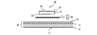
- FIG. 1 shows a configuration of a sheet transmission system according to the first embodiment.
- the sheet transmission system includes an electromagnetic wave propagation sheet 10, a proximity coupler 20, and a dielectric 30.
- the dielectric 30 is provided between the electromagnetic wave propagation sheet 10 and the proximity coupler 20.
- the electromagnetic wave propagation sheet 10 is a plate-like sheet having a rectangular plan view.
- the electromagnetic wave propagation sheet 10 may have rigidity or bendable.
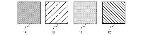
- the electromagnetic wave propagation sheet 10 includes a communication layer 11, a plain-shaped conductor 12, a mesh-shaped conductor 13, and a protective layer 14.
- the communication layer 11, the plain-shaped conductor 12, the mesh-shaped conductor 13, and the protective layer 14 are all sheet-like.
- the “sheet shape” means a state having a two-dimensional spread as a surface and a small thickness. Examples of the sheet shape include a cloth shape, a paper shape, a foil shape, a plate shape, a film shape, a film shape, and a mesh shape.
- FIG. 2 shows an exploded plan view of the electromagnetic wave propagation sheet 10.
- the communication layer 11 is made of a dielectric material.
- the communication layer 11 is sandwiched between a plain-shaped conductor 12 and a mesh-shaped conductor 13.
- the material of the communication layer 11 is selected according to the purpose of use of the electromagnetic wave propagation sheet 10 or the like.
- resin, rubber, a polymer foam, a gel material, or the like can be used as the communication layer 11.
- the plane-shaped conductor 12 is a surface conductor layer provided so as to extend uniformly over the entire lower surface of the communication layer 11.
- the plain-shaped conductor 12 is configured by, for example, a metal foil or a metal plate such as copper or aluminum.
- the mesh conductor 13 is a back conductor layer having a square mesh structure, for example.
- the repeating unit of the mesh is equal to the distance between the centers of the horizontally adjacent squares.
- the repeating unit dimension of the mesh is sufficiently shorter than the electromagnetic wave length of the communication layer 11.
- the “mesh shape” refers to a state in which a plurality of openings having a regular or irregular shape are formed in addition to a regular mesh.
- a lattice pattern in which the shape of the opening is rectangular is typical, but as the shape of the opening, various shapes such as a turtle shell shape, a rhombus, a circle, and a triangle can be used.
- the mesh-shaped conductor 13 can be manufactured by etching a thin plate of metal (for example, aluminum), and the mesh-shaped portion may be patterned at the time of manufacturing.
- An electromagnetic wave called an evanescent wave oozes out from the mesh-shaped conductor 13, so that an electromagnetic wave leaching region is formed above the mesh-shaped conductor 13.
- the plane-shaped conductor 12 and the mesh-shaped conductor 13 are arranged in a substantially parallel state, and electromagnetic waves travel through a space between the plane-shaped conductor 12 and the mesh-shaped conductor 13.
- electromagnetic waves travel through the communication layer 11.
- the protective layer 14 is a dielectric provided so as to cover the entire upper surface (the surface opposite to the communication layer 11) of the mesh-shaped conductor 13.
- the protective layer 14 is provided to prevent the mesh-shaped conductor 13 from being damaged by an external force.
- resin, rubber, a polymer foam, a gel material, a hollow structure, or the like can be used as the protective layer 14.
- a device for sending an electromagnetic wave to the electromagnetic wave propagation sheet 10 is attached to an end portion in the longitudinal direction of the electromagnetic wave propagation sheet 10 so that communication or power feeding with the proximity coupler 20 placed on the electromagnetic wave propagation sheet 10 is performed. Is called.
- An apparatus for sending electromagnetic waves may be placed on the electromagnetic wave propagation sheet 10.
- the proximity coupler 20 is a coupler type power receiving device including a dielectric 21 and two conductor layers (plane-shaped conductor 22 and patch conductor 23) provided on both surfaces thereof.
- the proximity coupler 20 is an interface device that is used by being placed on the electromagnetic wave propagation sheet 10, and transmits and receives electromagnetic waves to and from the electromagnetic wave propagation sheet 10.
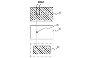
- FIG. 3 is an exploded plan view of the proximity coupler 20.
- the dielectric 21 for example, resin, rubber, polymer foam, gel material, or the like can be used.
- the dielectric 21 of the proximity coupler 20 may be made of the same material as the protective layer 14 of the electromagnetic wave propagation sheet 10. In this case, the dielectric constants of the dielectric 21 and the protective layer 14 are the same.
- the plane-shaped conductor 22 has a feeding point and has a planar shape that covers the entire top surface of the dielectric 21. Further, the plane-shaped conductor 22 has a slot 24 in which a part thereof is cut out in an elongated rectangular shape. As shown in FIG. 3, the position of the slot 24 of the plane-shaped conductor 25 is located inside the patch conductor, and has a shape that allows impedance matching at the feeding point. The feed point is placed on the portion of the conductor at both ends of the slot.
- the plain-shaped conductor 22 is made of, for example, a metal foil or a metal plate such as copper or aluminum.
- the patch conductor 23 has a planar shape that covers a part of the lower surface of the dielectric 21 near the center.
- the term “patch” means a small piece or a fragment, and a plate-like microstrip antenna is generally called “patch antenna”. It is a term used.
- the length of the patch conductor 23 in the longitudinal direction is set so as to resonate at the frequency of the electromagnetic wave propagating through the electromagnetic wave propagation sheet 10 when the proximity coupler 20 is placed on the electromagnetic wave propagation sheet 10.
- the patch conductor 23 is made of, for example, a metal foil or a metal plate such as copper or aluminum.
- the plane-shaped conductor 22 is provided on the upper surface of the printed circuit board, and the patch conductor 23 is provided on the lower surface of the printed circuit board. Further, it is also possible to realize by using a conductor layer of a printed board as the plane-shaped conductor 22 and using a copper plate different from the printed board for the patch conductor 23 and bonding them to both surfaces of the dielectric.
- the independent potential feeding point formed on the plane-shaped conductor 22 and the patch conductor 23 are electrically connected by the conductor 25.
- the position of the conductor 25 is set to a position where impedance matching can be obtained at the feeding point.
- the length of the patch conductor 23 is set so as to resonate at the frequency of the electromagnetic wave propagating through the electromagnetic wave propagation sheet 10 when the proximity coupler 20 is placed on the electromagnetic wave propagation sheet 10.
- the configuration shown in FIGS. 4 and 5 is realized by, for example, a printed circuit board.
- the proximity coupler 20 has a flat plate shape, but may be configured to be bendable.
- a dielectric 30 having a dielectric constant higher than that of the protective layer 14 of the electromagnetic wave propagation sheet 10 is provided between the electromagnetic wave propagation sheet 10 and the proximity coupler 20.
- the dielectric 30 does not have to be a flat plate, and may have a wavy shape or a concavo-convex shape.
- the dielectric 30 may have a hole in a part thereof.
- the dielectric constant of the protective layer of the electromagnetic wave propagation sheet is set to be small as in the power transmission system disclosed in Non-Patent Document 2, the effect of shortening the wavelength is great.
- the size of the patch conductor 23 can be reduced as compared with the case where there is no dielectric as shown in the related art, and the proximity coupler 20 is small. Can be realized. Therefore, compared to the sheet transmission system disclosed in the related art, it is possible to realize the proximity coupler 20 that is suitable for being incorporated in a portable terminal.
- the dielectric 30 is preferably larger in size than the patch conductor 23. The reason is that since the electric field between the patch conductor 23 and the mesh-shaped conductor 13 of the electromagnetic wave propagation sheet 10 spreads in a range larger than the size of the patch conductor 23, the effective dielectric constant is larger when the patch conductor 23 is larger than the size. It is to become.
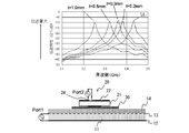
- FIG. 6 shows an actual measurement result performed for confirming the effect exhibited by the sheet transmission system according to the present embodiment.
- a dielectric 30 is installed between the electromagnetic wave propagation sheet 10 and the proximity coupler 20.
- a feeding point (Port 1) is provided between the mesh-shaped conductor 13 and the plain-shaped conductor 12.
- feed points (Port 2) are provided on both sides of the slot 24 of the plain-shaped conductor 22 of the proximity coupler 20.
- the slot 24 has a shape that is long in the direction perpendicular to the paper surface. Then, each feeding point was connected to a network analyzer, and the transmission characteristic S21 was measured.
- the electromagnetic wave propagation sheet is designed to prevent standing waves.
- the dielectric 21 of the proximity coupler 20 and the protective layer 14 of the electromagnetic wave propagation sheet 10 have a relative dielectric constant of 1.17 and a thickness of 4 mm.
- the dielectric 30 has a relative dielectric constant of 2.6 and a dielectric loss tangent (tan ⁇ ) of 0.003.
- the relative dielectric constant of the dielectric (communication layer) 11 between the mesh-shaped conductor 13 and the plain-shaped conductor 12 is 2.1 and the thickness is 1 mm.
- the result of measuring the transmission characteristics by changing the thickness t of the dielectric 30 is the graph shown in the upper part of FIG.
- the resonant frequency (frequency at which the transmission amount shows a peak) is shifted to the low frequency side by installing.
- the resonant frequency is gradually shifted to the low frequency side by increasing the thickness t of the dielectric 30 from 0.2 mm to 0.3 mm, 0.5 mm, and 1.0 mm in stages.
- FIG. 7 is a diagram illustrating a configuration of the sheet transmission system according to the second embodiment.
- the sheet transmission system according to the first exemplary embodiment of the present invention is that the dielectric 30 is not a single layer but has a structure in which a dielectric 31 and a dielectric 32 having different dielectric constants are stacked in a plurality of layers. Different. Other configurations are the same as those of the first embodiment.
- the dielectric 31 and the dielectric 32 are both sheet-like dielectric layers.
- the dielectric constant of the dielectric 31 and the dielectric 32 may be larger than that of the dielectric 32 or vice versa.
- the dielectric constants of the dielectric 31 and the dielectric 32 are both higher than that of the protective layer 14 of the electromagnetic wave propagation sheet 10.
- the dielectric 30 need not be two layers of the dielectric 31 and the dielectric 32, and may have a multilayer structure of three or more layers.
- the dielectrics 31 and 32 having a dielectric constant higher than that of the protective layer 14 of the electromagnetic wave propagation sheet 10 are installed between the electromagnetic wave propagation sheet 10 and the proximity coupler 20.
- the resonance frequency can be lowered, and the proximity coupler 20 can be reduced in size.
- FIG. 8 is a diagram illustrating a configuration of a sheet transmission system according to the third embodiment.
- the sheet transmission system according to the first embodiment of the present invention is different from the sheet transmission system according to the first embodiment in that the dielectric 33 forms a casing of an electronic device in which the proximity coupler 20 is built.
- Other configurations are the same as those of the first embodiment.
- the dielectric 33 has a dielectric constant higher than that of the protective layer 14 of the electromagnetic wave propagation sheet 10.
- the dielectric 33 shown in FIG. 8 is a box containing the entire electronic component including the proximity coupler 20 as a housing of the electronic device.
- the entire casing is integrally formed of the dielectric 33 made of the same material.
- the dielectric 33 having a higher dielectric constant than the protective layer 14 of the sheet 10 may be used.
- the dielectric 33 may not be a single layer but a plurality of layers.
- the dielectric 33 having a dielectric constant higher than that of the protective layer 14 of the electromagnetic wave propagation sheet 10 is provided between the electromagnetic wave propagation sheet 10 and the proximity coupler 20, resonance occurs.
- the frequency can be lowered, and the proximity coupler 20 can be reduced in size.
- the dielectric 33 constitutes the casing of the electronic device in which the proximity coupler 20 is built, the electronic device itself is smaller than the case where a dielectric is provided in addition to the casing. In addition, the number of parts can be reduced.
- FIG. 9 is a diagram illustrating a configuration of a sheet transmission system according to the fourth embodiment.
- the sheet transmission system according to the first embodiment of the present invention is different in that the dielectric 34 is integrated with the electromagnetic wave propagation sheet 10.
- Other configurations are the same as those of the first embodiment.
- the dielectric 34 is a sheet-like dielectric layer having the same shape as that of the electromagnetic wave propagation sheet 10 in a plan view.
- the dielectric 34 abuts on the outer surface (upper surface) of the protective layer 14 of the electromagnetic wave propagation sheet 10 and is located on the uppermost layer on the proximity coupler 20 side.
- the dielectric 34 has a higher dielectric constant than the protective layer 14 of the electromagnetic wave propagation sheet 10.
- the dielectric 34 may not be a single layer but a plurality of layers.
- the dielectric 34 having a dielectric constant higher than that of the protective layer 14 of the electromagnetic wave propagation sheet 10 is disposed between the electromagnetic wave propagation sheet 10 and the proximity coupler 20, resonance occurs.
- the frequency can be lowered, and the proximity coupler 20 can be reduced in size.
- the dielectric 34 is formed integrally with the electromagnetic wave propagation sheet 10, it is easy to handle and can reliably cover the entire upper surface of the electromagnetic wave propagation sheet 10.
- the resonance frequency can be lowered uniformly and accurately over the entire surface of the electromagnetic wave propagation sheet 10.
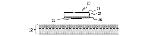
- FIG. 10 is a diagram illustrating a configuration of a sheet transmission system according to the fifth embodiment.
- the sheet transmission system according to the first embodiment of the invention is different in that the dielectric 35 is integrated with the proximity coupler 20.
- Other configurations are the same as those of the first embodiment.
- the dielectric 35 is a sheet-like dielectric layer having the same shape as the dielectric 21 of the proximity coupler 20 in plan view.
- the dielectric 35 abuts on the outer surface (lower surface) of the dielectric 21 of the proximity coupler 20.
- a patch conductor 23 is provided on the lower surface of the dielectric 35 (the surface opposite to the dielectric 21). That is, the dielectric 35 is disposed between the dielectric 21 and the patch conductor 23.
- the dielectric 35 has a higher dielectric constant than the protective layer 14 of the electromagnetic wave propagation sheet 10.
- the dielectric 35 may not be a single layer but a plurality of layers.
- the proximity coupler can be miniaturized by increasing the wavelength shortening effect.
- This structure can be realized by a laminated substrate.
- the dielectric 35 may be attached to the dielectric 21 with an adhesive and the patch conductor 23 made of a copper plate or the like may be attached thereon.
- a dielectric 35 having a dielectric constant higher than that of the protective layer 14 of the electromagnetic wave propagation sheet 10 is installed between the electromagnetic wave propagation sheet 10 and the plane-shaped conductor 22 of the proximity coupler 20. Therefore, the resonance frequency can be lowered, and the proximity coupler 20 can be reduced in size.
- the dielectric 34 is configured integrally with the proximity coupler 20, it is easy to handle and can reliably cover the entire lower surface of the proximity coupler 20. The resonance frequency can be lowered uniformly and accurately over the entire surface of the coupler 20.
- the proximity coupler 20 can be incorporated in a portable device such as a cellular phone, a portable terminal, and a portable computer.
- a portable device such as a cellular phone, a portable terminal, and a portable computer.
- the proximity coupler 20 according to the present embodiment can be reduced in size, the mobile device can be easily reduced in size and weight.
- Electromagnetic wave propagation sheet 11 Communication layer 12 Plain shaped conductor 13 Mesh shaped conductor 14 Protective layer 20
- Plain shaped conductor 23 Patch conductor 24 Slots 30 to 35 Dielectric
Landscapes
- Engineering & Computer Science (AREA)
- Computer Networks & Wireless Communication (AREA)
- Signal Processing (AREA)
- Near-Field Transmission Systems (AREA)
Description
本発明は、電磁波の伝送を行うシート伝送システム、電磁波伝播シート及び近接カプラに関する。
シート状媒体を介して電子機器の間で通信を行うシステムとして、二次元通信システムが提案されている。二次元通信システムは、電磁波伝播シートと近接カプラから構成される。近接カプラは、電磁波伝播シートの表面から染み出す電磁界を利用してシート内部との間で電磁波の入出力を行う電磁結合デバイスである。この近接カプラを電子機器のアンテナ端子と接続してシート上に設置することによってシートの任意の位置において電子機器間の通信を実現できる。このような二次元通信システムは、電磁波伝播シートの表面上で通信が可能になることから、サーフェイス通信システムと呼ばれることもある。
電磁波伝播シートと近接カプラから構成される二次元通信システムは、特許文献1や非特許文献1、非特許文献2などに開示されている。
図11に電磁波伝播シートの上に近接カプラを載せた状態の断面図を示す。電磁波伝播シート10は、誘電体(通信層)11の両面に導体2層(メッシュ形状導体13とプレーン形状導体12)を配置している。
メッシュ形状導体13の上には、メッシュ形状導体13を保護する誘電体(保護層)14が設置されている。電磁波伝播シート10内部、即ちメッシュ形状導体13とプレーン形状導体12の間を伝播する電磁波は、メッシュ形状導体13の開口部から染み出す。この二次元通信システムでは、この染み出した電磁波を介してシート上に置かれた電子機器間で通信を実現する。
この技術は、通信のみならず、電力伝送にも応用可能である。電力伝送に応用した場合には、高周波電源に接続された給電用のカプラからシート内に高周波の交流電力を注入する。そして、受電用の近接カプラは、シート表面から染み出した電磁波を吸上げて、整流回路で直流に変換し、電子機器に電力を供給する。
篠田裕之ら、「表面マイクロ波を用いた信号と電力の同時伝送法(ユビキタス・センサネットワークを支える理論、および一般)」、社団法人電子情報通信学会技術研究報告 Vol.107, No.53(20070517) pp. 115-118
A. Noda, H Shinoda, "Selective Wireless Power Transmission Through High-Q Flat Waveguide-Ring Resonator on 2-D Waveguide Sheet," IEEE Transactions on Microwave Theory and Techniques., vol.59, no.8, pp.2158-2167, Aug. 2011.
非特許文献2に開示されている電力伝送用のシステムでは、電磁波伝播シートは、保護層の誘電率が小さく、近接カプラの誘電体も保護層と同じ誘電体が使われている。そのため誘電率の高い材料を使う場合と比べて波長短縮効果が大きく得られず、近接カプラのサイズが大きくなる。例えば、このような近接カプラは、携帯端末の内蔵用としては適さない。
本発明は、このような課題を解決するためになされたものであり、近接カプラを小型化できるシート伝送システム、電磁波伝播シート及び近接カプラを提供することを目的とする。
本願発明の一態様にかかるシート伝送システムは、誘電体からなる保護層を有する電磁波伝播シートと、当該電磁波伝播シートとの間で電磁波の伝送を行う近接カプラと、前記電磁波伝播シートと、前記近接カプラにおいて給電点を有する導体との間に設けられ、前記保護層よりも誘電率が大きい第1の誘電体を備えたものである。
本願発明の一態様にかかる電磁波伝播シートは、誘電体からなる保護層を有し、近接カプラとの間で電磁波の伝送を行う電磁波伝播シートであって、近接カプラ側の最上層に、前記保護層よりも誘電率が大きい第1の誘電体層を設けたものである。
本願発明の一態様にかかる近接カプラは、スロットが設けられたプレーン形状導体と、プレーン形状導体と誘電体を介して設けられたパッチ導体とを有し、当該電磁波伝播シートとの間で電磁波の伝送を行う近接カプラであって、前記誘電体と前記パッチ導体の間に、前記誘電体よりも誘電率が高い第1の誘電体を設けたものである。
本発明によれば、近接カプラを小型化できるシート伝送システム、電磁波伝播シート及び近接カプラを提供することができる。
発明の実施の形態1.
本発明の実施の形態にかかるシート伝送システムは、電磁波伝播シートと、近接カプラにおいて給電点を有する導体との間(典型的には、電磁波伝播シートと近接カプラの間)に、電磁波伝播シートの保護層より誘電率の大きい誘電体を設置する。本実施の形態にかかるシート伝送システムでは、誘電体が電磁波伝播シートと、近接カプラにおいて給電点を有する導体との間(電磁波伝播シートと近接カプラの間)に設置されることによって、近接カプラの共振周波数を決める、プレーン形状導体と電磁波伝播シートのメッシュ形状導体の間の構造の実効誘電率が大きくなるため、近接カプラの共振周波数が低周波側にシフトする。これにより、近接カプラのサイズを小さくすることが可能となる。
本発明の実施の形態にかかるシート伝送システムは、電磁波伝播シートと、近接カプラにおいて給電点を有する導体との間(典型的には、電磁波伝播シートと近接カプラの間)に、電磁波伝播シートの保護層より誘電率の大きい誘電体を設置する。本実施の形態にかかるシート伝送システムでは、誘電体が電磁波伝播シートと、近接カプラにおいて給電点を有する導体との間(電磁波伝播シートと近接カプラの間)に設置されることによって、近接カプラの共振周波数を決める、プレーン形状導体と電磁波伝播シートのメッシュ形状導体の間の構造の実効誘電率が大きくなるため、近接カプラの共振周波数が低周波側にシフトする。これにより、近接カプラのサイズを小さくすることが可能となる。
図1は、本実施の形態1にかかるシート伝送システムの構成を示している。図1に示されるように、シート伝送システムは、電磁波伝播シート10、近接カプラ20及び誘電体30を備えている。誘電体30は、電磁波伝播シート10と、近接カプラ20の間に設けられる。
電磁波伝播シート10は、平面視が矩形の板状シートである。この電磁波伝播シート10は、剛性を有していてもよく、あるいは、折り曲げ可能であってもよい。電磁波伝播シート10は、通信層11、プレーン形状導体12、メッシュ形状導体13及び保護層14を有する。通信層11、プレーン形状導体12、メッシュ形状導体13及び保護層14はいずれもシート状である。ここで、「シート状」とは、面としての2次元の広がりを持ち、厚さが薄いものの状態を言う。シート状の一例としては、布状、紙状、箔状、板状、膜状、フィルム状、メッシュ状、などがある。
図2に電磁波伝播シート10の平面分解図を示す。通信層11は、誘電体より構成されている。この通信層11は、プレーン形状導体12とメッシュ形状導体13により挟まれている。通信層11は、電磁波伝播シート10の使用目的等に応じて材質が選択される。例えば、通信層11としては、樹脂、ゴム、ポリマーの発泡体、ゲル材等を用いることができる。
プレーン形状導体12は、通信層11の下面全体に亘って一様に拡がって設けられた表面導体層である。プレーン形状導体12は、例えば、銅やアルミニウム等の金属箔や金属板により構成される。
メッシュ形状導体13は、例えば、正方形のメッシュ形状の構造を有する裏面導体層である。メッシュの繰り返し単位は、横に隣り合う正方形の中心同士の距離に等しい。メッシュの繰返しの単位寸法は、通信層11の電磁波長より十分に短い。
なお、「メッシュ形状」とは、規則的な網目である状態の他、規則的又は不規則的な形状の複数の開口が形成されている状態を言う。メッシュ形状としては、開口部の形状が矩形である格子パターンが典型的ではあるが、その他、開口部の形状としては亀甲形、菱形、円形、三角形など各種形状をとり得る。メッシュ形状導体13は、金属(例えばアルミニウム)の薄板をエッチングすることによって製造でき、製造時にメッシュ状の部分をパターン形成してしまえばよい。
メッシュ形状導体13よりエバネッセント波と呼ばれる電磁波が滲み出すことで、メッシュ形状導体13の上方に電磁波の浸出領域が形成される。
プレーン形状導体12及びメッシュ形状導体13は、略平行な状態で配置され、プレーン形状導体12及びメッシュ形状導体13に挟まれる狭間領域を電磁波が進行する。ここでは、シート状の通信層11の両面にそれぞれプレーン形状導体12とメッシュ形状導体13とが形成されるため、通信層11内を電磁波が進行する。
保護層14は、メッシュ形状導体13の上面(通信層11と反対側の面)の全体を覆うように設けられた誘電体である。保護層14は、メッシュ形状導体13が外力によって損傷するのを防止するために設けられる。保護層14としては、例えば、樹脂、ゴム、ポリマーの発泡体、ゲル材、中空の構造体等を用いることができる。
一般的に、電磁波伝播シート10に電磁波を送り込む装置が当該電磁波伝播シート10の長手方向端部に取り付けられることで、電磁波伝播シート10上に載置される近接カプラ20との通信や給電が行われる。電磁波を送り込む装置は電磁波伝播シート10上に載置されてもよい。
近接カプラ20は、誘電体21と、その両面に設けられた2層の導体層(プレーン形状導体22、パッチ導体23)を備えるカプラ型受電装置である。近接カプラ20は、電磁波伝播シート10に載置して使用されるインタフェース装置であり、電磁波伝播シート10との間で電磁波の送受を行う。
図3に近接カプラ20の平面分解図を示す。
誘電体21としては、例えば、樹脂、ゴム、ポリマーの発泡体、ゲル材等を用いることができる。近接カプラ20の誘電体21は、電磁波伝播シート10の保護層14と同じ材料によって構成してもよい。この場合に、誘電体21と保護層14の誘電率は同じとなる。
誘電体21としては、例えば、樹脂、ゴム、ポリマーの発泡体、ゲル材等を用いることができる。近接カプラ20の誘電体21は、電磁波伝播シート10の保護層14と同じ材料によって構成してもよい。この場合に、誘電体21と保護層14の誘電率は同じとなる。
プレーン形状導体22は、給電点を有し、誘電体21の上面の全体を覆うような平面形状を有する。また、プレーン形状導体22は、その一部を細長の矩形状に切り欠いたスロット24を有する。図3に示されるように、プレーン形状導体25のスロット24の位置は、パッチ導体の内側にあり、給電点でインピーダンスマッチングがとれる位置形状をしている。給電点はスロットの両端の導体の部分に置かれる。プレーン形状導体22は、例えば、銅やアルミニウム等の金属箔や金属板により構成される。
パッチ導体23は、誘電体21の下面においてその中央近傍の一部領域を覆うような平面形状を有する。ここで、「パッチ」とは、小片、もしくは断片と言う意味であり、板状のマイクロストリップアンテナが「パッチアンテナ」と呼ばれているように、電磁波工学の分野では上述の意味で一般的に使用される用語である。パッチ導体23の長手方向の長さは、電磁波伝播シート10に当該近接カプラ20を載せたときに、電磁波伝播シート10を伝播する電磁波の周波数で共振するように設定される。パッチ導体23は、例えば、銅やアルミニウム等の金属箔や金属板により構成される。
図3に示される構成は、例えば、プリント基板によって実現できる。具体的には、プリント基板の上面にプレーン形状導体22を設け、プリント基板の下面にパッチ導体23を設ける。また、プレーン形状導体22としてはプリント基板の導体層を用い、パッチ導体23をプリント基板とは別の銅板を用いて、それらを誘電体の両面に接着して実現することも可能である。
図4及び図5に、近接カプラの他の構成例を示す。この構成例では、プレーン形状導体22に形成されている独立した電位の給電点と、パッチ導体23の間が導体25によって電気的に接続されている。導体25の位置は、給電点でインピーダンスマッチングがとれる位置に設定される。
パッチ導体23の長さは、電磁波伝播シート10に近接カプラ20を載せたときに、電磁波伝播シート10を伝播する電磁波の周波数で共振するように設定される。図4及び図5に示される構成は、例えば、プリント基板で実現される。
なお、近接カプラ20は、平板状であるが、折り曲げ可能な構成としても良い。
なお、近接カプラ20は、平板状であるが、折り曲げ可能な構成としても良い。
本実施の形態では、図1に示されるように、電磁波伝播シート10と近接カプラ20の間に、電磁波伝播シート10の保護層14よりも誘電率の高い誘電体30を設置している。誘電体30は、平板である必要はなく、波打った形でも凸凹形状でも良い。また、誘電体30は、一部に穴があいていても良い。
電磁波伝播シート10と近接カプラ20の間に保護層14と同じ誘電率の誘電体を設置しても波長短縮は大きくならない。これに対して、その位置に、保護層14よりも誘電率の高い誘電体30を設置すると、近接カプラ20のプレーン形状導体22と、電磁波伝播シート10のメッシュ形状導体13の間の構造の実効誘電率が大きくなる。このため、近接カプラ20の共振周波数が低周波側にシフトする。
特に、非特許文献2に開示されている電力伝送用のシステムのように、電磁波伝播シートの保護層の誘電率が小さく設定されている場合は、波長短縮の効果が大きい。近接カプラ20の共振周波数が低周波側にシフトすることにより、関連技術で示されるように誘電体がない場合と比較して、パッチ導体23のサイズを小さくすることができ、近接カプラ20の小型化が可能となる。そのため、関連技術に開示されたシート伝送システムと比べて、携帯端末に内蔵するのに適した近接カプラ20が実現できる。
誘電体30はパッチ導体23よりサイズが大きいことが望ましい。その理由は、パッチ導体23と電磁波伝播シート10のメッシュ形状導体13の間の電界はパッチ導体23のサイズよりも大きい範囲に広がるため、パッチ導体23のサイズよりも大きくしたほうが実効誘電率は大きくなるためである。
図6に、本実施の形態にかかるシート伝送システムが奏する効果を確認するために行った実測結果を示す。図6の下段のように、電磁波伝播シート10と近接カプラ20の間に誘電体30を設置している。メッシュ形状導体13とプレーン形状導体12の間に給電点(Port1)を設けた。また、近接カプラ20のプレーン形状導体22のスロット24の両サイドに給電点(Port2)を設けた。スロット24は、紙面垂直方向に長い形状である。そして、各給電点をネットワークアナライザに接続して伝送特性S21を測定した。電磁波伝播シートは定在波が立たないようにしてある。
近接カプラ20の誘電体21と電磁波伝播シート10の保護層14は、比誘電率1.17で厚み4mmである。これに対して、誘電体30の比誘電率は2.6で誘電正接(tanδ)は0.003である。また、メッシュ形状導体13とプレーン形状導体12の間の誘電体(通信層)11の比誘電率は2.1で厚み1mmである。
誘電体30の厚みtを変えて伝送特性を測定した結果が、図6の上段に示すグラフである。誘電体30を設置しない場合と比較して、設置することにより共振周波数(伝送量がピークを示す周波数)が低周波側にシフトしていることがわかる。さらに、誘電体30の厚みtを0.2mmから0.3mm、0.5mm、1.0mmと段階的に大きくすることにより、徐々に共振周波数が低周波側にシフトしていることがわかる。
この実測の結果から、本発明の実施の形態にかかるシート伝送システムのように、近接カプラ20と電磁波伝播シート10の間に、保護層14より誘電率の高い誘電体30を設置することにより、共振周波数が低下していることが確認できた。
発明の実施の形態2.
図7は、本実施の形態2にかかるシート伝送システムの構成を示した図である。発明の実施の形態1にかかるシート伝送システムとは、誘電体30が、単一層でなく、誘電率の異なる誘電体31と誘電体32が複数層に積層された構造を有している点で異なる。その他の構成については、発明の実施の形態1と同じである。
図7は、本実施の形態2にかかるシート伝送システムの構成を示した図である。発明の実施の形態1にかかるシート伝送システムとは、誘電体30が、単一層でなく、誘電率の異なる誘電体31と誘電体32が複数層に積層された構造を有している点で異なる。その他の構成については、発明の実施の形態1と同じである。
誘電体31と誘電体32はいずれもシート状の誘電体層である。誘電体31と誘電体32の誘電率は、誘電体31の方が誘電体32よりも大きくても、またその逆であってもよい。誘電体31と誘電体32の誘電率は、いずれも電磁波伝播シート10の保護層14よりも高い。さらに、誘電体30は、誘電体31・誘電体32の2層である必要もなく、3層以上の多層構造であっても良い。
本実施の形態2にかかるシート伝送システムにおいても、電磁波伝播シート10と近接カプラ20の間に、電磁波伝播シート10の保護層14よりも誘電率の高い誘電体31、32を設置しているため、共振周波数を低下させることができ、近接カプラ20を小型化させることが可能となる。
発明の実施の形態3.
図8は、本実施の形態3にかかるシート伝送システムの構成を示した図である。発明の実施の形態1にかかるシート伝送システムとは、誘電体33が、近接カプラ20が内蔵される電子機器の筐体を構成している点で異なる。その他の構成については、発明の実施の形態1と同じである。
図8は、本実施の形態3にかかるシート伝送システムの構成を示した図である。発明の実施の形態1にかかるシート伝送システムとは、誘電体33が、近接カプラ20が内蔵される電子機器の筐体を構成している点で異なる。その他の構成については、発明の実施の形態1と同じである。
誘電体33は、電磁波伝播シート10の保護層14よりも高い誘電率を有する。図8に示す誘電体33は、電子機器の筐体として、近接カプラ20を含む電子部品の全体を内蔵する箱体である。この例においては、筐体の全てを同じ材料からなる誘電体33により一体的に構成しているが、電磁波伝播シート10と近接カプラ20の間に位置する、筐体の一部のみを電磁波伝播シート10の保護層14よりも高い誘電率を有する誘電体33とするようにしてもよい。さらには、誘電体33は、単一層でなくとも複数層であってもよい。
本実施の形態3にかかるシート伝送システムにおいても、電磁波伝播シート10と近接カプラ20の間に、電磁波伝播シート10の保護層14よりも誘電率の高い誘電体33を設置しているため、共振周波数を低下させることができ、近接カプラ20を小型化させることが可能となる。特に、本実施の形態3では、誘電体33は近接カプラ20が内蔵される電子機器の筐体を構成しているため、筐体以外に誘電体を設ける場合に比べて、電子機器自体を小型化することができ、また部品点数を減らすことも可能となる。
発明の実施の形態4.
図9は、本実施の形態4にかかるシート伝送システムの構成を示した図である。発明の実施の形態1にかかるシート伝送システムとは、誘電体34を電磁波伝播シート10と一体にした点で異なる。その他の構成については、発明の実施の形態1と同じである。
図9は、本実施の形態4にかかるシート伝送システムの構成を示した図である。発明の実施の形態1にかかるシート伝送システムとは、誘電体34を電磁波伝播シート10と一体にした点で異なる。その他の構成については、発明の実施の形態1と同じである。
誘電体34は、電磁波伝播シート10と平面形状において同じ形状を有するシート状の誘電体層である。当該誘電体34は、電磁波伝播シート10の保護層14の外側の面(上面)で当接し、近接カプラ20側の最上層に位置する。誘電体34は、電磁波伝播シート10の保護層14よりも高い誘電率を有する。誘電体34は、単一層でなくとも複数層であってもよい。
本実施の形態4にかかるシート伝送システムにおいても、電磁波伝播シート10と近接カプラ20の間に、電磁波伝播シート10の保護層14よりも誘電率の高い誘電体34を設置しているため、共振周波数を低下させることができ、近接カプラ20を小型化させることが可能となる。特に、本実施の形態4では、誘電体34は電磁波伝播シート10と一体に構成されているため、取り扱いが容易であり、かつ電磁波伝播シート10の上面全体を確実に覆うことが可能となるため、電磁波伝播シート10の全面に亘って均一に精度良く共振周波数を低下させることができる。
発明の実施の形態5.
図10は、本実施の形態5にかかるシート伝送システムの構成を示した図である。発明の実施の形態1にかかるシート伝送システムとは、誘電体35を近接カプラ20と一体にした点で異なる。その他の構成については、発明の実施の形態1と同じである。
図10は、本実施の形態5にかかるシート伝送システムの構成を示した図である。発明の実施の形態1にかかるシート伝送システムとは、誘電体35を近接カプラ20と一体にした点で異なる。その他の構成については、発明の実施の形態1と同じである。
誘電体35は、近接カプラ20の誘電体21と平面形状において同じ形状を有するシート状の誘電体層である。当該誘電体35は、近接カプラ20の誘電体21の外側の面(下面)で当接している。この誘電体35の下面(誘電体21とは反対側の面)には、パッチ導体23が設けられている。即ち、この誘電体35は、誘電体21とパッチ導体23との間に設置されている。誘電体35は、電磁波伝播シート10の保護層14よりも高い誘電率を有する。誘電体35は、単一層でなくとも複数層であってもよい。
誘電体21が誘電体35より誘電率が低い場合、即ち、誘電体35が誘電体21よりも誘電率が高い場合、波長短縮効果が大きくなることによる近接カプラの小型化が可能である。この構造は積層基板により実現できる。また、誘電体21に誘電体35を接着材などで貼り付けてその上に銅の板等で作成されたパッチ導体23を貼り付けても良い。
本実施の形態5にかかるシート伝送システムにおいても、電磁波伝播シート10と、近接カプラ20のプレーン形状導体22の間に、電磁波伝播シート10の保護層14よりも誘電率の高い誘電体35を設置しているため、共振周波数を低下させることができ、近接カプラ20を小型化させることが可能となる。特に、本実施の形態5では、誘電体34は近接カプラ20と一体に構成されているため、取り扱いが容易であり、かつ近接カプラ20の下面全体を確実に覆うことが可能となるため、近接カプラ20の全面に亘って均一に精度良く共振周波数を低下させることができる。
その他の実施の形態.
近接カプラ20は、例えば、携帯電話、携帯端末、携帯型コンピュータ等の携帯デバイスに内蔵することができる。特に、本実施の形態にかかる近接カプラ20は、小型化が可能であるため、携帯デバイスの小型化、軽量化を容易に実現可能である。
以上、実施の形態を参照して本願発明を説明したが、本願発明は上記によって限定されるものではない。本願発明の構成や詳細には、発明のスコープ内で当業者が理解し得る様々な変更をすることができる。
近接カプラ20は、例えば、携帯電話、携帯端末、携帯型コンピュータ等の携帯デバイスに内蔵することができる。特に、本実施の形態にかかる近接カプラ20は、小型化が可能であるため、携帯デバイスの小型化、軽量化を容易に実現可能である。
以上、実施の形態を参照して本願発明を説明したが、本願発明は上記によって限定されるものではない。本願発明の構成や詳細には、発明のスコープ内で当業者が理解し得る様々な変更をすることができる。
この出願は、2012年9月24日に出願された日本出願特願2012-209910を基礎とする優先権を主張し、その開示の全てをここに取り込む。
10 電磁波伝播シート
11 通信層
12 プレーン形状導体
13 メッシュ形状導体
14 保護層
20 近接カプラ
21 誘電体
22 プレーン形状導体
23 パッチ導体
24 スロット
30~35 誘電体
11 通信層
12 プレーン形状導体
13 メッシュ形状導体
14 保護層
20 近接カプラ
21 誘電体
22 プレーン形状導体
23 パッチ導体
24 スロット
30~35 誘電体
Claims (10)
- 誘電体からなる保護層を有する電磁波伝播シートと、
当該電磁波伝播シートとの間で電磁波の伝送を行う近接カプラと、
前記電磁波伝播シートと、前記近接カプラにおいて給電点を有する導体との間に設けられ、前記保護層よりも誘電率が大きい第1の誘電体を備えたシート伝送システム。 - 前記第1の誘電体は、前記電磁波伝播シートと近接カプラの間に設けられたことを特徴とする請求項1記載のシート伝送システム。
- 前記第1の誘電体は、前記近接カプラを内蔵する電子機器の筐体であることを特徴とする請求項2記載のシート伝送システム。
- 前記第1の誘電体は、前記電磁波伝播シートの保護層よりも外側の最上層に設けられていることを特徴とする請求項2記載のシート伝送システム。
- 前記第1の誘電体は、前記近接カプラにおいて給電点を有する導体とパッチ導体の間に設けられていることを特徴とする請求項1記載のシート伝送システム。
- 前記第1の誘電体は、誘電率の異なる材料が積層された複数層より構成されていることを特徴とする請求項1~5いずれかに記載のシート伝送システム。
- 前記電磁波伝播シートは、プレーン形状導体と、メッシュ形状導体と、当該プレーン形状導体とメッシュ形状導体が両面に設けられた通信層とを有し、前記保護層は、前記メッシュ形状導体を覆う位置に設けられた請求項1から6いずれかに記載のシート伝送システム。
- 前記電磁波伝播シートの保護層と、前記近接カプラの誘電体とは、同じ誘電率を有する請求項1~7いずれかに記載のシート伝送システム。
- 誘電体からなる保護層を有し、近接カプラとの間で電磁波の伝送を行う電磁波伝播シートであって、
近接カプラ側の最上層に、前記保護層よりも誘電率が大きい第1の誘電体層を設けた電磁波伝播シート。 - スロットが設けられたプレーン形状導体と、プレーン形状導体と誘電体を介して設けられたパッチ導体とを有し、当該電磁波伝播シートとの間で電磁波の伝送を行う近接カプラであって、
前記誘電体と前記パッチ導体の間に、前記誘電体よりも誘電率が高い第1の誘電体を設けた近接カプラ。
Priority Applications (1)
| Application Number | Priority Date | Filing Date | Title |
|---|---|---|---|
| JP2014536554A JPWO2014045486A1 (ja) | 2012-09-24 | 2013-04-15 | シート伝送システム、電磁波伝播シート及び近接カプラ |
Applications Claiming Priority (2)
| Application Number | Priority Date | Filing Date | Title |
|---|---|---|---|
| JP2012-209910 | 2012-09-24 | ||
| JP2012209910 | 2012-09-24 |
Publications (1)
| Publication Number | Publication Date |
|---|---|
| WO2014045486A1 true WO2014045486A1 (ja) | 2014-03-27 |
Family
ID=50340829
Family Applications (1)
| Application Number | Title | Priority Date | Filing Date |
|---|---|---|---|
| PCT/JP2013/002540 Ceased WO2014045486A1 (ja) | 2012-09-24 | 2013-04-15 | シート伝送システム、電磁波伝播シート及び近接カプラ |
Country Status (2)
| Country | Link |
|---|---|
| JP (1) | JPWO2014045486A1 (ja) |
| WO (1) | WO2014045486A1 (ja) |
Cited By (1)
| Publication number | Priority date | Publication date | Assignee | Title |
|---|---|---|---|---|
| JP2017021806A (ja) * | 2015-07-13 | 2017-01-26 | 帝人株式会社 | 医療品管理システム、医療品管理方法、及び、プログラム |
Citations (2)
| Publication number | Priority date | Publication date | Assignee | Title |
|---|---|---|---|---|
| JP2004077503A (ja) * | 2002-06-21 | 2004-03-11 | Abel Systems Inc | 特定波長の光を透過させる光フィルター |
| JP2010252121A (ja) * | 2009-04-16 | 2010-11-04 | Serukurosu:Kk | 電磁波インタフェース装置および通信機器 |
-
2013
- 2013-04-15 JP JP2014536554A patent/JPWO2014045486A1/ja active Pending
- 2013-04-15 WO PCT/JP2013/002540 patent/WO2014045486A1/ja not_active Ceased
Patent Citations (2)
| Publication number | Priority date | Publication date | Assignee | Title |
|---|---|---|---|---|
| JP2004077503A (ja) * | 2002-06-21 | 2004-03-11 | Abel Systems Inc | 特定波長の光を透過させる光フィルター |
| JP2010252121A (ja) * | 2009-04-16 | 2010-11-04 | Serukurosu:Kk | 電磁波インタフェース装置および通信機器 |
Non-Patent Citations (2)
| Title |
|---|
| AKIHITO NODA ET AL.: "Selective Wireless Power Transmission ThroughHigh-Q Flat Waveguide-Ring Resonatoron 2-D Waveguide Sheet", IEEE TRANSACTIONS ON MICROWAVE THEORY AND TECHNIQUES, vol. 59, no. 8, 11 August 2011 (2011-08-11), pages 2158 - 2167 * |
| YASUAKI MONNAI ET AL.: "Microwave Beam Coupler between Two-Dimensional Communication Medium and Surrounding Space Using Dielectric Grating", THE TRANSACTIONS OF THE INSTITUTE OF ELECTRONICS, INFORMATION AND COMMUNICATION ENGINEERS C, vol. J92-C, no. 12, 1 December 2009 (2009-12-01), pages 797 - 805 * |
Cited By (1)
| Publication number | Priority date | Publication date | Assignee | Title |
|---|---|---|---|---|
| JP2017021806A (ja) * | 2015-07-13 | 2017-01-26 | 帝人株式会社 | 医療品管理システム、医療品管理方法、及び、プログラム |
Also Published As
| Publication number | Publication date |
|---|---|
| JPWO2014045486A1 (ja) | 2016-08-18 |
Similar Documents
| Publication | Publication Date | Title |
|---|---|---|
| KR101270562B1 (ko) | 통신단말장치 | |
| US9761950B2 (en) | Dielectric waveguide with embedded antenna | |
| US8164535B2 (en) | Coplanar waveguide FED planar log-periodic antenna | |
| US9106205B2 (en) | Wireless SAW sensors having integrated antennas | |
| US9941933B2 (en) | Magneto-inductive waveguide | |
| JP5510547B2 (ja) | アンテナ装置及び通信端末装置 | |
| CN102484507B (zh) | 通信传输装置、通信耦合器以及阻抗调整片 | |
| WO2013166589A1 (en) | Broadband end-fire multi-layer yagi antenna | |
| TW200840133A (en) | Triplate line/waveguide converter | |
| US20130193772A1 (en) | Surface communication device | |
| US9431713B2 (en) | Circularly-polarized patch antenna | |
| TW200952253A (en) | Antenna assembly, printed wiring board and device | |
| TWM544175U (zh) | 可撓性電路板 | |
| CN103098302B (zh) | 天线装置及通信装置 | |
| US8026855B2 (en) | Radio apparatus and antenna thereof | |
| JPWO2017170394A1 (ja) | 構造体、構造体の積層構造およびアンテナ構造 | |
| JP2013201712A (ja) | アンテナ基板 | |
| JP2013201711A (ja) | アンテナ基板 | |
| WO2014045486A1 (ja) | シート伝送システム、電磁波伝播シート及び近接カプラ | |
| JP5610602B2 (ja) | アンテナ基板 | |
| KR101234301B1 (ko) | 통신단말장치 | |
| JP5302079B2 (ja) | 電磁波インタフェース装置および通信機器 | |
| JP6534911B2 (ja) | 導波管・マイクロストリップ線路変換器 | |
| JP4102778B2 (ja) | アンテナ構造および通信装置 | |
| CN103296369B (zh) | 一种谐振腔 |
Legal Events
| Date | Code | Title | Description |
|---|---|---|---|
| 121 | Ep: the epo has been informed by wipo that ep was designated in this application |
Ref document number: 13838403 Country of ref document: EP Kind code of ref document: A1 |
|
| ENP | Entry into the national phase |
Ref document number: 2014536554 Country of ref document: JP Kind code of ref document: A |
|
| NENP | Non-entry into the national phase |
Ref country code: DE |
|
| 122 | Ep: pct application non-entry in european phase |
Ref document number: 13838403 Country of ref document: EP Kind code of ref document: A1 |