WO2014045440A1 - 半導体レーザ駆動回路 - Google Patents
半導体レーザ駆動回路 Download PDFInfo
- Publication number
- WO2014045440A1 WO2014045440A1 PCT/JP2012/074400 JP2012074400W WO2014045440A1 WO 2014045440 A1 WO2014045440 A1 WO 2014045440A1 JP 2012074400 W JP2012074400 W JP 2012074400W WO 2014045440 A1 WO2014045440 A1 WO 2014045440A1
- Authority
- WO
- WIPO (PCT)
- Prior art keywords
- semiconductor laser
- transistor
- current
- differential modulation
- modulation circuits
- Prior art date
- Legal status (The legal status is an assumption and is not a legal conclusion. Google has not performed a legal analysis and makes no representation as to the accuracy of the status listed.)
- Ceased
Links
Images



Classifications
-
- H—ELECTRICITY
- H01—ELECTRIC ELEMENTS
- H01S—DEVICES USING THE PROCESS OF LIGHT AMPLIFICATION BY STIMULATED EMISSION OF RADIATION [LASER] TO AMPLIFY OR GENERATE LIGHT; DEVICES USING STIMULATED EMISSION OF ELECTROMAGNETIC RADIATION IN WAVE RANGES OTHER THAN OPTICAL
- H01S5/00—Semiconductor lasers
- H01S5/04—Processes or apparatus for excitation, e.g. pumping, e.g. by electron beams
- H01S5/042—Electrical excitation ; Circuits therefor
- H01S5/0427—Electrical excitation ; Circuits therefor for applying modulation to the laser
-
- H—ELECTRICITY
- H01—ELECTRIC ELEMENTS
- H01S—DEVICES USING THE PROCESS OF LIGHT AMPLIFICATION BY STIMULATED EMISSION OF RADIATION [LASER] TO AMPLIFY OR GENERATE LIGHT; DEVICES USING STIMULATED EMISSION OF ELECTROMAGNETIC RADIATION IN WAVE RANGES OTHER THAN OPTICAL
- H01S5/00—Semiconductor lasers
- H01S5/06—Arrangements for controlling the laser output parameters, e.g. by operating on the active medium
- H01S5/068—Stabilisation of laser output parameters
- H01S5/0683—Stabilisation of laser output parameters by monitoring the optical output parameters
- H01S5/06832—Stabilising during amplitude modulation
Definitions
- the present invention relates to a semiconductor laser driving circuit for driving a semiconductor laser at high speed.
- the laser diode driving circuit includes a first transistor and a second transistor that receive a non-inverted output and an inverted output of a buffer, respectively, between a power source connected to a collector of the second transistor and a collector of the first transistor. And a connected semiconductor laser.
- the laser diode drive circuit connects a third transistor for generating a constant current to each emitter of the first transistor and the second transistor, and supplies a stable current.
- the laser diode drive circuit inputs the differential signal from the buffer to the base of the first transistor and the base of the second transistor, and switches the current flowing through the collector and emitter of these transistors at high speed. Therefore, since the current flowing through the semiconductor laser can be controlled on / off at high speed, the semiconductor laser can be driven at high speed.
- a semiconductor laser driving circuit using a constant current circuit and a differential signal is known as a high-speed on / off modulation circuit.
- the conventional semiconductor laser driving circuit is driven at high speed, it cannot perform current amount modulation because it performs on / off modulation of a constant current.
- An object of the present invention is to provide a semiconductor laser driving circuit capable of performing current amount modulation while maintaining high-speed operation.
- a semiconductor laser driving circuit includes a semiconductor laser connected to a power source, first and second switching elements, a first main electrode of the first switching element, and the first switching element.
- a first main electrode of a second switching element is connected to both ends of the semiconductor laser, a second main electrode of the first and second switching elements is connected in common, and the first switching element or the second switching element is connected
- a plurality of differential modulation circuits to be selected and a plurality of differential modulation circuits provided corresponding to the plurality of differential modulation circuits, one end of which is connected to the second main electrode of the first and second switching elements,
- a selection signal for selecting the constant current circuit and the first switching element or the second switching element in each of the plurality of differential modulation circuits is provided in front of the plurality of differential modulation circuits.
- a current control circuit for outputting to the control electrodes of the first and second switching elements.
- the first switching element or the second switching element is selected by the selection signal for each of the plurality of differential modulation circuits, current amount modulation can be performed while maintaining high-speed operation. .
- FIG. 1 is a diagram showing a configuration of a semiconductor laser driving circuit according to Embodiment 1 of the present invention.
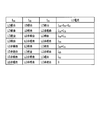
- FIG. 2 is a diagram showing the current of the semiconductor laser controlled by the control of a plurality of differential modulation circuits in the semiconductor laser driving circuit according to the first embodiment of the present invention.
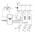
- FIG. 3 is a diagram showing a configuration of a semiconductor laser driving circuit according to Embodiment 2 of the present invention.
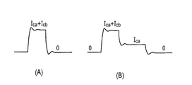
- FIG. 4 is a diagram illustrating a state in which APC is performed within one pulse in the semiconductor laser driving circuit according to the second embodiment of the present invention.
- FIG. 5 is a diagram showing a configuration of a semiconductor laser drive circuit according to Embodiment 3 of the present invention.
- FIG. 1 is a diagram showing a configuration of a semiconductor laser driving circuit according to Embodiment 1 of the present invention.
- FIG. 2 is a diagram showing the current of the semiconductor laser controlled by the control of a plurality of differential modulation circuits in the semiconductor laser driving circuit according to the first embodiment
- FIG. 6 is a diagram showing how the current is controlled so that the peak power of the semiconductor laser becomes a predetermined value in the semiconductor laser drive circuit according to the third embodiment of the present invention.
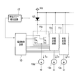
- FIG. 7 is a diagram showing a configuration of a semiconductor laser driving circuit according to Embodiment 4 of the present invention.
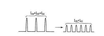
- FIG. 8 is a diagram illustrating how the current is controlled so that the average power becomes a predetermined value in the semiconductor laser driving circuit according to the fourth embodiment of the present invention.
- the semiconductor laser driving circuit includes a semiconductor laser LD, a current control circuit 10, differential modulation circuits 11a, 11b, and 11c, and constant current circuits 13a, 13b, and 13c. ing.
- the semiconductor laser LD is composed of a laser diode and is connected to a power source Vcc.
- Each of the differential modulation circuits 11a, 11b, and 11c includes a transistor Tr1 (first switching element) and a transistor Tr2 (second switching element).
- the collector (first main electrode) of the transistor Tr1 and the collector (first main electrode) of the transistor Tr2 are connected to both ends of the semiconductor laser LD, the emitter (second main electrode) of the transistor Tr1 and the emitter (second second) of the transistor Tr2. Main electrode) is connected in common.
- Each of the differential modulation circuits 11a, 11b, and 11c performs current control of the semiconductor laser LD by selecting the transistor Tr1 or the transistor Tr2 according to a selection signal from the current control circuit 10.
- Each of the constant current circuits 13a, 13b, 13c includes differential modulation circuits 11a, 11b. , 11c, one end of which is connected to the emitter of the transistor Tr1 and the emitter of the transistor Tr2, and allows constant currents Ica, Icb, Icc to flow.
- the current control circuit 10 outputs a selection signal for selecting the transistor Tr1 or the transistor Tr2 in each of the differential modulation circuits 11a, 11b, and 11c to the transistor Tr1 in each of the differential modulation circuits 11a, 11b, and 11c. Output to the base (control electrode) and the base (control electrode) of the transistor Tr2.
- the transistor Tr1 is turned on and the transistor Tr2 is turned off.
- the transistor Tr1 is turned off and the transistor Tr2 is turned on.
- a current of (Ica + Icb) flows through the semiconductor laser LD.
- the transistor Tr1 of the differential modulation circuits 11a and 11c is turned on and the transistor Tr2 is turned off.
- the transistor Tr1 is turned off and the transistor Tr2 is turned on.
- a current of (Ica + Icc) flows through the semiconductor laser LD.
- the transistor Tr1 of the differential modulation circuit 11a is turned on and the transistor Tr2 is turned off.
- the transistor Tr1 is turned off and the transistor Tr2 is turned on.
- a current of (Ica) flows through the semiconductor laser LD.
- the transistor Tr1 of the differential modulation circuits 11b and 11c is turned on and the transistor Tr2 is turned off.
- the transistor Tr1 is turned off and the transistor Tr2 is turned on.
- a current of (Icb + Icc) flows through the semiconductor laser LD.
- the transistor Tr1 of the differential modulation circuit 11b is turned on and the transistor Tr2 is turned off by the selection signal from the current control circuit 10.
- the transistor Tr1 is turned off and the transistor Tr2 is turned on.
- a current of (Icb) flows through the semiconductor laser LD.
- the transistor Tr1 of the differential modulation circuit 11c is turned on and the transistor Tr2 is turned off.
- the transistor Tr1 is turned off and the transistor Tr2 is turned on.
- a current of (Icc) flows through the semiconductor laser LD.
- the current flowing through the semiconductor laser LD can be controlled with 3-bit gradation as shown in FIG.
- the current Ica is 200 mA
- the current Icb is 100 mA
- the current Icc is Assuming 50 mA, eight types of LD currents from 0 A to a maximum of 350 mA in 50 mA increments can be selected.
- the current control circuit 10 only needs to turn on / off the transistors Tr1 and Tr2 in the differential modulation circuits 11a, 11b, and 11c, and therefore can be constituted by a digital circuit.
- the N differential modulation circuit when the constant current circuit provided N pieces is, Ica, Icb, the ratio of Icc .. Icn, 2 1, 2 2, 2 3, by taking into .. 2 n N-bit gradation current control is possible.
- the current flowing through the semiconductor laser LD can be precisely controlled by the number of the plurality of differential modulation circuits, the number of the plurality of constant current circuits, and the current value of each constant current circuit.
- the transistor Tr1 or the transistor Tr2 is selected by the selection signal, so that it is possible to perform current amount modulation while maintaining high-speed operation.
- FIG. 3 is a diagram showing a configuration of a semiconductor laser drive circuit according to the second embodiment of the present invention.
- the semiconductor laser driving circuit according to the second embodiment is characterized in that a power detection circuit 14 is further provided to the semiconductor laser driving circuit according to the first embodiment.
- the power detection circuit 14 includes a photodiode that detects the power of the semiconductor laser LD, and a current-voltage conversion circuit that converts a current flowing through the photodiode into a voltage, and outputs the converted voltage to the current control circuit 10.
- the current control circuit 10 includes the transistors Tr1 or transistors of the differential modulation circuits 11a, 11b, and 11c so that the voltage corresponding to the power of the semiconductor laser LD detected by the power detection circuit 14 becomes the value of the APC setting signal. By selecting Tr2, the current flowing through the semiconductor laser LD is controlled. In this case, the current control circuit 10 performs APC within one pulse.
- the transistors Tr1 of the differential modulation circuits 11a and 11b are turned on so that the voltage corresponding to the power of the semiconductor laser LD detected by the power detection circuit 14 becomes the APC setting signal.
- the example shown in FIG. 4B is similar to the example shown in FIG.
- the current flowing through the semiconductor laser LD can be controlled by performing the APC control within one pulse.
- FIG. 5 is a diagram showing a configuration of a semiconductor laser driving circuit according to Embodiment 3 of the present invention.
- the semiconductor laser drive circuit according to the third embodiment is characterized in that a peak power detection circuit 15 is further provided to the semiconductor laser drive circuit according to the first embodiment.
- the peak power detection circuit 15 is a photodiode that detects the power of the semiconductor laser LD, a current-voltage conversion circuit that converts the current flowing through the photodiode into a voltage, and a peak that holds the peak of the voltage converted by the current-voltage conversion circuit. A peak holding power is output to the current control circuit 10.
- the current control circuit 10 selects each transistor Tr1 or transistor Tr2 of the differential modulation circuits 11a, 11b, and 11c so that the peak power of the semiconductor laser LD detected by the peak power detection circuit 15 becomes a predetermined value. Thus, the current flowing through the semiconductor laser LD is controlled.
- the peak power of the semiconductor laser LD can be set to a predetermined value by controlling the current of (Ica + Icb) to flow through the semiconductor laser LD as in the pulse on the right side of FIG.
- FIG. 7 is a diagram showing a configuration of a semiconductor laser driving circuit according to Embodiment 4 of the present invention.
- the semiconductor laser drive circuit according to the fourth embodiment is characterized in that an average power detection circuit 17 is further provided to the semiconductor laser drive circuit according to the first embodiment.
- the average power detection circuit 17 includes a photodiode that detects the power of the semiconductor laser LD, a current-voltage conversion circuit that converts a current flowing through the photodiode into a voltage, and an average circuit that averages the voltage converted by the current-voltage conversion circuit. And outputs the averaged power to the current control circuit 10.
- the current control circuit 10 selects each transistor Tr1 or transistor Tr2 of the differential modulation circuits 11a, 11b, and 11c so that the average power of the semiconductor laser LD detected by the average power detection circuit 17 becomes a predetermined value. Thus, the current flowing through the semiconductor laser LD is controlled.
- a current of (Ica + Icb + Icc) flows through the semiconductor laser LD.
- the average power of the semiconductor laser LD can be set to a predetermined value by controlling the current (Icb + Icc) to flow through the semiconductor laser LD. it can. That is, the current control circuit 10 performs control so as to decrease the current when the frequency increases.
- the present invention is not limited to the semiconductor laser drive circuit according to the first to fourth embodiments.
- two or more semiconductor laser driving circuits according to the second to fourth embodiments may be used in combination.
- the present invention is applicable to, for example, a high-speed optical communication device.
Landscapes
- Physics & Mathematics (AREA)
- Condensed Matter Physics & Semiconductors (AREA)
- General Physics & Mathematics (AREA)
- Electromagnetism (AREA)
- Optics & Photonics (AREA)
- Semiconductor Lasers (AREA)
Description
本発明は、半導体レーザを高速駆動する半導体レーザ駆動回路に関する。
従来のこの種の半導体レーザ駆動回路として、例えば特許文献1に記載されたレーザダイオード駆動装置が知られている。このレーザダイオード駆動回路は、バッファの非反転出力及び反転出力をそれぞれベースに入力する第1トランジスタ及び第2トランジスタと、第2トランジスタのコレクタに接続された電源と第1トランジスタのコレクタとの間に接続された半導体レーザとを有する。
また、レーザダイオード駆動回路は、第1トランジスタ及び第2トランジスタの各エミッタに定電流生成用の第3トランジスタを接続し、安定した電流を供給する。
さらに、レーザダイオード駆動回路は、バッファからの差動信号を第1トランジスタのベースと第2トランジスタのベースとに入力して、これらのトランジスタのコレクタ及びエミッタに流れる電流を高速にスイッチングする。これにより、半導体レーザに流れる電流を高速にオン/オフ制御できるので、半導体レーザを高速に駆動することができる。
このように、定電流回路と差動信号とを用いた半導体レーザ駆動回路は、高速なオン/オフ変調回路として知られている。
しかしながら、従来の半導体レーザ駆動回路は、高速駆動しているが、一定電流のオン/オフ変調を行っているため、電流量変調を行うことができなかった。
本発明は、高速動作を維持したままで、電流量変調を行うことができる半導体レーザ駆動回路を提供することを目的とする。
上記の課題を解決するために、本発明に係る半導体レーザ駆動回路は、電源に接続された半導体レーザと、第1及び第2スイッチング素子を有し前記第1スイッチング素子の第1主電極と前記第2スイッチング素子の第1主電極とが前記半導体レーザの両端に接続され、前記第1及び第2スイッチング素子の第2主電極が共通接続され、前記第1スイッチング素子又は前記第2スイッチング素子を選択する複数の差動変調回路と、前記複数の差動変調回路に対応して設けられ、一端が前記第1及び第2スイッチング素子の前記第2主電極に接続され、定電流を流す複数の定電流回路と、前記複数の差動変調回路の各々の内の前記第1スイッチング素子又は前記第2スイッチング素子を選択するための選択信号を前記複数の差動変調回路の前記第1及び第2スイッチング素子の制御電極に出力する電流制御回路とを備える。
本発明によれば、複数の差動変調回路の各々について、選択信号により第1スイッチング素子又は第2スイッチング素子が選択されるので、高速動作を維持したままで、電流量変調を行うことができる。
以下、本発明のいくつかの実施例に係る半導体レーザ駆動回路が、図面を参照しながら詳細に説明される。
本発明の実施例1に係る半導体レーザ駆動回路は、図1に示すように、半導体レーザLD、電流制御回路10、差動変調回路11a,11b,11c、定電流回路13a,13b,13cを備えている。
半導体レーザLDは、レーザダイオードからなり、電源Vccに接続される。差動変調回路11a,11b,11cの各々は、トランジスタTr1(第1スイッチング素子)とトランジスタTr2(第2スイッチング素子)とを有している。
トランジスタTr1のコレクタ(第1主電極)とトランジスタTr2のコレクタ(第1主電極)とが半導体レーザLDの両端に接続され、トランジスタTr1のエミッタ(第2主電極)とトランジスタTr2のエミッタ(第2主電極)とが共通接続されている。差動変調回路11a,11b,11cの各々は、電流制御回路10からの選択信号により、トランジスタTr1又はトランジスタTr2を選択することにより、半導体レーザLDの電流制御を行う。
定電流回路13a,13b,13cの各々は、差動変調回路11a,11b.,11cに対応して設けられ、一端がトランジスタTr1のエミッタとトランジスタTr2のエミッタに接続され、定電流Ica,Icb,Iccを流す。
電流制御回路10は、差動変調回路11a,11b,11cの各々の内のトランジスタTr1又はトランジスタTr2を選択するための選択信号を差動変調回路11a,11b,11cの各々の内のトランジスタTr1のベース(制御電極)及びトランジスタTr2のベース(制御電極)に出力する。
次に、このように構成された実施例1に係る半導体レーザ駆動回路の動作を図1及び図2を参照しながら詳細に説明する。
まず、電流制御回路10からの選択信号により、差動変調回路11a,11b,11cの全てのトランジスタTr1はオンし、且つ全てのトランジスタTr2はオフする。このとき、半導体レーザLDには、(Ica+Icb+Icc)の電流が流れる。
また、電流制御回路10からの選択信号により、差動変調回路11a,11bではトランジスタTr1がオンし、トランジスタTr2がオフする。差動変調回路11cでは、トランジスタTr1がオフし、トランジスタTr2がオンする。このとき、半導体レーザLDには、(Ica+Icb)の電流が流れる。
また、電流制御回路10からの選択信号により、差動変調回路11a,11cのトランジスタTr1がオンし、トランジスタTr2がオフする。差動変調回路11bでは、トランジスタTr1がオフし、トランジスタTr2がオンする。このとき、半導体レーザLDには、(Ica+Icc)の電流が流れる。
また、電流制御回路10からの選択信号により、差動変調回路11aのトランジスタTr1がオンし、トランジスタTr2がオフする。差動変調回路11b,11cでは、トランジスタTr1がオフし、トランジスタTr2がオンする。このとき、半導体レーザLDには、(Ica)の電流が流れる。
また、電流制御回路10からの選択信号により、差動変調回路11b,11cのトランジスタTr1がオンし、トランジスタTr2がオフする。差動変調回路11aでは、トランジスタTr1がオフし、トランジスタTr2がオンする。このとき、半導体レーザLDには、(Icb+Icc)の電流が流れる。
また、電流制御回路10からの選択信号により、差動変調回路11bのトランジスタTr1がオンし、トランジスタTr2がオフする。差動変調回路11a,11cでは、トランジスタTr1がオフし、トランジスタTr2がオンする。このとき、半導体レーザLDには、(Icb)の電流が流れる。
また、電流制御回路10からの選択信号により、差動変調回路11cのトランジスタTr1がオンし、トランジスタTr2がオフする。差動変調回路11a,11bでは、トランジスタTr1がオフし、トランジスタTr2がオンする。このとき、半導体レーザLDには、(Icc)の電流が流れる。
また、電流制御回路10からの選択信号により、差動変調回路11a,11b,11cの全てのトランジスタTr1がオフし、全てのトランジスタTr2がオンすると、半導体レーザLDには電流は流れない。
このように、選択信号により全ての差動変調回路11a,11b,11cを制御することにより、半導体レーザLDに流れる電流を図2に示すように、3ビット階調で制御することができる。
例えば、図2に示すように、3つの差動変調回路11a,11b,11c、定電流回路13a,13b,13cが設けられた場合には、電流Icaを200mA、電流Icbを100mA、電流Iccを50mAとすると、0Aから50mA刻みで最大350mAまでの8種類のLD電流を選択することができる。
電流制御回路10は、差動変調回路11a,11b,11c内のトランジスタTr1,Tr2をオン/オフするだけで良いので、デジタル回路で構成することができる。
また、差動変調回路をN個設け、定電流回路をN個設けた場合には、Ica,Icb,Icc‥Icnの比を、21,22,23,‥2nにとることにより、nビット階調の電流制御が可能となる。
また、複数の差動変調回路の数、複数の定電流回路の数、各定電流回路の電流値により、半導体レーザLDに流れる電流を精密に制御することができる。
このように、複数の差動変調回路11a,11b,11cの各々について、選択信号によりトランジスタTr1又はトランジスタTr2が選択されるので、高速動作を維持したままで、電流量変調を行うことができる。
図3は本発明の実施例2に係る半導体レーザ駆動回路の構成を示す図である。実施例2に係る半導体レーザ駆動回路は、実施例1に係る半導体レーザ駆動回路に対してさらにパワー検出回路14を設けたことを特徴とする。
パワー検出回路14は、半導体レーザLDのパワーを検出するフォトダイオードと、フォトダイオードに流れる電流を電圧に変換する電流電圧変換回路とを有し、変換された電圧を電流制御回路10に出力する。
電流制御回路10は、パワー検出回路14で検出された半導体レーザLDのパワーに対応する電圧がAPC設定信号の値になるように、差動変調回路11a,11b,11cの各々のトランジスタTr1又はトランジスタTr2を選択することにより、半導体レーザLDに流れる電流を制御する。この場合、電流制御回路10は、1つのパルス内でAPCを行う。
図4(A)に示す例では、パワー検出回路14で検出された半導体レーザLDのパワーに対応する電圧がAPC設定信号になるように、差動変調回路11a,11bのトランジスタTr1をオンさせて、半導体レーザLDに(Ica+Icb)の電流が流れる。図4(B)に示す例も図4(A)に示す例と同様である。
このように実施例2に係る半導体レーザ駆動回路によれば、1つのパルス内でAPC制御を行うことにより半導体レーザLDに流れる電流を制御することができる。
図5は本発明の実施例3に係る半導体レーザ駆動回路の構成を示す図である。実施例3に係る半導体レーザ駆動回路は、実施例1に係る半導体レーザ駆動回路に対して、さらに、ピークパワー検出回路15を設けたことを特徴とする。
ピークパワー検出回路15は、半導体レーザLDのパワーを検出するフォトダイオードと、フォトダイオードに流れる電流を電圧に変換する電流電圧変換回路と、電流電圧変換回路で変換された電圧のピークをホールドするピークホールド回路とを有し、ピークホールドされたピークパワーを電流制御回路10に出力する。
電流制御回路10は、ピークパワー検出回路15で検出された半導体レーザLDのピークパワーが所定値になるように、差動変調回路11a,11b,11cの各々のトランジスタTr1又はトランジスタTr2を選択することにより、半導体レーザLDに流れる電流を制御する。
例えば、図6の左側のパルスのように、半導体レーザLDに(Ica+Icb+Icc)の電流が流れていた場合に、温度の変化によって、半導体レーザLDの発光効率が変化することがある。このような場合でも、図6の右側のパルスのように、半導体レーザLDに(Ica+Icb)の電流を流すように制御することで、半導体レーザLDのピークパワーを所定値にすることができる。
図7は本発明の実施例4に係る半導体レーザ駆動回路の構成を示す図である。実施例4に係る半導体レーザ駆動回路は、実施例1に係る半導体レーザ駆動回路に対してさらに平均パワー検出回路17を設けたことを特徴とする。
平均パワー検出回路17は、半導体レーザLDのパワーを検出するフォトダイオードと、フォトダイオードに流れる電流を電圧に変換する電流電圧変換回路と、電流電圧変換回路で変換された電圧を平均する平均回路とを有し、平均されたパワーを電流制御回路10に出力する。
電流制御回路10は、平均パワー検出回路17で検出された半導体レーザLDの平均パワーが所定値になるように、差動変調回路11a,11b,11cの各々のトランジスタTr1又はトランジスタTr2を選択することにより、半導体レーザLDに流れる電流を制御する。
例えば、図8に示すように、第1周波数を有する左側の3つのパルスの場合には、半導体レーザLDに(Ica+Icb+Icc)の電流が流れている。周波数が上昇して例えば、右側の6つのパルスになった場合には、半導体レーザLDに(Icb+Icc)の電流を流すように制御することで、半導体レーザLDの平均パワーを所定値にすることができる。即ち、電流制御回路10は、周波数が上昇した場合には、電流を低下させるように制御する。
なお、本発明は、実施例1乃至実施例4に係る半導体レーザ駆動回路に限定されるものではない。本発明は、実施例2乃至実施例4に係る半導体レーザ駆動回路の2つ以上を組み合わせて用いても良い。
本発明は、例えば、高速の光通信装置に適用可能である。
Claims (4)
- 電源に接続された半導体レーザと、
第1及び第2スイッチング素子を有し前記第1スイッチング素子の第1主電極と前記第2スイッチング素子の第1主電極とが前記半導体レーザの両端に接続され、前記第1及び第2スイッチング素子の第2主電極が共通接続され、前記第1スイッチング素子又は前記第2スイッチング素子を選択する複数の差動変調回路と、
前記複数の差動変調回路に対応して設けられ、一端が前記第1及び第2スイッチング素子の前記第2主電極に接続され、定電流を流す複数の定電流回路と、
前記複数の差動変調回路の各々の内の前記第1スイッチング素子又は前記第2スイッチング素子を選択するための選択信号を前記複数の差動変調回路の前記第1及び第2スイッチング素子の制御電極に出力する電流制御回路と、
を備える半導体レーザ駆動回路。 - 前記半導体レーザのパワーを検出するパワー検出回路を備え、
前記電流制御回路は、前記パワー検出回路で検出された前記半導体レーザのパワーが設定値になるように、前記複数の差動変調回路の各々の内の前記第1トランジスタ又は前記第2トランジスタを選択することにより、前記半導体レーザに流れる電流を制御する請求項1記載の半導体レーザ駆動回路。 - 前記半導体レーザのピークパワーを検出するピークパワー検出回路を備え、
前記電流制御回路は、前記ピークパワー検出回路で検出された前記半導体レーザのピークパワーが所定値になるように、前記複数の差動変調回路の各々の内の前記第1トランジスタ又は前記第2トランジスタを選択することにより、前記半導体レーザに流れる電流を制御する請求項1又は請求項2記載の半導体レーザ駆動回路。 - 前記半導体レーザの平均パワーを検出する平均パワー検出回路を備え、
前記電流制御回路は、前記平均パワー検出回路で検出された前記半導体レーザの平均パワーが所定値になるように、前記複数の差動変調回路の各々の内の前記第1トランジスタ又は前記第2トランジスタを選択することにより、前記半導体レーザに流れる電流を制御する請求項1乃至請求項3のいずれか1項記載の半導体レーザ駆動回路。
Priority Applications (1)
| Application Number | Priority Date | Filing Date | Title |
|---|---|---|---|
| PCT/JP2012/074400 WO2014045440A1 (ja) | 2012-09-24 | 2012-09-24 | 半導体レーザ駆動回路 |
Applications Claiming Priority (1)
| Application Number | Priority Date | Filing Date | Title |
|---|---|---|---|
| PCT/JP2012/074400 WO2014045440A1 (ja) | 2012-09-24 | 2012-09-24 | 半導体レーザ駆動回路 |
Publications (1)
| Publication Number | Publication Date |
|---|---|
| WO2014045440A1 true WO2014045440A1 (ja) | 2014-03-27 |
Family
ID=50340788
Family Applications (1)
| Application Number | Title | Priority Date | Filing Date |
|---|---|---|---|
| PCT/JP2012/074400 Ceased WO2014045440A1 (ja) | 2012-09-24 | 2012-09-24 | 半導体レーザ駆動回路 |
Country Status (1)
| Country | Link |
|---|---|
| WO (1) | WO2014045440A1 (ja) |
Cited By (1)
| Publication number | Priority date | Publication date | Assignee | Title |
|---|---|---|---|---|
| JP2016103640A (ja) * | 2014-11-28 | 2016-06-02 | 住友電気工業株式会社 | レーザ駆動回路 |
Citations (4)
| Publication number | Priority date | Publication date | Assignee | Title |
|---|---|---|---|---|
| JPS58106962U (ja) * | 1982-01-14 | 1983-07-21 | 日本電気株式会社 | レ−ザ−ダイオ−ド駆動回路 |
| JPH01206366A (ja) * | 1988-02-12 | 1989-08-18 | Ricoh Co Ltd | 半導体レーザー出力制御装置 |
| JPH0541554A (ja) * | 1991-08-06 | 1993-02-19 | Fujitsu Ltd | レーザダイオード駆動回路 |
| JP2003059083A (ja) * | 2001-08-14 | 2003-02-28 | Sony Corp | 光学ヘッドおよび光ディスク再生装置 |
-
2012
- 2012-09-24 WO PCT/JP2012/074400 patent/WO2014045440A1/ja not_active Ceased
Patent Citations (4)
| Publication number | Priority date | Publication date | Assignee | Title |
|---|---|---|---|---|
| JPS58106962U (ja) * | 1982-01-14 | 1983-07-21 | 日本電気株式会社 | レ−ザ−ダイオ−ド駆動回路 |
| JPH01206366A (ja) * | 1988-02-12 | 1989-08-18 | Ricoh Co Ltd | 半導体レーザー出力制御装置 |
| JPH0541554A (ja) * | 1991-08-06 | 1993-02-19 | Fujitsu Ltd | レーザダイオード駆動回路 |
| JP2003059083A (ja) * | 2001-08-14 | 2003-02-28 | Sony Corp | 光学ヘッドおよび光ディスク再生装置 |
Cited By (1)
| Publication number | Priority date | Publication date | Assignee | Title |
|---|---|---|---|---|
| JP2016103640A (ja) * | 2014-11-28 | 2016-06-02 | 住友電気工業株式会社 | レーザ駆動回路 |
Similar Documents
| Publication | Publication Date | Title |
|---|---|---|
| JP4566692B2 (ja) | 発光ダイオード駆動装置及びそれを備えた光伝送装置 | |
| US10511144B2 (en) | Semiconductor light-emitting device | |
| JP2015195354A (ja) | 半導体光源駆動装置、及び投写型映像表示装置 | |
| JP2014225486A (ja) | 半導体レーザー駆動装置及び画像形成装置 | |
| JP6343865B2 (ja) | 発光ダイオード点灯装置及び該発光ダイオード点灯装置を用いた照明装置 | |
| TWI440393B (zh) | 發光二極體驅動系統 | |
| JPWO2005096480A1 (ja) | 電源装置および表示装置 | |
| WO2014045440A1 (ja) | 半導体レーザ駆動回路 | |
| CN102196619A (zh) | 发光二极管的驱动电路与驱动方法 | |
| JP2010028775A (ja) | 受光アンプ回路 | |
| CN104680986A (zh) | 一种背光模组、液晶显示器及显示装置 | |
| JP2010283740A (ja) | フォトmosリレー駆動回路およびそれを用いた半導体試験装置 | |
| JP2006165545A (ja) | 発光ダイオードの高速点滅回路 | |
| JP2018022717A (ja) | 半導体発光素子駆動回路 | |
| US8101900B2 (en) | Circuit and method for operating a circuit | |
| JP2015065505A (ja) | 信号振幅検出回路 | |
| JP2015012252A (ja) | 電流検出回路 | |
| JP2006100555A (ja) | 発光素子駆動回路および前置増幅回路 | |
| JP2010067663A (ja) | リレー回路 | |
| JP2017059825A (ja) | 半導体光源駆動装置、及び投写型映像表示装置 | |
| JP2008054042A (ja) | 絶縁型接点出力回路 | |
| JP2008004701A (ja) | 発光装置及び発光素子駆動方法 | |
| JP5637886B2 (ja) | 半導体リレー | |
| JP2009159344A (ja) | 発振回路 | |
| JP4170998B2 (ja) | 温度制御装置 |
Legal Events
| Date | Code | Title | Description |
|---|---|---|---|
| 121 | Ep: the epo has been informed by wipo that ep was designated in this application |
Ref document number: 12884962 Country of ref document: EP Kind code of ref document: A1 |
|
| NENP | Non-entry into the national phase |
Ref country code: DE |
|
| 122 | Ep: pct application non-entry in european phase |
Ref document number: 12884962 Country of ref document: EP Kind code of ref document: A1 |
|
| NENP | Non-entry into the national phase |
Ref country code: JP |