WO2014038519A1 - タッチパネルコントローラ、及びこれを含む集積回路、タッチパネル装置、電子機器 - Google Patents
タッチパネルコントローラ、及びこれを含む集積回路、タッチパネル装置、電子機器 Download PDFInfo
- Publication number
- WO2014038519A1 WO2014038519A1 PCT/JP2013/073564 JP2013073564W WO2014038519A1 WO 2014038519 A1 WO2014038519 A1 WO 2014038519A1 JP 2013073564 W JP2013073564 W JP 2013073564W WO 2014038519 A1 WO2014038519 A1 WO 2014038519A1
- Authority
- WO
- WIPO (PCT)
- Prior art keywords
- touch panel
- drive
- circuit
- panel controller
- period
- Prior art date
- Legal status (The legal status is an assumption and is not a legal conclusion. Google has not performed a legal analysis and makes no representation as to the accuracy of the status listed.)
- Ceased
Links
Images







Classifications
-
- G—PHYSICS
- G06—COMPUTING OR CALCULATING; COUNTING
- G06F—ELECTRIC DIGITAL DATA PROCESSING
- G06F3/00—Input arrangements for transferring data to be processed into a form capable of being handled by the computer; Output arrangements for transferring data from processing unit to output unit, e.g. interface arrangements
- G06F3/01—Input arrangements or combined input and output arrangements for interaction between user and computer
- G06F3/03—Arrangements for converting the position or the displacement of a member into a coded form
- G06F3/041—Digitisers, e.g. for touch screens or touch pads, characterised by the transducing means
- G06F3/0416—Control or interface arrangements specially adapted for digitisers
- G06F3/04166—Details of scanning methods, e.g. sampling time, grouping of sub areas or time sharing with display driving
-
- G—PHYSICS
- G06—COMPUTING OR CALCULATING; COUNTING
- G06F—ELECTRIC DIGITAL DATA PROCESSING
- G06F3/00—Input arrangements for transferring data to be processed into a form capable of being handled by the computer; Output arrangements for transferring data from processing unit to output unit, e.g. interface arrangements
- G06F3/01—Input arrangements or combined input and output arrangements for interaction between user and computer
- G06F3/03—Arrangements for converting the position or the displacement of a member into a coded form
- G06F3/041—Digitisers, e.g. for touch screens or touch pads, characterised by the transducing means
- G06F3/044—Digitisers, e.g. for touch screens or touch pads, characterised by the transducing means by capacitive means
- G06F3/0446—Digitisers, e.g. for touch screens or touch pads, characterised by the transducing means by capacitive means using a grid-like structure of electrodes in at least two directions, e.g. using row and column electrodes
Definitions
- a drive circuit that drives M capacitances formed between a sense line and M drive lines in parallel based on N M-dimensional vectors, and is driven in parallel by the drive circuit.
- a touch panel controller comprising: an inner product operation circuit that estimates a value of the M capacitances by an inner product operation of a linear sum signal based on the charges of the M capacitances and the N M-dimensional vectors;
- the present invention relates to an integrated circuit, a touch panel device, and an electronic apparatus including the same.
- Capacitance detection circuit for detecting a distribution of capacitance values of a capacitance matrix formed between M drive lines and L sense lines as a device for detecting capacitance values distributed in a matrix
- Patent Document 1 In the capacitance detection device, when the touch panel is touched with a finger or a pen, the capacitance value of the capacitance becomes small at the touched position. By detecting the change in the capacitance value, The contact position with the touch panel by the pen is detected.
- FIG. 11 is a schematic diagram showing the configuration of the touch panel device 51 disclosed in Patent Document 1.
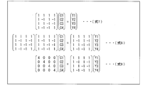
- FIG. 12 is a diagram illustrating mathematical formulas for estimating the capacity by driving the touch panel device 51 with an orthogonal code sequence.
- the touch panel device 51 includes a touch panel 52 and a touch panel controller 53.
- the touch panel 52 has drive lines DL1 to DL4, sense lines SL1 to SL4, and capacitances C11 to C44 arranged at positions where the drive lines DL1 to DL4 and sense lines SL1 to SL4 intersect. .
- the touch panel controller 53 is provided with a drive unit 54.
- the drive unit 54 drives the drive lines DL1 to DL4 based on the 4 ⁇ 4 orthogonal code sequence shown in Expression 7 of FIG.
- the element of the orthogonal code sequence is either “1” or “ ⁇ 1”. If the element is “1”, the drive unit 54 applies the voltage Vdrive, and if the element is “ ⁇ 1”, it applies ⁇ Vdrive.
- the voltage Vdrive may be a power supply voltage, but may be a voltage other than the power supply voltage.
- orthogonal code sequence is a Hadamard matrix generated by a sylvester method.
- the Hadamard matrix by the Sylvester method creates a basic unit of 2 rows x 2 columns as a basic structure.
- the upper right, upper left, and lower left bits of the basic unit are the same, and the lower right is an inversion of these bits.
- the above-mentioned 2 ⁇ 2 basic elements are synthesized as four blocks in the upper right, upper left, lower right, and lower left to create a code of a 4 ⁇ 4 bit array.
- the lower right block is bit-inverted.
- the code of the bit arrangement of 8 rows ⁇ 8 columns and 16 rows ⁇ 16 columns is generated in the same procedure.
- These matrices satisfy the above-described definition of the “orthogonal code sequence” of the present invention.
- the orthogonal code sequence of 4 rows ⁇ 4 columns shown in FIG. 12 is a Hadamard matrix of 4 rows ⁇ 4 columns by the Sylvester method.
- the Hadamard matrix refers to a square matrix whose elements are either 1 or -1 and whose rows are orthogonal to each other. That is, any two rows of the Hadamard matrix represent vectors that are perpendicular to each other.
- the “orthogonal code sequence” according to the present invention can use a matrix obtained by arbitrarily extracting N rows from an M-order Hadamard matrix (where N ⁇ M). As described below, a Hadamard matrix by a method other than the Sylvester method can also be applied to the present invention.
- Hadamard matrices obtained by methods other than these Sylvester methods can also be used as orthogonal code sequences according to the present embodiment.
- the touch panel system 51 has four amplifiers 55 arranged at positions corresponding to the sense lines SL1 to SL4, respectively.
- the amplifier 55 receives and amplifies the linear sums Y1, Y2, Y3, and Y4 along the capacitance sense line driven by the driving unit 54.
- the drive unit 54 applies the voltage Vdrive to all the drive lines DL1 to DL4. Then, for example, the measured value Y1 from the sense line SL3 expressed by the following formula 5 is output from the amplifier 55.
- the voltage Vdrive is applied to the drive lines DL1 and DL3, and ⁇ Vdrive is applied to the remaining drive lines DL2 and DL4. Then, the measured value Y2 from the sense line SL3 expressed by the following equation 6 is output from the amplifier 55.
- the voltage Vdrive is applied to the drive lines DL1 and DL2, and ⁇ Vdrive is applied to the remaining drive lines DL3 and DL4. Then, the measured value Y3 from the sense line SL3 is output from the amplifier 55. Thereafter, in the fourth drive, the voltage Vdrive is applied to the drive lines DL1 and DL4, and ⁇ Vdrive is applied to the remaining drive lines DL2 and DL3. Then, the measured value Y4 from the sense line SL3 is output from the amplifier 55.
- the capacitances C31 to C34 shown in FIG. 11 are indicated by C1 to C4 in the formulas 7 to 9 of FIG.
- the measurement values Y1 to Y4 are shown with the coefficient ( ⁇ Vdrive / Cint) omitted.
- the capacitances C1 to C4 are estimated as shown in Equation 9 by taking the inner product of the measured values Y1, Y2, Y3, Y4 and the orthogonal code sequence. Can do.
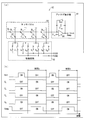
- FIG. 13A is a circuit diagram showing a configuration of another conventional touch panel device 97
- FIG. 13B is a circuit diagram for explaining the operation of the other touch panel device 97
- 14A is a diagram for explaining another operation of the other touch panel device 97
- FIG. 14B is a waveform diagram for explaining another operation of the other touch panel device 97. It is.
- the number of drive lines is 4, the number of sense lines is 1, and the drive lines DL1 and DL3 are each given a code sequence in which the given codes are all “ ⁇ 1”, and the drive lines DL2 and DL4 Is provided with a code sequence whose codes are all “1”.
- the drive line is connected to the drive voltage source VDD if the switches S1 to S4 are “ON”, and is connected (grounded) to the ground voltage GND if the switches S1 to S4 are “OFF”.
- the reference voltage Vref is given by VDD / 2.
- period a a reset period in which the analog integrator 94 is reset (a period in which the switch Rst is “ON”) will be described with reference to FIG.
- this reset period is referred to as period a.
- period b a reading period in which the output signal of the analog integrator 94 is read (a period in which the switch Rst is “OFF”) will be described with reference to FIG.
- this period is referred to as period b.
- the touch panel capacitance C11, C12, C13, C14 is increased, or the touch panel drive cycle is shortened, or the touch panel capacitance drive voltage (drive voltage in each example shown) is increased. As a result, the current consumption increases. In addition, there is a problem that current consumption increases even when the number of drive lines and the number of sense lines in the touch panel increase.
- the touch panel device described above with reference to FIGS. 13 and 14 has a problem in that power consumption increases due to an increase in touch panel capacitance, the number of sense lines, the number of drive lines, the voltage for driving the touch panel, and the drive speed of the touch panel. .
- the present invention has been made in view of the above problems, and an object thereof is to provide a touch panel controller with low power consumption, an integrated circuit including the touch panel controller, a touch panel device, and an electronic device.
- a touch panel controller parallels M capacitances formed between a sense line and M drive lines based on N M-dimensional vectors.
- a value of the M capacitances is calculated by an inner product operation of a drive circuit to be driven and a linear sum signal based on the charges of M capacitances driven in parallel by the drive circuit and the N M-dimensional vectors.
- An inner product calculation circuit for estimating wherein the drive circuit drives the capacitance so as to increase a value of a linear sum signal based on charges of the M capacitances; and the linear sum Switching between a decreasing driving state for driving to decrease the value of the signal and a sustaining driving state for driving to maintain the value of the linear sum signal based on the N M-dimensional vectors. .
- the touch panel controller reduces the value of the linear sum signal and the increased driving state in which the capacitance is driven so as to increase the value of the linear sum signal based on the charges of the M electrostatic capacitors.
- the reduced drive state that is driven in this manner and the sustain drive state that is driven so as to maintain the value of the linear sum signal are switched based on the N M-dimensional vectors.
- the drive power of the drive line can be reduced, and a touch panel controller with low power consumption can be provided.
- FIG. 1 is a circuit diagram showing a configuration of a touch panel device according to Embodiment 1.
- FIG. 2A is a diagram showing the configuration of a code sequence assigned to the drive line of the touch panel device
- FIG. 2B is a diagram showing the inner product calculation result of the code sequence. It is a wave form diagram for demonstrating operation
- 4A to 4D are circuit diagrams for explaining the operation of the touch panel device based on the waveform diagram. It is a wave form diagram for demonstrating other operation
- FIGS. 6A to 6D are circuit diagrams for explaining another operation of the touch panel device based on the waveform diagram. It is a figure for demonstrating the structure of the code series production
- FIG. 9A is a block diagram for explaining the configuration of the inner product arithmetic circuit provided in the touch panel device
- FIG. 9B is a diagram showing the configuration of a code sequence supplied to the inner product arithmetic circuit.
- . 6 is a block diagram illustrating a configuration of a mobile phone according to Embodiment 2.
- FIG. It is a circuit diagram which shows the structure of the conventional touch panel apparatus. It is a figure which shows the numerical formula for demonstrating operation
- FIG. 13A is a circuit diagram showing the configuration of another conventional touch panel device, and FIG. 13B is a circuit diagram for explaining the operation of the other touch panel device.
- FIG. 14A is a diagram for explaining another operation of the other touch panel device, and FIG. 14B is a waveform diagram for explaining another operation of the other touch panel device.
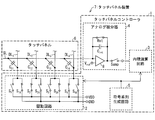
- FIG. 1 is a circuit diagram showing a configuration of touch panel device 7 according to the first embodiment.
- the touch panel device 7 includes a touch panel 6 and a touch panel controller 1 that controls the touch panel 6.
- the touch panel 6 includes a plurality of drive lines, a plurality of sense lines, and a plurality of capacitances formed in a matrix between the plurality of drive lines and the plurality of sense lines.
- FIG. 1 only four drive lines DL1 to DL4, one sense line SL, and four capacitances C11 to C14 are shown and described for the sake of simplicity.
- the touch panel controller 1 has a drive circuit 2.
- the drive circuit 2 drives in parallel four capacitances C11 to C14 formed between the sense line SL and the four drive lines DL1 to DL4 based on N M-dimensional vectors.
- FIG. 2A is a diagram showing the configuration of a code sequence assigned to the drive lines DL1 to DL4 of the touch panel device 7, and FIG. 2B is a diagram showing the inner product calculation result of the code sequence.
- the touch panel device 7 uses a code sequence having three values “1”, “ ⁇ 1”, and “0” as a code sequence to be assigned to the drive lines DL1 to DL4.
- FIG. 2A shows an example of a ternary code sequence. Here, four code sequences are shown assuming a touch panel with four drive lines.
- FIG. 3B shows the inner product calculation result of the code sequence shown in FIG. Since the inner product between the same code sequences is “8” and the inner product between different code sequences is “0”, it is possible to estimate the capacitance as in the touch panel device having the conventional configuration shown in FIG. .
- the drive circuit 2 has a switch S1 having one end connected to the drive line DL1 and the other end connected to the drive voltage source VDD, and a switch having one end connected to the drive line DL1 and the other end connected to the ground voltage source GND.
- a switch S3 having one end connected to the drive line DL3 and the other end connected to the drive voltage source VDD; a switch S3X having one end connected to the drive line DL3 and the other end connected to the ground voltage source GND; Is connected to the drive line DL4, the other end is connected to the drive voltage source VDD, and one end is the drive driver. It is connected to the down DL4, the other end and a switch S4X connected to the ground voltage source GND.
- the touch panel controller 1 is provided with an analog integrator 4.
- the analog integrator 4 reads a linear sum signal based on the electric charges of the capacitances C11 to C14 along the sense line SL.
- the analog integrator 4 has an operational amplifier 8. One input of the operational amplifier 8 is coupled to the sense line SL, and the other input is coupled to the reference voltage Vref.
- An integration capacitor Cint and a switch Rst are provided in parallel with each other between one input of the operational amplifier 8 and the output of the operational amplifier 8.
- a switch Samp is connected to the output of the operational amplifier 8.
- the touch panel controller 1 has an inner product arithmetic circuit 3.
- the inner product calculation circuit 3 estimates the values of the capacitances C11 to C14 by the inner product calculation of the linear sum signal read by the analog integrator 4 and N M-dimensional vectors.
- the drive circuit 2 is driven to increase the drive state of the capacitances C11 to C14 so as to increase the value of the linear sum signal based on the charges of the capacitances C11 to C14, and to decrease the value of the linear sum signal.
- the reduced drive state to be switched and the sustain drive state to drive so as to maintain the value of the linear sum signal are switched based on the N M-dimensional vectors.
- the drive circuit 2 connects the drive lines DL1 to DL4 to the drive voltage source VDD in the reset period in which the analog integrator 4 is reset, and the drive line in the read period in which the analog integrator 4 reads the linear sum signal.
- DL1 to DL4 are connected to the ground voltage source GDD.
- the drive circuit 2 connects the drive lines DL1 to DL4 to the ground voltage source GND in the reset period, and connects the drive lines DL1 to DL4 to the drive voltage source VDD in the read period.
- the drive circuit 2 maintains the connection state of the drive lines DL1 to DL4 before switching.
- the touch panel controller 1 is provided with a code sequence generation circuit 5.
- the code sequence generation circuit 5 generates N M-dimensional vectors based on a generation signal for generating N M-dimensional vectors and a delay generation signal obtained by delaying the generation signal.
- FIG. 3 is a waveform diagram for explaining the operation of the touch panel device 7.
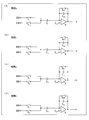
- FIGS. 4A to 4D are circuit diagrams for explaining the operation of the touch panel device 7 based on the waveform diagram.
- FIG. 5 is a waveform diagram for explaining another operation of the touch panel device 7.
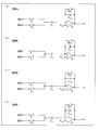
- FIGS. 6A to 6D are circuits for explaining another operation of the touch panel device 7 based on the waveform diagram.
- FIG. 3 shows an example when the value of the code sequence changes from “ ⁇ 1” to “0”.
- the switch S1 is “ON” and the switch Rst is “ON”. (Vref ⁇ VDD) ⁇ C11 Is stored.
- FIG. 5 shows an example of a waveform diagram when the value of the code sequence changes from “1” to “0”.
- the switch S1 is “OFF” and the switch Rst is “ON”.
- Vref ⁇ C11 Is stored.
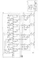
- FIG. 7 is a diagram for explaining the configuration of the code sequence generation circuit 5. The same components as those described above are given the same reference numerals. Therefore, detailed description of these components will not be repeated.
- the code sequence generation circuit 5 has a linear feedback shift register 9.
- the linear feedback shift register 9 includes shift registers 10a to 10d connected in series. A clock signal is input to each of the shift registers 10a to 10d.
- the linear feedback shift register 9 is provided with a NOR circuit 11 that receives the outputs of the shift registers 10c and 10d and supplies the output to the shift register 10a.
- the code sequence generation circuit 5 is provided with shift registers 10e to 10h connected in series to the shift register 10d. A clock signal is input to each of the shift registers 10e to 10h.
- the code sequence generation circuit 5 generates a code sequence that realizes the above-described operation and supplies it to the drive circuit 2.
- a code sequence having 15 elements is generated by the linear feedback shift register 9.
- a necessary number of code sequences are obtained by delaying the output signal of the linear feedback shift register 9 by the shift registers 10e to 10h.
- the output signal D1a of the shift register 10a and the output signal D1b of the shift register 10b are assigned to the drive line DL1
- the output signals D2a and D2b of the shift registers 10c and 10d are assigned to the drive line DL2
- the shift register The output signals D3a and D3b of 10e and 10f are assigned to the drive line DL3
- the output signals D4a and D4b of the shift registers 10g and 10h are assigned to the drive line DL4.
- the output signals D1b, D2b, D3b, and D4b are applied to the switches S1, S2, S3, and S4 of the drive lines DL1 to DL4, respectively.
- the output signals D1a, D2a, D3a, and D4a are applied to the switches S1, S2, S3, and S4 of the drive lines DL1 to DL4, respectively. If the signal applied to the switches S1, S2, S3, S4 is “1”, the drive line is connected to the drive voltage source VDD, and if it is “ ⁇ 1”, the drive line is grounded to the ground voltage source GND.
- FIG. 8 is a waveform diagram for explaining the operation of the code sequence generation circuit 5.
- the signal pattern given in FIG. 7 will be described using the example shown in FIG. Here, only the drive line DL1 is shown for simplicity.
- the drive line DL1 In the period a1, since the output signal D1b is “ ⁇ 1”, the drive line DL1 is grounded to the ground voltage source GND. Since the output signal D1a is “1” in the period b1, the drive line DL1 is connected to the drive voltage source VDD.
- the drive line DL1 is connected to the drive voltage source VDD. Since the output signal D1a is “1” in the period b2, the drive line DL1 is connected to the drive voltage source VDD.
- the operation of the switch S1 when the output signal D1a is given as a code sequence to the touch panel controller shown in FIG. 13 is shown as “S1 (conventional configuration)” in FIG.
- “S1 (conventional configuration)” shifts from “OFF” to “ON”, transition from period b1 to period a2, transition from period a3 to period b3, and transition from period a4 to period b4. And consumes power three times.
- the number of times of power consumption of the touch panel controller according to the first embodiment is one only when the period is shifted from the period a1 to the period b1. Therefore, power consumption can be reduced by using the touch panel controller according to Embodiment 1.
- FIG. 9A is a block diagram for explaining the configuration of the inner product calculation circuit 3
- FIG. 9B is a diagram showing the configuration of a code sequence supplied to the inner product calculation circuit 3.
- the analog / digital converter 12 AD-converts the linear sum signal read by the analog integrator 4 and supplies it to the inner product arithmetic circuit 3.
- the inner product calculation circuit 3 multiplies the linear sum signal supplied from the analog / digital converter 12 by the code sequence D1 corresponding to the drive line DL1 generated by the code sequence generation circuit 5, and supplies the result to the integrator I1.
- a multiplier M1 a multiplier that multiplies the code sequence D2 corresponding to the drive line DL2 generated by the code sequence generation circuit 5 and the linear sum signal supplied from the analog / digital converter 12, and supplies the multiplier I2 to the integrator I2.
- a multiplier M3 that multiplies M2, the code sequence D3 corresponding to the drive line DL3 generated by the code sequence generation circuit 5, and the linear sum signal supplied from the analog-digital converter 12 and supplies the product to the integrator I3;
- the code sequence D4 corresponding to the drive line DL4 generated by the code sequence generation circuit 5 and the analog / digital converter 12 are supplied.
- a multiplier M4 and supplies by multiplying the linear sum signal to the integrator I4 was.
- FIG. 9B shows an example of signals D1a, D1b, D2a, D2b, D3a, D3b, D4a, and D4b assigned to the drive lines DL1, DL2, DL3, and DL4.
- An analog / digital conversion is performed on the output signal of the analog integrator 4 shown in FIG. 7, and the inner product calculation circuit 3 applies the drive lines DL1 and DL2 shown in FIG. 9B to the digitally converted signal.
- DL3, and DL4 are multiplied by code sequences D1, D2, D3, and D4, respectively, and an inner product operation is performed by integrating them.
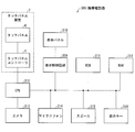
- FIG. 10 is a block diagram showing a configuration of mobile phone 300 according to Embodiment 2.
- a mobile phone 300 which is an example of an electronic device equipped with a touch panel controlled by the integrated circuit of the present invention will be described with reference to FIG.
- the cellular phone 300 includes a CPU 310, a RAM 312, a ROM 311, a camera 313, a microphone 314, a speaker 315, an operation key 316, a display panel 318, a display control circuit 309, and a touch panel device 7. .
- Each component is connected to each other by a data bus.
- CPU 310 controls the operation of mobile phone 300.
- CPU 310 executes a program stored in ROM 311, for example.
- the operation key 316 receives an instruction input from the user to the mobile phone 300.
- the RAM 312 volatilely stores data generated by execution of a program by the CPU 310 or data input through the operation keys 316.
- the ROM 311 stores data in a nonvolatile manner.
- the ROM 311 is a ROM capable of writing and erasing, such as an EPROM (Erasable Programmable Read-Only Memory) or a flash memory.
- the mobile phone 300 may include an interface (IF) for connecting to another electronic device by wire.
- IF interface
- the camera 313 captures a subject according to the operation of the operation key 316 by the user.
- the image data of the photographed subject is stored in the RAM 312 or an external memory (for example, a memory card).
- the microphone 314 receives user's voice input.
- the mobile phone 300 digitizes the input voice (analog data). Then, the mobile phone 300 sends the digitized voice to a communication partner (for example, another mobile phone).
- the speaker 315 outputs sound based on, for example, music data stored in the RAM 312.
- the touch panel device 7 includes a touch panel 6 and a touch panel controller 1 (integrated circuit).
- the CPU 310 controls the operation of the touch panel device 7.
- the CPU 310 executes a program stored in the ROM 311.
- the RAM 312 volatilely stores data generated by the CPU 310 executing the program.
- the ROM 311 stores data in a nonvolatile manner.
- the display panel 318 displays images stored in the ROM 311 and the RAM 312 by the display control circuit 309.
- the display panel 318 may be overlaid on the touch panel 302 or may incorporate the touch panel 302.
- a touch panel controller parallels M capacitances formed between a sense line and M drive lines based on N M-dimensional vectors.
- a value of the M capacitances is calculated by an inner product operation of a drive circuit to be driven and a linear sum signal based on the charges of M capacitances driven in parallel by the drive circuit and the N M-dimensional vectors.
- An inner product calculation circuit for estimating wherein the drive circuit drives the capacitance so as to increase a value of a linear sum signal based on charges of the M capacitances; and the linear sum Switching between a decreasing driving state for driving to decrease the value of the signal and a sustaining driving state for driving to maintain the value of the linear sum signal based on the N M-dimensional vectors.
- the increased driving state in which the capacitance is driven so as to increase the value of the linear sum signal based on the charges of the M capacitances, and the value of the linear sum signal is decreased.
- the electrostatic capacity is driven by switching between the decreasing driving state for driving and the sustaining driving state for driving to maintain the value of the linear sum signal based on the N M-dimensional vectors. For this reason, the frequency
- the touch panel controller further includes an analog integrator that reads the linear sum signal along the sense line, and the drive circuit is configured to reset the analog integrator in a reset period in the increased drive state.
- a drive line connected to a drive voltage source; and the analog integrator connects the drive line to a ground voltage source in a read period in which the linear sum signal is read; and in the reduced drive state, the drive line is connected in the reset period It is preferable to connect to a ground voltage source, connect the drive line to the drive voltage source in the read period, and maintain the connection state of the drive line before switching in the sustain drive state.
- the number of times of charging the capacitance can be reduced with a simple configuration.
- the drive power of the drive line can be reduced, and a touch panel controller with low power consumption can be provided.
- the N M-dimensional vectors are preferably code sequences that can take three types of values.
- a code sequence generation for generating the N M-dimensional vectors based on a generation signal for generating the N M-dimensional vectors and a delay generation signal obtained by delaying the generation signal It is preferable to further comprise a circuit.
- N M-dimensional vectors that switch between three types of driving states: an increasing driving state, a decreasing driving state, and a sustaining driving state.
- the integrated circuit according to the present invention is characterized by integrating the touch panel controller according to the present invention.
- the touch panel device includes the touch panel controller according to the present invention and a touch panel controlled by the touch panel controller.
- An electronic apparatus includes the touch panel controller according to the present invention and a touch panel controlled by the touch panel controller.
- a drive circuit that drives M capacitances formed between a sense line and M drive lines in parallel based on N M-dimensional vectors, and is driven in parallel by the drive circuit.
- a touch panel controller comprising: an inner product operation circuit that estimates a value of the M capacitances by an inner product operation of a linear sum signal based on the charges of the M capacitances and the N M-dimensional vectors; It can be used for an integrated circuit, a touch panel device, and an electronic device including this.
Landscapes
- Engineering & Computer Science (AREA)
- General Engineering & Computer Science (AREA)
- Theoretical Computer Science (AREA)
- Human Computer Interaction (AREA)
- Physics & Mathematics (AREA)
- General Physics & Mathematics (AREA)
- Position Input By Displaying (AREA)
Abstract
タッチパネルコントローラ(1)は、静電容量(C11~C14)の電荷に基づく線形和信号の値を増加させるように静電容量(C11~C14)を駆動する増加駆動状態と、線形和信号の値を減少させるように駆動する減少駆動状態と、線形和信号の値を維持させるように駆動する維持駆動状態とを、N個のM次元ベクトルに基づいて切り替える駆動回路(2)を備える。
Description
本発明は、センスラインとM本のドライブラインとの間にそれぞれ形成されたM個の静電容量をN個のM次元ベクトルに基づいて並列駆動する駆動回路と、この駆動回路により並列駆動されたM個の静電容量の電荷に基づく線形和信号と前記N個のM次元ベクトルとの内積演算により前記M個の静電容量の値を推定する内積演算回路とを備えたタッチパネルコントローラ、及びこれを含む集積回路、タッチパネル装置、電子機器に関する。
マトリックス状に分布した静電容量値を検出する装置として、M本のドライブラインとL本のセンスラインとの間に形成される静電容量行列の静電容量値の分布を検出する容量検出回路が、特許文献1に開示されている。上記容量検出装置では、指やペンでタッチパネルに触れたとき、触れられた位置において静電容量の容量値が小さくなることを利用しており、上記容量値の変化を検出することによって、指やペンによるタッチパネルとの接触位置を検出する。
(従来のタッチパネル装置)
図11は、上記特許文献1に開示されているタッチパネル装置51の構成を示す模式図である。図12は、タッチパネル装置51を直交符号系列で駆動して容量を推定するための数式を示す図である。タッチパネル装置51は、タッチパネル52とタッチパネルコントローラ53とを備えている。タッチパネル52は、ドライブラインDL1~DL4と、センスラインSL1~SL4と、ドライブラインDL1~DL4とセンスラインSL1~SL4とが交差する位置に配置された静電容量C11~C44とを有している。
図11は、上記特許文献1に開示されているタッチパネル装置51の構成を示す模式図である。図12は、タッチパネル装置51を直交符号系列で駆動して容量を推定するための数式を示す図である。タッチパネル装置51は、タッチパネル52とタッチパネルコントローラ53とを備えている。タッチパネル52は、ドライブラインDL1~DL4と、センスラインSL1~SL4と、ドライブラインDL1~DL4とセンスラインSL1~SL4とが交差する位置に配置された静電容量C11~C44とを有している。
タッチパネルコントローラ53には、駆動部54が設けられている。駆動部54は、図12の式7に示される4行4列の直交符号系列に基づいてドライブラインDL1~DL4を駆動する。直交符号系列の要素は、「1」と「-1」とのいずれかであり。要素が「1」であれば、駆動部54は電圧Vdriveを印加し、要素が「-1」であれば、-Vdriveを印加する。ここで、電圧Vdriveは、電源電圧でもよいが、電源電圧以外の電圧であってもよい。
本明細書において、「直交符号系列」とは、符号長Nの符合系列di=(di1、di2、…、diN)(i=1、…、M)が、下記に示す条件を満足することをいうものとする。

「直交符号系列」の例としては、シルベスター(sylvester)法によって生成されるアダマール(Hadamard)行列が挙げられる。
シルベスター法によるアダマール行列は、基本的な構造として、2行×2列の基本単位を作る。この基本単位の右上、左上、及び左下のビットは同一であり、右下はこれらのビット反転となっている。
次に、前述した2×2の基本要素を、右上、左上、右下、及び左下にブロックとして4つ合成して、4行×4列のビット配列の符号を作る。ここで、2×2の基本単位の作成と同様に、右下のブロックはビット反転となる。同様な手順で、8行×8列、16行×16列のビット配列の符号を生成する。これらの行列は、前述した本発明の「直交符号系列」の定義を満足する。図12に示される4行×4列の直交符号系列は、シルベスター法による4行×4列のアダマール行列である。
ここで、アダマール(Hadamard)行列とは、要素が1または-1のいずれかであり、かつ各行が互いに直交であるような正方行列をいう。すなわち、アダマール行列の任意の2つの行は、互いに垂直なベクトルを表す。
本発明に係る「直交符号系列」は、M次のアダマール行列から任意にN行取り出した行列を使用することができる(ここで、N≦Mである)。以下に述べるように、シルベスター法以外の方法によるアダマール行列も本発明に適用することができる。
シルベスター法によるN次のアダマール行列は、M=2のべき乗になるが、Mが4の倍数であれば、アダマール行列は存在するという予想が存在し、例えば、M=12のとき、及び、M=20のときにアダマール行列が存在する。これらのシルベスター法以外の方法によるアダマール行列も、本実施の形態に係る直交符号系列として使用することができる。
タッチパネルシステム51は、センスラインSL1~SL4にそれぞれ対応する位置に配置された4個の増幅器55を有している。増幅器55は、駆動部54により駆動された静電容量のセンスラインに沿った線形和Y1、Y2、Y3、Y4を受け取って増幅する。
例えば、上記4行×4列の直交符号系列による4回の駆動のうちの最初の駆動では、駆動部54はすべてのドライブラインDL1~DL4に電圧Vdriveを印加する。すると、例えば、下記の式5で示されるセンスラインSL3からの測定値Y1が増幅器55から出力される。そして、2回目の駆動では、ドライブラインDL1及びDL3に電圧Vdriveを印加し、残りのドライブラインDL2及びDL4に-Vdriveを印加する。すると、下記の式6で示されるセンスラインSL3からの測定値Y2が増幅器55から出力される。

次に、3回目の駆動では、ドライブラインDL1及びDL2に電圧Vdriveを印加し、残りのドライブラインDL3及びDL4に-Vdriveを印加する。すると、センスラインSL3からの測定値Y3が増幅器55から出力される。その後、4回目の駆動では、ドライブラインDL1及びDL4に電圧Vdriveを印加し、残りのドライブラインDL2及びDL3に-Vdriveを印加する。すると、センスラインSL3からの測定値Y4が増幅器55から出力される。
ここで、図11に示す静電容量C31~C34は、図12の式7~式9においては、説明の簡単のため、C1~C4により示している。また、図12においては、表記の簡単化のため、測定値Y1~Y4について、係数(-Vdrive/Cint)を省略して記載している。
そして、図12の式8に示すように、測定値Y1、Y2、Y3、Y4と直交符号系列との内積をとることにより、式9に示すように、静電容量C1~C4を推定することができる。
(従来の他のタッチパネル装置)
図13の(a)は従来の他のタッチパネル装置97の構成を示す回路図であり、図13の(b)は上記他のタッチパネル装置97の動作を説明するための回路図である。図14の(a)は上記他のタッチパネル装置97の他の動作を説明するための図であり、図14の(b)は上記他のタッチパネル装置97の他の動作を説明するための波形図である。
図13の(a)は従来の他のタッチパネル装置97の構成を示す回路図であり、図13の(b)は上記他のタッチパネル装置97の動作を説明するための回路図である。図14の(a)は上記他のタッチパネル装置97の他の動作を説明するための図であり、図14の(b)は上記他のタッチパネル装置97の他の動作を説明するための波形図である。
図13及び図14を用いて、特許文献1に記載されているタッチパネル装置の課題を説明する。ここでは、簡単のため、ドライブライン数を4、センスライン数を1とし、ドライブラインDL1とDL3には、与えられる符号がすべて「-1」となる符号系列が与えられ、ドライブラインDL2とDL4には符号がすべて「1」となる符号系列が与えられている。また、簡単のために、スイッチS1~S4が「ON」であれば、ドライブラインは駆動電圧源VDDに接続され、「OFF」であればグランド電圧GNDに接続される(接地される)とする。また、参照電圧VrefはVDD/2で与えられるとする。
はじめに、アナログ積分器94がリセットされているリセット期間(スイッチRstが「ON」となっている期間)、について図13を用いて説明する。以降このリセット期間を期間aとする。期間aでは、センスラインSLの電圧は、リセットされているアナログ積分器94によってVref(=VDD/2)にバイアスされている。ドライブラインDL1・DL3は接地され、ドライブラインDL2・DL4は電源に接続されていることから、静電容量C11、C12、C13、C14に蓄えられる電荷Q11a、Q12a,Q13a,Q14aは、それぞれ、
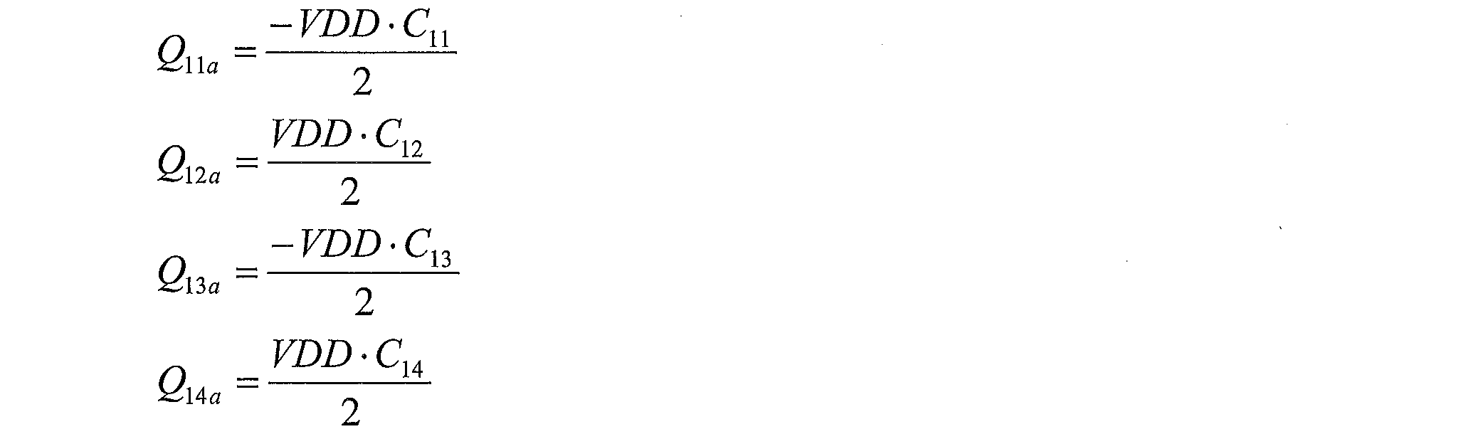
で与えられる。つぎに、アナログ積分器94の出力信号を読み出す読み出し期間(スイッチRstが「OFF」となっている期間)について図14を用いて説明する。以降この期間を期間bとする。期間bでは、アナログ積分器94のオペアンプ98のゲインが十分に大きければ、センスラインSLの電圧はVref(=VDD/2)とほぼ等しくなる。ドライブラインDL2、DL4は接地され、ドライブラインDL1、DL3は電源に接続されていることから、静電容量C11、C12、C13、C14に蓄えられる電荷Q11b、Q12b,Q13b,Q14bは、それぞれ、

で与えられる。
期間aから期間bに移行する際に、静電容量C11とC13とを充電する必要があるため、電源より、VDD・C11+VDD・C13の電荷が供給される。静電容量C12とC14の電荷はGNDに放電される。また、期間bから期間aに移行する際に、静電容量C12とC14を充電する必要があるため、電源より、VDD・C12+VDD・C14の電荷が供給される。静電容量C11とC13の電荷はGNDに放電される。すなわち、動作の1サイクル(期間aから期間bを経て期間aに至るサイクル)に掛かる時間をTとすると、1サイクルで消費される電流Icycleは、電源より供給される電荷の総量を時間Tで除算することで与えられ、

となる。タッチパネルの静電容量C11、C12、C13、C14が大きくなるか、もしくはタッチパネルを駆動する周期が短くなるか、もしくはタッチパネルの静電容量を駆動する電圧(個々の示した例では駆動電圧)が大きくなると、消費電流が増大する。また、タッチパネルのドライブライン数、センスライン数が増えても消費電流が増大するという課題がある。
図13及び図14を参照して前述したタッチパネル装置では、タッチパネル容量、センスライン数、ドライブライン数、タッチパネルを駆動する電圧、タッチパネルの駆動速度の増加によって、消費電力の増大を招くという問題がある。
本発明は、上記の問題点に鑑みてなされたものであり、その目的は、消費電力の小さいタッチパネルコントローラ、及びこれを含む集積回路、タッチパネル装置、電子機器を提供することにある。
上記の課題を解決するために、本発明に係るタッチパネルコントローラは、センスラインとM本のドライブラインとの間にそれぞれ形成されたM個の静電容量をN個のM次元ベクトルに基づいて並列駆動する駆動回路と、前記駆動回路により並列駆動されたM個の静電容量の電荷に基づく線形和信号と前記N個のM次元ベクトルとの内積演算により前記M個の静電容量の値を推定する内積演算回路とを備え、前記駆動回路は、前記M個の静電容量の電荷に基づく線形和信号の値を増加させるように前記静電容量を駆動する増加駆動状態と、前記線形和信号の値を減少させるように駆動する減少駆動状態と、前記線形和信号の値を維持させるように駆動する維持駆動状態とを、前記N個のM次元ベクトルに基づいて切り替えることを特徴とする。
本発明に係るタッチパネルコントローラは、前記M個の静電容量の電荷に基づく線形和信号の値を増加させるように前記静電容量を駆動する増加駆動状態と、前記線形和信号の値を減少させるように駆動する減少駆動状態と、前記線形和信号の値を維持させるように駆動する維持駆動状態とを、前記N個のM次元ベクトルに基づいて切り替える。その結果、ドライブラインの駆動電力を小さくすることができ、消費電力の小さいタッチパネルコントローラを提供することができる。
以下、本発明の実施の形態について、詳細に説明する。
(実施の形態1)
(タッチパネル装置7の構成)
図1は、実施の形態1に係るタッチパネル装置7の構成を示す回路図である。タッチパネル装置7は、タッチパネル6と、タッチパネル6を制御するタッチパネルコントローラ1とを備えている。タッチパネル6は、複数のドライブラインと、複数のセンスラインと、複数のドライブラインと複数のセンスラインとの間にマトリックス状に形成された複数の静電容量を有している。図1では、説明を簡素にするために、4本のドライブラインDL1~DL4、1本のセンスラインSL、4個の静電容量C11~C14のみを示して説明する。
(タッチパネル装置7の構成)
図1は、実施の形態1に係るタッチパネル装置7の構成を示す回路図である。タッチパネル装置7は、タッチパネル6と、タッチパネル6を制御するタッチパネルコントローラ1とを備えている。タッチパネル6は、複数のドライブラインと、複数のセンスラインと、複数のドライブラインと複数のセンスラインとの間にマトリックス状に形成された複数の静電容量を有している。図1では、説明を簡素にするために、4本のドライブラインDL1~DL4、1本のセンスラインSL、4個の静電容量C11~C14のみを示して説明する。
タッチパネルコントローラ1は、駆動回路2を有している。駆動回路2は、センスラインSLと4本のドライブラインDL1~DL4との間にそれぞれ形成された4個の静電容量C11~C14をN個のM次元ベクトルに基づいて並列駆動する。
図2の(a)はタッチパネル装置7のドライブライDL1~DL4に割り当てる符号系列の構成を示す図であり、図2の(b)は上記符号系列の内積演算結果を示す図である。タッチパネル装置7は、ドライブラインDL1~DL4に割り当てる符号系列として「1」、「-1」、「0」の3値を取る符号系列を用いる。図2の(a)は3値の符号系列の一例を示している。ここでは、ドライブライン数4のタッチパネルを仮定して4つの符号系列を示した。また、図3の(b)に図3の(a)に示した符号系列の内積計算結果を示す。同一の符号系列間の内積が「8」となり、異なる符号系列間の内積が「0」となることから、図11に示す従来の構成のタッチパネル装置と同様に静電容量の推定が可能である。
駆動回路2は、一端がドライブラインDL1に接続され、他端が駆動電圧源VDDに接続されたスイッチS1と、一端がドライブラインDL1に接続され、他端がグランド電圧源GNDに接続されたスイッチS1Xと、一端がドライブラインDL2に接続され、他端が駆動電圧源VDDに接続されたスイッチS2と、一端がドライブラインDL2に接続され、他端がグランド電圧源GNDに接続されたスイッチS2Xと、一端がドライブラインDL3に接続され、他端が駆動電圧源VDDに接続されたスイッチS3と、一端がドライブラインDL3に接続され、他端がグランド電圧源GNDに接続されたスイッチS3Xと、一端がドライブラインDL4に接続され、他端が駆動電圧源VDDに接続されたスイッチS4と、一端がドライブラインDL4に接続され、他端がグランド電圧源GNDに接続されたスイッチS4Xとを有している。
タッチパネルコントローラ1には、アナログ積分器4が設けられている。アナログ積分器4は、静電容量C11~C14の電荷に基づく線形和信号をセンスラインSLに沿って読み出す。
アナログ積分器4は、オペアンプ8を有している。オペアンプ8の一方の入力はセンスラインSLに結合され、他方の入力は基準電圧Vrefに結合されている。オペアンプ8の一方の入力とオペアンプ8の出力との間には、積分容量CintとスイッチRstとが互いに並行に設けられている。オペアンプ8の出力にはスイッチSampが接続されている。
タッチパネルコントローラ1は、内積演算回路3を有している。内積演算回路3は、アナログ積分器4により読み出された線形和信号とN個のM次元ベクトルとの内積演算により静電容量C11~C14の値を推定する。
駆動回路2は、静電容量C11~C14の電荷に基づく線形和信号の値を増加させるように静電容量C11~C14を駆動する増加駆動状態と、線形和信号の値を減少させるように駆動する減少駆動状態と、線形和信号の値を維持させるように駆動する維持駆動状態とを、前記N個のM次元ベクトルに基づいて切り替える。
駆動回路2は、増加駆動状態では、アナログ積分器4がリセットされるリセット期間においてドライブラインDL1~DL4を駆動電圧源VDDに接続し、アナログ積分器4が線形和信号を読み出す読み出し期間においてドライブラインDL1~DL4をグランド電圧源GDDに接続する。駆動回路2は、減少駆動状態では、リセット期間においてドライブラインDL1~DL4をグランド電圧源GNDに接続し、読み出し期間においてドライブラインDL1~DL4を駆動電圧源VDDに接続する。駆動回路2は、維持駆動状態では、切り替え前のドライブラインDL1~DL4の接続状態を維持する。
タッチパネルコントローラ1には、符号系列生成回路5が設けられている。符号系列生成回路5は、N個のM次元ベクトルを生成するための生成信号、及びこの生成信号を遅延させた遅延生成信号に基づいてN個のM次元ベクトルを生成する。
(タッチパネル装置1の動作)
実施の形態1に係るタッチパネル装置7の静電容量C11~C14の駆動方法について容量C11を例に挙げて説明する。
実施の形態1に係るタッチパネル装置7の静電容量C11~C14の駆動方法について容量C11を例に挙げて説明する。
図3はタッチパネル装置7の動作を説明するための波形図であり、図4の(a)~(d)は上記波形図に基づくタッチパネル装置7の動作を説明するための回路図である。図5はタッチパネル装置7の他の動作を説明するための波形図であり、図6の(a)~(d)は、上記波形図に基づくタッチパネル装置7の他の動作を説明するための回路図である。
図5及び図6の(a)(b)に示すように、符号系列の値が「1」であれば(減少駆動状態)、期間aでは、静電容量C11に電荷Qa11=Vref×C11が蓄えられる。期間bでは、静電容量C11に電荷Qb11=(Vref-VDD)×C11が蓄えられる。また、積分容量Cintの電荷は、Qbint=(Vref-Vout)×Cintで与えられ、
Qa11=Qb11+Qbint
となるため、
Vref×C11=(Vref-VDD)×C11 + (Vref-Vout)×Cint
であるから、
Vout=-VDD×C11/Cint + Vref
となる。
Qa11=Qb11+Qbint
となるため、
Vref×C11=(Vref-VDD)×C11 + (Vref-Vout)×Cint
であるから、
Vout=-VDD×C11/Cint + Vref
となる。
符号系列の値が「-1」であれば(増加駆動状態)、図3及び図4の(a)(b)に示すように、期間aでは、静電容量C11に電荷Qa11=(Vref-VDD)×C11が蓄えられる。期間bでは、静電容量C11に電荷Qb11=Vref×C11が蓄えられる。積分容量Cintの電荷は、Qbint=(Vref-Vout)×Cintで与えられ、
Qa11=Qb11+Qbint
となるため、
(Vref-VDD)×C11=Vref×C11 + (Vref-Vout)×Cint
であるから、
Vout=VDD×C11/Cint + Vref
となる。
Qa11=Qb11+Qbint
となるため、
(Vref-VDD)×C11=Vref×C11 + (Vref-Vout)×Cint
であるから、
Vout=VDD×C11/Cint + Vref
となる。
符号系列の値が「0」の場合は、1クロック前の符号系列の値によって1クロック前の接続状態を維持する。
図3は、符号系列の値が「-1」から「0」に変化した場合の例を示す。符号系列が「-1」の際の期間aでは、スイッチS1が「ON」であり、スイッチRstが「ON」であるため、前述のように、静電容量C11には、
(Vref-VDD)×C11
の電荷が蓄えられる。
(Vref-VDD)×C11
の電荷が蓄えられる。
符号系列が「-1」の際の期間bでは、スイッチS1が「OFF」、Rstが「OFF」であるため、前述のように、静電容量C11には、
Vref×C11
の電荷が蓄えられる。
Vref×C11
の電荷が蓄えられる。
符号系列が「0」の際の期間aでは、図3、図4の(c)に示すように、スイッチS1が「OFF」、スイッチRSTが「ON」であるため、前述のように、容量C11には、
Vref×C11
の電荷が蓄えられる。
Vref×C11
の電荷が蓄えられる。
符号系列が「0」の際の期間bでは、図3、図4の(d)に示すように、スイッチS1が「OFF」、スイッチRstが「OFF」であるため、静電容量C11には、
Vref×C11
の電荷が蓄えられる。符号系列が「-1」の際の期間aから期間bへの移行以外では電荷の移動がない。
Vref×C11
の電荷が蓄えられる。符号系列が「-1」の際の期間aから期間bへの移行以外では電荷の移動がない。
符号系列が「0」の際の期間bでは、積分容量Cintの電荷は、Qbint=(Vref-Vout)×Cintで与えられ、
Qa11=Qb11+Qbint
となるため、
Vref×C11=Vref×C11 + (Vref-Vout)×Cint
であるから、
Vout=Vref
となり、符号系列が「0」の際は、出力電圧に静電容量C11に起因する成分が含まれない。
Qa11=Qb11+Qbint
となるため、
Vref×C11=Vref×C11 + (Vref-Vout)×Cint
であるから、
Vout=Vref
となり、符号系列が「0」の際は、出力電圧に静電容量C11に起因する成分が含まれない。
次に、図5に符号系列の値が「1」から「0」へと変化した場合の波形図の例を示す。符号系列が「1」の際の期間aでは、スイッチS1が「OFF」、スイッチRstが「ON」であるため、前述のように、静電容量C11には、
Vref×C11
の電荷が蓄えられる。
Vref×C11
の電荷が蓄えられる。
符号系列が「1」の際の期間bでは、スイッチS1が「ON」、スイッチRstが「OFF」であるため、前述のように、静電容量C11には、
(Vref-VDD)×C11
の電荷が蓄えられる。
(Vref-VDD)×C11
の電荷が蓄えられる。
符号系列が「0」の際の期間aでは、スイッチS1が「ON」、スイッチRstが「ON」であるため、静電容量C11には、
(Vref-VDD)×C11
の電荷が蓄えられる。
(Vref-VDD)×C11
の電荷が蓄えられる。
符号系列が「0」の際の期間bでは、スイッチS1が「ON」、スイッチRstが「OFF」であるため、静電容量C11には、
(Vref-VDD)×C11
の電荷が蓄えられる。符号系列が「1」の際の期間aから 期間bへの移行以外では電荷の移動がない。
(Vref-VDD)×C11
の電荷が蓄えられる。符号系列が「1」の際の期間aから 期間bへの移行以外では電荷の移動がない。
符号系列が「0」の際の期間bでは、積分容量Cintの電荷は、Qbint=(Vref-Vout)×Cintで与えられ、
Qa11=Qb11+Qbint
となるため、
(Vref-VDD)×C11=(Vref-VDD)×C11 + (Vref-Vout)×Cint
であるから、
Vout=Vref
となり、符号系列が「0」の際は、出力電圧に静電容量C11に起因する成分が含まれない。
(符号系列生成回路5の具体構成)
図7は、符号系列生成回路5の構成を説明するための図である。前述した構成要素と同一の構成要素は同一の参照符号を付している。従って、これらの構成要素の詳細な説明は繰り返さない。
Qa11=Qb11+Qbint
となるため、
(Vref-VDD)×C11=(Vref-VDD)×C11 + (Vref-Vout)×Cint
であるから、
Vout=Vref
となり、符号系列が「0」の際は、出力電圧に静電容量C11に起因する成分が含まれない。
(符号系列生成回路5の具体構成)
図7は、符号系列生成回路5の構成を説明するための図である。前述した構成要素と同一の構成要素は同一の参照符号を付している。従って、これらの構成要素の詳細な説明は繰り返さない。
符号系列生成回路5は、線形帰還シフトレジスタ9を有している。線形帰還シフトレジスタ9は、直列に接続されたシフトレジスタ10a~10dを有している。各シフトレジスタ10a~10dにはクロック信号が入力される。線形帰還シフトレジスタ9には、シフトレジスタ10c・10dの出力を受け取って、出力をシフトレジスタ10aに供給するNOR回路11が設けられている。
符号系列生成回路5には、シフトレジスタ10dに直列に接続されたシフトレジスタ10e~10hが設けられている。各シフトレジスタ10e~10hにはクロック信号が入力される。
符号系列生成回路5は、前述した動作を実現する符号系列を生成して駆動回路2に供給する。線形帰還シフトレジスタ9によって、15個の要素を持つ符号系列を生成する。線形帰還シフトレジスタ9の出力信号をシフトレジスタ10e~10hによって遅延させることにより必要な数の符号系列を得る。
図7に示す例では、シフトレジスタ10aの出力信号D1aとシフトレジスタ10bの出力信号D1bとをドライブラインDL1に割り当て、シフトレジスタ10c、10dの出力信号D2a、D2bをドライブラインDL2に割り当て、シフトレジスタ10e、10fの出力信号D3a、D3bをドライブラインDL3に割り当て、シフトレジスタ10g、10hの出力信号D4a,D4bをドライブラインDL4に割り当てている。
図7に示すクロック信号が「ハイ」である期間は、各ドライブラインDL1~DL4のスイッチS1、S2、S3、S4にそれぞれ、出力信号D1b、D2b、D3b、D4bが与えられる。クロック信号が「ロー」である期間は、各ドライブラインDL1~DL4のスイッチS1、S2、S3、S4にそれぞれ、出力信号D1a、D2a、D3a、D4aが与えられる。スイッチS1、S2、S3、S4に与えられる信号が「1」であれば、そのドライブラインは駆動電圧源VDDに接続され、「-1」であればグランド電圧源GNDに接地される。
図8は、符号系列生成回路5の動作を説明するための波形図である。図7に与えられる信号パターンを図8に示す例を用いて説明する。ここでは、簡単のためドライブラインDL1についてのみ示した。期間a1では、出力信号D1bが「-1」であるため、ドライブラインDL1はグランド電圧源GNDに接地される。期間b1では出力信号D1aが「1」であるため、ドライブラインDL1は駆動電圧源VDDに接続される。期間a2では、出力信号D1bが「1」であるため、ドライブラインDL1は駆動電圧源VDDに接続される。期間b2では出力信号D1aが「1」であるため、ドライブラインDL1は駆動電圧源VDDに接続される。
期間a3では、出力信号D1bが「1」であるため、ドライブラインDL1は駆動電圧源VDDに接続される。期間b3では出力信号D1aが「-1」であるため、ドライブラインDL1はグランド電圧源GNDに接地される。期間a4では、出力信号D1bが「-1」であるため、ドライブラインDL1は接地される。期間b4では出力信号D1aが「-1」であるため、ドライブラインDL1は接地される。ドライブラインDL1が駆動電圧源VDDに接続される場合、前述のように、容量C11には、Vref=VDD/2とすると、

の電荷が蓄えられ、接地される場合

の電荷が蓄えられる。従って、電荷の移動があり、かつ駆動電圧源VDDから電荷を供給する必要があるのは、期間a1から期間b1へ移行するときのみであり、それ以外では電力を消費しない。
比較のため、図13に示すタッチパネルコントローラに、符号系列として出力信号D1aを与えた場合のスイッチS1の動作を「S1(従来構成)」として図8に示す。この場合、「S1(従来構成)」が「OFF」から「ON」に移行する、期間b1から期間a2への移行と、期間a3から期間b3への移行と、期間a4から期間b4への移行とで、3回電力を消費する。実施の形態1に係るタッチパネルコントローラの電力消費の回数は、前述したとおり、期間a1から期間b1へ移行するときのみ1回である。従って、実施の形態1に係るタッチパネルコントローラを用いることで消費電力を削減することができる。
図9の(a)は内積演算回路3の構成を説明するためのブロック図であり、図9の(b)は内積演算回路3に供給される符号系列の構成を示す図である。
アナログ・デジタル変換器12は、アナログ積分器4が読み出した線形和信号をAD変換して内積演算回路3に供給する。
内積演算回路3は、アナログ・デジタル変換器12から供給された線形和信号と、符号系列生成回路5により生成されたドライブラインDL1に対応する符号系列D1とを乗算して積分器I1に供給する乗算器M1と、符号系列生成回路5により生成されたドライブラインDL2に対応する符号系列D2とアナログ・デジタル変換器12から供給された線形和信号とを乗算して積分器I2に供給する乗算器M2と、符号系列生成回路5により生成されたドライブラインDL3に対応する符号系列D3とアナログ・デジタル変換器12から供給された線形和信号とを乗算して積分器I3に供給する乗算器M3と、符号系列生成回路5により生成されたドライブラインDL4に対応する符号系列D4とアナログ・デジタル変換器12から供給された線形和信号とを乗算して積分器I4に供給する乗算器M4とを有している。
図9の(b)は、ドライブラインDL1、DL2、DL3、DL4に割り当てる信号D1a、D1b、D2a、D2b、D3a、D3b、D4a、D4bの例を示している。
図7に示すアナログ積分器4の出力信号に対してアナログ・デジタル変換を行い、デジタル変換された信号に対して、内積演算回路3は、図9の(b)に示したドライブラインDL1、DL2、DL3、DL4にそれぞれ与えられる符号系列D1、D2、D3、D4を乗算し、それを積分することで内積演算を行う。
(実施の形態2)
(携帯電話機300の構成)
図10は、実施の形態2に係る携帯電話機300の構成を示すブロック図である。本発明の集積回路により制御されるタッチパネルを搭載した電子機器の例である携帯電話機300について、図10に従って説明する。
(携帯電話機300の構成)
図10は、実施の形態2に係る携帯電話機300の構成を示すブロック図である。本発明の集積回路により制御されるタッチパネルを搭載した電子機器の例である携帯電話機300について、図10に従って説明する。
携帯電話機300は、CPU310と、RAM312と、ROM311と、カメラ313と、マイクロフォン314と、スピーカ315と、操作キー316と、表示パネル318と、表示制御回路309と、タッチパネル装置7とを備えている。各構成要素は、相互にデータバスによって接続されている。
CPU310は、携帯電話機300の動作を制御する。CPU310は、たとえばROM311に格納されたプログラムを実行する。操作キー316は、ユーザによる携帯電話機300への指示の入力を受ける。RAM312は、CPU310によるプログラムの実行により生成されたデータ、または操作キー316を介して入力されたデータを揮発的に格納する。ROM311は、データを不揮発的に格納する。
また、ROM311は、EPROM(Erasable Programmable Read-Only Memory)またはフラッシュメモリなどの書込みおよび消去が可能なROMである。また、図10には示していないが、携帯電話機300が、他の電子機器に有線により接続するためのインターフェイス(IF)を備える構成としてもよい。
カメラ313は、ユーザの操作キー316の操作に応じて、被写体を撮影する。なお、撮影された被写体の画像データは、RAM312や外部メモリ(たとえば、メモリカード)に格納される。マイクロフォン314は、ユーザの音声の入力を受付ける。携帯電話機300は、当該入力された音声(アナログデータ)をデジタル化する。そして、携帯電話機300は、通信相手(たとえば、他の携帯電話機)にデジタル化した音声を送る。スピーカ315は、例えば、RAM312に記憶された音楽データなどに基づく音を出力する。
タッチパネル装置7は、タッチパネル6とタッチパネルコントローラ1(集積回路)とを有している。CPU310は、タッチパネル装置7の動作を制御する。CPU310は、例えばROM311に記憶されたプログラムを実行する。RAM312は、CPU310によるプログラムの実行により生成されたデータを揮発的に格納する。ROM311は、データを不揮発的に格納する。
表示パネル318は、表示制御回路309により、ROM311、RAM312に格納されている画像を表示する。表示パネル318は、タッチパネル302に重ねられていてもよいし、タッチパネル302を内蔵していてもよい。
(本発明の他の側面)
上記の課題を解決するために、本発明に係るタッチパネルコントローラは、センスラインとM本のドライブラインとの間にそれぞれ形成されたM個の静電容量をN個のM次元ベクトルに基づいて並列駆動する駆動回路と、前記駆動回路により並列駆動されたM個の静電容量の電荷に基づく線形和信号と前記N個のM次元ベクトルとの内積演算により前記M個の静電容量の値を推定する内積演算回路とを備え、前記駆動回路は、前記M個の静電容量の電荷に基づく線形和信号の値を増加させるように前記静電容量を駆動する増加駆動状態と、前記線形和信号の値を減少させるように駆動する減少駆動状態と、前記線形和信号の値を維持させるように駆動する維持駆動状態とを、前記N個のM次元ベクトルに基づいて切り替えることを特徴とする。
上記の課題を解決するために、本発明に係るタッチパネルコントローラは、センスラインとM本のドライブラインとの間にそれぞれ形成されたM個の静電容量をN個のM次元ベクトルに基づいて並列駆動する駆動回路と、前記駆動回路により並列駆動されたM個の静電容量の電荷に基づく線形和信号と前記N個のM次元ベクトルとの内積演算により前記M個の静電容量の値を推定する内積演算回路とを備え、前記駆動回路は、前記M個の静電容量の電荷に基づく線形和信号の値を増加させるように前記静電容量を駆動する増加駆動状態と、前記線形和信号の値を減少させるように駆動する減少駆動状態と、前記線形和信号の値を維持させるように駆動する維持駆動状態とを、前記N個のM次元ベクトルに基づいて切り替えることを特徴とする。
この特徴によれば、前記M個の静電容量の電荷に基づく線形和信号の値を増加させるように前記静電容量を駆動する増加駆動状態と、前記線形和信号の値を減少させるように駆動する減少駆動状態と、前記線形和信号の値を維持させるように駆動する維持駆動状態とを、前記N個のM次元ベクトルに基づいて切り替えて静電容量が駆動される。このため、ドライブラインに接続される静電容量を充電する回数を減少させることができる。その結果、ドライブラインの駆動電力を小さくすることができ、消費電力の小さいタッチパネルコントローラを提供することができる。
本発明に係るタッチパネルコントローラでは、前記線形和信号を前記センスラインに沿って読み出すアナログ積分器をさらに備え、前記駆動回路は、前記増加駆動状態では、前記アナログ積分器がリセットされるリセット期間において前記ドライブラインを駆動電圧源に接続し、前記アナログ積分器が前記線形和信号を読み出す読み出し期間において前記ドライブラインをグランド電圧源に接続し、前記減少駆動状態では、前記リセット期間において前記ドライブラインを前記グランド電圧源に接続し、前記読み出し期間において前記ドライブラインを前記駆動電圧源に接続し、前記維持駆動状態では、切り替え前のドライブラインの接続状態を維持することが好ましい。
上記構成により、簡単な構成で静電容量を充電する回数を減少させることができる。その結果、ドライブラインの駆動電力を小さくすることができ、消費電力の小さいタッチパネルコントローラを提供することができる。
本発明に係るタッチパネルコントローラでは、前記N個のM次元ベクトルは、3種類の値をとり得る符号系列であることが好ましい。
上記構成により、増加駆動状態と減少駆動状態と維持駆動状態との3種類の駆動状態をN個のM次元ベクトルに基づいて容易に切り替えることができる。
本発明に係るタッチパネルコントローラでは、前記N個のM次元ベクトルを生成するための生成信号、及び前記生成信号を遅延させた遅延生成信号に基づいて前記N個のM次元ベクトルを生成する符号系列生成回路をさらに備えることが好ましい。
上記構成により、増加駆動状態と減少駆動状態と維持駆動状態との3種類の駆動状態を切り替えるN個のM次元ベクトルを容易に生成することができる。
本発明に係る集積回路は、本発明に係るタッチパネルコントローラを集積したことを特徴とする。
本発明に係るタッチパネル装置は、本発明に係るタッチパネルコントローラと、前記タッチパネルコントローラにより制御されるタッチパネルとを備えたことを特徴とする。
本発明に係る電子機器は、本発明に係るタッチパネルコントローラと、前記タッチパネルコントローラにより制御されるタッチパネルとを備えたことを特徴とする。
本発明は上述した各実施形態に限定されるものではなく、請求項に示した範囲で種々の変更が可能であり、異なる実施形態にそれぞれ開示された技術的手段を適宜組み合わせて得られる実施形態についても本発明の技術的範囲に含まれる。
本発明は、センスラインとM本のドライブラインとの間にそれぞれ形成されたM個の静電容量をN個のM次元ベクトルに基づいて並列駆動する駆動回路と、この駆動回路により並列駆動されたM個の静電容量の電荷に基づく線形和信号と前記N個のM次元ベクトルとの内積演算により前記M個の静電容量の値を推定する内積演算回路とを備えたタッチパネルコントローラ、及びこれを含む集積回路、タッチパネル装置、電子機器に利用することができる。
1 タッチパネルコントローラ
2 駆動回路
3 内積演算回路
4 アナログ積分器
5 符号系列生成回路
6 タッチパネル
7 タッチパネル装置
8 オペアンプ
9 線形帰還シフトレジスタ
10a~10h シフトレジスタ
11 NOR回路
12 アナログ・デジタル変換器
VDD 駆動電圧源
GND グランド電圧源
2 駆動回路
3 内積演算回路
4 アナログ積分器
5 符号系列生成回路
6 タッチパネル
7 タッチパネル装置
8 オペアンプ
9 線形帰還シフトレジスタ
10a~10h シフトレジスタ
11 NOR回路
12 アナログ・デジタル変換器
VDD 駆動電圧源
GND グランド電圧源
Claims (7)
- センスラインとM本のドライブラインとの間にそれぞれ形成されたM個の静電容量をN個のM次元ベクトルに基づいて並列駆動する駆動回路と、
前記駆動回路により並列駆動されたM個の静電容量の電荷に基づく線形和信号と前記N個のM次元ベクトルとの内積演算により前記M個の静電容量の値を推定する内積演算回路とを備え、
前記駆動回路は、前記M個の静電容量の電荷に基づく線形和信号の値を増加させるように前記静電容量を駆動する増加駆動状態と、前記線形和信号の値を減少させるように駆動する減少駆動状態と、前記線形和信号の値を維持させるように駆動する維持駆動状態とを、前記N個のM次元ベクトルに基づいて切り替えることを特徴とするタッチパネルコントローラ。 - 前記線形和信号を前記センスラインに沿って読み出すアナログ積分器をさらに備え、
前記駆動回路は、前記増加駆動状態では、前記アナログ積分器がリセットされるリセット期間において前記ドライブラインを駆動電圧源に接続し、前記アナログ積分器が前記線形和信号を読み出す読み出し期間において前記ドライブラインをグランド電圧源に接続し、前記減少駆動状態では、前記リセット期間において前記ドライブラインを前記グランド電圧源に接続し、前記読み出し期間において前記ドライブラインを前記駆動電圧源に接続し、前記維持駆動状態では、切り替え前のドライブラインの接続状態を維持する請求項1に記載のタッチパネルコントローラ。 - 前記N個のM次元ベクトルは、3種類の値をとり得る符号系列である請求項1に記載のタッチパネルコントローラ。
- 前記N個のM次元ベクトルを生成するための生成信号、及び前記生成信号を遅延させた遅延生成信号に基づいて前記N個のM次元ベクトルを生成する符号系列生成回路をさらに備える請求項1に記載のタッチパネルコントローラ。
- 請求項1に記載のタッチパネルコントローラを集積したことを特徴とする集積回路。
- 請求項1に記載のタッチパネルコントローラと、
前記タッチパネルコントローラにより制御されるタッチパネルとを備えたことを特徴とするタッチパネル装置。 - 請求項1に記載のタッチパネルコントローラと、
前記タッチパネルコントローラにより制御されるタッチパネルとを備えたことを特徴とする電子機器。
Applications Claiming Priority (2)
| Application Number | Priority Date | Filing Date | Title |
|---|---|---|---|
| JP2012-195518 | 2012-09-05 | ||
| JP2012195518 | 2012-09-05 |
Publications (1)
| Publication Number | Publication Date |
|---|---|
| WO2014038519A1 true WO2014038519A1 (ja) | 2014-03-13 |
Family
ID=50237128
Family Applications (1)
| Application Number | Title | Priority Date | Filing Date |
|---|---|---|---|
| PCT/JP2013/073564 Ceased WO2014038519A1 (ja) | 2012-09-05 | 2013-09-02 | タッチパネルコントローラ、及びこれを含む集積回路、タッチパネル装置、電子機器 |
Country Status (1)
| Country | Link |
|---|---|
| WO (1) | WO2014038519A1 (ja) |
Cited By (1)
| Publication number | Priority date | Publication date | Assignee | Title |
|---|---|---|---|---|
| US10664096B2 (en) | 2017-09-29 | 2020-05-26 | Japan Display Inc. | Detection apparatus and display apparatus |
Citations (2)
| Publication number | Priority date | Publication date | Assignee | Title |
|---|---|---|---|---|
| JP2011047774A (ja) * | 2009-08-26 | 2011-03-10 | Seiko Instruments Inc | 近接検出装置と近接検出方法 |
| JP2012118957A (ja) * | 2010-11-12 | 2012-06-21 | Sharp Corp | 線形素子列値推定方法、静電容量検出方法、集積回路、タッチセンサシステム、及び電子機器 |
-
2013
- 2013-09-02 WO PCT/JP2013/073564 patent/WO2014038519A1/ja not_active Ceased
Patent Citations (2)
| Publication number | Priority date | Publication date | Assignee | Title |
|---|---|---|---|---|
| JP2011047774A (ja) * | 2009-08-26 | 2011-03-10 | Seiko Instruments Inc | 近接検出装置と近接検出方法 |
| JP2012118957A (ja) * | 2010-11-12 | 2012-06-21 | Sharp Corp | 線形素子列値推定方法、静電容量検出方法、集積回路、タッチセンサシステム、及び電子機器 |
Cited By (1)
| Publication number | Priority date | Publication date | Assignee | Title |
|---|---|---|---|---|
| US10664096B2 (en) | 2017-09-29 | 2020-05-26 | Japan Display Inc. | Detection apparatus and display apparatus |
Similar Documents
| Publication | Publication Date | Title |
|---|---|---|
| US8942937B2 (en) | Linear device value estimating method, capacitance detection method, integrated circuit, touch sensor system, and electronic device | |
| JP5341224B2 (ja) | タッチパネルコントローラ、集積回路、タッチパネルシステム、及び電子機器 | |
| KR101531162B1 (ko) | 터치패널 입력장치 및 그의 입력검출방법 | |
| JP5394540B2 (ja) | タッチパネルコントローラ、集積回路、タッチパネル装置、及び電子機器。 | |
| JP5973072B2 (ja) | タッチパネルコントローラ、集積回路、タッチパネル装置、および電子機器 | |
| JP5715703B2 (ja) | タッチセンサの信号処理回路、およびタッチセンサ | |
| JP5969127B2 (ja) | タッチパネルコントローラ及び電子機器 | |
| JPWO2014208189A1 (ja) | タッチパネルコントローラ、集積回路、及び電子機器 | |
| WO2014038519A1 (ja) | タッチパネルコントローラ、及びこれを含む集積回路、タッチパネル装置、電子機器 | |
| WO2017090280A1 (ja) | 容量検出方法、位置検出方法、タッチパネルコントローラ、および電子機器 | |
| WO2017090299A1 (ja) | 表示モジュール、タッチパネルコントローラ、及び電子機器 | |
| JP2015007912A (ja) | タッチパネルコントローラ、及び電子機器 | |
| JP5399538B2 (ja) | タッチパネルコントローラ、及びこれを用いた集積回路、タッチパネル装置、電子機器 | |
| JP5449461B2 (ja) | タッチパネルコントローラ、及びこれを用いた集積回路、タッチパネル装置、電子機器 | |
| JP2014010692A (ja) | タッチパネルコントローラ、タッチパネルシステムおよび電子機器 | |
| WO2014129091A1 (ja) | タッチパネルコントローラ、集積回路、タッチパネル装置、及び、電子機器 | |
| JP2013008316A (ja) | 線形系係数推定方法、集積回路、及び電子機器 | |
| JP2015153109A (ja) | タッチパネルコントローラ、タッチパネル装置、及び、電子機器 | |
| WO2014208174A1 (ja) | タッチパネルコントローラ、タッチパネルシステム、および電子機器 | |
| JP5864621B2 (ja) | タッチセンサシステム、及び電子機器 | |
| WO2014103844A1 (ja) | タッチセンサシステム | |
| WO2017010453A1 (ja) | タッチパネルコントローラ、タッチパネルシステム、および電子機器 | |
| JP2014123235A (ja) | タッチパネルコントローラ、電子機器、および制御プログラム |
Legal Events
| Date | Code | Title | Description |
|---|---|---|---|
| 121 | Ep: the epo has been informed by wipo that ep was designated in this application |
Ref document number: 13834639 Country of ref document: EP Kind code of ref document: A1 |
|
| NENP | Non-entry into the national phase |
Ref country code: DE |
|
| 122 | Ep: pct application non-entry in european phase |
Ref document number: 13834639 Country of ref document: EP Kind code of ref document: A1 |
|
| NENP | Non-entry into the national phase |
Ref country code: JP |