WO2014034471A1 - 液晶表示装置 - Google Patents
液晶表示装置 Download PDFInfo
- Publication number
- WO2014034471A1 WO2014034471A1 PCT/JP2013/072141 JP2013072141W WO2014034471A1 WO 2014034471 A1 WO2014034471 A1 WO 2014034471A1 JP 2013072141 W JP2013072141 W JP 2013072141W WO 2014034471 A1 WO2014034471 A1 WO 2014034471A1
- Authority
- WO
- WIPO (PCT)
- Prior art keywords
- liquid crystal
- substrate
- display device
- crystal display
- domain
- Prior art date
- Legal status (The legal status is an assumption and is not a legal conclusion. Google has not performed a legal analysis and makes no representation as to the accuracy of the status listed.)
- Ceased
Links
Images









Classifications
-
- G—PHYSICS
- G02—OPTICS
- G02F—OPTICAL DEVICES OR ARRANGEMENTS FOR THE CONTROL OF LIGHT BY MODIFICATION OF THE OPTICAL PROPERTIES OF THE MEDIA OF THE ELEMENTS INVOLVED THEREIN; NON-LINEAR OPTICS; FREQUENCY-CHANGING OF LIGHT; OPTICAL LOGIC ELEMENTS; OPTICAL ANALOGUE/DIGITAL CONVERTERS
- G02F1/00—Devices or arrangements for the control of the intensity, colour, phase, polarisation or direction of light arriving from an independent light source, e.g. switching, gating or modulating; Non-linear optics
- G02F1/01—Devices or arrangements for the control of the intensity, colour, phase, polarisation or direction of light arriving from an independent light source, e.g. switching, gating or modulating; Non-linear optics for the control of the intensity, phase, polarisation or colour
- G02F1/13—Devices or arrangements for the control of the intensity, colour, phase, polarisation or direction of light arriving from an independent light source, e.g. switching, gating or modulating; Non-linear optics for the control of the intensity, phase, polarisation or colour based on liquid crystals, e.g. single liquid crystal display cells
- G02F1/133—Constructional arrangements; Operation of liquid crystal cells; Circuit arrangements
- G02F1/1333—Constructional arrangements; Manufacturing methods
- G02F1/1337—Surface-induced orientation of the liquid crystal molecules, e.g. by alignment layers
-
- G—PHYSICS
- G02—OPTICS
- G02F—OPTICAL DEVICES OR ARRANGEMENTS FOR THE CONTROL OF LIGHT BY MODIFICATION OF THE OPTICAL PROPERTIES OF THE MEDIA OF THE ELEMENTS INVOLVED THEREIN; NON-LINEAR OPTICS; FREQUENCY-CHANGING OF LIGHT; OPTICAL LOGIC ELEMENTS; OPTICAL ANALOGUE/DIGITAL CONVERTERS
- G02F1/00—Devices or arrangements for the control of the intensity, colour, phase, polarisation or direction of light arriving from an independent light source, e.g. switching, gating or modulating; Non-linear optics
- G02F1/01—Devices or arrangements for the control of the intensity, colour, phase, polarisation or direction of light arriving from an independent light source, e.g. switching, gating or modulating; Non-linear optics for the control of the intensity, phase, polarisation or colour
- G02F1/13—Devices or arrangements for the control of the intensity, colour, phase, polarisation or direction of light arriving from an independent light source, e.g. switching, gating or modulating; Non-linear optics for the control of the intensity, phase, polarisation or colour based on liquid crystals, e.g. single liquid crystal display cells
- G02F1/133—Constructional arrangements; Operation of liquid crystal cells; Circuit arrangements
- G02F1/1333—Constructional arrangements; Manufacturing methods
- G02F1/1335—Structural association of cells with optical devices, e.g. polarisers or reflectors
- G02F1/133504—Diffusing, scattering, diffracting elements
-
- G—PHYSICS
- G02—OPTICS
- G02F—OPTICAL DEVICES OR ARRANGEMENTS FOR THE CONTROL OF LIGHT BY MODIFICATION OF THE OPTICAL PROPERTIES OF THE MEDIA OF THE ELEMENTS INVOLVED THEREIN; NON-LINEAR OPTICS; FREQUENCY-CHANGING OF LIGHT; OPTICAL LOGIC ELEMENTS; OPTICAL ANALOGUE/DIGITAL CONVERTERS
- G02F1/00—Devices or arrangements for the control of the intensity, colour, phase, polarisation or direction of light arriving from an independent light source, e.g. switching, gating or modulating; Non-linear optics
- G02F1/01—Devices or arrangements for the control of the intensity, colour, phase, polarisation or direction of light arriving from an independent light source, e.g. switching, gating or modulating; Non-linear optics for the control of the intensity, phase, polarisation or colour
- G02F1/13—Devices or arrangements for the control of the intensity, colour, phase, polarisation or direction of light arriving from an independent light source, e.g. switching, gating or modulating; Non-linear optics for the control of the intensity, phase, polarisation or colour based on liquid crystals, e.g. single liquid crystal display cells
- G02F1/133—Constructional arrangements; Operation of liquid crystal cells; Circuit arrangements
- G02F1/1333—Constructional arrangements; Manufacturing methods
- G02F1/1337—Surface-induced orientation of the liquid crystal molecules, e.g. by alignment layers
- G02F1/133742—Surface-induced orientation of the liquid crystal molecules, e.g. by alignment layers for homeotropic alignment
-
- G—PHYSICS
- G02—OPTICS
- G02F—OPTICAL DEVICES OR ARRANGEMENTS FOR THE CONTROL OF LIGHT BY MODIFICATION OF THE OPTICAL PROPERTIES OF THE MEDIA OF THE ELEMENTS INVOLVED THEREIN; NON-LINEAR OPTICS; FREQUENCY-CHANGING OF LIGHT; OPTICAL LOGIC ELEMENTS; OPTICAL ANALOGUE/DIGITAL CONVERTERS
- G02F1/00—Devices or arrangements for the control of the intensity, colour, phase, polarisation or direction of light arriving from an independent light source, e.g. switching, gating or modulating; Non-linear optics
- G02F1/01—Devices or arrangements for the control of the intensity, colour, phase, polarisation or direction of light arriving from an independent light source, e.g. switching, gating or modulating; Non-linear optics for the control of the intensity, phase, polarisation or colour
- G02F1/13—Devices or arrangements for the control of the intensity, colour, phase, polarisation or direction of light arriving from an independent light source, e.g. switching, gating or modulating; Non-linear optics for the control of the intensity, phase, polarisation or colour based on liquid crystals, e.g. single liquid crystal display cells
- G02F1/133—Constructional arrangements; Operation of liquid crystal cells; Circuit arrangements
- G02F1/1333—Constructional arrangements; Manufacturing methods
- G02F1/1337—Surface-induced orientation of the liquid crystal molecules, e.g. by alignment layers
- G02F1/133753—Surface-induced orientation of the liquid crystal molecules, e.g. by alignment layers with different alignment orientations or pretilt angles on a same surface, e.g. for grey scale or improved viewing angle
- G02F1/133761—Surface-induced orientation of the liquid crystal molecules, e.g. by alignment layers with different alignment orientations or pretilt angles on a same surface, e.g. for grey scale or improved viewing angle with different pretilt angles
-
- G—PHYSICS
- G02—OPTICS
- G02F—OPTICAL DEVICES OR ARRANGEMENTS FOR THE CONTROL OF LIGHT BY MODIFICATION OF THE OPTICAL PROPERTIES OF THE MEDIA OF THE ELEMENTS INVOLVED THEREIN; NON-LINEAR OPTICS; FREQUENCY-CHANGING OF LIGHT; OPTICAL LOGIC ELEMENTS; OPTICAL ANALOGUE/DIGITAL CONVERTERS
- G02F1/00—Devices or arrangements for the control of the intensity, colour, phase, polarisation or direction of light arriving from an independent light source, e.g. switching, gating or modulating; Non-linear optics
- G02F1/01—Devices or arrangements for the control of the intensity, colour, phase, polarisation or direction of light arriving from an independent light source, e.g. switching, gating or modulating; Non-linear optics for the control of the intensity, phase, polarisation or colour
- G02F1/13—Devices or arrangements for the control of the intensity, colour, phase, polarisation or direction of light arriving from an independent light source, e.g. switching, gating or modulating; Non-linear optics for the control of the intensity, phase, polarisation or colour based on liquid crystals, e.g. single liquid crystal display cells
- G02F1/137—Devices or arrangements for the control of the intensity, colour, phase, polarisation or direction of light arriving from an independent light source, e.g. switching, gating or modulating; Non-linear optics for the control of the intensity, phase, polarisation or colour based on liquid crystals, e.g. single liquid crystal display cells characterised by the electro-optical or magneto-optical effect, e.g. field-induced phase transition, orientation effect, guest-host interaction or dynamic scattering
- G02F1/139—Devices or arrangements for the control of the intensity, colour, phase, polarisation or direction of light arriving from an independent light source, e.g. switching, gating or modulating; Non-linear optics for the control of the intensity, phase, polarisation or colour based on liquid crystals, e.g. single liquid crystal display cells characterised by the electro-optical or magneto-optical effect, e.g. field-induced phase transition, orientation effect, guest-host interaction or dynamic scattering based on orientation effects in which the liquid crystal remains transparent
- G02F1/1396—Devices or arrangements for the control of the intensity, colour, phase, polarisation or direction of light arriving from an independent light source, e.g. switching, gating or modulating; Non-linear optics for the control of the intensity, phase, polarisation or colour based on liquid crystals, e.g. single liquid crystal display cells characterised by the electro-optical or magneto-optical effect, e.g. field-induced phase transition, orientation effect, guest-host interaction or dynamic scattering based on orientation effects in which the liquid crystal remains transparent the liquid crystal being selectively controlled between a twisted state and a non-twisted state, e.g. TN-LC cell
- G02F1/1398—Devices or arrangements for the control of the intensity, colour, phase, polarisation or direction of light arriving from an independent light source, e.g. switching, gating or modulating; Non-linear optics for the control of the intensity, phase, polarisation or colour based on liquid crystals, e.g. single liquid crystal display cells characterised by the electro-optical or magneto-optical effect, e.g. field-induced phase transition, orientation effect, guest-host interaction or dynamic scattering based on orientation effects in which the liquid crystal remains transparent the liquid crystal being selectively controlled between a twisted state and a non-twisted state, e.g. TN-LC cell the twist being below 90°
Definitions
- the present invention relates to a liquid crystal display device.
- an alignment division technique (MVA: Multi-domain Vertical Alignment) has been conventionally employed in order to improve viewing angle characteristics.
- MVA Multi-domain Vertical Alignment
- one pixel or sub-pixel is divided into a plurality of regions, and liquid crystal molecules are aligned in different directions in each region. Thereby, since the viewing angle dependence for every area is averaged as a whole, the viewing angle can be expanded.
- the liquid crystal molecules When a vertical electric field is applied to the VA mode liquid crystal, the liquid crystal molecules are inclined from the normal direction of the substrate surface. At this time, a plurality of singular points of the alignment vector field of the liquid crystal molecules are generated at random positions. In general, it is unclear how many singular points are generated and where the singular points are generated. Even if the same pixel is applied and interrupted repeatedly, the number of generated singularities and the location of the singularity are different each time. If the number of occurrences of singular points and the occurrence locations vary, it may cause display roughness. In addition, the liquid crystal molecules in the vicinity of the singular point have a slow response and may cause afterimages.
- Patent Document 1 Measures for fixing the number of occurrences of singularities and occurrence locations are disclosed in Patent Document 1 below.
- a singular point control unit for generating a singular point at a predetermined position is provided in a pixel.
- Patent Document 1 as a specific configuration of the singularity control unit, an example of a protrusion formed on an electrode or an electrode extraction region formed on the electrode is given.
- One embodiment of the present invention has been made to solve the above-described problem, and an object thereof is to provide a liquid crystal display device having excellent display characteristics without complicating the manufacturing process.
- a liquid crystal display device of one embodiment of the present invention includes a first substrate and a second substrate which are arranged to face each other, and the first substrate and the second substrate.
- a liquid crystal panel comprising: a vertical alignment film provided on each; and a liquid crystal layer having negative dielectric anisotropy sandwiched between the first substrate and the second substrate, Is provided with a plurality of unit regions serving as a basic unit of display, and the unit region has a first domain in which an azimuth angle component of a director of liquid crystal molecules at a central portion in the thickness direction of the liquid crystal layer is directed in a first direction; A second domain in which an azimuth angle component of a director of liquid crystal molecules in a central portion in the thickness direction of the liquid crystal layer faces a second direction, and the first direction and the second direction are non-parallel.
- the liquid crystal layer between the first substrate and the second substrate Wherein the twist angle of the liquid crystal molecules is less than 45 degrees.
- the liquid crystal display device is characterized in that an angle formed between the first direction and the second direction is 6 degrees or more and 20 degrees or less.
- an alignment regulation direction of the vertical alignment film in the first substrate and an alignment regulation direction of the vertical alignment film in the second substrate are parallel, and the first The liquid crystal molecules of the liquid crystal layer are not twisted between the first substrate and the second substrate.
- the alignment regulating direction of the vertical alignment film in the first substrate and the extending direction of the boundary line between the first domain and the second domain are non-existent.
- the alignment direction of the vertical alignment film on the second substrate is not parallel to the extending direction of the boundary line.
- any one of the alignment regulation direction of the vertical alignment film in the first substrate and the alignment regulation direction of the vertical alignment film in the second substrate is the first The alignment direction of the vertical alignment film on the first substrate, the alignment direction of the vertical alignment film on the second substrate, which is non-parallel to the extending direction of the boundary line between one domain and the second domain The remaining of the restriction directions is parallel to the extending direction of the boundary line.
- the alignment regulation direction of the vertical alignment film in the first substrate and the alignment regulation direction of the vertical alignment film in the second substrate are non-parallel,
- the liquid crystal molecules of the liquid crystal layer are twisted between the first substrate and the second substrate.
- the liquid crystal display device includes a light diffusion member having a diffusion intensity that varies depending on the azimuth direction on the light emission side of the liquid crystal panel, and the diffusive intensity of the light diffusion member is relatively high in the azimuth direction.
- the liquid crystal panel is characterized in that the transmittance change substantially coincides with a relatively large azimuth angle direction.
- the light diffusion member includes a base material having light permeability, a plurality of light-shielding portions formed on the first surface of the base material, and the first surface.
- a light diffusing portion formed in a region other than the region where the light shielding portion is formed, and the light diffusing portion has a light emitting end surface on the substrate side and the light emitting end surface on the opposite side to the substrate side.
- a liquid crystal display device having excellent display characteristics can be provided without complicating the manufacturing process.
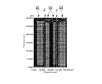
- FIG. (A) to (F) are diagrams showing simulation results of the occurrence of singularities in the liquid crystal display devices of Comparative Example 1 and Example 1-5.
- FIG. 10 is a diagram showing simulation results of the occurrence of singularities in the liquid crystal display device of Comparative Example 2 in FIGS. 9 (A) to (C).
- FIG. 12 is a diagram illustrating a simulation result of a singularity occurrence state in the liquid crystal display device of Comparative Example 3 in FIG. 11.
- the liquid crystal display device of 2nd Embodiment it is a top view which shows two adjacent sub pixels.
- production state of a singular point in the liquid crystal display device of 2nd Embodiment of FIG. It is a top view which shows two adjacent sub pixels in the liquid crystal display device of 3rd Embodiment.
- FIG. 16 is a diagram illustrating a simulation result of a singularity occurrence state in the liquid crystal display device of the third embodiment of FIG. 15.
- FIG. 10 is a plan view showing two adjacent sub-pixels in a liquid crystal display device of Comparative Example 4.
- A) and (B) are diagrams showing simulation results of the occurrence of singularities in each of the liquid crystal display device of Comparative Example 4 of FIG. 19 and the fourth embodiment of FIG.
- the liquid crystal display device of 5th Embodiment it is a top view which shows two adjacent sub pixels.
- the liquid crystal display device of the comparative example 5 it is a top view which shows two adjacent sub pixels.
- (A), (B) It is a figure which shows the simulation result of the generation
- the liquid crystal display device of 6th Embodiment it is a schematic diagram which shows the relationship between the light distribution of a backlight, the pixel arrangement
- FIG. 1 is a cross-sectional view showing the liquid crystal display device of this embodiment.
- the scale of the size may be varied depending on the component.
- the liquid crystal display device 1 includes a liquid crystal panel 13 and a backlight 8 as shown in FIG.
- the liquid crystal panel 13 includes a first polarizing plate 3, a first retardation plate 4, a liquid crystal cell 5, a second retardation plate 6, and a second polarizing plate 7.
- the backlight 8 is disposed below the liquid crystal panel 13 in FIG.
- the light emitted from the backlight 8 is modulated for each pixel by the liquid crystal panel 13, and a predetermined image, character, or the like is displayed by the light modulated for each pixel.
- the observer sees the display from the upper side of the liquid crystal display device 1 in FIG.
- the upper side of the liquid crystal display device 1 is referred to as the viewing side or the front side
- the lower side of the liquid crystal display device 1 (the side on which the backlight 8 is disposed) is referred to as the back side.
- the x axis is defined as the horizontal direction of the screen of the liquid crystal display device 1
- the y axis is defined as the vertical direction of the screen of the liquid crystal display device 1
- the z axis is defined as the thickness direction of the liquid crystal display device 1.
- liquid crystal panel 13 an active matrix transmissive liquid crystal panel is described as an example, but a liquid crystal panel applicable to the present invention is not limited to an active matrix transmissive liquid crystal panel.
- the liquid crystal panel applicable to the present invention may be, for example, a transflective (transmission / reflection type) liquid crystal panel, and each pixel is a switching thin film transistor (hereinafter abbreviated as TFT). It may be a simple matrix type liquid crystal panel that does not include
- the liquid crystal cell 5 constituting the liquid crystal panel 13 is sandwiched between a TFT substrate 9 as a switching element substrate, a color filter substrate 10 disposed opposite to the TFT substrate 9, and the TFT substrate 9 and the color filter substrate 10.
- Liquid crystal layer 11 is surrounded by a TFT substrate 9, a color filter substrate 10, and a frame-shaped sealing material (not shown) that bonds the TFT substrate 9 and the color filter substrate 10 at a predetermined interval. It is enclosed in the space.
- the liquid crystal cell 5 of the present embodiment performs display in the VA mode, and a liquid crystal having negative dielectric anisotropy is used for the liquid crystal layer 11.
- columnar spacers 12 are arranged to keep the distance between these substrates constant.
- the spacer 12 is made of resin, for example, and is formed by a photolithography technique.
- a second polarizing plate 7 functioning as a polarizer is provided on the backlight 8 side of the liquid crystal cell 5.
- a first polarizing plate 3 that functions as an analyzer is provided on the viewing side of the liquid crystal cell 5.
- a second retardation plate 6 is provided between the second polarizing plate 7 and the liquid crystal cell 5 for compensating for the phase difference of light.
- a first retardation plate 4 for compensating for a phase difference of light is provided between the first polarizing plate 3 and the liquid crystal cell 5.
- the TFT substrate 9 has a plurality of sub-pixels, which are the minimum unit area for display, arranged in a matrix.
- a plurality of source bus lines 36 are formed on the TFT substrate 9 so as to extend in parallel to each other.
- a plurality of gate bus lines 37 are formed on the TFT substrate 9 so as to extend in parallel to each other and to be orthogonal to the plurality of source bus lines 36. Therefore, a plurality of source bus lines 36 and a plurality of gate bus lines 37 are formed on the TFT substrate 9 in a lattice pattern.
- a rectangular area defined by the source bus line 36 and the gate bus line 37 is one sub-pixel 38.
- the source bus line 36 is connected to the source electrode of the TFT described later, and the gate bus line 37 is connected to the gate electrode of the TFT.
- a TFT 19 having a semiconductor layer 15, a gate electrode 16, a source electrode 17, a drain electrode 18, and the like is formed on the surface of the transparent substrate 14 constituting the TFT substrate 9 on the liquid crystal layer 11 side.
- a glass substrate can be used as the transparent substrate 14.
- a semiconductor material such as CGS (Continuous Grain Silicon), LPS (Low-temperature Poly-Silicon), ⁇ -Si (Amorphous Silicon).
- a semiconductor layer 15 is formed.
- a gate insulating film 20 is formed on the transparent substrate 14 so as to cover the semiconductor layer 15.
- a material of the gate insulating film 20 for example, a silicon oxide film, a silicon nitride film, or a laminated film thereof is used.
- a gate electrode 16 is formed on the gate insulating film 20 so as to face the semiconductor layer 15.
- a laminated film of W (tungsten) / TaN (tantalum nitride), Mo (molybdenum), Ti (titanium), Al (aluminum), or the like is used.
- a first interlayer insulating film 21 is formed on the gate insulating film 20 so as to cover the gate electrode 16.
- a material of the first interlayer insulating film 21 for example, a silicon oxide film, a silicon nitride film, or a laminated film thereof is used.
- a source electrode 17 and a drain electrode 18 are formed on the first interlayer insulating film 21.
- the source electrode 17 is connected to the source region of the semiconductor layer 15 through a contact hole 22 that penetrates the first interlayer insulating film 21 and the gate insulating film 20.
- the drain electrode 18 is connected to the drain region of the semiconductor layer 15 through a contact hole 23 that penetrates the first interlayer insulating film 21 and the gate insulating film 20.
- the same conductive material as that for the gate electrode 16 is used.
- a second interlayer insulating film 24 is formed on the first interlayer insulating film 21 so as to cover the source electrode 17 and the drain electrode 18.
- the same material as the first interlayer insulating film 21 described above or an organic insulating material is used.
- a pixel electrode 25 is formed on the second interlayer insulating film 24.
- the pixel electrode 25 is connected to the drain electrode 18 through a contact hole 26 that penetrates the second interlayer insulating film 24. Therefore, the pixel electrode 25 is connected to the drain region of the semiconductor layer 15 using the drain electrode 18 as a relay electrode.
- a transparent conductive material such as ITO (Indium Tin Oxide) or IZO (Indium Zinc Oxide) is used.
- a black matrix 30, a color filter 31, a planarizing layer 32, a counter electrode 33, and an alignment film 34 are sequentially formed on the surface of the transparent substrate 29 constituting the color filter substrate 10 on the liquid crystal layer 11 side.
- the black matrix 30 has a function of blocking the transmission of light in the inter-pixel region, and is a photo in which metal such as Cr (chromium) or Cr / Cr oxide multilayer film, or carbon particles is dispersed in a photosensitive resin. It is made of resist.
- the color filter 31 includes dyes of red (R), green (G), and blue (B), and one pixel electrode 25 on the TFT substrate 9 is any one of R, G, and B. Two color filters 31 are arranged to face each other. A region where any one of the R, G, and B color filters 31 is arranged constitutes a sub-pixel. The three subpixels R, G, and B constitute one pixel.
- the “sub-pixel” in the present embodiment corresponds to a “unit region” in the claims. In the case of a liquid crystal display device that does not have a color filter, there is no concept of a sub-pixel, so “pixel” corresponds to “unit region” in the claims.
- the flattening layer 32 is made of an insulating film that covers the black matrix 30 and the color filter 31, and has a function of smoothing and flattening a step formed by the black matrix 30 and the color filter 31.
- a counter electrode 33 is formed on the planarization layer 32. As the material of the counter electrode 33, a transparent conductive material similar to that of the pixel electrode 25 is used.
- the color filter 31 may have a multicolor configuration of three or more colors of R, G, and B. In the present embodiment, the three colors R, G, and B of the color filter 31 are aligned in the horizontal direction (x-axis direction) of the display screen of the liquid crystal panel 5 as shown in FIG.
- an alignment film 27 is formed on the entire surface of the second interlayer insulating film 24 so as to cover the pixel electrode 25.
- an alignment film 34 is formed on the entire surface covering the counter electrode 33.
- the alignment film 27 and the alignment film 34 have an alignment regulating force for vertically aligning the liquid crystal molecules 11 ⁇ / b> B constituting the liquid crystal layer 11.
- the alignment film 27 and the alignment film 34 are so-called vertical alignment films.
- the alignment film 27 and the alignment film 34 are subjected to an alignment process using a photo-alignment technique.
- the alignment film 27 on the TFT substrate 9 and the alignment film 34 on the color filter substrate 10 are subjected to alignment treatments in parallel and in opposite directions.
- the alignment film 27 on the TFT substrate 9 is subjected to an alignment process in the direction indicated by the solid arrow A (the direction from right to left in FIG. 1).
- the alignment film 34 on the color filter substrate 10 is subjected to an alignment process in the direction indicated by the dashed arrow B (the direction from the left to the right in FIG. 1).
- the liquid crystal molecules 11B constituting the liquid crystal layer 11 have the edge on the TFT substrate 9 side tilted to the right with respect to the normal direction of the surfaces of the alignment films 27 and 34, and the color filter substrate 10 side.
- each is oriented so as to incline to the left.
- the liquid crystal molecules 11B can be tilted stably.
- the liquid crystal molecules 11B are greatly tilted when a voltage is applied, triggered by the tilt of the liquid crystal molecules 11B when no voltage is applied.
- the direction in which the above-described alignment process is performed (the direction of the solid arrow A and the broken arrow B) is referred to as an alignment regulation direction.
- the orientation regulation direction referred to here is the azimuth angle direction when the TFT substrate 9 or the color filter substrate 10 is viewed from the normal direction.
- the alignment film 27 on the TFT substrate 9 has two regions having different alignment regulating directions.
- the alignment film 34 on the color filter substrate 10 has two regions having different alignment regulating directions. This point will be described later.
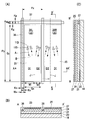
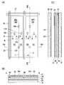
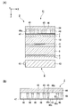
- FIG. 2A is a diagram showing the TFT substrate 9 and is a plan view showing two sub-pixels 38 adjacent to each other.
- FIG. 2B is a cross-sectional view taken along line A-A ′ of FIG.
- FIG. 2C is a cross-sectional view taken along line B-B ′ of FIG. 2B and 2C are cross-sectional views of the TFT substrate 9, and the color filter substrate 10 and the liquid crystal layer 11 are not shown.
- the wiring extending in the horizontal direction in FIG. 2A is the gate bus line 37.
- a wiring extending in the vertical direction in FIG. 2A is a source bus line 36.
- the gate bus line 37 and the source bus line 36 are orthogonal to each other.
- a rectangular area surrounded by two adjacent gate bus lines 37 and two adjacent source bus lines 36 is one sub-pixel 38.
- the above-described TFT 19 is disposed in the vicinity of the intersection of the gate bus line 37 and the source bus line 36, but the illustration is omitted in FIG.
- a rectangular pixel electrode 25 is disposed inside the sub-pixel 38 surrounded by the gate bus line 37 and the source bus line 36.
- the present inventor performed a simulation of the alignment state of the liquid crystal molecules 11B in order to verify the effect of the liquid crystal display device 1 of the present embodiment. Although the result will be described later, an example of dimensions of each part used in the simulation is shown here. Regarding the size of the sub-pixel 38, the dimension Px in the x-axis direction (direction along the gate bus line 37) is 100 ⁇ m, and the dimension Py in the y-axis direction (direction along the source bus line 36) is 300 ⁇ m. In FIG. 2A, only two adjacent sub-pixels 38 are shown, but the same structure is repeatedly arranged outside this.
- the width Wg of the gate bus line 37 is 10 ⁇ m, and the gap Kg between the gate bus line 37 and the upper and lower pixel electrodes 25 is 5 ⁇ m.
- the width Ws of the source bus line 36 is 4 ⁇ m, and the gap Ks between the source bus line 36 and the left and right pixel electrodes 25 is 3 ⁇ m.
- the dimension Gx in the x-axis direction is 90 ⁇ m, and the dimension Gy in the y-axis direction is 280 ⁇ m.
- the relative dielectric constant of the first interlayer insulating film 21 between the gate bus line 37 and the source bus line 36 shown in FIGS. 2B and 2C is 6, and the film thickness is 400 nm.
- the relative dielectric constant of the second interlayer insulating film 24 between the source bus line 36 and the pixel electrode 25 shown in FIGS. 2B and 2C is 4, and the film thickness is 2 ⁇ m.
- the left sub-pixel 38 is referred to as a first sub-pixel 38L
- the right sub-pixel 38 is referred to as a second sub-pixel 38R.
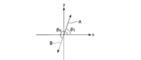
- An angle in which the orientation regulation direction of the alignment films 27 and 34 is expressed as an azimuth is defined as an orientation regulation angle.
- the orientation regulating angles ⁇ t and ⁇ c are counterclockwise with respect to the arrows A and B indicating the orientation regulating directions of the alignment films 27 and 34 with reference to the positive direction of the x axis (clockwise 3 o'clock direction). This is the angle seen around.
- the orientation restriction angle of the alignment film 27 of the TFT substrate 9 is denoted as ⁇ t
- the orientation restriction angle of the alignment film 34 of the color filter substrate 10 is denoted as ⁇ c.
- the alignment regulating direction of the alignment film 27 of the TFT substrate 9 and the alignment regulating direction of the alignment film 34 of the color filter substrate 10 are parallel and opposite to each other. For this reason, the orientation regulation angle ⁇ t and the orientation regulation angle ⁇ c are in a relationship shifted by 180 °.
- the alignment film 27 of the TFT substrate 9 has two domains having different alignment regulating directions.
- the alignment film 34 of the color filter substrate 10 has two domains having different alignment regulating directions corresponding to the alignment film 27 of the TFT substrate 9.
- D1 and a second domain D2 having an orientation regulation angle ⁇ t of 80 ° or more and less than 90 °, and an orientation regulation angle ⁇ c of 260 ° or more and less than 270 °.
- the liquid crystal molecules 11B in each of the first domain D1 and the second domain D2 are TFTs at the end on the color filter substrate 10 side.
- the substrate 9 is oriented so that it faces toward the front end of the solid arrow A indicating the orientation regulating direction of the substrate 9, and the end on the TFT substrate 9 side faces the tip side of the broken arrow B indicating the orientation regulating direction of the color filter substrate 10. That is, each of the first sub-pixel 38L and the second sub-pixel 38R has two domains D1 and D2 having different director directions of the liquid crystal molecules 11B.
- the liquid crystal molecules 11B aligned in the above-described direction are represented by conical figures as shown in FIG.
- the circular surface of the cone showing the liquid crystal molecules 11B indicates the end of the liquid crystal molecules 11B on the color filter substrate 10 side, and the sharp side indicates the end of the liquid crystal molecules 11B on the TFT substrate 9 side.
- the direction of the director of the liquid crystal molecules 11 ⁇ / b> B is represented by the direction of the director of the liquid crystal molecules 11 ⁇ / b> B located at the center in the thickness direction of the liquid crystal layer 11.
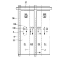
- each of the sub-pixels 38L and 38R includes the first domain D1 in which the azimuth angle component of the director of the liquid crystal molecules 11B in the central portion in the thickness direction of the liquid crystal layer 11 faces the first direction, and the thickness of the liquid crystal layer 11. And a second domain D2 in which the azimuth angle component of the director of the liquid crystal molecules 11B at the center in the vertical direction faces the second direction.
- the first direction and the second direction are non-parallel.
- the boundary line J between the first domain D1 and the second domain D2 extends in a direction parallel to the source bus line 36 (y-axis direction).
- the boundary line J is at a position shifted from the center of each of the sub-pixels 38L and 38R, and the size of the first domain D1 is different from the size of the second domain D2.
- the pixel electrode 25 having a width of 90 ⁇ m is divided into two by the boundary line J.
- the width M1 of the first domain D1 is 60 ⁇ m
- the width M2 of the second domain D2 is 30 ⁇ m.
- the first sub-pixel 38L the first domain D1 is disposed on the left side
- the second domain D2 is disposed on the right side.
- the second sub-pixel 38R the first domain D1 is disposed on the right side
- the second domain D2 is disposed on the left side.
- the first domain D1 and the second domain D2 are symmetrically arranged around the boundary line H between the first sub-pixel 38L and the second sub-pixel 38R. Yes. Further, with this arrangement, when the first sub-pixel 38L and the second sub-pixel 38R are combined, the width M1 of the first domain D1 and the width M2 of the second domain D2 are substantially equal. Such a configuration simplifies the configuration of a mask used when performing photo-alignment processing on the alignment films 27 and 34.
- the alignment direction of the liquid crystal molecules 11B is as described above with respect to the azimuth direction in plan view of the liquid crystal panel 13.
- the so-called pretilt angle ⁇ p formed by the director surface of the liquid crystal molecules 11B when no voltage is applied is 88 °.
- the twist angle of the liquid crystal molecules 11B is 0 °. That is, in the present embodiment, the liquid crystal molecules 11B are not twisted in the thickness direction of the liquid crystal layer 11.
- the transmission axes of the two polarizing plates 3 and 7 sandwiching the liquid crystal layer 11 were arranged in a crossed Nicols orientation of 0 ° -180 ° and 90 ° -270 °.
- the gate voltage was set to -12V
- the source voltage was set to 0V
- the common voltage was set to 0V.
- the voltage applied to the pixel electrode 25 was changed from 0V to + 7V in 1V steps.
- the voltage applied to the pixel electrode 25 was changed from 0V to -7V in -1V steps.
- FIG. 4 is a plan view showing two adjacent sub-pixels in the liquid crystal display device of Comparative Example 1.
- FIG. 4 the same components as those in FIG. 2A are denoted by the same reference numerals, and description thereof is omitted.
- each of the sub-pixels 38L and 38R has two domains, but the direction of the director of the liquid crystal molecules 11B in the first domain D1 and the liquid crystal molecules in the second domain D2.
- the direction of the director of 11B is parallel.
- the direction of the director of the liquid crystal molecules 11B is parallel to the domain boundary line J.
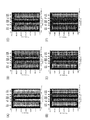
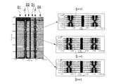
- FIGS. 5A to 5F are diagrams showing simulation results of the alignment state of liquid crystal molecules when a voltage is applied, for the liquid crystal display device of the present embodiment and the liquid crystal display device of Comparative Example 1.
- FIG. FIG. 5A shows a simulation result of the liquid crystal display device of Comparative Example 1.
- FIGS. 5B to 5F show simulation results of the liquid crystal display device of the present embodiment, and show results when the alignment regulation angles of the alignment films are changed within the range of the present embodiment. .
- the orientation restriction angle ⁇ t of the first domain D1 is 271 °
- the orientation restriction angle ⁇ c of the first domain D1 is 91 °. That is, the direction of the director of the liquid crystal molecules 11B in the first domain D1 is a 91 ° -271 ° direction.
- the orientation restriction angle ⁇ t of the second domain D2 was 89 °
- the orientation restriction angle ⁇ c of the second domain D2 was 269 °. That is, the direction of the director of the liquid crystal molecules 11B in the second domain D2 is the 89 ° -269 ° direction.
- the angle formed between the director direction of the liquid crystal molecules 11B in the first domain D1 and the director direction of the liquid crystal molecules 11B in the second domain D2 is 2 ° ( ⁇ 1 ° centering on the boundary line J).
- This liquid crystal display device is referred to as the liquid crystal display device of Example 1.
- the direction of the director of the liquid crystal molecules 11B in the first domain D1 is a 92 ° -272 ° direction.
- the direction of the director of the liquid crystal molecules 11B in the second domain D2 is 88 ° -268 °. Therefore, the angle formed by the director direction of the liquid crystal molecules 11B in the first domain D1 and the director direction of the liquid crystal molecules 11B in the second domain D2 is 4 ° ( ⁇ 2 ° centering on the boundary line J).
- This liquid crystal display device is a liquid crystal display device of Example 2.
- the direction of the director of the liquid crystal molecules 11B in the first domain D1 is 93 ° -273 °.
- the direction of the director of the liquid crystal molecules 11B in the second domain D2 is 87 ° -267 °. Therefore, the angle formed between the director direction of the liquid crystal molecules 11B in the first domain D1 and the director direction of the liquid crystal molecules 11B in the second domain D2 is 6 ° ( ⁇ 3 ° centering on the boundary line J).
- This liquid crystal display device is a liquid crystal display device of Example 3.
- the direction of the director of the liquid crystal molecules 11B in the first domain D1 is 95 ° -275 °.
- the direction of the director of the liquid crystal molecules 11B in the second domain D2 is the 85 ° -265 ° direction. Therefore, the angle formed between the director direction of the liquid crystal molecules 11B in the first domain D1 and the director direction of the liquid crystal molecules 11B in the second domain D2 is 10 ° ( ⁇ 5 ° centering on the boundary line J).
- This liquid crystal display device is a liquid crystal display device of Example 4.
- the direction of the director of the liquid crystal molecules 11B in the first domain D1 is the direction of 100 ° -280 °.
- the direction of the director of the liquid crystal molecules 11B in the second domain D2 is an 80 ° -260 ° direction. Therefore, the angle formed between the director direction of the liquid crystal molecules 11B in the first domain D1 and the director direction of the liquid crystal molecules 11B in the second domain D2 is 20 ° ( ⁇ 10 ° centering on the boundary line J).
- This liquid crystal display device is a liquid crystal display device of Example 5.
- the director direction of the liquid crystal molecules 11B in D1 and the director direction of the liquid crystal molecules 11B in the second domain D2 change from a parallel state to a direction in which the spread in the two director directions increases.
- the light transmittance can be expressed by the following equation (1).
- equation (1) when considering the influence of the change in the alignment direction of the liquid crystal molecules 11B on the light transmittance, only the angle ⁇ between the transmission axis of the polarizing plate and the director direction of the liquid crystal molecules in the following formula (1). Changes, and the refractive index anisotropy ⁇ n of the liquid crystal, the thickness d of the liquid crystal, and the wavelength ⁇ of light are considered to be constant. In that case, the influence of the change in the alignment direction of the liquid crystal molecules 11B on the light transmittance can be expressed by the following equation (2).
- the transmission axes of the pair of polarizing plates are arranged in crossed Nicols in the 45 ° -225 ° direction and the 135 ° -315 ° direction of FIGS. 5 (A) to (F).
- the liquid crystal display device of Comparative Example 1 in FIG. 5A in which the transmission axis of the polarizing plate and the direction of the director of the liquid crystal molecules form an angle of 45 ° is the maximum.
- the liquid crystal display devices of Examples 1 to 5 in FIGS. 5B to 5F are inferior to the liquid crystal display device of Comparative Example 1.
- the angle between the transmission axis of the polarizing plate and the direction of the director of the liquid crystal molecules deviates from 45 °, so that the light transmittance decreases.
- the angle formed by the director direction of the liquid crystal molecules is preferably 6 ° or more and 20 ° or less.
- FIG. 6 is an enlarged view of the vicinity of the three singular points of the first sub-pixel 38L in the simulation result of the comparative example 1 shown in FIG.
- FIG. 7 is an enlarged view of a region where no singular point is generated in the first sub-pixel 38L in the simulation result of the fourth embodiment illustrated in FIG.
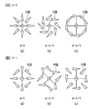
- FIGS. 8A-(a) to (c) and FIGS. 8 (B)-(a) to (c) there are several types of singular points depending on the alignment state of the liquid crystal molecules 11B.
- FIGS. 8A- (a) to (c) and FIGS. 8B- (a) to (c) are schematic views of the alignment state of the liquid crystal molecules 11B as viewed from the normal direction of the liquid crystal panel.
- the singular points include a singular point called the first singular point shown in FIGS. 8 (A)-(a) to (c) and a second singular point shown in FIGS. 8 (B)-(a)-(c). There are singularities called points.
- the first singular point is basically a singular point in which one end of all the liquid crystal molecules 11B is oriented to the same point.
- the second singular point is basically that one end of the liquid crystal molecules arranged along one arbitrary direction is directed to the same point, but other liquid crystal molecules, for example, liquid crystal molecules arranged along the direction orthogonal to the one direction.
- One end of is a singular point that takes an orientation state that does not go to the same point.
- the first singular point is denoted as +1 and the second singular point is denoted as -1.
- the liquid crystal molecules 11B are arranged so as to be largely rotated around the singular point.
- FIGS. 8B- (a) to (c) an angle ⁇ formed between an axis connecting the singular point of ⁇ 1 and the liquid crystal molecule 11B and the director of the liquid crystal molecule 11B.
- This is the same as the conventional MVA liquid crystal display device.
- FIG. 9A is a plan view showing two adjacent sub-pixels of a liquid crystal display device using the conventional MVA technology.
- FIG. 9B is a cross-sectional view taken along the line AA ′ of FIG.
- FIG. 9C is a cross-sectional view taken along the line BB ′ in FIG.
- the liquid crystal display device shown in FIGS. 9A to 9C is referred to as a liquid crystal display device of Comparative Example 2.
- openings 25h and 33h are provided in the pixel electrode 25 and the counter electrode 33, respectively, as means for regulating the alignment of the liquid crystal molecules 11B.
- a total of three openings 25h and 33h are arranged along the boundary line J between the two domains.
- the two upper and lower openings 25h are provided in the pixel electrode 25 shown in FIG.
- One central opening 33h is an opening provided in the counter electrode 33 shown in FIG.
- the dimensions of the openings 25h and 33h were all 10 ⁇ m square.
- the direction of the director of the liquid crystal molecules 11B in the two domains D1 and D2 is the same as that of the liquid crystal display device of Comparative Example 1.
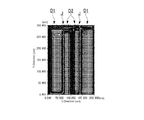
- FIG. 10 is a diagram illustrating a simulation result of the alignment state of the liquid crystal molecules when a voltage is applied to the liquid crystal display device of Comparative Example 2.
- the singular point cannot be eliminated and the position of the singular point cannot be fixed.
- FIG. 11 is a plan view showing two adjacent sub-pixels in a liquid crystal display device in which the director direction of the liquid crystal molecules 11B is perpendicular to the domain boundary line J.
- FIG. 11 The liquid crystal display device shown in FIG. 11 is referred to as a liquid crystal display device of Comparative Example 3.
- the upper and lower openings 33h are openings provided in the counter electrode 33 as shown in FIG.
- One central opening 25 h is an opening provided in the pixel electrode 25.
- the dimensions of the openings 33h and 25h were all 10 ⁇ m square.
- the orientation regulation angle ⁇ t of the first domain D1 was 0 °
- the orientation regulation angle ⁇ c of the first domain D1 was 180 °. That is, the director direction of the liquid crystal molecules 11B in the first domain D1 is the 0 ° -180 ° direction.
- the orientation restriction angle ⁇ t of the second domain D2 was 180 °
- the orientation restriction angle ⁇ c of the second domain D2 was 0 °. That is, the director direction of the liquid crystal molecules 11B in the second domain D2 is the 0 ° -180 ° direction. Therefore, the director direction of the liquid crystal molecules 11B in the first domain D1 and the director direction of the liquid crystal molecules 11B in the second domain D2 are parallel.
- FIG. 12 is a diagram illustrating a simulation result of the alignment state of liquid crystal molecules when a voltage is applied to the liquid crystal display device of Comparative Example 3.
- the position of the singular point can be fixed.
- singularities cannot be eliminated.
- the two domains D1 and D2 are provided in one subpixel 38, and the direction of the director of the liquid crystal molecules 11B in the two domains D1 and D2 is Non-parallel.
- the singular points can be reduced or the singular points can be eliminated without providing orientation regulating means such as electrode openings and protrusions. In this manner, a liquid crystal display device having excellent display characteristics can be realized without complicating the manufacturing process.
- FIG. 13 is a plan view showing two adjacent sub-pixels in the liquid crystal display device of the present embodiment.
- FIG. 14 is a diagram illustrating a simulation result of the alignment state of liquid crystal molecules when a voltage is applied to the liquid crystal display device of the present embodiment.
- symbol is attached
- the orientation regulation angle ⁇ t is greater than 270 ° and 280 ° or less, and the orientation regulation angle ⁇ c is greater than 90 °. And 100 ° or less.
- the orientation regulation angle ⁇ t is 90 °, and the orientation regulation angle ⁇ c is 270 °. That is, in the liquid crystal display device of this embodiment, the director direction of the liquid crystal molecules 11B is non-parallel to the domain boundary line J only in the first domain D1. For the second domain D2, the director direction of the liquid crystal molecules 11B is parallel to the domain boundary line J.
- FIG. 14 is a diagram illustrating a simulation result of the alignment state of liquid crystal molecules when a voltage is applied to the liquid crystal display device of the present embodiment.
- the simulation conditions were such that the orientation restriction angle ⁇ t of the first domain D1 was 275 °, and the orientation restriction angle ⁇ c of the first domain D1 was 95 °. That is, the director direction of the liquid crystal molecules 11B in the first domain D1 is a 95 ° -275 ° direction.
- the director direction of the liquid crystal molecules 11B in the second domain D2 is a 90 ° -270 ° direction. Therefore, the angle formed by the director direction of the liquid crystal molecules 11B in the first domain D1 and the director direction of the liquid crystal molecules 11B in the second domain D2 is 5 °.
- FIG. 15 is a plan view showing two adjacent sub-pixels in the liquid crystal display device of the present embodiment.
- FIG. 16 is a diagram showing a simulation result of the alignment state of the liquid crystal molecules when a voltage is applied in the liquid crystal display device of the present embodiment.
- FIG. 17 is a plan view showing two adjacent sub-pixels in a liquid crystal display device according to a modification of the present embodiment. 15 to 17, the same reference numerals are given to the same components as those used in the first embodiment, and detailed description thereof will be omitted.
- the orientation regulation angle ⁇ t is greater than 270 ° and not more than 280 °, and the orientation regulation angle ⁇ c is 90 °.
- the orientation regulation angle ⁇ t is 80 ° or more and smaller than 90 °, and the orientation regulation angle ⁇ c is 270 °. That is, in the liquid crystal display device of the present embodiment, the liquid crystal molecules 11B are twisted at an angle of 10 ° or less in each of the first domain D1 and the second domain D2.
- FIG. 16 is a diagram showing a simulation result of the alignment state of the liquid crystal molecules when a voltage is applied in the liquid crystal display device of the present embodiment.
- the simulation conditions were such that the orientation restriction angle ⁇ t of the first domain D1 was 280 ° and the orientation restriction angle ⁇ c of the first domain D1 was 90 °. That is, the liquid crystal molecules 11 ⁇ / b> B in the first domain D ⁇ b> 1 are twisted by 10 ° in the thickness direction of the liquid crystal layer 11.
- the director direction of the liquid crystal molecules 11B at the center in the thickness direction of the liquid crystal layer 11 can be regarded as a 95 ° -275 ° direction.
- the orientation restriction angle ⁇ t of the second domain D2 was 80 °
- the orientation restriction angle ⁇ c of the second domain D2 was 270 °. That is, the liquid crystal molecules 11B in the second domain D2 are twisted by ⁇ 10 ° in the thickness direction of the liquid crystal layer 11.
- the director direction of the liquid crystal molecules 11B at the center in the thickness direction of the liquid crystal layer 11 can be regarded as the 85 ° -265 ° direction.
- the liquid crystal molecules 11B that are most likely to move when a voltage is applied in the liquid crystal layer 11 are liquid crystal molecules 11B that are not constrained by the alignment films 27 and 34 on the surface of the substrate and are located in the center in the thickness direction of the liquid crystal layer 11.
- the liquid crystal molecules 11B by twisting the liquid crystal molecules 11B, an angle is given to the liquid crystal molecules 11B in the central portion in the thickness direction of the liquid crystal layer 11 in the two domains D1 and D2, and the same action as in the first and second embodiments. , Have an effect.
- the same effect as the first and second embodiments can be obtained that a liquid crystal display device having excellent display characteristics can be realized without complicating the manufacturing process.
- the alignment restriction angle ⁇ c on the color filter substrate 10 side is made parallel to the domain boundary line J, and the alignment restriction angle ⁇ t on the TFT substrate 9 side is made non-parallel to the domain boundary line J.
- the orientation regulation angle ⁇ t on the TFT substrate 9 side may be parallel to the domain boundary line J, and the orientation regulation angle ⁇ c on the color filter substrate 10 side may be non-parallel to the domain boundary line J.
- the orientation regulation angle ⁇ t is 270 °
- the orientation regulation angle ⁇ c is greater than 90 °, and is 100 ° or less. It is.
- the orientation regulation angle ⁇ t is 90 °
- the orientation regulation angle ⁇ c is 260 ° or more and smaller than 270 °. That is, in the liquid crystal display device of this modification, the liquid crystal molecules 11B are twisted at an angle of 10 ° or less in each of the first domain D1 and the second domain D2. Also in the liquid crystal display device of this modification, the simulation result is substantially the same as FIG.
- FIG. 18 is a plan view showing two adjacent sub-pixels in the liquid crystal display device of the present embodiment.
- FIG. 19 is a plan view showing two adjacent sub-pixels in the liquid crystal display device of Comparative Example 4.
- FIG. 20A is a diagram illustrating a simulation result of the alignment state of liquid crystal molecules when a voltage is applied to the liquid crystal display device of Comparative Example 4.
- 20B is a diagram showing a simulation result of the alignment state of the liquid crystal molecules when a voltage is applied to the liquid crystal display device of this embodiment.
- 18 to 20 the same reference numerals are given to the same components as those used in the first embodiment, and the detailed description thereof will be omitted.
- the orientation regulation angle ⁇ t is greater than 0 ° and 10 ° or less, and the orientation regulation angle ⁇ c is greater than 180 °. And 190 ° or less.
- the orientation regulation angle ⁇ t is 170 ° or more and less than 180 °, and the orientation regulation angle ⁇ c is 350 ° or more and less than 360 °.
- the orientation restriction angle ⁇ t was set to 5 °
- the orientation restriction angle ⁇ c was set to 185 °.
- the director direction of the liquid crystal molecules 11B in the first domain D1 is the 5 ° -185 ° direction.
- the orientation regulation angle ⁇ t is 175 °
- the orientation regulation angle ⁇ c is 355 °.
- the director direction of the liquid crystal molecules 11B in the second domain D2 is the 175 ° -355 ° direction. Therefore, the angle formed by the director direction of the liquid crystal molecules 11B in the two domains D1 and D2 is 10 °.
- the orientation regulation angle ⁇ t was 0 ° and the orientation regulation angle ⁇ c was 180 °.
- the director direction of the liquid crystal molecules 11B in the first domain D1 is the 0 ° -180 ° direction.
- the orientation regulation angle ⁇ t is 180 °
- the orientation regulation angle ⁇ c is 0 °.
- the director direction of the liquid crystal molecules 11B in the second domain D2 is the 0 ° -180 ° direction. That is, the director directions of the liquid crystal molecules 11B in the two domains D1 and D2 are parallel.
- FIG. 20A in the case of the liquid crystal display device of Comparative Example 4, many singular points (locations indicated by arrows) are generated.
- FIG. 20B in the case of the liquid crystal display device of this embodiment, the number of singular points is reduced to one. Also in the present embodiment, it has been found that the liquid crystal molecules 11B are aligned in an arc based on the director direction of the liquid crystal molecules 11B regulated in the adjacent domains D1 and D2. Therefore, a singular point is less likely to occur in the liquid crystal display device of this embodiment.
- the same effect as in the first to third embodiments can be obtained that a liquid crystal display device having excellent display characteristics can be realized without complicating the manufacturing process.
- FIG. 21 is a plan view showing two adjacent sub-pixels in the liquid crystal display device of the present embodiment.
- FIG. 22 is a plan view showing two adjacent sub-pixels in the liquid crystal display device of Comparative Example 5.
- FIG. 23A is a diagram illustrating a simulation result of the alignment state of liquid crystal molecules when a voltage is applied to the liquid crystal display device of Comparative Example 5.
- 23B is a diagram showing a simulation result of the alignment state of liquid crystal molecules when a voltage is applied, in the liquid crystal display device of this embodiment. 21 to 23, the same reference numerals are given to the same components as those used in the first embodiment, and the detailed description thereof will be omitted.
- the boundary line J between the first domain D1 and the second domain D2 extends in a direction parallel to the gate bus line 37 (x-axis direction).
- the first domain D1 and the second domain D2 are arranged side by side in a direction parallel to the source bus line 36 (y-axis direction).
- the boundary line J between the two domains D1 and D2 is at a position shifted from the center of each sub-pixel 38, and the size of the first domain D1 located on the pixel electrode 25 is different from the size of the second domain D2.
- the pixel electrode 25 whose dimension Gy in the y-axis direction (longitudinal direction) is 280 ⁇ m is divided into two by the boundary line J.
- the dimension N1 in the y-axis direction of the first domain D1 is 190 ⁇ m
- the dimension N2 in the y-axis direction of the second domain D2 is 90 ⁇ m.
- the orientation regulation angle ⁇ t in the first domain D1, the orientation regulation angle ⁇ t is 350 ° or more and less than 360 °, and the orientation regulation angle ⁇ c is 170 ° or more and less than 180 °.
- the orientation regulation angle ⁇ t in the second domain D2, the orientation regulation angle ⁇ t is greater than 180 ° and 190 ° or less, and the orientation regulation angle ⁇ c is greater than 0 ° and 10 ° or less.
- the orientation restriction angle ⁇ t is 355 °
- the orientation restriction angle ⁇ c is 175 °.
- the direction of the director of the liquid crystal molecules 11B in the first domain D1 is 175 ° -355 °.
- the orientation regulation angle ⁇ t is 185 °
- the orientation regulation angle ⁇ c is 5 °.
- the direction of the director of the liquid crystal molecules 11B in the second domain D2 is the 5 ° -185 ° direction. Therefore, the angle formed by the director of the liquid crystal molecules 11B in the two domains D1 and D2 is 10 °.
- the orientation regulation angle ⁇ t was 0 ° and the orientation regulation angle ⁇ c was 180 °.
- the direction of the director of the liquid crystal molecules 11B in the first domain D1 is the 0 ° -180 ° direction.
- the orientation regulation angle ⁇ t is 180 °
- the orientation regulation angle ⁇ c is 0 °.
- the direction of the director of the liquid crystal molecules 11B in the second domain D2 is the 0 ° -180 ° direction. That is, the directions of the directors of the liquid crystal molecules 11B in the two domains D1 and D2 are parallel.
- the same effect as in the first to fifth embodiments can be obtained that a liquid crystal display device having excellent display characteristics can be realized without complicating the manufacturing process.
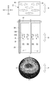
- FIG. 24 is a perspective view of the liquid crystal display device of the present embodiment.
- FIG. 25A is a cross-sectional view of a liquid crystal display device
- FIG. 25B is a cross-sectional view of a light diffusion film.
- FIG. 26 is a diagram for explaining the arrangement relationship among the backlight, the liquid crystal panel, and the light diffusion film. 24 to 26, the same reference numerals are given to the same components as those used in the first embodiment, and detailed description thereof will be omitted.
- the liquid crystal display device 41 of the present embodiment includes a backlight 8, a liquid crystal panel 13, and a light diffusion film 2 (light diffusion member).
- the liquid crystal panel 13 includes a first polarizing plate 3, a first retardation plate 4, a TFT substrate 9 and a color filter substrate 10 that sandwich the liquid crystal layer 11 and the color filter 31, a second retardation plate 6, and a second retardation plate 6. And a polarizing plate 7.
- each of the TFT substrate 9 and the color filter substrate 10 is schematically illustrated as a single plate, but the detailed structure is as described in the first embodiment ( (See FIG. 1).
- the observer sees the display from the upper side of the liquid crystal display device 41 in FIG. 24 where the light diffusion film 2 is arranged. Therefore, in the following description, the side on which the light diffusion film 2 is disposed is referred to as a viewing side, and the side on which the backlight 8 is disposed is referred to as a back side.
- the light emitted from the backlight 8 is modulated by the liquid crystal panel 13, and a predetermined image, text, or the like is displayed by the modulated light.
- the angle distribution of the emitted light becomes wider than before entering the light diffusing film 2, and the light is emitted from the light diffusing film 2. Thereby, the observer can visually recognize the display with a wide viewing angle.
- the backlight 8 may be an edge light type backlight in which a light source 42 such as an LED is disposed on the end face of the light guide 43, or the light source is directly below the light guide. It may be a direct type backlight disposed in the. As the backlight 8, it is desirable to use a backlight having a directivity by controlling the light emission direction, that is, a so-called directional backlight. By using a directional backlight capable of entering parallel light into a light diffusion portion of the light diffusion film 2 described later, display blur can be reduced and light utilization efficiency can be increased. The light distribution of the backlight will be described later.
- the light diffusing film 2 includes a transparent base 44 and a plurality of light shielding portions 45 formed on one surface of the transparent base 44 (the surface opposite to the viewing side). And a light diffusing portion 46 formed on one surface of the transparent substrate 44.
- the light diffusing film 2 is a first polarized light with the side where the light diffusing portion 46 is provided facing the first polarizing plate 3 and the side of the transparent substrate 44 facing the viewing side. It is fixed on the plate 3 by an adhesive layer 47.
- the transparent substrate 44 is made of a transparent resin such as a triacetyl cellulose (TAC) film, polyethylene terephthalate (PET), polycarbonate (PC), polyethylene naphthalate (PEN), or polyethersulfone (PES) film. Is preferably used.
- the transparent base material 44 is a base for applying the material of the light shielding part 45 and the light diffusion part 46 in the manufacturing process, and needs to have heat resistance and mechanical strength in the heat treatment step during the manufacturing process. is there. Therefore, for the transparent substrate 44, a glass substrate or the like may be used in addition to the resin substrate. In this embodiment, a transparent resin substrate having a thickness of 100 ⁇ m is used as an example.
- the plurality of light shielding portions 45 are formed so as to be scattered on one surface (surface opposite to the viewing side) of the transparent base material 44.
- the planar shape of the light shielding part 45 when the light diffusing film 2 is viewed from the z-axis direction is, for example, a major axis and a minor axis represented by an ellipse. It has an anisotropic figure. That is, the shape of the light shielding layer 45 is large in the direction of the azimuth angle 0 ° -180 ° and small in the direction of the azimuth angle 90 ° -270 °.
- the side area of the light diffusion portion 46 in the azimuth angle 0 ° -180 ° direction is larger than the side area of the light diffusion portion 46 in the azimuth angle 90 ° -270 ° direction. small. Therefore, in the light diffusing film 2, the amount of light emitted and diffused in the direction of azimuth angle 0 ° -180 ° is relatively small, and the amount of light emitted diffused in the direction of azimuth angle 90 ° -270 ° is relatively small. To be more. That is, anisotropic light diffusivity is realized depending on the orientation.
- the light shielding portions 45 are drawn with the same size, but the light shielding portions 45 are not particularly limited to a certain size, and light shielding portions 45 of various dimensions may be mixed. Furthermore, the arrangement of the light shielding portions 45 is not limited to a regular arrangement, and is not limited to a periodic arrangement. That is, the light shielding portions 45 may be arranged at random. Adjacent light shielding portions 45 may be formed to overlap each other.
- the light-shielding portion 45 is composed of a layer made of a black pigment, dye, resin or the like having light absorption and photosensitivity such as a black resist containing carbon black.
- a resin containing carbon black or the like the film constituting the light shielding portion 45 can be formed in the printing process, so that advantages such as a small amount of material used and a high throughput can be obtained.
- a metal film such as Cr (chromium) or a Cr / Cr oxide multilayer film may be used. When this type of metal film or multilayer film is used, the optical density of these films is high, so that there is an advantage that light is sufficiently absorbed by the thin film.
- the light diffusing section 46 is made of an organic material having optical transparency and photosensitivity such as acrylic resin and epoxy resin.
- the thickness of the light diffusion portion 46 is set to be sufficiently larger than the thickness of the light shielding portion 45.
- the thickness of the light diffusing portion 46 is about 25 ⁇ m as an example, and the thickness of the light shielding portion 45 is about 150 nm as an example.
- the cross-sectional area when cut along a plane parallel to the one surface of the transparent base material 39 is large on the light shielding portion 45 side, and gradually decreases as the distance from the light shielding portion 45 increases.
- a hollow portion 48 having a shape is formed. That is, the hollow portion 48 has a so-called forward tapered frustoconical shape when viewed from the transparent substrate 44 side. Air exists in the hollow portion 48.
- the light diffusion part 46 is an area where the transparent resin is continuously present, and contributes to the transmission of light.
- the light that has entered the light diffusing portion 46 is totally reflected at the side surface 46 c of the light diffusing portion 46, that is, the interface between the light diffusing portion 46 and the hollow portion 48, and proceeds inside the light diffusing portion 46, and passes through the transparent substrate 44. Through the outside.
- the light diffusion portion 46 since air exists in the hollow portion 48, if the light diffusion portion 46 is formed of, for example, a transparent acrylic resin, the side surface 46c of the light diffusion portion 46 is an interface between the transparent acrylic resin and air. It becomes.
- the difference in refractive index between the inside and the outside of the light diffusing portion 46 is greater when the hollow portion 48 is filled with air than when it is filled with other general low refractive index materials. large. Therefore, in the case of this embodiment, the incident angle range in which light is totally reflected by the side surface 46c of the light diffusing portion 46 is widened according to Snell's law. As a result, light loss is further suppressed, and high luminance can be obtained.
- the hollow portion 48 may be filled with an inert gas such as nitrogen instead of air. Alternatively, the inside of the hollow portion 48 may be in a reduced pressure state.
- the surface with the smaller area becomes the light emitting end surface 46a, and the surface with the larger area.
- the surface (the surface opposite to the transparent substrate 44) is the light incident end surface 46b.
- the inclination angle ⁇ (angle formed between the light incident end face 46b and the side face 46c) of the side face 46c of the light diffusing part 46 (interface between the light diffusing part 46 and the hollow part 48) is preferably about 60 ° to 90 °.
- the inclination angle of the side surface 46c of the light diffusing portion 46 is not particularly limited as long as the loss of incident light is not so large and the incident light can be sufficiently diffused.
- a light shielding part 45 having light absorptivity is provided in a region other than the light diffusion part 46. Therefore, the light transmitted through the side surface 46 c of the light diffusion portion 46 without being totally reflected is absorbed by the light shielding portion 45. As a result, there is no possibility of blurring of display due to stray light or the like, or a decrease in contrast. On the other hand, when the amount of light transmitted through the side surface 46c of the light diffusing unit 46 increases, the amount of light emitted to the viewing side decreases, and an image with high luminance cannot be obtained.
- a backlight that emits light at an angle that does not enter the side surface 46c of the light diffusing portion 46 at a critical angle or less, that is, a so-called directional backlight.
- liquid crystal display device 41 configured as described above, the arrangement relationship among the backlight 8, the liquid crystal panel 13, and the light diffusion film 2 will be described.
- a technique for forming four domains in which the directions of directors of liquid crystal molecules are orthogonal to each other is well known and has a track record of mass production.
- this technique is referred to as a four-domain technique.
- the technology for forming two domains in which the director directions of the liquid crystal molecules are opposite to each other has not been produced so far.
- This technique is called a two-domain technique. The reason is that the four-domain technology is more advantageous than the two-domain technology when viewing angle characteristics in all directions are considered.
- a liquid crystal display device using the four-domain technology is a liquid crystal display device using the two-domain technology. It is two points of the point that manufacture is easier.
- the present inventors recently developed the above-described light diffusion film, so that when the light diffusion film is combined with the liquid crystal display device using the two-domain technology, the viewing angle characteristic is a liquid crystal using the four-domain technology. It has been found that this is an improvement over display devices. That is, the liquid crystal display device using the four-domain technology has substantially uniform viewing angle characteristics with respect to the four directions, whereas the liquid crystal display device using the two-domain technology has the four-domain technology only in the two directions. The viewing angle characteristics in the remaining two directions were inferior while the viewing angle characteristics were superior to the above. Therefore, by using a light diffusing film having anisotropic light diffusibility, the viewing angle characteristics in two directions on the bad side can be improved, thereby realizing excellent viewing angle characteristics in all directions.
- the backlight 8 having a light distribution in which the luminance change in the 0 ° -180 ° direction is gentle and the luminance change in the 90 ° -270 ° direction is steep. Deploy.
- the backlight 8 is arranged so that the direction in which the directivity of emitted light is high (the direction indicated by the arrow P) is in the 90 ° -270 ° direction.
- the boundary line J between the two domains D1 and D2 is parallel to the 90 ° -270 ° direction, as shown in FIG. 2A of the first embodiment.
- the liquid crystal panel 13 is arranged so that In this case, the degree of change in light transmittance is greater in the 90 ° -270 ° direction (the direction indicated by the arrow Q) than in the 0 ° -180 ° direction. Therefore, as shown in the upper side of FIG. 26, the major axis direction of the light shielding part 45 is oriented in the 0 ° -180 ° direction, and the minor axis direction of the light shielding part 45 is in the direction of 90 ° -270 ° (direction indicated by the arrow R).
- the light diffusion film 2 is arranged so as to face.
- the light diffusion film 2 has a diffusion intensity that varies depending on the azimuth angle direction, and an azimuth angle direction (a direction indicated by an arrow R) in which the diffusion intensity is relatively large is an azimuth angle direction in which the transmittance change in the liquid crystal panel 13 is relatively large. (Direction indicated by arrow Q) is substantially the same.
- the proportion of light diffused in the 90 ° -270 ° direction is larger than the proportion of light diffused in the 0 ° -180 ° direction.
- a steep change in light transmittance in the 90 ° -270 ° direction is alleviated, and excellent viewing angle characteristics are realized in all directions.
- the technical scope of the present invention is not limited to the above embodiment, and various modifications can be made without departing from the spirit of the present invention.
- the first embodiment an example is given in which liquid crystal molecules are not twisted between a pair of substrates sandwiching a liquid crystal layer.
- the third embodiment an example in which the liquid crystal molecules are twisted by 10 ° between a pair of substrates sandwiching the liquid crystal layer has been described.
- the twist angle of the liquid crystal molecules is not necessarily limited to 10 ° and can be set as appropriate.
- the twist angle of the liquid crystal molecules is too large, the line symmetry of viewing angle characteristics is lost in the two-domain technique. In that case, realization of 6th Embodiment combined with the light-diffusion film becomes difficult. Therefore, it is desirable that the twist angle of the liquid crystal molecules be smaller than 45 °.
- the configuration has two domains in one subpixel.
- one subpixel is arranged in the same direction so that the boundary lines of the domains are parallel to each other. It is good also as a structure divided into 4 and arrange
- This configuration has four domains, but is different from the conventional four-domain technology in which domain boundaries are orthogonal to each other. Even in that case, the same effect as the above-described embodiment can be obtained.
- the area of the 1st domain D1 showed the example larger than the area of the 2nd domain D2 in the said embodiment, the area of a domain does not necessarily need to differ and may be the same.
- the number, arrangement, dimensions, materials, and the like of the components of the liquid crystal display device are not limited to those disclosed in the above embodiment, and can be changed as appropriate.
- the present invention is applicable to a liquid crystal display device used in a display unit of various electronic devices.
Landscapes
- Physics & Mathematics (AREA)
- Nonlinear Science (AREA)
- Mathematical Physics (AREA)
- Chemical & Material Sciences (AREA)
- Crystallography & Structural Chemistry (AREA)
- General Physics & Mathematics (AREA)
- Optics & Photonics (AREA)
- Spectroscopy & Molecular Physics (AREA)
- Liquid Crystal (AREA)
Abstract
Description
以下、本発明の第1実施形態について、図1~図12を用いて説明する。
本実施形態の液晶表示装置は、1つのサブ画素内に2つのドメインを有するVAモードの液晶表示装置の一例である。
図1は、本実施形態の液晶表示装置を示す断面図である。
なお、以下の各図面においては各構成要素を見やすくするため、構成要素によって寸法の縮尺を異ならせて示すことがある。
ここでは、アクティブマトリクス方式の透過型液晶パネルを一例に挙げて説明するが、本発明に適用可能な液晶パネルはアクティブマトリクス方式の透過型液晶パネルに限るものではない。本発明に適用可能な液晶パネルは、例えば半透過型(透過・反射兼用型)液晶パネルであっても良く、更には、各画素がスイッチング用薄膜トランジスタ(Thin Film Transistor, 以下、TFTと略記する)を備えていない単純マトリクス方式の液晶パネルであっても良い。
なお、TFTの形態としては、図2に示したトップゲート型TFTであっても良いし、ボトムゲート型TFTであっても良い。
本実施形態の場合、カラーフィルター31の3色であるR,G,Bは、図1に示すように、液晶パネル5の表示画面の水平方向(x軸方向)に並んでいる。
図1には現れないが、TFT基板9上の配向膜27は、配向規制方向が互いに異なる2つの領域を有している。同様に、カラーフィルター基板10上の配向膜34は、配向規制方向が互いに異なる2つの領域を有している。この点については後述する。
サブ画素38のサイズは、x軸方向(ゲートバスライン37に沿う方向)の寸法Pxが100μmであり、y軸方向(ソースバスライン36に沿う方向)の寸法Pyが300μmである。図2(A)では、隣り合う2つのサブ画素38のみを示したが、この外側には同じ構造が繰り返し配置されている。ゲートバスライン37の幅Wgは10μmであり、ゲートバスライン37とその上下の画素電極25との間隙Kgは5μmである。ソースバスライン36の幅Wsは4μmであり、ソースバスライン36とその左右の画素電極25との間隙Ksは3μmである。画素電極25のサイズは、x軸方向の寸法Gxが90μmであり、y軸方向の寸法Gyが280μmである。
配向膜27,34の配向規制方向を方位角で表した角度を配向規制角度と定義する。配向規制角度θt,θcは、図3に示すように、各配向膜27,34の配向規制方向を示す矢印A,Bを、x軸の正方向(時計の3時方向)を基準として反時計回りに見た角度である。TFT基板9の配向膜27の配向規制角度をθtと記し、カラーフィルター基板10の配向膜34の配向規制角度をθcと記す。上述したように、TFT基板9の配向膜27の配向規制方向とカラーフィルター基板10の配向膜34の配向規制方向とは互いに平行かつ逆向きである。そのため、配向規制角度θtと配向規制角度θcとは180°ずれた関係にある。
シミュレーションを行った液晶表示装置の構成は上記の通りであり、各部の寸法等についても上記の通りである。
シミュレーションツールとして、LCD Master3D Ver.8.1.0.1(シンテック社製)を用いた。上述した以外のパラメータとして、液晶層11を構成する液晶の弾性率をk1,k2,k3=13.6,8.0,13.0とした。液晶の誘電率をep,es=3.5,6.5とした。ゲート絶縁膜20の膜厚を0.4μm、液晶層11の厚さを3.5μm、電極の厚さを0μmとした。
図5(A)は、比較例1の液晶表示装置のシミュレーション結果を示している。
図5(B)~(F)は、本実施形態の液晶表示装置のシミュレーション結果を示しており、各配向膜の配向規制角度を本実施形態の範囲内でそれぞれ変化させたときの結果を示す。


図6は、図5(A)に示した比較例1のシミュレーション結果のうち、第1のサブ画素38Lの3個の特異点の近傍を拡大したものである。図7は、図5(E)に示した実施例4のシミュレーション結果のうち、第1のサブ画素38Lにおいて特異点が発生していない領域を拡大したものである。
特異点には、図8(A)-(a)~(c)に示す第1特異点と称される特異点と、図8(B)-(a)~(c)に示す第2特異点と称される特異点と、がある。第1特異点は、基本的には全ての液晶分子11Bの一端が同一の点に向いた配向状態を取る特異点である。第2特異点は、基本的には任意の一方向に沿って並ぶ液晶分子の一端は同一の点に向くが、それ以外の液晶分子、例えば前記一方向と直交する方向に沿って並ぶ液晶分子の一端は同一の点に向かないような配向状態を取る特異点である。図面において、第1特異点を+1と記し、第2特異点を-1と記す。
図9(A)は、従来のMVA技術を用いた液晶表示装置の隣り合う2つのサブ画素を示す平面図である。図9(B)は、図9(A)のA-A’線に沿う断面図である。図9(C)は、図9(A)のB-B’線に沿う断面図である。図9(A)~(C)に示す液晶表示装置を比較例2の液晶表示装置と称する。
比較例2の液晶表示装置において、画素電極25の開口25hおよび対向電極33の開口33hの位置に第1特異点(S=+1)が生じた。さらに、画素電極25の開口25hと対向電極33の開口33hとの間の位置に第2特異点(S=-1)が生じた。しかしながら、第2特異点(S=-1)の位置は固定できないことが判った。このように、比較例2の液晶表示装置では、特異点をなくすことができず、特異点の位置を固定することもできない。
図11は、液晶分子11Bのダイレクタの方向がドメインの境界線Jに対して垂直に向かう液晶表示装置において、隣り合う2つのサブ画素を示す平面図である。図11に示す液晶表示装置を比較例3の液晶表示装置と称する。
比較例3の液晶表示装置においては、対向電極33の2個の開口33hの位置に第1特異点(S=+1)が生じ、画素電極25の開口25hの位置に第2特異点(S=-1)が生じることが判った。このように、比較例3の液晶表示装置では、特異点の位置を固定することができる。しかしながら、特異点を消滅させることはできない。
以下、本発明の第2実施形態について、図13、図14を用いて説明する。
本実施形態の液晶表示装置の基本構成は第1実施形態と同一であり、液晶分子のダイレクタの方向が第1実施形態と異なるのみである。
図13は、本実施形態の液晶表示装置において、隣り合う2つのサブ画素を示す平面図である。図14は、本実施形態の液晶表示装置について、電圧印加時の液晶分子の配向状態のシミュレーション結果を示す図である。
図13、図14において、第1実施形態で用いた図面と共通の構成要素には同一の符号を付し、その詳細な説明は省略する。
シミュレーション条件として、具体的には、第1のドメインD1の配向規制角度θtを275°とし、第1のドメインD1の配向規制角度θcを95°とした。すなわち、第1のドメインD1における液晶分子11Bのダイレクタ方向は、95°-275°方向である。第2のドメインD2における液晶分子11Bのダイレクタ方向は、90°-270°方向である。よって、第1のドメインD1における液晶分子11Bのダイレクタ方向と第2のドメインD2における液晶分子11Bのダイレクタ方向とのなす角度は5°である。
以下、本発明の第3実施形態について、図15~図17を用いて説明する。
本実施形態の液晶表示装置の基本構成は第1実施形態と同一であり、液晶分子のダイレクタの方向が第1実施形態と異なるのみである。
図15は、本実施形態の液晶表示装置において、隣り合う2つのサブ画素を示す平面図である。図16は、本実施形態の液晶表示装置について、電圧印加時の液晶分子の配向状態のシミュレーション結果を示す図である。図17は、本実施形態の変形例の液晶表示装置において、隣り合う2つのサブ画素を示す平面図である。
図15~図17において、第1実施形態で用いた図面と共通の構成要素には同一の符号を付し、その詳細な説明は省略する。
本実施形態の液晶表示装置の場合、図15に示すように、第1のドメインD1では、配向規制角度θtが270°より大きく、かつ280°以下であり、配向規制角度θcが90°である。一方、第2のドメインD2では、配向規制角度θtが80°以上、かつ90°より小さく、配向規制角度θcが270°である。すなわち、本実施形態の液晶表示装置では、第1のドメインD1、第2のドメインD2の各々において、液晶分子11Bが10°以下の角度でツイストしている。
シミュレーション条件として、具体的には、第1のドメインD1の配向規制角度θtを280°とし、第1のドメインD1の配向規制角度θcを90°とした。すなわち、第1のドメインD1における液晶分子11Bは、液晶層11の厚さ方向で10°ツイストしている。この場合、液晶層11の厚さ方向中央部の液晶分子11Bのダイレクタ方向は、95°-275°方向と見なすことができる。また、第2のドメインD2の配向規制角度θtを80°とし、第2のドメインD2の配向規制角度θcを270°とした。すなわち、第2のドメインD2における液晶分子11Bは、液晶層11の厚さ方向で-10°ツイストしている。この場合、液晶層11の厚さ方向中央部の液晶分子11Bのダイレクタ方向は、85°-265°方向と見なすことができる。
以下、本発明の第4実施形態について、図18~図20を用いて説明する。
本実施形態の液晶表示装置の基本構成は第1実施形態と同一であり、液晶分子のダイレクタの方向が第1実施形態と異なるのみである。
図18は、本実施形態の液晶表示装置において、隣り合う2つのサブ画素を示す平面図である。図19は、比較例4の液晶表示装置において、隣り合う2つのサブ画素を示す平面図である。図20(A)は、比較例4の液晶表示装置について、電圧印加時の液晶分子の配向状態のシミュレーション結果を示す図である。図20(B)は、本実施形態の液晶表示装置について、電圧印加時の液晶分子の配向状態のシミュレーション結果を示す図である。
図18~図20において、第1実施形態で用いた図面と共通の構成要素には同一の符号を付し、その詳細な説明は省略する。
以下、本発明の第5実施形態について、図21~図23を用いて説明する。
本実施形態の液晶表示装置の基本構成は第1実施形態と同一であり、ドメインの分割方向が第1実施形態と異なる。
図21は、本実施形態の液晶表示装置において、隣り合う2つのサブ画素を示す平面図である。図22は、比較例5の液晶表示装置において、隣り合う2つのサブ画素を示す平面図である。図23(A)は、比較例5の液晶表示装置について、電圧印加時の液晶分子の配向状態のシミュレーション結果を示す図である。図23(B)は、本実施形態の液晶表示装置について、電圧印加時の液晶分子の配向状態のシミュレーション結果を示す図である。
図21~図23において、第1実施形態で用いた図面と共通の構成要素には同一の符号を付し、その詳細な説明は省略する。
このとき、第2のドメインD2における液晶分子11Bのダイレクタの方向は5°-185°方向となる。したがって、2つのドメインD1,D2における液晶分子11Bのダイレクタのなす角度は10°となる。
以下、本発明の第6実施形態について、図24~図26を用いて説明する。
本実施形態の液晶表示装置は、視野角改善のための光拡散フィルムを備えた液晶表示装置の例である。
図24は、本実施形態の液晶表示装置の斜視図である。図25(A)は、液晶表示装置の断面図であり、図25(B)は、光拡散フィルムの断面図である。図26は、バックライトと液晶パネルと光拡散フィルムとの配置の関係を説明するための図である。
図24~図26において、第1実施形態で用いた図面と共通の構成要素には同一の符号を付し、その詳細な説明は省略する。
光拡散フィルム2は、図24および図25(B)に示すように、透明基材44と、透明基材44の一面(視認側と反対側の面)に形成された複数の遮光部45と、透明基材44の一面に形成された光拡散部46と、から構成されている。光拡散フィルム2は、図25(A)に示すように、光拡散部46が設けられた側を第1偏光板3に向け、透明基材44の側を視認側に向けて、第1偏光板3上に粘着層47により固定されている。
なお、中空部48には、空気に代えて、窒素等の不活性ガスが充填されていてもよい。もしくは、中空部48の内部が減圧状態であってもよい。
一般に、VAモードの液晶表示装置において、液晶分子のダイレクタの方向が互いに直交した4つのドメインを形成する技術は周知であり、大量生産の実績もある。以下の説明では、この技術を4ドメイン技術と称する。その一方、第1~第5実施形態で挙げたように、液晶分子のダイレクタの方向が互いに逆向きの2つのドメインを形成する技術は、これまで大きな生産実績がない。この技術を2ドメイン技術と称する。その理由は、全方位の視野角特性を考慮したときに4ドメイン技術の方が2ドメイン技術よりも有利である点、4ドメイン技術を用いた液晶表示装置が2ドメイン技術を用いた液晶表示装置よりも製造が容易である点、の2点である。
例えば上記第1実施形態では、液晶層を挟む一対の基板間で液晶分子がツイストしていない例を挙げた。また、上記第3実施形態では、液晶層を挟む一対の基板間で液晶分子が10°ツイストした例を挙げた。しかしながら、一対の基板間で液晶分子がツイストしている場合、液晶分子のツイスト角は必ずしも10°に限ることなく、適宜設定することができる。ただし、液晶分子のツイスト角をあまり大きくしすぎると、2ドメイン技術では視野角特性の線対称性が失われる。その場合、光拡散フィルムと組み合わせた第6実施形態の実現が困難になる。よって、液晶分子のツイスト角は、45°よりも小さくすることが望ましい。
その他、液晶表示装置の構成要素の数、配置、寸法、材料等に関しては、上記実施形態に開示したものに限らず、適宜変更が可能である。
Claims (8)
- 互いに対向して配置された第1の基板および第2の基板と、 前記第1の基板および前記第2の基板の各々に設けられた垂直配向膜と、 前記第1の基板と前記第2の基板との間に挟持された負の誘電異方性を有する液晶層と、を有する液晶パネルを備え、
前記液晶パネルが、表示の基本単位となる単位領域を複数備え、
前記単位領域が、前記液晶層の厚さ方向中央部の液晶分子のダイレクタの方位角成分が第1の方向を向く第1のドメインと、前記液晶層の厚さ方向中央部の液晶分子のダイレクタの方位角成分が第2の方向を向く第2のドメインと、を備え、
前記第1の方向と前記第2の方向とが非平行であり、かつ、前記第1の基板と前記第2の基板との間での前記液晶層の液晶分子のツイスト角が45度より小さいことを特徴とする液晶表示装置。 - 前記第1の方向と前記第2の方向とのなす角度が6度以上、20度以下であることを特徴とする請求項1に記載の液晶表示装置。
- 前記第1の基板における前記垂直配向膜の配向規制方向と、前記第2の基板における前記垂直配向膜の配向規制方向と、が平行であり、 前記第1の基板と前記第2の基板との間で前記液晶層の液晶分子がツイストしていないことを特徴とする請求項1または2に記載の液晶表示装置。
- 前記第1の基板における前記垂直配向膜の配向規制方向と、前記第1のドメインと前記第2のドメインとの境界線の延在方向と、が非平行であり、 前記第2の基板における前記垂直配向膜の配向規制方向と、前記境界線の延在方向と、が非平行であることを特徴とする請求項3に記載の液晶表示装置。
- 前記第1の基板における前記垂直配向膜の配向規制方向、前記第2の基板における前記垂直配向膜の配向規制方向のうちのいずれか一方が、前記第1のドメインと前記第2のドメインとの境界線の延在方向と非平行であり、 前記第1の基板における前記垂直配向膜の配向規制方向、前記第2の基板における前記垂直配向膜の配向規制方向のうちの残りが、前記境界線の延在方向と平行であることを特徴とする請求項3に記載の液晶表示装置。
- 前記第1の基板における前記垂直配向膜の配向規制方向と、前記第2の基板における前記垂直配向膜の配向規制方向と、が非平行であり、 前記第1の基板と前記第2の基板との間で前記液晶層の液晶分子がツイストしていることを特徴とする請求項1または2に記載の液晶表示装置。
- 前記液晶パネルの光射出側に、拡散強度が方位角方向によって異なる光拡散部材を備え、
前記光拡散部材において前記拡散強度が相対的に大きい方位角方向が、前記液晶パネルにおいて透過率変化が相対的に大きい方位角方向と略一致することを特徴とする請求項1ないし6のいずれか一項に記載の液晶表示装置。 - 前記光拡散部材が、光透過性を有する基材と、前記基材の第1の面に形成された複数の遮光部と、前記第1の面において前記遮光部の形成領域以外の領域に形成された光拡散部と、を備え、
前記光拡散部が、前記基材側に光射出端面を有するとともに前記基材側と反対側に前記光射出端面の面積よりも大きい面積の光入射端面を有し、 前記光拡散部の前記光入射端面から前記光射出端面までの高さが、前記遮光部の厚さよりも大きく、
前記遮光部の平面形状が、長軸と短軸とを有する異方性形状であることを特徴とする請求項7に記載の液晶表示装置。
Priority Applications (3)
| Application Number | Priority Date | Filing Date | Title |
|---|---|---|---|
| JP2014532934A JPWO2014034471A1 (ja) | 2012-08-27 | 2013-08-20 | 液晶表示装置 |
| US14/423,785 US20150205151A1 (en) | 2012-08-27 | 2013-08-20 | Liquid crystal display device |
| CN201380045214.4A CN104583849B (zh) | 2012-08-27 | 2013-08-20 | 液晶显示装置 |
Applications Claiming Priority (2)
| Application Number | Priority Date | Filing Date | Title |
|---|---|---|---|
| JP2012186663 | 2012-08-27 | ||
| JP2012-186663 | 2012-08-27 |
Publications (1)
| Publication Number | Publication Date |
|---|---|
| WO2014034471A1 true WO2014034471A1 (ja) | 2014-03-06 |
Family
ID=50183286
Family Applications (1)
| Application Number | Title | Priority Date | Filing Date |
|---|---|---|---|
| PCT/JP2013/072141 Ceased WO2014034471A1 (ja) | 2012-08-27 | 2013-08-20 | 液晶表示装置 |
Country Status (4)
| Country | Link |
|---|---|
| US (1) | US20150205151A1 (ja) |
| JP (1) | JPWO2014034471A1 (ja) |
| CN (1) | CN104583849B (ja) |
| WO (1) | WO2014034471A1 (ja) |
Cited By (3)
| Publication number | Priority date | Publication date | Assignee | Title |
|---|---|---|---|---|
| WO2015178321A1 (ja) * | 2014-05-21 | 2015-11-26 | シャープ株式会社 | 液晶表示装置、光制御部材および光制御部材作製用母材 |
| WO2016084676A1 (ja) * | 2014-11-25 | 2016-06-02 | シャープ株式会社 | 液晶表示装置及び光制御部材 |
| WO2016088596A1 (ja) * | 2014-12-01 | 2016-06-09 | シャープ株式会社 | 液晶表示装置 |
Families Citing this family (6)
| Publication number | Priority date | Publication date | Assignee | Title |
|---|---|---|---|---|
| JP6213653B2 (ja) * | 2015-11-13 | 2017-10-18 | 大日本印刷株式会社 | 調光フィルム及び合わせガラス |
| WO2018216086A1 (ja) * | 2017-05-22 | 2018-11-29 | 堺ディスプレイプロダクト株式会社 | 表示パネルおよび表示装置 |
| CN107490903A (zh) * | 2017-09-04 | 2017-12-19 | 深圳市华星光电技术有限公司 | 一种显示面板及其制作方法、液晶显示器 |
| US12135478B2 (en) * | 2022-02-04 | 2024-11-05 | Sharp Display Technology Corporation | Liquid crystal panel and display device |
| JP7503092B2 (ja) * | 2022-04-12 | 2024-06-19 | シャープディスプレイテクノロジー株式会社 | 液晶表示装置 |
| JP2023157168A (ja) * | 2022-04-14 | 2023-10-26 | シャープディスプレイテクノロジー株式会社 | 液晶表示装置 |
Citations (4)
| Publication number | Priority date | Publication date | Assignee | Title |
|---|---|---|---|---|
| JP2003504691A (ja) * | 1999-07-07 | 2003-02-04 | スリーエム イノベイティブ プロパティズ カンパニー | 内部反射を用いた背面投射スクリーンおよびその製法 |
| WO2011161921A1 (ja) * | 2010-06-23 | 2011-12-29 | シャープ株式会社 | 液晶表示装置 |
| WO2012102104A1 (ja) * | 2011-01-24 | 2012-08-02 | シャープ株式会社 | 露光装置、液晶表示装置及びその製造方法 |
| WO2012108311A1 (ja) * | 2011-02-08 | 2012-08-16 | シャープ株式会社 | 液晶ディスプレイ |
Family Cites Families (5)
| Publication number | Priority date | Publication date | Assignee | Title |
|---|---|---|---|---|
| KR100587365B1 (ko) * | 2000-08-08 | 2006-06-08 | 엘지.필립스 엘시디 주식회사 | 멀티도메인 액정표시소자 |
| JP3771137B2 (ja) * | 2001-03-21 | 2006-04-26 | シャープ株式会社 | 液晶表示装置およびその製造方法 |
| JP3849659B2 (ja) * | 2003-03-13 | 2006-11-22 | セイコーエプソン株式会社 | 液晶表示装置および電子機器 |
| JP3794393B2 (ja) * | 2003-03-13 | 2006-07-05 | セイコーエプソン株式会社 | 液晶表示装置および電子機器 |
| KR101822545B1 (ko) * | 2011-06-20 | 2018-01-29 | 삼성디스플레이 주식회사 | 액정 표시 장치 및 그 제조 방법 |
-
2013
- 2013-08-20 CN CN201380045214.4A patent/CN104583849B/zh not_active Expired - Fee Related
- 2013-08-20 WO PCT/JP2013/072141 patent/WO2014034471A1/ja not_active Ceased
- 2013-08-20 JP JP2014532934A patent/JPWO2014034471A1/ja active Pending
- 2013-08-20 US US14/423,785 patent/US20150205151A1/en not_active Abandoned
Patent Citations (4)
| Publication number | Priority date | Publication date | Assignee | Title |
|---|---|---|---|---|
| JP2003504691A (ja) * | 1999-07-07 | 2003-02-04 | スリーエム イノベイティブ プロパティズ カンパニー | 内部反射を用いた背面投射スクリーンおよびその製法 |
| WO2011161921A1 (ja) * | 2010-06-23 | 2011-12-29 | シャープ株式会社 | 液晶表示装置 |
| WO2012102104A1 (ja) * | 2011-01-24 | 2012-08-02 | シャープ株式会社 | 露光装置、液晶表示装置及びその製造方法 |
| WO2012108311A1 (ja) * | 2011-02-08 | 2012-08-16 | シャープ株式会社 | 液晶ディスプレイ |
Cited By (4)
| Publication number | Priority date | Publication date | Assignee | Title |
|---|---|---|---|---|
| WO2015178321A1 (ja) * | 2014-05-21 | 2015-11-26 | シャープ株式会社 | 液晶表示装置、光制御部材および光制御部材作製用母材 |
| US10162214B2 (en) | 2014-05-21 | 2018-12-25 | Sharp Kabushiki Kaisha | Liquid crystal display device, optical control member, and base material for manufacturing optical control member |
| WO2016084676A1 (ja) * | 2014-11-25 | 2016-06-02 | シャープ株式会社 | 液晶表示装置及び光制御部材 |
| WO2016088596A1 (ja) * | 2014-12-01 | 2016-06-09 | シャープ株式会社 | 液晶表示装置 |
Also Published As
| Publication number | Publication date |
|---|---|
| US20150205151A1 (en) | 2015-07-23 |
| CN104583849B (zh) | 2017-07-18 |
| CN104583849A (zh) | 2015-04-29 |
| JPWO2014034471A1 (ja) | 2016-08-08 |
Similar Documents
| Publication | Publication Date | Title |
|---|---|---|
| CN104583849B (zh) | 液晶显示装置 | |
| US12135480B2 (en) | Liquid crystal display apparatus | |
| CN104136980B (zh) | 液晶显示装置 | |
| TWI584032B (zh) | 液晶顯示裝置 | |
| JP5937678B2 (ja) | 液晶表示装置 | |
| JP5916245B2 (ja) | 液晶表示装置、光制御フィルム、表示装置 | |
| JP5943265B2 (ja) | 液晶表示装置 | |
| CN100385317C (zh) | 液晶显示装置和电子设备 | |
| US10444568B2 (en) | Pixel structure of liquid crystal display panel and display device using same | |
| US20190011784A1 (en) | Pixel structure and display panel applying the same | |
| JP6101388B2 (ja) | 液晶表示装置 | |
| US10018755B2 (en) | Light diffusion member and display device | |
| JP5911176B2 (ja) | 表示装置 | |
| WO2016084676A1 (ja) | 液晶表示装置及び光制御部材 | |
| US20180356693A1 (en) | Liquid crystal display device |
Legal Events
| Date | Code | Title | Description |
|---|---|---|---|
| 121 | Ep: the epo has been informed by wipo that ep was designated in this application |
Ref document number: 13834107 Country of ref document: EP Kind code of ref document: A1 |
|
| ENP | Entry into the national phase |
Ref document number: 2014532934 Country of ref document: JP Kind code of ref document: A |
|
| WWE | Wipo information: entry into national phase |
Ref document number: 14423785 Country of ref document: US |
|
| NENP | Non-entry into the national phase |
Ref country code: DE |
|
| 122 | Ep: pct application non-entry in european phase |
Ref document number: 13834107 Country of ref document: EP Kind code of ref document: A1 |