WO2014027397A1 - 多モード干渉デバイス、1×2光分配器、異偏波間交差素子、2×2光分配器及び2×2光スイッチ - Google Patents
多モード干渉デバイス、1×2光分配器、異偏波間交差素子、2×2光分配器及び2×2光スイッチ Download PDFInfo
- Publication number
- WO2014027397A1 WO2014027397A1 PCT/JP2012/070650 JP2012070650W WO2014027397A1 WO 2014027397 A1 WO2014027397 A1 WO 2014027397A1 JP 2012070650 W JP2012070650 W JP 2012070650W WO 2014027397 A1 WO2014027397 A1 WO 2014027397A1
- Authority
- WO
- WIPO (PCT)
- Prior art keywords
- polarization
- port
- output
- input
- cross
- Prior art date
- Legal status (The legal status is an assumption and is not a legal conclusion. Google has not performed a legal analysis and makes no representation as to the accuracy of the status listed.)
- Ceased
Links
Images




Classifications
-
- G—PHYSICS
- G02—OPTICS
- G02B—OPTICAL ELEMENTS, SYSTEMS OR APPARATUS
- G02B6/00—Light guides; Structural details of arrangements comprising light guides and other optical elements, e.g. couplings
- G02B6/24—Coupling light guides
- G02B6/26—Optical coupling means
- G02B6/28—Optical coupling means having data bus means, i.e. plural waveguides interconnected and providing an inherently bidirectional system by mixing and splitting signals
- G02B6/293—Optical coupling means having data bus means, i.e. plural waveguides interconnected and providing an inherently bidirectional system by mixing and splitting signals with wavelength selective means
- G02B6/29344—Optical coupling means having data bus means, i.e. plural waveguides interconnected and providing an inherently bidirectional system by mixing and splitting signals with wavelength selective means operating by modal interference or beating, i.e. of transverse modes, e.g. zero-gap directional coupler, MMI
Definitions
- the present invention relates to a multi-mode interference device having a novel structure, and a 1 ⁇ 2 optical splitter, which uses this and is made polarization independent so that it can be used without depending on TE polarized light and TM polarized light,
- the present invention relates to a crossed polarization element, a 2 ⁇ 2 optical distributor, and a 2 ⁇ 2 optical switch.
- the multi-mode interference device is a known technique as disclosed in Non-Patent Document 1 and the like, for example, a 1 ⁇ N optical splitter with 1 input N output based on a semiconductor optical waveguide or N with N input N output. It is used when manufacturing a ⁇ N optical distributor, an N ⁇ N switch, or the like.
- FIGS. 9 and 10 A standard 1 ⁇ 2 optical distributor (one input and two output optical distributor) and a 2 ⁇ 2 optical distributor (two inputs and two output optical distributor) constituted by multimode interference devices are shown in FIGS. 9 and 10, respectively.
- the input port when the width is W, the input port is provided at the center of the input side end (that is, the position of W / 2), and two An output port is provided at a position on the inner side (side closer to the center) by W / 4 from both ends of the output side end.
- the 2 ⁇ 2 optical splitter when the width is W, the two input ports are respectively positioned at the inner side by W / 4 from both ends of the input side end.
- a two-output optical splitter constituted by such a multimode interference device can appropriately select the length L of the multimode interference part (that is, the distance between the input side end and the output side end), It is generally known that a 3 dB optical distributor in which light is equally distributed to the two output ports, and the length L of the multimode interference unit is approximately given by the following equation.
- L c is called a coupling length, and is defined by the following equation, where ⁇ 0 is a zero-order mode propagation constant and ⁇ 1 is a first-order mode propagation coefficient. ⁇ 0 and ⁇ 1 are constants that depend on the thickness, width W, and polarization type (TE polarization, TM polarization) of the multimode interference unit. That is, the length L of the multimode interference unit varies depending on the thickness, width W, and type of polarization of the multimode interference unit.
- Optical circuits using silicon optical waveguides are promising for large-scale integration, but they often have birefringence due to the aspect ratio of the waveguide core cross section, and the characteristics of optical circuits are polarization dependent. Have That is, the characteristics of the optical circuit depend on whether the light transmitted through the optical circuit is TE polarized or TM polarized. However, it is desirable that the optical circuit can be used regardless of the type of polarization.
- multimode interference devices, the optical distributor or an optical switch configured by using a hand as described above, the coupling length L c to be used in selecting the length L of the multimode interference portion polarization Since it changes depending on the type, it has polarization dependency. For this reason, multimode interference devices, and conventional optical distributors and optical switches configured using multimode interference devices are designed exclusively for TE-polarized light or TM-polarized light. It is desirable to make it available for polarized light. However, the conventional multimode interference device and the conventional optical distributor or optical switch configured using the same are not polarized so that they can be used for both TE polarized light and TM polarized light. Did not exist.
- the present invention is a multi-mode interference device having a width W and having a first end and a second end at both ends in the optical transmission direction, the center of the first end in the width direction.
- a third port and a fourth port provided inside by W / 4 respectively and when TE polarized light is input from the first port, the TE polarized light is supplied to the third port and the fourth port.
- the multi-mode interference device in the optical transmission direction so that the TM polarized light is evenly distributed to the third port and the fourth port when TM polarized light is input from the second port.
- a multimode interference device having a length L is provided.
- the TE polarized light is input to the first port and the TM polarized light is input to the second port, so that the input light is transmitted to the third port and the second polarized light in both cases of the TE polarized light and the TM polarized light. It is possible to output evenly distributed to four ports.
- a function of the width W representing the coupling length of the multimode interference device with respect to TE polarized light is L c TE (W)
- the width W representing the coupling length of the multimode interference device with respect to TM polarized light is
- L and W satisfying the following simultaneous equations are preferably the length and width of the multimode interference device, respectively.
- the present invention also includes an input port, a TE polarization output port, and a TM polarization output port.
- TE polarization light is output from the TE polarization output port and the TM polarization is output.
- a polarization separation element that outputs TM polarized light from an output port; and the multimode interference device as described above, and connects the TE polarization output port of the polarization separation element to the first port, and
- the TM polarization output port of the polarization separation element is connected to the second port to provide a polarization-independent 1 ⁇ 2 optical distributor.
- the 1 ⁇ 2 optical distributor since the input light is evenly distributed regardless of the type of polarization, it can be used without depending on the type of polarization.
- the multi-mode interference device as described above is arranged so that the second ends face each other, and the third port of one multi-mode interference device and the fourth of the other multi-mode interference device are arranged. And a fourth port of the one multimode interference device is connected to a third port of the other multimode interference device and is input to the first port of the one multimode interference device.
- TE polarized light is output from the first port of the other multimode interference device
- TM polarized light input to the second port of the one multimode interference device is output from the second port of the other multimode interference device.
- a cross element for cross-polarizations which is configured to be output.
- the second end portions are arranged to face each other, and the third port and the fourth port of one multimode interference device are the fourth port and the third port of the other multimode interference device, respectively. Since it is connected to the port, the position of the second port of one multimode interference device and the position of the second port of the other multimode interference device are arranged on opposite sides of the first port. Therefore, when TE polarized light input to the first port and TM polarized light input to the second port are output, the relative positions with respect to each other are reversed, and the TE polarized light and the TM polarized light intersect. The function to make it play.
- the two multimode interference devices may be integrally formed so that the width is W and the length is 2L.
- the present invention also provides a first polarization separation element and a second polarization separation element each having an input port, a TE polarization output port, and a TM polarization output port, an input side first port, and an input side.
- a first cross-polarization crossing element such as the cross-polarization crossing element having the second port, the output first port and the output second port, each having two input ports and two output ports.
- An output port is connected to the input-side first port of the first cross polarization element of the first cross polarization
- a TM polarization output port of the second polarization separation element is connected to the input of the cross cross element of the first cross polarization element.
- the TM polarization output port of the first polarization separation element and the output second port of the first cross-polarization crossing element are connected to the second side port.
- the TE polarization output port of the second polarization separation element and the output first port of the first cross polarization element for the TE polarization are connected to the two input ports of the distributor.
- the 2 ⁇ 2 optical splitter is connected to the two input ports, and one of the two output ports of the TM polarized 2 ⁇ 2 optical splitter is connected to the input of the second cross-polarized cross element.
- the two output ports of the 2 ⁇ 2 optical splitter for TE polarization Is connected to the input first port of the second cross-polarization element of the second different polarization, and the other of the two output ports of the 2 ⁇ 2 optical splitter for TM polarization and the second different polarization.
- the output side first port of the wave crossing element is connected to the two input ports of the first polarization combining element, and the two output ports of the 2 ⁇ 2 optical splitter for the TE polarization are connected.
- 2 ⁇ 2 optical distribution in which the other and the output second port of the second cross-polarization crossing element are connected to the two input ports of the second polarization synthesizing element to make the polarization independent. Provide a bowl.
- the present invention also provides a first polarization separation element and a second polarization separation element each having an input port, a TE polarization output port, and a TM polarization output port, an input side first port, and an input side.
- a first cross-polarization crossing element such as the cross-polarization crossing element having the second port, the output first port and the output second port, each having two input ports and two output ports. It has a 2 ⁇ 2 optical switch for TE polarization and a 2 ⁇ 2 optical switch for TM polarization, an input side first port, an input side second port, an output side first port, and an output side second port.
- a second polarization crossing element such as the above-mentioned cross polarization crossing element, a first polarization combining element each having a TE polarization input port, a TM polarization input port, and an output port;
- An output port is connected to the input-side first port of the first cross polarization element of the first cross polarization
- a TM polarization output port of the second polarization separation element is connected to the input of the cross cross element of the first cross polarization element.
- the TM polarization output port of the first polarization separation element and the output second port of the first cross-polarization crossing element are connected to the second side port.
- the TE polarization output port of the second polarization separation element and the output-side first port of the first cross-polarization element for the TE polarization are connected to the two input ports of the switch.
- the two output ports of the 2 ⁇ 2 optical switch for TM polarization are connected to the two input ports of the 2 ⁇ 2 optical switch, and one of the two output ports of the 2 ⁇ 2 optical switch for TM polarization is connected to the second input side of the second cross-polarized cross element
- the two of the 2 ⁇ 2 optical switches for TE polarization One of the force ports is connected to the input first port of the second cross polarization crossing element, and the other of the two output ports of the 2 ⁇ 2 optical switch for TM polarization and the second differential port.
- the output-side first port of the cross-polarization element is connected to the two input ports of the first polarization-combining element, and the two output ports of the TE polarized wave 2 ⁇ 2 optical switch A 2 ⁇ 2 optical switch in which the other and the output-side second port of the second cross-polarization crossing element are connected to the two input ports of the second polarization-combining element to make the polarization independent.
- I will provide a.
- the input port dedicated to the TE polarized light and the input port dedicated to the TM polarized light are provided, and the input light is transmitted in both cases of the TE polarized light and the TM polarized light. It becomes possible to distribute evenly to one port.
- the 1 ⁇ 2 optical distributor can be made polarization independent.
- the multimode interference device it is possible to provide a cross-polarized cross element that functions to cross TE-polarized light and TM-polarized light.
- a two-light distributor and a 2 ⁇ 2 optical switch are provided.
- Such a polarization-independent 1 ⁇ 2 optical distributor, 2 ⁇ 2 optical distributor, and 2 ⁇ 2 optical switch are particularly useful as an element incorporated in an optical node device such as an optical cross-connect as an element element. .
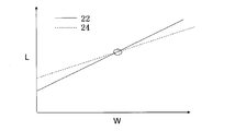
- Multimode to be satisfied in order for the TM polarization input from the second port on the input side provided at a position deviated from the first port to be distributed to the third port and the fourth port on the output side It is a graph which shows the curve showing the relationship between the length L and width W of an interference part.
- the multimode interference device 10 includes a multimode interference portion 12 formed of a silicon thin plate, a first port 14 formed at one end portion (first end portion 12 a) in the length direction of the multimode interference portion 12, and a first port 14.
- the second port 16 includes a third port 18 and a fourth port 20 formed at the other end portion (second end portion 12b) in the length direction of the multimode interference unit 12, and each port 14, 16, 18 , 20 is connected to an input / output waveguide (not shown) surrounded by, for example, SiO 2 (silicon dioxide).
- the distance between the first end 12a and the second end 12b of the multimode interference unit 12 is the length L
- the direction perpendicular to the length L is the width W
- the length direction is perpendicular to the width direction. This direction is referred to as thickness D.
- the first port 14 is provided at the center in the width direction of the first end portion 12a, that is, at a position on the inner side by W / 2 from the side end of the first end portion 12a toward the center in the width direction.
- the center is provided at a position on the inner side by W / 4 from either one of both side ends of the first end portion 12a toward the center in the width direction.
- the second port 16 is centered at a position on the inner side by W / 4 from the right end of the first end portion 12a toward the center in the width direction.
- the center may be provided at a position on the inner side by W / 4 from the left end of the first end portion 12a toward the center in the width direction.
- the TE polarized light is input to the first port 14, and the TE polarized light input to the first port 14 is output by being equally distributed to the third port 18 and the fourth port 20 with a loss of 3 dB. It has become. Also, TM polarized light is input to the second port 16, and the TM polarized light input to the second port 16 is evenly distributed and output to the third port 18 and the fourth port 20 with a loss of 3 dB. It is like that.
- the TE polarized light input to the first port 14 and the TM polarized light input to the second port 16 are both output to the third port 18 and the fourth port 20.
- the width W and the length L of the multimode interference part are determined so as to satisfy the following simultaneous equations (1).
- L c TE (W) is a function of the width W representing the coupling length of the multimode interference device with respect to TE polarized light
- L c TM (W) is the width W representing the coupling length of the multimode interference device with respect to TM polarization light. Is a function of
- the width W and the length L of the multimode interference unit 12 must satisfy the following expressions.
- the input from the first port 14 is performed.
- the two-branch output can be obtained from the third port 18 and the fourth port 20 for both the TE polarized light and the TM polarized light input from the second port 16.
- a curve 22 representing the relationship between L and W satisfying the equation (2) and a curve 24 representing the relationship between L and W satisfying the equation (3) produce an intersection, and the equation (2) and It was found that L and W simultaneously satisfying the formula (3) existed, and based on this, the formula (1) was obtained.
- FIG. 3 shows TE polarized light (FIG. 3A) and TM polarized light (FIG. 3) when the thickness D is 220 nm, the core width of the input / output waveguide is 450 nm, and the width W is 7.4 ⁇ m.
- the length L of the multimode interference section 12 is 153 ⁇ m. Also from the simulation results, it can be confirmed that the TE polarized light and the TM polarized light propagate to two common locations at a position separated by 153 ⁇ m from the input side end (first end 12a in FIG. 1).
- both the TE polarized light input to the first port 14 and the TM polarized light input to the second port 16 are the first. It can be seen that two branches from the third port 18 and the fourth port 20 are output evenly.
- the TM polarized light is also applied to the TE polarized light.
- a two-branch output can be obtained from the third port 18 and the fourth port 20 with a loss of 3 dB.
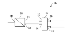
- FIG. 4 shows a polarization-independent 1 ⁇ 2 optical distributor 26 configured using the multimode interference device 10 shown in FIG.
- the 1 ⁇ 2 optical splitter 26 shown in FIG. 4 includes the multimode interference device 10 shown in FIG. 1 and a polarization separation element 28 provided in the front stage of the multimode interference device 10.
- the polarization separation element 28 has an input port 30, a TE polarization output port 32, and a TM polarization output port 34.
- the TE polarization output port 32 of the polarization separation element 28 is multimode interference by an optical waveguide.
- the TM polarization output port 34 of the polarization separation element 28 is connected to the first port 14 of the device 10 and is connected to the second port 16 of the multimode interference device 10 by an optical waveguide.
- polarization separation element 28 for example, a directional coupler can be used.
- the 1 ⁇ 2 optical distributor 26 having such a configuration, one input light is evenly distributed into two regardless of whether it is TE polarized light or TM polarized light, and polarization independent. Is done.
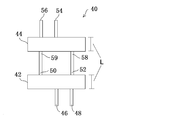
- FIG. 5 shows an element element 40 configured by using two multimode interference devices 42 and 44 as shown in FIG.
- the element element 40 shown in FIG. 5 has the same configuration as the multimode interference device 10 shown in FIG. 1 and has a first multimode interference device 42 and a second multimode arranged in tandem.
- An interference device 44 is provided.
- the first multimode interference device 42 has a first port 46 and a second port 48 provided at the first end, and a third port 50 and a fourth port 52 provided at the second end.
- the second multi-mode interference device 44 includes a first port 54 and a second port 56 provided at the first end, and a third port 58 and a fourth port 59 provided at the second end.
- the first multimode interference device 42 and the second multimode interference device 44 face each other on the second end side (the side on which the third ports 50 and 58 and the fourth ports 52 and 59 are provided).
- the third port 50 of the first multimode interference device 42 to the fourth port 59 of the second multimode interference device 44 and the fourth port 52 of the first multimode interference device 42 It is connected by an optical waveguide so as to be connected to the third port 58 of the second multimode interference device 44.
- the TE polarized light input from the first port 46 (the lower left port in FIG. 5) of the first multimode interference device 42 is the first port of the multimode interference device 44.
- the TM polarized light output from 54 (upper right port in FIG. 5) and input from the second port 48 (lower right port in FIG. 5) of the first multimode interference device 42 is second multimode interference.
- the cross function of the cross-polarization element 40 shown in FIG. 5 is the same as that of the cross-polarization element 40 ′ of the modified form shown in FIG. Even if the mode interference device 42 and the second multimode interference device 44 are connected and integrally formed, they can be maintained. Accordingly, the length L of the multimode interference device 10 shown in FIG. 1 is doubled, and the third port 18 is connected to the second end of the first end 12a opposite to the side near the second port 16. Side end of the end portion 12b (for example, in FIG.
- the second port 16 of the multimode interference device 10 is provided on the side close to the right end of the first end portion, so the left end of the second end portion)
- W / 4 is provided at the center side of the second end portion and the fourth port 20 is provided at the center of the second end portion, the cross polarization element 40 'shown in FIG. 6 is obtained.
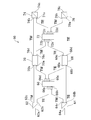
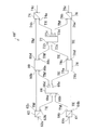
- FIG. 7 shows a 2 ⁇ 2 optical distributor (two-input two-output optical distributor) 60 that is made polarization independent by using the cross-polarization element 40 ′ shown in FIG. 5 or 6.
- the cross polarization element 40 ′ shown in FIG. 6 is used, but instead of the cross polarization element 40 ′, the cross polarization element 40 is used. Of course, it may be used.
- the 2 ⁇ 2 optical distributor 60 shown in FIG. 7 includes a first polarization separation element 62, a second polarization separation element 64, a first cross-polarization element 66 between different polarizations, and a TE polarization polarization element.
- the first polarization separation element 62 has an input port 62a, a TE polarization output port 62b, and a TM polarization output port 62c.
- the second polarization separation element 64 has an input port 64a, a TE polarization output port 64b, and a TM polarization output port 64c.
- any kind of polarization separation element may be used as long as the input light can be separated into TE polarization light and TM polarization light. Can do.
- the first polarization beam combiner 74 has a TE polarization input port 74a, a TM polarization input port 74b, and an output port 74c.
- the second polarization beam combining element 76 has a TE polarization input port 76a, a TM polarization input port 76b, and an output port 76c.
- any kind of polarization combining element can be used as long as it can synthesize and output TE polarized light and TM polarized light. Can be used.
- the 2 ⁇ 2 optical splitter 68 for TE polarization has two input ports 68a and 68b and two output ports 68c and 68d dedicated to TE polarization, and a 2 ⁇ 2 optical splitter 70 for TM polarization. Similarly, it has two input ports 70a and 70b dedicated to TM polarization and two output ports 70c and 70d.
- the TE polarization 2 ⁇ 2 optical distributor 68 and the TM polarization 2 ⁇ 2 optical distributor 70 have two input ports and two output ports, and are either TE polarized light or TM polarized light. Any type of 2 ⁇ 2 optical distributor can be used as long as light input to the two input ports can be evenly distributed to the two output ports.
- a 2 ⁇ 2 optical distributor 68 for TE polarization and a 2 ⁇ 2 optical distributor 70 for TM polarization a 2 ⁇ 2 MMI (multimode interference optical waveguide) dedicated to TE polarization or TM polarization is used. Can be used.
- the first cross polarization element 66 having different polarizations has an input side first port 66a, an input side second port 66b, an output side first port 66c, and an output side second port 66d.
- the wave crossing element 72 has an input side first port 72a and an input side second port 72b, an output side first port 72c, and an output side second port 72d.
- cross-polarization crossing elements 40 and 40 'as shown in FIG. 5 or 6 are used as the first cross-polarization crossing element 66 and the second cross-polarization crossing element 72.
- the TE polarization output port 62b of the first polarization separation element 62 is connected to the input side first port 66a of the first cross-polarization element 66 of the first different polarization by an optical waveguide.
- the TM polarization output port 62c is connected to one of the two input ports 70a and 70b of the 2 ⁇ 2 optical distributor 70 for TM polarization by an optical waveguide.
- the TE polarization output port 64b of the second polarization separation element 64 is connected to the input-side second port 66b of the first cross-polarization element 66 of the first different polarization by an optical waveguide, and the second polarization separation element
- the 64 TM polarization output ports 64c are connected to one of the two input ports 68a and 68b of the 2 ⁇ 2 optical distributor 68 for TE polarization by an optical waveguide.
- the output-side first port 66c of the first cross-polarization element 66 between the different polarizations is connected to the other input port 68a of the two input ports 68a and 68b of the 2 ⁇ 2 optical distributor 68 for TE polarization by an optical waveguide.
- the output-side second port 66d of the first cross-polarization element 66 having different polarizations is connected to the other 70a of the two input ports 70a and 70b of the 2 ⁇ 2 optical splitter 70 for TM polarization by an optical waveguide. .
- One of the two output ports 68c and 68d of the 2 ⁇ 2 optical distributor 68 for TE polarization is connected to the input side first port 72a of the second cross-polarization element 72 by the optical waveguide.
- the other 68d of the two output ports 68c and 68d of the 2 ⁇ 2 optical distributor 68 for polarization is connected to the TE polarization input port 76a of the second polarization beam combiner 76 by an optical waveguide.
- One of the two output ports 70c and 70d of the TM polarization 2 ⁇ 2 optical distributor 70c is connected to the input-side second port 72b of the second cross-polarization element 72 having different polarization by an optical waveguide.
- the other of the two output ports 70c and 70d of the 2 ⁇ 2 optical distributor 70 for TM polarization is connected to the TM polarization input port 74b of the first polarization beam combiner 74 by an optical waveguide.
- the output-side first port 72c of the second cross polarization element 72 with different polarizations is connected to the TE polarization input port 74a of the first polarization beam combining element by an optical waveguide, so
- the output second port 72d of 72 is connected to the TM polarization input port 76b of the second polarization beam combiner 76 by an optical waveguide.
- the two input lights are separated into the TE polarized light and the TM polarized light by the first polarization separation element 62 and the second polarization separation element 64, and the first different polarization is separated.
- two inputs for each polarized light are connected to 2 ⁇ 2 optical distributors 68 and 70 designed exclusively for each polarized light, and the 2 ⁇ 2 optical distributors 68 and 70 are connected.
- Is output again by the second cross-polarization crossing element 72, and the TE polarization and TM polarization are combined by the first polarization combining element 74 and the second polarization combining element 76. It becomes two output. Therefore, a polarization-independent 2 ⁇ 2 optical distributor 60 that functions without depending on the type of polarized light is realized.
- TM polarized wave having 2 ⁇ 2 optical switch 78 dedicated to TE polarization having input ports 78a and 78b and two output ports 78c and 78d, two input ports 80a and 80b, and two output ports 80c and 80d.
- the dedicated 2 ⁇ 2 optical switch 80 By using the dedicated 2 ⁇ 2 optical switch 80, a polarization-independent 2 ⁇ 2 optical switch 60 ′ that functions without depending on the type of polarization is realized. Since the operation is the same as that of the 2 ⁇ 2 optical distributor 60, it will not be described in detail here.
- the 2 ⁇ 2 optical switches 78 and 80 dedicated to TE polarization or TM polarization can be configured by, for example, two general 2 ⁇ 2 optical distributors and phase shifters.
- a polarization-independent element can be incorporated as an element in an optical node device such as an optical cross connect.
- the multimode interference device 10 according to the present invention and various devices or elements 26, 40, 40 ′, 60, 60 ′ using the multimode interference device 10 according to the present invention have been described with reference to the illustrated embodiments. It is not limited.
- the second port 16 is provided on the right side in the figure with respect to the first port 14, but is provided on the left side in the figure with respect to the first port 14. May be.
- Multimode interference device 12 Multimode interference part 12a 1st edge part 12b 2nd edge part 14 1st port 16 2nd port 18 3rd port 20 4th port 26 1x2 optical splitter 28 Polarization separation element 30 Input Port 32 TE Polarization Output Port 34 TM Polarization Output Port 40 Cross Polarization Cross Element 40 ′ Cross Polarization Cross Element 42 First Multimode Interference Device 44 Second Multimode Interference Device 46 First Port 48 First 2 port 50 3rd port 52 4th port 54 1st port 56 2nd port 58 3rd port 59 4th port 60 2x2 optical splitter 62 1st polarization separation element 62a Input port 62b TE polarization output port 62c TM polarization output port 64 second polarization separation element 64a input port 64b T Polarization output port 64c TM polarization output port 66 First cross polarization element 66a Input side first port 66b Input side second port 66c Output side first port 66d Out
Landscapes
- Physics & Mathematics (AREA)
- General Physics & Mathematics (AREA)
- Optics & Photonics (AREA)
- Optical Integrated Circuits (AREA)
- Optical Modulation, Optical Deflection, Nonlinear Optics, Optical Demodulation, Optical Logic Elements (AREA)
Description
本発明は、新規構造を持つ多モード干渉デバイスと、これを利用して、TE偏波光及びTM偏波光に依らずに使用できるように偏波無依存化した、1×2光分配器、異偏波間交差素子、2×2光分配器及び2×2光スイッチとに関する。
多モード干渉デバイスは、非特許文献1などに開示されているように、公知の技術であり、例えば、半導体光導波路に基づく1入力N出力の1×N光分配器又はN入力N出力のN×N光分配器や、N×Nスイッチなどを作製するときに用いられる。
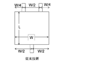
多モード干渉デバイスによって構成した標準的な1×2光分配器(1入力2出力の光分配器)及び2×2光分配器(2入力2出力の光分配器)がそれぞれ図9及び図10に示されている。図9に示されているように、1×2光分配器では、その幅をWとしたとき、入力ポートが入力側端部の中央(すなわち、W/2の位置)に設けられ、二つの出力ポートが出力側端部の両側端からそれぞれW/4だけ内側(中央に近づく側)の位置に設けられる。また、図10に示されているように、2×2光分配器では、その幅をWとしたとき、二つの入力ポートが入力側端部の両側端からそれぞれW/4だけ内側の位置に設けられ、二つの出力ポートが出力側端部の両側端からそれぞれW/4だけ内側の位置に設けられる。このような多モード干渉デバイスによって構成された2出力の光分配器は、多モード干渉部の長さL(すなわち、入力側端部と出力側端部との距離)を適切に選ぶことによって、二つの出力ポートに光が等分配される3dB光分配器となり、多モード干渉部の長さLは、近似的に、以下の式で与えられることが一般的に知られている。

ここで、kは非負の整数である。また、Lcは結合長と呼ばれ、β0をゼロ次モードの伝播定数、β1を1次モードの伝播係数としたときに、以下の式で定義される。

なお、β0、β1は何れも多モード干渉部の厚さ、幅W及び偏波の種類(TE偏波、TM偏波)に依存する定数である。すなわち、多モード干渉部の長さLは、多モード干渉部の厚さ、幅W及び偏波の種類に依存して変化する。
L.B. Soldano, E.C.M. Pennings,"Optical Multi-Mode Interference Devices Based on Self-Imaging: Principlesand Applications", J. Lightwave Technology, vol.13, no.4, pp.615-627(1995)
シリコン細線光導波路を用いた光回路は、大規模集積に向けた展望に明るいが、導波路コア断面の縦横比に由来して複屈折をもつことが多く、光回路の特性が偏波依存性を有する。すなわち、光回路の特性が、光回路を伝送される光がTE偏波であるかTM偏波であるかに依存する。しかしながら、光回路は、偏波の種類に依らずに用いることができるようにすることが望まれる。
例えば、従来の多モード干渉デバイスや、これを用いて構成された光分配器や光スイッチは、上述したように、多モード干渉部の長さLの選定に用いられる結合長Lcが偏波の種類に依存して変化するので、偏波依存性を有する。このため、多モード干渉デバイスや、多モード干渉デバイスを用いて構成された従来の光分配器や光スイッチは、TE偏波光専用又はTM偏波光専用に設計されており、TE偏波光にもTM偏波光にも利用できるようにすることが望まれる。しかしながら、従来の多モード干渉デバイスやこれを用いて構成された従来の光分配器又は光スイッチには、TE偏波光及びTM偏波光の両方に利用できるように偏波無依存化されたものは存在しなかった。
よって、本発明の目的は、従来技術に存する問題を解決して、光分配器、異偏波間交差素子及び光スイッチを偏波無依存化することができる多モード干渉デバイスを提供することにある。
上記目的に鑑み、本発明は、光伝送方向の両端に第一の端部と第二の端部とを有する幅Wの多モード干渉デバイスであって、前記第一の端部の幅方向中央に設けられた第一ポートと、前記第一の端部の幅方向の両端の何れか一方からW/4だけ内側に設けられた第二ポートと、前記第二の端部の幅方向の両端からそれぞれW/4だけ内側に設けられた第三ポート及び第四ポートとを備え、TE偏波光を前記第一ポートから入力したときに該TE偏波光を前記第三ポート及び前記第四ポートに均等に分配し且つTM偏波光を前記第二ポートから入力したときに該TM偏波光を前記第三ポート及び前記第四ポートに均等に分配するように前記光伝送方向の前記多モード干渉デバイスの長さLを定めた多モード干渉デバイスを提供する。
上記多モード干渉デバイスでは、TE偏波光を第一ポートに、TM偏波光を第二ポートに入力することによって、TE偏波光とTM偏波光の何れの場合でも、入力光を第三ポート及び第四ポートに均等に分配して出力することができる。
上記多モード干渉デバイスでは、TE偏波光に対する前記多モード干渉デバイスの結合長を表す幅Wの関数をLc
TE(W)、TM偏波光に対する前記多モード干渉デバイスの結合長を表す幅Wの関数をLc
TM(W)としたときに、以下の連立方程式を満たすL及びWをそれぞれ前記多モード干渉デバイスの長さ及び幅とすることが好ましい。

また、本発明は、入力ポートとTE偏波出力ポートとTM偏波出力ポートとを有し前記入力ポートに光を入力すると前記TE偏波出力ポートからTE偏波光を出力すると共に前記TM偏波出力ポートからTM偏波光を出力する偏波分離素子と、上記のような多モード干渉デバイスとを備え、前記偏波分離素子の前記TE偏波出力ポートを前記第一ポートに接続すると共に、前記偏波分離素子の前記TM偏波出力ポートを前記第二ポートに接続して、偏波無依存化した1×2光分配器を提供する。上記1×2光分配器では、偏波の種類に依らずに入力光が均等に配分されるので、偏波の種類に依存せずに使用することができる。
さらに、本発明は、上記のような多モード干渉デバイスを第二の端部同士が対向するように配置して、一方の多モード干渉デバイスの第三ポートと他方の多モード干渉デバイスの第四ポートとを接続すると共に、前記一方の多モード干渉デバイスの第四ポートを前記他方の多モード干渉デバイスの第三ポートとを接続し、前記一方の多モード干渉デバイスの第一ポートに入力されたTE偏波光が前記他方の多モード干渉デバイスの第一ポートから出力され、前記一方の多モード干渉デバイスの第二ポートに入力されたTM偏波光が前記他方の多モード干渉デバイスの第二ポートから出力されるようにした異偏波間交差素子を提供する。上記異偏波間交差素子では、第二の端部側が互いに対向して配置され、一方の多モード干渉デバイスの第三ポート及び第四ポートがそれぞれ他方の多モード干渉デバイスの第四ポート及び第三ポートに接続されているので、一方の多モード干渉デバイスの第二ポートと他方の多モード干渉デバイスの第二ポートの位置が第一ポートを挟んで反対側に配置される。したがって、第一ポートに入力されるTE偏波光と第二ポートに入力されるTM偏波光とが出力されるときに互いに対する相対位置が反転することになり、TE偏波光とTM偏波光を交差させる機能を奏する。
上記異偏波交差素子では、前記二つの多モード干渉デバイスを一体的に形成し、幅がW、長さが2Lとなるようにしてもよい。
また、本発明は、各々が入力ポートとTE偏波出力ポートとTM偏波出力ポートとを有する第一の偏波分離素子及び第二の偏波分離素子と、入力側第一ポート及び入力側第二ポートと出力側第一ポート及び出力側第二ポートとを有する上記の異偏波間交差素子のような第一の異偏波間交差素子と、各々が二つの入力ポートと二つの出力ポートを有するTE偏波用の2×2光分配器及びTM偏波用の2×2光分配器と、入力側第一ポート及び入力側第二ポートと出力側第一ポート及び出力側第二ポートとを有する上記の異偏波間交差素子のような第二の異偏波間交差素子と、各々がTE偏波入力ポートとTM偏波入力ポートと出力ポートとを有する第一の偏波合成素子及び第二の偏波合成素子とを順に備え、前記第一の偏波分離素子のTE偏波出力ポートを前記第一の異偏波間交差素子の前記入力側第一ポートに接続すると共に前記第二の偏波分離素子のTM偏波出力ポートを前記第一の異偏波間交差素子の前記入力側第二ポートに接続し、前記第一の偏波分離素子のTM偏波出力ポートと前記第一の異偏波間交差素子の出力側第二ポートとを前記TM偏波用の2×2光分配器の前記二つの入力ポートに接続すると共に、前記第二の偏波分離素子のTE偏波出力ポートと前記第一の異偏波交差素子の出力側第一ポートとを前記TE偏波用の2×2光分配器の前記二つの入力ポートに接続し、前記TM偏波用の2×2光分配器の前記二つの出力ポートの一方を前記第二の異偏波間交差素子の前記入力側第二ポートに接続すると共に、前記TE偏波用の2×2光分配器の前記二つの出力ポートの一方を前記第二の異偏波間交差素子の前記入力側第一ポートに接続し、前記TM偏波用の2×2光分配器の前記二つ出力ポートの他方と前記第二の異偏波間交差素子の前記出力側第一ポートとを前記第一の偏波合成素子の前記二つの入力ポートに接続すると共に、前記TE偏波用の2×2光分配器の前記二つの出力ポートの他方と前記第二の異偏波間交差素子の前記出力側第二ポートとを前記第二の偏波合成素子の前記二つの入力ポートに接続して、偏波無依存化した2×2光分配器を提供する。
また、本発明は、各々が入力ポートとTE偏波出力ポートとTM偏波出力ポートとを有する第一の偏波分離素子及び第二の偏波分離素子と、入力側第一ポート及び入力側第二ポートと出力側第一ポート及び出力側第二ポートとを有する上記の異偏波交差素子のような第一の異偏波間交差素子と、各々が二つの入力ポートと二つの出力ポートを有するTE偏波用の2×2光スイッチ及びTM偏波用の2×2光スイッチと、入力側第一ポート及び入力側第二ポートと出力側第一ポート及び出力側第二ポートとを有する上記の異偏波交差素子のような第二の異偏波間交差素子と、各々がTE偏波入力ポートとTM偏波入力ポートと出力ポートとを有する第一の偏波合成素子及び第二の偏波合成素子とを順に備え、前記第一の偏波分離素子のTE偏波出力ポートを前記第一の異偏波間交差素子の前記入力側第一ポートに接続すると共に前記第二の偏波分離素子のTM偏波出力ポートを前記第一の異偏波間交差素子の前記入力側第二ポートに接続し、前記第一の偏波分離素子のTM偏波出力ポートと前記第一の異偏波間交差素子の出力側第二ポートとを前記TM偏波用の2×2光スイッチの前記二つの入力ポートに接続すると共に、前記第二の偏波分離素子のTE偏波出力ポートと前記第一の異偏波交差素子の出力側第一ポートとを前記TE偏波用の2×2光スイッチの前記二つの入力ポートに接続し、前記TM偏波用の2×2光スイッチの前記二つの出力ポートの一方を前記第二の異偏波間交差素子の前記入力側第二ポートに接続すると共に、前記TE偏波用の2×2光スイッチの前記二つの出力ポートの一方を前記第二の異偏波間交差素子の前記入力側第一ポートに接続し、前記TM偏波用の2×2光スイッチの前記二つの出力ポートの他方と前記第二の異偏波間交差素子の前記出力側第一ポートとを前記第一の偏波合成素子の前記二つの入力ポートに接続すると共に、前記TE偏波用の2×2光スイッチの前記二つの出力ポートの他方と前記第二の異偏波間交差素子の前記出力側第二ポートとを前記第二の偏波合成素子の前記二つの入力ポートに接続して、偏波無依存化した2×2光スイッチを提供する。
本発明の多モード干渉デバイスによれば、TE偏波光専用の入力ポート及びTM偏波光専用の入力ポートが設けられ、入力光がTE偏波光の場合でも、TM偏波光の場合でも入力光を二つのポートに均等に配分することができるようになる。また、上記多モード干渉デバイスを用いれば、1×2光分配器を偏波無依存化することができる。さらに、上記多モード干渉デバイスを用いればTE偏波光とTM偏波光とを交差させる機能を果たす異偏波間交差素子を提供することができ、これを用いることによって偏波無依存化された2×2光分配器及び2×2光スイッチが提供される。このような偏波無依存化された1×2光分配器、2×2光分配器及び2×2光スイッチは、光クロスコネクトなど光ノード装置に要素素子として組み込まれる素子として特に有用となる。
以下、図面を参照して、本発明による多モード干渉デバイスの実施の形態を説明する。
最初に、図1を参照して、本発明による多モード干渉デバイス10の全体構成を説明する。多モード干渉デバイス10は、シリコン薄板によって形成された多モード干渉部12と、多モード干渉部12の長さ方向の一端部(第一の端部12a)に形成された第一ポート14及び第二ポート16と、多モード干渉部12の長さ方向の他端部(第二の端部12b)に形成された第三ポート18及び第四ポート20とを備え、各ポート14,16,18,20には、例えばSiO2(二酸化ケイ素)で周囲を囲まれた入出力導波路(図示せず)が接続される。以下では、多モード干渉部12の第一の端部12aと第二の端部12bの間の距離を長さL、長さLと垂直な方向を幅W、長さ方向と幅方向に垂直な方向を厚さDと記載する。
第一ポート14は、第一の端部12aの幅方向の中央、すなわち第一の端部12aの側端から幅方向中央へ向かってW/2だけ内側の位置に設けられ、第二ポート16は、第一の端部12aの側端の両側端の何れか一方から幅方向中央へ向かってW/4だけ内側の位置に中心が設けられる。図1では、第二ポート16は、第一の端部12aの右側端から幅方向中央へ向かってW/4だけ内側の位置に中心が設けられているが、図1に破線で描かれているように、第一の端部12aの左側端から幅方向中央へ向かってW/4だけ内側の位置に中心が設けられていてもよい。
第一ポート14にはTE偏波光が入力され、第一ポート14に入力されたTE偏波光は、3dBの損失で第三ポート18及び第四ポート20に均等に配分されて出力されるようになっている。また、第二ポート16にはTM偏波光が入力され、第二ポート16に入力されたTM偏波光は、3dBの損失で第三ポート18及び第四ポート20に均等に配分されて出力されるようになっている。
多モード干渉デバイス10では、第一ポート14に入力されたTE偏波光及び第二ポート16に入力されたTM偏波光が共に第三ポート18及び第四ポート20に出力されるようにするために、多モード干渉部の幅W及び長さLが以下の連立方程式(1)を満たすように定められる。

ここで、Lc
TE(W)はTE偏波光に対する多モード干渉デバイスの結合長を表す幅Wの関数、Lc
TM(W)はTM偏波光に対する多モード干渉デバイスの結合長を表す幅Wの関数である。
上記式は以下のようにして求められる。
第一ポート14に入力された光が第三ポート18及び第四ポート20に分配されて出力されるためには、結合長を表す関数をLc(W)としたとき、1×2分配器の場合と同様に、多モード干渉部12の幅W及び長さLは以下の式を満たさなくてはならない。

第一ポート14に入力された光が第三ポート18及び第四ポート20に分配されて出力されるためには、結合長を表す関数をLc(W)としたとき、1×2分配器の場合と同様に、多モード干渉部12の幅W及び長さLは以下の式を満たさなくてはならない。
また、第二ポート16に入力された光が第三ポート18及び第四ポート20に分配されて出力されるためには、結合長を表す関数をLc(W)としたとき、2×2分配器の場合と同様に、多モード干渉部12の幅W及び長さLは以下の式を満たさなくてはならない。

よって、式(2)によって表される曲線と式(3)によって表される曲線の交点に対応する幅W及び長さLをそれぞれ多モード干渉部の寸法とすれば、第一ポート14から入力されるTE偏波光に対しても、第二ポート16から入力されるTM偏波光に対しても、第三ポート18及び第四ポート20から2分岐出力が得られるようになる。
本願発明者は、第一ポート14にTE偏波光を入力すると共に第二ポート16にTM偏波光を入力し、式(2)においてk=1、式(3)においてk=0としたときに、図4に示すように、式(2)を満たすLとWの関係を表す曲線22と式(3)を満たすLとWの関係を表す曲線24とが交点を生じ、式(2)及び式(3)を同時に満たすL及びWが存在することを見出し、これに基づいて、式(1)を得た。
実例として、図3は、厚さDが220nm、入出力導波路のコアの幅が450nm、幅Wが7.4μmとしたときのTE偏波光(図3(a))及びTM偏波光(図3(b))の伝播状態を有限差分時間領域法によって2次元演算したときのシミュレーション結果を示している。同条件で連立方程式(1)を解くと、多モード干渉部12の長さLは153μmとなる。シミュレーション結果からも、入力側端部(図1における第一の端部12a)から153μmだけ離れた位置において、TE偏波光及びTM偏波光が二つの共通する箇所に伝播していることが確認できる。したがって、これら二つの共通する箇所に第三ポート18及び第四ポート20を設ければ、第一ポート14に入力されたTE偏波光及び第二ポート16に入力されたTM偏波光の両方が第三ポート18及び第四ポート20から2分岐されて均等に出力されるようになることが分かる。
このように、本発明の多モード干渉デバイス10では、TE偏波光を第一ポート14に入力し、TM偏波光を第二ポート16に入力すれば、TE偏波光に対しても、TM偏波光に対しても、第三ポート18及び第四ポート20から3dBの損失で2分岐出力が得られる。
このような本発明による多モード干渉デバイス10を用いることにより、偏波無依存化された様々な要素素子を構成することができる。以下に、図4から図8を参照して、本発明による多モード干渉デバイス10を用いて構成される様々な偏波無依存の要素素子を説明する。
図4は、図1に示されている多モード干渉デバイス10を用いて構成された偏波無依存の1×2光分配器26を示している。図4に示されている1×2光分配器26は、図1に示されている多モード干渉デバイス10と、多モード干渉デバイス10の前段に設けられた偏波分離素子28とを備える。偏波分離素子28は、入力ポート30と、TE偏波出力ポート32と、TM偏波出力ポート34とを有し、偏波分離素子28のTE偏波出力ポート32は光導波路により多モード干渉デバイス10の第一ポート14に接続され、偏波分離素子28のTM偏波出力ポート34は光導波路により多モード干渉デバイス10の第二ポート16に接続されている。偏波分離素子28としては、例えば方向性結合器を用いることができる。このような構成の1×2光分配器26によれば、一つの入力光がTE偏波光かTM偏波光かに依らずに二つに均等に分配されるようになり、偏波無依存化される。
図5は、図1に示されているような多モード干渉デバイス42,44を二つ用いて構成された要素素子40である。図5に示されている要素素子40は、図1に示されている多モード干渉デバイス10と同様の構成を有し縦列に配置された第一の多モード干渉デバイス42及び第二の多モード干渉デバイス44を備える。第一の多モード干渉デバイス42は第一の端部に設けられた第一ポート46及び第二ポート48と第二の端部に設けられた第三ポート50及び第四ポート52とを有し、同様に、第二の多モード干渉デバイス44も第一の端部に設けた第一ポート54及び第二ポート56と第二の端部に設けられた第三ポート58及び第四ポート59とを有する。第一の多モード干渉デバイス42と第二の多モード干渉デバイス44とは、第二の端部側(第三ポート50,58及び第四ポート52,59が設けられている側)を互いに対向させて配置され、第一の多モード干渉デバイス42の第三ポート50を第二の多モード干渉デバイス44の第四ポート59に接続し且つ第一の多モード干渉デバイス42の第四ポート52を第二の多モード干渉デバイス44の第三ポート58に接続するように、光導波路によって接続されている。
このように構成された要素素子40では、第一の多モード干渉デバイス42の第一ポート46(図5における下方左側のポート)から入力されたTE偏波光は多モード干渉デバイス44の第一ポート54(図5における上方右側のポート)から出力され、第一の多モード干渉デバイス42の第二ポート48(図5における下方右側のポート)から入力されたTM偏波光は第二の多モード干渉デバイス44の第二ポート56(図5における上方左側のポート)から出力される。すなわち、図5に示されている要素素子は、幅方向におけるTE偏波光とTM偏波光の並び順を入れ替えて出力し、TE偏波光とTM偏波光とを交差させる異偏波間交差素子40として機能する。
図5に示されている異偏波間交差素子40の交差機能は、図6に示されている変形形態の異偏波交差素子40´のように、光導波路を用いずに、第一の多モード干渉デバイス42と第二の多モード干渉デバイス44との間を接続し、一体的に形成しても、維持することができる。したがって、図1に示されている多モード干渉デバイス10の長さLを2倍にし、第三ポート18を第一の端部12aの第二ポート16に近い側端と反対側の第二の端部12bの側端(例えば図1では、多モード干渉デバイス10の第二ポート16が第一の端部の右側端に近い側に設けられているので、第二の端部の左側端)からW/4だけ第二の端部の中央側に設け、第四ポート20を第二の端部の中央に設ければ、図6に示されている異偏波間交差素子40´となる。
また、図5又は図6に示されている異偏波間交差素子40又は40´のTE偏波光とTM偏波光とを交差させる機能を利用すれば、2×2光分配器や2×2光スイッチの偏波無依存化を図ることが可能となる。
図7は、図5又は図6に示されている異偏波間交差素子40´を用いて偏波無依存化した2×2光分配器(2入力2出力の光分配器)60を示す。図7に示されている実施形態では、図6に示されている異偏波間交差素子40´が使用されているが、異偏波間交差素子40´に代えて、異偏波間交差素子40を使用してもよいことはもちろんである。
図7に示されている2×2光分配器60は、第一の偏波分離素子62及第二の偏波分離素子64と、第一の異偏波間交差素子66と、TE偏波用の2×2光分配器68及びTM偏波用の2×2光分配器70と、第二の異偏波間交差素子72と、第一の偏波合成素子74及び第二の偏波合成素子76とを順に備える。
第一の偏波分離素子62は、入力ポート62aとTE偏波出力ポート62bとTM偏波出力ポート62cとを有する。同様に、第二の偏波分離素子64は、入力ポート64aとTE偏波出力ポート64bとTM偏波出力ポート64cとを有する。第一の偏波分離素子62及び第二の偏波分離素子64としては、入力光をTE偏波光とTM偏波光とに分離できるものであれば任意の種類の偏波分離素子を使用することができる。
第一の偏波合成素子74は、TE偏波入力ポート74aとTM偏波入力ポート74bと出力ポート74cとを有する。同様に、第二の偏波合成素子76は、TE偏波入力ポート76aとTM偏波入力ポート76bと出力ポート76cとを有する。第一の偏波合成素子74及び第二の偏波合成素子76としては、TE偏波光とTM偏波光とを合成して出力することができるものであれば、任意の種類の偏波合成素子を使用することができる。
TE偏波用の2×2光分配器68はTE偏波専用の二つの入力ポート68a,68bと二つの出力ポート68c,68dとを有し、TM偏波用の2×2光分配器70も同様にTM偏波専用の二つの入力ポート70a,70bと二つの出力ポート70c,70dとを有する。TE偏波用の2×2光分配器68及びTM偏波用2×2光分配器70としては、二つの入力ポートと二つの出力ポートとを有し且つTE偏波光又はTM偏波光の何れか一方のみについて二つの入力ポートに入力された光を二つの出力ポートに均等に分配できれば任意の種類の2×2光分配器を使用することができる。例えば、TE偏波用の2×2光分配器68及びTM偏波用の2×2光分配器70として、TE偏波専用又はTM偏波専用の2×2MMI(多モード干渉光導波路)を使用することができる。
第一の異偏波間交差素子66は入力側第一ポート66a及び入力側第二ポート66bと出力側第一ポート66c及び出力側第二ポート66dとを有し、同様に、第二の異偏波間交差素子72は入力側第一ポート72a及び入力側第二ポート72bと出力側第一ポート72c及び出力側第二ポート72dとを有する。第一の異偏波間交差素子66及び第二の異偏波間交差素子72としては、図5又は図6に示されているような異偏波間交差素子40,40´が使用される。
第一の偏波分離素子62のTE偏波出力ポート62bは、光導波路によって、第一の異偏波間交差素子66の入力側第一ポート66aに接続され、第一の偏波分離素子62のTM偏波出力ポート62cは、光導波路によって、TM偏波用の2×2光分配器70の二つの入力ポート70a,70bの一方70bに接続される。また、第二の偏波分離素子64のTE偏波出力ポート64bは、光導波路によって、第一の異偏波間交差素子66の入力側第二ポート66bに接続され、第二の偏波分離素子64のTM偏波出力ポート64cは、光導波路によって、TE偏波用の2×2光分配器68の二つの入力ポート68a,68bの一方68bに接続される。さらに、第一の異偏波間交差素子66の出力側第一ポート66cは、光導波路によって、TE偏波用の2×2光分配器68の二つの入力ポート68a,68bの他方68aに接続され、第一の異偏波間交差素子66の出力側第二ポート66dは、光導波路によって、TM偏波用の2×2光分配器70の二つの入力ポート70a,70bの他方70aに接続される。
TE偏波用の2×2光分配器68の二つの出力ポート68c,68dの一方68cは、光導波路によって、第二の異偏波間交差素子72の入力側第一ポート72aに接続され、TE偏波用の2×2光分配器68の二つの出力ポート68c,68dの他方68dは、光導波路によって、第二の偏波合成素子76のTE偏波入力ポート76aに接続される。また、TM偏波用の2×2光分配器70の二つの出力ポート70c,70dの一方70cは、光導波路によって、第二の異偏波間交差素子72の入力側第二ポート72bに接続され、TM偏波用の2×2光分配器70の二つの出力ポート70c,70dの他方70dは、光導波路によって、第一の偏波合成素子74のTM偏波入力ポート74bに接続される。さらに、第二の異偏波間交差素子72の出力側第一ポート72cは、光導波路によって、第一の偏波合成素子のTE偏波入力ポート74aに接続され、第二の異偏波間交差素子72の出力側第二ポート72dは、光導波路によって、第二の偏波合成素子76のTM偏波入力ポート76bに接続される。
このような構成にすることにより、二つの入力光が第一の偏波分離素子62及び第二の偏波分離素子64によってTE偏波光とTM偏波光とに分離されて第一の異偏波間交差素子66によって位置を入れ替えられた後、偏波光ごとの2入力がそれぞれの偏波光専用に設計された2×2光分配器68,70に接続されて、2×2光分配器68,70の出力が第二の異偏波間交差素子72によって再び位置を入れ替えられ、さらに、第一の偏波合成素子74及び第二の偏波合成素子76によってTE偏波とTM偏波が合成して二つの出力とされるようになる。したがって、偏波光の種類に依存せずに機能する偏波無依存の2×2光分配器60が実現される。
同様に、図8に示されているように、図7のTE偏波専用の2×2光分配器68とTM偏波専用の2×2光分配器70とに代えて、それぞれ、二つの入力ポート78a,78bと二つの出力ポート78c,78dとを有するTE偏波専用の2×2光スイッチ78と、二つの入力ポート80a,80bと二つの出力ポート80c,80dとを有するTM偏波専用の2×2光スイッチ80とを用いることによって、偏波の種類に依存せずに機能する偏波無依存の2×2光スイッチ60´が実現される。その動作は、2×2光分配器60と同様であるので、ここでは詳しく説明しない。なお、TE偏波専用又はTM偏波専用の2×2光スイッチ78,80は、例えば二つの一般的な2×2光分配器と位相シフタによって構成することができることは公知である。
このように本発明による多モード干渉デバイス10を用いれば、1×2光分配器26、異偏波間交差素子40,40´、2×2光分配器60、2×2光スイッチ60´などを偏波無依存化することができる。このような偏波無依存化された素子は、光クロスコネクトなど光ノード装置に要素素子として組み込むことができる。
以上、図示される実施形態を参照して、本発明による多モード干渉デバイス10及びこれを用いた各種デバイス又は素子26,40,40´,60,60´を説明したが、本発明はこれらに限定されるものではない。例えば、図1に示されている多モード干渉デバイス10では、第二ポート16が第一ポート14に対して図中右側に設けられているが、第一ポート14に対して図中左側に設けられてもよい。
10 多モード干渉デバイス
12 多モード干渉部
12a 第一の端部
12b 第二の端部
14 第一ポート
16 第二ポート
18 第三ポート
20 第四ポート
26 1×2光分配器
28 偏波分離素子
30 入力ポート
32 TE偏波出力ポート
34 TM偏波出力ポート
40 異偏波間交差素子
40´ 異偏波間交差素子
42 第一の多モード干渉デバイス
44 第二の多モード干渉デバイス
46 第一ポート
48 第二ポート
50 第三ポート
52 第四ポート
54 第一ポート
56 第二ポート
58 第三ポート
59 第四ポート
60 2×2光分配器
62 第一の偏波分離素子
62a 入力ポート
62b TE偏波出力ポート
62c TM偏波出力ポート
64 第二の偏波分離素子
64a 入力ポート
64b TE偏波出力ポート
64c TM偏波出力ポート
66 第一の異偏波間交差素子
66a 入力側第一ポート
66b 入力側第二ポート
66c 出力側第一ポート
66d 出力側第二ポート
68 2×2光分配器
68a,68b 入力ポート
68c,68d 出力ポート
70 2×2光分配器
70a,70b 入力ポート
70c,70d 出力ポート
72 第二の異偏波間交差素子
72a 入力側第一ポート
72b 入力側第二ポート
72c 出力側第一ポート
72d 出力側第二ポート
74 第一の偏波合成素子
74a TE偏波入力ポート
74b TM偏波入力ポート
74c 出力ポート
76 第二の偏波合成素子
76a TE偏波入力ポート
76b TM偏波入力ポート
76c 出力ポート
78 2×2光スイッチ
78a,78b 入力ポート
78c,78d 出力ポート
80 2×2光スイッチ
80a,80b 入力ポート
80c,80d 出力ポート
12 多モード干渉部
12a 第一の端部
12b 第二の端部
14 第一ポート
16 第二ポート
18 第三ポート
20 第四ポート
26 1×2光分配器
28 偏波分離素子
30 入力ポート
32 TE偏波出力ポート
34 TM偏波出力ポート
40 異偏波間交差素子
40´ 異偏波間交差素子
42 第一の多モード干渉デバイス
44 第二の多モード干渉デバイス
46 第一ポート
48 第二ポート
50 第三ポート
52 第四ポート
54 第一ポート
56 第二ポート
58 第三ポート
59 第四ポート
60 2×2光分配器
62 第一の偏波分離素子
62a 入力ポート
62b TE偏波出力ポート
62c TM偏波出力ポート
64 第二の偏波分離素子
64a 入力ポート
64b TE偏波出力ポート
64c TM偏波出力ポート
66 第一の異偏波間交差素子
66a 入力側第一ポート
66b 入力側第二ポート
66c 出力側第一ポート
66d 出力側第二ポート
68 2×2光分配器
68a,68b 入力ポート
68c,68d 出力ポート
70 2×2光分配器
70a,70b 入力ポート
70c,70d 出力ポート
72 第二の異偏波間交差素子
72a 入力側第一ポート
72b 入力側第二ポート
72c 出力側第一ポート
72d 出力側第二ポート
74 第一の偏波合成素子
74a TE偏波入力ポート
74b TM偏波入力ポート
74c 出力ポート
76 第二の偏波合成素子
76a TE偏波入力ポート
76b TM偏波入力ポート
76c 出力ポート
78 2×2光スイッチ
78a,78b 入力ポート
78c,78d 出力ポート
80 2×2光スイッチ
80a,80b 入力ポート
80c,80d 出力ポート
Claims (9)
- 光伝送方向の両端に第一の端部と第二の端部とを有する幅Wの多モード干渉デバイスであって、
前記第一の端部の幅方向中央に設けられた第一ポートと、前記第一の端部の幅方向の両端の何れか一方からW/4だけ内側に設けられた第二ポートと、前記第二の端部の幅方向の両端からそれぞれW/4だけ内側に設けられた第三ポート及び第四ポートとを備え、TE偏波光を前記第一ポートから入力したときに該TE偏波光を前記第三ポート及び前記第四ポートに均等に分配し且つTM偏波光を前記第二ポートから入力したときに該TM偏波光を前記第三ポート及び前記第四ポートに均等に分配するように前記光伝送方向の前記多モード干渉デバイスの長さLを定めたことを特徴とする多モード干渉デバイス。 - TE偏波光に対する前記多モード干渉デバイスの結合長を表す幅Wの関数をLc TE(W)、TM偏波光に対する前記多モード干渉デバイスの結合長を表す幅Wの関数をLc TM(W)としたときに、以下の連立方程式を満たすL及びWをそれぞれ前記多モード干渉デバイスの長さ及び幅とした、請求項1に記載の多モード干渉デバイス。

- 入力ポートとTE偏波出力ポートとTM偏波出力ポートとを有し入力ポートに光を入力すると前記TE偏波出力ポートからTE偏波光を出力すると共に前記TM偏波出力ポートからTM偏波光を出力する偏波分離素子と、請求項1又は請求項2に記載の多モード干渉デバイスとを備え、前記偏波分離素子の前記TE偏波出力ポートを前記第一ポートに接続すると共に、前記偏波分離素子の前記TM偏波出力ポートを前記第二ポートに接続して、偏波無依存化したことを特徴とする1×2光分配器。
- 二つの請求項1又は請求項2に記載の多モード干渉デバイスを第二の端部同士が対向するように配置して、一方の多モード干渉デバイスの第三ポートと他方の多モード干渉デバイスの第四ポートとを接続すると共に、前記一方の多モード干渉デバイスの第四ポートを前記他方の多モード干渉デバイスの第三ポートとを接続し、前記一方の多モード干渉デバイスの第一ポートに入力されたTE偏波光が前記他方の多モード干渉デバイスの第一ポートから出力され、前記一方の多モード干渉デバイスの第二ポートに入力されたTM偏波光が前記他方の多モード干渉デバイスの第二ポートから出力されるようにしたことを特徴とする異偏波間交差素子。
- 前記二つの多モード干渉デバイスを一体的に形成し、幅がW、長さが2Lとなるようにした、請求項4に記載の異偏波間交差素子。
- 各々が入力ポートとTE偏波出力ポートとTM偏波出力ポートとを有する第一の偏波分離素子及び第二の偏波分離素子と、入力側第一ポート及び入力側第二ポートと出力側第一ポート及び出力側第二ポートとを有する請求項4に記載の第一の異偏波間交差素子と、各々が二つの入力ポートと二つの出力ポートを有するTE偏波用の2×2光分配器及びTM偏波用の2×2光分配器と、入力側第一ポート及び入力側第二ポートと出力側第一ポート及び出力側第二ポートとを有する請求項4に記載の第二の異偏波間交差素子と、各々がTE偏波入力ポートとTM偏波入力ポートと出力ポートとを有する第一の偏波合成素子及び第二の偏波合成素子とを順に備え、
前記第一の偏波分離素子のTE偏波出力ポートを前記第一の異偏波間交差素子の前記入力側第一ポートに接続すると共に前記第二の偏波分離素子のTM偏波出力ポートを前記第一の異偏波間交差素子の前記入力側第二ポートに接続し、
前記第一の偏波分離素子のTM偏波出力ポートと前記第一の異偏波間交差素子の出力側第二ポートとを前記TM偏波用の2×2光分配器の前記二つの入力ポートに接続すると共に、前記第二の偏波分離素子のTE偏波出力ポートと前記第一の異偏波交差素子の出力側第一ポートとを前記TE偏波用の2×2光分配器の前記二つの入力ポートに接続し、
前記TM偏波用の2×2光分配器の前記二つの出力ポートの一方を前記第二の異偏波間交差素子の前記入力側第二ポートに接続すると共に、前記TE偏波用の2×2光分配器の前記二つの出力ポートの一方を前記第二の異偏波間交差素子の前記入力側第一ポートに接続し、
前記TM偏波用の2×2光分配器の前記二つ出力ポートの他方と前記第二の異偏波間交差素子の前記出力側第一ポートとを前記第一の偏波合成素子の前記二つの入力ポートに接続すると共に、前記TE偏波用の2×2光分配器の前記二つの出力ポートの他方と前記第二の異偏波間交差素子の前記出力側第二ポートとを前記第二の偏波合成素子の前記二つの入力ポートに接続して、偏波無依存化したことを特徴とする2×2光分配器。 - 各々が入力ポートとTE偏波出力ポートとTM偏波出力ポートとを有する第一の偏波分離素子及び第二の偏波分離素子と、入力側第一ポート及び入力側第二ポートと出力側第一ポート及び出力側第二ポートとを有する請求項5に記載の第一の異偏波間交差素子と、各々が二つの入力ポートと二つの出力ポートを有するTE偏波用の2×2光分配器及びTM偏波用の2×2光分配器と、入力側第一ポート及び入力側第二ポートと出力側第一ポート及び出力側第二ポートとを有する請求項5に記載の第二の異偏波間交差素子と、各々がTE偏波入力ポートとTM偏波入力ポートと出力ポートとを有する第一の偏波合成素子及び第二の偏波合成素子とを順に備え、
前記第一の偏波分離素子のTE偏波出力ポートを前記第一の異偏波間交差素子の前記入力側第一ポートに接続すると共に前記第二の偏波分離素子のTM偏波出力ポートを前記第一の異偏波間交差素子の前記入力側第二ポートに接続し、
前記第一の偏波分離素子のTM偏波出力ポートと前記第一の異偏波間交差素子の出力側第二ポートとを前記TM偏波用の2×2光分配器の前記二つの入力ポートに接続すると共に、前記第二の偏波分離素子のTE偏波出力ポートと前記第一の異偏波交差素子の出力側第一ポートとを前記TE偏波用の2×2光分配器の前記二つの入力ポートに接続し、
前記TM偏波用の2×2光分配器の前記二つの出力ポートの一方を前記第二の異偏波間交差素子の前記入力側第二ポートに接続すると共に、前記TE偏波用の2×2光分配器の前記二つの出力ポートの一方を前記第二の異偏波間交差素子の前記入力側第一ポートに接続し、
前記TM偏波用の2×2光分配器の前記二つ出力ポートの他方と前記第二の異偏波間交差素子の前記出力側第一ポートとを前記第一の偏波合成素子の前記二つの入力ポートに接続すると共に、前記TE偏波用の2×2光分配器の前記二つの出力ポートの他方と前記第二の異偏波間交差素子の前記出力側第二ポートとを前記第二の偏波合成素子の前記二つの入力ポートに接続して、偏波無依存化したことを特徴とする2×2光分配器。 - 各々が入力ポートとTE偏波出力ポートとTM偏波出力ポートとを有する第一の偏波分離素子及び第二の偏波分離素子と、入力側第一ポート及び入力側第二ポートと出力側第一ポート及び出力側第二ポートとを有する請求項4に記載の第一の異偏波間交差素子と、各々が二つの入力ポートと二つの出力ポートを有するTE偏波用の2×2光スイッチ及びTM偏波用の2×2光スイッチと、入力側第一ポート及び入力側第二ポートと出力側第一ポート及び出力側第二ポートとを有する請求項4に記載の第二の異偏波間交差素子と、各々がTE偏波入力ポートとTM偏波入力ポートと出力ポートとを有する第一の偏波合成素子及び第二の偏波合成素子とを順に備え、
前記第一の偏波分離素子のTE偏波出力ポートを前記第一の異偏波間交差素子の前記入力側第一ポートに接続すると共に前記第二の偏波分離素子のTM偏波出力ポートを前記第一の異偏波間交差素子の前記入力側第二ポートに接続し、
前記第一の偏波分離素子のTM偏波出力ポートと前記第一の異偏波間交差素子の出力側第二ポートとを前記TM偏波用の2×2光スイッチの前記二つの入力ポートに接続すると共に、前記第二の偏波分離素子のTE偏波出力ポートと前記第一の異偏波交差素子の出力側第一ポートとを前記TE偏波用の2×2光スイッチの前記二つの入力ポートに接続し、
前記TM偏波用の2×2光スイッチの前記二つの出力ポートの一方を前記第二の異偏波間交差素子の前記入力側第二ポートに接続すると共に、前記TE偏波用の2×2光スイッチの前記二つの出力ポートの一方を前記第二の異偏波間交差素子の前記入力側第一ポートに接続し、
前記TM偏波用の2×2光スイッチの前記二つの出力ポートの他方と前記第二の異偏波間交差素子の前記出力側第一ポートとを前記第一の偏波合成素子の前記二つの入力ポートに接続すると共に、前記TE偏波用の2×2光スイッチの前記二つの出力ポートの他方と前記第二の異偏波間交差素子の前記出力側第二ポートとを前記第二の偏波合成素子の前記二つの入力ポートに接続して、偏波無依存化したことを特徴とする2×2光スイッチ。 - 各々が入力ポートとTE偏波出力ポートとTM偏波出力ポートとを有する第一の偏波分離素子及び第二の偏波分離素子と、入力側第一ポート及び入力側第二ポートと出力側第一ポート及び出力側第二ポートとを有する請求項5に記載の第一の異偏波間交差素子と、各々が二つの入力ポートと二つの出力ポートを有するTE偏波用の2×2光スイッチ及びTM偏波用の2×2光スイッチと、入力側第一ポート及び入力側第二ポートと出力側第一ポート及び出力側第二ポートとを有する請求項5に記載の第二の異偏波間交差素子と、各々がTE偏波入力ポートとTM偏波入力ポートと出力ポートとを有する第一の偏波合成素子及び第二の偏波合成素子とを順に備え、
前記第一の偏波分離素子のTE偏波出力ポートを前記第一の異偏波間交差素子の前記入力側第一ポートに接続すると共に前記第二の偏波分離素子のTM偏波出力ポートを前記第一の異偏波間交差素子の前記入力側第二ポートに接続し、
前記第一の偏波分離素子のTM偏波出力ポートと前記第一の異偏波間交差素子の出力側第二ポートとを前記TM偏波用の2×2光スイッチの前記二つの入力ポートに接続すると共に、前記第二の偏波分離素子のTE偏波出力ポートと前記第一の異偏波交差素子の出力側第一ポートとを前記TE偏波用の2×2光スイッチの前記二つの入力ポートに接続し、
前記TM偏波用の2×2光スイッチの前記二つの出力ポートの一方を前記第二の異偏波間交差素子の前記入力側第二ポートに接続すると共に、前記TE偏波用の2×2光スイッチの前記二つの出力ポートの一方を前記第二の異偏波間交差素子の前記入力側第一ポートに接続し、
前記TM偏波用の2×2光スイッチの前記二つの出力ポートの他方と前記第二の異偏波間交差素子の前記出力側第一ポートとを前記第一の偏波合成素子の前記二つの入力ポートに接続すると共に、前記TE偏波用の2×2光スイッチの前記二つの出力ポートの他方と前記第二の異偏波間交差素子の前記出力側第二ポートとを前記第二の偏波合成素子の前記二つの入力ポートに接続して、偏波無依存化したことを特徴とする2×2光スイッチ。
Priority Applications (1)
| Application Number | Priority Date | Filing Date | Title |
|---|---|---|---|
| PCT/JP2012/070650 WO2014027397A1 (ja) | 2012-08-13 | 2012-08-13 | 多モード干渉デバイス、1×2光分配器、異偏波間交差素子、2×2光分配器及び2×2光スイッチ |
Applications Claiming Priority (1)
| Application Number | Priority Date | Filing Date | Title |
|---|---|---|---|
| PCT/JP2012/070650 WO2014027397A1 (ja) | 2012-08-13 | 2012-08-13 | 多モード干渉デバイス、1×2光分配器、異偏波間交差素子、2×2光分配器及び2×2光スイッチ |
Publications (1)
| Publication Number | Publication Date |
|---|---|
| WO2014027397A1 true WO2014027397A1 (ja) | 2014-02-20 |
Family
ID=50685465
Family Applications (1)
| Application Number | Title | Priority Date | Filing Date |
|---|---|---|---|
| PCT/JP2012/070650 Ceased WO2014027397A1 (ja) | 2012-08-13 | 2012-08-13 | 多モード干渉デバイス、1×2光分配器、異偏波間交差素子、2×2光分配器及び2×2光スイッチ |
Country Status (1)
| Country | Link |
|---|---|
| WO (1) | WO2014027397A1 (ja) |
Cited By (1)
| Publication number | Priority date | Publication date | Assignee | Title |
|---|---|---|---|---|
| CN115268115A (zh) * | 2022-07-05 | 2022-11-01 | 浙江大学 | 一种偏振无关的电光开关 |
Citations (5)
| Publication number | Priority date | Publication date | Assignee | Title |
|---|---|---|---|---|
| JP2005191364A (ja) * | 2003-12-26 | 2005-07-14 | Nec Corp | 半導体レーザー |
| JP2009300888A (ja) * | 2008-06-16 | 2009-12-24 | Fujitsu Ltd | 光導波路デバイス |
| JP2010223991A (ja) * | 2009-03-19 | 2010-10-07 | Oki Electric Ind Co Ltd | 光波長フィルタ及び光合分波素子 |
| JP2011109001A (ja) * | 2009-11-20 | 2011-06-02 | Kyushu Univ | 導波路型光フィルター及び半導体レーザー |
| JP2012058696A (ja) * | 2010-09-13 | 2012-03-22 | Anritsu Corp | 導波路型光デバイスおよびdp−qpsk型ln光変調器 |
-
2012
- 2012-08-13 WO PCT/JP2012/070650 patent/WO2014027397A1/ja not_active Ceased
Patent Citations (5)
| Publication number | Priority date | Publication date | Assignee | Title |
|---|---|---|---|---|
| JP2005191364A (ja) * | 2003-12-26 | 2005-07-14 | Nec Corp | 半導体レーザー |
| JP2009300888A (ja) * | 2008-06-16 | 2009-12-24 | Fujitsu Ltd | 光導波路デバイス |
| JP2010223991A (ja) * | 2009-03-19 | 2010-10-07 | Oki Electric Ind Co Ltd | 光波長フィルタ及び光合分波素子 |
| JP2011109001A (ja) * | 2009-11-20 | 2011-06-02 | Kyushu Univ | 導波路型光フィルター及び半導体レーザー |
| JP2012058696A (ja) * | 2010-09-13 | 2012-03-22 | Anritsu Corp | 導波路型光デバイスおよびdp−qpsk型ln光変調器 |
Non-Patent Citations (1)
| Title |
|---|
| LUCAS B.SOLDANO ET AL.: "Optical Multi-Mode Interference Devices Based on Self- Imaging: Principles and Applications", JOURNAL OF LIGHTWAVE TECHNOLOGY, vol. 13, no. 4, April 1995 (1995-04-01), pages 615 - 627, XP000513578, DOI: doi:10.1109/50.372474 * |
Cited By (2)
| Publication number | Priority date | Publication date | Assignee | Title |
|---|---|---|---|---|
| CN115268115A (zh) * | 2022-07-05 | 2022-11-01 | 浙江大学 | 一种偏振无关的电光开关 |
| CN115268115B (zh) * | 2022-07-05 | 2025-04-15 | 浙江大学 | 一种偏振无关的电光开关 |
Similar Documents
| Publication | Publication Date | Title |
|---|---|---|
| Li et al. | Multimode silicon photonics | |
| JP3537344B2 (ja) | 光アッド−ドロップ・マルチプレクサ | |
| WO2016131355A1 (en) | Photonic chip surface grating coupler (sgc) -based optical splitter and optical combiner | |
| JP4927548B2 (ja) | 光回路装置 | |
| JP5567696B2 (ja) | 導波路型偏波ビームスプリッタ | |
| JP5117104B2 (ja) | 小型低損失アレイ導波路格子に結合された低減駆動電圧を有する非対称マッハ・ツェンダー干渉計 | |
| CN112817091A (zh) | 一种马赫曾德尔干涉仪及多通道粗波分复用器 | |
| CN111819480B (zh) | 用于转换光束的光模式的光子器件 | |
| CN117043650A (zh) | 低损耗、低串扰光模式多路复用器和光学交叉互连件 | |
| JP6702307B2 (ja) | 光回路、およびそれを用いた光スイッチ | |
| Jiang et al. | Broadband silicon four-mode (de) multiplexer using subwavelength grating-assisted triple-waveguide couplers | |
| CN114924357B (zh) | 一种基于级联马赫-曾德干涉仪结构的波分复用光延时线 | |
| Tran et al. | A new simulation design of three-mode division (de) multiplexer based on a trident coupler and two cascaded 3× 3 MMI silicon waveguides | |
| EP0482461A1 (en) | Mach-Zehnder interferometer for multi/demultiplexing | |
| US7876986B2 (en) | Shared slab AWG circuits and systems | |
| JP4774037B2 (ja) | 導波路型光回路 | |
| JP5777095B2 (ja) | 多モード干渉デバイス、1×2光分配器、異偏波間交差素子、2×2光分配器及び2×2光スイッチ | |
| JP6420715B2 (ja) | 光信号処理装置 | |
| Duy et al. | Polarization-insensitive two-mode (de) multiplexer using silicon-on-insulator-based Y-junction and multimode interference couplers | |
| JP7160153B1 (ja) | 光波長フィルタ | |
| Zhang et al. | Compact and flexible on-chip mode division multiplexing enabled by a grating engineered backward mode conversion engine | |
| JP4934625B2 (ja) | Plc型可変分散補償器 | |
| CN101292184A (zh) | 矩形通带复用器 | |
| US20180052282A1 (en) | Dual polarization arrayed waveguide grating | |
| Dai et al. | Silicon photonic devices for wavelength/mode-division-multiplexing |
Legal Events
| Date | Code | Title | Description |
|---|---|---|---|
| 121 | Ep: the epo has been informed by wipo that ep was designated in this application |
Ref document number: 12891351 Country of ref document: EP Kind code of ref document: A1 |
|
| NENP | Non-entry into the national phase |
Ref country code: DE |
|
| 122 | Ep: pct application non-entry in european phase |
Ref document number: 12891351 Country of ref document: EP Kind code of ref document: A1 |
|
| NENP | Non-entry into the national phase |
Ref country code: JP |