WO2014017650A1 - サセプタ、結晶成長装置および結晶成長方法 - Google Patents
サセプタ、結晶成長装置および結晶成長方法 Download PDFInfo
- Publication number
- WO2014017650A1 WO2014017650A1 PCT/JP2013/070373 JP2013070373W WO2014017650A1 WO 2014017650 A1 WO2014017650 A1 WO 2014017650A1 JP 2013070373 W JP2013070373 W JP 2013070373W WO 2014017650 A1 WO2014017650 A1 WO 2014017650A1
- Authority
- WO
- WIPO (PCT)
- Prior art keywords
- substrate
- susceptor
- lower plate
- upper plate
- plate
- Prior art date
- Legal status (The legal status is an assumption and is not a legal conclusion. Google has not performed a legal analysis and makes no representation as to the accuracy of the status listed.)
- Ceased
Links
Images



Classifications
-
- H—ELECTRICITY
- H10—SEMICONDUCTOR DEVICES; ELECTRIC SOLID-STATE DEVICES NOT OTHERWISE PROVIDED FOR
- H10P—GENERIC PROCESSES OR APPARATUS FOR THE MANUFACTURE OR TREATMENT OF DEVICES COVERED BY CLASS H10
- H10P72/00—Handling or holding of wafers, substrates or devices during manufacture or treatment thereof
- H10P72/70—Handling or holding of wafers, substrates or devices during manufacture or treatment thereof for supporting or gripping
- H10P72/76—Handling or holding of wafers, substrates or devices during manufacture or treatment thereof for supporting or gripping using mechanical means, e.g. clamps or pinches
- H10P72/7604—Handling or holding of wafers, substrates or devices during manufacture or treatment thereof for supporting or gripping using mechanical means, e.g. clamps or pinches the wafers being placed on a susceptor, stage or support
- H10P72/7611—Handling or holding of wafers, substrates or devices during manufacture or treatment thereof for supporting or gripping using mechanical means, e.g. clamps or pinches the wafers being placed on a susceptor, stage or support characterised by edge profile or support profile
-
- C—CHEMISTRY; METALLURGY
- C23—COATING METALLIC MATERIAL; COATING MATERIAL WITH METALLIC MATERIAL; CHEMICAL SURFACE TREATMENT; DIFFUSION TREATMENT OF METALLIC MATERIAL; COATING BY VACUUM EVAPORATION, BY SPUTTERING, BY ION IMPLANTATION OR BY CHEMICAL VAPOUR DEPOSITION, IN GENERAL; INHIBITING CORROSION OF METALLIC MATERIAL OR INCRUSTATION IN GENERAL
- C23C—COATING METALLIC MATERIAL; COATING MATERIAL WITH METALLIC MATERIAL; SURFACE TREATMENT OF METALLIC MATERIAL BY DIFFUSION INTO THE SURFACE, BY CHEMICAL CONVERSION OR SUBSTITUTION; COATING BY VACUUM EVAPORATION, BY SPUTTERING, BY ION IMPLANTATION OR BY CHEMICAL VAPOUR DEPOSITION, IN GENERAL
- C23C16/00—Chemical coating by decomposition of gaseous compounds, without leaving reaction products of surface material in the coating, i.e. chemical vapour deposition [CVD] processes
- C23C16/44—Chemical coating by decomposition of gaseous compounds, without leaving reaction products of surface material in the coating, i.e. chemical vapour deposition [CVD] processes characterised by the method of coating
- C23C16/458—Chemical coating by decomposition of gaseous compounds, without leaving reaction products of surface material in the coating, i.e. chemical vapour deposition [CVD] processes characterised by the method of coating characterised by the method used for supporting substrates in the reaction chamber
-
- C—CHEMISTRY; METALLURGY
- C23—COATING METALLIC MATERIAL; COATING MATERIAL WITH METALLIC MATERIAL; CHEMICAL SURFACE TREATMENT; DIFFUSION TREATMENT OF METALLIC MATERIAL; COATING BY VACUUM EVAPORATION, BY SPUTTERING, BY ION IMPLANTATION OR BY CHEMICAL VAPOUR DEPOSITION, IN GENERAL; INHIBITING CORROSION OF METALLIC MATERIAL OR INCRUSTATION IN GENERAL
- C23C—COATING METALLIC MATERIAL; COATING MATERIAL WITH METALLIC MATERIAL; SURFACE TREATMENT OF METALLIC MATERIAL BY DIFFUSION INTO THE SURFACE, BY CHEMICAL CONVERSION OR SUBSTITUTION; COATING BY VACUUM EVAPORATION, BY SPUTTERING, BY ION IMPLANTATION OR BY CHEMICAL VAPOUR DEPOSITION, IN GENERAL
- C23C16/00—Chemical coating by decomposition of gaseous compounds, without leaving reaction products of surface material in the coating, i.e. chemical vapour deposition [CVD] processes
- C23C16/44—Chemical coating by decomposition of gaseous compounds, without leaving reaction products of surface material in the coating, i.e. chemical vapour deposition [CVD] processes characterised by the method of coating
- C23C16/458—Chemical coating by decomposition of gaseous compounds, without leaving reaction products of surface material in the coating, i.e. chemical vapour deposition [CVD] processes characterised by the method of coating characterised by the method used for supporting substrates in the reaction chamber
- C23C16/4581—Chemical coating by decomposition of gaseous compounds, without leaving reaction products of surface material in the coating, i.e. chemical vapour deposition [CVD] processes characterised by the method of coating characterised by the method used for supporting substrates in the reaction chamber characterised by material of construction or surface finish of the means for supporting the substrate
-
- C—CHEMISTRY; METALLURGY
- C23—COATING METALLIC MATERIAL; COATING MATERIAL WITH METALLIC MATERIAL; CHEMICAL SURFACE TREATMENT; DIFFUSION TREATMENT OF METALLIC MATERIAL; COATING BY VACUUM EVAPORATION, BY SPUTTERING, BY ION IMPLANTATION OR BY CHEMICAL VAPOUR DEPOSITION, IN GENERAL; INHIBITING CORROSION OF METALLIC MATERIAL OR INCRUSTATION IN GENERAL
- C23C—COATING METALLIC MATERIAL; COATING MATERIAL WITH METALLIC MATERIAL; SURFACE TREATMENT OF METALLIC MATERIAL BY DIFFUSION INTO THE SURFACE, BY CHEMICAL CONVERSION OR SUBSTITUTION; COATING BY VACUUM EVAPORATION, BY SPUTTERING, BY ION IMPLANTATION OR BY CHEMICAL VAPOUR DEPOSITION, IN GENERAL
- C23C16/00—Chemical coating by decomposition of gaseous compounds, without leaving reaction products of surface material in the coating, i.e. chemical vapour deposition [CVD] processes
- C23C16/44—Chemical coating by decomposition of gaseous compounds, without leaving reaction products of surface material in the coating, i.e. chemical vapour deposition [CVD] processes characterised by the method of coating
- C23C16/458—Chemical coating by decomposition of gaseous compounds, without leaving reaction products of surface material in the coating, i.e. chemical vapour deposition [CVD] processes characterised by the method of coating characterised by the method used for supporting substrates in the reaction chamber
- C23C16/4582—Rigid and flat substrates, e.g. plates or discs
- C23C16/4583—Rigid and flat substrates, e.g. plates or discs the substrate being supported substantially horizontally
- C23C16/4585—Devices at or outside the perimeter of the substrate support, e.g. clamping rings, shrouds
-
- C—CHEMISTRY; METALLURGY
- C30—CRYSTAL GROWTH
- C30B—SINGLE-CRYSTAL GROWTH; UNIDIRECTIONAL SOLIDIFICATION OF EUTECTIC MATERIAL OR UNIDIRECTIONAL DEMIXING OF EUTECTOID MATERIAL; REFINING BY ZONE-MELTING OF MATERIAL; PRODUCTION OF A HOMOGENEOUS POLYCRYSTALLINE MATERIAL WITH DEFINED STRUCTURE; SINGLE CRYSTALS OR HOMOGENEOUS POLYCRYSTALLINE MATERIAL WITH DEFINED STRUCTURE; AFTER-TREATMENT OF SINGLE CRYSTALS OR A HOMOGENEOUS POLYCRYSTALLINE MATERIAL WITH DEFINED STRUCTURE; APPARATUS THEREFOR
- C30B25/00—Single-crystal growth by chemical reaction of reactive gases, e.g. chemical vapour-deposition growth
- C30B25/02—Epitaxial-layer growth
- C30B25/12—Substrate holders or susceptors
-
- C—CHEMISTRY; METALLURGY
- C30—CRYSTAL GROWTH
- C30B—SINGLE-CRYSTAL GROWTH; UNIDIRECTIONAL SOLIDIFICATION OF EUTECTIC MATERIAL OR UNIDIRECTIONAL DEMIXING OF EUTECTOID MATERIAL; REFINING BY ZONE-MELTING OF MATERIAL; PRODUCTION OF A HOMOGENEOUS POLYCRYSTALLINE MATERIAL WITH DEFINED STRUCTURE; SINGLE CRYSTALS OR HOMOGENEOUS POLYCRYSTALLINE MATERIAL WITH DEFINED STRUCTURE; AFTER-TREATMENT OF SINGLE CRYSTALS OR A HOMOGENEOUS POLYCRYSTALLINE MATERIAL WITH DEFINED STRUCTURE; APPARATUS THEREFOR
- C30B29/00—Single crystals or homogeneous polycrystalline material with defined structure characterised by the material or by their shape
- C30B29/10—Inorganic compounds or compositions
- C30B29/40—AIIIBV compounds wherein A is B, Al, Ga, In or Tl and B is N, P, As, Sb or Bi
- C30B29/403—AIII-nitrides
-
- H—ELECTRICITY
- H10—SEMICONDUCTOR DEVICES; ELECTRIC SOLID-STATE DEVICES NOT OTHERWISE PROVIDED FOR
- H10P—GENERIC PROCESSES OR APPARATUS FOR THE MANUFACTURE OR TREATMENT OF DEVICES COVERED BY CLASS H10
- H10P72/00—Handling or holding of wafers, substrates or devices during manufacture or treatment thereof
- H10P72/04—Apparatus for manufacture or treatment
- H10P72/0431—Apparatus for thermal treatment
- H10P72/0432—Apparatus for thermal treatment mainly by conduction
-
- H—ELECTRICITY
- H10—SEMICONDUCTOR DEVICES; ELECTRIC SOLID-STATE DEVICES NOT OTHERWISE PROVIDED FOR
- H10P—GENERIC PROCESSES OR APPARATUS FOR THE MANUFACTURE OR TREATMENT OF DEVICES COVERED BY CLASS H10
- H10P72/00—Handling or holding of wafers, substrates or devices during manufacture or treatment thereof
- H10P72/70—Handling or holding of wafers, substrates or devices during manufacture or treatment thereof for supporting or gripping
- H10P72/76—Handling or holding of wafers, substrates or devices during manufacture or treatment thereof for supporting or gripping using mechanical means, e.g. clamps or pinches
- H10P72/7604—Handling or holding of wafers, substrates or devices during manufacture or treatment thereof for supporting or gripping using mechanical means, e.g. clamps or pinches the wafers being placed on a susceptor, stage or support
- H10P72/7614—Handling or holding of wafers, substrates or devices during manufacture or treatment thereof for supporting or gripping using mechanical means, e.g. clamps or pinches the wafers being placed on a susceptor, stage or support characterised by a plurality of individual support members, e.g. support posts or protrusions
-
- H—ELECTRICITY
- H10—SEMICONDUCTOR DEVICES; ELECTRIC SOLID-STATE DEVICES NOT OTHERWISE PROVIDED FOR
- H10P—GENERIC PROCESSES OR APPARATUS FOR THE MANUFACTURE OR TREATMENT OF DEVICES COVERED BY CLASS H10
- H10P72/00—Handling or holding of wafers, substrates or devices during manufacture or treatment thereof
- H10P72/70—Handling or holding of wafers, substrates or devices during manufacture or treatment thereof for supporting or gripping
- H10P72/76—Handling or holding of wafers, substrates or devices during manufacture or treatment thereof for supporting or gripping using mechanical means, e.g. clamps or pinches
- H10P72/7604—Handling or holding of wafers, substrates or devices during manufacture or treatment thereof for supporting or gripping using mechanical means, e.g. clamps or pinches the wafers being placed on a susceptor, stage or support
- H10P72/7624—Handling or holding of wafers, substrates or devices during manufacture or treatment thereof for supporting or gripping using mechanical means, e.g. clamps or pinches the wafers being placed on a susceptor, stage or support characterised by the mechanical construction of the susceptor, stage or support
-
- H—ELECTRICITY
- H10—SEMICONDUCTOR DEVICES; ELECTRIC SOLID-STATE DEVICES NOT OTHERWISE PROVIDED FOR
- H10P—GENERIC PROCESSES OR APPARATUS FOR THE MANUFACTURE OR TREATMENT OF DEVICES COVERED BY CLASS H10
- H10P14/00—Formation of materials, e.g. in the shape of layers or pillars
- H10P14/20—Formation of materials, e.g. in the shape of layers or pillars of semiconductor materials
- H10P14/24—Formation of materials, e.g. in the shape of layers or pillars of semiconductor materials using chemical vapour deposition [CVD]
-
- H—ELECTRICITY
- H10—SEMICONDUCTOR DEVICES; ELECTRIC SOLID-STATE DEVICES NOT OTHERWISE PROVIDED FOR
- H10P—GENERIC PROCESSES OR APPARATUS FOR THE MANUFACTURE OR TREATMENT OF DEVICES COVERED BY CLASS H10
- H10P14/00—Formation of materials, e.g. in the shape of layers or pillars
- H10P14/20—Formation of materials, e.g. in the shape of layers or pillars of semiconductor materials
- H10P14/29—Formation of materials, e.g. in the shape of layers or pillars of semiconductor materials characterised by the substrates
- H10P14/2901—Materials
- H10P14/2921—Materials being crystalline insulating materials
-
- H—ELECTRICITY
- H10—SEMICONDUCTOR DEVICES; ELECTRIC SOLID-STATE DEVICES NOT OTHERWISE PROVIDED FOR
- H10P—GENERIC PROCESSES OR APPARATUS FOR THE MANUFACTURE OR TREATMENT OF DEVICES COVERED BY CLASS H10
- H10P14/00—Formation of materials, e.g. in the shape of layers or pillars
- H10P14/20—Formation of materials, e.g. in the shape of layers or pillars of semiconductor materials
- H10P14/34—Deposited materials, e.g. layers
- H10P14/3402—Deposited materials, e.g. layers characterised by the chemical composition
- H10P14/3414—Deposited materials, e.g. layers characterised by the chemical composition being group IIIA-VIA materials
- H10P14/3416—Nitrides
Definitions
- the present invention relates to a susceptor used for forming a growth layer on a substrate by a chemical vapor deposition (CVD) method, a crystal growth apparatus using this susceptor, and a crystal growth method.
- CVD chemical vapor deposition
- Group III nitride semiconductors typified by GaN are widely used as materials for light-emitting elements and power elements such as LEDs (light-emitting diodes) and LDs (laser diodes) such as ultraviolet, blue, and green because of their wide band gaps. It has been.
- a semiconductor device such as LSI using silicon or the like
- a large-diameter wafer obtained by cutting out a large-diameter bulk crystal is used, whereas in such a group III nitride semiconductor, a large-diameter wafer is used. It is extremely difficult to obtain a bulk crystal (for example, a diameter of 4 inches or more).
- MOCVD metal organic chemical vapor deposition
- the MOCVD method is preferably used because it has higher mass productivity than the MBE method.
- an organic metal gas containing an element constituting a raw material of a semiconductor (with a wafer serving as a substrate held on a susceptor at a predetermined temperature (for example, 1000 ° C. or higher) is placed in a chamber. Raw material gas) is flowed. When the source gas reacts on the surface of the substrate at this temperature, a high-quality single crystal semiconductor layer can be formed on the substrate.
- the susceptor that holds the substrate at a high temperature greatly affects the characteristics of the grown semiconductor layer (growth layer).
- the thermal conductivity is high and the substrate temperature can be kept constant, and (2) it becomes electrically or optically active in the semiconductor (electrically or optically characteristic). It must be free of impurity elements (which have an influence), and (3) have sufficient mechanical strength and heat resistance.
- graphite or the like having high thermal conductivity is used as the material of the susceptor.
- a new substrate is placed on the susceptor for each crystal growth, and crystal growth is performed.
- the susceptor is used repeatedly within its lifetime. For this reason, it is also required that a semiconductor layer having the same characteristics can be obtained with good reproducibility over a long period of time using the same susceptor.
- Various susceptors have been proposed that have structures that meet these requirements.
- Patent Documents 1 and 2 describe a structure in which a replaceable structure is newly provided on the upper part of the susceptor in order to improve reproducibility for each crystal growth.
- this structure is a cover made of SiC, and in the technique described in Patent Document 2, it is a thin adhesion plate made of graphite.
- Such a structure is configured such that these structures can be appropriately replaced and cleaned. This suppresses impurities from diffusing from the substrate side to the susceptor and further diffusing to another newly placed substrate and the semiconductor layer thereon. That is, this structure suppresses the transfer of impurities between the substrates, and a semiconductor layer with good characteristics can be obtained with good reproducibility over a long period of time.
- the source gas reacts also on the inner wall of the chamber and the surface of the structure such as the susceptor, so that the reaction product (generally a polycrystalline layer having a similar composition to the semiconductor layer) It is also formed on the surface of the structure.
- the reaction product does not necessarily become an impurity, but if the reaction product becomes thick and partially peels off and adheres to the substrate surface, crystal growth is hindered at the place where it adheres, which may cause a decrease in yield. Become. Further, when the reaction product becomes thick, the surface temperature changes due to this, which causes fluctuations in the film thickness and various characteristics of the semiconductor layer on the substrate. For this reason, the chamber, the susceptor and the like need to be periodically replaced and cleaned, but the maintenance thereof is preferably easy.
- the present invention has been made in view of such problems, and an object thereof is to provide an invention that solves the above problems.
- the susceptor of the present invention is a susceptor for holding a substrate and forming a growth layer on the substrate by a chemical vapor deposition (CVD) method.
- the susceptor is installed on a lower plate and an upper surface of the lower plate.
- An upper plate, and the lower plate includes a substrate platform that is an area on which the substrate is placed on an upper surface of the lower plate, and further, the substrate is placed around the substrate platform.
- the substrate includes an outer peripheral protrusion formed so as to have a shape surrounded by the substrate mounting portion, and the upper plate is a region excluding the substrate mounting portion and the outer peripheral protrusion on the upper surface of the lower plate.
- the substrate mounting portion and the top portion of the outer peripheral protrusion are exposed on the upper surface side of the upper plate, and the thermal conductivity in the vertical direction of the upper plate is determined by the lower plate. Wherein the lower than the thermal conductivity in the vertical direction.
- a surface on which the substrate is placed in the substrate placing portion is set higher than an upper surface of the lower plate on which the upper plate is placed, and the lower plate and the upper plate are When combined, the upper surface of the upper plate and the top of the outer peripheral protrusion are set to have the same height.
- the width of the outer peripheral projection is in the range of 1.0 mm to 5.0 mm.
- the main material constituting the upper plate is pyrolytic graphite (pyrolytic carbon).
- the susceptor of the present invention comprises a surface protective layer on the surface of the lower plate.
- the surface protective layer is made of pyrolytic boron nitride (pBN) or silicon carbide (SiC).
- the crystal growth apparatus of the present invention is a crystal growth apparatus in which a substrate is placed on a susceptor and a growth layer is formed on the substrate by a chemical vapor deposition method.
- the susceptor includes a lower plate and the lower plate.
- the upper plate is exposed to the upper surface side of the upper plate, and the thermal conductivity in the vertical direction of the upper plate is lower than the lower plate. And wherein the lower than the thermal conductivity in the plate and the vertical direction of the substrate.
- a surface on which the substrate is placed in the substrate placing portion is set higher than an upper surface of the lower plate on which the upper plate is placed, the lower plate, the substrate, When the upper plate is combined, the upper surface of the upper plate, the upper surface of the substrate, and the top of the outer peripheral projection are set to have the same height.
- the width of the outer peripheral projection is in the range of 1.0 mm to 5.0 mm.
- the main material constituting the lower plate is graphite
- the main material constituting the upper plate is pyrolytic graphite (pyrolytic carbon).
- the crystal growth apparatus of the present invention is characterized in that a surface protective layer is provided on the surface of the lower plate.
- the surface protective layer is composed of pyrolytic boron nitride (pBN) or silicon carbide (SiC).
- the raw material for the growth layer is contained in a state where the lower plate is heated in the chamber using the crystal growth apparatus and the substrate is placed on the susceptor and heated. It is characterized by flowing raw material gas.
- the substrate is sapphire, and the temperature of the substrate during the growth of the growth layer is 1000 ° C. or higher.
- the growth layer is a nitride semiconductor.
- the growth layer can be uniformly grown on the substrate placed on the susceptor. Furthermore, it is possible to provide a susceptor that facilitates maintenance.
- FIG. 1 It is a perspective view (a: before assembling, b: after assembling) of a susceptor used in a crystal growth apparatus as a reference example. It is an assembly figure in the section along the up-and-down direction in the case of using the conventional susceptor (a) and the susceptor used in the crystal growth device used as a reference example (b). It is a figure which shows typically the condition of the heat conduction in the conventional susceptor. It is an assembly figure in the section along the up-and-down direction at the time of using the modification of the susceptor used in the crystal growth device used as a reference example. It is a perspective view before the assembly of the susceptor used in the crystal growth apparatus concerning an embodiment of the invention.
- the in-plane non-uniformity of the characteristics (crystallinity, film thickness, etc.) of the semiconductor layer that occurs when the semiconductor layer is grown on the substrate placed on the susceptor by MOCVD is the substrate temperature during the growth. It was found to be caused by in-plane non-uniformity.
- this non-uniformity is reduced. This reduces in-plane non-uniformity in the characteristics of the grown semiconductor layer.
- FIG. 1 is a perspective view (a: before assembly, b: after assembly) of a susceptor 10 used in a crystal growth apparatus as a reference example.
- the susceptor 10 includes a lower plate 11 and an upper plate 12.
- a source gas is flowed in a chamber in a state where a substrate is placed on the susceptor 10 and its temperature is controlled.
- the semiconductor layer is formed on the substrate by causing a chemical reaction on the surface of the substrate by the source gas.
- the semiconductor layer formed here is, for example, a nitride semiconductor (for example, aluminum nitride), and a sapphire substrate is used as the substrate.
- TMA trimethylaluminum
- NH 3 ammonia
- the growth temperature is set to 1000 ° C. or higher.
- the surface of the lower plate 11 (the surface on which the substrate 50 is placed) is preferably shaped to reduce the gap with the back surface of the substrate 50, for example, flat. Further, this surface is sufficiently larger than the substrate 50 to be used, and a substantially disc-shaped substrate (wafer) 50 can be placed on this surface.
- the lower plate 11 is used to place the substrate 50 thereon and maintain it at a desired temperature, and corresponds to a conventional susceptor used in a conventional crystal growth apparatus. For this reason, the material which comprises the lower plate 11 is the same as that of the conventional susceptor, for example, graphite with high heat conductivity is used. Further, in FIG.
- the lower plate 11 has a rectangular shape, but the shape below the surface is arbitrary as long as the shape has the above surface. Further, the lower plate 11 does not need to be made of a single material, and in order to improve the impact resistance and chemical stability of the surface, as a surface protective layer, for example, pyrolytic boron nitride (pBN) or graphite is used. A structure coated with silicon carbide (SiC) can also be used.
- pBN pyrolytic boron nitride
- SiC silicon carbide
- the lower plate 11 is configured to be heated by, for example, a heater or high-frequency heating means.
- a temperature sensor is also attached to the lower plate 11, and the heating means is controlled by feeding back the temperature measured here, so that the lower plate 11 can be held at a predetermined temperature (for example, 1000 ° C. or higher).
- the lower plate can be heated, for example, from its lower surface side.
- the upper plate 12 can be made thinner than the lower plate 11, and an opening 121 is provided at the center.
- the opening 121 has a shape that matches the shape of the substrate 50.
- the size of the substrate (wafer) 50 used here is arbitrary, for example, a circle having a diameter of 2 inches. In this case, the diameter of the opening 121 is a circle slightly larger than 2 inches so that the substrate 50 is placed therein.
- the upper plate 12 is used by being installed on the surface of the lower plate 11, so that the outer shape thereof is a shape adapted to the surface of the lower plate 11.
- the surface of the lower plate 11 in the opening 121 is a substrate placement portion on which the substrate 50 is placed. At least the surface of this region is flat. Therefore, in the state of FIG. 1B, crystal growth can be performed in a state where the substrate 50 is placed in the opening 121 and the temperature of the substrate 50 is maintained at a temperature close to the lower plate 11.
- a concave portion is provided in one part of these, and a convex portion corresponding to this is provided in the other, and a tenon joint or a dowel joint is secured to fix the upper plate 12 to the end. It can be detachably fixed using a method such as screwing the part.
- the fixing portion is provided at a location away from the substrate 50 in the lower plate 11 and the upper plate 12.
- the shape of the substrate 50 is simplified and described as a simple circle. However, in reality, the substrate 50 is not a complete circle, and an orientation flat (orientation flat) is provided at a part of the circumference. It is often provided.
- the shape of the opening 121 is set so that the substrate 50 can be placed therein, and can be a shape corresponding to the shape of the substrate 50 with the orientation flat.
- the main material constituting the upper plate 12 is different from the main material constituting the lower plate 11.
- the main material means a material exceeding 50% by volume.
- the thermal conductivity in the vertical direction is different in the main materials constituting these, and the thermal conductivity in this direction of the material constituting the upper plate 12 is the lower plate. 11 is set smaller than the thermal conductivity in the same direction of the material constituting 11. Further, the thermal conductivity in the same direction of the material constituting the upper plate 12 is set to be lower than the thermal conductivity of the substrate in the same direction.
- the thing by the measuring method of JISA1412 can be used, for example.
- the thermal conductivity in a temperature range of 1000 ° C. or higher can be set to about 40 to 100 W / m / K.
- the thermal conductivity in the thickness direction (c-axis direction) in the temperature range of 1000 ° C. or higher is about 8 W / m / K.
- the upper plate 12 can be made of pyrolytic graphite (PG: pyrolytic carbon).
- PG pyrolytic carbon
- the constituent element of PG is carbon like ordinary graphite, but it is made by peeling the base material after forming a thick film with a thickness of about several millimeters by CVD on the base material made of graphite.
- the thermal conductivity in the thickness direction can be set to, for example, about 1.5 W / m / K in a temperature range of 1000 ° C. or higher. In the case of such a material configuration, the above thermal conductivity relationship is satisfied.
- graphite reacts with ammonia gas at high temperatures and is consumed, but densely formed PG has low reactivity with ammonia gas and can withstand long-term use. It is particularly preferable to use such ammonia-resistant PG.
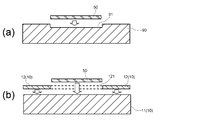
- FIG. 2 shows an assembly drawing in a cross section along the thickness direction (vertical direction) of the substrate when the conventional susceptor 90 is used (a) and when the above susceptor 10 is used (b).
- the susceptor 90 is integrated, but in order to fix the substrate 50 thereon, a recess 91 corresponding to the shape of the substrate 50 is formed on the surface thereof.
- the bottom surface of the recess 91 is flat.
- the thickness of the substrate 50 is, for example, about 430 ⁇ m, and the depth of the concave portion 91 is about 0.5 mm.
- the shape of the substrate 50 can hold the substrate 50 therein, for example, the substrate 50 having a diameter of 2 inches.
- the circular shape is slightly larger than 2 inches in diameter.
- the cross-sectional shape of the recess 91 may be a shape that smoothly supplies and exhausts the source gas to the surface of the substrate 50.
- the surface of the substrate 50 placed and the surface of the surrounding susceptor 90 have almost the same height, which is preferable in this respect.
- the substrate 50 is fixed by being held in the opening 121 (substrate mounting portion) of the upper plate 12. That is, in the susceptor 10, the lower plate 11 corresponds to the conventional susceptor 90 without the recess 91, and the opening 121 of the upper plate 12 corresponds to the recess 91.
- the thickness of the substrate 50 is about 430 ⁇ m, for example, the thickness of the upper plate 12 is about 0.5 mm, which is the same as the depth of the recess 91, and the opening 121 is a circle slightly larger than 2 inches in diameter. It can be a shape.
- the inventor uses a conventional susceptor 90 shown in FIG. 2A to grow a semiconductor layer on a substrate (wafer) 50 having two types of sizes (2 inch diameter and 4 inch diameter), thereby forming a semiconductor.
- the electrical properties and crystallinity of the layer were examined. As a result, in either case, the characteristics (crystallinity and film thickness) were different between the central portion and the peripheral portion of the semiconductor layer.
- the characteristics of the semiconductor layer obtained in the case of the 4-inch diameter in detail, the characteristics of the region corresponding to the 2-inch diameter at the center of the 4-inch diameter wafer are different from the results of the 2-inch diameter wafer. It was very different and almost uniform and showed the same characteristics as the central part.
- the temperature of the surface of the substrate 50 placed on the susceptor 90 varies strictly depending on conditions such as the growth temperature and pressure, but the surroundings It was confirmed that the temperature was about 50 to 100 ° C. lower than the surface temperature of the susceptor.
- this in-plane non-uniformity does not occur on the entire surface of the substrate, but occurs only at the end portion regardless of the size of the substrate. This is considered to be because a region where the temperature increases around the substrate is generated from the result of the temperature measurement. Accordingly, it is considered that in-plane non-uniformity is reduced by using a susceptor having a structure in which a region where the temperature of the substrate is non-uniform is hardly generated.
- FIG. 3 schematically shows the state of heat conduction from the susceptor 90 to the substrate 50 in the conventional configuration of FIG.
- substrate 50 was mounted is expanded and shown, and the arrow in a figure is a direction of heat conduction.
- heat conduction in the vertical direction is heat conduction toward the substrate 50 from the inner surface of the recess 91 that faces the end surface of the substrate 50.
- the substrate 50 is heated not only by heat conduction but also by radiation from the susceptor 90, but this effect is also the same.
- the substrate 50 and the susceptor 90 are in surface contact with each other on the susceptor 90, the placed substrate 50 is fixed only by gravity. For this reason, even if the back surface of the substrate 50 and the surface of the susceptor 90 are both flat, the degree of adhesion between them is low, and the thermal resistance between the substrate 50 and the susceptor 90 is not small. For this reason, although it is preferable that the heat conduction in the vertical direction is dominant as described above, even when the thermal conductivity in the thickness direction of the susceptor 90 and the substrate 50 is both high, the vertical direction is actually The efficiency of heat conduction should not be high.
- the influence of heating by radiation from the susceptor 90 is stronger between the substrate 50 and the susceptor 90 than heat conduction by contact.
- the growth temperature is set to 1000 ° C. or higher as in the case of growing a group III nitride semiconductor, radiation is dominant. This is because heat conduction is determined almost in proportion to the temperature difference between the two objects (the substrate 50 and the susceptor 90), whereas the energy release by radiation is proportional to the fourth power of the temperature of the heat source (susceptor 90). It is. Therefore, in FIG. 3, the influence of heat conduction and radiation from the lateral direction at the end of the substrate 50 cannot be ignored.
- the temperature of the susceptor directly under the substrate when the temperature of the susceptor directly under the substrate is set to a certain temperature, the temperature of the susceptor surface around the substrate (the region where the substrate is not placed) may be equal to or lower than the substrate surface temperature. If possible, it is considered that the temperature non-uniformity at the edge of the substrate is reduced. Since it is the temperature of the substrate surface that directly affects crystal growth, the temperature of the susceptor may be set higher than the desired temperature so that the surface temperature of the substrate becomes the desired temperature. .
- the lower plate 11 is used as a portion corresponding to the conventional susceptor 90.
- the lower plate 11 and the upper plate 12 are used separately.
- a concave portion is provided so that a part of the lower plate 11 having a high temperature does not face the inner surface of the substrate 50 in a state where the substrate 50 is placed on the lower plate 11. Absent. That is, unlike the susceptor 90, the surface of the lower plate 11 is flat. Instead, the inner surface of the opening 121 of the upper plate 12 faces the side surface of the substrate 50.
- the upper plate 12 As with the substrate 50, the upper plate 12 is placed on the lower plate 11 by gravity. For this reason, the thermal resistance between the upper plate 12 and the lower plate 11 is similarly high as between the substrate 50 and the lower plate 11. Furthermore, since the heat conductivity of the upper plate 12 is set lower than that of the lower plate 11 and the substrate 50, the heat conduction efficiency to the upper plate 12 is further lower than the heat conduction efficiency to the substrate 50, The temperature of the surface of the plate 12 can be lowered. Further, the temperature of the inner surface of the opening 121 facing the side surface of the substrate 50 is lower than the temperature of the inner surface of the recess 91 in the conventional susceptor 90. Therefore, the influence of the lateral heat conduction and radiation from the upper plate 12 on the substrate 50 in the configuration of FIG.
- the susceptor 10 is installed in a chamber, and a semiconductor layer is formed on the substrate 50 in the chamber.
- the reaction product adheres to the inner wall of the chamber.
- it is generally necessary to perform maintenance such as replacement and cleaning of the chamber to which the reaction product adheres at an appropriate frequency.
- the susceptor 10 when used, the surface temperature of the upper plate 12 is lowered, so that the temperature of the inner wall of the chamber facing it is also lowered. For this reason, the amount of reaction products adhering to the inner wall of the chamber is also reduced.
- the amount of the reaction product adhering to the susceptor 10 and the chamber can be reduced, so that the frequency of maintenance can be reduced, and the upper plate to which the reaction product adheres. 12 can be easily replaced and cleaned.
- the upper plate 12 it is also possible to configure the upper plate 12 with a material that makes this cleaning particularly easy.
- the reaction product is, for example, AlInGaN having a thermal expansion coefficient of about 4 to 6 ppm / K
- the thermal expansion coefficient Due to the difference, it is particularly easy to peel and clean the reaction product.
- the thermal conductivity of the material of the substrate 50 is generally lower than this.
- a material having a lower thermal conductivity can be appropriately used depending on the material of the substrate 50.
- SiC thermal conductivity in a temperature range of 1000 ° C. or higher to about 70 W / m / K
- TaC standard as about 9 to 22 W / K
- the upper plate 12 needs to be made of a material that does not react with the gas used (such as ammonia or hydrogen) or has low reactivity. In this respect, any of the above materials can be used without any problem. The same applies to the lower plate 11.
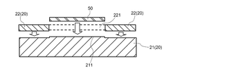
- FIG. 4 shows an assembly drawing in a cross section of a susceptor 20 which is a modification of the susceptor 10 as a reference example.
- a lower plate 21 and an upper plate 22 are used, and heat conduction to the upper plate 22 is further suppressed.
- the material which comprises the lower plate 21 and the upper plate 22 is the same as the said lower plate 11 and the upper plate 12, respectively, and only the shapes differ.
- the substrate mounting portion 211 which is a region on which the substrate 50 is mounted, is made higher than its surroundings.
- the surface of the lower plate 21 other than the substrate platform 211 is configured to be deeper than the substrate platform 211.
- the surface of the substrate platform 211 is flat like the surface of the lower plate 11.
- an opening 221 corresponding to the substrate 50 is formed in the same manner as the upper plate 12.
- the opening 221 is set so as to correspond to the substrate mounting portion 211. That is, when the susceptor 20 is used, the substrate 50 is mounted on the substrate platform 211 in the opening 221.
- the area other than the substrate platform 211 in the lower plate 21 has a shape dug down from the substrate platform 211. Therefore, when the height relationship between the upper surface of the upper plate 22 and the upper surface of the substrate 50 in the state where the upper plate 22 and the lower plate 21 are combined is made the same as that of the susceptor 10, the upper plate 22 is The thickness of the lower plate 21 can be increased by the amount dug. That is, the upper plate 22 can be made thicker than the susceptor 10 described above. Since the upper plate 22 having a low thermal conductivity becomes thick, the temperature of the surface of the upper plate 22 can be further reduced. For this reason, the nonuniformity of the temperature in the edge part of the board
- the upper plate 22 is installed on the lower plate 21. Fixing is performed more reliably.
- the thickness of the substrate 50 is reduced.
- the thermal conductivity is ⁇ S
- the thickness of the upper plate 22 (12) is T TP
- the thermal conductivity is ⁇ TP
- the upper limit of the thickness T TP of the upper plate 22 (12) is, for example, about 2000 ⁇ m.
- the lower limit of the thickness of the upper plates 12 and 22 is set to a thickness that can be manufactured as a thin plate that is portable depending on the material, for example, PG Then, it is about 200 ⁇ m.
- the value of TTP is set in consideration of the equation (1), the total thickness of the susceptors 10 and 20 (total thickness when the upper plates 12 and 22 are placed on the lower plates 11 and 21) Is set depending on the thicknesses of the lower plates 11 and 21 as well. However, the warpage is suppressed as the upper plates 12 and 22 are thicker.
- the height of the upper surface of the substrate and the height of the upper surface of the upper plate are not necessary to make the height of the upper surface of the substrate and the height of the upper surface of the upper plate exactly match.
- the temperature of the upper surface of the upper plate can be further lowered.
- the temperature of the upper surface of the upper plate can be made lower than that of the conventional susceptor.
- the temperature distribution on the upper surface of the susceptor including the wafer is adjusted, and in particular, the temperature of the upper surface of the upper plate is lowered, so that the growth layer on the substrate is uniform in the plane. Had improved.
- the susceptor having this configuration is used, there are some cases where cracks are formed at the outermost end (outer peripheral portion) of the growth layer.
- the temperature distribution in the most region of the growth layer can be made uniform by the above configuration, while the temperature gradient in the outer peripheral portion (endmost portion) of the growth layer is conversely increased. Conceivable.
- the susceptor according to the embodiment of the present invention is configured so that a uniform growth layer is obtained and the temperature gradient in the outer peripheral portion of the substrate is reduced in order to solve this problem.
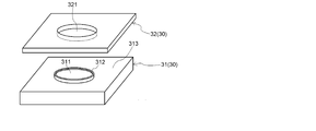
- FIG. 5 is a perspective view of the susceptor 30 according to the embodiment of the present invention before the assembly of the lower plate 31, the upper plate 32, and the substrate 50
- FIG. 6 is the state before assembly (a) and after assembly (b). It is sectional drawing along the thickness direction of the board
- FIG. Here, like the upper plate 22 in FIG. 4, a circular opening 321 is formed in the upper plate 32, and the substrate placing portion 311 in the lower plate 31 is also a surface on which the upper plate 32 is placed. Is set higher than.
- the heat conductivity of the lower plate 31 and the upper plate 32 it sets similarly to the said reference example. For this reason, the temperature uniformity over most of the substrate 50 can be improved, and the uniformity of the growth layer can be improved as in the above-described reference example.
- an outer peripheral projection 312 is formed on the outer periphery of the substrate platform 311 so as to surround the substrate platform 311.
- the substrate platform 311 is a bottom surface of a recess formed in the lower plate 31, and the substrate 50 is placed in this recess. That is, the lower plate 31 is shaped such that the substrate 50 is fitted inside the outer periphery protruding portion 312.
- the opening 321 in the upper plate 32 corresponds to the outer diameter of the outer peripheral projection 312, not the substrate 50, and has a shape that fits thereto.
- the top of the outer peripheral projection 312 is a plane parallel to the substrate platform 311 and the like.
- the lower plate upper surface (the upper surface of the lower plate 31) 313 of the lower plate 31 outside the outer peripheral projection 312 can be formed in a planar shape, for example. Further, when the substrate 50 and the upper plate 32 are installed on the lower plate 31, they contact the lower surface of the upper plate (the lower surface of the upper plate 32) 322 in the upper plate 32.
- the lower plate upper surface 313 and the upper plate lower surface 322 that are in contact with each other can have a planar shape, for example. However, if the source gas does not easily enter the interface when they are in contact with each other, the upper surface is not necessary. At this time, as viewed from above, the upper surface of the substrate 50 and the top of the outer peripheral projection 312 are exposed from the upper plate 32.
- the inner periphery of the upper plate 12 constituting the opening 121 and the outer periphery of the substrate 50 face each other directly, whereas the opening 321 is configured.
- an outer peripheral projection 312 integrated with the lower plate 31 is provided between the inner periphery of the upper plate 32 and the outer periphery of the substrate 50.
- the depth T (the height of the outer peripheral projection 312 from the substrate mounting portion 311) in FIG. 6 is equal to the thickness of the substrate 50 (for example, about 0.43 mm).
- the thickness D of the upper plate 32 is the same as the height of the outer peripheral protrusion 312 from the outer side of the outer peripheral protrusion 312 (the surface on which the upper plate 32 is placed) in the lower plate 31.
- the thickness D is eventually thicker than the substrate 50 and can be about 2 mm.
- the upper surface of the upper plate 32 and the substrate 50 constitute the same surface on the lower plate 31 in the assembled state. Further, the substrate 50 is supported only by the lower plate 31, not the upper plate 32.
- the materials constituting the lower plate 31 and the upper plate 32 and their thermal conductivity are the same as those in the reference example. That is, for example, the lower plate 31 can be made of graphite coated with thin PG, and the upper plate can be made of PG.
- the outer peripheral projection 312 is a part of the lower plate 31, the outer peripheral projection 312 is locally protruded upward, so the temperature of the outer peripheral projection 312 is Is not equal to the main body of the lower lower plate 31 and is lower than this.
- the temperature of the outer peripheral projection 312 is determined by the lower plate 31 main body, the upper plate 32, and the substrate 50 which are lower than this. Therefore, a region having a large temperature gradient in the outer peripheral portion of the growth layer when the susceptor according to the first embodiment is used is formed in the outer peripheral protrusion 312. Since a region having a large temperature gradient is not formed in the substrate 50, generation of cracks in the outer peripheral portion of the growth layer is suppressed.
- the width W in the left-right direction in FIG. 6 of the outer peripheral projection 312 is preferably 1 to 5 mm, and more preferably 1 to 3 mm.
- the width W is less than 1.0 mm, the effect of reducing the temperature gradient in the outermost region of the substrate 50 is reduced. If the width W exceeds 5 mm, the uniformity of the growth layer decreases because the width W substantially approaches the conventional susceptor 90 (FIG. 2A).
- the upper surface of the substrate 50 and the upper surface of the upper plate 32 have the same height.
- the height is preferably the same as these.
- the upper plate 32 can be made thicker than in the first embodiment.
- the upper plate 32 since the upper surface side of the upper plate 32 is exposed to the source gas during growth, a reaction product layer is formed on the upper surface of the upper plate 32. Due to the difference in thermal expansion coefficient between the reaction product layer and the upper plate 32, the upper plate 32 may be warped during heating (during growth). Problems such as poor reproducibility occur. In order to suppress this, it is effective to make the upper plate 32 sufficiently thick. In the above configuration, such a thick upper plate 32 can be used even when the substrate 50 is thin. That is, in this susceptor 30, the upper plate 32 in which warpage is suppressed due to its thickness can be used. Thereby, reproducibility of crystal growth can be improved.
- the case where one substrate is placed on one set of susceptors has been described.
- a plurality of substrates can be appropriately disposed.
- an opening in the upper plate, a substrate mounting portion in the lower plate, and the like may be formed according to the configuration in which the substrate is arranged.
- the above structure can provide higher temperature uniformity in each substrate, and thereby a semiconductor layer having high in-plane uniformity can be obtained.
- the susceptor and individual substrates may be rotated in order to improve the uniformity between the substrates. In this case, the same effect can be obtained. it is obvious.
- the configuration of the susceptor in the region between the substrates can be set as appropriate.
- the distance between the substrates is narrow (when the closest distance between the substrates is 0 to 5 mm)
- the above-described substrate placement is obtained by integrating the substrate placement portions corresponding to two adjacent substrates. It can also be considered a department.
- the openings 321 corresponding to the two adjacent substrates can be continuously formed so that the upper plate does not exist between the two substrates.
- the closest distance is particularly narrow, such as less than 1 mm
- the outer peripheral projection is not provided between the substrates, and the outer peripheral projection is provided only around the integrated substrate mounting portion. Can do. The same applies when three or more substrates are used.
- the upper plate is shaped so that the upper surface of the placed substrate and the top of the outer peripheral projection are exposed on the upper surface side of the upper plate.
- Such a configuration is effective when, for example, a large number of substrates (wafers) having a relatively small diameter of 2 to 3 inches are arranged.
- the effects of the configuration around the substrate in the reference example and the susceptor according to the above embodiment are not Relatively small.
- the area where the lower plate is exposed increases when a plurality of substrates are arranged close to each other. For this reason, the effect of the configuration around the substrate in the reference example and the susceptor according to the above-described embodiment is increased. That is, the susceptor of the present invention is particularly effective when a plurality of substrates are arranged and a large-diameter substrate is used.
- the upper plate is preferably made of a single material such as PG, but it is not always necessary.
- a thick surface protective layer may be formed on the composite material, for example, the base material.
- graphite can be used as a base material and PG having a low thermal conductivity can be thickly coated (thick enough to become a main material) to form the upper plate.
- PG is used as a base material, and pBN (thermal conductivity: about 2.7 W / m / K), which is difficult to form an upper plate because it is soft as a single body, can be coated thereon.
- the surface temperature of the upper plate can be made lower than the surface temperature of the substrate, and the same effect can be obtained.
- the upper plate is generally composed of a single material because peeling, cracking, and deterioration of durability due to the difference in thermal expansion coefficient between the base material and the coating layer occur.
- PG is particularly preferable as the material.
- a sapphire substrate is placed on a susceptor of two types shown in FIG. 2 (a: comparative example) (b: reference example) and placed in a chamber.
- Carrier gas N 2 and H 2
- the susceptor was heated using a heater below the susceptor, and AlN crystals were grown on the sapphire substrate under the same conditions except for the susceptor.
- a sapphire substrate having a diameter of 2 inches and a thickness of 430 ⁇ m (vertical thermal conductivity in a temperature range of 1000 ° C. or higher: about 8 W / m / K) was used, and TMA and NH 3 were used as source gases.
- the material of the comparative susceptor is 6.5 mm thick graphite (thermal conductivity in the vertical direction in the temperature range of 1000 ° C. or higher: 40 to 100 W / m / K), and the surface is coated with 150 ⁇ m of pBN. .
- the depth of the recess is 0.5 mm.
- the lower plate of the reference example has a flat plate structure with a thickness of 6 mm, and the material is the same as the susceptor of the comparative example.
- the material of the upper plate of the reference example is PG (thermal conductivity in the vertical direction in a temperature range of 1000 ° C. or higher: about 1.5 W / m / K), and the thickness is 0.5 mm.
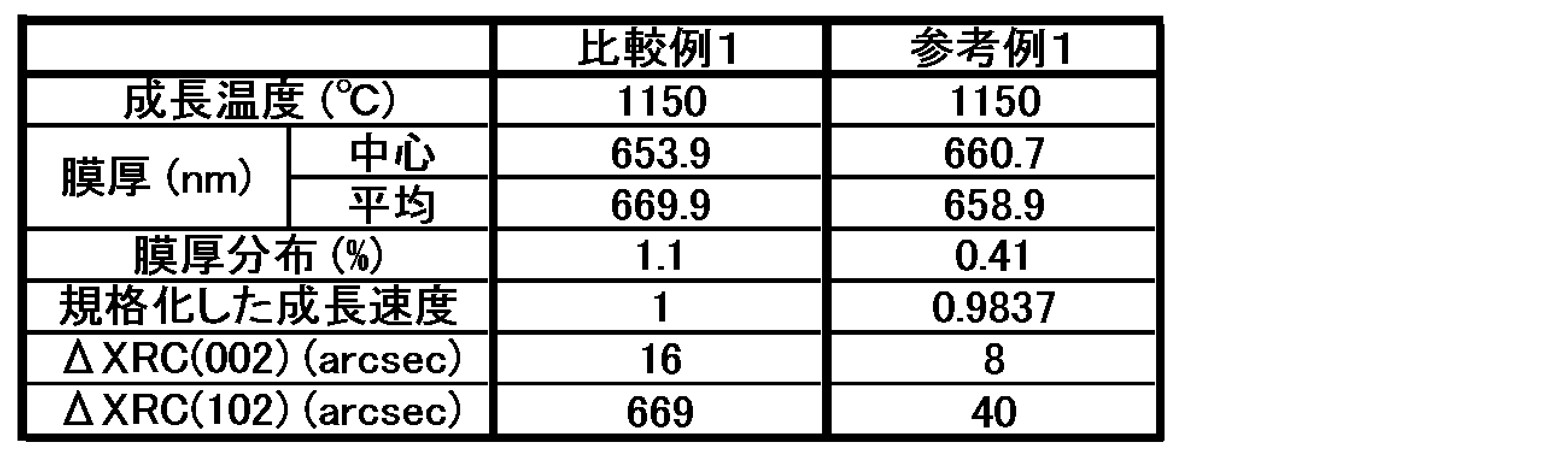
- the measurement results for the semiconductor layers obtained using the susceptors of the comparative example and the reference example are shown in comparative example 1 and reference example 1 of Table 1.
- the growth temperature (actual substrate surface temperature measured without contact) was 1150 ° C.
- the film thickness distribution of the semiconductor layer was measured at a total of 25 locations including the central one point in the 2-inch diameter plane, and the film thickness distribution according to the following equation was calculated as uniformity.
- the center of the full width at half maximum (FWHM) (arcsec) of the X-ray diffraction rocking curve (XRC) of the (002) plane of the semiconductor layer (AlN) and four points 20 mm away from the center The difference between the maximum value and the minimum value ( ⁇ XRC (002)) of the measured values at a total of five points, and the difference between the maximum value and the minimum value ( ⁇ XRC (102)) obtained in the same manner for the (102) plane were measured.
- the susceptor of the comparative example in order to remove AlN adhering to the susceptor, it was necessary to immerse in an alkaline solution, and cleaning for reuse was not easy.
- the AlN adhering to the upper plate can be removed only by stroking with a light force using a wiper or the like, and cleaning was easy.
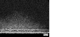
- AlN layer having a thickness of 1.0 ⁇ m was formed on the sapphire substrate in the same manner as in Reference Example 1 except that the growth temperature was set to 1300 ° C. and the pressure was set to 10 Torr using the susceptor of Reference Example. To grow. As a result, although a highly uniform growth layer (AlN layer) was obtained in the same manner as in Reference Example 1, cracks occurred at the outer peripheral edge. An optical micrograph of the surface is shown in FIG. In FIG. 7, the gray region is the growth layer, and the boundary line between this region and the black region is the end of the growth layer. There are some cracks from the lower left to the upper right.
- this crack is formed only in a very narrow area at the end, and the device is formed at a position away from the center toward the center of the wafer. It is more preferable that the cracks are suppressed because the cracks may propagate and cause a substrate crack.
- Example 1 crystal growth was performed under the same growth conditions as in Reference Example 2 using the susceptor.
- the thickness as a whole susceptor of an Example is 6.5 mm same as the susceptor of a comparative example and a reference example.
- the warpage of the upper plate after the crystal growth of the upper plate or during the crystal growth was also reduced.
- the upper plate thickness is 0.5 mm
- the susceptor of the example In Example 1 using (upper plate thickness 2 mm) no wafer movement occurred. That is, also from the viewpoint of warping of the upper plate, good results were obtained when the susceptor of the example was used.
- Example 2 Comparative Example 2, and Reference Example 3
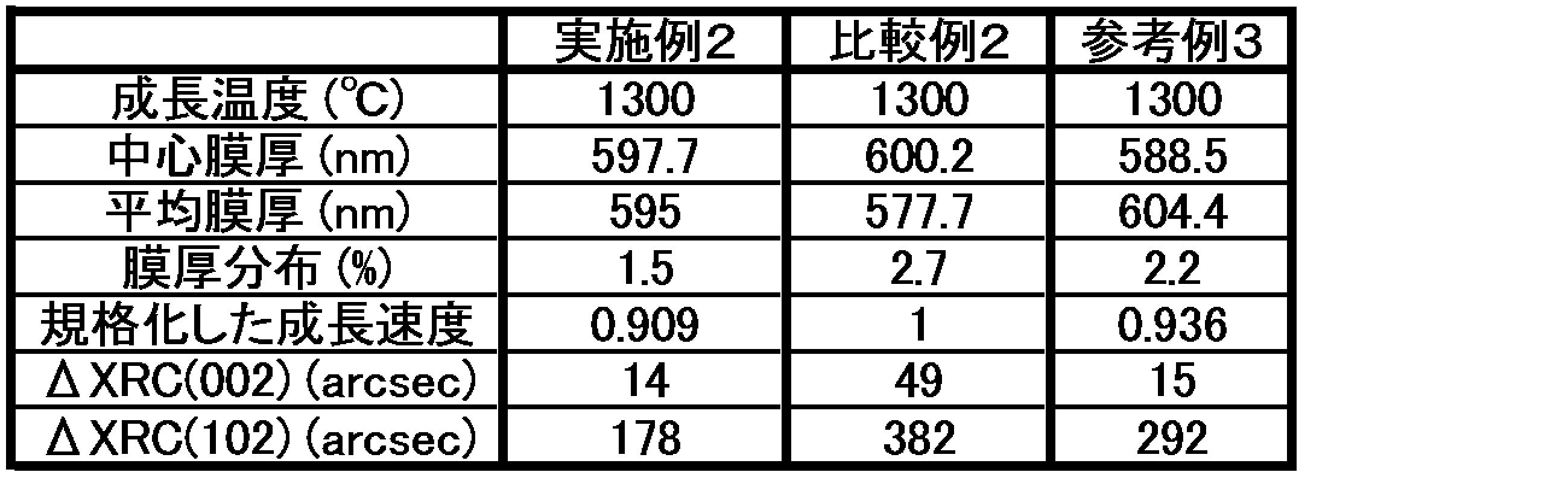
- crystal growth was performed using the susceptors of Examples, Comparative Examples, and Reference Examples at a growth temperature of 1300 ° C. and a pressure of 10 Torr.
- the evaluation results of evaluating the film thickness distribution and crystallinity in the same manner as in Reference Example 1 are shown in Table 2. From this result, although the average growth rate is lowered in Example 2 and Reference Example 3, the values of the film thickness distribution and crystallinity are smaller than those in Comparative Example 2, and the film thickness distribution and crystallinity. It can be seen that is improved. Further, comparing Example 2 with Reference Example 3, it can be seen that Example 2 has a greater improvement effect.
- the growth layer is not limited to a semiconductor layer and can be made of any material.
- the growth layer has a laminated structure of a plurality of layers, and the growth temperature of each layer is the same or different, it is clear that the above effect can be obtained by the above configuration in at least one layer. It is. In the above example, the case where the MOCVD method is used is described. However, it is obvious that the same effect can be obtained regardless of the type of gas if the CVD method is a method in which a source gas is reacted on a high-temperature substrate.
Landscapes
- Chemical & Material Sciences (AREA)
- Engineering & Computer Science (AREA)
- Materials Engineering (AREA)
- Metallurgy (AREA)
- Organic Chemistry (AREA)
- General Chemical & Material Sciences (AREA)
- Chemical Kinetics & Catalysis (AREA)
- Mechanical Engineering (AREA)
- Crystallography & Structural Chemistry (AREA)
- Inorganic Chemistry (AREA)
- Container, Conveyance, Adherence, Positioning, Of Wafer (AREA)
- Chemical Vapour Deposition (AREA)
Abstract
Description
本発明のサセプタは、基板を保持し、当該基板上に化学気相成長(CVD)法によって成長層を形成するためのサセプタであって、前記サセプタは、下部プレートと当該下部プレートの上面に設置される上部プレートとを有し、前記下部プレートは、前記下部プレートの上面に前記基板が載置される領域である基板載置部を具備し、さらに、前記基板載置部の周囲に、前記基板が前記基板載置部上において囲まれる形状となるように形成された外周突起部を具備し、前記上部プレートは、前記下部プレートの上面の前記基板載置部及び前記外周突起部を除く領域に載置され、前記基板載置部と前記外周突起部の頂部とを前記上部プレートの上面側に露出させる形状を具備し、前記上部プレートの上下方向における熱伝導率は、前記下部プレートの上下方向における熱伝導率よりも低いことを特徴とする。
本発明のサセプタにおいて、前記基板載置部において前記基板が載置される面は、前記上部プレートが載置される前記下部プレートの上面よりも高く設定され、前記下部プレートと前記上部プレートとを組み合わせた際に、前記上部プレートの上面と前記外周突起部の頂部とが同一の高さとなるように設定されたことを特徴とする。
本発明のサセプタにおいて、前記外周突起部の幅は1.0mm~5.0mmの範囲であることを特徴とする。
本発明のサセプタにおいて、前記上部プレートを構成する主な材料はパイロリテックグラファイト(熱分解炭素)であることを特徴とする。
本発明のサセプタは、前記下部プレートの表面に、表面保護層を具備することを特徴とする。
本発明のサセプタにおいて、前記表面保護層はパイロリティックボロンナイトライド(pBN)またはシリコンカーバイド(SiC)で構成されたことを特徴とする。
本発明の結晶成長装置は、サセプタの上に基板が載置され、当該基板上に化学気相成長法によって成長層を形成する結晶成長装置であって、前記サセプタは、下部プレートと当該下部プレートの上面に設置される上部プレートとを有し、前記下部プレートは、前記下部プレートの上面に前記基板が載置される領域である基板載置部を具備し、さらに、前記基板載置部の周囲に、前記基板が前記基板載置部上において囲まれる形状となるように形成された外周突起部を具備し、前記上部プレートは、前記下部プレートの上面の前記基板載置部及び前記外周突起部を除く領域に載置され、前記基板の上面と前記外周突起部の頂部とを前記上部プレートの上面側に露出させる形状を具備し、前記上部プレートの上下方向における熱伝導率は、前記下部プレート及び前記基板の上下方向における熱伝導率よりも低いことを特徴とする。
本発明の結晶成長装置において、前記基板載置部において前記基板が載置される面は、前記上部プレートが載置される前記下部プレートの上面よりも高く設定され、前記下部プレート、前記基板、及び前記上部プレートを組み合わせた際に、前記上部プレートの上面、前記基板の上面、及び前記外周突起部の頂部が同一の高さとなるように設定されたことを特徴とする。
本発明の結晶成長装置において、前記外周突起部の幅は1.0mm~5.0mmの範囲であることを特徴とする。
本発明の結晶成長装置において、前記下部プレートを構成する主な材料は黒鉛、前記上部プレートを構成する主な材料はパイロリテックグラファイト(熱分解炭素)であることを特徴とする。
本発明の結晶成長装置は、前記下部プレートの表面に、表面保護層を具備することを特徴とする。
本発明の結晶成長装置において、前記表面保護層はパイロリティックボロンナイトライド(pBN)またはシリコンカーバイド(SiC)で構成されたことを特徴とする。
本発明の結晶成長方法は、前記結晶成長装置を用い、チャンバ内において、前記下部プレートを加熱して、前記基板が前記サセプタの上に載置され加熱された状態で前記成長層の原料が含まれる原料ガスを流すことを特徴とする。
本発明の結晶成長方法において、前記基板はサファイアであり、前記成長層の成長時の前記基板の温度を1000℃以上とすることを特徴とする。
本発明の結晶成長方法において、前記成長層は窒化物半導体であることを特徴とする。

上記の参考例となるサセプタにおいては、上記の通り、ウェハを含めたサセプタの上面の温度分布を調整し、特に上部プレートの上面の温度を低下させることによって、基板上の成長層の面内均一性を向上させていた。ただし、この構成のサセプタを用いた場合には、成長層の最端部(外周部)にクラックが形成される場合が散見された。これは、上記の構成によって成長層の大部分の領域における温度分布を均一にすることができる一方で、成長層の外周部(最端部)における温度勾配は逆に大きくなっていることによると考えられる。すなわち、上記の構成によって、温度勾配の大きな領域は基板上の広い範囲においては除去されているものの、基板上における最端部に近い狭い領域には温度勾配の大きな領域が形成されていると考えられる。そこで、本発明の実施の形態となるサセプタにおいては、これを解消するために、均一な成長層が得られると共に、基板の外周部における温度勾配が小さくなるような構成とされる。

11、21、31 下部プレート
12、22、32 上部プレート
50 基板
91 凹部
121、221、321 開口部
211、311 基板載置部
312 外周突起部
313 下部プレート上面(下部プレートの上面)
322 上部プレート下面(上部プレートの下面)
Claims (15)
- 基板を保持し、当該基板上に化学気相成長(CVD)法によって成長層を形成するためのサセプタであって、
前記サセプタは、下部プレートと当該下部プレートの上面に設置される上部プレートとを有し、
前記下部プレートは、前記下部プレートの上面に前記基板が載置される領域である基板載置部を具備し、さらに、前記基板載置部の周囲に、前記基板が前記基板載置部上において囲まれる形状となるように形成された外周突起部を具備し、
前記上部プレートは、前記下部プレートの上面の前記基板載置部及び前記外周突起部を除く領域に載置され、前記基板載置部と前記外周突起部の頂部とを前記上部プレートの上面側に露出させる形状を具備し、
前記上部プレートの上下方向における熱伝導率は、前記下部プレートの上下方向における熱伝導率よりも低いことを特徴とするサセプタ。 - 前記基板載置部において前記基板が載置される面は、前記上部プレートが載置される前記下部プレートの上面よりも高く設定され、前記下部プレートと前記上部プレートとを組み合わせた際に、前記上部プレートの上面と前記外周突起部の頂部とが同一の高さとなるように設定されたことを特徴とする請求項1に記載のサセプタ。
- 前記外周突起部の幅は1.0mm~5.0mmの範囲であることを特徴とする請求項1又は2に記載のサセプタ。
- 前記上部プレートを構成する主な材料はパイロリテックグラファイト(熱分解炭素)であることを特徴とする請求項1から請求項3までのいずれか1項に記載のサセプタ。
- 前記下部プレートの表面に、表面保護層を具備することを特徴とする請求項1から請求項4までのいずれか1項に記載のサセプタ。
- 前記表面保護層はパイロリティックボロンナイトライド(pBN)またはシリコンカーバイド(SiC)で構成されたことを特徴とする請求項5に記載のサセプタ。
- サセプタの上に基板が載置され、当該基板上に化学気相成長法によって成長層を形成する結晶成長装置であって、
前記サセプタは、下部プレートと当該下部プレートの上面に設置される上部プレートとを有し、
前記下部プレートは、前記下部プレートの上面に前記基板が載置される領域である基板載置部を具備し、さらに、前記基板載置部の周囲に、前記基板が前記基板載置部上において囲まれる形状となるように形成された外周突起部を具備し、
前記上部プレートは、前記下部プレートの上面の前記基板載置部及び前記外周突起部を除く領域に載置され、前記基板の上面と前記外周突起部の頂部とを前記上部プレートの上面側に露出させる形状を具備し、
前記上部プレートの上下方向における熱伝導率は、前記下部プレート及び前記基板の上下方向における熱伝導率よりも低いことを特徴とする結晶成長装置。 - 前記基板載置部において前記基板が載置される面は、前記上部プレートが載置される前記下部プレートの上面よりも高く設定され、前記下部プレート、前記基板、及び前記上部プレートを組み合わせた際に、前記上部プレートの上面、前記基板の上面、及び前記外周突起部の頂部が同一の高さとなるように設定されたことを特徴とする請求項7に記載の結晶成長装置。
- 前記外周突起部の幅は1.0mm~5.0mmの範囲であることを特徴とする請求項7又は8に記載の結晶成長装置。
- 前記下部プレートを構成する主な材料は黒鉛、前記上部プレートを構成する主な材料はパイロリテックグラファイト(熱分解炭素)であることを特徴とする請求項7から請求項9までのいずれか1項に記載の結晶成長装置。
- 前記下部プレートの表面に、表面保護層を具備することを特徴とする請求項7から請求項10までのいずれか1項に記載の結晶成長装置。
- 前記表面保護層はパイロリティックボロンナイトライド(pBN)またはシリコンカーバイド(SiC)で構成されたことを特徴とする請求項11に記載の結晶成長装置。
- 請求項7から請求項12までのいずれか1項に記載の結晶成長装置を用い、
チャンバ内において、前記下部プレートを加熱して、前記基板が前記サセプタの上に載置され加熱された状態で前記成長層の原料が含まれる原料ガスを流すことを特徴とする結晶成長方法。 - 前記基板はサファイアであり、前記成長層の成長時の前記基板の温度を1000℃以上とすることを特徴とする請求項13に記載の結晶成長方法。
- 前記成長層は窒化物半導体であることを特徴とする請求項13又は14に記載の結晶成長方法。
Priority Applications (3)
| Application Number | Priority Date | Filing Date | Title |
|---|---|---|---|
| CN201380039771.5A CN104641454A (zh) | 2012-07-26 | 2013-07-26 | 基座、结晶生长装置以及结晶生长方法 |
| JP2014527036A JP6062436B2 (ja) | 2012-07-26 | 2013-07-26 | サセプタ、結晶成長装置および結晶成長方法 |
| US14/417,329 US20150206785A1 (en) | 2012-07-26 | 2013-07-26 | Susceptor, crystal growth apparatus, and crystal growth method |
Applications Claiming Priority (2)
| Application Number | Priority Date | Filing Date | Title |
|---|---|---|---|
| JP2012-165692 | 2012-07-26 | ||
| JP2012165692 | 2012-07-26 |
Publications (1)
| Publication Number | Publication Date |
|---|---|
| WO2014017650A1 true WO2014017650A1 (ja) | 2014-01-30 |
Family
ID=49997454
Family Applications (1)
| Application Number | Title | Priority Date | Filing Date |
|---|---|---|---|
| PCT/JP2013/070373 Ceased WO2014017650A1 (ja) | 2012-07-26 | 2013-07-26 | サセプタ、結晶成長装置および結晶成長方法 |
Country Status (4)
| Country | Link |
|---|---|
| US (1) | US20150206785A1 (ja) |
| JP (1) | JP6062436B2 (ja) |
| CN (1) | CN104641454A (ja) |
| WO (1) | WO2014017650A1 (ja) |
Cited By (5)
| Publication number | Priority date | Publication date | Assignee | Title |
|---|---|---|---|---|
| JP2016204201A (ja) * | 2015-04-22 | 2016-12-08 | シャープ株式会社 | 窒化物半導体エピタキシャルウェハおよびその製造方法 |
| JPWO2017043165A1 (ja) * | 2015-09-11 | 2017-09-07 | 住友電気工業株式会社 | 炭化珪素エピタキシャル基板および炭化珪素半導体装置の製造方法 |
| KR20180031796A (ko) * | 2015-08-17 | 2018-03-28 | 어플라이드 머티어리얼스, 인코포레이티드 | 공간적 원자층 증착을 위한 가열원 |
| JP2018082100A (ja) * | 2016-11-17 | 2018-05-24 | 昭和電工株式会社 | 搭載プレート、ウェハ支持台、及び化学気相成長装置 |
| JP2021190688A (ja) * | 2020-05-28 | 2021-12-13 | 環球晶圓股▲ふん▼有限公司Global Wafers Co., Ltd. | ウェハマウントステーションおよびウェハ埋め込み構造の形成方法 |
Families Citing this family (6)
| Publication number | Priority date | Publication date | Assignee | Title |
|---|---|---|---|---|
| KR102417181B1 (ko) * | 2015-11-09 | 2022-07-05 | 삼성전자주식회사 | 발광 패키지, 반도체 발광 소자, 발광 모듈 및 발광 패키지의 제조 방법 |
| DE102016115614A1 (de) * | 2016-08-23 | 2018-03-01 | Aixtron Se | Suszeptor für einen CVD-Reaktor |
| CN107785243B (zh) * | 2016-08-26 | 2023-06-20 | 住友电工光电子器件创新株式会社 | 形成氮化物半导体层的工艺 |
| US10947640B1 (en) * | 2016-12-02 | 2021-03-16 | Svagos Technik, Inc. | CVD reactor chamber with resistive heating for silicon carbide deposition |
| US20200385864A1 (en) * | 2017-10-18 | 2020-12-10 | Nippon Techno-Carbon Co., Ltd. | Susceptor |
| KR102580723B1 (ko) | 2017-12-13 | 2023-09-21 | 에이에스엠엘 네델란즈 비.브이. | 리소그래피 장치에서 사용하기 위한 기판 홀더 |
Citations (7)
| Publication number | Priority date | Publication date | Assignee | Title |
|---|---|---|---|---|
| JPS6318079A (ja) * | 1986-07-10 | 1988-01-25 | Toshiba Corp | 薄膜形成方法及び装置 |
| JPH02186622A (ja) * | 1989-01-13 | 1990-07-20 | Toshiba Ceramics Co Ltd | サセプタ |
| JPH0547670A (ja) * | 1991-06-20 | 1993-02-26 | Ibiden Co Ltd | 常圧cvd装置のための黒鉛製ウエハ保持治具 |
| JP2006173560A (ja) * | 2004-11-16 | 2006-06-29 | Sumitomo Electric Ind Ltd | ウエハガイド、有機金属気相成長装置および窒化物系半導体を堆積する方法 |
| JP2009194045A (ja) * | 2008-02-13 | 2009-08-27 | Taiyo Nippon Sanso Corp | 気相成長装置 |
| JP2009252969A (ja) * | 2008-04-04 | 2009-10-29 | Sumitomo Electric Ind Ltd | サセプタおよび気相成長装置 |
| JP2012044030A (ja) * | 2010-08-20 | 2012-03-01 | Showa Denko Kk | 化合物半導体の製造装置、化合物半導体の製造方法及び化合物半導体 |
Family Cites Families (2)
| Publication number | Priority date | Publication date | Assignee | Title |
|---|---|---|---|---|
| JP4245983B2 (ja) * | 2003-05-28 | 2009-04-02 | 助川電気工業株式会社 | 黒鉛真空容器 |
| JP5787526B2 (ja) * | 2011-01-17 | 2015-09-30 | イビデン株式会社 | 電子部品位置決め用治具 |
-
2013
- 2013-07-26 US US14/417,329 patent/US20150206785A1/en not_active Abandoned
- 2013-07-26 CN CN201380039771.5A patent/CN104641454A/zh active Pending
- 2013-07-26 WO PCT/JP2013/070373 patent/WO2014017650A1/ja not_active Ceased
- 2013-07-26 JP JP2014527036A patent/JP6062436B2/ja active Active
Patent Citations (7)
| Publication number | Priority date | Publication date | Assignee | Title |
|---|---|---|---|---|
| JPS6318079A (ja) * | 1986-07-10 | 1988-01-25 | Toshiba Corp | 薄膜形成方法及び装置 |
| JPH02186622A (ja) * | 1989-01-13 | 1990-07-20 | Toshiba Ceramics Co Ltd | サセプタ |
| JPH0547670A (ja) * | 1991-06-20 | 1993-02-26 | Ibiden Co Ltd | 常圧cvd装置のための黒鉛製ウエハ保持治具 |
| JP2006173560A (ja) * | 2004-11-16 | 2006-06-29 | Sumitomo Electric Ind Ltd | ウエハガイド、有機金属気相成長装置および窒化物系半導体を堆積する方法 |
| JP2009194045A (ja) * | 2008-02-13 | 2009-08-27 | Taiyo Nippon Sanso Corp | 気相成長装置 |
| JP2009252969A (ja) * | 2008-04-04 | 2009-10-29 | Sumitomo Electric Ind Ltd | サセプタおよび気相成長装置 |
| JP2012044030A (ja) * | 2010-08-20 | 2012-03-01 | Showa Denko Kk | 化合物半導体の製造装置、化合物半導体の製造方法及び化合物半導体 |
Cited By (8)
| Publication number | Priority date | Publication date | Assignee | Title |
|---|---|---|---|---|
| JP2016204201A (ja) * | 2015-04-22 | 2016-12-08 | シャープ株式会社 | 窒化物半導体エピタキシャルウェハおよびその製造方法 |
| KR20180031796A (ko) * | 2015-08-17 | 2018-03-28 | 어플라이드 머티어리얼스, 인코포레이티드 | 공간적 원자층 증착을 위한 가열원 |
| JP2018533201A (ja) * | 2015-08-17 | 2018-11-08 | アプライド マテリアルズ インコーポレイテッドApplied Materials,Incorporated | 空間的原子層堆積用の加熱源 |
| KR102796880B1 (ko) * | 2015-08-17 | 2025-04-15 | 어플라이드 머티어리얼스, 인코포레이티드 | 공간적 원자층 증착을 위한 가열원 |
| JPWO2017043165A1 (ja) * | 2015-09-11 | 2017-09-07 | 住友電気工業株式会社 | 炭化珪素エピタキシャル基板および炭化珪素半導体装置の製造方法 |
| JP2018082100A (ja) * | 2016-11-17 | 2018-05-24 | 昭和電工株式会社 | 搭載プレート、ウェハ支持台、及び化学気相成長装置 |
| JP2021190688A (ja) * | 2020-05-28 | 2021-12-13 | 環球晶圓股▲ふん▼有限公司Global Wafers Co., Ltd. | ウェハマウントステーションおよびウェハ埋め込み構造の形成方法 |
| JP7267327B2 (ja) | 2020-05-28 | 2023-05-01 | 環球晶圓股▲ふん▼有限公司 | ウェハマウントステーションおよびウェハ埋め込み構造の形成方法 |
Also Published As
| Publication number | Publication date |
|---|---|
| JPWO2014017650A1 (ja) | 2016-07-11 |
| CN104641454A (zh) | 2015-05-20 |
| JP6062436B2 (ja) | 2017-01-18 |
| US20150206785A1 (en) | 2015-07-23 |
Similar Documents
| Publication | Publication Date | Title |
|---|---|---|
| JP6062436B2 (ja) | サセプタ、結晶成長装置および結晶成長方法 | |
| US8153454B2 (en) | Fabrication apparatus and fabrication method of semiconductor device produced by heating substrate | |
| US9064696B2 (en) | Apparatus for manufacturing compound semiconductor, method for manufacturing compound semiconductor, and compound semiconductor | |
| CN103839863B (zh) | 化合物半导体的制造装置以及晶片保持体 | |
| JP5472513B2 (ja) | 単結晶基板、それを用いて得られるiii族窒化物結晶及びiii族窒化物結晶の製造方法 | |
| US8753448B2 (en) | Apparatus and method for manufacturing compound semiconductor, and compound semiconductor manufactured thereby | |
| CN107881557B (zh) | 氮化物晶体衬底的制造方法及氮化物晶体层叠体 | |
| JP6740084B2 (ja) | 気相成長装置、環状ホルダ、及び、気相成長方法 | |
| JP6704386B2 (ja) | 窒化物半導体テンプレート及びその製造方法、並びにエピタキシャルウエハ | |
| JP5228583B2 (ja) | サセプタおよび気相成長装置 | |
| CN109312491B (zh) | 氮化物半导体模板、氮化物半导体模板的制造方法以及氮化物半导体自支撑基板的制造方法 | |
| EP2312616B1 (en) | Film deposition method | |
| JP6405767B2 (ja) | 窒化ガリウム基板 | |
| JP2014116331A (ja) | 結晶成長装置、結晶成長方法及びサセプタ | |
| CN100468631C (zh) | 衬托器 | |
| JP5333156B2 (ja) | 気相成長装置 | |
| JP2010030846A (ja) | 窒化物体の製造方法 | |
| JP2010083683A (ja) | 単結晶体の製造方法および単結晶体の製造装置 | |
| JP2015103652A (ja) | 気相成長装置 | |
| JP2011153045A (ja) | 単結晶体の製造方法 |
Legal Events
| Date | Code | Title | Description |
|---|---|---|---|
| 121 | Ep: the epo has been informed by wipo that ep was designated in this application |
Ref document number: 13822976 Country of ref document: EP Kind code of ref document: A1 |
|
| ENP | Entry into the national phase |
Ref document number: 2014527036 Country of ref document: JP Kind code of ref document: A |
|
| NENP | Non-entry into the national phase |
Ref country code: DE |
|
| WWE | Wipo information: entry into national phase |
Ref document number: 14417329 Country of ref document: US |
|
| 122 | Ep: pct application non-entry in european phase |
Ref document number: 13822976 Country of ref document: EP Kind code of ref document: A1 |