WO2014013595A1 - 半導体装置 - Google Patents
半導体装置 Download PDFInfo
- Publication number
- WO2014013595A1 WO2014013595A1 PCT/JP2012/068368 JP2012068368W WO2014013595A1 WO 2014013595 A1 WO2014013595 A1 WO 2014013595A1 JP 2012068368 W JP2012068368 W JP 2012068368W WO 2014013595 A1 WO2014013595 A1 WO 2014013595A1
- Authority
- WO
- WIPO (PCT)
- Prior art keywords
- data
- address
- write
- physical address
- memory
- Prior art date
- Legal status (The legal status is an assumption and is not a legal conclusion. Google has not performed a legal analysis and makes no representation as to the accuracy of the status listed.)
- Ceased
Links
Images

















Classifications
-
- G—PHYSICS
- G11—INFORMATION STORAGE
- G11C—STATIC STORES
- G11C13/00—Digital stores characterised by the use of storage elements not covered by groups G11C11/00, G11C23/00, or G11C25/00
- G11C13/0002—Digital stores characterised by the use of storage elements not covered by groups G11C11/00, G11C23/00, or G11C25/00 using resistive RAM [RRAM] elements
- G11C13/0021—Auxiliary circuits
- G11C13/0069—Writing or programming circuits or methods
-
- G—PHYSICS
- G06—COMPUTING OR CALCULATING; COUNTING
- G06F—ELECTRIC DIGITAL DATA PROCESSING
- G06F12/00—Accessing, addressing or allocating within memory systems or architectures
- G06F12/02—Addressing or allocation; Relocation
- G06F12/0223—User address space allocation, e.g. contiguous or non contiguous base addressing
- G06F12/023—Free address space management
- G06F12/0238—Memory management in non-volatile memory, e.g. resistive RAM or ferroelectric memory
- G06F12/0246—Memory management in non-volatile memory, e.g. resistive RAM or ferroelectric memory in block erasable memory, e.g. flash memory
-
- G—PHYSICS
- G11—INFORMATION STORAGE
- G11C—STATIC STORES
- G11C13/00—Digital stores characterised by the use of storage elements not covered by groups G11C11/00, G11C23/00, or G11C25/00
- G11C13/0002—Digital stores characterised by the use of storage elements not covered by groups G11C11/00, G11C23/00, or G11C25/00 using resistive RAM [RRAM] elements
- G11C13/0004—Digital stores characterised by the use of storage elements not covered by groups G11C11/00, G11C23/00, or G11C25/00 using resistive RAM [RRAM] elements comprising amorphous/crystalline phase transition cells
-
- G—PHYSICS
- G11—INFORMATION STORAGE
- G11C—STATIC STORES
- G11C13/00—Digital stores characterised by the use of storage elements not covered by groups G11C11/00, G11C23/00, or G11C25/00
- G11C13/0002—Digital stores characterised by the use of storage elements not covered by groups G11C11/00, G11C23/00, or G11C25/00 using resistive RAM [RRAM] elements
- G11C13/0021—Auxiliary circuits
- G11C13/004—Reading or sensing circuits or methods
-
- G—PHYSICS
- G11—INFORMATION STORAGE
- G11C—STATIC STORES
- G11C13/00—Digital stores characterised by the use of storage elements not covered by groups G11C11/00, G11C23/00, or G11C25/00
- G11C13/0002—Digital stores characterised by the use of storage elements not covered by groups G11C11/00, G11C23/00, or G11C25/00 using resistive RAM [RRAM] elements
- G11C13/0021—Auxiliary circuits
- G11C13/0061—Timing circuits or methods
-
- G—PHYSICS
- G06—COMPUTING OR CALCULATING; COUNTING
- G06F—ELECTRIC DIGITAL DATA PROCESSING
- G06F2212/00—Indexing scheme relating to accessing, addressing or allocation within memory systems or architectures
- G06F2212/10—Providing a specific technical effect
- G06F2212/1008—Correctness of operation, e.g. memory ordering
-
- G—PHYSICS
- G11—INFORMATION STORAGE
- G11C—STATIC STORES
- G11C16/00—Erasable programmable read-only memories
- G11C16/02—Erasable programmable read-only memories electrically programmable
- G11C16/04—Erasable programmable read-only memories electrically programmable using variable threshold transistors, e.g. FAMOS
- G11C16/0483—Erasable programmable read-only memories electrically programmable using variable threshold transistors, e.g. FAMOS comprising cells having several storage transistors connected in series
-
- G—PHYSICS
- G11—INFORMATION STORAGE
- G11C—STATIC STORES
- G11C29/00—Checking stores for correct operation ; Subsequent repair; Testing stores during standby or offline operation
- G11C29/04—Detection or location of defective memory elements, e.g. cell constructio details, timing of test signals
- G11C2029/0411—Online error correction
-
- G—PHYSICS
- G11—INFORMATION STORAGE
- G11C—STATIC STORES
- G11C2213/00—Indexing scheme relating to G11C13/00 for features not covered by this group
- G11C2213/70—Resistive array aspects
- G11C2213/72—Array wherein the access device being a diode
-
- G—PHYSICS
- G11—INFORMATION STORAGE
- G11C—STATIC STORES
- G11C2213/00—Indexing scheme relating to G11C13/00 for features not covered by this group
- G11C2213/70—Resistive array aspects
- G11C2213/74—Array wherein each memory cell has more than one access device
-
- G—PHYSICS
- G11—INFORMATION STORAGE
- G11C—STATIC STORES
- G11C2213/00—Indexing scheme relating to G11C13/00 for features not covered by this group
- G11C2213/70—Resistive array aspects
- G11C2213/75—Array having a NAND structure comprising, for example, memory cells in series or memory elements in series, a memory element being a memory cell in parallel with an access transistor
-
- G—PHYSICS
- G11—INFORMATION STORAGE
- G11C—STATIC STORES
- G11C29/00—Checking stores for correct operation ; Subsequent repair; Testing stores during standby or offline operation
- G11C29/04—Detection or location of defective memory elements, e.g. cell constructio details, timing of test signals
- G11C29/08—Functional testing, e.g. testing during refresh, power-on self testing [POST] or distributed testing
- G11C29/12—Built-in arrangements for testing, e.g. built-in self testing [BIST] or interconnection details
- G11C29/18—Address generation devices; Devices for accessing memories, e.g. details of addressing circuits
- G11C29/24—Accessing extra cells, e.g. dummy cells or redundant cells
Definitions
- the present invention relates to a semiconductor device, for example, a technology of a semiconductor device including a nonvolatile memory device.
- Patent Literature 1 includes a write pointer that sequentially sets a write address while circulating in a prescribed order on the address of the flash memory, and the correspondence between the write pointer and the logical address, and the number of circulations of the write pointer. A method for performing wear leveling using the is shown.
- Patent Document 5 discloses a NAND flash memory having a three-dimensional structure.
- the technology examined by the present inventors includes, for example, a semiconductor device including a phase change memory.
- This type of memory uses a chalcogenide material (or phase change material) such as Ge—Sb—Te system or Ag—In—Sb—Te system containing at least antimony (Sb) and tellurium (Te) as a material for the recording layer. use.
- a diode is used as the selection element.
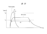
- FIG. 29 is a diagram showing the relationship between the pulse width and temperature necessary for the phase change of the resistive memory element using the phase change material.
- the vertical axis is temperature
- the horizontal axis is time.
- a set pulse is applied that keeps the memory element in a temperature range lower than the melting point Ta but higher than the crystallization temperature Tx (same as or higher than the glass transition temperature). To do. Thereby, the chalcogenide material is in a low-resistance polycrystalline state.
- the time t2 required for crystallization varies depending on the composition of the chalcogenide material.
- the temperature of the element shown in FIG. 29 depends on Joule heat generated by the memory element itself and thermal diffusion to the surroundings.
- Non-Patent Document 3 describes a phase change memory that requires about 120 ns for reducing the resistance of a chalcogenide material and about 50 ns for increasing the resistance.
- Patent Document 6 and Patent Document 7 disclose a nonvolatile memory having a three-dimensional structure.
- Patent Document 6 shows a configuration in which memory cells each including a variable resistance element and a transistor connected in parallel thereto are connected in series in the stacking direction.
- Patent Document 7 shows a configuration in which memory cells each including a variable resistance element and a diode connected in series to the variable resistance element are connected in series with a conductive wire interposed in the stacking direction.
- this configuration for example, by applying a potential difference between the conductive line between two memory cells and the two conductive lines outside the two memory cells, the two memory cells can be collectively processed. Then, a write operation is performed.
- JP 2008-146255 A Japanese Patent Application Laid-Open No. 07-153285 Japanese Patent No. 3926985 JP 2004-240572 A International Publication No. 2011/114503 International Publication No. 2011/0774545 JP 2011-142186 A
- the present inventors examined a method for controlling a NAND flash memory used for storage such as an SSD (Solid State Drive) or a memory card. Furthermore, the present inventors examined the resistance characteristic of a phase change memory using a recording layer made of a chalcogenide material and a diode. The details of the study are described below.
- the SSD is composed of a plurality of NAND flash memories and a controller that controls these flash memories.
- the host controller and the SSD are connected by, for example, a SATA (Serial Advanced Technology Attachment) interface.
- a write operation when a data write command for one page is issued from the host controller toward such an SSD will be described.
- Data is written to the NAND flash memory in units of pages, and data is written according to the following procedure.
- the controller reads data (135168 bytes) for one block from the NAND flash memory.
- the data in the memory area storing the data for one block (135168 bytes) is erased.
- one page of data (2112 bytes) is newly written in the memory area.
- the NAND flash memory has a maximum erasable number (ERASEmax).
- ERASEmax maximum number of erasable times
- NAND flash memory the data writing unit and the data erasing unit are greatly different.
- the NAND flash memory needs to erase 64 times the data size (135168 bytes) when writing one page of data (2112 bytes), and it can be said that the data erasing method is very inefficient.
- the life of the SSD using the NAND flash memory is likely to decrease.
- Patent Documents 1 to 4 various techniques for improving the lifetime are known.
- an effective writing time or the like may increase as control becomes complicated. is there.
- the write speed and the erase speed of the NAND flash memory are originally low, and the overhead associated with such complicated control is added. It is not easy to achieve both enlargement and high speed. Furthermore, when writing one page of data (2112 bytes), it is necessary to read this one block of data before erasing one block of data (135168 bytes), which further reduces the writing performance. There are also concerns.
- a resistance change type memory As a resistance change type memory, a phase change memory (Phase Change Memory), a ReRAM (Resistive RAM) and the like have been developed. When such a resistance change type memory is used, the writing speed can be greatly improved as compared with the case where a NAND flash memory is used.
- the resistance change type memory can overwrite data, and its minimum unit is as small as 1 byte. In other words, only the necessary data size can be rewritten.
- such a memory has an upper limit of the number of times of writing, and this upper limit determines the life of the resistance change memory. For this reason, for example, if writing to a specific memory cell is concentrated, the lifetime may be shortened.
- the required performance (speed, life, capacity) for the non-volatile memory may vary depending on the system using the non-volatile memory.
- the resistance change type memory has a higher writing speed than the NAND type flash memory and the minimum unit of rewriting is small. Therefore, these characteristics are used to balance performance such as speed, life and capacity. A control method to ensure well is required.
- writing into the phase change memory is performed by controlling the Joule heat generated by the current and thereby controlling the resistance value of the memory cell as described in FIG.
- the resistance value after the rewrite operation may vary due to the difference in the electrical characteristics of the memory cell caused by the thermal history due to the Joule heat.
- Joule heat generated in a certain memory cell affects the peripheral memory cell, so that the resistance value of the peripheral memory cell may vary.
- the variation amount of the resistance value of the memory cell may fluctuate depending on whether the write information or the storage information of the peripheral memory cell is set or reset. For example, when a simple writing method such as that of Patent Document 7 is used, such a variation problem may occur. Therefore, in order to ensure the required performance of the nonvolatile memory described above including optimization of the writing method. It is desirable to realize a control method.
- the semiconductor device controls a nonvolatile memory unit including a plurality of memory cells and a physical address assigned to an externally input logical address and accesses the physical address of the nonvolatile memory unit Circuit.
- the nonvolatile memory unit is disposed at intersections of the plurality of first signal lines, the plurality of second signal lines intersecting with the plurality of first signal lines, and the plurality of first signal lines and the plurality of second signal lines.
- Each of the plurality of memory cell groups includes first to Nth (N is an integer of 2 or more) memory cells and first to Nth memory cell selection lines for selecting the first to Nth memory cells, respectively.
- the control circuit in response to the first write command to the first physical address, writes data to the first part of M (M ⁇ N) in the first to Nth memory cells, and In response to a second write command to the first physical address that occurs after the write command, data is written into M second portions excluding the first portion in the first to Nth memory cells.
- FIG. 1 is a block diagram illustrating a schematic configuration example of an information processing system to which a semiconductor device according to an embodiment of the present invention is applied. It is a block diagram which shows the structural example of the control circuit in FIG.
- FIG. 2 is a block diagram illustrating a configuration example of a nonvolatile memory device in FIG. 1.
- FIG. 3B is a circuit diagram showing a configuration example of the chain memory array in FIG. 3A.
- FIG. 3C is an explanatory diagram showing an operation example of the chain memory array of FIG. 3B. It is explanatory drawing which shows another operation example of the chain memory array of FIG. 3B.
- FIG. 3B is an explanatory diagram showing an example of a schematic write operation timing in the nonvolatile memory device of FIG. 3A.
- FIG. 3B is an explanatory diagram showing an example of a schematic read operation timing in the nonvolatile memory device of FIG. 3A.
- FIG. 2 is a diagram illustrating an example of an initial sequence when power is turned on in the information processing system of FIG. 1. In the information processing system of FIG. 1, it is a figure which shows another example of the initial sequence at the time of power activation. It is a figure which shows the structural example of the physical address table stored in the random access memory of FIG. It is a figure which shows the structural example of the physical segment table stored in the random access memory of FIG. It is a figure which shows the other structural example of the physical segment table stored in the random access memory of FIG.
- FIG. 3 is a diagram illustrating a configuration example of a write physical address table stored in the control circuit of FIG.
- FIG. 3 is a diagram illustrating a configuration example of a write physical address table stored in the control circuit of FIG. 2 and the random access memory of FIG. 1.
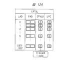
- FIG. 2 is a diagram illustrating a configuration example of an address conversion table stored in a random access memory in FIG. 1 and a state example after initial setting thereof.
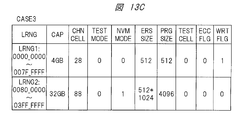
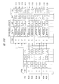
- FIG. 2 is a diagram illustrating an example of a state after initial setting in the nonvolatile memory device of FIG. 1. It is a figure which shows an example of the SSD configuration information stored in the non-volatile memory device for boot in FIG. It is a figure which shows another example of the SSD configuration information stored in the non-volatile memory device for boot in FIG. FIG.
- FIG. 7 is a diagram showing still another example of SSD configuration information stored in the bootable nonvolatile memory device in FIG. 1.
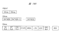
- FIG. 2 is a diagram showing a configuration example of data written from a control circuit to a nonvolatile memory device in the memory module of FIG. 1. It is a figure which shows the structural example of the data writing layer information in FIG. 14A. It is a figure which shows the structural example of the data writing layer information in FIG. 14A. It is a figure which shows an example of the address map range stored in the random access memory of FIG.
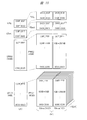
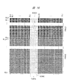
- FIG. 16 is a supplementary diagram of FIG. 15, schematically showing an arrangement example of writable memory cells set by the control circuit based on the SSD configuration information of FIG. 13A and the address map range of FIG. 15.
- FIG. 15 is a supplementary diagram showing still another example of SSD configuration information stored in the bootable nonvolatile memory device in FIG. 1.
- FIG. 4 is an explanatory diagram showing an example of a writing method to the chain memory array in the nonvolatile memory device of FIGS. 3A and 3B.
- FIG. 4 is an explanatory diagram showing another example of a writing method to the chain memory array in the nonvolatile memory device of FIGS. 3A and 3B.
- FIG. 10 is an explanatory diagram showing still another example of a writing method to the chain memory array in the nonvolatile memory device of FIGS. 3A and 3B.
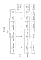
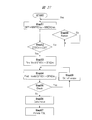
- FIG. 2 is a flowchart illustrating an example of a detailed write processing procedure performed in the memory module when a write request is input from the information processing apparatus of FIG. 1 to the memory module.
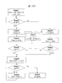
- FIG. 12 is a flowchart showing an example of the update method in the write physical address table of FIGS.
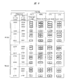
- FIG. 16 is a diagram illustrating an example of a correspondence relationship between a logical address, a physical address, and an in-chip address in the nonvolatile memory device assigned to the first physical address area in FIG. 15 and the like.
- FIG. 16 is a diagram illustrating an example of a correspondence relationship between a logical address, a physical address, and an in-chip address in the nonvolatile memory device assigned to the second physical address area in FIG. 15 and the like.
- FIG. 3 is a diagram illustrating an example of a change in physical address when the information processing circuit of FIG. 2 performs data writing or data reading to a nonvolatile memory device.
- FIG. 3 is a diagram illustrating an example of a change in physical address when the information processing circuit of FIG. 2 performs data writing or data reading to a nonvolatile memory device.
- FIG. 3 is a diagram illustrating an example of an address conversion table update method and a data update method of the nonvolatile memory device when the control circuit of FIG. 1 writes data to the first physical address area of the nonvolatile memory device. It is a figure which shows an example of the update method of the address conversion table following FIG. 23A, and the data update method of a non-volatile memory device.
- FIG. 3 is a diagram illustrating an example of an address conversion table update method and a data update method of the nonvolatile memory device when the control circuit of FIG. 1 writes data to the second physical address area of the nonvolatile memory device. It is a figure which shows an example of the update method of the address conversion table following FIG. 23A, and the data update method of a non-volatile memory device.
- FIG. 2 is a flowchart illustrating an example of a data read operation performed by a memory module when a read request is input from the information processing apparatus of FIG. 1 to the memory module.
- FIG. 14 is a flowchart illustrating an example of a write operation of a memory module according to write method selection information, using the SSD configuration information illustrated in FIG. 13B as an example.
- FIG. 22 is a flowchart showing an example of a wear leveling method executed by the information processing circuit of FIG. 2 in addition to the case of FIG.
- FIG. 3 is a diagram illustrating an example of a data write operation that is executed in a pipeline manner within the memory module when successive write requests are generated from the information processing apparatus of FIG. 1 to the memory module. It is a figure which shows the relationship between pulse width and temperature required for the phase change of the resistive memory element using a phase change material.
- the constituent elements are not necessarily indispensable unless otherwise specified or apparently indispensable in principle.
- the shapes when referring to the shapes, positional relationships, etc. of the components, etc., the shapes are substantially the same unless otherwise specified, or otherwise apparent in principle. And the like are included. The same applies to the above numbers and the like (including the number, numerical value, quantity, range, etc.).
- the circuit elements constituting each block are not particularly limited, but are formed on a single semiconductor substrate such as single crystal silicon by a known integrated circuit technology such as a CMOS (complementary MOS transistor). Further, a resistive memory element such as a phase change memory or a ReRAM (Resistive (Random Access Memory) is used for these memory cells.
- CMOS complementary MOS transistor
- a resistive memory element such as a phase change memory or a ReRAM (Resistive (Random Access Memory) is used for these memory cells.
- FIG. 1 is a block diagram showing a schematic configuration example of an information processing system to which a semiconductor device according to an embodiment of the present invention is applied.
- the information processing system shown in FIG. 1 includes an information processing device (processor) CPU_CP and a memory module (semiconductor device) NVMMD0.
- the information processing device CPU_CP is a host controller that manages data stored in the memory module NVMMD0 with a logical address (LAD) in units of a minimum of 512 bytes, although not particularly limited.
- the information processing device CPU_CP reads and writes data from and to the memory module NVMMD0 through the interface signal HDH_IF.
- the memory module NVMMD0 is not particularly limited, but corresponds to, for example, an SSD (Solid State Drive).
- the signal system for connecting the information processing device CPU_CP and the memory module (semiconductor device) NVMMD0 includes a serial interface signal system, a parallel interface signal system, and an optical interface signal system. Needless to say, all methods can be used.
- a clock system for operating the information processing device CPU_CP and the memory module NVMMD0 there are a common clock system and a source synchronous clock system using a reference clock signal REF_CLK, an embedded clock system in which clock information is embedded in a data signal, and the like. Needless to say, all clock systems can be used.
- a serial interface signal system and an embedded clock system are used as an example, and the operation will be described below.
- a read request (RQ), a write request (WQ) or the like embedded with clock information and converted into serial data is input to the memory module NVMMD0 through the interface signal HDH_IF.
- the read request (RQ) includes a logical address (LAD), a data read command (RD), a sector count (SEC), and the like
- the write request (WQ) includes a logical address (LAD) and a data write command (WRT). ), Sector count (SEC), write data (WDATA), and the like.
- the memory module (semiconductor device) NVMMD0 includes nonvolatile memory devices NVM10 to NVM17, a random access memory RAM, and a control circuit MDLCT0 that controls the nonvolatile memory device and the random access memory.
- the nonvolatile memory devices NVM10 to NVM17 have, for example, the same configuration and performance.
- the non-volatile memory device NVM10 stores data, OS, application program, SDD configuration information (SDCFG), and further stores a boot program for the information processing device CPU_CP and the like in .about.NVM17.
- the random access memory RAM is not particularly limited, but is a DRAM or the like, for example.
- the memory module NVMMD0 Immediately after the power is turned on, the memory module NVMMD0 performs an initialization operation (so-called power-on reset) of the internal nonvolatile memory devices NVM10 to NVM17, the random access memory RAM, and the control circuit MDLCT0. Further, the memory module NVMMD0 initializes the internal nonvolatile memory devices NVM10 to NVM17, the random access memory RAM, and the control circuit MDLCT0 when receiving the reset signal RSTSIG from the information processing device CPU_CP.
- an initialization operation so-called power-on reset
- the memory module NVMMD0 initializes the internal nonvolatile memory devices NVM10 to NVM17, the random access memory RAM, and the control circuit MDLCT0 when receiving the reset signal RSTSIG from the information processing device CPU_CP.
- FIG. 2 is a block diagram showing a configuration example of the control circuit in FIG.
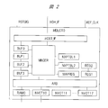
- the control circuit MDLCT0 shown in FIG. 2 includes an interface circuit HOST_IF, buffers BUF0 to BUF3, write physical address tables NXPTBL1 and NXPTBL2, an arbitration circuit ARB, an information processing circuit MNGER, memory control circuits RAMC and NVCT10 to NVCT17, A map register MAPREG and registers REG1 and REG2 are provided.
- the memory control circuit RAMC directly controls the random access memory RAM of FIG. 1, and the memory control circuits NVCT10 to NVCT17 directly control the nonvolatile memory devices NVM10 to NVM17 of FIG.
- Buffers BUF0 to BUF3 temporarily store write data and read data of nonvolatile memory devices NVM10 to NVM17.
- the write physical address tables NXPTBL1 and NXPTBL2 will be described in detail later with reference to FIG. 11 and the like.
- the physical address assigned to the logical address is The stored table is not particularly limited, and is realized by an SRAM, a register, or the like.
- the map register MAPREG and the registers REG1 and REG2, which will be described in detail later with reference to FIG. 13 and the like, are registers that hold information related to the entire area of the memory space.
- SDD configuration information (SDCFG) and the boot program are arranged in the control circuit MDLCT0, for example, directly connected to the information processing circuit MNGER in FIG. 2 in order to speed up the initial setting of the memory module NVMMD0. It is also possible.
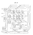
- 3A is a block diagram illustrating a configuration example of the nonvolatile memory device in FIG. 1
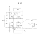
- FIG. 3B is a circuit diagram illustrating a configuration example of the chain memory array in FIG. 3A.
- the nonvolatile memory device shown in FIG. 3A corresponds to each of the nonvolatile memory devices NVM10 to NVM17 of FIG. 1, and here, as an example, a phase change type nonvolatile memory (phase change memory) is used. Yes.
- the nonvolatile memory device includes a clock generation circuit SYMD, a status register STREG, an erase size designation register NVREG, an address / command interface circuit ADCMDIF, an IO buffer IOBUF, a control circuit CTLOG, a temperature sensor THMO, a data control circuit DATCTL, and memory banks BK0 to BK3 is provided.
- the various peripheral circuits include a row address latch RADLT, a column address latch CADLT, a row decoder ROWDEC, a column decoder COLDEC, a chain selection address latch CHLT, a chain decoder CHDEC, a data selection circuit DSW1, and data buffers DBUF0 and DBUF1. .
- a bit line selection circuit BSWx that selects either one and connects to the data line DTx is provided.
- each chain memory array CY has a configuration in which a plurality of phase change memory cells CL0 to CLn are connected in series, one end of which is connected to a word line WL via a diode D, and the other end Are connected to the bit line BL via the chain selection transistor Tch.
- the plurality of phase change memory cells CL0 to CLn are stacked in the height direction with respect to the semiconductor substrate.
- Each phase change memory cell CL includes a variable resistance type storage element R and a memory cell selection transistor Tcl connected in parallel thereto.
- the memory element R is made of, for example, a chalcogenide material.
- the two chain memory arrays CY share the diode D, and the chain selection transistors Tch in each chain memory array are controlled by the chain memory array selection lines SL0 and SL1, respectively.
- One chain memory array is selected.
- the memory cell selection lines LY (LY0 to LYn) control the memory cell selection transistors Tcl in the phase change memory cells CL0 to CLn, respectively, thereby appropriately selecting each phase change memory cell.
- the chain memory array selection lines SL0 and SL1 and the memory cell selection lines LY0 to LYn are appropriately driven as the chain control line CH via the chain selection address latch CHLT and the chain decoder CHDEC in FIG.
- the control circuit CTLOG receives the control signal CTL via the address / command interface circuit ADCMDIF.
- the control signal CTL is not particularly limited.
- a write command or a read command is issued by a combination thereof including a ready busy signal (RBB).
- the control circuit CTLOG receives the input / output signal IO through the IO buffer IOBUF together with the control signal CTL.
- the input / output signal IO includes an address signal, and the control circuit CTLOG extracts a row address and a column address from the address signal.
- the control circuit CTLOG generates internal addresses as appropriate based on the row address, column address, and predetermined write / read unit, and transmits them to the row address latch RADLT, column address latch CADLT, and chain selection address latch CHLT, respectively. To do.
- the row decoder ROWDEC receives the output of the row address latch RADLT and selects the word lines WL0 to WLk
- the column decoder COLDEC receives the output of the column address latch CALLT and selects the bit lines BL0 to BLi.
- the chain decoder CHDEC receives the output of the chain selection address latch CHLT and selects the chain control line CH.
- the read data is amplified by the sense amplifiers SA0 to SAm and transmitted to the data buffer DBUF0 (or DBUF1) via the data selection circuit DSW1.
- the data on the data buffer DBUF0 (or DBUF1) is sequentially transmitted to the input / output signal IO via the data control circuit DATCTL and the IO buffer IOBUF.
- a write command is input by the control signal CTL
- a data signal is transmitted to the input / output signal IO following the address signal described above, and the data signal is transferred to the data buffer DBUF0 ( Or it is input to DBUF1).
- a data signal on the data buffer DBUF0 (or DBUF1) is selected by a combination of the above-described word line, bit line, and chain control line via the data selection circuit DSW1, write drivers WDR0 to WDRm, and bit line selection circuits BSW0 to BSWm. Is written to the chain memory array CY.
- the write data verification circuits WV0 to WVm verify whether or not the write level has reached a sufficient level while appropriately reading the written data through the sense amplifiers SA0 to SAm.
- the write operation is performed again using the write drivers WDR0 to WDRm until it reaches.
- FIG. 4 is an explanatory diagram showing an operation example of the chain memory array of FIG. 3B.
- an operation when the variable resistance memory element R0 in the phase change memory cell CL0 in the chain memory array CY1 is set to a high resistance or a low resistance will be described.
- the memory cell selection transistor Tcl0 of the phase change memory cell CL0 is cut off, and the remaining memory cells CL1 to CLn.
- the memory cell selection transistors Tcl1 to Tcln are turned on.
- the current I0 is supplied from the word line WL0 to the diode D0, the variable resistance storage element R0, the memory cell selection transistors Tcl1 to Tcln, and the chain selection transistor Tch1.
- the variable resistance memory element R0 has a high resistance.
- the current I0 is controlled in the form of the Set current pulse shown in FIG. 29, so that the variable resistance memory element R0 has a low resistance.
- Data “1” and “0” are distinguished by the difference in resistance value of the variable resistance memory elements R0 to Rn. Although not particularly limited, it is assumed that data “1” is recorded when the variable resistance memory element becomes low resistance, and data “0” is recorded when the variable resistance memory element becomes high resistance.
- a current is applied through the same path as the data writing so that the resistance value of the variable resistance memory element R0 does not change.
- a voltage value corresponding to the resistance value of the variable resistance storage element R0 is detected by a sense amplifier (SA0 in FIG. 3A in this example), and data “0” and “1” are determined.
- FIG. 5 is an explanatory diagram showing another operation example of the chain memory array of FIG. 3B.
- the current I1 is supplied from the word line WL0 through the diode D0, the variable resistance storage elements R0 to Rn, and the chain selection transistor Tch1. It flows to BL0.
- the variable resistance memory elements R0 to Rn collectively have a low resistance.
- FIGS. 17 to 19 are explanatory diagrams showing an example of a writing method to the chain memory array in the nonvolatile memory device of FIGS. 3A and 3B.
- the nonvolatile memory device according to the present embodiment applies to (n + 1) -bit phase change memory cells constituting a chain memory array in response to one write command from the host (CPU_CP in FIG. 1) side.
- a second operation mode for writing (n + 1) bits and a first operation mode for writing j bits (j ⁇ (n + 1)) are provided.
- the write operation in each operation mode will be described. Note that the detailed control method for the word line, bit line, chain control line, and the like accompanying the write operation is the same as in the case of FIGS.
- chain memory arrays CY0000 and CY0010 are assigned to the same physical address [1].
- the memory cell selection line LY0 is used.
- both memory cell selection lines “0” (reset state) is written for the phase change memory cell corresponding to LY0 (holding “1” with the initial write (erase) of the set state described above).
- the Reset current pulse of FIG. 29 is applied between the word line WL0 and the bit line BL0_0 and between the word line WL0 and the bit line BL0_1.
- the memory cell selection line LY1 is used this time.
- 1-bit data for the chain memory array CY0000 associated with the write instruction [2] is “1”
- 1-bit data for the chain memory array CY0010 is “0”.
- the data of the phase change memory cell corresponding to the memory cell selection line LY1 in the chain memory arrays CY0000 and CY0010 is “1” in advance with the initial writing (erasing) on the memory cell selection line LY0. .
- the Reset current pulse of FIG. 29 is applied between the word line WL0 and the bit line BL0_1. At this time, no current pulse is particularly applied between the word line WL0 and the bit line BL0_0.
- the chain memory arrays CYk001 and CYk011 are assigned to the same physical address [2].
- a state after a write command [n + 1] for the physical address [2] is input is shown.
- 1-bit data for the chain memory array CYk001 is “1”
- 1-bit data for the chain memory array CYk011 is “0”.
- initial write is performed once in response to the write command of n times, and then the memory cell selection lines are changed to LY0 ⁇ LY1 ⁇ ... LY (n ⁇ 1). While transitioning, “1” is written (however, write operations other than initial writing are not actually performed). Thereafter, in the chain memory array CYk011, “0” (reset state) is written to the phase change memory cell corresponding to the memory cell selection line LYn in response to the write command [n + 1] of the 1-bit data “0” described above. It is.
- FIG. 18 shows an example of a change in the chain memory array accompanying the write operation in the second operation mode described above.
- chain memory arrays CYk000 and CYk010 are assigned to the same physical address [1].
- a write command [1] for the physical address [1] is input, in the chain memory arrays CYk000 and CYk010, first, all the phase change memory cells in the first are temporarily set as “ 1 "(set state) writing (that is, the above-described initial writing (erasing)) is performed. Thereafter, predetermined data associated with the write command [1] is written to all the phase change memory cells in the chain memory arrays CYk000 and CYk010.
- the (n + 1) -bit data for the chain memory array CYk000 associated with the write instruction [1] is “0... 00”
- the (n + 1) -bit data for the chain memory array CYk010 is “0. It has become.
- the data of all the phase change memory cells in the chain memory arrays CYk000 and CYk010 is “1” in advance with the initial write (erase) described above. Therefore, in the phase change memory cell (here, the phase change memory cell corresponding to LY1 in CYk010) corresponding to the bit having the data “1” associated with the write command [1], the write operation is not performed. "0" (reset state) is written for the phase change memory cell.
- the memory cell selection lines to be deactivated are sequentially shifted as LY0 ⁇ LY1 ⁇ ... ⁇ LYn, and each time between the word line WLk and the bit line BL0_0, and between the word line WLk and the bit. It is selected whether or not to apply the Reset current pulse of FIG. 29 between the lines BL0_1.
- the Reset current pulse is applied when the area between the word line WLk and the bit line BL0_1 when the memory cell selection line LY1 is deactivated is removed.
- a reset current pulse is applied between the word line WLk and the bit line BL0_0 in a state where all the memory cell selection lines LY0 to LYn are inactive, and then the memory cell selection lines LY0 to LYn are set to LY1.
- a reset current pulse may be applied between the word line WLk and the bit line BL0_1 in a state where all of them are inactive.
- chain memory arrays CY0000 and CY0010 are assigned to the same physical address [1].
- a write command [1] targeted for the physical address [1] is input, first, in the chain memory arrays CY0000 and CY0010, two memory cell selection lines LY0 and LY1 are used.
- the initial write described above for all the phase change memory cells in the chain memory arrays CY0000 and CY0010 is performed. (Erase) is performed. Thereafter, predetermined data associated with the write command [1] is written to the phase change memory cells corresponding to the memory cell selection lines LY0 and LY1.
- the 2-bit data for the chain memory array CY0000 associated with the write command [1] is “00” and the 2-bit data for the chain memory array CY0010 is “10”.
- the memory cell selection line to be deactivated is shifted as LY0 ⁇ LY1, and each time between the word line WL0 and the bit line BL0_0 and between the word line WL0 and the bit line BL0_1, respectively. This is done by selecting whether or not to apply the Reset current pulse of FIG.
- the memory cell selection lines LY2 and LY3 are used this time.
- the case where the 2-bit data for the chain memory array CY0000 associated with the write instruction [2] is “11” and the 2-bit data for the chain memory array CY0010 is “10” is taken as an example.
- the state after such a write operation is shown in the chain memory arrays CY0000 and CY0010 of FIG.
- the memory cell selection lines to be used are changed from LY4, LY5 to LY6, LY7 to.
- the above-described initial writing (erasing) is performed again.
- the (n + 1) -bit chain memory array is used as having a storage capacity of j ( ⁇ (n + 1)) bits, and the j-bit is stored in the chain memory array. Since the control is performed so as to circulate, the speed can be increased and the life can be extended as compared with the second operation mode described above. That is, for example, in the case of FIG. 17, the maximum number of bits to be written in “0” (reset state) is reduced to 1 / (n + 1) as compared with the case of FIG. The maximum time required for writing, including the verify operation, can be shortened. Also, all the bits in the chain memory array are used once by (n + 1) write commands in the case of FIG. 17, whereas they are used once by one write command in the case of FIG. Therefore, in the case of FIG. 17, the lifetime is extended by about (n + 1) times compared to the case of FIG.
- the capacity and cost can be reduced compared to the first operation mode. That is, for example, in the case of FIG. 17, one chain memory array is used as having a storage capacity of 1 bit, whereas in FIG. 18, one chain memory array is (n + 1). ) Since it is used as having a bit storage capacity, the capacity value per unit area increases, and the bit cost can be set low. As a result, for example, by providing an area used in the first operation mode and an area used in the second operation mode in the nonvolatile memory device, by appropriately combining the first operation mode and the second operation mode, the speed can be increased. Thus, it is possible to ensure a good balance of performance such as life and capacity, and to flexibly cope with the performance required by the user.
- the set state is used at the time of initial writing (erasing), and the reset state is used at the time of writing to a specific memory cell thereafter.
- the set state is usually more stable than the reset state.
- the pulse width when writing the set state is wider than the pulse width when writing the reset state. Heat generation tends to spread to the periphery, which increases the possibility of affecting the storage state of the surrounding phase change memory cells. In view of these, it is beneficial to use a method that does not cause writing of a set state for a specific phase change memory cell as in the writing method of the present embodiment.
- the surrounding phase change memory cell is stable in the set state with initial writing (erasing), and Since the pulse width associated with writing in the reset state is narrow, the spread of heat associated with the writing is also suppressed.
- the present invention is not limited to this.
- the correspondence relationship can be changed as appropriate.
- n 3 and four phase change memory cells (for example, corresponding to CY0000) stacked in order, and four phase change stacked next to each other and sharing a diode and a bit line.
- a memory cell (for example, corresponding to CY0001) can be associated with one chain memory array.
- initial writing (erasing) of the chain memory array is performed in two steps by sequentially activating the chain memory array selection lines SL0 and SL1.
- the write current can be set to double
- the memory cell selection line is sequentially shifted every time a write command is input.
- the shift is not performed.
- Such a function can also be added.
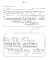
- FIG. 6 is an explanatory diagram showing an example of a schematic write operation timing in the nonvolatile memory device of FIG. 3A.
- NVM1x 0 to 7
- M bytes of data are transferred to the memory arrays ARY0 to ARY0 through the data buffer DBUF0.
- a case where data is written to a phase change memory cell in ARYm is taken as an example.
- “*” such as “m * n” in FIG. 6 means “x” (multiplication).
- the command latch enable signal CLE that is at low level is driven to high level, and the chip enable signal CEB and address latch enable signal ALE that are at high level are driven to low level.
- the write command W10 is shown by the rising edge of the write enable signal WEB.
- the data is taken into the address / command interface circuit ADCMDIF of 3A and decoded.
- the write command W10 also includes information for designating the data buffer DBUF0 or DBUF1, and the data buffer DBUF0 is designated in the example of FIG.
- the command latch enable signal CLE that is at a high level is driven to a low level
- the address latch enable signal ALE that is at a low level is driven to a high level
- the column address is set twice.
- CA1, CA2 and the row address are inputted in order by dividing into three times (RA1, RA2, RA3).
- These addresses are taken into the address / command interface circuit ADCMDIF by the rising edge of the write enable signal WEB and decoded.
- the control circuit CTLOG if the control circuit CTLOG is informed that it is a write command to the memory bank BK0, the control circuit CTLOG writes data to the memory bank BK0. Then, the memory bank BK0 is activated.
- the chain address (CHAD) and the cell address (CLAD) are transferred from the chain selection address latch CHLT to the chain decoder CHDEC, and the chain memory array corresponding to the chain address (CHAD) and the cell address (CLAD) by the chain decoder CHDEC.
- Select line SL and memory cell select line LY are selected.
- the column address (CA1, CA2) is transferred from the column address latch CALLT to the column decoder COLDEC and decoded.
- the write drivers WDR0 to WDRm set the bit line BLi_x selected via the data lines DT0 to DTm to the Low state, and the phase change memory cell CL can be changed as shown in FIGS.
- the variable resistance memory element R is brought into a low resistance state or a high resistance state.
- variable resistance memory element R of the phase change memory cell CL When the variable resistance memory element R of the phase change memory cell CL is set to the low resistance state, that is, when the memory information “1” is written, the memory cell current Icl applied via the data lines DT0 to DTm is necessary for the set operation. It is controlled to a correct value (Iset). When the phase change memory cell CL is brought into a high resistance state, that is, when the memory information “0” is written, the memory cell current Icl applied via the data lines DT0 to DTm is controlled to a value (Ireset) necessary for the reset operation. Is done.
- the address latch enable signal ALE which is at the high level is driven to the low level, and the stored information DI (1), DI (2),... Is synchronized with the rising edge of the write enable signal WEB.
- Each storage information DI (1), DI (2),..., DI (M) is sequentially input to the data buffer DBUF0.
- n bytes of data are input to the data buffer DBUF0, n bytes of data are written through the n ⁇ 8 write drivers WDR. The operation is shown below.
- the phase change memory cell corresponding to the data “0” among the data held in the data buffer DBUF0 is replaced with the write driver.
- a high resistance state (program: PROG0 (1)) is written through WDR.
- the data writing operation for the third n bytes is performed in the same manner as the above operation, and the column address at that time is ⁇ CA1, CA2 ⁇ + (2n) ⁇ .
- a column address is generated while sequentially adding multiples of n to the start column address ⁇ CA1, CA2 ⁇ , and erased each time n bytes of phase change memory cells CL are selected by the column address.
- (ERS1), program (PROG0), and verify (VRF0) are executed.
- the addition of the column address is performed by, for example, the control circuit CTLOG in FIG. 3A.
- the write execution command W11 is on the instruction format for instructing the memory array to perform the actual write operation after the input of the storage information DI (1) to DI (M). It is a command. However, in the example of FIG. 6, before the write execution command W11 is received, an actual write operation is performed every time a predetermined amount of data is stored in the data buffer, thereby speeding up.
- M-byte writing in the second operation mode activates one bit line for each memory array ARY0 to ARYm, for example, for one word line, and thereby ARY0 to ARYm Is performed by selecting one chain memory array CY from each and selecting all memory cells in the CY as write targets. If the memory array configuration is assumed, M-byte writing in the first operation mode is performed by, for example, sequentially activating a plurality of word lines for one bit line for each of the memory arrays ARY0 to ARYm. Thus, a plurality of chain memory arrays CY are selected from ARY0 to ARYm, and one memory cell in the CY is set as a write target.
- a plurality of bit lines are sequentially activated for each memory array ARY0 to ARYm for one word line, thereby selecting a plurality of chain memory arrays CY from ARY0 to ARYm, This is performed by setting one memory cell in the CY as a write target.
- the phase change memory cell CL is temporarily erased without being overwritten, so that the resistance value of the phase change memory cell is made uniform. And a stable write operation can be realized. Furthermore, high reliability can be maintained by performing verification (VRF0) after programming (PROG0).
- FIG. 7 is an explanatory diagram showing an example of a schematic read operation timing in the nonvolatile memory device of FIG. 3A.
- data for the specified data size is stored in the memory arrays ARY0 to ARYm.
- “*” such as “k * n” in FIG. 7 means “x” (multiplication).
- the command latch enable signal CLE that is at low level is driven to high level, and the chip enable signal CEB and address latch enable signal ALE that are at high level are driven to low level.
- the first command is generated by the rising edge of the write enable signal WEB.
- Read command RD4 is taken into address / command interface circuit ADCOMIF and decoded.
- the command latch enable signal CLE that is at a high level is driven to a low level
- the address latch enable signal ALE that is at a low level is driven to a high level
- the column address is set twice.
- CA1, CA2 and the row address are inputted in order by dividing into three times (RA1, RA2, RA3). These addresses are taken into the address / command interface circuit ADCOMIF by the rising edge of the write enable signal WEB and decoded.
- the command latch enable signal CLE that is at the low level is driven to the high level, and the chip enable signal CEB and the address latch enable signal ALE that are at the high level are driven to the low level.
- the second read command RD41 is changed by the rising edge of the write enable signal WEB. Imported into ADCOMIF and decrypted.
- the commands RD4 and RD41 also include information for designating the data buffer DBUF0 or DBUF1, and the data buffer DBUF0 is designated in the example of FIG.
- the control circuit CTLOG when the control circuit CTLOG is informed that it is a read command to the memory bank BK0, the control circuit CTLOG receives data from the memory bank BK0. In order to read data, the memory bank BK0 is activated.
- the row address (RA1, RA2, RA3) and the column address (CA1, CA2) input to the address / command interface circuit ADCOMIF are sent through the control circuit CTLOG to the row address latch RADLT and the column of the activated memory bank BK0, respectively. Transferred to address latch CADLT and chain selection address latch CHLT. Here, the read operation is started from the column address input first.
- the chain address (CHAD) and the cell address (CLAD) are transferred from the chain selection address latch CHLT to the chain decoder CHDEC, and the chain memory array corresponding to the chain address (CHAD) and the cell address (CLAD) by the chain decoder CHDEC.
- Select line SL and memory cell select line LY are selected.
- the column address (CA1, CA2) is transferred from the column address latch CALLT to the column decoder COLDEC and decoded.
- the memory state A voltage corresponding to is generated.
- a predetermined phase change memory cell CL in the chain memory array CY located at the intersection of the word line WL0 and the bit line BL0_0 stores data “1” and is in a low resistance state
- the bit line BL0_0 and the data line DT0 are charged, and the sense amplifier SA0 detects data “1” from the voltages.
- the memory array ARY1 when a predetermined phase change memory cell CL in the chain memory array CY located at the intersection of the word line WL0 and the bit line BL0_1 stores data “0” and is in a high resistance state
- the bit line BL0_1 and the data line DT1 are substantially held at the ground voltage VSS, and the sense amplifier SA1 detects data “0” from the voltages.
- the next n bytes of data are selected by the column address ⁇ CA1, CA2 ⁇ + (n) ⁇ and transferred to the data buffer DBUF0.
- a column address is selected while sequentially adding multiples of n to the start column address ⁇ CA1, CA2 ⁇ , and n bytes of data are received from the phase change memory cell CL corresponding to the selected column address. Read out and sequentially transferred to the data buffer DBUF0.
- the addition of multiples of n is performed by, for example, the control circuit CTLOG in FIG. 3A.
- the designated data size is k * n bytes, data transfer from the memory array ARY to the data buffer DBUF0 occurs k times.
- the ready / busy signal RBB that is at the high level is at the low level.
- the ready / busy signal RBB which is at low level becomes high level.
- the input / output signal IO is 8 bits (1 byte)
- k * n bytes of data stored in the data buffer DBUF0 are synchronized with the falling edge of the read enable signal REB. It is output in the order of DO (1) to DO (k * n) via IO.
- the designated data size is 512 bytes
- the data size of the phase change memory cell CL selected at the same time is 16 bytes
- the input / output signal IO is 8 bits (1 byte)
- data is transferred from the phase change memory cell CL.
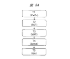
- FIG. 8A and 8B are diagrams showing examples of different initial sequences when the power is turned on in the information processing system of FIG.
- FIG. 8A shows an initial sequence at power-on when the SDD configuration information (SDCFG) stored in the nonvolatile memory devices NVM10 to NVM17 in the memory module (semiconductor device) NVMMD0 of FIG. 1 is used. is there.
- FIG. 8B shows an initial sequence when the power is turned on when the SDD configuration information (SDCFG) transmitted from the information processing device CPU_CP of FIG. 1 is used.
- the information processing device CPU_CP, the nonvolatile memory devices NVM10 to NVM17 in the memory module NVMMD0, the random access memory RAM, and the control circuit MDLCT0 are powered on in the period T1 (PwOn), and reset in the period T2 (RST) I do.
- the reset method is not particularly limited. For example, a method of automatically resetting by each built-in circuit or a method of having a reset terminal (reset signal RSTSIG) outside and performing a reset operation by this reset signal may be used. Alternatively, for example, a reset command may be input from the information processing device CPU_CP through the interface signal HDH_IF to the control circuit MDLCT0 to perform a reset.
- the control circuit MDLCT0 In the reset period (RST) of T2, the internal states of the information processing device CPU_CP, the control circuit MDLCT0, the nonvolatile memory devices NVM10 to NVM17, and the random access memory RAM are initialized. At this time, the control circuit MDLCT0 initializes an address range map (ADMAP) and various tables stored in the random access memory RAM.
- the various tables include an address conversion table (LPTBL), a physical segment table (PSEGTBL1, PSEGTBL2), a physical address table (PADTBL), and a write physical address table (NXPADTBL).
- the address range map (ADMAP) and various tables will be described in detail later, but will be briefly described as follows.
- the address range map (ADMAP) indicates partitioning of the address area used in the first operation mode and the address area used in the second operation mode.
- the address translation table (LPTBL) indicates the correspondence between the current logical address and physical address.
- the physical segment tables (PSEGTBL1, PSEGTBL2) manage the number of erasures at each physical address in units of segments and are used for wear leveling and the like.
- the physical address table (PADTBL) manages the current state of each physical address in detail.
- the write physical address table (NXPADTBL) defines a physical address to be assigned next to a logical address based on wear leveling.
- the write physical address table (NXPADTBL) is partially or entirely copied to the write physical address tables NXPTBL1 and NXPTBL2 shown in FIG. 2 in order to increase the write speed.
- the control circuit MDLCT0 reads the SDD configuration information (SDCFG) stored in the nonvolatile memories NVM10 to NVM17 and transfers it to the map register MAPREG in FIG. To do.
- the SSD configuration information (SDCFG) in the map register MAPREG is read, and the address range map (ADMAP) is generated using the SSD configuration information (SDCFG) and stored in the random access memory RAM.
- the SDD configuration information (SDCFG) includes information on the address area used in the first operation mode and the address area used in the second operation mode.
- the control circuit MDLCT0 writes the write physical address table (NXPADTBL) corresponding thereto. ) Build.
- NXPADTBL write physical address table
- the logical address area (LRNG1) corresponds to the area for the first operation mode described above
- the logical address area (LRNG2) corresponds to the area for the second operation mode described above.
- the write physical address table (NXPADTBL) is composed of N entries from the 0th entry to the (N-1) th entry, the (N / 2-1) entry from the 0th entry
- the N / 2 pieces up to the eye can be used as the write physical address table NXPADTBL1.
- the N / 2 entries from the remaining N / 2 entries to the N entries can be used as the write physical address table (NXPADTBL2).
- the information processing device CPU_CP reads the boot program stored in the nonvolatile memory device NVM0 in the memory module NVMMD0 and starts up the information processing device CPU_CP.
- the memory module NVMMD0 enters an idle state and waits for a request from the information processing device CPU_CP.
- the initial sequence shown in FIG. 8B will be described.
- the period T11 PwOn
- the period T21 RST
- operations similar to those in the periods T1 and T2 in FIG. 8A are performed, respectively.
- the information processing device CPU_CP transmits the SSD configuration information (SDCFG) to the memory module NVMMD0, and the control circuit MDLCT0 that receives the information transmits the SSD configuration information.
- Information (SDCFG) is stored in nonvolatile memory devices NVM10 to NVM17.
- the period T41 MAP
- the period T51 SetUp
- the period T61 Idle
- FIG. 9 is a diagram showing a configuration example of a physical address table stored in the random access memory of FIG.
- the physical address table PADTBL includes a physical address PAD (PAD [31: 0]), a valid flag PVLD corresponding to each physical address PAD, the number of times of erasing PERC, a layer mode number LYM, and a layer number LYC. It is stored in random access memory RAM.
- a valid flag PVLD value of 1 indicates that the corresponding physical address PAD is valid, and a valid flag PVLD value of 0 indicates that it is invalid.
- the valid flag PVLD value of the physical address PAD assigned after the change becomes 1, and the physical assigned before the change
- the valid flag PVLD value of the address PAD becomes 0.
- Erase count PERC represents the number of times the above-described initial writing (erasing) has been performed.
- a physical address PAD having a valid flag PVLD value of 0 and a small number of times of initial writing (erasing) is preferentially assigned to a logical address
- the value of the number of times of erasing PERC is equalized (ware Leveling).
- the information processing circuit MNGER in FIG. 2 uses the physical address PAD from “00000000” to “027FFFFF” as the first physical address area PRNG1, and the physical address PAD from “02800000” to “07FFFFFF”. Is managed as the second physical address area PRNG2 and the physical address table PADTBL is managed.
- the physical address PAD (PAD [31: 0]) includes a physical segment address SGAD (PAD [31:16]) and a segment-specific physical offset address PPAD (PAD [15: 0]). Consists of
- the layer mode number LYM When the layer mode number LYM is “0”, it indicates that writing is performed to all the phase change memory cells CL0 to CLn in the chain memory array CY (that is, the second operation mode described above). . When the layer mode number LYM is “1”, it indicates that writing is performed to one phase change memory cell in the chain memory array CY (that is, the first operation mode described above).
- the value x of the layer number LYC corresponds to the memory cell selection line LYx in the chain memory array CY shown in FIG.
- the layer number LYC is “1”
- the data corresponding to the physical address PAD is held in the phase change memory cell CL1 selected by the memory cell selection line LY1 in the chain memory array CY shown in FIG. Indicates that it is valid.
- FIG. 10A and FIG. 10B are diagrams showing a configuration example of a physical segment table stored in the random access memory of FIG.
- FIG. 10A shows the physical segment table PSEGTBL1 related to the invalid physical address
- FIG. 10B shows the physical segment table PSEGTBL2 related to the valid physical address.
- the upper PAD [31:16] of the physical address PAD indicates the physical segment address SGAD.
- the main data size of one physical address is 512 bytes, and the main data size of one segment is 32 Mbytes by collecting 65536 physical addresses.
- the physical segment table PSEGTBL1 includes, for each physical segment address SGAD (PAD [31:16]), the total invalid physical address TNIPA, the maximum erase count MXERC and the corresponding invalid physical offset address MXIPAD, the minimum erase count MNERC, and the corresponding And an invalid physical offset address MNIPAD.
- the total number of invalid physical addresses TNIPA is the total number of physical addresses that are in an invalid state in the corresponding physical segment address SGAD.
- the address MNIPAD is extracted from the invalid physical address.
- the physical segment table PSEGTBL1 is stored in the random access memory RAM of FIG.
- the physical segment table PSEGTBL2 includes, for each physical segment address SGAD (PAD [31:16]), the total effective physical address TNVPA, the maximum erase count MXERC and the corresponding valid physical offset address MXVPAD, the minimum erase count MNERRC, and the corresponding Effective physical offset address MNVPAD to be included.
- the total number of valid physical addresses TNVPA is the total number of valid physical addresses in the corresponding physical segment address SGAD.
- the address MNVPAD is extracted from the valid physical addresses.
- the physical segment table PSEGTBL2 is stored in the random access memory RAM of FIG.
- the physical segment tables PSEGTBL1 and PSEGTBL2 are used when performing dynamic wear leveling or static wear leveling described later.
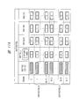
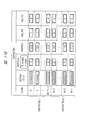
- FIG. 11A and FIG. 11B are diagrams showing a configuration example of a write physical address table stored in the control circuit of FIG. 2 and the random access memory of FIG.
- FIG. 11A shows the state of the write physical address table NXPADTBL in the initial state at the start of use of the apparatus
- FIG. 11B shows the state of the write physical address table NXPADTBL after the contents are appropriately updated.
- the write physical address table NXPADTBL receives a write command with a logical address from the host (CPU_CP in FIG. 1) and writes data to the physical addresses of the nonvolatile memory devices NVM10 to NVM17. It is a table which determines whether a physical address is preferentially assigned.
- the write physical address table NXPADTBL has a configuration in which a plurality (N) of physical addresses can be registered here.
- the write physical address table NXPADTBL (NXPADTBL1, NXPADTBL2) determines the physical address to be actually written, and the time from the reception of the logical address to the determination of the physical address using the table is as follows. Will affect the writing speed. Therefore, the information of the write physical address table NXPADTBL (NXPADTBL1, NXPADTBL2) is held in the write physical address tables NXPTBL1, NXPTBL2 in the control circuit MDLCT0 in FIG. 2, and is held as a backup in the random access memory RAM in FIG.
- the write physical address table NXPADTBL (NXPADTBL1, NXPADTBL2) determines the physical address to be actually written, and the time from the reception of the logical address to the determination of the physical address using the table is as follows. Will affect the writing speed. Therefore, the information of the write physical address table NXPADTBL (N
- the write physical address table NXPADTBL is composed of an entry number ENUM, a write physical address NXPAD, a valid flag NXPVLD corresponding to the write physical address NXPAD, an erase count NXPERC, a layer mode number NXLYM, and a write layer number NXLYC.
- the control circuit MDLCT0 in FIG. 2 has two logical address areas (LRNG1 and LRNG2) defined in the SSD configuration information (SDCFG), and 2 in the write physical address table NXPADTBL corresponding to this. Divide into pieces.
- N / 2 entries from entry numbers 0 to (N / 2-1) are managed as the write physical address table NXPADTBL1, and the remaining N / 2 from entry numbers (N / 2) to (N-1).
- the write physical address table NXPADTBL1 is used for a write request to the logical address area (LRNG1), and the write physical address table NXPADTBL2 is used for a write request to the logical address area (LRNG2). .
- the entry number ENUM indicates an N value (0th to (N-1)) in a plurality (N) sets of write physical addresses NXPAD, and this N value indicates a write priority (number of registrations).
- N value in the write physical address table NXPADTBL1 is used with priority from the smallest order, and write requests to the logical address area (LRNG2) are written.
- the N values in the physical address table NXPADTBL2 are used preferentially in ascending order. Further, when the value of the valid flag NXPVLD is 0, it means that the target physical address is invalid, and when it is 1, it means that the target physical address is valid.
- the value of the 0th validity flag NXPVLD is 1, so that the entry number ENUM 0 is already used when the table is referenced next time. It can be determined that it is sufficient to use No. 1 next time.
- a physical address area PRNG1 is set corresponding to the logical address area (LRNG1), and continuous write physical addresses NXPAD from the address “00000000” to the address “0000000F” in the physical address area (PRNG1) are
- the entry numbers ENUM 0 to ((32/2) -1) are registered respectively.
- the layer mode number NXLYM is set to “1”
- the write layer number NXLYC is set to “0”. This is the same as the layer mode number LYM and the layer number LYC described in FIG. This means that the memory cell selection line to be used is LY0.
- a physical address area PRNG2
- LRNG2 logical address area
- continuous write physical addresses NXPAD from the address “02800000” to the address “0280000F” in the physical address area (PRNG2) are set.
- the entry numbers ENUM (32/2) to (32-1) are registered respectively.
- the layer mode number NXLYM is set to “0”, and the write layer number NXLYC is set to “0”. This is the same as the layer mode number LYM and the layer number LYC described in FIG. Means mode.
- the valid flag NXPVLD and the erase count NXPERC corresponding to these write physical addresses NXPAD are all set to 0.
- the sector count (SEC) value is 1 (512 bytes) from the information processing device CPU_CP to the logical address area (LRNG1) of the memory module (semiconductor device) NVMMD0 through the interface signal HDH_IF.
- the write request (WQ) is input (N / 2) times.
- the data included in each write request (WQ) is stored in consecutive addresses from “00000000” to “000000F” of the physical address PAD (NXPAD) in the nonvolatile memory device based on FIG. 11A. Written in the corresponding location.
- a write request (WQ) having a sector count (SEC) value of 1 (512 bytes) is input (N / 2) times from the information processing device CPU_CP to the logical address area (LRNG2) of the memory module NVMMD0 through the interface signal HDH_IF.
- SEC sector count
- LRNG2 logical address area
- the data included in each write request (WQ) is stored in consecutive addresses from “02800000” to “0280000F” of the physical address PAD (NXPAD) in the nonvolatile memory device based on FIG. 11A. Written in the corresponding location.
- WQ write request
- SEC sector count
- LRNG1 logical address area
- the write physical address table NXPADTBL is appropriately updated.
- values such as the write physical address NXPAD, the number of erasures NXPERC, and the write layer number NXLYC are appropriately changed. Is done.
- the value of the write layer number NXLYC in the write physical address table NXPADTBL1 is changed accordingly because the memory cell selection line LY is sequentially shifted in accordance with the first operation mode described in FIG.
- the value of the write layer number NXLYC in the write physical address table NXPADTBL2 is not particularly changed according to the second operation mode described in FIG.
- the write physical address table NXPADTBL can be updated using, for example, a period during which data is actually written to the phase change memory cell in the memory array.
- FIG. 12A is a diagram showing a configuration example of the address conversion table stored in the random access memory of FIG. 1 and a state example after the initial setting
- FIG. 12B is a diagram after the initial setting in the nonvolatile memory device of FIG. It is a figure which shows an example of a state.
- the initial setting is performed, for example, by the control circuit MDLCT0 during the period T1 (immediately after power-on) in FIG.
- the address conversion table LPTBL shown in FIG. 12A is for all logical addresses LAD, and for each logical address LAD, currently assigned physical address PAD, valid flag CPVLD of the physical address, and layer number of the physical address LYC is managed. After the initial setting, all physical addresses PAD for all logical addresses LAD are set to 0, valid flag CPVLD is set to 0 (invalid), and layer number LYC is set to “0”. As shown in FIG. 12B, in the nonvolatile memory devices NVM10 to NVM17, the data DATA stored in each physical address PAD is set to 0, and the logical address LAD and the data valid flag DVF corresponding to each physical address PAD are also set. Set to zero. The layer number LYC corresponding to each physical address PAD is set to “0”. The logical address LAD, the data valid flag DVF, and the layer number LYC are stored using a redundant area provided in advance in the nonvolatile memory device, for example.
- LRNG is a logical address area, which indicates a range of logical addresses LAD in sector units (512 bytes).
- CAP indicates a capacity value of logical data in a range defined by the logical address area LRNG.
- the logical address area LRNG1 occupies a logical address LAD space of “0000_0000” to “007F_FFFF” in hexadecimal and has a capacity of 4 Gbytes.
- the logical address area LRNG2 occupies a logical address space of “0080_0000” to “037F_FFFF” in hexadecimal and has a size of 32 Gbytes.
- CHNCELL in the figure indicates the number of memory cells to which data is to be written among all the phase change memory cells CL0 to CLn in the chain memory array CY shown in FIG. 3B, for example. For example, as shown in FIGS. 13A and 13B, if CHNCELL is “18”, it indicates that writing is performed to “1” of “8” memory cells in the chain memory array CY. , CHNCELL is “88”, it indicates that writing is performed to “8” of “8” memory cells in the chain memory array CY. For example, as shown in FIG. 13C, if CHNCELL is “28”, it indicates that writing is performed to “2” of “8” memory cells in the chain memory array CY.
- NVMMODE in the figure is “0”, it indicates that the write operation can be performed with the minimum erase data size and the minimum program data size equal when writing data to the nonvolatile memory device NVM. In the case of 1 ′′, it indicates that the write operation can be performed on the assumption that the minimum erase data size and the minimum program data size are different.
- ERSSIZE indicates the minimum erase data size [bytes]
- PRGSIZE indicates the minimum program data size [bytes].
- NVMMODE is set to “0”, and the minimum erase data size (ERSSIZE) and the minimum program data size (PRGSIZE) are set. Both are of equal size, such as 512 bytes. In this case, the write operation can be performed at high speed.
- NVMMODE is set to “1” as shown in FIG. 13C.
- the minimum erase data size (ERSSIZE) is set to 512 kilobytes
- the minimum program data size (PRGSIZE) is set to 4 kilobytes, thereby writing to the conventional NAND flash memory.
- SDSIZE erase data size
- PRGSIZE minimum program data size
- TESTMODE in the figure is “1”
- a test operation for confirming the retention performance of data stored in physically adjacent memory cells is performed immediately after power-on.
- This test operation is performed using a test area (TESTAREA) that is prepared in advance to perform this test and includes a plurality of physically adjacent chain memory arrays CY. The test operation will be described below.
- the plurality of physically adjacent chain memory arrays CY in the test area is not particularly limited, and there are 25 (5 chains ⁇ 5 chains), and CY [1,1] to CY [5,5] have [[ X, Y] array.
- the variable resistance memory elements R of all the phase change memory cells in the 25 chain memory arrays CY [1,1] to CY [5,5] are put into a high resistance state ("0" is written).
- To a low resistance state write “1”).
- the same operation is performed with “0” and “1” reversed. That is, while “1” is written in the 25 chain memory arrays CY [1,1] to CY [5,5], “0” is written in the middle one chain memory array CY [3,3]. Then, the data of the peripheral chain memory array CY is read. Note that the number of the physically adjacent chain memory arrays CY in the test area (TESTAREA) is not limited to this value, but may be any value suitable for confirming the data holding performance. good.
- TESTCELL information is information necessary for determining a continuous memory cell area (TAAREA) for performing testing.
- TAREA continuous memory cell area
- the value of the TESTCELL information may be programmed to a value suitable for confirming the data holding performance.
- ECCCFLG in the figure indicates a data unit when performing ECC (Error Check and Correct).
- ECC Error Check and Correct
- ECC Error Check and Correct
- ECC Error Check and Correct
- ECC Error Check and Correct
- a hard disk such as a hard disk or an SSD
- reading and writing are performed in units of data of 512 bytes or more.
- the cache memory data is read from and written to the main memory in line size units (32 bytes, 64 bytes, etc.).
- ECC can be performed in different data units by ECCFLG, and the request to the memory module (semiconductor device) NVMMD0 can be flexibly handled.
- the write method selection information WRTFLG in the figure indicates a write method at the time of writing.
- writing is performed by the normal method
- WRTFLG is 1
- the inverted data is written
- the write method selection information WRTFLG is 2
- the write method selection information WRTFLG is 2
- SSD configuration information SDCFG
- SDCFG SSD configuration information
- ⁇ Configuration example of write data> 14A is a diagram showing a configuration example of data written from the control circuit MDLCT0 to the nonvolatile memory devices NVM10 to NVM17 in the memory module NVMMD0 of FIG. 14B and 14C are diagrams illustrating a configuration example of the data writing layer information in FIG. 14A.
- the write data (page data) PGDAT is composed of main data DArea (512 bytes) and redundant data RArea (16 bytes), although not particularly limited.
- the redundant data RArea includes a data inversion flag INVFLG, a write flag WTFLG, an ECC flag ECCFLG, state information STATE, area information AREA, data write layer information LYN, ECC code ECC, bad block information BADBLK, and a spare area RSV.
- the data inversion flag INVFLG indicates whether or not the main data DArea written by the control circuit MDLCT0 to the nonvolatile memory devices NVM10 to NVM17 is data obtained by inverting each bit of the original write data.
- 0 is written to the data inversion flag INVFLG, it indicates that the data has been written without inverting each bit of the original main data.
- 1 is written, each bit of the original main data is inverted. Indicates that the data has been written.
- the write flag WTFLG indicates the writing method executed when the control circuit MDLCT0 writes the main data DArea to the nonvolatile memory devices NVM10 to NVM17.
- 0 when 0 is written to WTFLG, it indicates that main data DArea has been written by a normal method, and when 1 is written to WTFLG, data obtained by inverting each bit of the original main data Indicates that has been written.
- 2 When 2 is written to WTFLG, it indicates that the data is once read before the data is written, and then only the data that needs to be rewritten is written.
- the ECC flag ECCFLG indicates how much the size of the main data DArea is generated when the control circuit MDLCT0 writes the main data DArea to the nonvolatile memory devices NVM10 to NVM17.
- 0 when 0 is written to ECCFLG, it indicates that a code is generated for a data size of 512 bytes.
- 1 When 1 is written to ECCFLG, a code is generated for a data size of 1024 bytes.
- the ECC code ECC is data necessary for detecting and correcting an error in the main data DArea.
- the ECC is generated by the control circuit MDLCT0 corresponding to the main data DArea when the control circuit MDLCT0 writes the main data DArea to the nonvolatile memory devices NVM10 to NVM17, and is written into the redundant data RArea.
- the state information STATE indicates whether the main data DArea written to the nonvolatile memory devices NVM10 to NVM17 is valid, invalid, or erased. Although not particularly limited, when 0 is written in the state information STATE, the main data DArea is in an invalid state, and when 1 is written in the state information STATE, the main data DArea is in a valid state. When 3 is written in the state information STATE, it indicates that the main data DArea is in the erased state.
- the area information AREA the data in which the main data DArea is written in the first physical address area PRNG1 or the second physical address area PRNG2 in the address map range (ADMAP) shown in FIG. This is information indicating whether data has been written.
- the area information AREA value is 1, it indicates that the main data DArea has been written to the first physical address area PRNG1, and if the area information AREA value is 2, the main data DArea is the second physical address. Indicates that data has been written to the address area PRNG2.
- the data write layer information LYN [n: 0] indicates which memory cell data is effectively written in the phase change memory cells CL0 to CLn in the chain memory array CY. It is information which shows. In the initial setting, LYN [n: 0] is set to zero. In this example, the case where the chain memory array CY includes eight phase change memory cells CL0 to CL7 is shown.
- the data write layer information LYN is composed of 8 bits LYN [7: 0], and LYN [7] to LYN [0] correspond to the phase change memory cells CL7 to CL0, respectively. For example, when valid data is written to the phase change memory cell CL0, “1” is written to LYN [0], and “0” is written otherwise. For example, when valid data is written in the phase change memory cell CL1, “1” is written in LYN [1], and “0” is written otherwise. The same applies to the relationship between the phase change memory cells CL2 to CL7 and LYN [2] to LYN [7].
- phase change memory cell CL0 of chain memory array CY In the example of FIG. 14B, since “1” is written to LYN [0] and “0” is written to LYN [7: 1], valid data is stored in phase change memory cell CL0 of chain memory array CY. Indicates that it has been written. In the example of FIG. 14C, “1” is written to LYN [0] and LYN [4], and “0” is written to LYN [7: 5] and LYN [3: 1]. It shows that valid data has been written to phase change memory cells CL0 and CL4 of CY.
- bad block information BADBLK indicates whether or not the main data DArea written in the nonvolatile memory devices NVM10 to NVM17 can be used. Although not particularly limited, when 0 is written in the bad block information BADBLK, the main data DArea is usable, and when 1 is written, the main data DArea is unusable. For example, when error correction by ECC is possible, bad block information BADBLK is 0, and when error correction is impossible, bad block information BADBLK is 1.
- the spare area RSV exists as an area that can be freely defined by the control circuit MDLCT0.
- FIG. 15 is a diagram showing an example of an address map range (ADMAP) stored in the random access memory of FIG.
- the address map range (ADMAP) is generated by the control circuit MDLCT0 using, for example, the SSD configuration information (SDCFG) shown in FIG. 13A stored in the NVM10 to NVM17 as described in FIG. It is stored in the random access memory RAM.
- SDCFG SSD configuration information
- FIG. 16 is a supplementary diagram of FIG. 15, and schematically shows an example of the arrangement of writable memory cells set by the control circuit MDLCT0 based on the SSD configuration information of FIG. 13A and the address map range (ADMAP) of FIG. It is shown.
- FIG. 16 shows an arrangement example of one memory array ARY in the nonvolatile memory device.
- the chain memory array CY shown in FIG. 4 or the like is arranged at the intersections of the word lines WL0 to WLk and the bit lines BL0 to BLi.
- a range composed of the word lines WL0 to WLp and the bit lines BL0 to BLi is set as the first physical address area PRNG1, and the intersection “ ⁇ ” indicates among the plurality of memory cells included in the chain memory array. For example, it indicates that writing is performed in one memory cell.
- a range composed of the word lines WLp + 1 to WLk and the bit lines BL0 to BLi is set as the second physical address region PRNG2, and “ ⁇ ” at the intersection is written in all of the plurality of memory cells included in the chain memory array. Indicates what will be done.
- the testing area TAREA in FIG. 16 is a memory cell area connected to the bit lines BLj + 1 to BLj + 5, and includes 5 ⁇ number of word lines (k + 1).
- the control circuit MDLCT0 defines the testing area TAREA based on the TESTCELL information value “5” of the SSD configuration information (SDCFG) and the address map range (ADMAP) information shown in FIG. 13A and the like. For example, two monitoring memory cells MONI1 and MONI2 are set in the testing area TAREA.
- LAD is a logical address in units of 512-byte data input from the information processing device CPU_CP to the memory module NVMMD0.
- PAD is a physical address, and is an address input from the control circuit MDLCT0 to the nonvolatile memory devices NVM10 to NVM17.
- 512-byte main data DArea and 16-byte redundant data RArea are provided in one physical address PAD.
- the control circuit MDLCT0 converts the logical address LAD into the physical address PAD and writes the data to the nonvolatile memory devices NVM10 to NVM17.
- the logical address area LRNG1 occupies a logical address LAD space of “0000_0000” to “007F_FFFF” in hexadecimal and has a capacity of 4 Gbytes.
- the first physical address area PRNG1 corresponding to the logical address area LRNG1 has a physical address PAD space of “0000_0000” to “04FF_FFFF” in hexadecimal.
- the capacity of all memory cells in the physical address PAD space corresponding to the first physical address area PRNG1 is 32 Gbytes + 8 Gbytes for main data DArea and 1 Gbyte + 256 Mbytes for redundant data RArea.
- the physical address PAD space in the first physical address area PRNG1 has a larger space than the logical address LAD space, and operates in the first operation mode described with reference to FIG.
- the logical address area LRNG2 occupies a logical address LAD space of “0080_0000” to “037F_FFFF” in hexadecimal and has a size of 32 Gbytes.
- the second physical address area PRNG2 corresponding to the logical address area LRNG2 has a physical address PAD space of “0500_0000” to “09FF_FFFF” in hexadecimal.
- the capacity of all the memory cells existing in the physical address PAD space corresponding to the second physical address area PRNG2 is 32G bytes + 8G bytes for the main data DArea and 1G bytes + 256M bytes for the redundant data RArea.
- the physical address PAD space in the second physical address area PRNG2 has a larger space than the logical address LAD space, and operates in the second operation mode described in FIG.
- the logical boot area LBoot occupies the logical address LAD space of “038F_0000” to “038F_001F” in hexadecimal, and the physical boot area PBoot corresponding to this logical boot area LBoot is “0A00_0000” to “0AFF_001F” in hexadecimal. Physical address PAD space.
- a boot program is stored in the physical boot area PBoot area. Furthermore, the boot program can be appropriately rewritten by the information processing device CPU_CP.
- the logical configuration area LCfg occupies the logical address LAD space of “038F_0020” to “038F_003F” in hexadecimal, and the physical configuration area PCfg corresponding to this logical configuration area LCfg is “0A00_0020” to “0A00_0020” to It has a physical address PAD space of “0AFF — 003F”.
- SSD configuration information SDCFG
- the SSD configuration information (SDCFG) can be appropriately rewritten by the information processing device CPU_CP.
- the allowable number of rewrites using the logical address area LRNG1 is This is ten times the allowable number of rewrites using the logical address area LRNG2, and the life can be extended. Further, since writing is performed to only some (for example, one) of the eight memory cells included in the chain memory array, high-speed writing can be realized.
- the second physical address area PRNG2 of the memory module (semiconductor device) NVMMD0 has the same size as the logical address area LRNG2, the capacity can be increased compared with the case where the logical address area LRNG1 is used. Furthermore, since the boot program and SSD configuration information (SDCFG) can be programmed as appropriate, the memory module NVMMD0 can flexibly cope with the required life and performance.
- SDCFG boot program and SSD configuration information
- FIG. 20 is a flowchart illustrating an example of a detailed write processing procedure performed in the memory module NVMMD0 when a write request (WREQ01) is input from the information processing device CPU_CP in FIG. 1 to the memory module NVMMD0.
- the processing contents of the information processing circuit MNGER of FIG. 2 are mainly shown, and the information processing circuit MNGER is not limited in particular, but for each size of the 512-byte main data DArea and the 16-byte redundant data RArea, Writing is performed to the nonvolatile memory devices NVM10 to NVM17 in correspondence with physical addresses.
- the interface circuit HOST_IF in FIG. 2 takes out clock information embedded in the write request (WQ01), converts the write request (WQ01) converted into serial data into parallel data, and transfers the parallel data to the buffer BUF0 and the information processing circuit MNGER. (Step 1).
- the write physical address table NXPADTBL2 is referred to.
- this table is stored in the write physical address tables NXPTBL1 and NXPTBL2 in FIG.
- Step 5 is executed, and if different, Step 11 is executed.
- the write data (WDATA0) is written as the main data DArea shown in FIG. 14A, and the data inversion flag INVFLG, the write flag WTFLG, the ECC flag ECCFLG, the state information STATE, the data write layer information LYN, ECC as the redundant data RArea.
- the write layer number NXLYC read from the write physical address table NXPADTBL1 is “10”
- the main data DArea (write data (WDATA0)) and the redundant data RArea are stored in each chain memory array CY.
- WDATA0 write data
- the redundant data RArea are stored in each chain memory array CY.
- “0” is written in the data write layer information LYN [7: 1] in the redundant data RArea in FIG. 14, and “1” is written in the data write layer information LYN [0].
- the write layer number NXLYC read from the write physical address table NXPADTBL2 is “00”
- the main data DArea (write data (WDATA0)) and the redundant data RArea are all phases in each chain memory array CY.
- Data is written to the change memory cells CL0 to CLn. Further, “1” is written to the data write layer information LYN [7: 0] in the redundant data RArea.
- the information processing circuit MNGER executes Step 5 described above.
- Step 6 the information processing circuit MNGER and / or the non-volatile memory devices NVM10 to NVM17 check whether the write data (WDATA0) has been written correctly. If it is correctly written, Step 7 is executed, and if it is not correctly written, Step 12 is executed. In Step 12, the information processing circuit MNGER and / or the non-volatile memory devices NVM10 to NVM17 check whether the number of verify checks (Nverify) for checking whether the write data (WDATA0) is correctly written is equal to or less than the set number (Nvr). To do. If the number of verify checks (Nverify) is less than or equal to the set number (Nvr), Step 5 and Step 6 are executed again.
- Nverify the number of verify checks
- Step 9 the information processing circuit MNGER determines whether writing to all the write physical addresses NXPAD stored in the write physical address table NXPADTBL is completed. If writing to all the write physical addresses NXPAD stored in the write physical address table NXPADTBL is completed, Step 10 is performed, and if not completed, a new write request from the information processing device CPU_CP to the memory module NVMMD0 is awaited.
- the information processing circuit MNGER updates the physical segment table PSEGTBL (FIG. 10), for example, when writing to all the write physical addresses NXPAD stored in the write physical address table NXPADTBL is completed. That is, the physical segment table PSEGTBL is updated when all the entries in the write physical address table NXPADTBL are used up, and the write physical address table NXPADTBL is also updated using this, as will be described in detail in FIG.
- the information processing circuit MNGER refers to the physical address valid flag PVLD and the erase count PERC in the physical address table PADTBL. Then, for a physical address for which the valid flag PVLD is 0 (invalid) in the physical address table PADTBL, for each physical segment address SGAD, the total invalid physical address TNIPA, the maximum number of erasures MXERC, and its invalid physical offset address MXIPAD, minimum erase count MNERRC, and its invalid physical offset address MNIPAD are updated.
- the valid flag PVLD is 1 (valid) in the physical address table PADTBL
- the total valid physical address TNVPA the maximum number of erasures MXERC and its valid physical offset address MXVPAD, minimum erase count MNERRC and its valid physical offset address MNVPAD are updated.
- the information processing circuit MNGER updates the write physical address table NXPADTBL.
- a write request from the information processing device CPU_CP to the memory module NVMMD0 is awaited.
- the information processing circuit MNGER uses the write physical address table NXPADTBL when writing to the nonvolatile memory devices NVM10 to NVM17. For example, the number of erasures from the physical address table PADTBL every time writing is performed. Compared with the case of searching for a small number of physical addresses, a high-speed write operation can be realized. Further, as shown in FIG. 2, when a plurality of write physical address tables NXPTBL1 and NXPTBL2 are mounted, each table can be managed and updated independently, so that a high-speed write operation can also be realized. Become.
- the write physical address table NXPTBL1 is updated while the write physical address table NXPTBL1 is being used, and the NXPTBL2 is updated when the NXPTBL1 is used up, and the NXPTBL1 is updated while the NXPTBL2 is being used. It becomes possible.
- FIG. 21 is a flowchart showing an example of the update method in the write physical address table of FIGS. 11A and 11B.
- the information processing circuit MNGER writes N / 2 pieces of entry numbers ENUM from 0 to (N / 2-1) in the write physical address table NXPADTBL.
- a table NXPADTBL1 is used, and N / 2 entries having an entry number EMUM of (N / 2) to (N-1) are managed as a write physical address table NXPADTBL2.
- the physical address PAD from “0000 — 0000” to “04FF_FFFF” indicates the first physical address area PRNG1
- the second physical address region PRNG2 Accordingly, the range of the physical segment address SGA in the first physical address area PRNG1 is “0000” to “04FF”, and the range of the physical segment address SGA in the second physical address area PRNG2 is “0500” to “09FF”.
- the information processing circuit MNGER uses the write physical address table NXPADTBL1 for the physical address PAD in the range of the first physical address area PRNG1, updates it, and sets the physical address PAD in the range of the second physical address area PRNG2.
- the write physical address table NXPADTBL2 is used and updated. In order to update the write physical address table NXPADTBL, first the physical segment address is determined, and then the physical offset address in the determined physical segment address is determined. As shown in FIG.
- the information processing circuit MNGER first refers to the physical segment table PSEGTBL1 of the random access memory RAM, and for each physical segment address SGAD, the total number of invalid physical addresses (TNIPA) described above, The physical offset address (MNIPAD) having the minimum erase count and the erase count (MNERC) are read (Step 21).
- a physical segment address SGAD in which the total number of invalid physical addresses (TNIPA) for each physical segment address SGAD is larger than the number N registered in the write physical address table NXPADTBL is selected (Step 22).
- the minimum erase count value (MNERC) for each selected physical segment address SGAD is compared, and the minimum value (MNERCmn) among the minimum erase count values is obtained (Step 23).
- the physical segment address (SGADmn) having the minimum value (MNERCmn) and its physical offset address (MNIPADmn) are determined as first candidates to be registered in the write physical address table NXPADTBL (Step 24).
- the size of the physical address space should be at least larger than the size of the address that can be registered in the write physical address table NXPADTBL than the size of the logical address space.
- the information processing circuit MNGER refers to the physical address table PADTBL (FIG. 9) and randomly determines the erase count PERC value corresponding to the physical offset address PPAD that is the current candidate in the physical segment address (SGADmn) described above. Read from the access memory RAM and compare with the erase count threshold ERCth (Step 25). Step 25 is a part of the loop processing, and at the first time, the physical offset address (MNIPADmn) described above becomes a candidate for the physical offset address PPAD. When the erase count PERC value is equal to or less than the erase count threshold ERCth, the information processing circuit MNGER determines the physical offset address PPAD that is currently a candidate as a registration target, and performs Step 26.
- the information processing circuit MNGER temporarily excludes the physical offset address PPAD that is currently a candidate from the candidates, and performs Step 32.
- the information processing circuit MNGER refers to the physical address table PADTBL, and the number of invalid physical offset addresses (Ninv) having an erase count equal to or smaller than the erase count threshold ERCth in the physical segment address (SGADmn) described above is as follows. It is determined whether the write physical address table NXPADTBL is smaller than the number N of addresses that can be registered (Ninv ⁇ N). If it is small, Step 33 is performed. If it is large, Step 34 is performed.
- Step 34 the information processing circuit MNGER performs an operation on the physical offset address PPAD that is the current candidate, generates a physical offset address PPAD that is a new candidate, and executes Step 25 again.
- the p-value is added to the current physical offset address PPAD to obtain a new candidate physical offset address PPAD.
- the information processing circuit MNGER generates a new erase count threshold ERCth obtained by adding a certain value alpha ⁇ to the erase count threshold ERCth, and executes Step 25 again.
- Step 26 it is checked whether or not the physical offset address PPAD to be registered through Step 25 is an address in the first physical address area PRNG1. If the registered physical offset address PPAD is an address in the first physical address area PRNG1, Step 27 is executed, and if it is not an address in the first physical address area PRNG1 (that is, in the second physical address area PRNG2) If it is an address, execute Step 28.
- Step 27 the information processing circuit MNGER registers, as the write physical address NXPAD, an address including the physical segment address (SGADmn) described above in the physical offset address PPAD to be registered in the write physical address table NXPADTBL1.
- the valid flag NXPVLD value (in this case, 0) of the write physical address NXPAD is registered
- the erase count (PERC) value of the write physical address NXPAD is registered as the erase count NXPERC
- the write A value obtained by adding 1 to the current layer number LYC of the physical address NXPAD is registered as a new layer number NXLYC.
- N / 2 sets can be registered, and the entry numbers ENUM are sequentially registered in ascending order.
- the maximum value of the layer number LYC (NXLYC) is n when (n + 1) phase change memory cells are included in the chain memory array CY as shown in FIG. 3B and the like.
- the layer number NXLYC “n”.
- the new layer number LYC (NXLYC) becomes 0. Since writing to the non-volatile memory devices NVM10 to NVM17 is performed using the write physical address table NXPADTBL, the layer number LYC (NXLYC) is sequentially shifted when the table is updated in this manner, as shown in FIG. The first operation mode described in the above can be realized.
- Step 28 the information processing circuit MNGER registers, as the write physical address NXPAD, an address including the physical segment address (SGADmn) described above in the physical offset address PPAD to be registered in the write physical address table NXPADTBL2.
- the valid flag NXPVLD value in this case, 0
- the erase count (PERC) of the write physical address NXPAD and the current layer number LYC are set to the erase count NXPERC and the layer Register as number NXLYC.
- N / 2 sets can be registered, and the entry numbers ENUM are sequentially registered in ascending order.
- the number of registered groups in the write physical address tables NXPADTBL1 and NXPADTBL2 can be arbitrarily set by the information processing circuit MNGER, and is preferably set so that the write speed to the nonvolatile memory devices NVM10 to NVM17 is maximized.
- Step 29 the information processing circuit MNGER checks whether or not registration has been completed for all sets (all entry numbers) of the write physical address table NXPADTBL1. If registration of all the groups is not completed, Step 32 is executed, and if registration of all the groups is completed, Step 30 is executed. In the next Step 30, the information processing circuit MNGER checks whether or not the registration of all the sets in the write physical address table NXPADTBL2 has been completed. If the registration of all the sets has not been completed, Step 32 is executed. If the registration of all the groups has been completed, the update of the write physical address table NXPADTBL is completed (Step 31).
- a physical address segment having a physical address with the smallest number of erasures is determined (Steps 21 to 24), and the smallest physical address in the physical address segment is set as a starting point.
- physical addresses whose number of erasures is equal to or less than a predetermined threshold are sequentially extracted (Step 25, Steps 32 to 34).
- the threshold value of the number of erasures is increased stepwise (Step 33) until the number of extractions satisfies the predetermined number of registrations (Step 32, Step 29, 30), physical addresses are sequentially extracted in the same manner (Steps 25 and 34).
- wear leveling dynamic wear leveling
- FIG. 22A is a diagram illustrating an example of a correspondence relationship between a logical address, a physical address, and an in-chip address in the nonvolatile memory device assigned to the first physical address region PRNG1 in FIG. 15 and the like.
- FIG. 22B is a diagram illustrating an example of a correspondence relationship between the logical address, the physical address, and the in-chip address in the nonvolatile memory device assigned to the second physical address area PRNG2 in FIG. 15 and the like.
- 22A and 22B show a logical address LAD, a physical address PAD, a physical address CPAD, a chip address CHIPA [2: 0] of the nonvolatile memory devices NVM10 to NVM17, and a bank address BK [1 in each chip. : 0], the correspondence relationship between the row address ROW and the column address COL is shown. Further, the correspondence between the layer number LYC and the column address COL, the correspondence between the row address ROW and the word line WL, the correspondence between the column address COL and the bit line BL, the chain memory array selection line SL, and the memory cell selection line LY. Are shown respectively.
- the non-volatile memories NVM10 to NVM17 have eight chips, and the one-chip non-volatile memory device has two chain memory array selection lines SL, and one chain memory array CY has eight memories. Assume that there are a cell and eight memory cell selection lines LY. In addition, it is assumed that one memory bank BK has 528 memory arrays ARY, and one chain memory array CY is selected by one memory array ARY. That is, 528 chain memory arrays CY are simultaneously selected in one memory bank BK. There are four memory banks. In the first physical address area PRNG1 in FIG. 22A, data is held in only one memory cell among the eight memory cells in one chain memory array CY, and the second physical address area in FIG. 22B. In PRNG2, data is held in eight memory cells of eight memory cells in one chain memory array CY.
- the address allocation shown in FIGS. 22A and 22B is performed by, for example, the information processing circuit MNGER in FIG. 22A, when the information processing circuit MNGER of FIG. 2 writes data to the nonvolatile memory devices NVM10 to NVM17, the layer number NXLYC (LYC [2: 0]), the physical address NXPAD (PAD [31: 0]), and the physical address CPAD [2: 0].
- the physical address PAD [31: 0] stored in the address translation table LPTBL (FIG. 12A) and the layer number LYC [2: 0] of the physical address PAD are stored.
- the layer number LYC [2: 0] corresponds to the column address COL [2: 0], and the column address COL [2: 0] corresponds to the memory cell selection line LY [2: 0]. .
- the value of the layer number LYC [2: 0] becomes the value of the memory cell selection line LY [2: 0], data is written to the memory cell specified by the layer number LYC [2: 0], and the layer number Data is read from the memory cell specified by LYC [2: 0].
- the physical address CPAD [0] corresponds to the column address COL [3], and the column address COL [3] corresponds to the chain memory array selection line SL [0].
- the physical address CPAD [2: 1] corresponds to the column address COL [5: 4], and the column address COL [5: 4] corresponds to the bit line BL [1: 0].
- the physical address PAD [c + 0: 0] corresponds to the column address COL [c + 6: 6], and the column address COL [c + 6: 6] corresponds to the bit line BL [c: 2].
- the physical address PAD [d + c + 1: c + 1] corresponds to the row address ROW [d + c + 7: c + 7], and the row address ROW [d + c + 7: c + 7] corresponds to the word line WL [d: 0].
- the physical address PAD [d + c + 3: d + c + 2] corresponds to the bank address BK [d + c + 9: d + c + 8], and the bank address BK [d + c + 9: d + c + 8] corresponds to the bank address BK [1: 0].
- the physical address PAD [d + c + 6: d + c + 4] corresponds to the chip address CHIPA [d + c + 12: d + c + 10]
- the chip address CHIPA [d + c + 12: d + c + 10] corresponds to the chip address CHIPA [2: 0].
- the physical address PAD [d + c + 6: d + c + 4] is 3
- the physical address PAD [d + c + 3: d + c + 2] is 2
- the physical address PAD [d + c + 1: c + 1] is 8
- the physical address CPAD [c + 0: 0] is 0, and the physical address CPAD
- [2: 1] is 0, the physical address CPAD [0] is 0, and the layer number LYC [2: 0] is 0.
- the information processing circuit MNGER shown in FIG. 2 does not change the value of the layer number LYC and the value of the physical address PAD, and changes the physical address CPAD [2: 0] value by 0 from 0 to 7 by +1. Data is written 528 bits at a time, and a total of 528 bytes of data is written.
- the information processing circuit MNGER in FIG. 2 does not change the value of the layer number LYC and the value of the physical address PAD, but the physical address CPAD. [2: 0] The value is changed by +1 from 0 to 7, and data is read out from each address by 528 bits, and data of a total of 528 bytes is read out.
- FIG. 3A four bit lines BL are sequentially selected for one word line WL for each of the memory arrays ARY0 to ARY 527, and as shown in FIG. Two chain memory arrays CY located at the intersections of WL and bit lines BL and selected by the chain memory array selection line SL are selected. However, at this time, one phase change memory cell is selected in each chain memory array CY.
- the physical address NXPAD (PAD [31: 0]) stored in the write physical address table NXPADTBL2 and The physical address CPAD [2: 0] is associated with the addresses of the nonvolatile memories NVM10 to NVM17.
- the physical address PAD [31: 0] and physical address CPAD [2: 0] stored in the address conversion table LPTBL and the nonvolatile memory devices NVM10 to NVM17 are stored. Corresponds to the address.
- the physical address CPAD [2: 0] corresponds to the column address COL [2: 0]
- the column address COL [2: 0] corresponds to the memory cell selection line LY [2: 0].
- the value of the physical address CPAD [2: 0] becomes the value of the memory cell selection line LY [2: 0]
- data is written to the memory cell specified by the physical address CPAD [2: 0]
- the physical address CPAD Data is read from the memory cell specified by [2: 0].
- the physical address PAD [0] corresponds to the column address COL [3], and the column address COL [3] corresponds to the chain memory array selection line SL [0].
- the physical address PAD [a + 1: 1] corresponds to the column address COL [a + 4: 4], and the column address COL [a + 4: 4] corresponds to the bit line BL [a: 0].
- the physical address PAD [b + a + 2: a + 2] corresponds to the row address ROW [b + a + 5: a + 5], and the row address ROW [b + a + 5: a + 5] corresponds to the word line WL [b: 0].
- the physical address PAD [b + a + 4: b + a + 3] corresponds to the bank address BK [b + a + 7: b + a + 6], and the bank address BK [b + a + 7: b + a + 6] corresponds to the bank address BK [1: 0].
- the physical address PAD [b + a + 7: b + a + 5] corresponds to the chip address CHIPA [b + a + 10: b + a + 8], and the chip address CHIPA [b + a + 10: b + a + 8] corresponds to the chip address CHIPA [2: 0].
- the physical address PAD [b + a + 7: b + a + 5] is 3
- the physical address PAD [b + a + 4: b + a + 3] is 2
- the physical address PAD [b + a + 2: a + 2] is 8
- the physical address PAD [a + 1: 1] is 0, and the physical address PAD It is assumed that [0] is 0 and the physical address CPAD [2: 0] is 0.
- the information processing circuit MNGER in FIG. 2 does not change the value of the physical address PAD, changes the value of the physical address CPAD [2: 0] by 1 from 0 to 7 and increments 528 bits of data to each address. Write, write a total of 528 bytes of data.
- the information processing circuit MNGER in FIG. 2 does not change the value of the physical address PAD, and changes the physical address CPAD [2: 0] value from 0 to The data is changed by +1 up to 7 and data is read out from each address by 528 bits, and a total of 528 bytes of data is read out.
- one bit line BL is selected for one word line WL for each of the memory arrays ARY0 to ARY527, and as shown in FIG.
- one of the two chain memory arrays CY selected by the chain memory array selection line SL at each intersection of the bit line BL and the bit line BL.
- eight phase change memory cells are selected in each chain memory array CY.
- FIG. 22C is a diagram illustrating an example of a change in the physical address PAD and the physical address CPAD when the information processing circuit MNGER in FIG. 2 performs data writing or data reading to the nonvolatile memory device.
- Step 45 the information processing circuit MNGER checks whether the value of the variable q is n or more (Step 45). If the value of the variable q is smaller than n, a new physical address CPAD obtained by adding 1 to the physical address CPAD. (Step 47), Step 43 is executed again, and then Step 44 is executed. If the value of the variable q is n or more, the sector count SEC is decreased by one, the value of the variable q is set to 0 (Step 46), and Step 51 is executed next. In Step 51, it is checked whether the sector count SEC value is 0 or less.
- Step 52 If the sector count SEC value is not 0 or less, a new physical address PAD obtained by adding 1 to the physical address PAD is obtained (Step 52), and Step 42 is again performed. Return to and continue processing. If the sector count SEC value is 0 or less, data writing or data reading is completed (Step 53).
- Step 48 the information processing circuit MNGER performs address conversion shown in FIG. 22B (Step 48), and performs data writing to and data reading from the nonvolatile memory device (Step 49).
- Step 50 it is checked whether the value of the variable q is equal to or greater than r (Step 50). If the value of the variable q is smaller than r, a new physical address CPAD obtained by adding 1 to the physical address CPAD is obtained (Step 47). Step 48 is executed again, and then Step 49 is executed.
- Step 46 If the value of the variable q is greater than or equal to r, Step 46 and subsequent steps are executed. If 1 is added to the physical address CPAD in Step 47, the memory cell selection line LY (that is, the position of the memory cell in the chain memory array CY) changes as can be seen from FIG. 22B.
- 23A and 23B show an example of an update method of the address translation table LPTBL and a data update method of the nonvolatile memory device when the control circuit MDLCT0 of FIG. 1 writes data to the first physical address area PRNG1 of the nonvolatile memory device.
- the address conversion table LPTBL is a table for converting the logical address LAD input from the information processing device CPU_CP to the control circuit MDLCT0 into the physical address PAD of the nonvolatile memory device.
- the address conversion table LPTBL includes a physical address PAD corresponding to the logical address LAD, a valid flag CPVLD of the physical address, and a layer number LYC.
- the address conversion table LPTBL is stored in the random access memory RAM.
- data DATA corresponding to the physical address PAD, a logical address LAD, a data valid flag DVF, and a layer number LYC are stored.
- FIG. 23A shows a state after the write requests WQ0, WQ1, WQ2, and WQ3 to the logical address area LRNG1 are input from the information processing device CPU_CP to the control circuit MDLCT0 after the time T0. Specifically, the address conversion table LPTBL and the address, data, and valid flag stored in the non-volatile memory device at time T1 after the data of these write requests is written to the first physical address area PRNG1 of the non-volatile memory device. And the layer number LYC is shown.
- the information processing circuit MNGER sequentially reads the write requests WQ0, WQ1, WQ2, and WQ3 stored in the buffer BUF0. Subsequently, since the logical address values (LAD) of the write requests WQ0, WQ1, WQ2, and WQ3 are 0, 1, 2, and 3, respectively, the information processing circuit MNGER sends information corresponding to these through the memory control circuit RAMC. Read from the address conversion table LPTBL stored in the random access memory RAM. That is, the physical address (PAD) value, the valid flag (CPVLD) value, and the layer number LYC are read from addresses 0, 1, 2, and 3 of the logical address LAD of the address conversion table LPTBL.
- PAD physical address
- CPVLD valid flag
- LYC Layer number LYC
- the information processing circuit MNGER reads the write physical address values (NXPAD) and the layer number NXLYC stored from the 0th to the 3rd of the entry number ENUM of the write physical address table NXPADTBL1, and reads the 0 address of the logical address LAD. Assign to address 1, address 2, and address 3, respectively.
- the write physical address values (NXPAD) stored in the entry numbers ENUM from 0 to 3 are 0, 1, 2, and 3, respectively, and the layer number NXLYC is 0 and 0, respectively. , 0, 0.
- the information processing circuit MNGER generates ECC codes ECC0, 1, 2, and 3 for the write data DATA0, 1, 2, and 3 of the write requests WQ0, 1, 2, and 3, respectively, and the data format shown in FIG.
- the write data WDATA0, 1, 2, and 3 to the nonvolatile memory device are generated according to the above. That is, the write data WDATA0 is composed of main data DArea0 composed of write data (DATA0) and redundant data RArea0 corresponding thereto, and the write data WDATA1 is composed of main data DArea1 composed of write data (DATA1) and redundant data RArea1 corresponding thereto.
- the write data WDATA2 is composed of main data DArea2 composed of write data (DATA2) and redundant data RArea2 corresponding thereto
- the write data WDATA3 is composed of main data DArea3 composed of write data (DATA3) and corresponding redundant data. It is composed of RArea3.
- the write data WDATA0, 1, 2, and 3 are written to the four physical addresses of the nonvolatile memory device by the information processing circuit MNGER.
- the redundant data RArea 0, 1, 2, and 3 include ECC codes ECC0, 1, 2, and 3, respectively.
- the area information value (AREA) is 1, and if the write request is for the logical address area LRNG2, the area information value (AREA) is 2.
- the layer number NXLYC value read from the write physical address table NXPADTBL1 is 0, LYN [n: 1] is 0 and LYN [0] is 1 in the data write layer information LYN [n: 0]. It indicates that data is written to phase change memory cell CL0 in chain memory array CY.
- FIG. 23B shows a state after the write requests WQ4, WQ5, WQ6, WQ7, WQ8, and WQ9 are input from the information processing device CPU_CP to the control circuit MDLCT0 after time T1. Specifically, at time T2 after the data of these write requests is written to the first physical address area PRNG1 of the nonvolatile memory device, the address conversion table LPTBL and the address, data, and A valid flag is shown.
- the information processing circuit MNGER sequentially reads the write requests WQ4, WQ5, WQ6, WQ7, WQ8 and WQ9 stored in the buffer BUF0. Subsequently, the information processing circuit MNGER generates write data WDATA4, 5, 6, 7, 8, and 9 corresponding to the write requests WQ4, 5, 6, 7, 8, and 9, respectively, according to the data format shown in FIG. .
- the write data WDATA4 is composed of main data DArea4 composed of write data DATA4 and redundant data RArea4
- the write data WDATA5 is composed of main data DArea5 composed of write data DATA5 and redundant data RArea5.
- the write data WDATA6 is composed of main data DArea6 composed of write data DATA6 and redundant data RArea6, and the write data WDATA7 is composed of main data DArea7 composed of write data DATA7 and redundant data RArea7.
- the write data WDATA8 is composed of main data DArea8 composed of write data DATA8 and redundant data RArea8, and the write data WDATA9 is composed of main data DArea9 composed of write data DATA9 and redundant data RArea9.
- the write data WDATA4, 5, 6, 7, 8, and 9 are written to the six physical addresses of the nonvolatile memory device by the information processing circuit MNGER.
- the information processing circuit MNGER responds accordingly.
- the address conversion table LPTBL stored in the random access memory RAM through the memory control circuit RAMC. That is, the physical address value (PAD), valid flag value (CPVLD), and layer number LYC are read from address 0, address 1, address 4, address 5, address 2, and address 3, respectively, of the logical address LAD of the address conversion table LPTBL. It's out.
- the physical address value (PAD) at address 0 of the logical address LAD is 0, the valid flag value (CPVLD) is 1, the layer number LYC is 0, and the logical address LAD is addressed to address 0. It is necessary to invalidate the data at address 0 of the physical address PAD that has already been written with the write request WQ4. Therefore, the information processing circuit MNGER sets the valid flag value (DVF) at address 0 of the physical address PAD in the nonvolatile memory device to 0 (101 in FIG. 23A ⁇ 111 in FIG. 23B). Similarly, in FIG.
- the physical address value (PAD) at address 1 of the logical address LAD is 1
- the valid flag value (CPVLD) is 1
- the layer number LYC is 0, and 1 of the physical address PAD is associated with the write request WQ5.
- the address data needs to be invalidated. Therefore, the information processing circuit MNGER sets the effective flag value (DVF) at address 1 of the physical address PAD to 0 (102 in FIG. 23A ⁇ 112 in FIG. 23B).
- the physical address value (PAD) at address 4 of the logical address LAD associated with the write request WQ6 is 0, the valid flag value (CPVLD) is 0, and the layer number LYC is 0. It can be seen that the physical address PAD is not assigned to address 4 of the address LAD.
- the physical address value (PAD) at address 5 of the logical address LAD associated with the write request WQ7 is 0, the valid flag value (CPVLD) is 0, the layer number LYC is 0, and the logical address LAD is 5 It can be seen that the physical address PAD is not assigned to the address.
- the information processing circuit MNGER sets the valid flag value (DVF) at address 2 of the physical address PAD to 0 (103 in FIG. 23A ⁇ 113 in FIG. 23B).
- the physical address value (PAD) at address 3 of the logical address LAD is 3
- the valid flag value (CPVLD) is 1
- the layer number LYC is 0,
- the physical address PAD is 3 according to the write request WQ9.
- the address data needs to be invalidated. Therefore, the information processing circuit MNGER sets the valid flag value (DVF) at address 6 of the physical address PAD to 0 (104 in FIG. 23A ⁇ 114 in FIG. 23B).
- the information processing circuit MNGER reads the write physical address values (NXPAD) and the layer number NXLYC stored in the number 4 to 9 of the entry number ENUM of the write physical address table NXPADTBL1, and reads the address 0 of the logical address LAD. Assign to address 1, address 4, address 5, address 2, and address 3, respectively.
- the write physical address values (NXPAD) stored in the entry numbers ENUM from No. 4 to No. 9 are 4, 5, 6, 7, 8, and 9, respectively, and the layer number NXLYC is 1, respectively. Let 1, 1, 1, 1 and 1 be.
- 24A and 24B show an example of a method for updating the address conversion table LPTBL and a data updating method for the nonvolatile memory device when the control circuit MDLCT0 of FIG. 1 writes data to the second physical address area PRNG2 of the nonvolatile memory device.
- FIG. Here, as in the case of FIGS. 23A and 23B, the state of the address conversion table LPTBL and the nonvolatile memory device NVM is shown.
- the address conversion table LPTBL includes a physical address PAD corresponding to the logical address LAD, a valid flag CPVLD of the physical address, and a layer number LYC.
- the address conversion table LPTBL is stored in the random access memory RAM.
- data DATA corresponding to the physical address PAD, a logical address LAD, a data valid flag DVF, and a layer number LYC are stored.
- all the layer numbers LYC are “0”, they are omitted from the drawing.
- FIG. 24A shows a state after the write requests WQ0, WQ1, WQ2, and WQ3 to the logical address area LRNG2 are input from the information processing device CPU_CP to the control circuit MDLCT0 after the time T0. Specifically, the address conversion table LPTBL and the address, data, and data stored in the nonvolatile memory device at time T1 after the data of these write requests are written to the second physical address area PRNG2 of the nonvolatile memory device. A valid flag is shown.
- the interface circuit HOST_IF transfers these write requests to the buffer BUF0.
- the information processing circuit MNGER sequentially reads the write requests WQ0, WQ1, WQ2, and WQ3 stored in the buffer BUF0.
- the information processing circuit MNGER refers to the address conversion table LPTBL stored in the random access memory RAM through the memory control device RAMC, and reads various information corresponding to the write requests WQ0, 1, 2, and 3.
- the physical address value (PAD) and the valid flag CPVLD are read from the addresses “800000”, “800001”, “800002”, and “800003” of the logical address LAD of the address conversion table LPTBL, respectively.
- write data WDATA0 is composed of main data DArea0 composed of write data DATA0 and its redundant data RArea0
- write data WDATA1 is composed of main data DArea1 composed of write data DATA1 and its redundant data RArea1.
- the write data WDATA2 is composed of main data DArea2 composed of the write data DATA2 and its redundant data RArea2
- the write data WDATA3 is composed of main data DArea3 composed of the write data DATA3 and its redundant data RArea3.
- the write data WDATA0, 1, 2, and 3 are written to the four physical addresses of the nonvolatile memory device by the information processing circuit MNGER.
- the information processing circuit MNGER reads the write physical addresses NXPAD stored in the write physical address table NXPADTBL2 from the entry numbers ENUM, for example, Nos. 16 to 19 in response to the write requests WQ0 to WQ3, and reads them. Assign to a logical address.
- the write physical address values (NXPAD) are “2800000”, “2800001”, “2800002”, and “2800003”, respectively, and the information processing circuit MNGER converts these into “800000” of the logical address LAD. “Address”, “800001” address, “800002” address and “800003” address are assigned respectively.
- the information processing circuit MNGER writes to the nonvolatile memory devices NVM10 to NVM17 through the arbitration circuit ARB and the memory control circuits NVCT10 to NVCT17 according to the write physical address value (NXPAD).
- FIG. 24B shows a state after the write requests WQ4, WQ5, WQ6, WQ7, WQ8, and WQ9 are input from the information processing device CPU_CP to the control circuit MDLCT0 after time T1. Specifically, the address conversion table LPTBL and the address, data, and data stored in the nonvolatile memory device at time T2 after the data of these write requests are written to the second physical address area PRNG2 of the nonvolatile memory device. A valid flag is shown.
- the interface circuit HOST_IF transfers these write requests to the buffer BUF0.
- the information processing circuit MNGER sequentially reads the write requests WQ4, WQ5, WQ6, WQ7, WQ8 and WQ9 stored in the buffer BUF0. Subsequently, the information processing circuit MNGER follows the data format shown in FIG. 14 to write data WDATA4, 5, 6, 7, to the nonvolatile memory device corresponding to the write requests WQ4, 5, 6, 7, 8, and 9, respectively. 8 and 9 are generated.
- the write data WDATA4 is composed of main data DArea4 composed of the write data DATA4 and its redundant data RArea4, and the write data WDATA5 is composed of main data DArea5 composed of the write data DATA5 and its redundant data RArea5.
- the write data WDATA6 is composed of main data DArea6 composed of write data DATA6 and its redundant data RArea6, and the write data WDATA7 is composed of main data DArea7 composed of write data DATA7 and its redundant data RArea7.
- Write data WDATA8 is composed of main data DArea8 composed of write data DATA8 and its redundant data RArea8, and write data WDATA9 is composed of main data DArea9 composed of write data DATA9 and its redundant data RArea9.
- the write data WDATA4, 5, 6, 7, 8, and 9 are written to the six physical addresses of the nonvolatile memory device by the information processing circuit MNGER.
- the information processing circuit MNGER refers to the address conversion table LPTBL stored in the random access memory RAM through the memory control circuit RAMC, and various information corresponding to the write requests WQ4, 5, 6, 7, 8, and 9. Respectively.
- the physical addresses PAD and the addresses “800,000”, “800001”, “800004”, “800005”, “800002”, and “800003” of the logical address LAD of the address translation table LPTBL are respectively Read the valid flag CPVLD.
- the physical address value (PAD) at the address “800000” of the logical address LAD is “2800000”
- the valid flag value (CPVLD) is 1, and the logical address LAD to the address “800000” is addressed.
- the information processing circuit MNGER sets the valid flag DVF at the address “2800000” of the physical address PAD to 0 (201 in FIG. 24A ⁇ 211 in FIG. 24B).
- the information processing circuit MNGER sets the valid flag DVF at address “2800001” of the physical address PAD to 0 (202 in FIG. 24A ⁇ 212 in FIG. 24B).
- the physical address value (PAD) of the address “800004” of the logical address LAD associated with the write request WQ6 is 0, the valid flag value (CPVLD) is 0, and the logical address LAD “800004 It can be seen that the physical address PAD is not assigned to the address.
- the physical address value (PAD) at address “800005” of the logical address LAD associated with the write request WQ7 is 0, the valid flag value (CPVLD) is 0, and the physical address at address “800005” of the logical address LAD is It can be seen that no PAD is assigned.
- the physical address value (PAD) of the logical address LAD “800002” is “2800002”
- the valid flag value (CPVLD) is 1
- the logical address LAD “800002” is addressed. It is necessary to invalidate the already written physical address with the write request WQ8. Therefore, the information processing circuit MNGER sets the effective flag value (DVF) at the address “2800002” of the physical address PAD to 0 (203 in FIG. 24A ⁇ 213 in FIG. 24B).
- the information processing circuit MNGER sets the effective flag value (DVF) at the address “2800003” of the physical address PAD to 0 (204 in FIG. 24A ⁇ 214 in FIG. 24B).
- the information processing circuit MNGER reads the write physical addresses NXPAD stored in the entry numbers ENUM 20 to 25 in the write physical address table NXPADTBL2 in response to the write requests WQ4 to WQ9, and reads them into the logical addresses.
- the write physical address values are “2800004”, “2800005”, “2800006”, “2800007”, “2800008”, and “2800009”, respectively. These are assigned to the addresses “800,000”, “800001”, “800004”, “800005”, “800002”, and “800003” of the logical address LAD, respectively.
- the information processing circuit MNGER writes to the nonvolatile memory devices NVM10 to NVM17 through the arbitration circuit ARB and the memory control circuits NVCT10 to NVCT17 in accordance with the assignment of these physical addresses.
- the information processing circuit MNGER updates the address conversion table LPTBL stored in the random access memory RAM to the state shown in FIG. 24B through the memory control circuit RAMC.
- FIG. 25 is a flowchart illustrating an example of a data read operation performed by the memory module NVMMD0 when a read request (RQ) is input from the information processing device CPU_CP of FIG. 1 to the memory module NVMMD0.
- the interface circuit HOST_IF takes out the clock information embedded in the read request (RQ), converts the read request (RQ) converted into serial data into parallel data, and sends it to the buffer BUF0 and the information processing circuit MNGER. Transfer (Step 61).
- the data (RDATA0) includes main data DArea0 and redundant data RArea0, and the redundant data RArea0 further includes a write flag WTFLG and an ECC code ECC0 (Step 64).
- the information processing circuit MNGER inverts each bit of the main data DArea0 and the ECC code ECC0 to generate main data (/ DArea0) and an ECC code (/ ECC0) ( (Step 67). Thereafter, the information processing circuit MNGER uses the ECC code (/ ECC0) to check whether there is an error in the main data (/ DArea0), and if there is an error, corrects the error (Step 68) and passes the information through the interface circuit HOST_IF. The data is transferred to the processing device CPU_CP (Step 69).
- the information processing circuit MNGER checks whether there is an error in the main data DArea0 using the ECC code ECC0, and corrects if there is an error (Step 68). Then, the data is transferred to the information processing device CPU_CP through the interface circuit HOST_IF (Step 69).
- FIG. 26 is a flowchart showing an example of the write operation of the memory module according to the write method selection information (WRTFLG), using the SSD configuration information (SDCGF) shown in FIG. 13B as an example.
- the write method selection information WRTFLG of the logical address area LRNG1 is set to 0
- the write method selection information WRTFLG of the logical address area LRNG2 is set to 1.
- a memory cell in the set state represents “1” bit data
- a memory cell in the reset state represents “0” bit data.
- the information processing circuit MNGER uses the address map range (ADMAP) stored in the random access memory RAM, and the logical address value (LAD) is the logical address value in the logical address area LRNG1, or the logical address area It is determined whether or not the logical address value is in LRNG2, and the write method selection information WRTFLG in each of the logical address areas LRNG1 and LRNG2 is checked (Step 72).
- ADMAP address map range
- LAD logical address value
- Step 76 the process proceeds to Step 76 to perform writing to the nonvolatile memory device. That is, the write data (DATA0) and the redundant data (RArea0) corresponding to the write data (DATA0) are stored in the chain memory array indicated by “ ⁇ ” in the first physical address area PRNG1 in FIG. Data is written to one memory cell selected by the cell selection line (Step 76).
- Step 73 to Step 76 are executed. That is, the information processing circuit MNGER counts “0” bit data and “1” bit data in 512 bytes (512 ⁇ 8 bits) of write data (DATA 0) in Step 73 (Step 73). The number of bit data is compared with the number of bit data of “1” (Step 74).
- Step 75 when the number of bit data of “0” is larger than the number of bit data of “1”, the information processing circuit MNGER inverts each bit of the write data (DATA0) (Step 75) and proceeds to Step 76.
- the inverted data is written into the nonvolatile memory device. That is, writing is performed to each memory cell in the plurality of chain memory arrays indicated by “ ⁇ ” in the second physical address region PRNG2 of FIG. 16 (Step 76).
- the number of “1” bit data in the write data is always 1 ⁇ 2 or less, and the amount of data to be written can be halved. That is, as described above, when 512 bytes (512 ⁇ 8 bits) data is written to the memory cell, the 512 bytes (512 ⁇ 8 bits) memory cell is once set (erased into “1” bit data), Thereafter, necessary memory cells are rewritten to the reset state (written to “0” bit data). At this time, in the plurality of chain memory arrays indicated by “ ⁇ ⁇ ⁇ ” in the second physical address area PRNG2 of FIG. Power SSD can be realized.
- Step 72 of FIG. 26 when the write method selection information WRTFLG is set to 2 for the logical address area including the temporarily input logical address value (LAD), the information processing circuit MNGER Step 79 is executed. That is, the information processing circuit MNGER once reads data from the physical address of the nonvolatile memory device corresponding to the logical address value (LAD) (Step 77), and the read data and the input write data (DATA0) Are compared for each bit (Step 78). Then, based on the comparison result, writing to the nonvolatile memory device is performed only for bits having different data (Step 79).
- FIG. 27 is a flowchart showing an example of a wear leveling method executed by the information processing circuit MNGER of FIG. 2 in addition to the case of FIG.
- the information processing circuit MNGER uses the write physical address table NXPADTBL1 as the write physical address table NXPADTBL1 for N / 2 entries from entry number 0 to (N / 2-1) in the write physical address table NXPADTBL.
- the remaining N / 2 items from the number (N / 2) to N are managed as a write physical address table NXPADTBL2.
- dynamic wear leveling by updating the write physical address table NXPADTBL using the physical segment table PSEGTBL1 of FIG. 10A is performed by leveling the number of dynamic erasures for invalid physical addresses. It is a conversion method.
- the information processing circuit MNGER in FIG. 2 performs a static erase count leveling method (static static) that suppresses variations in the erase counts of invalid physical addresses and valid physical addresses. Execute wear leveling.
- the information processing circuit MNGER performs the static erase count leveling method shown in FIG. 27 in each of the ranges of the first physical address area PRNG1 and the second physical address area PRNG2 in the address range map (ADMAP) of FIG. Do.
- the information processing circuit MNGER determines the maximum value MXERCmx in the maximum erase count MXERC in the physical segment table PSEGTBL1 (FIG. 10A) relating to the invalid physical address and the minimum erase count in the physical segment table PSEGTBL2 (FIG. 10B) relating to the valid physical address.
- the minimum value MNERCmn in MNERC is detected.
- the information processing circuit MNGER sets a threshold value DERCth which is the difference between the number of erase times of the invalid physical address and the number of erase times of the valid physical address, and compares this threshold value DERCth with the erase time difference DIFF. If the erase count difference DIFF is larger than the threshold value DERCth, the information processing circuit MNGER performs Step 53 for leveling the erase count, and if smaller, performs Step 58. In Step 58, the information processing circuit MNGER determines whether or not the physical segment table PSEGTBL1 or PSEGTBL2 has been updated, and if updated, obtains the erase count difference DIFF again in Step 51, and any physical segment table is updated. If not, step 58 is performed again.
- DERCth is the difference between the number of erase times of the invalid physical address and the number of erase times of the valid physical address
- Step 53 the information processing circuit MNGER selects m physical addresses SPAD1 to SPADm in order from the smallest erase count among the minimum erase count MNERRC in the physical segment table PSEGTBL2 related to the effective physical address.
- Step 54 the information processing circuit MNGER selects m physical addresses DPAD1 to DPADm as candidates in order from the largest erase count among the maximum erase count MXERC in the physical segment table PSEGTBL1 related to the invalid physical address.
- Step 55 the information processing circuit MNGER checks whether the candidate physical addresses DPAD1 to DPADm are registered in the write physical address table NXPADTBL. If any of the candidate physical addresses DPAD1 to DPADm is registered in the write physical address table NXPADTBL, any of the physical addresses DPAD1 to DPADm is excluded from the candidates in Step 59, and the candidates are replenished in Step 54 again. I do. If the selected physical addresses DPAD1 to DPADm are not registered in the write physical address table NXPADTBL, Step 56 is performed.
- Step 56 the information processing circuit MNGER moves the data of the physical addresses SPAD1 to SPADm in the nonvolatile memory device to the physical addresses DPAD1 to DPADm.
- Step 57 the information processing circuit MNGER updates all the tables that need to be updated by moving the data of the physical addresses SPAD1 to SPADm to the physical addresses DPAD1 to DPADm.
- FIG. 28 is a diagram illustrating an example of a data write operation executed in a pipeline manner in the memory module NVMMD0 when successive write requests are generated from the information processing device CPU_CP in FIG. 1 to the memory module NVMMD0.
- N ⁇ 512 bytes of write data can be stored in each of the buffers BUF0 to BUF3 in the control circuit MDLCT0 of FIG.
- the write request WQ is transferred to the buffers BUF0, 1, 2, and 3, respectively.
- the preparatory operations PREOP0, 1, 2, and 3 preparatory operations for writing the write data transferred to the buffers BUF0, 1, 2, and 3 to the nonvolatile memory device NVM are performed.
- the data write operation WTNVM0, 1, 2, and 3 the write data stored in the buffers BUF0, 1, 2, and 3 are written to the nonvolatile memory device NVM, respectively.
- Buffer transfer operation WTBUF0, 1, 2 and 3, pre-preparation operation PREOP0, 1, 2 and 3 and data write operation WTNVM0, 1, 2 and 3 are pipeline operations by control circuit MDLCT0 as shown in FIG. Executed by. As a result, the writing speed can be improved. Specifically, the following pipeline operation is performed.
- N write requests (WQ [1] to WQ [N]) generated in the period from time T0 to T2 are first transferred to the buffer BUF0 (WTBUF0).
- N write requests (WQ [N + 1] to WQ [2N]) generated during the period from time T2 to T4 are transferred to the buffer BUF1 (WTBUF1).
- N write requests (WQ [2N + 1] to WQ [3N]) generated in the period from time T4 to T6 are transferred to the buffer BUF2 (WTBUF2).
- N write requests (WQ [3N + 1] to WQ [4N]) generated during the period from time T6 to T8 are transferred to the buffer BUF3 (WTBUF3).
- the information processing circuit MNGER makes a preliminary preparation (PREOP0) for writing the write data stored in the buffer BUF0 into the nonvolatile memory device NVM during the period from time T1 to T3.
- the main operation contents of the preparatory operation PREOP0 performed by the information processing circuit MNGER are shown below.
- the other preliminary preparation operations PREOP1, 2, and 3 are the same as the preliminary preparation operation PREOP0.
- the write physical address NXPAD stored in the write physical address table NXPADTBL is read, and the logical address LAD included in the write request (WQ [1] to WQ [N]) is assigned to the write physical address NXPAD.
- the write physical address table NXPADTBL is updated in preparation for the next write.
- the information processing circuit MNGER writes the write data stored in the buffer BUF0 to the nonvolatile memory device NVM during the period from time T3 to T5 (WTNVM0).
- the physical address of the nonvolatile memory device NVM in which data is written is equal to the write physical address NXPAD value in (3) above.
- the other data write operations WTNVM1, 2, and 3 are the same as the data write operation WTNVM0.
- the semiconductor device includes a nonvolatile memory unit including a plurality of memory cells, and a control circuit that controls access to the nonvolatile memory unit.
- the nonvolatile memory unit includes a plurality of memory cell groups arranged at intersections of a plurality of first signal lines and a plurality of second signal lines intersecting with the plurality of first signal lines, and a plurality of memory cells
- the group includes first to Nth memory cells, and the first to Nth memory cells are connected to the first to Nth third signal lines.
- the control circuit writes data to M (M ⁇ N) memory cells among the first to Nth memory cells.
- control circuit reads data from M (M ⁇ N) memory cells among the first to Nth memory cells in one data read operation.
- control circuit can program the value of M.
- each of the first to Nth memory cells includes a selection transistor and a resistive memory element, and the selective transistor and the resistive memory element are connected in parallel. .
- the control circuit selects a memory cell having one of the numbers from No. 1 to No. N for each first address of the nonvolatile memory unit.
- the memory cell designated by the memory cell selection number is selected from the first to Nth memory cells, and data is written to the selected memory cell.
- the control circuit selects a memory cell having one of the numbers from No. 1 to No. N for each first address of the nonvolatile memory unit.
- the memory cell designated by the memory cell selection number is selected from the first to Nth memory cells, and data is read from the selected memory cell.
- the memory cell selection number held by the first address of the nonvolatile memory section is the same as the first address corresponding to the second address given from the outside of the control circuit. Every time an address is assigned, the control circuit sequentially changes from No. 1 to No. N.
- the semiconductor device includes a nonvolatile memory unit including a plurality of memory cells, and a control circuit that controls access to the nonvolatile memory unit.
- the nonvolatile memory unit has a plurality of memory cell groups arranged at intersections of a plurality of word lines and a plurality of bit lines intersecting with the plurality of word lines.
- Each of the plurality of memory cell groups includes first to Nth memory cells connected in series, and each of the first to Nth memory cells includes a selection transistor and a resistive memory element, and The transistor and the resistive memory element are connected in parallel.
- the gate electrodes of the selection transistors in the first to Nth memory cells are connected to the first to Nth gate lines.
- the control circuit writes data to all the memory cells of the first to Nth memory cells in one data write operation.
- control circuit reads data from all the memory cells of the first to Nth memory cells in one data read operation.
- control circuit reads the data of the memory cell in which the data is written among the first to Nth memory cells, and whether the data is correctly written. To verify.
- the semiconductor device includes a nonvolatile memory unit including a plurality of memory cells, and a control circuit that controls access to the nonvolatile memory unit.
- the nonvolatile memory unit includes a plurality of memory cell groups arranged at intersections of a plurality of word lines and a plurality of bit lines intersecting with the plurality of word lines, and each of the plurality of memory cell groups is connected in series.
- the first to Nth memory cells are provided.
- Each of the first to Nth memory cells includes a selection transistor and a resistive memory element, and the selection transistor and the resistive memory element are connected in parallel, and the selection transistors of the first to Nth memory cells are connected to each other.
- the gate electrode is connected to the first to Nth gate lines.
- control circuit can set the first address area and the second address area for the nonvolatile memory unit.
- the first address area is an area in which data can be written to M (M ⁇ N) memory cells among the first to Nth memory cells in one data write operation.
- the address area is an area where data can be written to all memory cells of the first to Nth memory cells in one data write operation.
- control circuit can program the sizes of the first address area and the second address area.
- control circuit writes “1” data to all the memory cells of the first to Nth memory cells in one data write operation, Only data “0” is written in M (M ⁇ N) memory cells in the Nth memory cell.
- the data “1” sets the resistive memory element to a low resistance
- the data “0” sets the resistive memory element to a high resistance
- the resistive memory element is made of a chalcogenide material.
- the semiconductor device includes a nonvolatile memory unit including a plurality of memory cells, and a control circuit that controls access to the nonvolatile memory unit.
- the control circuit includes first area information corresponding to the first address of the nonvolatile memory section, memory capacity information, write memory cell number information, test mode information, and minimum erase data size information for the first area information.
- the first configuration information is programmable.
- control circuit uses a part of the first configuration information, and a first address of the nonvolatile memory unit and a third address given from the outside of the control circuit, An address map to be associated is determined.
- control circuit determines the address map immediately after the power is turned on.
- control circuit includes: second area information corresponding to the second address of the nonvolatile memory unit; memory capacity information for the second area information; write memory cell number information; It has a storage area for storing mode information, minimum erase data size information, minimum write data size information, test area information, error detection / correction data size information, and second configuration information including write method selection information.
- control circuit uses a part of the first and second configuration information, and includes a nonvolatile memory device corresponding to each of the first area information and the second area information. Write permission areas are determined for a plurality of memory cells.
- the first area in which data is written to j (j ⁇ n) of n memory cells constituting the chain memory array of the phase change memory is provided.
- a highly reliable and long-life memory module semiconductor device
- semiconductor device can be realized by providing n / j physical addresses of the nonvolatile memory device for one input logical address.
- a second area in which data is written to all of the n memory cells constituting the chain memory array of the phase change memory is provided, and one input logical address
- a low-cost and large-capacity memory module semiconductor device
- the number of memory cells into which data is written can be variably set among the n memory cells on the chain memory array in the first area described above.
- the capacities of the first area and the second area can be variably set, the required specifications of the information processing system using the nonvolatile memory device can be flexibly dealt with.
- the write data size can be reduced by compressing the data using the write method selection information or the like, so that the writing speed can be improved.
- a high-performance information processing system is provided by processing a write request in a buffer, preparing for writing, and writing to a phase change memory in a pipeline manner. Can be realized.
- the present invention made by the present inventor has been specifically described based on the embodiment.
- the present invention is not limited to the embodiment, and various modifications can be made without departing from the scope of the invention.
- the above-described embodiment has been described in detail for easy understanding of the present invention, and is not necessarily limited to one having all the configurations described.
- a part of the configuration of one embodiment can be replaced with the configuration of another embodiment, and the configuration of another embodiment can be added to the configuration of one embodiment. .
- the phase change memory has mainly been described as a representative, but a resistance change type memory including a ReRAM (Resistive RAM) or the like can be similarly applied to obtain the same effect.
- the various effects associated with providing the first region (first operation mode) and the second region (second operation mode) described above are not limited to resistance change type memories, but, for example, a NAND flash memory or the like is used. Even in this case, it can be obtained to some extent.
- ADCMDIF Address / command interface circuit ARB Arbitration circuit ARY Memory array BK Memory bank BL Bit line BSW Bit line selection circuit BUF Buffer CALLT Column address latch CH Chain control line CHDEC Chain decoder CHLT Chain selection address latch CL Phase change memory cell COLDEC Column decoder CPAD Physical address CPU_CP Information processing device (processor) CPVLD valid flag CTLOG control circuit CY chain memory array D diode DATCTL data control circuit DBUF data buffer DSW data selection circuit DT data line ENUM entry number HDH_IF interface signal HOST_IF interface circuit IOBUF IO buffer LAD logical address LRNG logical address area LPTL Memory cell selection line LYC layer number LYM layer mode number LYN layer information MAPREG map register MDLCT control circuit MNERC minimum erase count MNGER information processing circuit MNIPAD invalid physical offset address MNVPAD valid physical offset address MXERC maximum erase count MXIPAD invalid physical offset add MXVPAD Valid physical offset address NVCT Memory control circuit NVM Non
Landscapes
- Engineering & Computer Science (AREA)
- Theoretical Computer Science (AREA)
- Chemical & Material Sciences (AREA)
- Crystallography & Structural Chemistry (AREA)
- Physics & Mathematics (AREA)
- General Engineering & Computer Science (AREA)
- General Physics & Mathematics (AREA)
- Semiconductor Memories (AREA)
- Techniques For Improving Reliability Of Storages (AREA)
Description
例えば、4GbitのNAND型フラッシュメモリは、(2112=2048+64)バイトからなるページと、64個のページからなるブロック(135168=131072+4096バイト)と、4096ブロックからなるチップとで構成される。SSDは、複数のNAND型フラッシュメモリと、これらフラッシュメモリを制御するコントローラとで構成される。ホストコントローラとSSDは、例えばSATA(Serial Advanced Technology Attachment)インターフェースによって接続される。
抵抗変化型メモリとして、相変化メモリ(Phase Change Memory)、ReRAM(Resistive RAM)などが開発されている。このような抵抗変化型メモリを用いると、NAND型フラッシュメモリを用いる場合と比べて大幅に書き込み速度を向上させることが可能になる。また、抵抗変化型メモリはデータを上書きでき、その最小単位は1バイトと小さい。つまり必要なデータサイズ分のみを書き換え可能である。ただし、このようなメモリには、書込み回数の上限値があり、この上限値が抵抗変化型メモリの寿命をきめる。このため、例えば特定のメモリセルへの書き込みが集中すると、その寿命が短くなってしまう恐れがある。
図1は、本発明の一実施の形態による半導体装置において、それを適用した情報処理システムの概略構成例を示すブロック図である。図1に示す情報処理システムは、情報処理装置(プロセッサ)CPU_CPとメモリモジュール(半導体装置)NVMMD0とを備える。情報処理装置CPU_CPは、特に限定しないがメモリモジュールNVMMD0へ保存されているデータを最小512バイト単位の論理アドレス(LAD)にて管理するホストコントローラである。情報処理装置CPU_CPは、インターフェース信号HDH_IFを通じ、このメモリモジュールNVMMD0に対してデータの読み出しや書込みを行う。メモリモジュールNVMMD0は、特に限定しないが、例えばSSD(Solid State Drive)等に該当するものである。
図3Aは、図1における不揮発性メモリ装置の構成例を示すブロック図であり、図3Bは、図3Aにおけるチェインメモリアレイの構成例を示す回路図である。図3Aに示す不揮発性メモリ装置は、図1の不揮発性メモリ装置NVM10~NVM17のそれぞれに該当するものであり、ここでは、一例として相変化型の不揮発性メモリ(相変化メモリ)が用いられている。当該不揮発性メモリ装置は、クロック生成回路SYMD、ステータスレジスタSTREG、イレースサイズ指定レジスタNVREG、アドレス・コマンドインターフェース回路ADCMDIF、IOバッファIOBUF、制御回路CTLOG、温度センサTHMO、データ制御回路DATCTL、メモリバンクBK0~BK3を備える。
ここで、本実施の形態の主要な特徴の一つとなるチェインメモリアレイの動作方式について説明する。図17~図19は、図3Aおよび図3Bの不揮発性メモリ装置において、そのチェインメモリアレイへの書き込み方式の一例を示す説明図である。本実施の形態による不揮発性メモリ装置は、例えば、ホスト(図1のCPU_CP)側からの1回の書き込み命令に応じて、チェインメモリアレイを構成する(n+1)ビットの相変化メモリセルに対して(n+1)ビットの書き込みを行う第2動作モードと、jビット(j<(n+1))の書き込みを行う第1動作モードとを備える。以降、各動作モード時の書き込み動作について説明する。なお、当該書き込み動作に伴うワード線、ビット線、チェイン制御線等の詳細な制御方法は、図4および図5の場合と同様である。
図6は、図3Aの不揮発性メモリ装置において、その概略的な書き込み動作のタイミングの一例を示す説明図である。ここでは、図1の不揮発性メモリ装置NVM1x(x=0~7)のいずれかに対応する図3Aの不揮発性メモリ装置を対象に、MバイトのデータをデータバッファDBUF0を介してメモリアレイARY0~ARYm内の相変化メモリセルに書き込む場合を例とする。なお、図6における「m*n」等の「*」は「×」(乗算)を意味するものである。
図7は、図3Aの不揮発性メモリ装置において、その概略的な読み出し動作のタイミングの一例を示す説明図である。ここでは、図1の不揮発性メモリ装置NVM1x(x=0~7)のいずれかに対応する図3Aの不揮発性メモリ装置を対象に、指定されたデータサイズ分のデータを、メモリアレイARY0~ARYm内の相変化メモリセルからデータバッファDBUF0を介して読み出す場合を例とする。なお、図7における「k*n」等の「*」は「×」(乗算)を意味するものである。
図8Aおよび図8Bは、図1の情報処理システムにおいて、電源投入時のそれぞれ異なる初期シーケンスの一例を示す図である。図8Aは、図1のメモリモジュール(半導体装置)NVMMD0内の不揮発性メモリ装置NVM10~NVM17に格納されているSDDコンフィグレーション情報(SDCFG)を利用した場合における電源投入時の初期シーケンスを示すものである。図8Bは、図1の情報処理装置CPU_CPから送信されたSDDコンフィグレーション情報(SDCFG)を利用した場合における電源投入時の初期シーケンスを示すものある。
図9は、図1のランダムアクセスメモリに格納される物理アドレステーブルの構成例を示す図である。物理アドレステーブルPADTBLは、物理アドレスPAD(PAD[31:0])と、この各物理アドレスPADに対応した有効フラグPVLD、消去回数PERC、レイヤモード番号LYMおよびレイヤ番号LYCから構成され、図1のランダムアクセスメモリRAMに格納されている。有効フラグPVLD値が1の場合は、対応する物理アドレスPADが有効であることを示し、0の場合は無効であることを示す。例えば、論理アドレスに割り当てられる物理アドレスが書込み物理アドレステーブル(NXPADTBL)に基づいて変更された際に、変更後に割り当てられる物理アドレスPADの有効フラグPVLD値が1となり、変更前に割り当てられていた物理アドレスPADの有効フラグPVLD値が0となる。
図10Aおよび図10Bは、図1のランダムアクセスメモリに格納される物理セグメントテーブルの構成例を示す図である。図10Aは無効物理アドレスに関する物理セグメントテーブルPSEGTBL1を示し、図10Bは有効物理アドレスに関する物理セグメントテーブルPSEGTBL2を示している。特に限定しないが、物理アドレスPAD(PAD[31:0])の上位PAD[31:16]は、物理セグメントアドレスSGADを示す。また、特に限定しないが、1つの物理アドレスのメインデータサイズは512バイトで、1セグメントのメインデータサイズは65536個の物理アドレスが集まって32Mバイトとなっている。
図11Aおよび図11Bは、図2の制御回路や図1のランダムアクセスメモリに格納される書込み物理アドレステーブルの構成例を示す図である。図11Aには、装置使用開始時の初期状態における書込み物理アドレステーブルNXPADTBLの状態が示され、図11Bには、内容が適宜更新された後の書込み物理アドレステーブルNXPADTBLの状態が示される。書込み物理アドレステーブルNXPADTBLは、ホスト(図1のCPU_CP)側からの論理アドレスを伴う書き込み命令を受けて不揮発性メモリ装置NVM10~NVM17の物理アドレスにデータを書き込む際に、当該論理アドレスに対してどの物理アドレスを優先的に割り当てるかを決めるテーブルである。
図12Aは、図1のランダムアクセスメモリに格納されるアドレス変換テーブルの構成例およびその初期設定後の状態例を示す図であり、図12Bは、図1の不揮発性メモリ装置における初期設定後の状態例を示す図である。当該初期設定は、例えば、図8のT1(電源投入直後)の期間で制御回路MDLCT0によって行われる。
図13A、図13Bおよび図13Cは、図1におけるブート用の不揮発性メモリ装置NVM0に格納されるSSDコンフィグレーション情報(SDCFG)のそれぞれ異なる一例を示す図である。各図において、LRNGは論理アドレス領域であり、セクタ単位(512バイト)の論理アドレスLADでの範囲を示す。CAPは論理アドレス領域LRNGにて定められた範囲の論理データの容量値を示す。論理アドレス領域LRNG1は、16進数で“0000_0000”~“007F_FFFF”の論理アドレスLAD空間を占め、4Gバイトの容量を持つ。また、論理アドレス領域LRNG2は、16進数で“0080_0000”~“037F_FFFF”の論理アドレス空間を占め、32Gバイトの大きさをもつ。
図14Aは、図1のメモリモジュールNVMMD0において、制御回路MDLCT0から不揮発性メモリ装置NVM10~NVM17に書き込まれるデータの構成例を示す図である。図14Bおよび図14Cは、図14Aにおけるデータ書き込みレイヤ情報の構成例を示す図である。図14Aにおいて、特に限定しないが、書き込みデータ(ページデータ)PGDATは、メインデータDArea(512バイト)と、冗長データRArea(16バイト)から構成される。冗長データRAreaには、データ反転フラグINVFLG、ライトフラグWTFLG、ECCフラグECCFLG、ステート情報STATE、エリア情報AREA、データ書き込みレイヤ情報LYN、ECCコードECC、バッドブロック情報BADBLK、予備領域RSVが含まれる。
図15は、図1のランダムアクセスメモリに格納されるアドレスマップ範囲(ADMAP)の一例を示す図である。当該アドレスマップ範囲(ADMAP)は、図8等でも述べたように、制御回路MDLCT0が、NVM10~NVM17へ格納されている例えば図13Aに示すSSDコンフィグレーション情報(SDCFG)を利用して生成し、ランダムアクセスメモリRAMへ格納したものである。
図20は、図1の情報処理装置CPU_CPからメモリモジュールNVMMD0へライトリクエスト(WREQ01)が入力された際に、メモリモジュールNVMMD0内で行われる詳細な書き込み処理手順の一例を示すフロー図である。ここでは、主に図2の情報処理回路MNGERの処理内容が示され、情報処理回路MNGERは、特に限定しないが512バイトのメインデータDAreaと16バイトの冗長データRAreaのサイズ毎に、1個の物理アドレスを対応させ、不揮発性メモリ装置NVM10~NVM17へ書き込みを行っている。
図21は、図11Aおよび図11Bの書き込み物理アドレステーブルにおいて、その更新方法の一例を示すフロー図である。図11Aおよび図11Bに示すように、情報処理回路MNGERは、書き込み物理アドレステーブルNXPADTBLの中において、エントリー番号ENUMが0から(N/2-1)までのN/2個分を、書き込み物理アドレステーブルNXPADTBL1とし、エントリー番号EMUMが(N/2)から(N-1)までのN/2個分を書き込み物理アドレステーブルNXPADTBL2として管理する。
図22Aは、図15等の第1物理アドレス領域PRNG1に割り当てられる不揮発性メモリ装置において、その論理アドレス、物理アドレス、チップ内アドレスの対応関係の一例を示す図である。図22Bは、図15等の第2物理アドレス領域PRNG2に割り当てられる不揮発性メモリ装置において、その論理アドレス、物理アドレス、チップ内アドレスの対応関係の一例を示す図である。
図23Aおよび図23Bは、図1の制御回路MDLCT0が不揮発性メモリ装置の第1物理アドレス領域PRNG1へデータを書き込む際のアドレス変換テーブルLPTBLの更新方法および不揮発性メモリ装置のデータ更新方法の一例を示す図である。アドレス変換テーブルLPTBLは、情報処理装置CPU_CPから制御回路MDLCT0へ入力された論理アドレスLADを不揮発性メモリ装置の物理アドレスPADへ転換するためのテーブルである。
図25は、図1の情報処理装置CPU_CPからメモリモジュールNVMMD0へリードリクエスト(RQ)が入力された際に、メモリモジュールNVMMD0が行うデータ読み出し動作の一例を示すフロー図である。まず、情報処理装置CPU_CPから論理アドレス値(例えばLAD=0)、データ読み出し命令(RD)、セクタカウント値(SEC=1)が含まれるリードリクエスト(RQ)が制御回路MDLCT0へ入力される。これを受けて、インターフェース回路HOST_IFは、リードリクエスト(RQ)に埋め込まれているクロック情報を取り出し、シリアルデータ化されたリードリクエスト(RQ)をパラレルデータへ変換し、バッファBUF0および情報処理回路MNGERへ転送する(Step61)。
図26は、図13Bに示されるSSDコンフィグレーション情報(SDCGF)を例として、ライト方法選択情報(WRTFLG)に応じたメモリモジュールの書き込み動作の一例を示すフロー図である。図13Bの例では、論理アドレス領域LRNG1のライト方法選択情報WRTFLGは0へ設定され、論理アドレス領域LRNG2のライト方法選択情報WRTFLGは1に設定されている。特に限定しないが、セット状態のメモリセルは“1”のビットデータを表し、リセット状態のメモリセルは“0”のビットデータを表す。
図27は、図21の場合に加えて図2の情報処理回路MNGERが実行するウエアレベリング方法の一例を示すフロー図である。図11に示したように、情報処理回路MNGERは、書き込み物理アドレステーブルNXPADTBLの中で、エントリー番号0から(N/2-1)までのN/2個分を書き込み物理アドレステーブルNXPADTBL1とし、エントリー番号(N/2)からNまでの残りのN/2個分を書き込み物理アドレステーブルNXPADTBL2として管理する。図21で説明したように、当該書き込み物理アドレステーブルNXPADTBLを図10Aの物理セグメントテーブルPSEGTBL1を用いて更新することによるダイナミックウエアレベリングは、無効状態の物理アドレスを対象とした動的な消去回数の平準化方法である。
図28は、図1の情報処理装置CPU_CPからメモリモジュールNVMMD0へ連続してライトリクエストが発生した際に、メモリモジュールNVMMD0内部でパイプライン的に実行されるデータ書き込み動作の一例を示す図である。特に限定しないが、図2の制御回路MDLCT0内のバッファBUF0~BUF3には、それぞれN×512バイトの書き込みデータが格納できる。
(1)ライトリクエスト(WQ[1]~WQ[N])へ含まれる論理アドレスLAD値を利用し、アドレス変換テーブルLPTBLから物理アドレスPADを読み出し、必要に応じてこの物理アドレスPADの有効フラグ(CPVLD,PVLD,DVF)値を0にし、データを無効にする。
(2)アドレス変換テーブルLPTBLを更新する。
(3)書き込み物理アドレステーブルNXPADTBLに格納されている書き込み物理アドレスNXPADを読み出し、この書き込み物理アドレスNXPADへライトリクエスト(WQ[1]~WQ[N])に含まれる論理アドレスLADを割り当てる。
(4)物理セグメントテーブルPSEGTBLを更新する。
(5)物理アドレステーブルPADTBLを更新する。
(6)次の書き込みに備えて、書き込み物理アドレステーブルNXPADTBLを更新する。
これまでの説明を反映して、本実施の形態によって得られる代表的な構成を纏めると以下のようになる。
ARB 調停回路
ARY メモリアレイ
BK メモリバンク
BL ビット線
BSW ビット線選択回路
BUF バッファ
CADLT カラムアドレスラッチ
CH チェイン制御線
CHDEC チェインデコーダ
CHLT チェイン選択アドレスラッチ
CL 相変化メモリセル
COLDEC カラムデコーダ
CPAD 物理アドレス
CPU_CP 情報処理装置(プロセッサ)
CPVLD 有効フラグ
CTLOG 制御回路
CY チェインメモリアレイ
D ダイオード
DATCTL データ制御回路
DBUF データバッファ
DSW データ選択回路
DT データ線
ENUM エントリー番号
HDH_IF インターフェース信号
HOST_IF インターフェース回路
IOBUF IOバッファ
LAD 論理アドレス
LRNG 論理アドレス領域
LPTBL アドレス変換テーブル
LY メモリセル選択線
LYC レイヤ番号
LYM レイヤモード番号
LYN レイヤ情報
MAPREG マップレジスタ
MDLCT 制御回路
MNERC 最小消去回数
MNGER 情報処理回路
MNIPAD 無効物理オフセットアドレス
MNVPAD 有効物理オフセットアドレス
MXERC 最大消去回数
MXIPAD 無効物理オフセットアドレス
MXVPAD 有効物理オフセットアドレス
NVCT メモリ制御回路
NVM 不揮発性メモリ装置
NVMMD メモリモジュール
NVREG イレースサイズ指定レジスタ
NXLYC レイヤ番号
NXLYM レイヤモード番号
NXPAD 書き込み物理アドレス
NXPADTBL 書込み物理アドレステーブル
NXPERC 消去回数
NXPTBL 書込み物理アドレステーブル
NXPVLD 有効フラグ
PSEGTBL 物理セグメントテーブル
PAD 物理アドレス
PADTBL 物理アドレステーブル
PERC 消去回数
PPAD 物理オフセットアドレス
PRNG 物理アドレス領域
PVLD 有効フラグ
R 記憶素子
RADLT ロウアドレスラッチ
RAM ランダムアクセスメモリ
RAMC メモリ制御回路
REF_CLK 基準クロック信号
REG レジスタ
ROWDEC ロウデコーダ
RSTSIG リセット信号
SA センスアンプ
SGAD 物理セグメントアドレス
SL チェインメモリアレイ選択線
STREG ステータスレジスタ
SWB 読み書き制御ブロック
SYMD クロック生成回路
Tch チェイン選択トランジスタ
Tcl メモリセル選択トランジスタ
THMO 温度センサ
TNIPA 無効物理アドレス総数
TNVPA 有効物理アドレス総数
WDR ライトドライバ
WL ワード線
WV 書込みデータ検証回路
Claims (15)
- 複数のメモリセルを含む不揮発性メモリ部と、
外部から入力される論理アドレスに対して物理アドレスを割り当て、前記不揮発性メモリ部の前記物理アドレスにアクセスを行う制御回路とを有し、
前記不揮発性メモリ部は、
複数の第1信号線と、
前記複数の第1信号線と交差する複数の第2信号線と、
前記複数の第1信号線と前記複数の第2信号線の交点に配置される複数のメモリセル群とを有し、
前記複数のメモリセル群のそれぞれは、
第1~第N(Nは2以上の整数)メモリセルと、
前記第1~第Nメモリセルをそれぞれ選択する第1~第Nメモリセル選択線とを有し、
前記制御回路は、第1物理アドレスへの第1書き込み命令に応じて、前記第1~第Nメモリセルの中のM個(M<N)となる第1部分にデータを書き込み、前記第1書き込み命令の後に生じる前記第1物理アドレスへの第2書き込み命令に応じて、前記第1~第Nメモリセルの中の前記第1部分を除くM個となる第2部分にデータを書き込む半導体装置。 - 請求項1記載の半導体装置において、
前記制御回路は、第1動作モードと第2動作モードを備え、前記第1動作モード時には、前記第1書き込み命令に応じた前記第1部分へのデータの書き込みと、前記第2書き込み命令に応じた前記第2部分へのデータの書き込みとを行い、前記第2動作モード時には、第2物理アドレスへの第3書き込み命令に応じて、前記第1~第Nメモリセルの中のN個にデータを書き込み、前記第3書き込み命令の後に生じる前記第2物理アドレスへの第4書き込み命令に応じて、前記第1~第Nメモリセルの中のN個にデータを書き込む半導体装置。 - 請求項1記載の半導体装置において、
前記制御回路は、前記物理アドレス毎に前記第1~第Nメモリセル選択線の内のどれを選択するかを保持する第1記憶部を有する半導体装置。 - 請求項1記載の半導体装置において、
前記第1~第Nメモリセルは、半導体基板の垂直方法へ順に積層搭載され、順に直列に接続される半導体装置。 - 請求項4記載の半導体装置において、
前記制御回路は、前記第1書き込み命令に応じて、前記第1~第Nメモリセルの中のN個に対して、一旦、第1論理レベルを一括して書き込んだのち、前記第1部分内の必要な箇所に前記第1論理レベルと異なる第2論理レベルを書き込み、前記第2書き込み命令に応じて、前記第2部分内の必要な箇所に前記第2論理レベルを書き込む半導体装置。 - 請求項4記載の半導体装置において、
前記第1~第Nメモリセルのそれぞれは、選択トランジスタと抵抗性記憶素子とを有し、
前記選択トランジスタと前記抵抗性記憶素子は、並列に接続される半導体装置。 - 請求項1記載の半導体装置において、
前記Mの値は、任意に設定可能である半導体装置。 - 複数のメモリセルを含む不揮発性メモリ部と、
外部から入力される論理アドレスに対して物理アドレスを割り当て、前記不揮発性メモリ部の前記物理アドレスにアクセスを行う制御回路とを有し、
前記不揮発性メモリ部は、
複数のワード線と、
前記複数のワード線と交差する複数のビット線と、
前記複数のワード線と前記複数のビット線の交点に配置される複数のメモリセル群とを有し、
前記複数のメモリセル群のそれぞれは、
直列に接続される第1~第Nメモリセルと、
前記第1~第Nメモリセルをそれぞれ選択する第1~第Nメモリセル選択線とを有し、
前記第1~第Nメモリセルのそれぞれは、選択トランジスタと抵抗性記憶素子とを有し、
前記選択トランジスタと前記抵抗性記憶素子は並列に接続されており、
前記第1~第Nメモリセルにおける前記選択トランジスタのゲート電極は、それぞれ第1~第Nメモリセル選択線に接続され、
前記制御回路は、前記不揮発性メモリ部に対して第1アドレス領域と第2アドレス領域とを設定でき、
前記制御回路は、前記第1アドレス領域では、第1物理アドレスへの第1書き込み命令に応じて、前記第1~第Nメモリセルの中のM個(M<N)となる第1部分にデータを書き込み、前記第1書き込み命令の後に生じる前記第1物理アドレスへの第2書き込み命令に応じて、前記第1~第Nメモリセルの中の前記第1部分を除くM個となる第2部分にデータを書き込み、
前記制御回路は、前記第2アドレス領域では、第2物理アドレスへの第3書き込み命令に応じて、前記第1~第Nメモリセルの中のN個にデータを書き込み、前記第3書き込み命令の後に生じる前記第2物理アドレスへの第4書き込み命令に応じて、前記第1~第Nメモリセルの中のN個にデータを書き込む半導体装置。 - 請求項8記載の半導体装置において、
前記制御回路は、前記第1書き込み命令に応じて、前記第1~第Nメモリセルの中のN個に対して、一旦、第1論理レベルを一括して書き込んだのち、前記第1部分内の必要な箇所に前記第1論理レベルと異なる第2論理レベルを書き込み、前記第2書き込み命令に応じて、前記第2部分内の必要な箇所に前記第2論理レベルを書き込み、
前記制御回路は、前記第3書き込み命令に応じて、前記第1~第Nメモリセルの中のN個に対して、一旦、前記第1論理レベルを一括して書き込んだのち、前記N個内の必要な箇所に前記第2論理レベルを書き込み、前記第4書き込み命令に応じて、前記第1~第Nメモリセルの中のN個に対して、一旦、前記第1論理レベルを一括して書き込んだのち、前記N個内の必要な箇所に前記第2論理レベルを書き込む半導体装置。 - 請求項9記載の半導体装置において、
前記抵抗性記憶素子は、カルコゲナイド材料で形成され、
前記第1論理レベルは、低抵抗状態であり、
前記第2論理レベルは、高抵抗状態である半導体装置。 - 請求項8記載の半導体装置において、
前記第1アドレス領域と前記第2アドレス領域の大きさは、それぞれ任意に設定可能である半導体装置。 - 直列に接続されるN(Nは2以上の整数)ビットのメモリセルを持つ不揮発性メモリ部と、
前記不揮発性メモリ部を制御する制御回路とを有し、
前記メモリセルは、抵抗性記憶素子の抵抗値によって第1論理レベルか第2論理レベルの一方を記憶し、
前記制御回路は、前記第Nビットのメモリセルの全てを一旦前記第1論理レベルに書き込んだのち、前記Nビットのメモリセルの中のJ番目のみを前記第2論理レベルに書き込む制御を行う半導体装置。 - 請求項12記載の半導体装置において、
前記制御回路は、前記J番目の値を保持する第1記憶部を有し、前記Nビットのメモリセルに対して1個の物理アドレスと1ビットのデータを割り当て、前記物理アドレスを対象とする書き込み命令が入力される度に前記J番目の値を1~Nの範囲で巡回させながら前記第1記憶部を更新し、前記J番目の値が前記1~Nの範囲で1回巡回する毎に前記第Nビットのメモリセルの全てを前記第1論理レベルに書き込む制御を行う半導体装置。 - 請求項13記載の半導体装置において、
前記抵抗性記憶素子は、カルコゲナイド材料で形成され、
前記第1論理レベルは、低抵抗状態であり、
前記第2論理レベルは、高抵抗状態である半導体装置。 - 請求項14記載の半導体装置において、
前記メモリセルは、前記抵抗性記憶素子と前記抵抗性記憶素子に並列に接続される選択トランジスタとを有し、
前記Nビットのメモリセルは、半導体基板の垂直方向へ順に積層搭載される半導体装置。
Priority Applications (3)
| Application Number | Priority Date | Filing Date | Title |
|---|---|---|---|
| US14/415,706 US9355719B2 (en) | 2012-07-19 | 2012-07-19 | Semiconductor device |
| JP2014525627A JP5847940B2 (ja) | 2012-07-19 | 2012-07-19 | 半導体装置 |
| PCT/JP2012/068368 WO2014013595A1 (ja) | 2012-07-19 | 2012-07-19 | 半導体装置 |
Applications Claiming Priority (1)
| Application Number | Priority Date | Filing Date | Title |
|---|---|---|---|
| PCT/JP2012/068368 WO2014013595A1 (ja) | 2012-07-19 | 2012-07-19 | 半導体装置 |
Publications (1)
| Publication Number | Publication Date |
|---|---|
| WO2014013595A1 true WO2014013595A1 (ja) | 2014-01-23 |
Family
ID=49948449
Family Applications (1)
| Application Number | Title | Priority Date | Filing Date |
|---|---|---|---|
| PCT/JP2012/068368 Ceased WO2014013595A1 (ja) | 2012-07-19 | 2012-07-19 | 半導体装置 |
Country Status (3)
| Country | Link |
|---|---|
| US (1) | US9355719B2 (ja) |
| JP (1) | JP5847940B2 (ja) |
| WO (1) | WO2014013595A1 (ja) |
Cited By (1)
| Publication number | Priority date | Publication date | Assignee | Title |
|---|---|---|---|---|
| JP2013080537A (ja) * | 2011-10-03 | 2013-05-02 | Hitachi Ltd | 半導体装置 |
Families Citing this family (11)
| Publication number | Priority date | Publication date | Assignee | Title |
|---|---|---|---|---|
| TWI555246B (zh) * | 2014-11-25 | 2016-10-21 | 力晶科技股份有限公司 | 電阻式隨機存取記憶體結構及電阻式隨機存取記憶體的操作方法 |
| KR102592359B1 (ko) | 2016-06-27 | 2023-10-20 | 에스케이하이닉스 주식회사 | 반도체장치 |
| US11133042B2 (en) | 2016-06-27 | 2021-09-28 | SK Hynix Inc. | Semiconductor memory system and semiconductor memory device, which can be remotely initialized |
| US10181346B2 (en) | 2016-08-02 | 2019-01-15 | SK Hynix Inc. | Semiconductor devices and operations thereof |
| US11217286B2 (en) | 2016-06-27 | 2022-01-04 | SK Hynix Inc. | Semiconductor memory device with power down operation |
| US12424253B2 (en) | 2016-08-02 | 2025-09-23 | SK Hynix Inc. | Semiconductor device with power-down signal generation |
| US10037788B2 (en) * | 2016-08-02 | 2018-07-31 | SK Hynix Inc. | Semiconductor devices and semiconductor systems |
| KR102452623B1 (ko) * | 2018-02-27 | 2022-10-07 | 삼성전자주식회사 | 기입 레이턴시를 줄일 수 있는 저항성 메모리 장치의 동작 방법 |
| US10983725B2 (en) * | 2018-03-01 | 2021-04-20 | Synopsys, Inc. | Memory array architectures for memory queues |
| KR20210119678A (ko) * | 2020-03-25 | 2021-10-06 | 에스케이하이닉스 주식회사 | 멀티 칩 패키지 및 그것의 테스트 방법 |
| TWI830363B (zh) * | 2022-05-19 | 2024-01-21 | 鈺立微電子股份有限公司 | 用於提供三維資訊的感測裝置 |
Citations (4)
| Publication number | Priority date | Publication date | Assignee | Title |
|---|---|---|---|---|
| JP2008160004A (ja) * | 2006-12-26 | 2008-07-10 | Toshiba Corp | 半導体記憶装置及びその製造方法 |
| JP2008251059A (ja) * | 2007-03-29 | 2008-10-16 | Toshiba Corp | 不揮発性半導体記憶装置およびそのデータ消去方法 |
| WO2011074545A1 (ja) * | 2009-12-17 | 2011-06-23 | 株式会社日立製作所 | 半導体記憶装置およびその製造方法 |
| WO2012032730A1 (ja) * | 2010-09-08 | 2012-03-15 | 株式会社日立製作所 | 半導体記憶装置 |
Family Cites Families (7)
| Publication number | Priority date | Publication date | Assignee | Title |
|---|---|---|---|---|
| JPH07153285A (ja) | 1993-11-29 | 1995-06-16 | Sansei Denshi Japan Kk | 不揮発性フラッシュメモリの制御方法とその装置 |
| FR2787601A1 (fr) | 1998-12-22 | 2000-06-23 | Gemplus Card Int | Systeme de memorisation comprenant des moyens de gestion d'une memoire avec anti-usure et procede de gestion anti-usure d'une memoire |
| JP4256175B2 (ja) | 2003-02-04 | 2009-04-22 | 株式会社東芝 | 不揮発性半導体メモリ |
| JP2008146255A (ja) | 2006-12-07 | 2008-06-26 | Sony Corp | 記憶装置およびコンピュータシステム、並びに記憶装置のデータ処理方法 |
| US8891298B2 (en) * | 2011-07-19 | 2014-11-18 | Greenthread, Llc | Lifetime mixed level non-volatile memory system |
| JP2011142186A (ja) | 2010-01-06 | 2011-07-21 | Toshiba Corp | 抵抗変化メモリ |
| WO2011114503A1 (ja) | 2010-03-19 | 2011-09-22 | 株式会社 東芝 | 不揮発性半導体記憶装置及びその製造方法 |
-
2012
- 2012-07-19 US US14/415,706 patent/US9355719B2/en not_active Expired - Fee Related
- 2012-07-19 WO PCT/JP2012/068368 patent/WO2014013595A1/ja not_active Ceased
- 2012-07-19 JP JP2014525627A patent/JP5847940B2/ja not_active Expired - Fee Related
Patent Citations (4)
| Publication number | Priority date | Publication date | Assignee | Title |
|---|---|---|---|---|
| JP2008160004A (ja) * | 2006-12-26 | 2008-07-10 | Toshiba Corp | 半導体記憶装置及びその製造方法 |
| JP2008251059A (ja) * | 2007-03-29 | 2008-10-16 | Toshiba Corp | 不揮発性半導体記憶装置およびそのデータ消去方法 |
| WO2011074545A1 (ja) * | 2009-12-17 | 2011-06-23 | 株式会社日立製作所 | 半導体記憶装置およびその製造方法 |
| WO2012032730A1 (ja) * | 2010-09-08 | 2012-03-15 | 株式会社日立製作所 | 半導体記憶装置 |
Non-Patent Citations (1)
| Title |
|---|
| KINOSHITA M ET AL.: "Scalable 3-D vertical chain-cell-type phase-change memory with 4F2 poly-Si diodes", VLSI TECHNOLOGY (VLSIT), 2012 SYMPOSIUM ON, 14 July 2012 (2012-07-14), pages 35 - 36 * |
Cited By (3)
| Publication number | Priority date | Publication date | Assignee | Title |
|---|---|---|---|---|
| JP2013080537A (ja) * | 2011-10-03 | 2013-05-02 | Hitachi Ltd | 半導体装置 |
| US8949516B2 (en) | 2011-10-03 | 2015-02-03 | Hitachi, Ltd. | Semiconductor device |
| US9728257B2 (en) | 2011-10-03 | 2017-08-08 | Hitachi, Ltd. | Semiconductor device having a write prohibited region |
Also Published As
| Publication number | Publication date |
|---|---|
| US9355719B2 (en) | 2016-05-31 |
| JPWO2014013595A1 (ja) | 2016-06-30 |
| JP5847940B2 (ja) | 2016-01-27 |
| US20150213889A1 (en) | 2015-07-30 |
Similar Documents
| Publication | Publication Date | Title |
|---|---|---|
| JP5847940B2 (ja) | 半導体装置 | |
| JP5792019B2 (ja) | 半導体装置 | |
| KR102897791B1 (ko) | 메모리 시스템 및 메모리 시스템의 동작 방법 | |
| US9542344B2 (en) | Datapath management in a memory controller | |
| US11243700B2 (en) | Memory system for changing cell mode of memory block and operation method thereof | |
| US11061769B2 (en) | Storage device selectively generating parity bits according to endurance of memory cell, and method thereof | |
| JP6073495B2 (ja) | 半導体装置 | |
| US10885992B2 (en) | Memory system and operating method thereof | |
| US11048625B2 (en) | Memory system and operating method thereof | |
| CN113946283B (zh) | 存储器装置的分区命名空间中的部分区存储器单元处置 | |
| KR20220005111A (ko) | 메모리 시스템, 메모리 컨트롤러 및 메모리 시스템의 동작 방법 | |
| CN111352854B (zh) | 存储装置、控制器及操作存储装置的方法 | |
| US20250165392A1 (en) | Memory controller for scheduling commands based on response for receiving write command, storage device including the memory controller, and operating method of the memory controller and the storage device | |
| CN109933540A (zh) | 存储装置及其操作方法 | |
| CN110928806B (zh) | 存储器系统及其操作方法 | |
| CN118963668A (zh) | 在多平面存储器装置的单独平面上存储区名称空间中的区 | |
| CN112447234A (zh) | 存储器控制器及其操作方法 | |
| CN112711377A (zh) | 分布式存储系统的存储节点及其操作方法 | |
| JP6145227B2 (ja) | 半導体装置 | |
| JP5620557B2 (ja) | 情報処理システム | |
| TW202536865A (zh) | 記憶體裝置及資料儲存裝置 | |
| JP5807103B2 (ja) | 半導体装置 | |
| CN113689898A (zh) | 存储器控制器及其操作方法 | |
| JP2014139862A (ja) | 半導体装置、および記憶装置 |
Legal Events
| Date | Code | Title | Description |
|---|---|---|---|
| 121 | Ep: the epo has been informed by wipo that ep was designated in this application |
Ref document number: 12881387 Country of ref document: EP Kind code of ref document: A1 |
|
| ENP | Entry into the national phase |
Ref document number: 2014525627 Country of ref document: JP Kind code of ref document: A |
|
| NENP | Non-entry into the national phase |
Ref country code: DE |
|
| WWE | Wipo information: entry into national phase |
Ref document number: 14415706 Country of ref document: US |
|
| 122 | Ep: pct application non-entry in european phase |
Ref document number: 12881387 Country of ref document: EP Kind code of ref document: A1 |