WO2014002737A1 - 熱式空気流量センサ - Google Patents
熱式空気流量センサ Download PDFInfo
- Publication number
- WO2014002737A1 WO2014002737A1 PCT/JP2013/065913 JP2013065913W WO2014002737A1 WO 2014002737 A1 WO2014002737 A1 WO 2014002737A1 JP 2013065913 W JP2013065913 W JP 2013065913W WO 2014002737 A1 WO2014002737 A1 WO 2014002737A1
- Authority
- WO
- WIPO (PCT)
- Prior art keywords
- flow sensor
- diaphragm
- air flow
- heating resistor
- film
- Prior art date
- Legal status (The legal status is an assumption and is not a legal conclusion. Google has not performed a legal analysis and makes no representation as to the accuracy of the status listed.)
- Ceased
Links
Images

Classifications
-
- G—PHYSICS
- G01—MEASURING; TESTING
- G01F—MEASURING VOLUME, VOLUME FLOW, MASS FLOW OR LIQUID LEVEL; METERING BY VOLUME
- G01F1/00—Measuring the volume flow or mass flow of fluid or fluent solid material wherein the fluid passes through a meter in a continuous flow
- G01F1/68—Measuring the volume flow or mass flow of fluid or fluent solid material wherein the fluid passes through a meter in a continuous flow by using thermal effects
- G01F1/684—Structural arrangements; Mounting of elements, e.g. in relation to fluid flow
- G01F1/688—Structural arrangements; Mounting of elements, e.g. in relation to fluid flow using a particular type of heating, cooling or sensing element
- G01F1/69—Structural arrangements; Mounting of elements, e.g. in relation to fluid flow using a particular type of heating, cooling or sensing element of resistive type
- G01F1/692—Thin-film arrangements
-
- G—PHYSICS
- G01—MEASURING; TESTING
- G01F—MEASURING VOLUME, VOLUME FLOW, MASS FLOW OR LIQUID LEVEL; METERING BY VOLUME
- G01F1/00—Measuring the volume flow or mass flow of fluid or fluent solid material wherein the fluid passes through a meter in a continuous flow
- G01F1/68—Measuring the volume flow or mass flow of fluid or fluent solid material wherein the fluid passes through a meter in a continuous flow by using thermal effects
- G01F1/684—Structural arrangements; Mounting of elements, e.g. in relation to fluid flow
- G01F1/6845—Micromachined devices
Definitions
- the present invention relates to a thermal air flow sensor, and more particularly to a thermal air flow sensor that is installed in an intake system of an automobile engine and measures an intake air flow rate of the engine.
- a thermal air flow meter that can directly detect the amount of air sucked into the engine has become the mainstream.
- a thermal air flow meter provided with a measuring element manufactured by a semiconductor micromachining technique has attracted attention because it can be reduced in cost and can be driven with low power.
- Patent Document 1 As a measuring element used in such a thermal air flow meter, for example, there is one proposed in Patent Document 1.
- an electrical insulating film is formed on a semiconductor substrate, and a heating resistor and a resistance thermometer are formed on the electrical insulating film.
- An electrical insulator is formed on the body.
- the region where the heating resistor and the resistance temperature detector are formed has a diaphragm structure in which a part of the semiconductor substrate is removed by anisotropic etching from the back side of the semiconductor substrate.
- Patent Document 2 discloses that in a surface-mount type electronic component for resin-sealing a semiconductor chip and its manufacturing method, the sealing resin does not deteriorate with time, is highly reliable, and improves mass productivity at low cost.
- a sealing resin prevention member made of silicone rubber is placed on the surface of the photoelectric effect element part, and the sealing resin is injected while covering the surface of the photoelectric effect element part. It is disclosed that a resin sealing portion is formed except for the surface.
- the diaphragm area where the heating resistor or the resistance temperature detector is formed is not covered with resin on the principle of measurement. It must be partially exposed and in contact with the intake air.
- the periphery of the diaphragm of the semiconductor substrate is pressed with a drivable mold (insert) provided separately from the resin casting mold, It is necessary to prevent the resin from flowing into the diaphragm.
- An object of the present invention is to provide a highly reliable thermal air flow sensor in a thermal air flow sensor that suppresses peeling of wiring of a measuring element and the like.
- the thermal air flow sensor of the present invention comprises a heating resistor and a diaphragm having side temperature resistors provided upstream and downstream of the heating resistor, the heating resistor and the resistance temperature detector, respectively.
- a semiconductor substrate having a wiring portion on which a body wiring is disposed, and a resin that seals the semiconductor substrate, the resin having an exposed portion that partially exposes a region including the diaphragm
- a single layer film made of any of Cr, Ti, TiN, ALN, MoN, and WN is provided below the wiring portion in the exposed portion.
- the present invention it is possible to provide a highly reliable thermal air flow sensor that suppresses peeling of the wiring of the measuring element and the like.
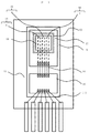
- FIGS. 1 is a schematic plan view of a thermal air flow sensor mounted
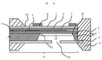
- FIG. 2 is a cross-sectional view taken along the line AA in FIG.
- the thermal air flow sensor of this embodiment has a measuring element 17 and an LSI 16 mounted on a support 9, and is sealed with a resin 11 so that a part of the measuring element 17 is partially exposed. It has been stopped.
- the resin 11 in the vicinity of the partially exposed region is formed in a tapered shape.
- the region other than the partially exposed region, that is, the outside of the resin end portion 13 is originally covered with the resin 11 and cannot be viewed from the outside.
- the portion covered with the resin 11 is also visible.
- the measuring element 17 and the LSI 16 are electrically connected via the wire 10.
- the measuring element 17 has a diaphragm 18 and measures the amount of intake air by the heating resistor 15 provided on the diaphragm 18 and the side temperature resistors 14 provided on the upstream side and the downstream side of the heating resistor, respectively. ing.
- a lead frame, a ceramic substrate, or the like is employed as the support 9, a lead frame, a ceramic substrate, or the like.
- the silicon substrate 1 is thermally oxidized to form a thermal oxide film 2 as a lower electrical insulating film.
- an anti-separation material 3 of 20 to 50 nm, platinum (Pt), molybdenum (Mo), etc.
- the metal film 4 is sequentially deposited to a thickness of about 150 nm and patterned to form the resistance temperature detector 14, the heating resistor 15, and the wiring of these resistors.
- the lower electrical insulating film may be the thermal oxide film 2 alone, but a silicon nitride (SiN) film or a silicon oxide film (SiO 2 ) may be laminated.
- a silicon oxide film 5 serving as an upper electrical insulating film is deposited on the temperature measuring resistor 14 and the heating resistor 15 by a plasma CVD method to a thickness of about 500 nm, and then heat treatment is performed at 800 ° C. or higher for the purpose of densifying the film. I do.
- the resistance temperature detector 14 and the heating resistor 15 have a pattern, when the silicon oxide film 5 is formed after the side temperature resistor 14 and the heating resistor 15 are formed, the silicon oxide film 5 is formed.
- a step occurs. When this step causes some mechanical side effect, the step may be eliminated by mechanical polishing or the like.
- a silicon nitride film 6 is deposited to a thickness of about 200 nm by plasma CVD, and then heat treatment is performed at 800 ° C. or higher for the purpose of densifying the film.
- a silicon oxide film 7 is deposited with a film thickness of 300 to 500 nm by plasma CVD, and then heat treatment is performed at 800 ° C. or higher.
- a polyimide organic film is deposited and patterned on the silicon oxide film 7 to form a PIQ film 8 so as to expose a part of the diaphragm. Since the end portion 12 of the diaphragm 18 is protected by the highly elastic PIQ film 8, the destruction of the diaphragm 18 due to the collision of dust can be suppressed.
- the PIQ film 8 is formed so as to expose a part of the diaphragm 18.
- the measurement element 17 is completed by forming the diaphragm 18 from the back surface using a silicon oxide film or the like as a mask material and using an etching solution such as KOH.
- the diaphragm 18 may be formed using a dry etching method.
- the measuring element 17 is affixed on the support 9 with a die bond tape or the like, and then the support 9 on which the measuring element 17 or the like is mounted is placed in a resin casting mold, and the insert is pushed into an area where it is desired to partially expose.
- the resin 11 is poured into the resin casting mold and sealed with resin, thereby completing the thermal air flow sensor in which the region including the diaphragm 18 is partially exposed.
- the support 9 is provided with a ventilation hole 19 for preventing the space on the back side of the diaphragm 18 from being sealed.
- Figure 3 shows the results of evaluating the peel strength of the interface by a scratch test.
- the vertical axis represents the peel strength ratio based on the peel strength at the Pt film / silicon oxide film interface.
- the case where Cr, Ti, TiN, ALN, MoN, and WN are deposited as a single layer film as the peeling prevention material 3 is shown, but at least two kinds of Cr, Ti, TiN, ALN, MoN, and WN are shown.
- the peel strength of the structure in which these films are laminated is improved as in the case of the single-layer film.
- Ti is disposed under the Pt film or the molybdenum film, a reaction layer is formed at the interface, and the temperature dependence of the resistance change described later is extremely reduced. Therefore, TiN, By depositing ALN, WN or the like, it is possible to suppress a decrease in temperature dependency of the resistance change of the metal film 4.
- the uppermost layer of the laminated film is composed of a film made of any of TiN, ALN, and WN, formation of a reaction layer by the metal film 4 and the Ti film can be reliably prevented.
- the peeling prevention material 3 needs to be provided in a region where peeling occurs, it is necessary to be provided at a place where the insert piece is pressed, that is, at a wiring portion in a region partially exposed from the resin 11. In particular, it may be provided in a region near the resin 11 in the exposed portion.
- FIGS. A second embodiment of the present invention will be described with reference to FIGS. Note that the description of the same parts as in the first embodiment is omitted.
- the second embodiment of the present invention is characterized in that no peeling prevention material 3 under the resistance temperature detector 14 is provided.
- the resistance temperature detectors 14 are arranged on the upstream side and the downstream side of the heating resistor 15, and the resistance change due to the temperature difference between the upstream and downstream resistance temperature detectors is measured. From this, the air flow rate is calculated. Therefore, it is preferable that the temperature dependence of the resistance change is large because the flow rate can be measured with high sensitivity.
- the peeling prevention material 3 is disposed in the lower layer of the resistance temperature detector 14, the temperature dependence of the resistance change of the side temperature resistance 14 is lowered, which is not preferable when it is desired to measure the flow rate with high sensitivity.
- the insert When the region including the diaphragm 18 is partially exposed, the insert is pressed against the silicon substrate surface so that the region including the diaphragm 18 is hidden by the insert, and then the resin is injected.
- the diaphragm 18 is thinner than the other portions, if the insert piece is directly pressed, the diaphragm 18 is deformed, and an error occurs in detection accuracy. Therefore, the insert piece has a recess so that the insert piece is not directly pressed against the diaphragm 18, and the area around the diaphragm 18 is pressed by the pressing portion provided on the outer peripheral edge of the recess. . That is, since the insert piece is not directly pressed against the diaphragm 18, the metal film and the electrical insulating film are not peeled off.
- the anti-separation material 3 is provided in the region pressed against the insert, that is, the lower layer of the wiring portion formed outside the diaphragm 18, and the region not pressed against the insert, ie, the diaphragm 18 is provided.
- the metal film formed in this embodiment, in particular, the peeling prevention material is not provided in the lower layer of the side temperature resistor 14 where the temperature dependence of the resistance change is important.
- the anti-separation material 3 is not provided on the diaphragm 18, but is provided only on the lower layer of the wiring portion provided on the Si substrate. As described above, the region where the tip of the insert piece is pressed is always only on the silicon substrate 1 excluding the diaphragm 18. Like the second embodiment, the third embodiment can prevent separation with high flow accuracy. Further, the heating resistor 15 and the side temperature resistor 14 provided on the same diaphragm 18 are not provided with an anti-separation material and have a similar structure, so that the measurement element 17 can be easily manufactured. There are also advantages.
- the detailed region where the tip of the insert piece is pressed is a region between the resin end 13 and the diaphragm end 12, and therefore, as shown in FIG. It is arranged. Since the separation preventing material 3 is provided in the minimum necessary region, it is possible to prevent the separation at a low cost.
Landscapes
- Physics & Mathematics (AREA)
- Fluid Mechanics (AREA)
- General Physics & Mathematics (AREA)
- Measuring Volume Flow (AREA)
Abstract
本発明の目的は、熱式空気流量センサにおいて、測定素子の配線等のはく離を抑制し、信頼性の高い熱式空気流量センサを提供することにある。上記目的を達成するために、本発明の熱式空気流量センサは、発熱抵抗体と前記発熱抵抗体の上下流にそれぞれ設けられる側温抵抗体を有するダイアフラムと、前記発熱抵抗体および測温抵抗体の配線が配置される配線部と、を有する半導体基板と、前記半導体基板を封止する樹脂と、を備え、前記樹脂は前記ダイアフラムを含む領域を部分的に露出する露出部を有する熱式流量センサにおいて、前記露出部にある配線部の下層に、Cr、Ti、TiN、ALN、MoN、WNのいずれかからなる単層膜を設けることを特徴とする。
Description
本発明は、熱式空気流量センサに係り、特に自動車エンジンの吸気系に設置してエンジンの吸入空気流量を測定する熱式空気流量センサに関する。
エンジンの吸入空気量を測定する空気流量計として、エンジン内に吸入される空気量を直接検知できる熱式の空気流量計が主流になっている。特に、半導体マイクロマシニング技術により製造された測定素子を備えた熱式の空気流量計は、コストが低減できることや、低電力で駆動できることなどから注目されている。このような熱式の空気流量計に用いられる測定素子としては、例えば特許文献1に提案されているものがある。この公報に提案されている測定素子は、半導体基板上に電気絶縁膜が形成され、この電気絶縁膜上に発熱抵抗体や測温抵抗体が形成されており、さらに発熱抵抗体、測温抵抗体の上には電気絶縁体が形成されている。また、発熱抵抗体や測温抵抗体が形成された領域は、半導体基板の裏面側から異方性エッチングすることにより半導体基板の一部が除去されてダイアフラム構造となっている。
また、特許文献2には、半導体チップを樹脂封止する表面実装構型電子部品およびその製造方法において、封止樹脂の経時劣化が発生せず、信頼性が高く、低コストで量産性を向上することを目的として、シリコーンゴム製の封止樹脂防止部材を光電効果素子部の表面に載置して光電効果素子部の表面を覆った状態で封止樹脂を注入し、光電効果素子部の表面を除いて樹脂封止部を形成することが開示されている。
ダイアフラムを有する半導体基板や半導体基板を実装する支持体等を樹脂封止により一体に成形する場合、測定の原理上、発熱抵抗体や測温抵抗体が形成されたダイアフラム領域は樹脂で覆わずに部分的に露出させ、吸入空気に接するようにしなければならない。封止樹脂がダイアフラムを覆わないようにする部分露出構造とするためには、樹脂注形金型とは別に設けられた、駆動可能な金型(入れ駒)で半導体基板のダイアフラム周辺を押さえつけ、樹脂がダイアフラムに流れ込まないようにする必要がある。ここで、ダイアフラムに樹脂が流れ込まないようにするために、ある程度の力で入れ駒を半導体基板に押し付ける必要があるので、半導体基板の部分露出部には外部から応力が印加されることとなる。そのため、入れ駒を押し付けるダイアフラム周辺の配線等のはく離強度が低い場合には、この応力により配線等がはく離してしまう虞がある。ここで、配線部にはく離が発生すると、配線部の抵抗が変化する場合があり、そのような場合には流量検出に誤差が生じてしまう虞がある。特許文献1および特許文献2は、上記課題についてはなんら考慮がされていない。
本発明の目的は、熱式空気流量センサにおいて、測定素子の配線等のはく離を抑制し、信頼性の高い熱式空気流量センサを提供することにある。
上記目的を達成するために、本発明の熱式空気流量センサは、発熱抵抗体と前記発熱抵抗体の上下流にそれぞれ設けられる側温抵抗体を有するダイアフラムと、前記発熱抵抗体および測温抵抗体の配線が配置される配線部と、を有する半導体基板と、 前記半導体基板を封止する樹脂と、を備え、前記樹脂は前記ダイアフラムを含む領域を部分的に露出する露出部を有する熱式流量センサにおいて、前記露出部にある配線部の下層に、Cr、Ti、TiN、ALN、MoN、WNのいずれかからなる単層膜を設けることを特徴とする。
本発明によれば、測定素子の配線等のはく離を抑制し、信頼性の高い熱式空気流量センサを提供することができる。
以下、本発明の実施例を説明する。
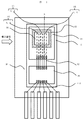
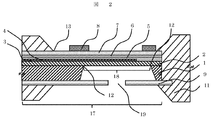
本発明の第一の実施例である熱式空気流量センサを図1と図2を用いて説明する。図1は熱式空気流量センサの実装概略平面図、図2は図1のA-A位置における断面図である。
本実施例の熱式空気流量センサは、図1に示すように、測定素子17とLSI16を支持体9上に搭載し、測定素子17の一部を部分的に露出するように樹脂11により封止されている。部分的に露出している領域近傍の樹脂11はテーパ状に形成されている。ここで、部分的に露出されている領域以外、すなわち樹脂端部13より外側は、本来は樹脂11に覆われているので外部から見ることはできないが、図1においては、樹脂11を透過させて樹脂11に覆われている部分も見えるような記載としている。測定素子17とLSI16はワイヤ10を介して電気的に接続されている。測定素子17は、ダイアフラム18を有していて、ダイアフラム18上に設けられる発熱抵抗体15と、発熱抵抗体の上流側と下流側にそれぞれ設けられる側温抵抗体14により吸入空気量を測定している。なお、支持体9としては、リードフレームやセラミック基板などが採用される。
図2を用いて本実施例の製造方法を説明する。
まずは、測定素子17の製造方法について詳述する。シリコン基板1を熱酸化して下部電気絶縁膜となる熱酸化膜2を形成し、熱酸化膜2の上に、はく離防止材3を20~50nm、プラチナ(Pt)やモリブデン(Mo)などの金属膜4を150nm厚ほど順次堆積してパターニングを行うことにより、測温抵抗体14や発熱抵抗体15及びこれら抵抗体の配線を形成する。なお、下部電気絶縁膜は熱酸化膜2だけでも良いが、シリコンナイトライド(SiN)膜やシリコン酸化膜(SiO2)を積層しても良い。次に測温抵抗体14と発熱抵抗体15の上に上部電気絶縁膜となる、シリコン酸化膜5を500nm程度プラズマCVD法により堆積し、その後、膜の緻密化を目的に800℃以上で熱処理を行う。ここで、測温抵抗体14や発熱抵抗体15はパターンを有しているので、側温抵抗体14や発熱抵抗体15を形成してからシリコン酸化膜5を形成すると、シリコン酸化膜5に段差が発生する。この段差が何らかの機械的副作用を生じさせる場合には、機械研磨等により段差を解消してもよい。次に、プラズマCVD法によりシリコンナイトライド膜6を200nm程度堆積し、その後、膜の緻密化を目的に800℃以上で熱処理を行う。その後、シリコン酸化膜7を300~500nmの膜厚でプラズマCVD法により堆積し、その後、800℃以上で熱処理を行う。次にポリイミド系の有機膜をシリコン酸化膜7上に堆積・パターニングを行い、ダイアフラムの一部を露出するようにPIQ膜8を形成する。弾性の高いPIQ膜8でダイアフラム18の端部12を保護する構成となっているので、ダストの衝突によるダイアフラム18の破壊を抑制することができる。また、吸入空気量を測定する発熱抵抗体15および側温抵抗体14を直接吸入空気にさらす必要があるので、ダイアフラム18の一部を露出させるようにPIQ膜8を形成している。次に、裏面よりシリコン酸化膜等をマスク材として、KOHなどのエッチング液を用いてダイアフラム18を形成することで測定素子17が完成する。なお、ダイアフラム18は、ドライエッチング法を用いて形成しても良い。
次に測定素子17を支持体9上にダイボンドテープ等で貼り付け、その後、測定素子17などを搭載した支持体9を樹脂注型金型に配置し、入れ駒を部分露出させたい領域に押し当てて樹脂注型金型に樹脂11を流し込み、樹脂封止することで、ダイアフラム18を含む領域を部分露出させた熱式空気流量センサが完成する。また、支持体9には、ダイアフラム18の裏面側の空間部を密封させないための換気孔19が設けられている。
次に、本実施例の作用効果について説明する。
金属膜4とシリコン酸化膜等の電気絶縁膜との界面のはく離強度は、一般に低いことが知られている。このため、ダイアフラム領域を樹脂により部分露出する際に、入れ駒の先端部を測定素子17に押し当てる際の荷重が大きい場合には、入れ駒を押し当てている領域、すなわち部分的に樹脂11から露出している領域にある金属膜4と電気絶縁膜との界面ではく離が発生する可能性がある。そこで、金属膜4と電気絶縁膜のはく離強度向上を目的に、入れ駒が押し当たる箇所を含む領域の金属膜4となるPt膜と電気絶縁膜となるシリコン酸化膜界面に、Cr,Ti,TiN、ALN、MoN、WNのいずれかからなる膜(はく離防止材3)を堆積させる。
スクラッチ試験により、その界面のはく離強度を評価した結果を図3に示す。縦軸はPt膜/シリコン酸化膜界面のはく離強度を基準にした場合のはく離強度比を示す。Cr,Ti,TiN、ALN、MoN、WNのいずれかからなる単層膜では、何れの場合でも、Cr,Ti,TiN、ALN、MoN、WN膜を介在させない場合よりもはく離強度が向上した。はく離強度は、WN=MoN=ALN<TiN<Ti<Crの順で高くなることが分かった。金属膜4として、MoなどのPt以外の金属膜でも同様の実験を行ったところ、はく離強度の依存性はほぼ同様(図示せず)であり、はく離強度を向上させるために金属膜4と電気絶縁膜の間にCr,Ti,TiN、ALN、MoN、WNのいずれかからなる膜を設けることが有効であると判明した。これは、金属膜4およびシリコン酸化膜等の電気絶縁膜の両方と密着性の高い膜を、金属膜4と電気絶縁膜の間に介在させることで、膜同士の密着性を向上させているからである。
第一実施例では、はく離防止材3としてCr,Ti,TiN、ALN、MoN、WNを単層膜として堆積した場合を示したが、Cr,Ti,TiN、ALN、MoN、WNの少なくとも2種類の膜を積層した構造についても、単層膜同様にはく離強度が向上することは言うまでもない。特にPt膜やモリブデン膜の下にTiを配置させた場合では界面に反応層が形成され、後述する抵抗変化の温度依存性が極端に低下するので、Ti膜と金属膜4の間にTiN、ALN、WN等を堆積することで金属膜4の抵抗変化の温度依存性の低下を抑制することができる。特に、積層膜の最上層をTiN、ALN、WNのいずれかからなる膜で構成すると、金属膜4とTi膜による反応層の形成を確実に防止できる。
はく離防止材3は、はく離が発生する領域に設ける必要があるので、入れ駒が押し当てられる箇所、すなわち部分的に樹脂11から露出されている領域の配線部に設けられている必要がある。特に露出部の樹脂11近傍の領域に設けられていると良い。
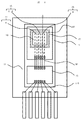
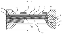
本発明の第二実施例を図4および図5を用いて説明する。なお、第一実施例と構成が同じ部分は説明を省略する。
図4に示すように、本発明の第二の実施例では、測温抵抗体14の下のはく離防止材3を設けていないことを特徴とする。MEMS式の流量測定は、発熱抵抗体15の上流側と下流側に測温抵抗体14を配置し、上流と下流の測温抵抗体個所での温度差による抵抗変化を計測し、この抵抗変化から空気流量を算出する。そのため、抵抗変化の温度依存性が大きい方が高感度に流量測定が可能となるので好ましい。しかし、はく離防止材3を測温抵抗体14の下層に配置すると、側温抵抗体14の抵抗変化の温度依存性が低下してしまうので、高感度に流量を測定したい場合には好ましくない。そのため、温度変化によって抵抗が変化し、この出力を何らかの制御に使うような個所へのはく離防止材3適用は、あまり適していないので、ダイアフラム18上に設けられている測温抵抗体14へのはく離防止材3の適用を回避させている。
ダイアフラム18を含む領域を部分的に露出する構造とするときに、入れ駒をシリコン基板表面に押し当てて、ダイアフラム18を含む領域を入れ駒で隠すようにしてから樹脂を注入している。ここで、ダイアフラム18は他の部分よりも薄い構成であるので、入れ駒を直接押し当ててしまうとダイアフラム18に変形が生じてしまい、検出精度に誤差が生じるようになる。そのため、ダイアフラム18に入れ駒が直接押し当てられないように、入れ駒は凹部を有していて、この凹部外周縁に設けられた押し当て部でダイアフラム18周辺の領域を押し当てるようにしている。すなわち、ダイアフラム18には入れ駒が直接押し当てられないので、金属膜と電気絶縁膜とのはく離が発生しない。
第二実施例によると、入れ駒に押し当てられる領域、すなわちダイアフラム18の外側に形成される配線部の下層にはく離防止材3を設けていて、入れ駒に押し当てられない領域、すなわちダイアフラム18に形成される金属膜、特に抵抗変化の温度依存性が重要である側温抵抗体14の下層にははく離防止材を設けない構成としている。上記構成により、流量検出精度を維持しつつ、金属膜4のはく離を防止することができる。第二実施例によると高い流量精度ではく離を防止することができる。
第二実施例の変形例を、図7を用いて説明する。
図7に示すように、はく離防止材3をダイアフラム18上に設けずに、Si基板上に設けられた配線部の下層のみに設けた構成としたものである。上述したとおり、入れ駒の先端部が押しつけられる領域は、ダイアフラム18を除く、シリコン基板1上のみと必ずなる。第二実施例同様に、第三実施例においても高い流量精度ではく離を防止することができる。さらに、同一ダイアフラム18上に設けられている発熱抵抗体15と側温抵抗体14にはく離防止材を設けておらず、似たような構成とするので、測定素子17の製造が簡単になるという利点もある。
さらなる変形例としては、入れ駒の先端部が押しつけられる詳しい領域は、樹脂端部13とダイアフラム端部12の間の領域であるので、図6に示すように、この領域のみにはく離防止材3を配置させている。必要最小限の領域にはく離防止材3を設ける構成としているので、低コストではく離を防止することが可能となる。
1 シリコン基板
2 熱酸化膜
3 はく離防止材
4 金属膜
5 シリコン酸化膜
6 シリコンナイトライド膜
7 シリコン酸化膜
8 PIQ膜
9 支持体
10 ワイヤ
11 樹脂
12 ダイアフラム端部
13 樹脂端部
14 測温抵抗体
15 発熱抵抗体
16 LSI
17 測定素子
18 ダイアフラム
19 換気孔
2 熱酸化膜
3 はく離防止材
4 金属膜
5 シリコン酸化膜
6 シリコンナイトライド膜
7 シリコン酸化膜
8 PIQ膜
9 支持体
10 ワイヤ
11 樹脂
12 ダイアフラム端部
13 樹脂端部
14 測温抵抗体
15 発熱抵抗体
16 LSI
17 測定素子
18 ダイアフラム
19 換気孔
Claims (9)
- 発熱抵抗体と前記発熱抵抗体の上下流にそれぞれ設けられる側温抵抗体を有するダイアフラムと、前記発熱抵抗体および測温抵抗体の配線が配置される配線部と、を有する半導体基板と、
前記半導体基板を封止する樹脂と、を備え、
前記樹脂は前記ダイアフラムを含む領域を部分的に露出する露出部を有する熱式流量センサにおいて、
前記露出部にある配線部の下層に、Cr、Ti、TiN、ALN、MoN、WNのいずれかからなる単層膜を設けることを特徴とする熱式空気流量センサ。 - 請求項1に記載の熱式空気流量センサにおいて、
前記単層膜は、前記側温抵抗体の下層には設けられず、前記露出部にある配線部の下層に設けられることを特徴とする熱式空気流量センサ。 - 請求項1に記載の熱式空気流量センサにおいて、
前記単層膜は、前記発熱抵抗体の下層には設けられず、前記露出部にある配線部の下層に設けられることを特徴とする熱式空気流量センサ。 - 請求項1に記載の熱式空気流量センサにおいて、
前記単層膜は、前記ダイアフラムには設けられず、前記配線部の下層のみ設けられることを特徴とする熱式空気流量センサ。 - 発熱抵抗体と前記発熱抵抗体の上下流にそれぞれ設けられる側温抵抗体を有するダイアフラムと、前記発熱抵抗体および測温抵抗体の配線が配置される配線部と、を有する半導体基板と、
前記半導体基板を封止する樹脂と、を備え、
前記樹脂は前記ダイアフラムを含む領域を部分的に露出する露出部を有する熱式流量センサにおいて、
前記露出部にある配線部の下層に、Cr、Ti、TiN、ALN、MoN、WNのうち少なくとも2種類からなる積層膜を設けることを特徴とする熱式空気流量センサ。 - 請求項5に記載の熱式流量センサにおいて、
前記積層膜の最上層は、TiN、ALN、WNのいずれかからなることを特徴とする熱式流量センサ。 - 請求項5に記載の熱式空気流量センサにおいて、
前記積層膜は、前記側温抵抗体の下層には設けられず、前記露出部にある配線部の下層に設けられることを特徴とする熱式空気流量センサ。 - 請求項5に記載の熱式空気流量センサにおいて、
前記積層膜は、前記発熱抵抗体の下層には設けられず、前記露出部にある配線部の下層に設けられることを特徴とする熱式空気流量センサ。 - 請求項5に記載の熱式空気流量センサにおいて、
前記積層膜は、前記ダイアフラムには前記積層膜を設けられず、前記配線部の下層のみに設けられていることを特徴とする熱式空気流量センサ。
Applications Claiming Priority (2)
| Application Number | Priority Date | Filing Date | Title |
|---|---|---|---|
| JP2012146287A JP5768011B2 (ja) | 2012-06-29 | 2012-06-29 | 熱式空気流量センサ |
| JP2012-146287 | 2012-06-29 |
Publications (1)
| Publication Number | Publication Date |
|---|---|
| WO2014002737A1 true WO2014002737A1 (ja) | 2014-01-03 |
Family
ID=49782902
Family Applications (1)
| Application Number | Title | Priority Date | Filing Date |
|---|---|---|---|
| PCT/JP2013/065913 Ceased WO2014002737A1 (ja) | 2012-06-29 | 2013-06-10 | 熱式空気流量センサ |
Country Status (2)
| Country | Link |
|---|---|
| JP (1) | JP5768011B2 (ja) |
| WO (1) | WO2014002737A1 (ja) |
Cited By (4)
| Publication number | Priority date | Publication date | Assignee | Title |
|---|---|---|---|---|
| CN106932039A (zh) * | 2015-12-15 | 2017-07-07 | 株式会社堀场制作所 | 流量测量装置、燃料消耗量测量装置和流量测量方法 |
| WO2017174565A1 (en) | 2016-04-07 | 2017-10-12 | Arcelik Anonim Sirketi | A dishwasher |
| WO2020094296A1 (en) | 2018-11-06 | 2020-05-14 | Arcelik Anonim Sirketi | A dishwasher comprising a drawer |
| WO2020136260A1 (en) | 2018-12-28 | 2020-07-02 | Arcelik Anonim Sirketi | A dishwasher |
Families Citing this family (1)
| Publication number | Priority date | Publication date | Assignee | Title |
|---|---|---|---|---|
| JP2020169929A (ja) * | 2019-04-04 | 2020-10-15 | 株式会社デンソー | 物理量計測装置 |
Citations (1)
| Publication number | Priority date | Publication date | Assignee | Title |
|---|---|---|---|---|
| JP2007294870A (ja) * | 2006-03-30 | 2007-11-08 | Mitsui Mining & Smelting Co Ltd | 薄膜センサ、薄膜センサモジュールおよび薄膜センサの製造方法 |
-
2012
- 2012-06-29 JP JP2012146287A patent/JP5768011B2/ja not_active Expired - Fee Related
-
2013
- 2013-06-10 WO PCT/JP2013/065913 patent/WO2014002737A1/ja not_active Ceased
Patent Citations (1)
| Publication number | Priority date | Publication date | Assignee | Title |
|---|---|---|---|---|
| JP2007294870A (ja) * | 2006-03-30 | 2007-11-08 | Mitsui Mining & Smelting Co Ltd | 薄膜センサ、薄膜センサモジュールおよび薄膜センサの製造方法 |
Cited By (4)
| Publication number | Priority date | Publication date | Assignee | Title |
|---|---|---|---|---|
| CN106932039A (zh) * | 2015-12-15 | 2017-07-07 | 株式会社堀场制作所 | 流量测量装置、燃料消耗量测量装置和流量测量方法 |
| WO2017174565A1 (en) | 2016-04-07 | 2017-10-12 | Arcelik Anonim Sirketi | A dishwasher |
| WO2020094296A1 (en) | 2018-11-06 | 2020-05-14 | Arcelik Anonim Sirketi | A dishwasher comprising a drawer |
| WO2020136260A1 (en) | 2018-12-28 | 2020-07-02 | Arcelik Anonim Sirketi | A dishwasher |
Also Published As
| Publication number | Publication date |
|---|---|
| JP5768011B2 (ja) | 2015-08-26 |
| JP2014010025A (ja) | 2014-01-20 |
Similar Documents
| Publication | Publication Date | Title |
|---|---|---|
| US9851233B2 (en) | Physical quantity sensor | |
| CN106840291B (zh) | 热式空气流量传感器 | |
| JP5012330B2 (ja) | センサ装置の製造方法及びセンサ装置 | |
| JP5768011B2 (ja) | 熱式空気流量センサ | |
| US20180202958A1 (en) | Gas sensor with a gas permeable region | |
| US8104355B2 (en) | Thermal humidity sensor | |
| JP4952428B2 (ja) | センサ装置 | |
| US7404321B2 (en) | Sensor device having a buffer element between the molding and the sensing element | |
| JP2009270930A (ja) | 熱式流量センサ | |
| JP5093052B2 (ja) | 熱式流量センサ | |
| US11435310B2 (en) | Humidity sensor | |
| JP5857050B2 (ja) | 流量計 | |
| JP5243348B2 (ja) | 流量検出装置 | |
| JP5841918B2 (ja) | センサ装置 | |
| CN112880903A (zh) | 压阻式压力芯片及制备方法 | |
| JP2003021547A (ja) | 薄膜式センサならびにフローセンサおよびその製造方法 | |
| JP5949573B2 (ja) | 物理量センサの製造方法 | |
| JP5092936B2 (ja) | 熱式流量センサ及びその製造方法 | |
| JP5768179B2 (ja) | 熱式空気流量センサ | |
| WO2015182257A1 (ja) | 流量センサおよびその製造方法 | |
| JPWO2003102974A1 (ja) | 白金薄膜および熱式センサ | |
| TWI247102B (en) | Semiconductor pressure sensor and method of making the same | |
| JP2021061378A (ja) | 半導体チップの製造方法 |
Legal Events
| Date | Code | Title | Description |
|---|---|---|---|
| 121 | Ep: the epo has been informed by wipo that ep was designated in this application |
Ref document number: 13809717 Country of ref document: EP Kind code of ref document: A1 |
|
| NENP | Non-entry into the national phase |
Ref country code: DE |
|
| 122 | Ep: pct application non-entry in european phase |
Ref document number: 13809717 Country of ref document: EP Kind code of ref document: A1 |