WO2013190893A1 - 電子部品の実装方法 - Google Patents
電子部品の実装方法 Download PDFInfo
- Publication number
- WO2013190893A1 WO2013190893A1 PCT/JP2013/061426 JP2013061426W WO2013190893A1 WO 2013190893 A1 WO2013190893 A1 WO 2013190893A1 JP 2013061426 W JP2013061426 W JP 2013061426W WO 2013190893 A1 WO2013190893 A1 WO 2013190893A1
- Authority
- WO
- WIPO (PCT)
- Prior art keywords
- electronic component
- main body
- electrode
- substrate
- double layer
- Prior art date
- Legal status (The legal status is an assumption and is not a legal conclusion. Google has not performed a legal analysis and makes no representation as to the accuracy of the status listed.)
- Ceased
Links
Images


Classifications
-
- H—ELECTRICITY
- H01—ELECTRIC ELEMENTS
- H01G—CAPACITORS; CAPACITORS, RECTIFIERS, DETECTORS, SWITCHING DEVICES, LIGHT-SENSITIVE OR TEMPERATURE-SENSITIVE DEVICES OF THE ELECTROLYTIC TYPE
- H01G2/00—Details of capacitors not covered by a single one of groups H01G4/00-H01G11/00
- H01G2/02—Mountings
- H01G2/04—Mountings specially adapted for mounting on a chassis
-
- H—ELECTRICITY
- H01—ELECTRIC ELEMENTS
- H01G—CAPACITORS; CAPACITORS, RECTIFIERS, DETECTORS, SWITCHING DEVICES, LIGHT-SENSITIVE OR TEMPERATURE-SENSITIVE DEVICES OF THE ELECTROLYTIC TYPE
- H01G11/00—Hybrid capacitors, i.e. capacitors having different positive and negative electrodes; Electric double-layer [EDL] capacitors; Processes for the manufacture thereof or of parts thereof
- H01G11/78—Cases; Housings; Encapsulations; Mountings
-
- Y—GENERAL TAGGING OF NEW TECHNOLOGICAL DEVELOPMENTS; GENERAL TAGGING OF CROSS-SECTIONAL TECHNOLOGIES SPANNING OVER SEVERAL SECTIONS OF THE IPC; TECHNICAL SUBJECTS COVERED BY FORMER USPC CROSS-REFERENCE ART COLLECTIONS [XRACs] AND DIGESTS
- Y02—TECHNOLOGIES OR APPLICATIONS FOR MITIGATION OR ADAPTATION AGAINST CLIMATE CHANGE
- Y02E—REDUCTION OF GREENHOUSE GAS [GHG] EMISSIONS, RELATED TO ENERGY GENERATION, TRANSMISSION OR DISTRIBUTION
- Y02E60/00—Enabling technologies; Technologies with a potential or indirect contribution to GHG emissions mitigation
- Y02E60/13—Energy storage using capacitors
Definitions
- the present invention relates to an electronic component mounting method, and more particularly, to an electronic component mounting method for mounting an electronic component such as an electric double layer capacitor having a main body and an extraction electrode drawn out of the main body on a substrate.
- Patent Document 1 An example of a conventional electrochemical device such as an electric double layer capacitor which is the background of the present invention is disclosed in Japanese Patent Application Laid-Open No. 2002-151021 (see Patent Document 1).
- the electrochemical device disclosed in Patent Document 1 includes an exterior body and an electrochemical element body enclosed in the exterior body, and an extraction electrode of the electrochemical element body protrudes outside the exterior body. ing.
- the electrochemical device disclosed in Patent Document 1 described above occupies at least a portion corresponding to a substantially rectangular portion surrounding the exterior body and the extraction electrode of the electrochemical device. Will do.
- electronic components have been mounted at high density, and it is required to further reduce the area occupied by the electronic components.
- a main object of the present invention is to provide an electronic component mounting method capable of reducing the mounting area of the electronic component.
- An electronic component mounting method is an electronic component mounting method for mounting an electronic component having a main body and an extraction electrode drawn out of the main body on a substrate, the electronic component extraction electrode
- the electronic component mounting method is characterized in that after the substrate is bonded to the substrate, the extraction electrode is folded back to the mounting surface side of the main body facing the substrate when the electronic component is mounted on the substrate, starting from a part of the extraction electrode. is there.
- the main body has a convex portion on the mounting surface side, and the lead-out electrode and the substrate are pulled out so that at least a part of the joint portion is located at a portion other than the convex portion of the main body. It is preferable that the portion is folded.
- the main body includes, for example, an electronic component element that is weak against heat and has an electrolyte or an organic conductor.
- the extraction electrode of the electronic component is joined to the substrate, the extraction electrode is folded back to the mounting surface side of the main body starting from a part of the extraction electrode. A part of the electronic component is opposed to the main body of the electronic component on the substrate, so that the mounting area of the electronic component can be reduced.
- the extraction electrodes are mounted on the mounting surface of the main body starting from a part of the extraction electrode. By folding back to the side, even if there are a plurality of extraction electrodes, the mounting area of the electronic component can be reduced.
- the main body has a convex part on the mounting surface side, and the lead-out electrode and the substrate are drawn out so that at least a part of the joint part is located in a part other than the convex part of the main body.
- the part is folded back, at least a part of the joint between the extraction electrode and the substrate is housed in a part other than the convex part, so that the mounting area of the electronic part can be reduced and the increase in the mounting height of the electronic part can be suppressed. it can.
- the extraction electrode is folded after the extraction electrode is bonded to the substrate, heat generated when the extraction electrode of the electronic component is bonded is prevented from being applied to the main body of the electronic component. be able to. Therefore, in the electronic component mounting method according to the present invention, when the main body includes an electrolyte or an organic conductor that is weak against heat, for example, when the electronic component mounting method according to the present invention is applied to the storage device mounting method, The following effects occur. It is possible to prevent the electrolyte solution in the electronic component body from being dried up or the resistance of the organic conductor from increasing. Moreover, damage to the sealing part of the main body of the electronic component can be prevented, which leads to prevention of short circuit failure and moisture intrusion into the main body.
- the mounting area of the electronic component can be reduced.
- FIG. 1 It is a perspective view which shows an example of the electrical double layer capacitor as an electronic component to which this invention is applied. It is a cross-sectional solution figure which shows the internal structure of the electric double layer capacitor shown in FIG. It is a perspective view which shows the state which mounted the electric double layer capacitor shown in FIG. 1 on the board
- FIG. 1 is a perspective view showing an example of an electric double layer capacitor as an electronic component to which the present invention is applied
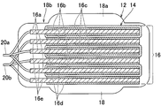
- FIG. 2 is a sectional schematic view showing an internal structure of the electric double layer capacitor shown in FIG.
- FIG. 3 is a perspective view showing a state where the electric double layer capacitor shown in FIG. 1 is mounted on a substrate.
- the main body 12 includes an electronic component element 14 as shown in FIG.
- the electronic component element 14 includes a positive electrode current collector 16a made of, for example, Al foil, a positive electrode active material 16b made of, for example, activated carbon, a separator 16c, a negative electrode active material 16d, made of, for example, activated carbon, and a negative electrode current collector 16e made of, for example, Al foil.
- the laminated body 16 is impregnated with an electrolytic solution.
- the main body 12 further includes a film outer package 18, and the film outer package 18 seals the electronic component element 14.
- the film outer package 18 has a convex portion 18 a at the approximate center on the mounting surface side of the main body 12, and has a portion 18 b other than the convex portion adjacent to the convex portion 18 a on one side of the mounting surface side of the main body 12.
- the mounting surface side of the main body 12 is a surface side facing the substrate of the main body 12 when the electric double layer capacitor 10 is mounted on the substrate.
- the electric double layer capacitor 10 further includes, for example, a strip-like positive electrode lead electrode 20a and a negative electrode lead electrode 20b.
- the positive electrode lead electrode 20a is electrically connected to the positive electrode current collector 16a of the electronic component element 14, and the negative electrode lead electrode 20b. Is electrically connected to the negative electrode current collector 16 e of the electronic component element 14. Further, the positive electrode lead electrode 20 a and the negative electrode lead electrode 20 b are drawn to the outside of the main body 12 from the same side of the main body 12 on the side having the portion 18 b other than the convex portion of the film outer package 18.
- the width of the main body 12 is formed to 20 mm
- the length of the main body 12 is formed to 17 mm
- the length of each of the positive electrode lead electrode 20a and the negative electrode lead electrode 20b is 3 mm.
- the thickness of the main body 12 is 3 mm.
- the tip portion 22a of the positive electrode lead electrode 20a and the tip portion 22b of the negative electrode lead electrode 20b are connected to each electrode (not shown) of the substrate (not shown) using solders 30a and 30b. Are joined by soldering to each other (not shown).
- the convex portion 18a and the portion 18b other than the convex portion of the film outer package 18 of the main body 12 do not face the substrate and face the opposite side of the substrate.
- the tip portion 22a of the positive electrode lead electrode 20a, the tip portion 22b of the negative electrode lead electrode 20b, and the substrate The positive electrode lead electrode 20a and the negative electrode lead electrode 20b are connected to the main body 12 so that the joint portions 32a and 32b with the respective solder electrodes 30a and 30b are located on the portion 18b other than the convex portion of the film outer package 18 of the main body 12. Fold it back to the mounting surface.
- the electric double layer capacitor 10 is mounted on the substrate.
- the mounting area of the electric double layer capacitor 10 mounted on the substrate was measured.
- the width of the mounted portion (the width of the main body 12) is 20 mm
- the height of the electric double layer capacitor 10 mounted on the substrate was measured. As a result, in the example, the height was 3 mm, and in the comparative example, the height was 3 mm.
- the mounting area of the electric double layer capacitor 10 was reduced as compared with the comparative example. This is because, in the mounting method of the embodiment, after the tip portion 22a of the positive electrode lead electrode 20a and the tip portion 22b of the negative electrode lead electrode 20b of the electric double layer capacitor 10 are joined to each electrode of the substrate, the end of the positive electrode lead electrode 20a Since the positive electrode lead electrode 20a and the negative electrode lead electrode 20b are folded back to the mounting surface side of the main body 12 starting from the portion 24a and the end portion 24b of the negative electrode lead electrode 20b, the tip portion 22a of the positive electrode lead electrode 20a of the electric double layer capacitor 10 and This is because the tip portion 22b of the negative electrode lead electrode 20b faces the portion of the main body 12 of the electric double layer capacitor 10 on the substrate, so that the mounting area of the electric double layer capacitor 10 can be reduced.
- the positive electrode lead electrode 20a and the negative electrode lead electrode 20b are provided, and the positive electrode lead electrode 20a and the negative electrode lead electrode 20b are drawn from the same side of the main body 12. Even if the positive electrode lead electrode 20a and the negative electrode lead electrode 20b are provided by folding the positive electrode lead electrode 20a and the negative electrode lead electrode 20b to the mounting surface side of the main body 12 starting from the portion 24a and the end portion 24b of the negative electrode lead electrode 20b, The mounting area of the electric double layer capacitor 10 can be reduced.
- the main body 12 has the convex portion 18a on the film outer package 18 on the mounting surface side, and the tip portion 22a of the positive electrode lead electrode 20a and the tip portion 22b of the negative electrode lead electrode 20b Since the positive electrode lead-out electrode 20a and the negative electrode lead-out electrode 20b are folded back so that the joint portions 32a and 32b with the respective electrodes are located on the portion 18b other than the convex portion of the film outer package 18 of the main body 12, the tip portion 22a of the positive electrode lead-out electrode 20a Since the joint portions 32a and 32b between the tip portion 22b of the negative electrode lead-out electrode 20b and each electrode of the substrate are accommodated in the portion 18b other than the convex portion, the mounting area of the electric double layer capacitor 10 can be reduced, and the electric double layer An increase in the mounting height of the capacitor 10 can be suppressed.
- the positive electrode lead electrode 20a and the negative electrode lead electrode 20b are folded after the tip portion 22a of the positive electrode lead electrode 20a and the tip portion 22b of the negative electrode lead electrode 20b are joined to each electrode of the substrate. Heat generated when the positive electrode lead electrode 20 a and the negative electrode lead electrode 20 b of the electric double layer capacitor 10 are joined can be prevented from being applied to the main body 12 of the electric double layer capacitor 10.
- Drying up of the electrolyte in the main body 12 of the electric double layer capacitor 10 can be prevented. Moreover, damage to the sealing part of the main body 12 of the electric double layer capacitor 10 can be prevented, leading to prevention of short circuit failure and moisture intrusion into the main body 12. Furthermore, damage to the separator 16c in the main body 12 of the electric double layer capacitor 10 can be reduced, leading to prevention of short circuit failure.
- the main body 12 is formed in a substantially rectangular plate shape, but the main body may be formed in other shapes such as a polygonal plate shape and a disk shape in addition to the substantially rectangular plate shape. .
- the extraction electrode 20a (20b) is formed in a strip shape, but the extraction electrode may be formed in other shapes such as a rod shape or a line shape in addition to the strip shape.
- the positive electrode lead electrode 20a and the negative electrode lead electrode 20b are folded back starting from the end portion 24a of the positive electrode lead electrode 20a and the end portion 24b of the negative electrode lead electrode 20b. What is necessary is just to set suitably according to the mounting area.
- the positive electrode lead electrode 20a and the negative electrode lead electrode 20b start from the intermediate portion between the tip portion 22a and the end portion 24a of the positive electrode lead electrode 20a and the intermediate portion between the tip portion 22b and the end portion 24b of the negative electrode lead electrode 20b. It may be folded back to the 12 mounting surface side.
- the main body 12 includes the film outer package 18 whose both side portions are bent inward, but the main body 12 may be formed in other structures.
- the method for mounting the electric double layer capacitor having the structure including the electrolytic solution has been described as an example.
- the present invention is also applied to the method for mounting the electric double layer capacitor having the structure including the organic conductor. Can be done. In this case, there is also an effect that it is possible to prevent the resistance of the organic conductor in the electric double layer capacitor from increasing.
- the method for mounting the electric double layer capacitor having two lead electrodes has been described as an example.
- the present invention is not limited to the method for mounting an electronic component having three or more lead electrodes or the electric double layer.
- the present invention can also be applied to a method for mounting electronic components other than capacitors.
- the electronic component mounting method according to the present invention is particularly suitable for a method of mounting an electronic component such as an electric double layer capacitor on a substrate.
Landscapes
- Engineering & Computer Science (AREA)
- Power Engineering (AREA)
- Microelectronics & Electronic Packaging (AREA)
- Electric Double-Layer Capacitors Or The Like (AREA)
Description
この発明は、電子部品の実装方法に関し、特に本体と本体の外側に引き出されている引き出し電極とを有するたとえば電気二重層キャパシタなどの電子部品を基板に実装するための電子部品の実装方法に関する。
この発明の背景となる従来の電気二重層キャパシタなどの電気化学デバイスの一例が、特開2002-151021公報に開示されている(特許文献1参照)。特許文献1に開示されている電気化学デバイスは、外装体と、この外装体の中に封入された電気化学素体とを有し、電気化学素体の引き出し電極が外装体の外部に突き出されている。
上述の特許文献1に開示されている電気化学デバイスを基板に実装した場合、電気化学デバイスは、少なくとも電気化学デバイスの外装体および引き出し電極を囲む略矩形状の部分に対応する部分だけ基板を占有することになる。
昨今、電子部品の高密度実装化が進み、電子部品が基板を占有する面積をさらに低減することが求められている。
昨今、電子部品の高密度実装化が進み、電子部品が基板を占有する面積をさらに低減することが求められている。
それゆえに、この発明の主たる目的は、電子部品の実装面積を低減できる、電子部品の実装方法を提供することである。
この発明にかかる電子部品の実装方法は、本体とその本体の外側に引き出されている引き出し電極とを有する電子部品を基板に実装するための電子部品の実装方法であって、電子部品の引き出し電極を基板に接合した後に、引き出し電極の一部分を起点として引き出し電極を、電子部品を基板に実装したときに基板に対向する本体の実装面側に折り返すことを特徴とする、電子部品の実装方法である。
この発明にかかる電子部品の実装方法では、引き出し電極を2つ以上有し、全ての引き出し電極が本体の同一辺から引き出されていることが好ましい。
また、この発明にかかる電子部品の実装方法では、本体は実装面側に凸部を有し、引き出し電極と基板との接合部の少なくとも一部分が本体の凸部以外の部分に位置するように引き出し部を折り返すことを特徴とすることが好ましい。
さらに、この発明にかかる電子部品の実装方法では、本体は、たとえば、電解液または有機導電体を有する熱に弱い電子部品素子を含むことを特徴とする。
この発明にかかる電子部品の実装方法では、引き出し電極を2つ以上有し、全ての引き出し電極が本体の同一辺から引き出されていることが好ましい。
また、この発明にかかる電子部品の実装方法では、本体は実装面側に凸部を有し、引き出し電極と基板との接合部の少なくとも一部分が本体の凸部以外の部分に位置するように引き出し部を折り返すことを特徴とすることが好ましい。
さらに、この発明にかかる電子部品の実装方法では、本体は、たとえば、電解液または有機導電体を有する熱に弱い電子部品素子を含むことを特徴とする。
この発明にかかる電子部品の実装方法では、電子部品の引き出し電極が基板に接合された後に、引き出し電極の一部分を起点として引き出し電極が本体の実装面側に折り返されるので、電子部品の引き出し電極の一部が電子部品の本体部分に基板上で対向し、そのため、電子部品の実装面積を低減できる。
この発明にかかる電子部品の実装方法において、引き出し電極を2つ以上有し、全ての引き出し電極が本体の同一辺から引き出されていると、引き出し電極の一部分を起点として引き出し電極が本体の実装面側に折り返されることによって、引き出し電極が複数あっても、電子部品の実装面積を低減できる。
また、この発明にかかる電子部品の実装方法において、本体は実装面側に凸部を有し、引き出し電極と基板との接合部の少なくとも一部分が本体の凸部以外の部分に位置するように引き出し部を折り返すと、引き出し電極と基板との接合部の少なくとも一部分が凸部以外の部分に収納されるため、電子部品の実装面積を低減できるとともに、電子部品の実装高さの増加を抑えることができる。
さらに、この発明にかかる電子部品の実装方法によれば、引き出し電極を基板に接合した後に引き出し電極を折り返すので、電子部品の引き出し電極の接合時に生じる熱が電子部品の本体に加わることを防止することができる。
そのため、この発明にかかる電子部品の実装方法において、本体が熱に弱い電解液または有機導電体を含む場合、たとえば、この発明にかかる電子部品の実装方法を蓄電デバイスの実装方法に適用した場合、次の効果が生じる。
電子部品の本体内の電解液のドライアップまたは有機導電体の抵抗が高くなることを防止できる。
また、電子部品の本体の封止部へのダメージを防止でき、ショート不良や本体の内部への水分の浸入の防止につながる。
この発明にかかる電子部品の実装方法において、引き出し電極を2つ以上有し、全ての引き出し電極が本体の同一辺から引き出されていると、引き出し電極の一部分を起点として引き出し電極が本体の実装面側に折り返されることによって、引き出し電極が複数あっても、電子部品の実装面積を低減できる。
また、この発明にかかる電子部品の実装方法において、本体は実装面側に凸部を有し、引き出し電極と基板との接合部の少なくとも一部分が本体の凸部以外の部分に位置するように引き出し部を折り返すと、引き出し電極と基板との接合部の少なくとも一部分が凸部以外の部分に収納されるため、電子部品の実装面積を低減できるとともに、電子部品の実装高さの増加を抑えることができる。
さらに、この発明にかかる電子部品の実装方法によれば、引き出し電極を基板に接合した後に引き出し電極を折り返すので、電子部品の引き出し電極の接合時に生じる熱が電子部品の本体に加わることを防止することができる。
そのため、この発明にかかる電子部品の実装方法において、本体が熱に弱い電解液または有機導電体を含む場合、たとえば、この発明にかかる電子部品の実装方法を蓄電デバイスの実装方法に適用した場合、次の効果が生じる。
電子部品の本体内の電解液のドライアップまたは有機導電体の抵抗が高くなることを防止できる。
また、電子部品の本体の封止部へのダメージを防止でき、ショート不良や本体の内部への水分の浸入の防止につながる。
この発明によれば、電子部品の実装面積を低減できる。
この発明の上述の目的、その他の目的、特徴および利点は、図面を参照して行う以下の発明を実施するための形態の説明から一層明らかとなろう。
(実施例)
図1は、この発明が適用される電子部品としての電気二重層キャパシタの一例を示す斜視図であり、図2は、図1に示す電気二重層キャパシタの内部構造を示す断面図解図であり、図3は、図1に示す電気二重層キャパシタを基板に実装した状態を示す斜視図である。
図1は、この発明が適用される電子部品としての電気二重層キャパシタの一例を示す斜視図であり、図2は、図1に示す電気二重層キャパシタの内部構造を示す断面図解図であり、図3は、図1に示す電気二重層キャパシタを基板に実装した状態を示す斜視図である。
図1に示す電気二重層キャパシタ10は、たとえば略矩形板状の本体12を含む。
本体12は、図2に示すように、電子部品素子14を含む。電子部品素子14は、たとえばAl箔からなる正極集電体16a、たとえば活性炭からなる正極活物質16b、セパレータ16c、たとえば活性炭からなる負極活物質16d、および、たとえばAl箔からなる負極集電体16eを有する積層体16を含み、積層体16には電解液が含浸されている。
本体12は、さらにフィルム外装体18を含み、フィルム外装体18は、電子部品素子14を封止する。フィルム外装体18は、本体12の実装面側の略中央に凸部18aを有し、本体12の実装面側の一辺側に凸部18aに隣接して凸部以外の部分18bを有する。ここで、本体12の実装面側とは、電気二重層キャパシタ10を基板に実装したときに、本体12の基板に対向する面側である。
電気二重層キャパシタ10は、たとえば帯状の正極引き出し電極20aおよび負極引き出し電極20bをさらに含み、正極引き出し電極20aは、電子部品素子14の正極集電体16aに電気的に接続され、負極引き出し電極20bは、電子部品素子14の負極集電体16eに電気的に接続される。また、正極引き出し電極20aおよび負極引き出し電極20bは、本体12のフィルム外装体18の凸部以外の部分18bを有する側の同一辺から本体12の外側に引き出されている。
図1に示す電気二重層キャパシタ10は、たとえば、本体12の幅が20mmに形成され、本体12の長さが17mmに形成され、正極引き出し電極20aおよび負極引き出し電極20bのそれぞれの長さが3mmに形成され、本体12の厚さが3mmに形成されている。
そして、図1に示す電気二重層キャパシタ10において、正極引き出し電極20aの先端部分22aおよび負極引き出し電極20bの先端部分22bを、はんだ30aおよび30bを用いて基板(図示せず)の各電極(図示せず)にそれぞれはんだ付けすることによって接合する。この場合、本体12のフィルム外装体18の凸部18aおよび凸部以外の部分18bは、基板には対向せず、基板とは反対側を向いている。
その後に、図3に示すように、正極引き出し電極20aの末端部分24aおよび負極引き出し電極20bの末端部分24bを起点として、正極引き出し電極20aの先端部分22aおよび負極引き出し電極20bの先端部分22bと基板の各電極とのはんだ30aおよび30bによる接合部32aおよび32bが、本体12のフィルム外装体18の凸部以外の部分18bに位置するように、正極引き出し電極20aおよび負極引き出し電極20bを本体12の実装面側に折り返す。
このようにして、電気二重層キャパシタ10を基板に実装する。
(比較例)
比較例では、実施例と同様に、図1に示す電気二重層キャパシタ10において、正極引き出し電極20aの先端部分22aおよび負極引き出し電極20bの先端部分22bを、はんだ30aおよび30bを用いて基板の各電極にそれぞれはんだ付けすることによって接合する。ただし、その後、正極引き出し電極20aおよび負極引き出し電極20bは、折り返さない。このようにして、電気二重層キャパシタ10を基板に実装する。
比較例では、実施例と同様に、図1に示す電気二重層キャパシタ10において、正極引き出し電極20aの先端部分22aおよび負極引き出し電極20bの先端部分22bを、はんだ30aおよび30bを用いて基板の各電極にそれぞれはんだ付けすることによって接合する。ただし、その後、正極引き出し電極20aおよび負極引き出し電極20bは、折り返さない。このようにして、電気二重層キャパシタ10を基板に実装する。
ここで、上述の実施例および比較例において、基板に実装した電気二重層キャパシタ10の実装面積を測定した。
実施例では、実装した部分の幅(本体12の幅)が20mmであり、実装した部分の長さ(本体12と正極引き出し電極20aおよび負極引き出し電極20bとを平面的に見た長さ)が17mmであった。そのため、実施例では、電気二重層キャパシタ10の実装面積は、20mm×17mm=340mm2であった。
一方、比較例では、実装した部分の幅(本体12の幅)が20mmであり、実装した部分の長さ(本体12と正極引き出し電極20aおよび負極引き出し電極20bとを平面的に見た長さ)が20mmであった。そのため、比較例では、電気二重層キャパシタ10の実装面積は、20mm×20mm=400mm2であった。
実施例では、実装した部分の幅(本体12の幅)が20mmであり、実装した部分の長さ(本体12と正極引き出し電極20aおよび負極引き出し電極20bとを平面的に見た長さ)が17mmであった。そのため、実施例では、電気二重層キャパシタ10の実装面積は、20mm×17mm=340mm2であった。
一方、比較例では、実装した部分の幅(本体12の幅)が20mmであり、実装した部分の長さ(本体12と正極引き出し電極20aおよび負極引き出し電極20bとを平面的に見た長さ)が20mmであった。そのため、比較例では、電気二重層キャパシタ10の実装面積は、20mm×20mm=400mm2であった。
さらに、実施例および比較例において、基板に実装した電気二重層キャパシタ10の高さを測定した。
その結果、実施例では、その高さが3mmであり、比較例でもその高さが3mmであった。
その結果、実施例では、その高さが3mmであり、比較例でもその高さが3mmであった。
上述のように、実施例では、比較例と比べて、電気二重層キャパシタ10の実装面積が低減していることがわかった。
これは、実施例の実装方法では、電気二重層キャパシタ10の正極引き出し電極20aの先端部分22aおよび負極引き出し電極20bの先端部分22bが基板の各電極に接合された後に、正極引き出し電極20aの末端部分24aおよび負極引き出し電極20bの末端部分24bを起点として正極引き出し電極20aおよび負極引き出し電極20bが本体12の実装面側に折り返されるので、電気二重層キャパシタ10の正極引き出し電極20aの先端部分22aおよび負極引き出し電極20bの先端部分22bが電気二重層キャパシタ10の本体12の部分に基板上で対向し、そのため、電気二重層キャパシタ10の実装面積を低減できるからである。
これは、実施例の実装方法では、電気二重層キャパシタ10の正極引き出し電極20aの先端部分22aおよび負極引き出し電極20bの先端部分22bが基板の各電極に接合された後に、正極引き出し電極20aの末端部分24aおよび負極引き出し電極20bの末端部分24bを起点として正極引き出し電極20aおよび負極引き出し電極20bが本体12の実装面側に折り返されるので、電気二重層キャパシタ10の正極引き出し電極20aの先端部分22aおよび負極引き出し電極20bの先端部分22bが電気二重層キャパシタ10の本体12の部分に基板上で対向し、そのため、電気二重層キャパシタ10の実装面積を低減できるからである。
上述の実施例の実装方法において、正極引き出し電極20aおよび負極引き出し電極20bを有し、正極引き出し電極20aおよび負極引き出し電極20bが本体12の同一辺から引き出されているので、正極引き出し電極20aの末端部分24aおよび負極引き出し電極20bの末端部分24bを起点として正極引き出し電極20aおよび負極引き出し電極20bが本体12の実装面側に折り返されることによって、正極引き出し電極20aおよび負極引き出し電極20bがあっても、電気二重層キャパシタ10の実装面積を低減できる。
また、上述の実施例の実装方法において、本体12は実装面側においてフィルム外装体18に凸部18aを有し、正極引き出し電極20aの先端部分22aおよび負極引き出し電極20bの先端部分22bと基板の各電極との接合部32aおよび32bが本体12のフィルム外装体18の凸部以外の部分18bに位置するように正極引き出し電極20aおよび負極引き出し電極20bを折り返すので、正極引き出し電極20aの先端部分22aおよび負極引き出し電極20bの先端部分22bと基板の各電極との接合部32aおよび32bが凸部以外の部分18bに収納されるため、電気二重層キャパシタ10の実装面積を低減できるとともに、電気二重層キャパシタ10の実装高さの増加を抑えることができる。
さらに、実施例の実装方法によれば、正極引き出し電極20aの先端部分22aおよび負極引き出し電極20bの先端部分22bを基板の各電極に接合した後に正極引き出し電極20aおよび負極引き出し電極20bを折り返すので、電気二重層キャパシタ10の正極引き出し電極20aおよび負極引き出し電極20bの接合時に生じる熱が電気二重層キャパシタ10の本体12に加わることを防止することができる。
そのため、次の効果が生じる。
電気二重層キャパシタ10の本体12内の電解液のドライアップを防止できる。
また、電気二重層キャパシタ10の本体12の封止部へのダメージを防止でき、ショート不良や本体12の内部への水分の浸入の防止につながる。
さらに、電気二重層キャパシタ10の本体12内のセパレータ16cへのダメージを低減でき、ショート不良の防止につながる。
電気二重層キャパシタ10の本体12内の電解液のドライアップを防止できる。
また、電気二重層キャパシタ10の本体12の封止部へのダメージを防止でき、ショート不良や本体12の内部への水分の浸入の防止につながる。
さらに、電気二重層キャパシタ10の本体12内のセパレータ16cへのダメージを低減でき、ショート不良の防止につながる。
なお、上述の実施例では、本体12が略矩形板状に形成されているが、本体は、略矩形板状以外にたとえば多角形板状や円板状など他の形状に形成されてもよい。
また、上述に実施例では、引き出し電極20a(20b)が帯状に形成されているが、引き出し電極は、帯状以外にたとえば棒状や線状など他の形状に形成されてもよい。
さらに、上述の実施例では、正極引き出し電極20aの末端部分24aおよび負極引き出し電極20bの末端部分24bを起点として正極引き出し電極20aおよび負極引き出し電極20bが折り返されているが、折り返しの起点は、所望の実装面積に応じて適宜設定すればよい。たとえば、正極引き出し電極20aの先端部分22aおよび末端部分24a間の中間部分と負極引き出し電極20bの先端部分22bおよび末端部分24b間の中間部分とを起点として正極引き出し電極20aおよび負極引き出し電極20bが本体12の実装面側に折り返されてもよい。
さらに、上述の実施例では、本体12が、両側部分が内側に折り曲げられているフィルム外装体18を含むが、本体12は、他の構造に形成されてもよい。
また、上述の実施例では、電解液を含む構造の電気二重層キャパシタの実装方法を例にして説明したが、この発明は、有機導電体を含む構造の電気二重層キャパシタの実装方法にも適用されうる。この場合、電気二重層キャパシタ内の有機導電体の抵抗が高くなることを防止できるという効果も奏する。
さらに、上述の実施例では、2つの引き出し電極を有する電気二重層キャパシタの実装方法を例にして説明したが、この発明は、3つ以上の引き出し電極を有する電子部品の実装方法や電気二重層キャパシタ以外の電子部品の実装方法にも適用されうる。
この発明にかかる電子部品の実装方法は、特に、たとえば電気二重層キャパシタなどの電子部品を基板に実装する方法に好適に用いられる。
10 電気二重層キャパシタ
12 本体
14 電子部品素子
16 積層体
16a 正極集電体
16b 正極活物質
16c セパレータ
16d 負極活物質
16e 負極集電体
18 フィルム外装体
18a 凸部
18b 凸部以外の部分
20a 正極引き出し電極
20b 負極引き出し電極
22a、22b 先端部分
24a、24b 末端部分
30a、30b はんだ
32a、32b 接合部
12 本体
14 電子部品素子
16 積層体
16a 正極集電体
16b 正極活物質
16c セパレータ
16d 負極活物質
16e 負極集電体
18 フィルム外装体
18a 凸部
18b 凸部以外の部分
20a 正極引き出し電極
20b 負極引き出し電極
22a、22b 先端部分
24a、24b 末端部分
30a、30b はんだ
32a、32b 接合部
Claims (4)
- 本体と前記本体の外側に引き出されている引き出し電極とを有する電子部品を基板に実装するための電子部品の実装方法であって、
前記電子部品の前記引き出し電極を前記基板に接合した後に、前記引き出し電極の一部分を起点として前記引き出し電極を、前記電子部品を前記基板に実装したときに前記基板に対向する前記本体の実装面側に折り返すことを特徴とする、電子部品の実装方法。 - 前記引き出し電極を2つ以上有し、全ての引き出し電極が前記本体の同一辺から引き出されている、請求項1に記載の電子部品の実装方法。
- 前記本体は実装面側に凸部を有し、前記引き出し電極と前記基板との接合部の少なくとも一部分が前記本体の凸部以外の部分に位置するように前記引き出し部を折り返すことを特徴とする、請求項1または請求項2に記載の電子部品の実装方法。
- 前記本体は、熱に弱い電子部品素子を含むことを特徴とする、請求項1ないし請求項3のいずれかに記載の電子部品の実装方法。
Applications Claiming Priority (2)
| Application Number | Priority Date | Filing Date | Title |
|---|---|---|---|
| JP2012-140983 | 2012-06-22 | ||
| JP2012140983 | 2012-06-22 |
Publications (1)
| Publication Number | Publication Date |
|---|---|
| WO2013190893A1 true WO2013190893A1 (ja) | 2013-12-27 |
Family
ID=49768500
Family Applications (1)
| Application Number | Title | Priority Date | Filing Date |
|---|---|---|---|
| PCT/JP2013/061426 Ceased WO2013190893A1 (ja) | 2012-06-22 | 2013-04-17 | 電子部品の実装方法 |
Country Status (1)
| Country | Link |
|---|---|
| WO (1) | WO2013190893A1 (ja) |
Cited By (1)
| Publication number | Priority date | Publication date | Assignee | Title |
|---|---|---|---|---|
| US11830672B2 (en) | 2016-11-23 | 2023-11-28 | KYOCERA AVX Components Corporation | Ultracapacitor for use in a solder reflow process |
Citations (7)
| Publication number | Priority date | Publication date | Assignee | Title |
|---|---|---|---|---|
| JPS5431554A (en) * | 1977-08-12 | 1979-03-08 | Michio Tsujiura | Stopper for capacitor resistor to be inserted into printed board |
| JP2004266091A (ja) * | 2003-02-28 | 2004-09-24 | Kanebo Ltd | フィルム型蓄電装置 |
| JP2009032612A (ja) * | 2007-07-30 | 2009-02-12 | Sanyo Electric Co Ltd | ラミネート外装電池 |
| JP2010245486A (ja) * | 2009-04-03 | 2010-10-28 | Far East Engineering Co Ltd | 縦型チップコンデンサ |
| JP2011096899A (ja) * | 2009-10-30 | 2011-05-12 | Tdk Corp | ラジアルリード電子部品 |
| JP2011216859A (ja) * | 2010-03-15 | 2011-10-27 | Seiko Instruments Inc | 端子付電気化学セルとその製造方法 |
| JP2012099645A (ja) * | 2010-11-02 | 2012-05-24 | Mitsubishi Electric Corp | 蓄電装置 |
-
2013
- 2013-04-17 WO PCT/JP2013/061426 patent/WO2013190893A1/ja not_active Ceased
Patent Citations (7)
| Publication number | Priority date | Publication date | Assignee | Title |
|---|---|---|---|---|
| JPS5431554A (en) * | 1977-08-12 | 1979-03-08 | Michio Tsujiura | Stopper for capacitor resistor to be inserted into printed board |
| JP2004266091A (ja) * | 2003-02-28 | 2004-09-24 | Kanebo Ltd | フィルム型蓄電装置 |
| JP2009032612A (ja) * | 2007-07-30 | 2009-02-12 | Sanyo Electric Co Ltd | ラミネート外装電池 |
| JP2010245486A (ja) * | 2009-04-03 | 2010-10-28 | Far East Engineering Co Ltd | 縦型チップコンデンサ |
| JP2011096899A (ja) * | 2009-10-30 | 2011-05-12 | Tdk Corp | ラジアルリード電子部品 |
| JP2011216859A (ja) * | 2010-03-15 | 2011-10-27 | Seiko Instruments Inc | 端子付電気化学セルとその製造方法 |
| JP2012099645A (ja) * | 2010-11-02 | 2012-05-24 | Mitsubishi Electric Corp | 蓄電装置 |
Cited By (1)
| Publication number | Priority date | Publication date | Assignee | Title |
|---|---|---|---|---|
| US11830672B2 (en) | 2016-11-23 | 2023-11-28 | KYOCERA AVX Components Corporation | Ultracapacitor for use in a solder reflow process |
Similar Documents
| Publication | Publication Date | Title |
|---|---|---|
| JP5320404B2 (ja) | 電気化学デバイス | |
| JP5588338B2 (ja) | 電気化学デバイス | |
| JP5879491B2 (ja) | 固体電解コンデンサ | |
| US10734161B2 (en) | Multilayer electronic component and board having the same | |
| JP4930124B2 (ja) | 固体電解コンデンサ | |
| JP2009194061A (ja) | 固体電解コンデンサ | |
| JP6232587B2 (ja) | 固体電解コンデンサ | |
| WO2013190893A1 (ja) | 電子部品の実装方法 | |
| JP2009200378A (ja) | 複合型金属化フィルムコンデンサ | |
| JP2009188195A (ja) | 電気化学デバイス及びその実装構造 | |
| JP4985571B2 (ja) | 電子部品およびその製造方法 | |
| KR101337373B1 (ko) | 표면 실장형 슈퍼 커패시터 | |
| US8755171B2 (en) | Stacked-type solid electrolytic capacitor package structure | |
| JP5180657B2 (ja) | 電気化学デバイス | |
| JP5276207B2 (ja) | 電気化学デバイス | |
| CN204117860U (zh) | 具有改进的内部熔丝结构的电力电容器 | |
| JP4654929B2 (ja) | チップ形固体電解コンデンサ | |
| JP2008235412A (ja) | 固体電解コンデンサ | |
| JP2010021317A (ja) | 電子部品およびその製造方法 | |
| JP2019062068A (ja) | 蓄電モジュール | |
| JP4953043B2 (ja) | 電解コンデンサ | |
| KR101139758B1 (ko) | 전해콘덴서의 소자 구조 | |
| JP2012182291A (ja) | 固体電解コンデンサ | |
| KR200338985Y1 (ko) | 전해 콘덴서의 리드선 테이핑구조 | |
| JP2015029008A (ja) | チップ型電子部品 |
Legal Events
| Date | Code | Title | Description |
|---|---|---|---|
| 121 | Ep: the epo has been informed by wipo that ep was designated in this application |
Ref document number: 13806953 Country of ref document: EP Kind code of ref document: A1 |
|
| NENP | Non-entry into the national phase |
Ref country code: DE |
|
| 122 | Ep: pct application non-entry in european phase |
Ref document number: 13806953 Country of ref document: EP Kind code of ref document: A1 |
|
| NENP | Non-entry into the national phase |
Ref country code: JP |