WO2013190664A1 - フレキシブルケーブル、フレキシブルケーブルの接続機構、配線基板および電子機器 - Google Patents
フレキシブルケーブル、フレキシブルケーブルの接続機構、配線基板および電子機器 Download PDFInfo
- Publication number
- WO2013190664A1 WO2013190664A1 PCT/JP2012/065764 JP2012065764W WO2013190664A1 WO 2013190664 A1 WO2013190664 A1 WO 2013190664A1 JP 2012065764 W JP2012065764 W JP 2012065764W WO 2013190664 A1 WO2013190664 A1 WO 2013190664A1
- Authority
- WO
- WIPO (PCT)
- Prior art keywords
- connector
- flexible cable
- terminal portion
- frame
- opening
- Prior art date
- Legal status (The legal status is an assumption and is not a legal conclusion. Google has not performed a legal analysis and makes no representation as to the accuracy of the status listed.)
- Ceased
Links
Images




Classifications
-
- H—ELECTRICITY
- H01—ELECTRIC ELEMENTS
- H01R—ELECTRICALLY-CONDUCTIVE CONNECTIONS; STRUCTURAL ASSOCIATIONS OF A PLURALITY OF MUTUALLY-INSULATED ELECTRICAL CONNECTING ELEMENTS; COUPLING DEVICES; CURRENT COLLECTORS
- H01R12/00—Structural associations of a plurality of mutually-insulated electrical connecting elements, specially adapted for printed circuits, e.g. printed circuit boards [PCB], flat or ribbon cables, or like generally planar structures, e.g. terminal strips, terminal blocks; Coupling devices specially adapted for printed circuits, flat or ribbon cables, or like generally planar structures; Terminals specially adapted for contact with, or insertion into, printed circuits, flat or ribbon cables, or like generally planar structures
- H01R12/70—Coupling devices
- H01R12/77—Coupling devices for flexible printed circuits, flat or ribbon cables or like structures
- H01R12/79—Coupling devices for flexible printed circuits, flat or ribbon cables or like structures connecting to rigid printed circuits or like structures
-
- H—ELECTRICITY
- H01—ELECTRIC ELEMENTS
- H01R—ELECTRICALLY-CONDUCTIVE CONNECTIONS; STRUCTURAL ASSOCIATIONS OF A PLURALITY OF MUTUALLY-INSULATED ELECTRICAL CONNECTING ELEMENTS; COUPLING DEVICES; CURRENT COLLECTORS
- H01R12/00—Structural associations of a plurality of mutually-insulated electrical connecting elements, specially adapted for printed circuits, e.g. printed circuit boards [PCB], flat or ribbon cables, or like generally planar structures, e.g. terminal strips, terminal blocks; Coupling devices specially adapted for printed circuits, flat or ribbon cables, or like generally planar structures; Terminals specially adapted for contact with, or insertion into, printed circuits, flat or ribbon cables, or like generally planar structures
- H01R12/70—Coupling devices
- H01R12/82—Coupling devices connected with low or zero insertion force
- H01R12/85—Coupling devices connected with low or zero insertion force contact pressure producing means, contacts activated after insertion of printed circuits or like structures
- H01R12/88—Coupling devices connected with low or zero insertion force contact pressure producing means, contacts activated after insertion of printed circuits or like structures acting manually by rotating or pivoting connector housing parts
Definitions
- the disclosed embodiment relates to a flexible cable, a flexible cable connection mechanism, a wiring board, and an electronic device.
- FPC Flexible Printed Circuit
- the FPC cable has a terminal portion at its end, which is connected to a connector mounted on a printed circuit board (hereinafter referred to as “PCB”) of an electronic device. Connected.
- PCB printed circuit board
- an FPC cable that includes a frame-like protruding portion formed using FPC at the terminal portion and can be connected while surrounding the outer periphery of the connector at the inner periphery of the protruding portion (for example, , See Patent Document 1).
- the conventional FPC cable and its connection mechanism have room for further improvement in terms of suppressing noise without hindering downsizing of electronic equipment.
- a noise shield body in general, application of a noise shield body can be considered as an effective noise countermeasure in the connection between the PCB and the FPC cable.
- the mechanism in order to effectively suppress noise, the mechanism tends to be large or complicated in order to reliably ground the noise shield body to the ground. For this reason, there existed a possibility of inhibiting size reduction of an electronic device.
- One aspect of the embodiment is made in view of the above, and includes a flexible cable, a flexible cable connection mechanism, a wiring board, and an electronic device that can suppress noise without hindering downsizing of the electronic device.
- the purpose is to provide.
- the flexible cable which concerns on 1 aspect of embodiment is provided with a terminal part, a frame, a pattern wiring, and an opening part.
- the terminal portion is connected to a connector provided on the wiring board.
- the frame is provided on the terminal portion.
- the pattern wiring is formed on the frame and is covered with insulation. The opening exposes a part of the pattern wiring of the frame.
- noise can be suppressed without hindering downsizing of the electronic device.
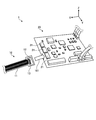
- FIG. 1 is a schematic perspective view illustrating an overall configuration of a flexible cable connection mechanism according to an embodiment.
- FIG. 2 is a schematic top view showing a detailed configuration in the vicinity of the frame.
- FIG. 3 is a schematic perspective view showing the configuration of the connector.
- FIG. 4A is a schematic top view illustrating a connection state between the flexible cable and the connector.
- FIG. 4B is a schematic side view illustrating a connection state between the flexible cable and the connector.
- FIG. 5A is a schematic top view illustrating a connection state between a flexible cable and a connector according to a modification.
- FIG. 5B is a schematic side view illustrating a connection state between the flexible cable and the connector according to the modification.
- FIG. 5A is a schematic top view illustrating a connection state between a flexible cable and a connector according to a modification.
- FIG. 5B is a schematic side view illustrating a connection state between the flexible cable and the connector according to the modification.
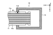
- FIG. 6A is a diagram (part 1) illustrating a processing example for preventing erroneous connection of the flexible cable.
- FIG. 6B is a diagram (part 2) illustrating a processing example for preventing erroneous connection of the flexible cable.
- FIG. 6C is a diagram (part 3) illustrating a processing example for preventing erroneous connection of the flexible cable.
- the flexible cable is an FPC cable and the wiring board is a PCB.
- the connector to which the flexible cable is connected is a ZIF (Zero Insertion Force socket) connector.
- the wiring board is simply referred to as “board”.
- FIG. 1 is a schematic perspective view showing the overall configuration of the connection mechanism 1 of the flexible cable 10 according to the embodiment.
- FIG. 1 shows a three-dimensional orthogonal coordinate system including the Z axis with the vertical upward direction as the positive direction for easy understanding. Such an orthogonal coordinate system may be shown in other drawings used in the following description. In the present embodiment, it is defined that the flexible cable 10 is inserted from the positive direction of the X axis.
- connection mechanism 1 includes a flexible cable 10 and a substrate 20.
- the flexible cable 10 includes a cable part 11, a terminal part 12, and a frame body 13.
- the cable part 11 is a wiring member that covers a pattern wiring made of a conductive foil such as copper by sandwiching an insulating resin film made of polyimide resin or the like from above and below.
- the terminal portion 12 is a terminal portion of the cable portion 11 and is connected to a connector 21 described later.
- the frame body 13 is formed in a shape that can surround the outer periphery of the connector 21 with the inner periphery of the frame body 13 when the terminal portion 12 is connected to the connector 21 (see arrow 101 in the figure).
- FIG. 1 shows a case where the frame 13 has a shape having a substantially rectangular inner periphery when viewed from above, but the shape of the frame 13 is not limited and the connector 21 is not limited. Any shape may be used according to the outer periphery.
- the shape of the frame 13 may be formed so that the terminal portion 12 is correctly connected to the connector 21.
- a low-profile connector 21 is mounted on the board 20. Details of the connector 21 will be described later with reference to FIG. FIG. 1 shows an example in which three connectors 21 having the same orientation are mounted on the board 20, but the orientation, arrangement position, and number of the connectors 21 are not limited. .
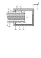
- FIG. 2 is a schematic top view showing a detailed configuration in the vicinity of the frame body 13.
- the cable part 11 has a plurality of pattern wirings 11a arranged substantially in parallel.
- the pattern wiring 11a is formed of a conductor such as copper as described above, and is configured in a multilayer including a signal layer, a ground layer, and the like.
- the pattern wiring 11a is covered with an insulating resin film (hereinafter referred to as “insulating film 11b”) made of a polyimide resin or the like as described above.
- insulating film 11b an insulating resin film made of a polyimide resin or the like as described above.
- the signal layer, the ground layer, and the like described above are laminated in a wafer shape with the insulating film 11b interposed therebetween.
- the cable part 11 has a notch 11c in the vicinity of the end part. Details of the notch 11c will be described later with reference to FIG. 4A.
- terminal part 12 will be provided in the edge part of the cable part 11.
- FIG. The frame body 13 is provided on the terminal portion 12.
- the frame 13 has a noise shield pattern wiring (hereinafter referred to as “shield pattern 13a” for convenience of explanation) of the same layer and the same material as the pattern wiring 11a of the cable portion 11.
- shield pattern 13a a noise shield pattern wiring
- the shield pattern 13 a is formed along the frame of the frame 13 in a substantially U shape excluding the region overlapping the cable portion 11. Note that whether or not the shield pattern 13a is electrically connected to the pattern wiring 11a of the cable portion 11 in the broken line C in the drawing may be appropriately selected depending on the purpose and application.
- the frame 13 has an insulating film 13b.
- the shield pattern 13a is covered with the insulating film 13b in the same manner as the pattern wiring 11a described above.
- the frame 13 has the insulating film 13b opened in a part of the surface facing the substrate 20, and a part of the shield pattern 13a is exposed. Details of this point will be described later with reference to FIG. 4B.
- the shield pattern 13a and the insulating film 13b that form the frame of the frame body 13, and the pattern wiring 11a and the insulating film 11b that form the cable portion 11 have the same layer and the same material.
- the frame body 13 can be manufactured without adding a new process to the manufacturing process of the cable portion 11, for example, by die molding by punching or the like with respect to the outer shape.
- FIG. 3 is a schematic perspective view showing the configuration of the connector 21.
- the connector 21 includes an insertion portion 21a, a lever 21b, and a lock tab 21c.
- the insertion portion 21a is a contact portion into which the terminal portion 12 (see FIG. 2) of the flexible cable 10 is inserted (see an arrow 301 in FIG. 3).
- the lock tab 21c sinks in the direction indicated by the arrow 303 in the figure in conjunction with the lever 21b being tilted in the direction of the arrow 302 in the figure. Then, the lock tab 21c that has sunk engages with the notch 11c of the cable portion 11 described above at the tip thereof, thereby fixing the terminal portion 12 and the connector 21 together. This point will be illustrated in the following description of FIG. 4A.
- FIG. 4A is a schematic top view illustrating a connection state between the flexible cable 10 and the connector 21.
- the connector 21 is surrounded by the frame 13 so that a more reliable removal preventing effect can be obtained.
- the frame 13 surrounds the outer periphery of the connector 21 at its inner periphery.
- the inner periphery of the frame 13 and the outer periphery of the connector 21 are preferably in contact with each other, but may be opposed to each other with a predetermined gap.
- the frame 13 can be hooked on the side surface of the connector 21 against the pulling force applied to the flexible cable 10 from the horizontal direction, so that it is possible to obtain a sure prevention effect against the pulling force applied from the horizontal direction.
- the frame body 13 is preferably provided so as to overlap with the lever 21 b when the lever 21 b is tilted toward the substrate 20.
- the lever 21b can be functioned as a pressing mechanism for the frame body 13, it is possible to obtain a reliable prevention effect against the removal force applied vertically upward.
- solder bumps 22 are provided on the substrate 20 at portions that overlap the frame 13 when the flexible cable 10 and the connector 21 are connected.
- the noise shield body is formed by bringing the solder bumps 22 into contact with a part of the shield pattern 13a of the frame body 13.
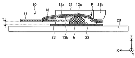
- FIG. 4B is a schematic side view showing a connection state between the flexible cable 10 and the connector 21.
- the solder bump 22 is a ground member having a predetermined height h and being provided in conduction with the ground 23 of the substrate 20.
- the insulating film 13b on the side facing the substrate 20 of the frame 13 is partially opened to form an opening 13c as shown in FIG. 4B.
- the opening 13 c is provided at a portion that overlaps the solder bump 22 when the terminal portion 12 is connected to the connector 21.
- the predetermined height h of the solder bump 22 is “with respect to the height t of the pattern wiring 11a (that is, the shield pattern 13a) from the substrate 20 when the flexible cable 10 and the connector 21 are connected. h> t ”.
- L ′ in the following equation (2) may be substituted for L in the above equation (1).
- the connector 21 surrounded by the noise shield body can enhance its noise resistance.
- solder bumps 22 provided as the ground member can be formed without providing an additional process in the component mounting process on the substrate 20. Moreover, it is not necessary to use special or large parts to form the noise shield body. Therefore, noise can be easily suppressed without hindering downsizing of the electronic device, and cost reduction can be achieved.
- solder bump 22 was used as a ground member so far, it is not restricted to this, For example, it is good also as using a chip component.
- this modification will be described with reference to FIGS. 5A and 5B.
- FIG. 5A is a schematic top view showing a connection state between the flexible cable 10 and the connector 21 according to a modification
- FIG. 5B is a schematic side view showing the connection state.
- FIG. 5A corresponds to FIG. 4A and FIG. 5B corresponds to FIG. 4B, description of constituent elements that overlap with those in the case of using FIGS. 4A and 4B will be omitted as appropriate.
- the substrate 20 may be provided with a chip component 22 ′ such as a square chip fixed resistor or a multilayer ceramic chip capacitor as a ground member instead of the solder bump 22.
- a chip component 22 ′ such as a square chip fixed resistor or a multilayer ceramic chip capacitor as a ground member instead of the solder bump 22.
- the chip component 22 ' is shown in a rectangular parallelepiped shape, but the shape of the chip component 22' is not limited.
- the predetermined height h ′ of the chip component 22 ′ is the height t of the shield pattern 13a from the substrate 20 when the flexible cable 10 and the connector 21 are connected.
- “h ′> t” is preferable.
- solder bump 22 or the chip component 22 ′ is used as the ground member
- the case where one piece is provided at each symmetrical position with respect to the insertion direction of the flexible cable 10 has been described. It does not limit the number.
- the arrangement position may be a portion on the substrate 20 that overlaps at least the frame body 13 when the flexible cable 10 is connected to the connector 21. Further, the number may be one or plural.
- the opening 13c is formed in the frame 13 of the flexible cable 10 and a part of the shield pattern 13a is exposed. There is an effect that can be shown.
- Such an indication of the front and back can contribute to prevention of erroneous connection, but the flexible cable 10 may be further processed to further prevent erroneous connection.
- FIGS. 6A to 6C An example of processing in such a case is shown in FIGS. 6A to 6C.
- 6A to 6C are diagrams illustrating an example in the case where the flexible cable 10 is processed to prevent erroneous connection.
- a seal 11d may be provided on the insulating film 11b of the cable part 11 or the like.
- the mark 11d can be provided by using a technique such as silk screen printing.
- the black mark isosceles triangle represents the mark 11d, but the shape of the mark 11d is not limited.
- the portion to be provided is not limited to the insulating film 11b of the cable portion 11, and may be on the insulating film 13b of the frame 13, for example.
- the front side of the flexible cable 10 is provided on the side where the mark 11d is provided, and the flexible cable 10 is inserted in the apex direction of the isosceles triangle of the mark 11d.
- Each direction can be specified.
- the width of the frame 13 may be different on the left and right. That is, the connector 21 shown so far has a substantially rectangular shape having two sides substantially parallel to the insertion direction of the terminal portion 12 when viewed from above, but the frame body 13 facing each of the two sides has a substantially rectangular shape.
- the widths “W1” and “W2” may be set to “W1 ⁇ W2”, for example.
- the frame body 13 may be provided with a predetermined inclination ⁇ with respect to the extending direction of the cable portion 11 (that is, the X-axis direction). In this case, by predefining the side on which the frame body 13 is inclined as the front side, it is possible to contribute to prevention of erroneous connection.
- the flexible cable according to the embodiment includes a terminal portion, a frame, a pattern wiring, and an opening.
- the terminal portion is connected to a connector provided on the wiring board.
- the frame is provided on the terminal portion.
- the pattern wiring is formed on the frame and insulated.
- the opening exposes a part of the pattern wiring of the frame.
- the flexible cable is an FPC cable
- the flexible cable is not limited to this as long as it has flexibility, for example, FFC (Flexible Flat Cable) or the like. There may be.
- the connector is a ZIF connector
- the present invention is not limited to this.
- the present invention may be applied to a connector that does not have a terminal portion locking mechanism such as a ZIF connector.
- the frame body surrounds the outer periphery of the connector, so that at least the removal force from the horizontal direction can be surely prevented from being pulled out, and noise suppression can be achieved as in the case of the ZIF connector. be able to.
Landscapes
- Details Of Connecting Devices For Male And Female Coupling (AREA)
- Coupling Device And Connection With Printed Circuit (AREA)
Description
開示の実施形態は、フレキシブルケーブル、フレキシブルケーブルの接続機構、配線基板および電子機器に関する。
従来、携帯電話やノート型パソコンといった電子機器の小型化や高性能化が図られるにつれ、これら電子機器に用いられる配線部材もまた、さらなる取り回しの良さや省スペースでの高密度化が図られてきた。
たとえば、かかる配線部材の一つとして、平行に並べた複数の導体箔をポリイミド膜などのフィルム状の絶縁性素材で挟んで被覆した、いわゆるFPC(Flexible Printed Circuit)を用いた可撓性のフレキシブルケーブル(以下、「FPCケーブル」と記載する)が知られている。
なお、FPCケーブルは、その端部に端子部を有しており、かかる端子部は、電子機器のプリントサーキット基板(Printed Circuit Board;以下、「PCB」と記載する)上に実装されたコネクタに接続される。
ところで、小型の電子機器は、人が持ち歩くことも多いため、振動や衝撃を受けやすい。また、産業用として用いられる電子機器も、制御盤の振動などを受ける場合がある。かかる振動などによってケーブル抜けが生じた場合、装置やラインの停止が起こりうるため、生産設備としては重大な問題となる。このため、かかるケーブル抜けを生じさせないような対策が必要となる。
この点につき、端子部にFPCを用いて形成された枠状の張り出し部を備え、かかる張り出し部の内周でコネクタの外周を取り囲みつつ接続することが可能なFPCケーブルが提案されている(たとえば、特許文献1参照)。
しかしながら、従来のFPCケーブルおよびその接続機構には、電子機器の小型化を阻害することなくノイズを抑制するという点で更なる改善の余地がある。
たとえば、一般的に、PCBとFPCケーブルとの接続における効果的なノイズ対策として、ノイズシールド体の適用が考えられる。しかし、従来の接続機構の場合、有効にノイズを抑制させるためにノイズシールド体を確実にグランドに接地させるうえで、機構が大型化あるいは複雑化しやすかった。このため、電子機器の小型化を阻害するおそれがあった。
実施形態の一態様は、上記に鑑みてなされたものであって、電子機器の小型化を阻害することなくノイズを抑制することができるフレキシブルケーブル、フレキシブルケーブルの接続機構、配線基板および電子機器を提供することを目的とする。
実施形態の一態様に係るフレキシブルケーブルは、端子部と、枠体と、パターン配線と、開口部とを備える。前記端子部は、配線基板上へ設けられたコネクタへ接続される。前記枠体は、前記端子部へ設けられる。前記パターン配線は、前記枠体に形成され絶縁被覆される。前記開口部は、前記枠体の前記パターン配線の一部を露出させる。
実施形態の一態様によれば、電子機器の小型化を阻害することなくノイズを抑制することができる。
以下、添付図面を参照して、本願の開示するフレキシブルケーブル、フレキシブルケーブルの接続機構、配線基板および電子機器の実施形態を詳細に説明する。なお、以下に示す実施形態によりこの発明が限定されるものではない。
また、以下では、フレキシブルケーブルがFPCケーブルであり、配線基板がPCBであるものとして説明を行う。また、フレキシブルケーブルが接続されるコネクタは、ZIF(Zero Insertion Force socket)コネクタであるものとする。なお、配線基板については、単に「基板」と記載する。
図1は、実施形態に係るフレキシブルケーブル10の接続機構1の全体構成を示す斜視模式図である。なお、図1には、説明を分かりやすくするために、鉛直上向きを正方向とするZ軸を含む3次元の直交座標系を図示している。かかる直交座標系は、以下の説明で用いる他の図面においても示す場合がある。なお、本実施形態では、X軸の正方向からフレキシブルケーブル10が挿入されるものと規定する。
また、以下では、複数個で構成される構成要素については、複数個のうちの1個にのみ符号を付し、その他については符号の付与を省略する場合がある。かかる場合、符号を付した1個とその他とは同様の構成であるものとする。
図1に示すように、接続機構1は、フレキシブルケーブル10と、基板20とを備える。フレキシブルケーブル10は、ケーブル部11と、端子部12と、枠体13とを備える。
ケーブル部11は、銅などの導体箔からなるパターン配線を、ポリイミド樹脂などからなる絶縁樹脂フィルムで上下から挟んで被覆した配線部材である。端子部12は、ケーブル部11の端末部であり、後述のコネクタ21へ接続される。
枠体13は、端子部12がコネクタ21へ接続された際に(図中の矢印101参照)、かかる枠体13の内周でコネクタ21の外周を取り囲むことができる形状に形成される。なお、図1には、枠体13が、上面視した場合に、略矩形状の内周を有する形状である場合を示しているが、枠体13の形状を限定するものではなく、コネクタ21の外周に応じた形状であればよい。また、端子部12がコネクタ21に正しく接続されるように枠体13の形状を形成することとしてもよい。
また、基板20には、低背のコネクタ21が実装される。コネクタ21の詳細については、図3を用いて後述する。なお、図1には、同一向きのコネクタ21が3個、基板20へ実装されている例を示しているが、コネクタ21の配置される向きや配置位置、ならびに個数などを限定するものではない。
次に、図2を用いて、フレキシブルケーブル10の主に枠体13の近傍の詳細な構成について説明する。図2は、枠体13の近傍の詳細な構成を示す上面模式図である。
図2に示すように、ケーブル部11は、略平行に配設された複数本のパターン配線11aを有する。かかるパターン配線11aは、上述のように銅などの導体から形成されており、信号層、グランド層などを含む多層をなして構成される。
また、かかるパターン配線11aは、上述のようにポリイミド樹脂などからなる絶縁樹脂フィルム(以下、「絶縁フィルム11b」と記載する)によって絶縁被覆される。なお、前述の信号層、グランド層などは、かかる絶縁フィルム11bを挟んでウエハース状に積層されている。
また、ケーブル部11は、その端部近傍に切り欠き11cを有する。かかる切り欠き11cの詳細については、図4Aを用いて後述する。
そして、ケーブル部11の端部には、端子部12が備えられることとなる。また、枠体13は、かかる端子部12に設けられる。
ここで、枠体13は、ケーブル部11のパターン配線11aと同層および同材質のノイズシールド用のパターン配線(以下、説明の便宜上、「シールドパターン13a」と記載する)を有する。
かかるシールドパターン13aは、図2に示すように、ケーブル部11と重なる領域を除く略コの字状に枠体13の枠に沿って形成される。なお、図中の破線Cにおいて、シールドパターン13aが、ケーブル部11のパターン配線11aと導通されるか否かに関しては、目的・用途等により適宜選択してよい。
また、枠体13は、絶縁フィルム13bを有する。シールドパターン13aは、かかる絶縁フィルム13bによって、上述したパターン配線11aの場合と同様に絶縁被覆される。
ただし、枠体13は、基板20と対向する面の一部において、かかる絶縁フィルム13bが開口されており、シールドパターン13aの一部を露出させている。かかる点の詳細については、図4Bを用いて後述する。
なお、枠体13の枠を形成するシールドパターン13aおよび絶縁フィルム13bと、ケーブル部11を形成するパターン配線11aおよび絶縁フィルム11bとは、同層および同材質の構成をなしている。
したがって、枠体13は、ケーブル部11の製造工程に対して新たな工程を追加することなく、たとえば、外形については、抜き打ちによる金型成形などによって製作することが可能である。
次に、図3を用いて、いわゆるZIFコネクタであるコネクタ21の構成について説明する。図3は、コネクタ21の構成を示す斜視模式図である。
図3に示すように、コネクタ21は、挿入部21aと、レバー21bと、ロックタブ21cとを備える。
挿入部21aは、フレキシブルケーブル10の端子部12(図2参照)が挿入されるコンタクト部である(図3の矢印301参照)。
レバー21bは、端子部12が挿入部21aへ挿入され、コネクタ21の内奥部へ当接した場合に、基板20へ向けて倒されることによって(図中の矢印302参照)、端子部12とコネクタ21とを固定させる。
具体的には、レバー21bが、図中の矢印302の向きに倒されるのに連動して、ロックタブ21cが、図中の矢印303の示す向きに沈み込む。そして、沈み込んだロックタブ21cは、その先端部において上述したケーブル部11の切り欠き11cと係合することによって、端子部12とコネクタ21とを固定させる。かかる点は、つづく図4Aの説明において図示することとする。
次に、図4Aを用いて、フレキシブルケーブル10とコネクタ21とが接続された状態の詳細について説明する。図4Aは、フレキシブルケーブル10とコネクタ21との接続状態を示す上面模式図である。
まず、図3の説明の際に述べた通り、また、図4Aに示すように、端子部12がコネクタ21へ挿入され、コネクタ21の内奥部へ当接した場合に、レバー21bは、基板20へ向けて倒されることによって、ロックタブ21cの先端部と切り欠き11cとを係合させ、端子部12とコネクタ21とを固定させる。
これにより、フレキシブルケーブル10へ水平方向に加わる抜去力に対して一定の抜け防止効果を得ることができる。
そして、本実施形態では、これに加えて枠体13によってコネクタ21を取り囲み、さらに確実な抜け防止効果を得られるようにしている。
具体的には、図4Aに示すように、フレキシブルケーブル10とコネクタ21とが接続された際、枠体13は、その内周でコネクタ21の外周を取り囲む。なお、このとき、枠体13の内周およびコネクタ21の外周は接することが好ましいが、所定の隙間をもって対向していてもよい。
これにより、フレキシブルケーブル10へ水平方向から加わる抜去力に対して、コネクタ21の側面に枠体13を引っ掛けることができるので、水平方向から加わる抜去力に対する確実な抜け防止効果を得ることができる。
また、図4Aに示すように、枠体13は、レバー21bが基板20へ向けて倒された場合に、かかるレバー21bと重なるように設けられることが好ましい。これにより、レバー21bを、枠体13の押さえ機構として機能させることができるので、鉛直上向きに加わる抜去力に対する確実な抜け防止効果を得ることができる。
ところで、図4Aに示すように、基板20には、フレキシブルケーブル10とコネクタ21とが接続された際に枠体13と重なる部位に、はんだバンプ22が設けられる。実施形態に係るフレキシブルケーブル10の接続機構1では、かかるはんだバンプ22と枠体13のシールドパターン13aの一部とを接触させることによってノイズシールド体を形成する。次に、かかる点の詳細について、図4Bを用いて説明する。
図4Bは、フレキシブルケーブル10とコネクタ21との接続状態を示す側面模式図である。図4Bに示すように、はんだバンプ22は、所定の高さhを有し、かつ、基板20のグランド23と導通させて設けられる、いわばグランド23と同電位のグランド部材である。
また、図2の説明の折に触れたが、図4Bに示すように、枠体13の基板20に面する側の絶縁フィルム13bは一部開口され、開口部13cが形成される。かかる開口部13cは、端子部12がコネクタ21へ接続された際に、はんだバンプ22と重なる部位に設けられる。
そして、かかる開口部13cから露出されるシールドパターン13aの一部とグランド部材であるはんだバンプ22とを接触させることによって、シールドパターン13aをグランド23へ接地させ、コネクタ21を取り囲むノイズシールド体を形成する。
ここで、形成されるノイズシールド体に有効にノイズを吸収させるためには、シールドパターン13aを確実にはんだバンプ22へ接触させることによって、確実にグランド23へ接地させる必要がある。
このため、はんだバンプ22の所定の高さhは、フレキシブルケーブル10とコネクタ21とが接続した際の、基板20からのパターン配線11a(すなわち、シールドパターン13a)の高さtに対して、「h>t」とする必要がある。
ここで、Goldmannのはんだバンプ高さの近似モデルを用いると、はんだバンプ22の体積Vと、円形の電極の直径Lと、はんだバンプ22の所定の高さhとの間には、以下の式(1)に示される関係が成り立つ。

なお、一辺の長さがlの正方形の電極の場合には、上記式(1)のLに、下記式(2)のL’を代入すればよい。

また、図4Aの説明でも述べたが、図4Bに示すように、枠体13は、コネクタ21のレバー21bが基板20へ向けて倒された場合に、かかるレバー21bと重なり、上方から押圧されることとなる(たとえば、図中の部位P参照)。
すなわち、これにより、開口部13cから露出されたシールドパターン13aの一部を、上方からはんだバンプ22へ押し付けることができるので、シールドパターン13aを確実にグランド23へ接地させ、有効なノイズシールド体を形成することができる。
したがって、かかるノイズシールド体によって取り囲まれるコネクタ21は、そのノイズ耐性を強化することができる。
なお、グランド部材として設けられるはんだバンプ22は、基板20への部品実装工程においてあらたに追加工程を設けることなく形成することができる。また、ノイズシールド体を形成するために、特殊な、あるいは、大きな部品を用いる必要がない。したがって、電子機器の小型化を阻害することなくノイズを簡易に抑制できるうえ、コスト面においても低コスト化を図ることができる。
なお、これまでは、はんだバンプ22をグランド部材として用いる場合について説明したが、これに限られるものではなく、たとえば、チップ部品を用いることとしてもよい。ここで、かかる変形例について図5Aおよび図5Bを用いて説明する。
図5Aは、変形例に係るフレキシブルケーブル10とコネクタ21との接続状態を示す上面模式図であり、図5Bは、同接続状態を示す側面模式図である。
なお、図5Aは図4Aに、図5Bは図4Bにそれぞれ対応しているため、図4Aおよび図4Bを用いた場合と説明が重複する構成要素については、適宜その説明を省略する。
図5Aに示すように、基板20には、はんだバンプ22ではなく、角型チップ固定抵抗器や積層セラミックチップコンデンサといったチップ部品22’をグランド部材として設けることとしてもよい。
なお、図5Aおよび図5Bでは、かかるチップ部品22’を直方体状に示すこととするが、チップ部品22’の形状を限定するものではない。
なお、グランド部材としてチップ部品22’を用いる場合、かかるチップ部品22’の電極22’aと、開口部13cから露出されるシールドパターン13aの一部とを確実に接触させる必要がある。
このため、はんだバンプ22を用いる場合と同様に、チップ部品22’の所定の高さh’は、フレキシブルケーブル10とコネクタ21とが接続した際の、基板20からのシールドパターン13aの高さtに対して、「h’>t」とすることが好ましい。
なお、これまでは、グランド部材として、はんだバンプ22あるいはチップ部品22’を用いる場合を採り上げ、フレキシブルケーブル10の挿入方向に対して対称位置にそれぞれ1個ずつ設けられる場合について説明したが、配置位置や個数を限定するものではない。
すなわち、配置位置は、フレキシブルケーブル10がコネクタ21へ接続された際に、少なくとも枠体13と重なる基板20上の部位であればよい。また、個数は、1または複数個のいずれであってもよい。
ところで、これまでは、主にノイズ抑制やコネクタ21からの抜け防止の観点から、実施形態に係るフレキシブルケーブル10およびその接続機構1について説明してきたが、以下では、さらに誤接続防止の観点から説明を行う。
これまで図4Bなどを用いて説明した通り、フレキシブルケーブル10の枠体13には開口部13cが形成され、シールドパターン13aの一部が露出されているため、接続時にフレキシブルケーブル10の表裏を明らかに示すことができるという効果を奏する。
かかる表裏の明示により、誤接続の防止に資することができるが、フレキシブルケーブル10にさらなる加工を施して、誤接続の防止をより確実なものとしてもよい。
かかる場合の加工の一例を、図6A~図6Cに示す。図6A~図6Cは、フレキシブルケーブル10に誤接続を防止するための加工を施す場合の一例を示す図である。
まず、図6Aの破線の閉曲線Mに囲まれた部分に示すように、ケーブル部11の絶縁フィルム11bなどに合印11dを設けることとしてもよい。かかる合印11dは、シルクスクリーン印刷などの手法を用いることによって設けることができる。
なお、図6Aには、黒色の二等辺三角形で合印11dをあらわしているが、合印11dの形状を限定するものではない。また、設けられる部位も、ケーブル部11の絶縁フィルム11bに限られるものではなく、たとえば、枠体13の絶縁フィルム13b上であってもよい。
なお、図6Aに一例として示す合印11dによれば、たとえば、合印11dの設けられている側でフレキシブルケーブル10の表側を、合印11dの二等辺三角形の頂点方向でフレキシブルケーブル10の挿入方向を、それぞれ明示することができる。
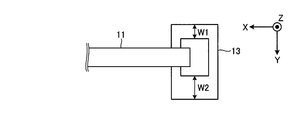
また、図6Bに示すように、枠体13の幅を左右でそれぞれ異ならせてもよい。すなわち、これまで示したコネクタ21は、上面視した場合に、端子部12の挿入方向に略平行な二辺を有する略矩形状を呈していたが、かかる二辺それぞれに対向する枠体13の幅「W1」および「W2」を、たとえば、「W1<W2」となるようにしてもよい。
なお、これは、たとえば、基板20上に複数個のコネクタ21が並設され、かつ、コネクタ21相互の間隔がまちまちである場合などに適用することができ、前述の間隔に応じて枠体13の幅を異ならせることで、接続対象となるコネクタ21を正しく選択させることができる。
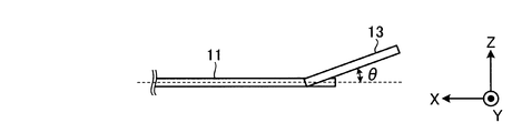
また、図6Cに示すように、ケーブル部11の延在方向(すなわち、X軸方向)に対して、枠体13が所定の傾きθを有して設けられていてもよい。この場合、枠体13が傾いている側が表側というようにあらかじめ規定しておくことで、誤接続の防止に資することができる。
なお、このように枠体13が傾きθを有していても、上述のように枠体13はロックタブ21cによって上方から押圧されるため、コネクタ21への接続時にはフラットな状態にすることができる。
上述してきたように、実施形態に係るフレキシブルケーブルは、端子部と、枠体と、パターン配線と、開口部とを備える。端子部は、配線基板上へ設けられたコネクタへ接続される。枠体は、上記端子部へ設けられる。パターン配線は、上記枠体に形成され絶縁被覆される。開口部は、上記枠体の上記パターン配線の一部を露出させる。
したがって、実施形態に係るフレキシブルケーブルによれば、電子機器の小型化を阻害することなくノイズを抑制することができる。
ところで、上述した実施形態では、フレキシブルケーブルがFPCケーブルである場合を例に挙げて説明したが、可撓性を有するならばこれに限られるものではなく、たとえば、FFC(Flexible Flat Cable)などであってもよい。
また、上述した実施形態では、コネクタがZIFコネクタである場合を例に挙げて説明したが、これに限られるものではない。たとえば、ZIFコネクタのような端子部のロック機構を備えないコネクタに適用することとしてもよい。
かかる場合、コネクタの外周を枠体が取り囲むことによって、少なくとも水平方向からの抜去力に対しては確実な抜け防止の効果を得られるとともに、ノイズ抑制についてはZIFコネクタの場合と同様の効果を得ることができる。
さらなる効果や変形例は、当業者によって容易に導き出すことができる。このため、本発明のより広範な態様は、以上のように表しかつ記述した特定の詳細および代表的な実施形態に限定されるものではない。したがって、添付の特許請求の範囲およびその均等物によって定義される総括的な発明の概念の精神または範囲から逸脱することなく、様々な変更が可能である。
1 接続機構
10 フレキシブルケーブル
11 ケーブル部
11a パターン配線
11b 絶縁フィルム
11c 切り欠き
11d 合印
12 端子部
13 枠体
13a シールドパターン
13b 絶縁フィルム
13c 開口部
20 基板
21 コネクタ
21a 挿入部
21b レバー
21c ロックタブ
22 はんだバンプ
22’ チップ部品
22’a 電極
23 グランド
10 フレキシブルケーブル
11 ケーブル部
11a パターン配線
11b 絶縁フィルム
11c 切り欠き
11d 合印
12 端子部
13 枠体
13a シールドパターン
13b 絶縁フィルム
13c 開口部
20 基板
21 コネクタ
21a 挿入部
21b レバー
21c ロックタブ
22 はんだバンプ
22’ チップ部品
22’a 電極
23 グランド
Claims (10)
- 配線基板上へ設けられたコネクタへ接続される端子部と、
前記端子部へ設けられる枠体と、
前記枠体に形成され絶縁被覆されたパターン配線と、
前記枠体の前記パターン配線の一部を露出させる開口部と
を備えることを特徴とするフレキシブルケーブル。 - 前記コネクタの近傍には、所定の高さを有し、かつ、前記配線基板のグランドと導通するグランド部材が配設されており、
前記開口部は、
前記端子部が前記コネクタへ接続された際に、該開口部によって露出される前記パターン配線の一部を前記グランド部材へ接触させるように、
前記グランド部材とが重なる部位に設けられること
を特徴とする請求項1に記載のフレキシブルケーブル。 - 前記枠体は、
前記端子部が前記コネクタへ接続された際に、該枠体の内周で前記コネクタの外周を取り囲む形状に形成されること
を特徴とする請求項1または2に記載のフレキシブルケーブル。 - 前記端子部の近傍には、該端子部の表裏または挿入方向を示す合印が設けられること
を特徴とする請求項1、2または3に記載のフレキシブルケーブル。 - 前記コネクタは、
上面視した場合に、前記端子部の挿入方向に略平行な二辺を有する略矩形状を呈しており、
前記二辺それぞれに対向する該枠体の幅は、それぞれ異なること
を特徴とする請求項3または4に記載のフレキシブルケーブル。 - 前記コネクタは、
前記配線基板へ向けて倒されることによって前記端子部と該コネクタとを固定させるレバーを具備するZIFコネクタであって、
前記枠体は、
前記レバーが倒された場合に、該レバーによって上方から押圧されることによって、前記開口部から露出された前記パターン配線の一部を前記グランド部材へ押し付けること
を特徴とする請求項2~5のいずれか一つに記載のフレキシブルケーブル。 - コネクタと、
前記コネクタの近傍に1または複数個配設され、グランドと導通するグランド部材と
を具備する配線基板と、
前記コネクタへ接続される端子部と、前記端子部へ設けられる枠体と、前記枠体に形成され絶縁被覆されたパターン配線と、前記枠体の前記パターン配線の一部を露出させる開口部とを具備するフレキシブルケーブルと
を備え、
前記端子部が前記コネクタへ接続された際に、前記開口部によって露出された前記パターン配線の一部を前記グランド部材へ接触させること
を特徴とするフレキシブルケーブルの接続機構。 - 前記グランド部材は、
はんだバンプまたはチップ部品であること
を特徴とする請求項7に記載のフレキシブルケーブルの接続機構。 - 端子部と、前記端子部へ設けられる枠体と、前記枠体に形成され絶縁被覆されたパターン配線と、前記枠体の前記パターン配線の一部を露出させる開口部とを具備するフレキシブルケーブルの前記端子部を接続するコネクタと、
前記コネクタの近傍に1または複数個配設され、グランドと導通するとともに、前記開口部によって露出された前記パターン配線の一部と接触するグランド部材と
を備えることを特徴とする配線基板。 - 請求項9に記載の配線基板を備えることを特徴とする電子機器。
Priority Applications (1)
| Application Number | Priority Date | Filing Date | Title |
|---|---|---|---|
| PCT/JP2012/065764 WO2013190664A1 (ja) | 2012-06-20 | 2012-06-20 | フレキシブルケーブル、フレキシブルケーブルの接続機構、配線基板および電子機器 |
Applications Claiming Priority (1)
| Application Number | Priority Date | Filing Date | Title |
|---|---|---|---|
| PCT/JP2012/065764 WO2013190664A1 (ja) | 2012-06-20 | 2012-06-20 | フレキシブルケーブル、フレキシブルケーブルの接続機構、配線基板および電子機器 |
Publications (1)
| Publication Number | Publication Date |
|---|---|
| WO2013190664A1 true WO2013190664A1 (ja) | 2013-12-27 |
Family
ID=49768293
Family Applications (1)
| Application Number | Title | Priority Date | Filing Date |
|---|---|---|---|
| PCT/JP2012/065764 Ceased WO2013190664A1 (ja) | 2012-06-20 | 2012-06-20 | フレキシブルケーブル、フレキシブルケーブルの接続機構、配線基板および電子機器 |
Country Status (1)
| Country | Link |
|---|---|
| WO (1) | WO2013190664A1 (ja) |
Citations (5)
| Publication number | Priority date | Publication date | Assignee | Title |
|---|---|---|---|---|
| JPH0636262U (ja) * | 1992-10-09 | 1994-05-13 | 株式会社村田製作所 | フレキシブル配線ケーブル |
| JPH0648189U (ja) * | 1992-10-07 | 1994-06-28 | 株式会社村田製作所 | フレキシブル配線シート及びコネクタ |
| JP3124813U (ja) * | 2006-06-16 | 2006-08-31 | ソニーケミカル&インフォメーションデバイス株式会社 | フレキシブルフラットケーブル |
| JP2009032462A (ja) * | 2007-07-25 | 2009-02-12 | Phoeton Corp | ワイヤーハーネス |
| JP2010192287A (ja) * | 2009-02-19 | 2010-09-02 | Sumitomo Electric Ind Ltd | 高速伝送用フレキシブルフラット高周波ケーブル端末接続構造及びその製造方法 |
-
2012
- 2012-06-20 WO PCT/JP2012/065764 patent/WO2013190664A1/ja not_active Ceased
Patent Citations (5)
| Publication number | Priority date | Publication date | Assignee | Title |
|---|---|---|---|---|
| JPH0648189U (ja) * | 1992-10-07 | 1994-06-28 | 株式会社村田製作所 | フレキシブル配線シート及びコネクタ |
| JPH0636262U (ja) * | 1992-10-09 | 1994-05-13 | 株式会社村田製作所 | フレキシブル配線ケーブル |
| JP3124813U (ja) * | 2006-06-16 | 2006-08-31 | ソニーケミカル&インフォメーションデバイス株式会社 | フレキシブルフラットケーブル |
| JP2009032462A (ja) * | 2007-07-25 | 2009-02-12 | Phoeton Corp | ワイヤーハーネス |
| JP2010192287A (ja) * | 2009-02-19 | 2010-09-02 | Sumitomo Electric Ind Ltd | 高速伝送用フレキシブルフラット高周波ケーブル端末接続構造及びその製造方法 |
Similar Documents
| Publication | Publication Date | Title |
|---|---|---|
| US8242374B2 (en) | Flexible-circuit-board cable with positioning structure for insertion | |
| CN113163595A (zh) | 覆晶薄膜、卷材和显示装置 | |
| CN108633170A (zh) | 一种印刷电路板组件及电子设备 | |
| JP2003101173A (ja) | フレキシブルプリント基板 | |
| JP2015084275A (ja) | コネクタ | |
| CN101686595B (zh) | 电子装置及其导电片 | |
| US8779292B2 (en) | Substrate and substrate bonding device using the same | |
| JP2008226786A (ja) | 電子機器 | |
| US8845360B2 (en) | Terminal connection device | |
| TWM405673U (en) | Flexible cable with electromagnetic shielding connector structure | |
| JP2009200015A (ja) | フレキシブル配線基板用コネクタおよび電子装置 | |
| CN113179579A (zh) | 电路板和电子设备 | |
| US20110147075A1 (en) | Electronic Apparatus | |
| TW201725941A (zh) | 電路板組合 | |
| WO2013190664A1 (ja) | フレキシブルケーブル、フレキシブルケーブルの接続機構、配線基板および電子機器 | |
| JP5119852B2 (ja) | フレキシブル配線基板 | |
| CN116345207A (zh) | 压接邦定结构、连接器、电子模组及电子设备 | |
| US11899498B2 (en) | Flexible printed circuit and display apparatus | |
| JP2010092740A (ja) | 基板用電線接続構造体 | |
| JP4020050B2 (ja) | ケーブル接続部 | |
| JP5170198B2 (ja) | 配線基板付ケーブルアセンブリ | |
| CN105555020A (zh) | 软硬结合板及终端 | |
| JP4055012B2 (ja) | 電子機器 | |
| JP2012064737A (ja) | 電子部品のシールド構造、シールド部材及びこれを備える電子機器 | |
| US20170238414A1 (en) | Flexible printed circuit and electronic apparatus |
Legal Events
| Date | Code | Title | Description |
|---|---|---|---|
| 121 | Ep: the epo has been informed by wipo that ep was designated in this application |
Ref document number: 12879426 Country of ref document: EP Kind code of ref document: A1 |
|
| NENP | Non-entry into the national phase |
Ref country code: DE |
|
| 122 | Ep: pct application non-entry in european phase |
Ref document number: 12879426 Country of ref document: EP Kind code of ref document: A1 |
|
| NENP | Non-entry into the national phase |
Ref country code: JP |