WO2013175697A1 - Nitride semiconductor light emitting device - Google Patents
Nitride semiconductor light emitting device Download PDFInfo
- Publication number
- WO2013175697A1 WO2013175697A1 PCT/JP2013/002346 JP2013002346W WO2013175697A1 WO 2013175697 A1 WO2013175697 A1 WO 2013175697A1 JP 2013002346 W JP2013002346 W JP 2013002346W WO 2013175697 A1 WO2013175697 A1 WO 2013175697A1
- Authority
- WO
- WIPO (PCT)
- Prior art keywords
- nitride semiconductor
- semiconductor light
- light emitting
- emitting device
- submount
- Prior art date
Links
Images


Classifications
-
- H—ELECTRICITY
- H01—ELECTRIC ELEMENTS
- H01L—SEMICONDUCTOR DEVICES NOT COVERED BY CLASS H10
- H01L33/00—Semiconductor devices with at least one potential-jump barrier or surface barrier specially adapted for light emission; Processes or apparatus specially adapted for the manufacture or treatment thereof or of parts thereof; Details thereof
- H01L33/02—Semiconductor devices with at least one potential-jump barrier or surface barrier specially adapted for light emission; Processes or apparatus specially adapted for the manufacture or treatment thereof or of parts thereof; Details thereof characterised by the semiconductor bodies
- H01L33/12—Semiconductor devices with at least one potential-jump barrier or surface barrier specially adapted for light emission; Processes or apparatus specially adapted for the manufacture or treatment thereof or of parts thereof; Details thereof characterised by the semiconductor bodies with a stress relaxation structure, e.g. buffer layer
-
- B—PERFORMING OPERATIONS; TRANSPORTING
- B82—NANOTECHNOLOGY
- B82Y—SPECIFIC USES OR APPLICATIONS OF NANOSTRUCTURES; MEASUREMENT OR ANALYSIS OF NANOSTRUCTURES; MANUFACTURE OR TREATMENT OF NANOSTRUCTURES
- B82Y20/00—Nanooptics, e.g. quantum optics or photonic crystals
-
- H—ELECTRICITY
- H01—ELECTRIC ELEMENTS
- H01L—SEMICONDUCTOR DEVICES NOT COVERED BY CLASS H10
- H01L33/00—Semiconductor devices with at least one potential-jump barrier or surface barrier specially adapted for light emission; Processes or apparatus specially adapted for the manufacture or treatment thereof or of parts thereof; Details thereof
- H01L33/02—Semiconductor devices with at least one potential-jump barrier or surface barrier specially adapted for light emission; Processes or apparatus specially adapted for the manufacture or treatment thereof or of parts thereof; Details thereof characterised by the semiconductor bodies
- H01L33/04—Semiconductor devices with at least one potential-jump barrier or surface barrier specially adapted for light emission; Processes or apparatus specially adapted for the manufacture or treatment thereof or of parts thereof; Details thereof characterised by the semiconductor bodies with a quantum effect structure or superlattice, e.g. tunnel junction
- H01L33/06—Semiconductor devices with at least one potential-jump barrier or surface barrier specially adapted for light emission; Processes or apparatus specially adapted for the manufacture or treatment thereof or of parts thereof; Details thereof characterised by the semiconductor bodies with a quantum effect structure or superlattice, e.g. tunnel junction within the light emitting region, e.g. quantum confinement structure or tunnel barrier
-
- H—ELECTRICITY
- H01—ELECTRIC ELEMENTS
- H01L—SEMICONDUCTOR DEVICES NOT COVERED BY CLASS H10
- H01L33/00—Semiconductor devices with at least one potential-jump barrier or surface barrier specially adapted for light emission; Processes or apparatus specially adapted for the manufacture or treatment thereof or of parts thereof; Details thereof
- H01L33/02—Semiconductor devices with at least one potential-jump barrier or surface barrier specially adapted for light emission; Processes or apparatus specially adapted for the manufacture or treatment thereof or of parts thereof; Details thereof characterised by the semiconductor bodies
- H01L33/14—Semiconductor devices with at least one potential-jump barrier or surface barrier specially adapted for light emission; Processes or apparatus specially adapted for the manufacture or treatment thereof or of parts thereof; Details thereof characterised by the semiconductor bodies with a carrier transport control structure, e.g. highly-doped semiconductor layer or current-blocking structure
- H01L33/145—Semiconductor devices with at least one potential-jump barrier or surface barrier specially adapted for light emission; Processes or apparatus specially adapted for the manufacture or treatment thereof or of parts thereof; Details thereof characterised by the semiconductor bodies with a carrier transport control structure, e.g. highly-doped semiconductor layer or current-blocking structure with a current-blocking structure
-
- H—ELECTRICITY
- H01—ELECTRIC ELEMENTS
- H01L—SEMICONDUCTOR DEVICES NOT COVERED BY CLASS H10
- H01L33/00—Semiconductor devices with at least one potential-jump barrier or surface barrier specially adapted for light emission; Processes or apparatus specially adapted for the manufacture or treatment thereof or of parts thereof; Details thereof
- H01L33/02—Semiconductor devices with at least one potential-jump barrier or surface barrier specially adapted for light emission; Processes or apparatus specially adapted for the manufacture or treatment thereof or of parts thereof; Details thereof characterised by the semiconductor bodies
- H01L33/16—Semiconductor devices with at least one potential-jump barrier or surface barrier specially adapted for light emission; Processes or apparatus specially adapted for the manufacture or treatment thereof or of parts thereof; Details thereof characterised by the semiconductor bodies with a particular crystal structure or orientation, e.g. polycrystalline, amorphous or porous
-
- H—ELECTRICITY
- H01—ELECTRIC ELEMENTS
- H01L—SEMICONDUCTOR DEVICES NOT COVERED BY CLASS H10
- H01L33/00—Semiconductor devices with at least one potential-jump barrier or surface barrier specially adapted for light emission; Processes or apparatus specially adapted for the manufacture or treatment thereof or of parts thereof; Details thereof
- H01L33/02—Semiconductor devices with at least one potential-jump barrier or surface barrier specially adapted for light emission; Processes or apparatus specially adapted for the manufacture or treatment thereof or of parts thereof; Details thereof characterised by the semiconductor bodies
- H01L33/26—Materials of the light emitting region
- H01L33/30—Materials of the light emitting region containing only elements of group III and group V of the periodic system
- H01L33/32—Materials of the light emitting region containing only elements of group III and group V of the periodic system containing nitrogen
-
- H—ELECTRICITY
- H01—ELECTRIC ELEMENTS
- H01L—SEMICONDUCTOR DEVICES NOT COVERED BY CLASS H10
- H01L33/00—Semiconductor devices with at least one potential-jump barrier or surface barrier specially adapted for light emission; Processes or apparatus specially adapted for the manufacture or treatment thereof or of parts thereof; Details thereof
- H01L33/48—Semiconductor devices with at least one potential-jump barrier or surface barrier specially adapted for light emission; Processes or apparatus specially adapted for the manufacture or treatment thereof or of parts thereof; Details thereof characterised by the semiconductor body packages
- H01L33/483—Containers
-
- H—ELECTRICITY
- H01—ELECTRIC ELEMENTS
- H01L—SEMICONDUCTOR DEVICES NOT COVERED BY CLASS H10
- H01L33/00—Semiconductor devices with at least one potential-jump barrier or surface barrier specially adapted for light emission; Processes or apparatus specially adapted for the manufacture or treatment thereof or of parts thereof; Details thereof
- H01L33/48—Semiconductor devices with at least one potential-jump barrier or surface barrier specially adapted for light emission; Processes or apparatus specially adapted for the manufacture or treatment thereof or of parts thereof; Details thereof characterised by the semiconductor body packages
- H01L33/64—Heat extraction or cooling elements
-
- H—ELECTRICITY
- H01—ELECTRIC ELEMENTS
- H01S—DEVICES USING THE PROCESS OF LIGHT AMPLIFICATION BY STIMULATED EMISSION OF RADIATION [LASER] TO AMPLIFY OR GENERATE LIGHT; DEVICES USING STIMULATED EMISSION OF ELECTROMAGNETIC RADIATION IN WAVE RANGES OTHER THAN OPTICAL
- H01S5/00—Semiconductor lasers
- H01S5/02—Structural details or components not essential to laser action
- H01S5/0206—Substrates, e.g. growth, shape, material, removal or bonding
-
- H—ELECTRICITY
- H01—ELECTRIC ELEMENTS
- H01S—DEVICES USING THE PROCESS OF LIGHT AMPLIFICATION BY STIMULATED EMISSION OF RADIATION [LASER] TO AMPLIFY OR GENERATE LIGHT; DEVICES USING STIMULATED EMISSION OF ELECTROMAGNETIC RADIATION IN WAVE RANGES OTHER THAN OPTICAL
- H01S5/00—Semiconductor lasers
- H01S5/02—Structural details or components not essential to laser action
- H01S5/022—Mountings; Housings
- H01S5/0235—Method for mounting laser chips
- H01S5/02355—Fixing laser chips on mounts
- H01S5/0236—Fixing laser chips on mounts using an adhesive
-
- H—ELECTRICITY
- H01—ELECTRIC ELEMENTS
- H01S—DEVICES USING THE PROCESS OF LIGHT AMPLIFICATION BY STIMULATED EMISSION OF RADIATION [LASER] TO AMPLIFY OR GENERATE LIGHT; DEVICES USING STIMULATED EMISSION OF ELECTROMAGNETIC RADIATION IN WAVE RANGES OTHER THAN OPTICAL
- H01S5/00—Semiconductor lasers
- H01S5/02—Structural details or components not essential to laser action
- H01S5/022—Mountings; Housings
- H01S5/0235—Method for mounting laser chips
- H01S5/02355—Fixing laser chips on mounts
- H01S5/0237—Fixing laser chips on mounts by soldering
-
- H—ELECTRICITY
- H01—ELECTRIC ELEMENTS
- H01S—DEVICES USING THE PROCESS OF LIGHT AMPLIFICATION BY STIMULATED EMISSION OF RADIATION [LASER] TO AMPLIFY OR GENERATE LIGHT; DEVICES USING STIMULATED EMISSION OF ELECTROMAGNETIC RADIATION IN WAVE RANGES OTHER THAN OPTICAL
- H01S5/00—Semiconductor lasers
- H01S5/02—Structural details or components not essential to laser action
- H01S5/024—Arrangements for thermal management
- H01S5/02469—Passive cooling, e.g. where heat is removed by the housing as a whole or by a heat pipe without any active cooling element like a TEC
-
- H—ELECTRICITY
- H01—ELECTRIC ELEMENTS
- H01S—DEVICES USING THE PROCESS OF LIGHT AMPLIFICATION BY STIMULATED EMISSION OF RADIATION [LASER] TO AMPLIFY OR GENERATE LIGHT; DEVICES USING STIMULATED EMISSION OF ELECTROMAGNETIC RADIATION IN WAVE RANGES OTHER THAN OPTICAL
- H01S5/00—Semiconductor lasers
- H01S5/02—Structural details or components not essential to laser action
- H01S5/024—Arrangements for thermal management
- H01S5/02476—Heat spreaders, i.e. improving heat flow between laser chip and heat dissipating elements
-
- H—ELECTRICITY
- H01—ELECTRIC ELEMENTS
- H01S—DEVICES USING THE PROCESS OF LIGHT AMPLIFICATION BY STIMULATED EMISSION OF RADIATION [LASER] TO AMPLIFY OR GENERATE LIGHT; DEVICES USING STIMULATED EMISSION OF ELECTROMAGNETIC RADIATION IN WAVE RANGES OTHER THAN OPTICAL
- H01S5/00—Semiconductor lasers
- H01S5/04—Processes or apparatus for excitation, e.g. pumping, e.g. by electron beams
- H01S5/042—Electrical excitation ; Circuits therefor
- H01S5/0425—Electrodes, e.g. characterised by the structure
- H01S5/04252—Electrodes, e.g. characterised by the structure characterised by the material
-
- H—ELECTRICITY
- H01—ELECTRIC ELEMENTS
- H01S—DEVICES USING THE PROCESS OF LIGHT AMPLIFICATION BY STIMULATED EMISSION OF RADIATION [LASER] TO AMPLIFY OR GENERATE LIGHT; DEVICES USING STIMULATED EMISSION OF ELECTROMAGNETIC RADIATION IN WAVE RANGES OTHER THAN OPTICAL
- H01S5/00—Semiconductor lasers
- H01S5/20—Structure or shape of the semiconductor body to guide the optical wave ; Confining structures perpendicular to the optical axis, e.g. index or gain guiding, stripe geometry, broad area lasers, gain tailoring, transverse or lateral reflectors, special cladding structures, MQW barrier reflection layers
- H01S5/2004—Confining in the direction perpendicular to the layer structure
- H01S5/2009—Confining in the direction perpendicular to the layer structure by using electron barrier layers
-
- H—ELECTRICITY
- H01—ELECTRIC ELEMENTS
- H01S—DEVICES USING THE PROCESS OF LIGHT AMPLIFICATION BY STIMULATED EMISSION OF RADIATION [LASER] TO AMPLIFY OR GENERATE LIGHT; DEVICES USING STIMULATED EMISSION OF ELECTROMAGNETIC RADIATION IN WAVE RANGES OTHER THAN OPTICAL
- H01S5/00—Semiconductor lasers
- H01S5/30—Structure or shape of the active region; Materials used for the active region
- H01S5/32—Structure or shape of the active region; Materials used for the active region comprising PN junctions, e.g. hetero- or double- heterostructures
- H01S5/323—Structure or shape of the active region; Materials used for the active region comprising PN junctions, e.g. hetero- or double- heterostructures in AIIIBV compounds, e.g. AlGaAs-laser, InP-based laser
- H01S5/32308—Structure or shape of the active region; Materials used for the active region comprising PN junctions, e.g. hetero- or double- heterostructures in AIIIBV compounds, e.g. AlGaAs-laser, InP-based laser emitting light at a wavelength less than 900 nm
- H01S5/32341—Structure or shape of the active region; Materials used for the active region comprising PN junctions, e.g. hetero- or double- heterostructures in AIIIBV compounds, e.g. AlGaAs-laser, InP-based laser emitting light at a wavelength less than 900 nm blue laser based on GaN or GaP
-
- H—ELECTRICITY
- H01—ELECTRIC ELEMENTS
- H01S—DEVICES USING THE PROCESS OF LIGHT AMPLIFICATION BY STIMULATED EMISSION OF RADIATION [LASER] TO AMPLIFY OR GENERATE LIGHT; DEVICES USING STIMULATED EMISSION OF ELECTROMAGNETIC RADIATION IN WAVE RANGES OTHER THAN OPTICAL
- H01S5/00—Semiconductor lasers
- H01S5/30—Structure or shape of the active region; Materials used for the active region
- H01S5/34—Structure or shape of the active region; Materials used for the active region comprising quantum well or superlattice structures, e.g. single quantum well [SQW] lasers, multiple quantum well [MQW] lasers or graded index separate confinement heterostructure [GRINSCH] lasers
- H01S5/343—Structure or shape of the active region; Materials used for the active region comprising quantum well or superlattice structures, e.g. single quantum well [SQW] lasers, multiple quantum well [MQW] lasers or graded index separate confinement heterostructure [GRINSCH] lasers in AIIIBV compounds, e.g. AlGaAs-laser, InP-based laser
- H01S5/34333—Structure or shape of the active region; Materials used for the active region comprising quantum well or superlattice structures, e.g. single quantum well [SQW] lasers, multiple quantum well [MQW] lasers or graded index separate confinement heterostructure [GRINSCH] lasers in AIIIBV compounds, e.g. AlGaAs-laser, InP-based laser with a well layer based on Ga(In)N or Ga(In)P, e.g. blue laser
-
- H—ELECTRICITY
- H01—ELECTRIC ELEMENTS
- H01L—SEMICONDUCTOR DEVICES NOT COVERED BY CLASS H10
- H01L2224/00—Indexing scheme for arrangements for connecting or disconnecting semiconductor or solid-state bodies and methods related thereto as covered by H01L24/00
- H01L2224/01—Means for bonding being attached to, or being formed on, the surface to be connected, e.g. chip-to-package, die-attach, "first-level" interconnects; Manufacturing methods related thereto
- H01L2224/42—Wire connectors; Manufacturing methods related thereto
- H01L2224/47—Structure, shape, material or disposition of the wire connectors after the connecting process
- H01L2224/48—Structure, shape, material or disposition of the wire connectors after the connecting process of an individual wire connector
- H01L2224/4805—Shape
- H01L2224/4809—Loop shape
- H01L2224/48091—Arched
-
- H—ELECTRICITY
- H01—ELECTRIC ELEMENTS
- H01L—SEMICONDUCTOR DEVICES NOT COVERED BY CLASS H10
- H01L33/00—Semiconductor devices with at least one potential-jump barrier or surface barrier specially adapted for light emission; Processes or apparatus specially adapted for the manufacture or treatment thereof or of parts thereof; Details thereof
- H01L33/48—Semiconductor devices with at least one potential-jump barrier or surface barrier specially adapted for light emission; Processes or apparatus specially adapted for the manufacture or treatment thereof or of parts thereof; Details thereof characterised by the semiconductor body packages
- H01L33/64—Heat extraction or cooling elements
- H01L33/641—Heat extraction or cooling elements characterized by the materials
-
- H—ELECTRICITY
- H01—ELECTRIC ELEMENTS
- H01S—DEVICES USING THE PROCESS OF LIGHT AMPLIFICATION BY STIMULATED EMISSION OF RADIATION [LASER] TO AMPLIFY OR GENERATE LIGHT; DEVICES USING STIMULATED EMISSION OF ELECTROMAGNETIC RADIATION IN WAVE RANGES OTHER THAN OPTICAL
- H01S2304/00—Special growth methods for semiconductor lasers
- H01S2304/04—MOCVD or MOVPE
-
- H—ELECTRICITY
- H01—ELECTRIC ELEMENTS
- H01S—DEVICES USING THE PROCESS OF LIGHT AMPLIFICATION BY STIMULATED EMISSION OF RADIATION [LASER] TO AMPLIFY OR GENERATE LIGHT; DEVICES USING STIMULATED EMISSION OF ELECTROMAGNETIC RADIATION IN WAVE RANGES OTHER THAN OPTICAL
- H01S5/00—Semiconductor lasers
- H01S5/02—Structural details or components not essential to laser action
- H01S5/022—Mountings; Housings
- H01S5/02208—Mountings; Housings characterised by the shape of the housings
- H01S5/02212—Can-type, e.g. TO-CAN housings with emission along or parallel to symmetry axis
-
- H—ELECTRICITY
- H01—ELECTRIC ELEMENTS
- H01S—DEVICES USING THE PROCESS OF LIGHT AMPLIFICATION BY STIMULATED EMISSION OF RADIATION [LASER] TO AMPLIFY OR GENERATE LIGHT; DEVICES USING STIMULATED EMISSION OF ELECTROMAGNETIC RADIATION IN WAVE RANGES OTHER THAN OPTICAL
- H01S5/00—Semiconductor lasers
- H01S5/02—Structural details or components not essential to laser action
- H01S5/022—Mountings; Housings
- H01S5/0233—Mounting configuration of laser chips
- H01S5/02345—Wire-bonding
Definitions
- the present disclosure relates to a structure of a light emitting device, in particular, a nitride semiconductor light emitting device having a large light output used for a light source such as a projector or a liquid crystal backlight.
- a nitride semiconductor light emitting device in which a nitride semiconductor light emitting element such as a light emitting diode using a nitride semiconductor or a semiconductor laser is mounted has attracted attention.
- a light source combining a nitride semiconductor light-emitting device and a phosphor can emit white light with high light output, and is smaller and more efficient than conventional incandescent bulbs, fluorescent lamps, and high-pressure mercury lamps. Since it has a feature such as long life, it is rapidly being replaced as a light source for display devices such as projectors and liquid crystal backlights.
- a nitride semiconductor light emitting device having a waveguide represented by a nitride semiconductor laser
- a nitride semiconductor light emitting device having a waveguide represented by a nitride semiconductor laser
- excellent directivity indicating the direction of light emission.
- practical application of a laser scribing apparatus and a laser annealing apparatus using a nitride semiconductor light emitting device as a light source is proceeding. Since the light source used in these devices requires a high light output in the watt class with an optical output of 1 watt or more, the nitride semiconductor light emitting device is also required to have a high output.
- a light-emitting device such as a nitride semiconductor light-emitting device emits light by injecting electrons and holes (electron-hole pairs) into an active layer composed of quantum wells and recombining them. At this time, the energy that has not been converted to light becomes Joule heat, which raises the temperature of the element.
- it is necessary to increase the amount of current (electrons and holes) to be injected.
- the increase in current increases the heat generation of the nitride semiconductor light emitting element. When the element temperature rises due to this heat generation, a part of electrons or holes is not injected into the active layer and an overflow phenomenon (a phenomenon called carrier overflow) occurs.
- Patent Document 1 shows a structure of a conventional nitride semiconductor laser.
- FIG. 17A shows the structure.
- FIG. 17B shows the conduction band side of the energy band gap.
- the n-AlGaN cladding layer 1003, the InGaN active layer 1005, and the p-AlGaN electron overflow are suppressed on the GaN substrate 1001 and the n-GaN layer 1002.
- It has a stacked structure including a layer 1010 (this layer is called an electron blocking layer in this specification), a p-AlGaN cladding layer 1011, and a p-GaN contact layer 1012.
- the electron block layer 1010 is a layer provided to prevent electrons injected from the n-GaN layer 1002 from passing through the active layer 1005 and overflowing to the p-AlGaN cladding layer 1011. As shown in FIG. 17B, the electron block layer 1010 has a larger energy band gap than the surrounding layers. For the electron block layer 1010, an AlGaN layer having a large Al composition is used in order to increase the energy band gap.
- a piezoelectric field may be generated due to lattice mismatch distortion.
- the lattice constant of the p-AlGaN electron block layer 1010 described above has a smaller value than the lattice constant of the GaN substrate 1001. From this point, tensile strain is generated in the p-AlGaN electron block layer 1010, and piezoelectrolysis is generated by the strain. The electron confinement effect by the p-AlGaN electron block layer is reduced by this piezo electric field.
- Patent Document 2 shows that the effective barrier height against electrons is reduced by the piezoelectric field. Therefore, Patent Document 2 proposes a method of increasing the thickness of the p-AlGaN block layer that confines electrons. When the thickness of the AlGaN layer is increased, elastic lattice mismatch strain is relaxed due to the generation of dislocations and cracks. This reduces the piezo electric field due to lattice mismatch distortion, resulting in an increase in barrier height for electrons in the conduction band.
- An object of the present invention is to provide a nitride semiconductor light emitting device capable of reducing the influence of a piezoelectric field without plastic deformation and effectively reducing the overflow of carriers in the nitride semiconductor light emitting element. That is, it is possible to provide a configuration of a nitride semiconductor light emitting device that can operate at a higher output.
- the inventors of the present application paid attention to the relationship between the piezoelectric field formed in the electron block layer in the nitride semiconductor light emitting element and the configuration of the nitride semiconductor light emitting device mounted with the nitride semiconductor light emitting element. Specifically, it has been found that by controlling the coefficient of thermal expansion of the submount on which the nitride semiconductor light emitting element is mounted, carrier overflow can be effectively suppressed even when the temperature of the element rises. As a result, the inventors have found a nitride semiconductor light emitting device configuration that increases the light output.
- the nitride semiconductor light emitting device of the present disclosure includes a nitride semiconductor light emitting element having a configuration in which a nitride semiconductor multilayer film is stacked on a nitride semiconductor substrate having a polar surface or a semipolar surface on the surface;
- the nitride semiconductor multilayer film includes an electron block layer, and the lattice constant of the electron block layer is smaller than the lattice constant of the nitride semiconductor substrate,
- the mounting portion has at least a first mounting portion base material, and the first mounting portion base material is located on the side on which the nitride semiconductor light emitting element is mounted, and the heat of the first mounting portion base material is The expansion coefficient is smaller than the thermal expansion coefficient of the nitride semiconductor multilayer film, and the thermal conductivity of the first mounting portion base material is larger than the thermal conductivity of the nitride
- the mounting portion may be configured only by the first mounting portion base material.
- the first mounting portion base material may have a thermal expansion coefficient of 4 ⁇ 10 ⁇ 6 K ⁇ 1 or lower, and the first mounting portion base material may have a thermal conductivity of 300 W / mK or higher.
- the mounting portion includes a second mounting portion base material made of a material different from that of the first mounting portion base material and joined to the first mounting portion base material. May be located closer to the nitride semiconductor light emitting element than the second mounting portion base material.
- the first mounting portion base material is made of a high-cost material, the above-described effects can be realized while reducing the amount of use.
- the first mounting portion base material may be made of any one of high thermal conductivity SiC ceramic, CVD-diamond, or a composite material of diamond and copper.
- the first mounting portion base material may have a thermal expansion coefficient of 3 ⁇ 10 ⁇ 6 K ⁇ 1 or less.
- the Joule heat of the nitride semiconductor light emitting element may be 3 W or more.
- the nitride semiconductor light emitting device of the present disclosure is particularly effective when the light output is high and the heat generation amount is large.
- the nitride semiconductor light emitting element may be a semiconductor laser element.
- the confinement of injected carriers in the active layer greatly affects the light emission characteristics. Therefore, this configuration can greatly improve the high output characteristics of the semiconductor laser.
- the nitride semiconductor light emitting element may be a light emitting diode.
- This configuration makes it possible to obtain a high light output effectively when driving a large current with a temperature rise.
- thermal expansion coefficient of the first mounting portion base material may be smaller than the thermal expansion coefficient of the second mounting portion base material.
- the volume of the first mounting portion base material is preferably larger than the volume of the nitride semiconductor light emitting device.
- the mounting portion may be a submount mounted on another element mounting base or base material.
- a nitride semiconductor light emitting element can be mounted on a submount that can be easily formed into a rectangular parallelepiped, and this can be mounted on another element mounting base, base material, stem, or the like. . Therefore, it is possible to cope with the case where the workability of the material of the mounting portion is low.
- a nitride semiconductor light emitting device that can effectively suppress the overflow of carriers and increase the light output even when the temperature of the element rises due to energization at low cost.
- FIG. 1 is a cross-sectional view illustrating the configuration of the nitride semiconductor light emitting device according to the first embodiment.
- FIG. 2 is a top view illustrating the configuration of the nitride semiconductor light emitting device according to the first embodiment. It is.
- FIG. 3 is a cross-sectional view illustrating the configuration of the nitride semiconductor light emitting device and the submount according to the first embodiment.
- FIG. 4 is a top view illustrating the configuration of the nitride semiconductor light emitting device used for verifying the effect of the present invention.
- FIG. 5A is a cross-sectional view illustrating the configuration of the nitride semiconductor light-emitting element, and FIG.
- FIG. 5B is a cross-sectional view illustrating band lineup when the nitride semiconductor light-emitting element is energized.
- FIG. 6A is a cross-sectional view illustrating the configuration of a nitride semiconductor light-emitting device
- FIG. 6B is a cross-sectional view illustrating the band lineup of the nitride semiconductor light-emitting device.
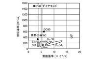
- FIG. 7 is a diagram showing the relationship between the thermal expansion coefficient and the thermal conductivity of a material applicable to the submount material of the nitride semiconductor light emitting device.
- FIG. 8 is a diagram for explaining the thermal expansion of the submount and nitride semiconductor light emitting element used in the nitride semiconductor light emitting device when the temperature rises.
- FIG. 9 is a diagram showing current-light output characteristics of the nitride semiconductor light emitting device.
- FIG. 10 is a diagram comparing the measured value and the calculated value of the maximum light output of the nitride semiconductor light emitting device.
- FIG. 11 is a top view illustrating the configuration of the nitride semiconductor light emitting device of the second embodiment.
- FIG. 12 is a cross-sectional view illustrating the configuration of the nitride semiconductor light emitting device of the second embodiment.
- FIG. 13 is a cross-sectional view illustrating the configuration of the nitride semiconductor light emitting device of the third embodiment.
- FIG. 14 is a top view illustrating the configuration of the nitride semiconductor light emitting device of the third embodiment.
- FIG. 15 is a cross-sectional view illustrating the configuration of the nitride semiconductor light emitting device of the fourth embodiment.
- FIG. 16 is a cross-sectional view illustrating a configuration of a nitride semiconductor light emitting device according to a modification of the fourth embodiment.
- 7A and 7B are diagrams showing a conventional nitride semiconductor light emitting device.
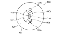
- FIG. 1 and FIG. 2 illustrate the configuration of an exemplary nitride semiconductor light emitting device 300 of this embodiment.
- FIG. 1 is a cross-sectional view of a nitride semiconductor light emitting device
- FIG. 2 is a top view of the nitride semiconductor light emitting device viewed from the light emitting direction (upper side in FIG. 1).
- the nitride semiconductor light emitting device 300 of this embodiment includes, for example, a nitride semiconductor light emitting element 310 that emits laser light having a dominant wavelength of 390 nm to 550 nm, a submount 311 on which the nitride semiconductor light emitting element 310 is mounted, and a stem. 120 and a cap 130.
- the stem 120 includes a base 121 and an element mounting base 122, and ground leads 123a, leads 123b and 123c.
- the nitride semiconductor light emitting device 310 and the submount 311 are bonded to the device mounting base 122.
- the nitride semiconductor light emitting device 310 is electrically connected to the leads 123b and 123c by bonding wires 140b and 140c.
- the positive electrode is connected to the lead 123b from the p electrode on the upper surface of the nitride semiconductor light emitting device 310 by the bonding wire 140b.
- the negative electrode is connected to the lead 123c from the first electrode formed on the surface of the submount 311 by a bonding wire 140c.
- the cap 130 includes a cover 131 having an opening 131a and a light extraction window 132. The cap 130 is welded to the stem base 121. With this configuration, the nitride semiconductor light emitting device 310 is hermetically sealed.
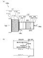
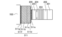
- FIG. 3 shows a detailed stacked structure of the nitride semiconductor light emitting device 310 and the submount 311.
- FIG. 3 shows a detailed stacked structure of the nitride semiconductor light emitting device 310 and the submount 311.
- a typical structure and manufacturing method of the nitride semiconductor light emitting device 310 will be described.
- the nitride semiconductor light emitting device 310 is constituted by a nitride semiconductor multilayer film formed on a nitride semiconductor substrate 201, which is an n-GaN (0001) substrate, by metal organic chemical vapor deposition (MOCVD).
- a nitride semiconductor substrate 201 includes three types of layers: a clad layer 202 made of n-AlGaN, a guide layer made of n-GaN / InGaN multiple quantum wells / a guide layer made of p-GaN.
- An active layer 203, an AlGaN electron blocking layer 204 having an Al composition ratio as high as 15 to 30%, a clad layer 205 made of p-AlGaN, and a contact layer 206 made of p-GaN are sequentially stacked.
- the plane orientation of the surface of the nitride semiconductor substrate 201 is not limited to (0001), but may include a polar or semipolar plane.
- the composition of the AlGaN electron blocking layer 204 is not limited to the above-described composition, and it is sufficient that the lattice constant is smaller than that of the substrate of the nitride semiconductor light emitting device.
- one or a plurality of ridge-type waveguides are formed using a dry etching process. Further, a p-ohmic electrode 210 made of, for example, Pd / Pt / Au is formed on the surface of the contact layer 206, and an n-ohmic electrode 211 made of, for example, Ti / Pt / Au is formed on the back surface of the nitride semiconductor substrate 201. Is formed. Note that, when the ridge-type waveguide is cleaved to a length of, for example, 800 ⁇ m, a Fabry-Perot resonator is formed and functions as a laser structure.
- the submount 311 includes a first submount base material 311a and a second submount base material 311b.
- a second submount substrate 311b for example, an AlN ceramic that can be manufactured at a relatively low cost can be used.
- diamond can be deposited on the surface of the second submount base material 311b by a CVD method to form the first submount base material 311a, and the submount 311 having a two-layer structure can be configured.
- the thermal conductivity of the submount can be increased and the thermal expansion coefficient can be set small.
- a first bonding portion 311e made of, for example, AuSn eutectic solder is formed, whereby the submount 311 and the nitride semiconductor light emitting element 310 are bonded.
- a second bonding portion 311 g made of AuSn eutectic solder is formed, and thereby the submount 311 and the element mounting base 122 of the stem 120 are bonded to each other. ing.
- the thickness of the first submount base material 311a and the second submount base material 311b is, for example, 10 times or more compared to the thickness of the first electrode 311d and the second electrode 311f, respectively.
- the thermal expansion coefficient of the submount 311 it sets so that the thermal expansion coefficient of the two submount base materials 311a and 311b may become dominant.
- the above is the configuration of the nitride semiconductor light emitting device of this embodiment. When the nitride semiconductor light emitting device of this embodiment was operated, carrier overflow could be effectively suppressed even when the temperature of the element increased due to energization. As a result, we succeeded in increasing the light output.
- FIG. 4 is a diagram showing a nitride semiconductor light emitting device 100 manufactured by the present inventors in order to verify the effect of the present embodiment.
- the shape and components of the nitride semiconductor light emitting device 100 are the same as those of the nitride semiconductor light emitting device 300 shown in FIGS. 1 and 2, and in FIG. 4, the cap 130 is omitted and a top view as seen from the light emitting direction. It is shown.
- FIGS. 5A and 5B are diagrams showing a detailed structure in the vicinity of the nitride semiconductor light emitting element 110 of the nitride semiconductor light emitting device 100 and a configuration of the energy band gap (hereinafter referred to as band line up). It is.
- the structure of the nitride semiconductor light emitting device 110 is the same as that of the nitride semiconductor light emitting device 310 of FIG. 3 except that the submount 111 has only a single submount substrate 111a.
- FIG. 6A and FIG. 6B are diagrams for explaining the function of the nitride semiconductor light emitting device 100a.
- the nitride semiconductor light emitting device 100a is the same as the nitride semiconductor light emitting device 100 of FIGS. 5A and 5B except for the material of the submount substrate 111a.
- Table 1 is a list of characteristics of materials applicable to the submount materials described later.
- FIG. 7 is a diagram showing the characteristics of the materials shown in Table 1.
- Table 2 is a list of characteristics of the submount materials examined in this embodiment.
- FIG. 8 is a calculation result for explaining the effect of the nitride semiconductor light emitting device of this embodiment.
- Table 3 is a list of calculation results showing the effects of the present embodiment.
- FIGS. 9 and 10 are diagrams showing experimental results for explaining the effect of the nitride semiconductor light emitting device 100 of the present embodiment.
- Table 4 is a list of experimental results of nitride semiconductor devices that explain the effects of this embodiment.
- the submount 111 is formed using a submount substrate 111a made of diamond formed using, for example, SiC ceramic or CVD (Chemical Vapor Deposition).
- a first electrode 111d and a second electrode having a metal laminated structure in which Ti is laminated to a thickness of 0.1 ⁇ m, Pt is 0.2 ⁇ m, and Au is 0.2 ⁇ m.
- An electrode 111f is formed.
- a first bonding portion 111e made of, for example, AuSn eutectic solder is formed, whereby the submount base material 111a and the nitride semiconductor light emitting device 110 are bonded. Yes.
- a second bonding portion 111g which is AuSn eutectic solder, is formed, thereby bonding the submount substrate 111a and the element mounting base 122 of the stem 120 to each other. Has been done.
- the thickness of the submount substrate 111a is set to be, for example, 20 times or more than the thickness of the first electrode 111d and the second electrode 111f.
- the thermal expansion coefficient of the submount 111 is set so that the thermal expansion coefficient of the submount substrate 111a is dominant.
- FIG. 5 (b) shows a band lineup of the nitride semiconductor light emitting device 110 in FIG. 5 (a).
- FIGS. 6A and 6B are a detailed laminated structure and band lineup of a comparative nitride semiconductor light emitting device 100a, and the function of the nitride semiconductor light emitting device of this embodiment will be described. Use for.
- the nitride semiconductor light emitting device 100a is different from the nitride semiconductor light emitting device 100 in the material constituting the submount base material 111a, and the submount base material 111a and the nitride semiconductor light emitting element 110 have the same thermal expansion coefficient. Is set to Therefore, the stress applied to the nitride semiconductor light emitting element 110 in the nitride semiconductor light emitting device 100a is different from the stress applied to the nitride semiconductor light emitting element 110 in the nitride semiconductor light emitting device 100.
- the direction and magnitude of the strain 221a generated in the electron block layer 204 are qualitatively shown in FIG. 6A using arrows.
- the direction of the arrow indicates the direction of distortion
- the length of the arrow indicates the magnitude of distortion.
- the lattice constant of the electron block layer 204 made of AlGaN is smaller than the lattice constant of the nitride semiconductor substrate 201 made of GaN. As a result, a lattice mismatch strain in the tensile direction is generated in the electron block layer 204.
- FIG. 6B schematically shows a band lineup when the forward bias is applied to the nitride semiconductor light emitting device 100a.
- numerals 202 to 205 indicate correspondences between the band lineup and the layers (the clad layer 202, the active layer 203, the electron block layer 204, and the clad layer 205) constituting the nitride semiconductor light emitting device 110.
- the inventors have found the structure of the present embodiment described above by paying attention to the heat generation during operation of the nitride semiconductor light emitting device and the difference in thermal expansion coefficient between the nitride semiconductor light emitting device and the submount. It was.
- the energized nitride semiconductor light emitting device 110 self-heats due to reactive power that did not contribute to light emission, and the temperature rises. As a result, the nitride semiconductor light emitting device 110 tends to expand according to its own thermal expansion coefficient (of the GaN substrate).
- the nitride semiconductor light emitting device 110 is bonded to the submount 111, and the volume of the submount 111 is about 10 times larger than that of the nitride semiconductor light emitting device 110. From this, the thermal expansion of the nitride semiconductor light emitting device 110 when the temperature rises is governed by the thermal expansion coefficient of the material of the submount 111.
- a compressive strain 222 is generated in the nitride semiconductor light emitting device 110 as shown in FIG. be able to.
- This compressive strain 222 similarly occurs in each layer formed on the nitride semiconductor substrate 201.
- the tensile strain 221 caused by lattice mismatch with the substrate is relaxed by the compressive strain 222. That is, the tensile strain 221 generated in the electron blocking layer 204 can be suppressed, and the effective barrier height can be suppressed from decreasing.
- the dotted line schematically shows the band lineup when it is assumed that the temperature of the nitride semiconductor light emitting device does not increase (and therefore the volume of each part does not change with temperature).
- the band lineup when the electric field is reduced is schematically shown.
- the material constituting the submount 111 is preferably a material having high thermal conductivity from the viewpoint of heat dissipation of the nitride semiconductor light emitting device 110.
- the heat generated in the nitride semiconductor light emitting device 110 is conducted through the submount 111 and is released to an external heat sink via the device mounting base 122 and the base 121 of the stem. Therefore, when the thermal conductivity of the submount 111 is low, the temperature of the nitride semiconductor light emitting device 110 rises and the thermal saturation of the light output easily occurs. In this case, the effect of the nitride semiconductor light emitting device 100 of this embodiment cannot be obtained.
- Table 1 and FIG. 7 show the thermal conductivity and the coefficient of thermal expansion of the material first examined as the submount substrate of the nitride semiconductor light emitting device of this embodiment.
- the submount 111 in the nitride semiconductor light emitting device 110 has a configuration in which a submount substrate 111a is sandwiched between a first electrode 111d and a second electrode 111f made of a metal having a large thermal expansion coefficient. Therefore, it is necessary to select an optimal submount substrate.
- the studied materials will be described.
- the thermal conductivity of GaN which is the substrate of the nitride semiconductor light emitting device 110, is 130 W / mK. Therefore, the submount material needs to have at least a thermal conductivity higher than that.
- CVD-Diamond is an artificial diamond formed by Chemical® Vapor® Deposition.
- DC60 is a mixed sintered body of diamond and Cu (copper).
- This material also has a high thermal conductivity, but its thermal expansion coefficient is larger than that of GaN.
- SiC ceramics and AlN ceramics widely used as submount members have a thermal expansion coefficient smaller than that of GaN, but the thermal conductivity is about 200 W / mK at the highest (depending on the manufacturing method).
- SiC ceramic can increase the thermal conductivity by devising the manufacturing method, and can obtain a high thermal conductivity of 320 W / mK.
- the material is distinguished and treated as high heat dissipation SiC.
- FIG. 9, FIG. 10 and Table 4 show the results of actually producing a nitride semiconductor light emitting device and comparing the characteristics.
- the electron blocking layer 204 of the nitride semiconductor light emitting device the composition ratio is A l0.2 Ga 0.8 N, was used having a thickness of 10 nm.
- FIG. 8 shows the temperature dependence of the coefficient of linear expansion of the submount base material shown in Table 3 and GaN.
- the linear expansion coefficient was based on room temperature (25 ° C.).
- the chip temperature is calculated to be 64 ° C.
- thermal expansion of the nitride semiconductor light emitting device 110 at this temperature is defined by the thermal expansion coefficient of the submount 111, thermal strain is newly added to the AlGaN electron block layer 204 in the nitride semiconductor light emitting device 110.
- Table 3 summarizes the amount of distortion generated in the electronic block layer when various submount substrates are used.
- SiC, CVD-diamond, SiC, or AlN having a thermal expansion coefficient smaller than that of GaN is used, the lattice mismatch strain of the AlGaN electron blocking layer 204 is relaxed by the thermal strain.
- the strain of the AlGaN electron blocking layer 204 increases. From this result, for the device in which the lattice mismatch strain is relaxed, the effective barrier height of the AlGaN electron blocking layer 204 is increased, the carrier overflow is suppressed, and a higher light output can be obtained. is expected.
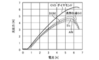
- FIG. 9 shows a result of comparison of current-light output characteristics of the nitride semiconductor light emitting device 100 configured using five types of CVD-diamond, high thermal conductivity SiC, DC60, SiC, and AlN as the submount substrate 111a. It is.
- the AlGaN electron block layer 204 has a composition ratio of Al 0.2 Ga 0.8 N and a thickness of 10 nm, and the optical waveguide Used is an array of five nitride semiconductor lasers.
- Table 4 summarizes the laser characteristics (maximum light output) for each submount substrate material.
- the thermal resistance was obtained by measuring the temperature dependence of the operating voltage when a minute current was applied to one of the five emitters constituting the laser array. It is considered that the difference in thermal resistance due to the difference in the submount 111 reflects the difference in thermal conductivity of the submount 111.
- the difference in maximum light output cannot be explained by the difference in thermal conductivity of the submount 111. For example, when high thermal conductivity SiC and DC60 are compared, DC60 has higher thermal conductivity, but the highest optical output is obtained when the high thermal conductivity SiC submount is used.
- FIG. 10 compares the relationship between the maximum light output and the submount thermal expansion coefficient shown in FIG. 9, which is the experimental result, with the simulation result.
- the points plotted with black circles are actually measured values, and the points plotted with white circles are simulation results.
- the calculation was based on actually measured data when the submount substrate 111a was AlN (thermal conductivity 230 W / mK). Further, it is assumed that the same thermal strain is generated in the nitride semiconductor light emitting device as when mounted using an AlN submount (thermal expansion coefficient 4.5 ⁇ 10 ⁇ 6 / K).
- the submount is CVD-diamond (thermal conductivity 1500 W / mK), DC60 (thermal conductivity 600 W / mK), high thermal conductivity SiC (thermal conductivity 320 W / mK) and normal SiC (thermal conductivity 210 W / mK). mK), the temperature of each element was calculated to determine the maximum light output.
- a material in which the thermal expansion coefficient of the submount is close to that of the nitride semiconductor light emitting element is often selected.
- the difference in thermal expansion coefficient can be positively utilized. That is, when CVD-diamond or SiC having a small thermal expansion coefficient is used, the residual strain (tensile strain) of the AlGaN electron blocking layer 204 is alleviated by compressive thermal strain generated at the time of temperature rise. As a result, the barrier height against electrons in the conduction band is increased.
- the device temperature can be reduced by using a high thermal conductivity SiC submount having a high thermal conductivity, so that a high light output can be obtained.
- DC60 has a very high thermal conductivity of 600 W / mK
- the optical output was lower than that of the high thermal conductivity SiC submount. This indicates that when a submount having a thermal conductivity exceeding 300 W / mK is used, the thermal expansion coefficient has a greater influence on the light output than the thermal conductivity.
- the barrier height of the barrier layer is effectively reduced by relaxing lattice mismatch distortion of the barrier layer (electron block layer) that contributes to carrier confinement in the active layer. Can be expensive.
- an AlGaN electron block is introduced into the light emitting device structure formed on the GaN substrate.
- a lattice mismatch strain in the tensile direction occurs in the electron block layer. Therefore, by mounting the element on a material having a small thermal expansion coefficient, lattice mismatch distortion can be alleviated by thermal distortion generated during energization. As a result, the barrier height of the electron block layer can be effectively increased, and the light output can be increased.
- the thermal expansion coefficient of the submount material is smaller than the thermal expansion coefficient of the nitride semiconductor light emitting device. This is because the lattice mismatch of the electron block layer can be alleviated by thermal strain due to the temperature rise during energization.
- a clearer light output increasing effect can be obtained when the thermal expansion coefficient of the submount is 3 ⁇ 10 ⁇ 6 K ⁇ 1 or less.
- This effect is particularly effective for a light-emitting element that generates a large amount of heat when energized. For example, this is particularly effective for increasing the output of a reactive power that does not contribute to light emission, that is, a device in which the amount of generated heat (Joule heat) exceeds 3 W.
- a material having a high thermal conductivity and a small thermal expansion coefficient such as the above-mentioned CVD-diamond and high thermal conductivity SiC generally has a high manufacturing cost. Therefore, it is difficult to use these materials for products that are expected to be produced at low cost and in large quantities, such as semiconductor lasers.
- the inventors have found that the light output can be increased while suppressing the manufacturing cost by using CVD diamond or high thermal conductivity SiC limited to a part of the submount. That is, it has been found that the nitride semiconductor light emitting device of this embodiment shown in FIGS. 1 to 3 can achieve both a reduction in manufacturing cost and an increase in light output at a high level.
- the surface of the submount 311 close to the nitride semiconductor light emitting element, that is, the first submount substrate 311a has a small thermal expansion coefficient. Use as material. Thereby, compressive thermal strain can be effectively applied to nitride semiconductor light-emitting element 310 when energization is performed.
- the volume of the first submount substrate 311 a needs to be at least larger than the volume of the nitride semiconductor light emitting device 310.
- the nitride semiconductor light emitting device 310 having a length of 800 ⁇ m, a width of 1000 ⁇ m, and a thickness of 80 ⁇ m is used.
- the volume is 0.064 mm2.
- the submount 311 has a length of 1300 ⁇ m, a width of 1400 ⁇ m, and a thickness of 200 ⁇ m.
- the first submount base material 311a made of CVD-diamond has a thickness of 50 ⁇ m.
- the second submount substrate 311b that is, the remaining thickness of 150 ⁇ m is made of AlN.
- the volume of the first submount substrate 311a is 0.091 mm 2 , which is sufficiently larger than the volume of the nitride semiconductor light emitting device 310, and effectively compresses strain in the nitride semiconductor light emitting device 310 due to the temperature rise during energization. Can be given.
- an effect equivalent to that obtained when a single submount made of CVD-diamond is used that is, an improvement in light output as shown in FIG.
- CVD-diamond is used for the first submount substrate 311a, but the present invention is not limited to this. Any material having a thermal expansion coefficient of 4 ⁇ 10 ⁇ 6 K ⁇ 1 or less and a thermal conductivity of 300 W / mK or more can be used.
- the first submount base material 311a the above-described high thermal conductivity SiC can be used, and one having a thermal expansion coefficient adjusted to the above range by increasing the diamond ratio of DC60 can also be used.
- the present invention is not limited to this. Any material having a thermal expansion coefficient smaller than the thermal expansion coefficient of the substrate of the nitride semiconductor light-emitting element and a high thermal conductivity can be used.
- SiC can also be used for the second submount substrate 311b.
- the thermal expansion coefficient of the first submount base material 311a is preferably smaller than the thermal expansion coefficient of the second submount base material 311b.
- the volume of the second submount base material 311b is preferably larger than the volume of the first submount base material 311a in order to reduce the manufacturing cost.
- FIG. 11 is a top view of the nitride semiconductor light emitting device 500 according to the second embodiment as viewed from the light emitting direction.
- the cross-sectional shape and each component are the same as those of the nitride semiconductor light emitting device 100 and the nitride semiconductor light emitting device 300 of the first embodiment shown in FIG. 1, FIG. 2, FIG. 3, and FIG. In FIG. 11, for simplicity of illustration, the cap is not shown.
- the structure of the nitride semiconductor light emitting device 510 is the same as that of the first embodiment.
- FIG. 12 is a schematic diagram in which the structure around the nitride semiconductor light emitting device 510 is enlarged.
- the configuration of the submount 511 is the same as that of the submount 311 shown in FIG.
- the first submount base material 511a connected to the nitride semiconductor light emitting element 510 is made of CVD-diamond
- the second submount base material 511b connected to the element mounting base 522 is made of AlN whose manufacturing cost is low.
- a first electrode 511d and a second electrode made of a metal laminate structure laminated with heat of 0.1 ⁇ m Ti, 0.2 ⁇ m Pt, and 0.2 ⁇ m Au are used.
- An electrode 511f is formed.
- a first bonding portion 511e made of, for example, AuSn eutectic solder is formed, whereby the nitride semiconductor light emitting element 510 and the submount 511 are bonded.
- a second bonding portion 511g made of AuSn eutectic solder is formed, whereby the submount 511 and the element mounting base 522 of the stem 520 are bonded.
- the thicknesses of the first submount base material 511a and the second submount base material 511b are, for example, 10 times or more compared to the thicknesses of the first electrode 511d and the second electrode 511f, respectively.
- the thermal expansion coefficient of the submount 511 it sets so that the thermal expansion coefficient of the two submount base materials 511a and 511b may become dominant.
- the following two points are different from the case of the first embodiment.
- the nitride semiconductor light emitting device 510 has the p-GaN cladding layer 205 side bonded to the submount 511. Further, the submount 511 is bonded to the element mounting base 522 of the stem.
- heat generated from the nitride semiconductor light emitting device 510 is released to the heat sink through the submount 511 and the device mounting base 522.
- heat generation is large in the portion from the MQW active layer to the p-GaN cladding layer. This is because the electrical resistance of the crystal layer in this portion is large, and the ohmic loss due to energization increases. Therefore, when the p-GaN cladding layer 205 side is bonded to the submount 511, the heat dissipation path to the heat sink is shortened, and the thermal resistance is reduced.
- the second difference between the present embodiment and the first embodiment is the shape of the element mounting base 522.
- the lead 523b and the lead 523c are moved rightward (in a direction away from the element mounting base 522) as compared with the structure of FIG. 2, and the sectional area when viewed from the upper surface of the element mounting base 522 is large. . Thereby, the cross-sectional area of the heat dissipation path is enlarged, and the thermal resistance is reduced.
- the temperature rise of the nitride semiconductor light emitting element 510 during energization is suppressed, and a high light output can be obtained.
- the relationship between the thermal expansion coefficient of the submount and the maximum light output is the same as that in the first embodiment. That is, the maximum light output can be increased by using a submount having a small thermal expansion coefficient.
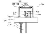
- FIG. 13 is a cross-sectional view of an exemplary nitride semiconductor light emitting device 700 according to the third embodiment, and FIG. 14 is a top view thereof.
- a second submount 712 is added.
- the nitride semiconductor light emitting element 710 is mounted on the element mounting base 722 of the stem 720 together with the submount 711. At this time, the positive electrode side of the nitride semiconductor light emitting device 710 is connected to the submount 711.
- a metal layer is formed on the surface of the submount 711, and the metal layer and the lead 723 b are electrically connected by a bonding wire 740.
- a second submount 712 is bonded to the side facing the submount 711 of the nitride semiconductor light emitting device 710.
- the second submount 712 connects the surface on the negative electrode side of the nitride semiconductor light emitting device 710 and the base 721 of the stem 720.
- a metal layer is also formed on the surface of the second submount 712, and the negative electrode of the nitride semiconductor light emitting device 710 and the base 721 of the stem 720 are electrically connected.
- the ground lead 723a as the negative electrode and the lead 723b as the positive electrode, the nitride semiconductor light emitting device 710 can be energized.
- the negative electrode of the nitride semiconductor light emitting device 710 may be connected to the submount 711 and the positive electrode may be connected to the second submount 712.
- the ground lead 723a is a positive electrode and the lead 723b is a negative electrode.
- the maximum light output can be improved by using a submount having a small thermal expansion coefficient, as in the first embodiment.
- the second submount 712 does not need to be made of the same material as the submount 711, but it is desirable to select a material having a small thermal expansion coefficient (particularly, a smaller thermal expansion coefficient than that of the nitride semiconductor light emitting element). .
- the submount 711 and the second submount 712 need not be made of a single material. That is, similar to the first embodiment, CVD-diamond or high thermal conductivity SiC having a small thermal expansion coefficient may be used on the side connected to the nitride semiconductor light emitting device 710.
- the thermal expansion of the nitride semiconductor light emitting element 710 during energization is largely governed by the thermal expansion coefficient of the second submount 712.
- a material having a small thermal expansion coefficient it is possible to alleviate the lattice mismatch distortion of the electron block layer when the temperature rises and to increase the maximum light output.
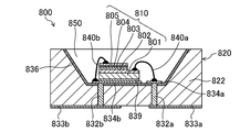
- FIG. 15 is a cross-sectional view of an exemplary nitride semiconductor light emitting device 800 according to the fourth embodiment.
- the nitride semiconductor light emitting device 800 includes a nitride semiconductor light emitting element 810 and a package 820.
- the nitride semiconductor light emitting device 810 includes a GaN substrate 801, an n-cladding layer 802, an MQW active layer 803, a p-AlGaN electron blocking layer 804, and a p-cladding layer 805.
- the nitride semiconductor light emitting device 810 is processed so that a part of the n-cladding layer 802 is exposed by dry etching.
- the package 820 includes an insulating base 822, a reflective film 836 that reflects light from the nitride semiconductor light emitting element 810 in the upper surface direction, back electrodes 833a and 833b, front electrodes 834a and 834b, back electrodes and front electrodes, Via wirings 832a and 832b are connected to each other.
- the nitride semiconductor light emitting device 810 is mounted on the package 820 through an adhesive portion 839.
- a p-electrode (not shown) of nitride semiconductor light emitting device 810 is electrically connected to surface electrode 834b through bonding wire 840b.
- N-electrode (not shown) of nitride semiconductor light emitting device 810 is electrically connected to surface electrode 834a through bonding wire 840a.
- the nitride semiconductor light emitting device 810 can emit light by connecting the backside electrodes 833a and 833b to the negative electrode and the positive electrode, respectively, and applying current.
- the nitride semiconductor light-emitting device 800 is completed by finally embedding the nitride semiconductor light-emitting element 810 with the phosphor-containing resin 850.
- a nitride semiconductor light emitting device 800 that generates white light is provided.
- heat generated in the nitride semiconductor light emitting device 810 is transmitted to the outside through the package base 822. Therefore, it is desirable to use a material with high thermal conductivity for the base material 822. Further, the thermal strain generated in the nitride semiconductor light emitting element 810 that is energized is determined by the thermal expansion coefficient of the base material 822. Therefore, similar to the submount of the first embodiment, CVD-diamond or high thermal conductivity SiC having a low thermal expansion coefficient and high thermal conductivity is formed on the side of the base material 822 connected to the nitride semiconductor light emitting device 810. Use. Thereby, the carrier overflow suppression effect of the electron block layer 804 is increased. As a result, high light output can be obtained.
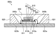
- FIG. 16 is a cross-sectional view showing a modification of the fourth embodiment.
- the nitride semiconductor light emitting device 800a includes a nitride semiconductor light emitting element 810, a package 820, and a submount 811.
- the nitride semiconductor light emitting device 810 is the same as that of FIG.
- the package 820 includes a resin base 821 and metal leads 823a and 823b electrically separated by the resin base 821.
- the nitride semiconductor light emitting device 810 is connected to the submount 811 and is mounted on the package 820 together with the submount 811.
- Surface electrodes 812 a and 812 b are formed on the surface of the submount 811.
- the p-electrode of the nitride semiconductor light emitting device 810 is connected to the surface electrode 812b, and the n-electrode is connected to the surface electrode 812a via the bump electrode 815.
- the surface electrodes 812a and 812b are electrically connected to the metal leads 823a and 823b by bonding wires 840a and 840b, respectively.
- the nitride semiconductor light emitting device 810 can emit light by connecting the metal leads 823a and 823b to the negative electrode and the positive electrode, respectively, and energizing them.
- the nitride semiconductor light emitting device 800 is completed by embedding the nitride semiconductor light emitting element 810 with the phosphor-containing resin 850. When the nitride semiconductor light emitting element 810 that emits blue light and the phosphor-containing resin 850 that emits yellow fluorescence are used, a nitride semiconductor light emitting device 800 that generates white light is provided.
- heat generated in the nitride semiconductor light emitting device 810 is transmitted to the outside through the submount 811 and the metal lead 823b. Therefore, it is desirable to use a material having high thermal conductivity for the submount 811. Further, the thermal strain generated in the nitride semiconductor light emitting element 810 that is energized is determined by the thermal expansion coefficient of the submount 811. Therefore, similar to the submount of the first embodiment, CVD-diamond or high thermal conductivity SiC having a small thermal expansion coefficient and high thermal conductivity is formed on the side of the submount 811 that is connected to the nitride semiconductor light emitting element 810. Use. Thereby, the carrier overflow suppression effect of the electron block layer 804 is increased. As a result, high light output can be obtained.
- CVD-diamond or SiC is used as the material of the package substrate 822.
- these materials can be used for the submount 811 in this modification. Since the submount is a simple rectangular parallelepiped, there is an advantage that it can be easily processed.
- the light output can be improved by mounting the nitride semiconductor light emitting element using the electron block layer having the lattice mismatch strain in the tensile direction on the submount having a small thermal expansion coefficient.
- the shape of the submount may be a simple rectangular parallelepiped and does not require complicated mechanical processing. Therefore, a material with low workability such as the artificial diamond described in this embodiment can be used. Further, since a conventional stem or cap can be used as it is, it can be easily mounted on a conventional light source using a nitride semiconductor light emitting device.
- the nitride semiconductor light emitting device of the present invention is effective for devices that require a relatively high light output such as image display devices such as laser displays and projectors, and industrial laser equipment such as laser processing and laser annealing.
- the nitride semiconductor light emitting element used in this nitride semiconductor light emitting device is widely applicable not only to semiconductor lasers but also to elements such as light emitting diodes.
- SYMBOLS 100 Nitride semiconductor light-emitting device 100a Nitride semiconductor light-emitting device 110 Nitride semiconductor light-emitting device 111 Submount 111a Submount 111d Electrode 111e Adhesion part 111f Electrode 111g Adhesion part 120 Stem 121 Base 122 Element mounting base 123a Earth lead 123b Lead 123c Lead 130 Cap 131 Cover 131a Opening 132 Window 140b Bonding wire 140c Bonding wire 201 Nitride semiconductor substrate 202 Clad layer 203 Active layer 204 Electron block layer 205 Clad layer 206 Contact layer 210 p-ohmic electrode 211 n-ohmic electrode 221 strain 221a strain 222 Compressive strain 300 Nitride semiconductor light emitting device DESCRIPTION OF SYMBOLS 10 Nitride semiconductor light emitting element 311 Submount 311a 1st submount base material 311b 2nd submount base material 311d Electrode 311e Bonding part 311f Electrode 311g
Abstract
A semiconductor light emitting device (300) has: a nitride semiconductor light emitting element (310), which has a nitride semiconductor multilayer film laminated on a nitride semiconductor substrate (201) that has a polar surface or a semipolar surface as the surface; and a mounting section (311) having the element mounted thereon. The nitride semiconductor multilayer film includes an electron block layer (204). The electron block layer has a lattice constant smaller than that of the nitride semiconductor substrate. The mounting section has at least a first mounting section base material (311a). The first mounting section base material is positioned on the side where the nitride semiconductor light emitting element is to be mounted. The first mounting section base material has a thermal expansion coefficient smaller than that of the nitride semiconductor multilayer film. The first mounting section base material has thermal conductivity higher than that of the nitride semiconductor multilayer film.
Description
本開示は、発光装置、特に、プロジェクタ、液晶バックライト等の光源に用いられる光出力の大きな窒化物半導体発光装置の構造に関する。
The present disclosure relates to a structure of a light emitting device, in particular, a nitride semiconductor light emitting device having a large light output used for a light source such as a projector or a liquid crystal backlight.
近年、機器の省エネ化に伴い、窒化物半導体を用いた発光ダイオードや半導体レーザ等の窒化物半導体発光素子を実装した窒化物半導体発光装置が注目されている。例えば、窒化物半導体発光装置と蛍光体等を組み合わせた光源は、高光出力の白色光を出射させることができると共に、従来の白熱電球や蛍光灯、高圧水銀ランプに比べて、小型、高効率、長寿命といった特徴を有するので、プロジェクタ、液晶バックライト等のディスプレイ装置用途の光源として、急速に置き換えが進んでいる。
In recent years, with the energy saving of devices, a nitride semiconductor light emitting device in which a nitride semiconductor light emitting element such as a light emitting diode using a nitride semiconductor or a semiconductor laser is mounted has attracted attention. For example, a light source combining a nitride semiconductor light-emitting device and a phosphor can emit white light with high light output, and is smaller and more efficient than conventional incandescent bulbs, fluorescent lamps, and high-pressure mercury lamps. Since it has a feature such as long life, it is rapidly being replaced as a light source for display devices such as projectors and liquid crystal backlights.
一方、窒化物半導体レーザに代表される、導波路を有する窒化物半導体発光素子は、光を放射する方向を示す指向性に優れているという特徴がある。そこで、このような窒化物半導体発光素子を実装した窒化物半導体発光装置の産業用途への応用も進んでいる。例えば、窒化物半導体発光装置を光源としたレーザスクライブ装置やレーザアニール装置については、実用化の検討が進んでいる。これらの装置に用いる光源には、光出力が1ワット以上のワットクラスの高い光出力が必要とされるので、窒化物半導体発光装置にも高出力化が要望されている。
On the other hand, a nitride semiconductor light emitting device having a waveguide, represented by a nitride semiconductor laser, is characterized by excellent directivity indicating the direction of light emission. Then, the application to the industrial use of the nitride semiconductor light-emitting device which mounted such a nitride semiconductor light-emitting element is also advancing. For example, practical application of a laser scribing apparatus and a laser annealing apparatus using a nitride semiconductor light emitting device as a light source is proceeding. Since the light source used in these devices requires a high light output in the watt class with an optical output of 1 watt or more, the nitride semiconductor light emitting device is also required to have a high output.
窒化物半導体発光素子等の発光素子は、量子井戸等により構成される活性層に、電子と正孔(電子正孔対)を注入し、再結合させることによって光を放射する。このとき、光に変換されなかったエネルギーはジュール熱となり、素子の温度を上昇させる。窒化物半導体発光装置を高出力化するためには、注入する電流(電子、正孔)量を大きくする必要があるが、電流の増加は窒化物半導体発光素子の発熱を増大させる。そして、この発熱によって素子温度が上昇すると、電子又は正孔の一部が活性層に注入されず、あふれ出る現象(キャリアのオーバーフローと呼ばれる現象)が発生する。この場合、電流量を増加させても光出力が増加しなくなり、最終的には光出力が飽和する現象(光飽和)が発生する。従って、高い光出力を得るためには、チップ温度の上昇を抑制する共に、キャリアのオーバーフローを抑制し、効率良く電子正孔対を光に変換させる必要がある。
A light-emitting device such as a nitride semiconductor light-emitting device emits light by injecting electrons and holes (electron-hole pairs) into an active layer composed of quantum wells and recombining them. At this time, the energy that has not been converted to light becomes Joule heat, which raises the temperature of the element. In order to increase the output of the nitride semiconductor light emitting device, it is necessary to increase the amount of current (electrons and holes) to be injected. However, the increase in current increases the heat generation of the nitride semiconductor light emitting element. When the element temperature rises due to this heat generation, a part of electrons or holes is not injected into the active layer and an overflow phenomenon (a phenomenon called carrier overflow) occurs. In this case, even if the amount of current is increased, the light output does not increase, and eventually a phenomenon (light saturation) in which the light output is saturated occurs. Therefore, in order to obtain a high light output, it is necessary to suppress an increase in the chip temperature, suppress a carrier overflow, and efficiently convert an electron-hole pair into light.
そこで、このようなキャリアのオーバーフローを抑制する方法として、従来技術では、エネルギーバンドギャップの大きな層を活性層近傍に挿入する手法が用いられる。特許文献1には従来の窒化物半導体レーザの構造が示されている。図17(a)はその構造を示す図である。図17(b)はそのエネルギーバンドギャップの伝導帯側を示している。
Therefore, as a method of suppressing such carrier overflow, a method of inserting a layer having a large energy band gap in the vicinity of the active layer is used in the conventional technique. Patent Document 1 shows a structure of a conventional nitride semiconductor laser. FIG. 17A shows the structure. FIG. 17B shows the conduction band side of the energy band gap.
図17(a)に示したように、従来構造の窒化物半導体レーザでは、GaN基板1001及びn-GaN層1002上に、n-AlGaNクラッド層1003、InGaN活性層1005、p-AlGaN電子オーバーフロー抑制層1010(この層は本明細書中では電子ブロック層と呼ぶ)、p-AlGaNクラッド層1011、p-GaNコンタクト層1012を含む積層構造を有している。
As shown in FIG. 17A, in the nitride semiconductor laser having the conventional structure, the n-AlGaN cladding layer 1003, the InGaN active layer 1005, and the p-AlGaN electron overflow are suppressed on the GaN substrate 1001 and the n-GaN layer 1002. It has a stacked structure including a layer 1010 (this layer is called an electron blocking layer in this specification), a p-AlGaN cladding layer 1011, and a p-GaN contact layer 1012.
電子ブロック層1010は、n-GaN層1002から注入された電子が活性層1005を通過してp-AlGaNクラッド層1011へあふれて出ていくことを防ぐために設けられた層である。図17(b)に示したように、電子ブロック層1010は周辺の層よりも大きなエネルギーバンドギャップを有している。電子ブロック層1010には、エネルギーバンドギャップを大きくするために、Al組成の大きなAlGaN層が用いられている。
The electron block layer 1010 is a layer provided to prevent electrons injected from the n-GaN layer 1002 from passing through the active layer 1005 and overflowing to the p-AlGaN cladding layer 1011. As shown in FIG. 17B, the electron block layer 1010 has a larger energy band gap than the surrounding layers. For the electron block layer 1010, an AlGaN layer having a large Al composition is used in order to increase the energy band gap.
一方、窒化物半導体において、格子不整合歪みによってピエゾ電界が発生する場合がある。上述したp-AlGaN電子ブロック層1010の格子定数は、GaN基板1001の格子定数よりも小さな値をもつ。この点から、p-AlGaN電子ブロック層1010には引っ張り歪みが発生し、その歪みによってピエゾ電解が発生する。p-AlGaN電子ブロック層による電子閉じ込め効果は、このピエゾ電界によって低下する。
On the other hand, in a nitride semiconductor, a piezoelectric field may be generated due to lattice mismatch distortion. The lattice constant of the p-AlGaN electron block layer 1010 described above has a smaller value than the lattice constant of the GaN substrate 1001. From this point, tensile strain is generated in the p-AlGaN electron block layer 1010, and piezoelectrolysis is generated by the strain. The electron confinement effect by the p-AlGaN electron block layer is reduced by this piezo electric field.
特許文献2には、ピエゾ電界によって電子に対する実効的な障壁高さが減少することが示されている。そこで、特許文献2では、電子を閉じ込めるp-AlGaNブロック層を厚くする方法を提案している。AlGaN層の厚さが厚くなると、転位やクラックの発生によって、弾性的な格子不整合歪みは緩和される。これにより、格子不整合歪みに起因したピエゾ電界は減少し、結果として伝導帯の電子に対する障壁高さが増大する。
Patent Document 2 shows that the effective barrier height against electrons is reduced by the piezoelectric field. Therefore, Patent Document 2 proposes a method of increasing the thickness of the p-AlGaN block layer that confines electrons. When the thickness of the AlGaN layer is increased, elastic lattice mismatch strain is relaxed due to the generation of dislocations and cracks. This reduces the piezo electric field due to lattice mismatch distortion, resulting in an increase in barrier height for electrons in the conduction band.
しかし、転位やクラック等塑性変形は、素子の特性や信頼性に大きく影響する。特にGaN基板上のAlGaN層は引っ張り歪みを有していることからクラックが生じやすい。クラック周辺では、ウェハ表面は平坦でなくなるので、正常な素子を作製すること自体が極めて困難となる。
However, plastic deformation such as dislocations and cracks greatly affects the characteristics and reliability of the device. In particular, since the AlGaN layer on the GaN substrate has tensile strain, cracks are likely to occur. Since the wafer surface is not flat around the crack, it is extremely difficult to manufacture a normal device.
上述のように、窒化物半導体を用いた発光素子において、格子不整合歪みに起因したピエゾ電界の影響によって、キャリアのオーバーフローを抑制する効果が低下する。この現象は、(0001)面を代表とする極性面を窒化物半導体発光素子構造の主面とした場合に共通して起こる現象である。伝導帯の電子に対する実効的な障壁高さを高くするためには、電子を閉じ込める作用をもつAlGaN層のAl組成を高くする必要がある。しかし、Al組成を高くすると格子不整合歪が増大し、転位やクラックが発生しやすくなるという特許文献2に示された手法と同じ問題を抱えている。
As described above, in a light emitting device using a nitride semiconductor, the effect of suppressing carrier overflow is reduced by the influence of a piezoelectric field caused by lattice mismatch distortion. This phenomenon occurs in common when a polar surface typified by the (0001) plane is used as the main surface of the nitride semiconductor light emitting device structure. In order to increase the effective barrier height for electrons in the conduction band, it is necessary to increase the Al composition of the AlGaN layer that has the effect of confining electrons. However, when the Al composition is increased, the lattice mismatch strain increases, and the same problem as the method disclosed in Patent Document 2 that dislocations and cracks are likely to occur occurs.
本発明の目的は、塑性変形をともなわずにピエゾ電界の影響を低減し、効果的に窒化物半導体発光素子におけるキャリアのオーバーフローを低減できる窒化物半導体発光装置を提供することにある。すなわち、より高出力での動作が可能な窒化物半導体発光装置の構成を提供することができる。
An object of the present invention is to provide a nitride semiconductor light emitting device capable of reducing the influence of a piezoelectric field without plastic deformation and effectively reducing the overflow of carriers in the nitride semiconductor light emitting element. That is, it is possible to provide a configuration of a nitride semiconductor light emitting device that can operate at a higher output.
そこで、本願発明者らは、窒化物半導体発光素子中の電子ブロック層に形成されるピエゾ電界と、窒化物半導体発光素子を実装した窒化物半導体発光装置の構成との関係に着目した。具体的には、窒化物半導体発光素子を搭載するサブマウントの熱膨張率を制御することによって、素子の温度が上昇した場合においてもキャリアのオーバーフローを効果的に抑制できることを見出した。その結果、光出力を増加させる窒化物半導体発光装置の構成を見出した。
Therefore, the inventors of the present application paid attention to the relationship between the piezoelectric field formed in the electron block layer in the nitride semiconductor light emitting element and the configuration of the nitride semiconductor light emitting device mounted with the nitride semiconductor light emitting element. Specifically, it has been found that by controlling the coefficient of thermal expansion of the submount on which the nitride semiconductor light emitting element is mounted, carrier overflow can be effectively suppressed even when the temperature of the element rises. As a result, the inventors have found a nitride semiconductor light emitting device configuration that increases the light output.
具体的に、本開示の窒化物半導体発光装置は、表面に極性面又は半極性面を有する窒化物半導体基板上に、窒化物半導体多層膜が積層された構成を有する窒化物半導体発光素子と、窒化物半導体発光素子を搭載する搭載部とを有する半導体発光装置において、窒化物半導体多層膜は、電子ブロック層を含み、電子ブロック層の格子定数は、窒化物半導体基板の格子定数よりも小さく、搭載部は、少なくとも第1の搭載部基材を有し、第1の搭載部基材は、窒化物半導体発光素子が搭載される側に位置しており、第1の搭載部基材の熱膨張係数は、窒化物半導体多層膜の熱膨張係数よりも小さく、第1の搭載部基材の熱伝導率は、窒化物半導体多層膜の熱伝導率よりも大きい。
Specifically, the nitride semiconductor light emitting device of the present disclosure includes a nitride semiconductor light emitting element having a configuration in which a nitride semiconductor multilayer film is stacked on a nitride semiconductor substrate having a polar surface or a semipolar surface on the surface; In a semiconductor light emitting device having a mounting portion on which a nitride semiconductor light emitting element is mounted, the nitride semiconductor multilayer film includes an electron block layer, and the lattice constant of the electron block layer is smaller than the lattice constant of the nitride semiconductor substrate, The mounting portion has at least a first mounting portion base material, and the first mounting portion base material is located on the side on which the nitride semiconductor light emitting element is mounted, and the heat of the first mounting portion base material is The expansion coefficient is smaller than the thermal expansion coefficient of the nitride semiconductor multilayer film, and the thermal conductivity of the first mounting portion base material is larger than the thermal conductivity of the nitride semiconductor multilayer film.
この構成により、通電により素子の温度が上昇した場合においてもキャリアのオーバーフローを効果的に抑制でき、光出力を増加させることができる窒化物半導体発光装置を、低コストで実現できる。ここで、搭載部は、第1の搭載部基材のみによって構成されていても良い。
With this configuration, a nitride semiconductor light emitting device capable of effectively suppressing carrier overflow and increasing light output even when the temperature of the element increases due to energization can be realized at low cost. Here, the mounting portion may be configured only by the first mounting portion base material.
尚、第1の搭載部基材の熱膨張係数は、4×10⁻⁶K-1以下であり、第1の搭載部基材の熱伝導率は、300W/mK以上であっても良い。
The first mounting portion base material may have a thermal expansion coefficient of 4 × 10 −6 K −1 or lower, and the first mounting portion base material may have a thermal conductivity of 300 W / mK or higher.
このようにすると、より確実に素子の温度が上昇した場合においてもキャリアのオーバーフローを効果的に抑制でき、光出力を増加させることができる。
In this way, even when the temperature of the element rises more reliably, carrier overflow can be effectively suppressed and the light output can be increased.
また、搭載部は、第1の搭載部基材とは異なる材料からなり、且つ、第1の搭載部基材と接合される第2の搭載部基材を備え、第1の搭載部基材は、第2の搭載部基材よりも窒化物半導体発光素子に近い側に位置していても良い。
The mounting portion includes a second mounting portion base material made of a material different from that of the first mounting portion base material and joined to the first mounting portion base material. May be located closer to the nitride semiconductor light emitting element than the second mounting portion base material.
このようにすると、第1の搭載部基材が高コストな材料からなる場合に、その使用量を削減しながら前記の効果を実現することができる。
In this way, when the first mounting portion base material is made of a high-cost material, the above-described effects can be realized while reducing the amount of use.
また、第1の搭載部基材は、高熱伝導SiCセラミック、CVD-ダイヤモンド、又は、ダイヤモンドと銅との複合材の何れかからなっていても良い。
Further, the first mounting portion base material may be made of any one of high thermal conductivity SiC ceramic, CVD-diamond, or a composite material of diamond and copper.
この構成により、窒化物半導体発光素子からヒートシンクまでの熱抵抗を効果的に低減して、温度上昇にともなう光出力の低下を抑制することができる。
With this configuration, it is possible to effectively reduce the thermal resistance from the nitride semiconductor light emitting element to the heat sink, and to suppress a decrease in light output accompanying a temperature rise.
また、第1の搭載部基材の熱膨張係数が3×10⁻⁶K-1以下であっても良い。
Further, the first mounting portion base material may have a thermal expansion coefficient of 3 × 10 −6 K −1 or less.
この構成により、窒化物半導体発光素子に十分な圧縮歪みを生じさせ、効果的に光出力の増大を実現できる。
With this configuration, sufficient compressive strain is generated in the nitride semiconductor light emitting device, and an increase in light output can be effectively realized.
また、窒化物半導体発光素子のジュール熱が3W以上であってもよい。
Further, the Joule heat of the nitride semiconductor light emitting element may be 3 W or more.
本開示の窒化物半導体発光装置は、このような光出力が高く発熱量が多い場合において特に効果が大きい。
The nitride semiconductor light emitting device of the present disclosure is particularly effective when the light output is high and the heat generation amount is large.
また、窒化物半導体発光素子が半導体レーザ素子であってもよい。
The nitride semiconductor light emitting element may be a semiconductor laser element.
半導体レーザ素子では、注入キャリアの活性層への閉じ込めが発光特性に大きく影響する。そのため、この構成により半導体レーザの高出力特性を大きく改善することができる。
In semiconductor laser elements, the confinement of injected carriers in the active layer greatly affects the light emission characteristics. Therefore, this configuration can greatly improve the high output characteristics of the semiconductor laser.
また、窒化物半導体発光素子が発光ダイオードであってもよい。
The nitride semiconductor light emitting element may be a light emitting diode.
この構成により温度上昇をともなう大電流駆動時に効果的に高い光出力を得ることができる。
This configuration makes it possible to obtain a high light output effectively when driving a large current with a temperature rise.
また、第1の搭載部基材の熱膨張係数は、第2の搭載部基材の熱膨張係数よりも小さくても良い。
Further, the thermal expansion coefficient of the first mounting portion base material may be smaller than the thermal expansion coefficient of the second mounting portion base material.
この構成により、窒化物半導体発光素子に十分な圧縮歪みを生じさせ、効果的に光出力の増大を実現できる。
With this configuration, sufficient compressive strain is generated in the nitride semiconductor light emitting device, and an increase in light output can be effectively realized.
また、第1の搭載部基材の体積は、前記窒化物半導体発光素子の体積より大きいことが好ましい。
The volume of the first mounting portion base material is preferably larger than the volume of the nitride semiconductor light emitting device.
この構成により、窒化物半導体発光素子に十分な圧縮歪みを生じさせ、効果的に光出力の増大を実現できる。また、製造コストを大幅に削減することができる。
With this configuration, sufficient compressive strain is generated in the nitride semiconductor light emitting device, and an increase in light output can be effectively realized. In addition, the manufacturing cost can be greatly reduced.
また、搭載部は、更に他の素子搭載台又は基材に搭載されるサブマウントであってもよい。
Further, the mounting portion may be a submount mounted on another element mounting base or base material.
このようにすると、例えば直方体等の形成が容易なサブマウントに窒化物半導体発光素子を搭載し、これを更に他の素子搭載台、基材、ステム等に対して搭載する構成とすることができる。従って、搭載部の材料の加工性が低い場合等にも対応できる。
In this way, for example, a nitride semiconductor light emitting element can be mounted on a submount that can be easily formed into a rectangular parallelepiped, and this can be mounted on another element mounting base, base material, stem, or the like. . Therefore, it is possible to cope with the case where the workability of the material of the mounting portion is low.
本発明の構成によれば、通電により素子の温度が上昇した場合においてもキャリアのオ
ーバーフローを効果的に抑制でき、光出力を増加させることができる窒化物半導体発光装置を、低コストで実現できる。 According to the configuration of the present invention, it is possible to realize a nitride semiconductor light emitting device that can effectively suppress the overflow of carriers and increase the light output even when the temperature of the element rises due to energization at low cost.
ーバーフローを効果的に抑制でき、光出力を増加させることができる窒化物半導体発光装置を、低コストで実現できる。 According to the configuration of the present invention, it is possible to realize a nitride semiconductor light emitting device that can effectively suppress the overflow of carriers and increase the light output even when the temperature of the element rises due to energization at low cost.
以下、図面を参照して本開示の実施の形態について説明する。
Hereinafter, embodiments of the present disclosure will be described with reference to the drawings.
(第1の実施形態)
図1及び図2に、本実施形態の例示的窒化物半導体発光装置300の構成を図示する。図1は窒化物半導体発光装置の断面図、図2は窒化物半導体発光装置の光出射方向(図1における上側)から見た上面図をそれぞれ示している。 (First embodiment)
FIG. 1 and FIG. 2 illustrate the configuration of an exemplary nitride semiconductorlight emitting device 300 of this embodiment. FIG. 1 is a cross-sectional view of a nitride semiconductor light emitting device, and FIG. 2 is a top view of the nitride semiconductor light emitting device viewed from the light emitting direction (upper side in FIG. 1).
図1及び図2に、本実施形態の例示的窒化物半導体発光装置300の構成を図示する。図1は窒化物半導体発光装置の断面図、図2は窒化物半導体発光装置の光出射方向(図1における上側)から見た上面図をそれぞれ示している。 (First embodiment)
FIG. 1 and FIG. 2 illustrate the configuration of an exemplary nitride semiconductor
本実施形態の窒化物半導体発光装置300は、例えば主波長が390nmから550nmのいずれかであるレーザ光を放射する窒化物半導体発光素子310、窒化物半導体発光素子310を搭載するサブマウント311、ステム120及びキャップ130から構成される。
The nitride semiconductor light emitting device 300 of this embodiment includes, for example, a nitride semiconductor light emitting element 310 that emits laser light having a dominant wavelength of 390 nm to 550 nm, a submount 311 on which the nitride semiconductor light emitting element 310 is mounted, and a stem. 120 and a cap 130.
ステム120は、基台121及び素子搭載台122と、アースリード123a、リード123b及び123cとからなる。窒化物半導体発光素子310及びサブマウント311は、素子搭載台122に接着される。窒化物半導体発光素子310は、ボンディングワイヤ140b及び140cによってリード123b及び123cに電気的に接続される。本実施形態において、正電極は窒化物半導体発光素子310の上面のp電極からリード123bにボンディングワイヤ140bによって接続されている。負電極は、サブマウント311の表面に形成された第一の電極からリード123cにボンディングワイヤ140cによって接続されている。キャップ130は、開口部131aを有するカバー131と光取り出し窓132とによって構成される。キャップ130はステムの基台121に溶接される。この構成により、窒化物半導体発光素子310は気密封止される。
The stem 120 includes a base 121 and an element mounting base 122, and ground leads 123a, leads 123b and 123c. The nitride semiconductor light emitting device 310 and the submount 311 are bonded to the device mounting base 122. The nitride semiconductor light emitting device 310 is electrically connected to the leads 123b and 123c by bonding wires 140b and 140c. In the present embodiment, the positive electrode is connected to the lead 123b from the p electrode on the upper surface of the nitride semiconductor light emitting device 310 by the bonding wire 140b. The negative electrode is connected to the lead 123c from the first electrode formed on the surface of the submount 311 by a bonding wire 140c. The cap 130 includes a cover 131 having an opening 131a and a light extraction window 132. The cap 130 is welded to the stem base 121. With this configuration, the nitride semiconductor light emitting device 310 is hermetically sealed.
続いて、図3を用いて窒化物半導体発光装置300の構成を詳細に説明する。図3は窒化物半導体発光素子310およびサブマウント311の詳細な積層構造である。以下、まず、窒化物半導体発光素子310の代表的な構造と製造方法について説明する。
Subsequently, the configuration of the nitride semiconductor light emitting device 300 will be described in detail with reference to FIG. FIG. 3 shows a detailed stacked structure of the nitride semiconductor light emitting device 310 and the submount 311. Hereinafter, first, a typical structure and manufacturing method of the nitride semiconductor light emitting device 310 will be described.
窒化物半導体発光素子310はn-GaN(0001)基板である窒化物半導体基板201上に、有機金属気相成長法(Matalorganic Chemical Vapor Deposition; MOCVD)によって形成された窒化物半導体多層膜によって構成される。より具体的には、窒化物半導体基板201上に、n-AlGaNであるクラッド層202、n-GaNからなるガイド層/InGaN多重量子井戸/p-GaNからなるガイド層の3種類の層を含む活性層203、Al組成比が例えば15~30%と高いAlGaN電子ブロック層204、p-AlGaNからなるクラッド層205、及びp-GaNからなるコンタクト層206が順次積層されている。ここで、窒化物半導体基板201の表面の面方位は(0001)に限られず、極性もしくは半極性面を含んでいれば良い。また、AlGaN電子ブロック層204の組成は上述した組成に限られず、窒化物半導体発光素子の基板よりも格子定数が小さければ良い。
The nitride semiconductor light emitting device 310 is constituted by a nitride semiconductor multilayer film formed on a nitride semiconductor substrate 201, which is an n-GaN (0001) substrate, by metal organic chemical vapor deposition (MOCVD). The More specifically, the nitride semiconductor substrate 201 includes three types of layers: a clad layer 202 made of n-AlGaN, a guide layer made of n-GaN / InGaN multiple quantum wells / a guide layer made of p-GaN. An active layer 203, an AlGaN electron blocking layer 204 having an Al composition ratio as high as 15 to 30%, a clad layer 205 made of p-AlGaN, and a contact layer 206 made of p-GaN are sequentially stacked. Here, the plane orientation of the surface of the nitride semiconductor substrate 201 is not limited to (0001), but may include a polar or semipolar plane. Further, the composition of the AlGaN electron blocking layer 204 is not limited to the above-described composition, and it is sufficient that the lattice constant is smaller than that of the substrate of the nitride semiconductor light emitting device.
この積層構造の表面には、一つ又は複数のリッジ型導波路(図示なし)がドライエッチングプロセスを用いて形成されている。更に、コンタクト層206表面には、例えばPd/Pt/Auからなるp-オーミック電極210が形成され、窒化物半導体基板201の裏面には、例えばTi/Pt/Auからなるn-オーミック電極211が形成されている。尚、リッジ型導波路が例えば長さ800μmに劈開されることにより、ファブリーペロー型共振器が形成され、レーザ構造として機能する。
On the surface of this laminated structure, one or a plurality of ridge-type waveguides (not shown) are formed using a dry etching process. Further, a p-ohmic electrode 210 made of, for example, Pd / Pt / Au is formed on the surface of the contact layer 206, and an n-ohmic electrode 211 made of, for example, Ti / Pt / Au is formed on the back surface of the nitride semiconductor substrate 201. Is formed. Note that, when the ridge-type waveguide is cleaved to a length of, for example, 800 μm, a Fabry-Perot resonator is formed and functions as a laser structure.
続いて、サブマウント311について説明する。サブマウント311は、第1のサブマウント基材311aと第2のサブマウント基材311bとを備える。第2のサブマウント基材311bには、例えば、比較的低コストにて作製可能なAlNセラミックを使用することができる。そして、第2のサブマウント基材311bの表面にCVD法によってダイヤモンドを堆積して第1のサブマウント基材311aを形成し、二層構造のサブマウント311を構成することができる。このような複合材をサブマウントに用いることにより、サブマウントの熱伝導率を高め、且つ、熱膨張係数を小さく設定することができる。
Subsequently, the submount 311 will be described. The submount 311 includes a first submount base material 311a and a second submount base material 311b. For the second submount substrate 311b, for example, an AlN ceramic that can be manufactured at a relatively low cost can be used. Then, diamond can be deposited on the surface of the second submount base material 311b by a CVD method to form the first submount base material 311a, and the submount 311 having a two-layer structure can be configured. By using such a composite material for the submount, the thermal conductivity of the submount can be increased and the thermal expansion coefficient can be set small.
サブマウント311の表面及び裏面には、例えば、Tiを0.1μm、Ptを0.2μm、Auを0.2μmの層として積層した金属積層構造からなる第一の電極311d及び第二の電極311fが形成されている。
On the front and back surfaces of the submount 311, for example, a first electrode 311 d and a second electrode 311 f having a metal laminated structure in which Ti is laminated as a layer of 0.1 μm, Pt is 0.2 μm, and Au is 0.2 μm. Is formed.
更に、第一の電極311d上には、例えばAuSn共晶はんだである第一の接着部311eが形成されて、これによりサブマウント311と窒化物半導体発光素子310との接着が行われている。サブマウント311の第二の電極311f上には、例えばAuSn共晶はんだである第二の接着部311gが形成されて、これによりサブマウント311とステム120の素子搭載台122との接着が行われている。
Furthermore, on the first electrode 311d, a first bonding portion 311e made of, for example, AuSn eutectic solder is formed, whereby the submount 311 and the nitride semiconductor light emitting element 310 are bonded. On the second electrode 311 f of the submount 311, for example, a second bonding portion 311 g made of AuSn eutectic solder is formed, and thereby the submount 311 and the element mounting base 122 of the stem 120 are bonded to each other. ing.
上記の構成において、第1のサブマウント基材311a及び第2のサブマウント基材311bの厚みが、それぞれ、第一の電極311d及び第二の電極311fの厚みに比べて例えば10倍以上になるように設定する。これにより、サブマウント311の熱膨張係数に関して、二つのサブマウント基材311a、311bの熱膨張係数が支配的になるように設定される。 以上が本実施形態の窒化物半導体発光装置の構成である。本実施形態の窒化物半導体発光装置を動作させたところ、通電により素子の温度が上昇した場合においてもキャリアのオーバーフローを効果的に抑制できた。その結果、光出力を増加させることに成功した。
In the above configuration, the thickness of the first submount base material 311a and the second submount base material 311b is, for example, 10 times or more compared to the thickness of the first electrode 311d and the second electrode 311f, respectively. Set as follows. Thereby, regarding the thermal expansion coefficient of the submount 311, it sets so that the thermal expansion coefficient of the two submount base materials 311a and 311b may become dominant. The above is the configuration of the nitride semiconductor light emitting device of this embodiment. When the nitride semiconductor light emitting device of this embodiment was operated, carrier overflow could be effectively suppressed even when the temperature of the element increased due to energization. As a result, we succeeded in increasing the light output.
次に、図4~図10を用いて、本願発明者らが本実施形態の窒化物半導体発光装置の効果を検証するために行った実験結果を示す。
Next, with reference to FIG. 4 to FIG. 10, the results of experiments conducted by the present inventors to verify the effect of the nitride semiconductor light emitting device of this embodiment will be shown.
図4は、本願発明者らが、本実施形態の効果を検証するために作製した窒化物半導体発光装置100を示す図である。窒化物半導体発光装置100の形状及び構成部品は、図1及び図2に示した窒化物半導体発光装置300と同一であり、図4において、キャップ130を省略し、光出射方向からみた上面図として示されている。
FIG. 4 is a diagram showing a nitride semiconductor light emitting device 100 manufactured by the present inventors in order to verify the effect of the present embodiment. The shape and components of the nitride semiconductor light emitting device 100 are the same as those of the nitride semiconductor light emitting device 300 shown in FIGS. 1 and 2, and in FIG. 4, the cap 130 is omitted and a top view as seen from the light emitting direction. It is shown.
図5(a)及び図5(b)は、窒化物半導体発光装置100の窒化物半導体発光素子110付近の詳細な構造と、そのエネルギーバンドギャップの構成(以下バンドラインアップと呼ぶ)を示す図である。窒化物半導体発光素子110の構造は、サブマウント111が、単一のサブマウント基材111aだけを有する点を除いて、図3の窒化物半導体発光素子310と同一である。
FIGS. 5A and 5B are diagrams showing a detailed structure in the vicinity of the nitride semiconductor light emitting element 110 of the nitride semiconductor light emitting device 100 and a configuration of the energy band gap (hereinafter referred to as band line up). It is. The structure of the nitride semiconductor light emitting device 110 is the same as that of the nitride semiconductor light emitting device 310 of FIG. 3 except that the submount 111 has only a single submount substrate 111a.
図6(a)及び図6(b)は、窒化物半導体発光装置100aの機能を説明するための図である。窒化物半導体発光装置100aは、サブマウント基材111aの材料以外は、図5(a)及び(b)の窒化物半導体発光装置100と同様である。
FIG. 6A and FIG. 6B are diagrams for explaining the function of the nitride semiconductor light emitting device 100a. The nitride semiconductor light emitting device 100a is the same as the nitride semiconductor light emitting device 100 of FIGS. 5A and 5B except for the material of the submount substrate 111a.
表1は、後述するサブマウント材料に適用可能な材料の特性一覧である。
Table 1 is a list of characteristics of materials applicable to the submount materials described later.
図7は、表1に示した材料の特性を示す図である。
FIG. 7 is a diagram showing the characteristics of the materials shown in Table 1.
表2は本実施形態で検討したサブマウント材料の特性一覧である。
Table 2 is a list of characteristics of the submount materials examined in this embodiment.
図8は本実施形態の窒化物半導体発光装置の効果を説明するための計算結果である。
FIG. 8 is a calculation result for explaining the effect of the nitride semiconductor light emitting device of this embodiment.
表3は本実施形態の効果を示す計算結果の一覧である。
Table 3 is a list of calculation results showing the effects of the present embodiment.
図9及び図10は、本実施形態の窒化物半導体発光装置100の効果を説明するための実験結果を示す図である。
9 and 10 are diagrams showing experimental results for explaining the effect of the nitride semiconductor light emitting device 100 of the present embodiment.
表4は本実施形態の効果を説明する窒化物半導体装置の実験結果の一覧である。
Table 4 is a list of experimental results of nitride semiconductor devices that explain the effects of this embodiment.
ここで、窒化物半導体発光装置100に用いられるサブマウント111の構造について説明する。サブマウント111は、例えばSiCセラミック又はCVD(Chemical Vapor Deposition)を用いて成膜されたダイヤモンドにより構成されるサブマウント基材111aを用いて形成されている。サブマウント111の表面及び裏面には、例えば、Tiが0.1μm、Ptが0.2μm、Auが0.2μmの厚さに積層された金属積層構造からなる第一の電極111d及び第二の電極111fが形成されている。
Here, the structure of the submount 111 used in the nitride semiconductor light emitting device 100 will be described. The submount 111 is formed using a submount substrate 111a made of diamond formed using, for example, SiC ceramic or CVD (Chemical Vapor Deposition). On the front and back surfaces of the submount 111, for example, a first electrode 111d and a second electrode having a metal laminated structure in which Ti is laminated to a thickness of 0.1 μm, Pt is 0.2 μm, and Au is 0.2 μm. An electrode 111f is formed.
更に、第一の電極111d上には、例えばAuSn共晶はんだである第一の接着部111eが形成されて、これによりサブマウント基材111aと窒化物半導体発光素子110との接着が行われている。サブマウント111の第二の電極111f上には、例えばAuSn共晶はんだである第二の接着部111gが形成されて、これによりサブマウント基材111aとステム120の素子搭載台122との接着が行われている。
Further, on the first electrode 111d, a first bonding portion 111e made of, for example, AuSn eutectic solder is formed, whereby the submount base material 111a and the nitride semiconductor light emitting device 110 are bonded. Yes. On the second electrode 111f of the submount 111, for example, a second bonding portion 111g, which is AuSn eutectic solder, is formed, thereby bonding the submount substrate 111a and the element mounting base 122 of the stem 120 to each other. Has been done.
上記の構成において、サブマウント基材111aの厚みが、第一の電極111d及び第二の電極111fの厚みよりも例えば20倍以上になるように設定する。これにより、サブマウント111の熱膨張係数に関して、サブマウント基材111aの熱膨張係数が支配的になるように設定される。
In the above configuration, the thickness of the submount substrate 111a is set to be, for example, 20 times or more than the thickness of the first electrode 111d and the second electrode 111f. Thus, the thermal expansion coefficient of the submount 111 is set so that the thermal expansion coefficient of the submount substrate 111a is dominant.
続いて、図5(a)及び図5(b)と、図6(a)及び図6(b)とを用いて、本実施形態の窒化物半導体発光装置の機能を説明する。
Subsequently, the function of the nitride semiconductor light emitting device of the present embodiment will be described with reference to FIGS. 5A and 5B and FIGS. 6A and 6B.
図5(b)は、図5(a)における窒化物半導体発光素子110のバンドラインアップを示す。また、図6(a)及び図6(b)は、比較用の窒化物半導体発光装置100aの詳細な積層構造とバンドラインアップであり、本実施形態の窒化物半導体発光装置の機能を説明するために用いる。
FIG. 5 (b) shows a band lineup of the nitride semiconductor light emitting device 110 in FIG. 5 (a). FIGS. 6A and 6B are a detailed laminated structure and band lineup of a comparative nitride semiconductor light emitting device 100a, and the function of the nitride semiconductor light emitting device of this embodiment will be described. Use for.
尚、窒化物半導体発光装置100aは、窒化物半導体発光装置100とはサブマウント基材111aを構成する材料が異なり、サブマウント基材111aと窒化物半導体発光素子110の熱膨張係数が同じになるように設定されている。従って、窒化物半導体発光装置100aにおける窒化物半導体発光素子110に印加される応力は、窒化物半導体発光装置100における窒化物半導体発光素子110に印加される応力とは異なる。
The nitride semiconductor light emitting device 100a is different from the nitride semiconductor light emitting device 100 in the material constituting the submount base material 111a, and the submount base material 111a and the nitride semiconductor light emitting element 110 have the same thermal expansion coefficient. Is set to Therefore, the stress applied to the nitride semiconductor light emitting element 110 in the nitride semiconductor light emitting device 100a is different from the stress applied to the nitride semiconductor light emitting element 110 in the nitride semiconductor light emitting device 100.
まず、図6(a)に示した窒化物半導体発光装置100aにおいて、電子ブロック層204中に発生する歪221aの方向と大きさを、矢印を用いて図6(a)中に定性的に示す。ここで、矢印の方向は歪みの方向を、矢印の長さは歪みの大きさを示している。前述のように、AlGaNにより構成された電子ブロック層204の格子定数は、GaNにより構成された窒化物半導体基板201の格子定数よりも小さい。この結果、電子ブロック層204には引っ張り方向の格子不整合歪みが発生する。
First, in the nitride semiconductor light emitting device 100a shown in FIG. 6A, the direction and magnitude of the strain 221a generated in the electron block layer 204 are qualitatively shown in FIG. 6A using arrows. . Here, the direction of the arrow indicates the direction of distortion, and the length of the arrow indicates the magnitude of distortion. As described above, the lattice constant of the electron block layer 204 made of AlGaN is smaller than the lattice constant of the nitride semiconductor substrate 201 made of GaN. As a result, a lattice mismatch strain in the tensile direction is generated in the electron block layer 204.
続いて図6(b)に、窒化物半導体発光装置100aの順バイアス印加時のバンドラインアップを模式的に示す。ここで、202~205の数字は、バンドラインナップと窒化物半導体発光素子110を構成する層(クラッド層202、活性層203、電子ブロック層204及びクラッド層205)との対応を示す。
Subsequently, FIG. 6B schematically shows a band lineup when the forward bias is applied to the nitride semiconductor light emitting device 100a. Here, numerals 202 to 205 indicate correspondences between the band lineup and the layers (the clad layer 202, the active layer 203, the electron block layer 204, and the clad layer 205) constituting the nitride semiconductor light emitting device 110.
通電中の素子の内部では、窒化物半導体基板201から電子が活性層に向かって注入されると共に、コンタクト層206から正孔が活性層に向かって注入される。このとき、窒化物半導体では、伝導帯の状態密度が価電子帯の状態密度にくらべて小さい。これにより、伝導帯を移動する電子は、価電子帯を移動する正孔にくらべて高いエネルギーレベルに存在しやすい。このため、図6(b)中の矢印に示すように、活性層203を通過してp-オーミック電極210側に向かう電子が発生する。これに対応するために、エネルギーバンドギャップの大きなAl組成が高いAlGaNからなる電子ブロック層204を用いて伝導帯にエネルギー障壁を形成し、電子の通過をブロックさせる。
Inside the energized element, electrons are injected from the nitride semiconductor substrate 201 toward the active layer, and holes are injected from the contact layer 206 toward the active layer. At this time, in the nitride semiconductor, the density of states in the conduction band is smaller than the density of states in the valence band. Thereby, electrons moving in the conduction band are likely to exist at a higher energy level than holes moving in the valence band. Therefore, as shown by the arrow in FIG. 6B, electrons that pass through the active layer 203 toward the p-ohmic electrode 210 are generated. In order to cope with this, an energy barrier is formed in the conduction band using an electron blocking layer 204 made of AlGaN having a large energy band gap and a high Al composition, thereby blocking the passage of electrons.
ところが、前述のように、電子ブロック層204には引っ張り歪みに起因したピエゾ電界が発生する。これに起因して、電子ブロック層204付近のバンドラインアップが変形するので、実効的な障壁高さが実際のバンドギャップ差よりも小さくなってしまう。結果として、電子の通過のブロックが不十分となる。
However, as described above, a piezoelectric field due to tensile strain is generated in the electron block layer 204. As a result, the band lineup near the electron blocking layer 204 is deformed, and the effective barrier height becomes smaller than the actual band gap difference. As a result, the electron passage block is insufficient.
上記の課題に対して、発明者らは、窒化物半導体発光素子の動作時の発熱と、窒化物半導体発光素子とサブマウントの熱膨張係数差に着目し、上述した本実施形態の構造を見出した。
With respect to the above problems, the inventors have found the structure of the present embodiment described above by paying attention to the heat generation during operation of the nitride semiconductor light emitting device and the difference in thermal expansion coefficient between the nitride semiconductor light emitting device and the submount. It was.
通電状態の窒化物半導体発光素子110は、発光に寄与しなかった無効電力によって自己発熱し、温度が上昇する。この結果、窒化物半導体発光素子110は自らの(GaN基板の)熱膨張係数にしたがって膨張しようとする。一方、窒化物半導体発光素子110はサブマウント111に接着されており、更にサブマウント111の体積は窒化物半導体発光素子110の10倍程度大きい。このことから、温度上昇時の窒化物半導体発光素子110の熱膨張は、サブマウント111の材料の熱膨張係数に支配される。
The energized nitride semiconductor light emitting device 110 self-heats due to reactive power that did not contribute to light emission, and the temperature rises. As a result, the nitride semiconductor light emitting device 110 tends to expand according to its own thermal expansion coefficient (of the GaN substrate). On the other hand, the nitride semiconductor light emitting device 110 is bonded to the submount 111, and the volume of the submount 111 is about 10 times larger than that of the nitride semiconductor light emitting device 110. From this, the thermal expansion of the nitride semiconductor light emitting device 110 when the temperature rises is governed by the thermal expansion coefficient of the material of the submount 111.
従って、サブマウント111の熱膨張係数を窒化物半導体発光素子110の熱膨張係数よりも小さくすることにより、図5(a)に示すように、窒化物半導体発光素子110に圧縮歪み222を生じさせることができる。この圧縮歪み222は、窒化物半導体基板201上に形成された各層に同様に発生する。このとき窒化物半導体発光素子110中の電子ブロック層204に着目すると、基板との格子不整合によって生じた引っ張り歪221が、圧縮歪222により緩和される。つまり、電子ブロック層204内に発生する引っ張り歪221を抑制し、実効的な障壁高さの低下を抑制させることができる。
Therefore, by making the thermal expansion coefficient of the submount 111 smaller than the thermal expansion coefficient of the nitride semiconductor light emitting device 110, a compressive strain 222 is generated in the nitride semiconductor light emitting device 110 as shown in FIG. be able to. This compressive strain 222 similarly occurs in each layer formed on the nitride semiconductor substrate 201. At this time, when attention is paid to the electron block layer 204 in the nitride semiconductor light emitting device 110, the tensile strain 221 caused by lattice mismatch with the substrate is relaxed by the compressive strain 222. That is, the tensile strain 221 generated in the electron blocking layer 204 can be suppressed, and the effective barrier height can be suppressed from decreasing.
より具体的に、図5(b)に示す窒化物半導体発光装置100のバンドラインアップを用いて説明する。点線は、窒化物半導体発光装置の温度が上昇しない(従って、温度による各部の体積変化が起こらない)と仮定した場合のバンドラインアップを模式的に示し、実線は昇温によって歪みが緩和されピエゾ電界が低減された場合のバンドラインアップを模式的に示している。本実施形態に示す方法により、電子ブロック層204に生じる格子不整合歪み(引っ張り歪み)を緩和することができ、その結果として実効的な障壁高さを高くすることができる。
More specifically, description will be made using the band lineup of the nitride semiconductor light emitting device 100 shown in FIG. The dotted line schematically shows the band lineup when it is assumed that the temperature of the nitride semiconductor light emitting device does not increase (and therefore the volume of each part does not change with temperature). The band lineup when the electric field is reduced is schematically shown. By the method shown in this embodiment, lattice mismatch strain (tensile strain) generated in the electron block layer 204 can be reduced, and as a result, the effective barrier height can be increased.
続いて、窒化物半導体発光装置の構成について、より具体的に好ましい形態を説明する。
Subsequently, a more specific preferred embodiment of the configuration of the nitride semiconductor light emitting device will be described.
まず、サブマウント111を構成する材料としては、窒化物半導体発光素子110の放熱の観点から、高い熱伝導率を有するものが望ましい。窒化物半導体発光素子110にて発生した熱はサブマウント111を伝導し、ステムの素子搭載台122及び基台121を経由して外部のヒートシンクに放出される。従って、サブマウント111の熱伝導率が低い場合、窒化物半導体発光素子110の温度が上昇し、光出力の熱飽和が容易に発生する。この場合、本実施形態の窒化物半導体発光装置100の効果が得られない。
First, the material constituting the submount 111 is preferably a material having high thermal conductivity from the viewpoint of heat dissipation of the nitride semiconductor light emitting device 110. The heat generated in the nitride semiconductor light emitting device 110 is conducted through the submount 111 and is released to an external heat sink via the device mounting base 122 and the base 121 of the stem. Therefore, when the thermal conductivity of the submount 111 is low, the temperature of the nitride semiconductor light emitting device 110 rises and the thermal saturation of the light output easily occurs. In this case, the effect of the nitride semiconductor light emitting device 100 of this embodiment cannot be obtained.
表1及び図7に、本実施形態の窒化物半導体発光装置のサブマウント基材として最初に検討した材料の熱伝導率と熱膨張係数を示す。
Table 1 and FIG. 7 show the thermal conductivity and the coefficient of thermal expansion of the material first examined as the submount substrate of the nitride semiconductor light emitting device of this embodiment.

窒化物半導体発光素子110におけるサブマウント111は、サブマウント基材111aを、熱膨張係数の大きい金属からなる第一の電極111d及び第二の電極111fにより挟んだ構成である。従って、最適なサブマウント基材を選択する必要がある。以下、検討した材料について説明する。
The submount 111 in the nitride semiconductor light emitting device 110 has a configuration in which a submount substrate 111a is sandwiched between a first electrode 111d and a second electrode 111f made of a metal having a large thermal expansion coefficient. Therefore, it is necessary to select an optimal submount substrate. Hereinafter, the studied materials will be described.
窒化物半導体発光素子110の基板であるGaNの熱伝導率は、130W/mKである。よって、サブマウント材料としては少なくともそれ以上の熱伝導率を有する必要がある。
The thermal conductivity of GaN, which is the substrate of the nitride semiconductor light emitting device 110, is 130 W / mK. Therefore, the submount material needs to have at least a thermal conductivity higher than that.
ここで、CVD-ダイヤモンドはChemical Vapor Depositionによって形成した人工ダイヤモンドである。熱伝導率が非常に高く、且つ、熱膨張係数が小さな材料である。また、DC60は、ダイヤモンドとCu(銅)との混合焼結体である。この材料も熱伝導率が高いが、熱膨張係数はGaNの熱膨張係数よりも大きい。一般的にサブマウント部材として広く用いられるSiCセラミック及びAlNセラミックは、GaNよりも小さな熱膨張係数を有するが、熱伝導率は高くても200W/mK程度である(製法によって異なる)。ただし、SiCセラミックは製法の工夫によって熱伝導率を高くすることができ、320W/mKの高い熱伝導率を得ることができる。ここではその材料を高放熱SiCとして区別して扱う。
Here, CVD-Diamond is an artificial diamond formed by Chemical® Vapor® Deposition. A material having a very high thermal conductivity and a small coefficient of thermal expansion. DC60 is a mixed sintered body of diamond and Cu (copper). This material also has a high thermal conductivity, but its thermal expansion coefficient is larger than that of GaN. In general, SiC ceramics and AlN ceramics widely used as submount members have a thermal expansion coefficient smaller than that of GaN, but the thermal conductivity is about 200 W / mK at the highest (depending on the manufacturing method). However, SiC ceramic can increase the thermal conductivity by devising the manufacturing method, and can obtain a high thermal conductivity of 320 W / mK. Here, the material is distinguished and treated as high heat dissipation SiC.
続いて、上記の比較検討により選択した表2に示すサブマウント基材材料を用いて、窒化物半導体発光装置の特性に与える効果を検証した。
Subsequently, using the submount base material shown in Table 2 selected by the above comparative study, the effect on the characteristics of the nitride semiconductor light emitting device was verified.

また、図8及び表3に、上記のサブマウント基材材料を用いて、電子ブロック層204に印加される歪の量を計算した結果を示す。
8 and Table 3 show the results of calculating the amount of strain applied to the electronic block layer 204 using the above-mentioned submount base material.

更に、図9、図10及び表4に、実際に窒化物半導体発光装置を作製し、特性を比較した結果を示す。
Further, FIG. 9, FIG. 10 and Table 4 show the results of actually producing a nitride semiconductor light emitting device and comparing the characteristics.

尚、本計算及び実験において、窒化物半導体発光装置の電子ブロック層204は、組成比がAl0.2Ga0.8Nであり、厚み10nmのものを用いた。
In the present calculations and experiments, the electron blocking layer 204 of the nitride semiconductor light emitting device, the composition ratio is A l0.2 Ga 0.8 N, was used having a thickness of 10 nm.
まず図8に、表3に示したサブマウント基材材料とGaNの線膨張率の温度依存性を示す。線膨張率は、室温(25℃)を基準とした。
First, FIG. 8 shows the temperature dependence of the coefficient of linear expansion of the submount base material shown in Table 3 and GaN. The linear expansion coefficient was based on room temperature (25 ° C.).
ここで、実験で用いた窒化物半導体発光装置が光出力5Wで動作した場合、チップ温度は64℃になると計算される。この温度における窒化物半導体発光素子110の熱膨張がサブマウント111の熱膨張係数によって規定されたとすると、窒化物半導体発光素子110中のAlGaN電子ブロック層204には熱歪みが新たに加わる。
Here, when the nitride semiconductor light emitting device used in the experiment operates at an optical output of 5 W, the chip temperature is calculated to be 64 ° C. Assuming that the thermal expansion of the nitride semiconductor light emitting device 110 at this temperature is defined by the thermal expansion coefficient of the submount 111, thermal strain is newly added to the AlGaN electron block layer 204 in the nitride semiconductor light emitting device 110.
表3には、各種サブマウント基材を用いた場合の電子ブロック層に生じる歪み量をまとめている。GaNよりも小さな熱膨張係数を有する高熱伝導SiC、CVD-ダイヤモンド、SiC又はAlNを用いた場合、AlGaN電子ブロック層204の格子不整合歪みは、熱歪みによって緩和される。逆に、熱膨張係数の大きなDC60をサブマウント111に用いた場合、AlGaN電子ブロック層204の歪みは増大する。この結果から、格子不整合歪みが緩和されている素子については、AlGaN電子ブロック層204の実効的な障壁高さが高くなり、キャリアのオーバーフローが抑制され、より高い光出力を得ることができると予測される。
Table 3 summarizes the amount of distortion generated in the electronic block layer when various submount substrates are used. When high thermal conductivity SiC, CVD-diamond, SiC, or AlN having a thermal expansion coefficient smaller than that of GaN is used, the lattice mismatch strain of the AlGaN electron blocking layer 204 is relaxed by the thermal strain. On the contrary, when the DC 60 having a large thermal expansion coefficient is used for the submount 111, the strain of the AlGaN electron blocking layer 204 increases. From this result, for the device in which the lattice mismatch strain is relaxed, the effective barrier height of the AlGaN electron blocking layer 204 is increased, the carrier overflow is suppressed, and a higher light output can be obtained. is expected.
次に、図9は、サブマウント基材111aとしてCVD-ダイヤモンド、高熱伝導SiC、DC60、SiC、AlNの5種類を用いて構成した窒化物半導体発光装置100の電流-光出力特性を比較した結果である。ここで、本実験に用いた窒化物半導体発光装置100は、前述のようにAlGaN電子ブロック層204が、組成比がAl0.2Ga0.8Nで且つ厚み10nmのものであり、光導波路が5本の窒化物半導体レーザアレイとなっているものを用いた。
Next, FIG. 9 shows a result of comparison of current-light output characteristics of the nitride semiconductor light emitting device 100 configured using five types of CVD-diamond, high thermal conductivity SiC, DC60, SiC, and AlN as the submount substrate 111a. It is. Here, in the nitride semiconductor light emitting device 100 used in this experiment, as described above, the AlGaN electron block layer 204 has a composition ratio of Al 0.2 Ga 0.8 N and a thickness of 10 nm, and the optical waveguide Used is an array of five nitride semiconductor lasers.
図9の結果から、サブマウントの種類によって最高光出力が異なることがわかる。表4には、サブマウント基材材料ごとのレーザ特性(最高光出力)をまとめた。ここで、熱抵抗は、レーザアレイを構成する5個のエミッタのうち1個のエミッタについて、微小電流印加時の動作電圧の温度依存性を測定することにより求めた。サブマウント111の違いによる熱抵抗の差異は、サブマウント111の熱伝導率の違いを反映しているものと考えられる。しかし、最高光出力の違いをサブマウント111の熱伝導率の違いで説明することはできない。例えば、高熱伝導SiCとDC60を比較した場合、DC60の方が高い熱伝導率を有するが、高熱伝導SiCサブマウントを用いた場合の方が最高光出力は高い値が得られている。
From the results in Fig. 9, it can be seen that the maximum light output varies depending on the type of submount. Table 4 summarizes the laser characteristics (maximum light output) for each submount substrate material. Here, the thermal resistance was obtained by measuring the temperature dependence of the operating voltage when a minute current was applied to one of the five emitters constituting the laser array. It is considered that the difference in thermal resistance due to the difference in the submount 111 reflects the difference in thermal conductivity of the submount 111. However, the difference in maximum light output cannot be explained by the difference in thermal conductivity of the submount 111. For example, when high thermal conductivity SiC and DC60 are compared, DC60 has higher thermal conductivity, but the highest optical output is obtained when the high thermal conductivity SiC submount is used.
図10は、実験結果である図9に示した最高光出力とサブマウント熱膨張係数の関係を、シミュレーション結果と比較したものである。
FIG. 10 compares the relationship between the maximum light output and the submount thermal expansion coefficient shown in FIG. 9, which is the experimental result, with the simulation result.
図10中において、黒丸によりプロットした点は実測値であり、白丸によりプロットした点はシミュレーション結果である。計算は、サブマウント基材111aがAlN(熱伝導率230W/mK)のときの実測データを基準にした。また、AlNサブマウント(熱膨張係数4.5×10-6/K)を用いて実装した場合と同じ熱歪みが窒化物半導体発光素子に生じていると仮定する。この条件において、サブマウントがCVD-ダイヤモンド(熱伝導率1500W/mK)、DC60(熱伝導率600W/mK)、高熱伝導SiC(熱伝導率320W/mK)及び通常のSiC(熱伝導率210W/mK)である場合について、それぞれの素子の温度を計算し、最高光出力を求めた。
In FIG. 10, the points plotted with black circles are actually measured values, and the points plotted with white circles are simulation results. The calculation was based on actually measured data when the submount substrate 111a was AlN (thermal conductivity 230 W / mK). Further, it is assumed that the same thermal strain is generated in the nitride semiconductor light emitting device as when mounted using an AlN submount (thermal expansion coefficient 4.5 × 10 −6 / K). Under these conditions, the submount is CVD-diamond (thermal conductivity 1500 W / mK), DC60 (thermal conductivity 600 W / mK), high thermal conductivity SiC (thermal conductivity 320 W / mK) and normal SiC (thermal conductivity 210 W / mK). mK), the temperature of each element was calculated to determine the maximum light output.
図10に示される通り、CVD-ダイヤモンド、高熱伝導SiC及び通常のSiCを用いた場合、素子温度から推定される光出力よりも高い光出力が得られている。一方、DC60をサブマウントに用いた場合には、逆に、素子温度から推定される光出力よりも低い光出力しか得られない。
As shown in FIG. 10, when CVD diamond, high thermal conductivity SiC and normal SiC are used, a light output higher than the light output estimated from the element temperature is obtained. On the other hand, when DC 60 is used for the submount, on the contrary, only a light output lower than the light output estimated from the element temperature can be obtained.
従来のGaAs系の半導体レーザでは、熱歪みを回避するためにサブマウントの熱膨張係数が窒化物半導体発光素子の熱膨張係数と近くなるような材料を選択することが多い。しかし、本実施形態のようにピエゾ電界が発生する窒化物半導体発光素子の場合、熱膨張係数の違いを積極的に利用することができる。つまり、熱膨張係数の小さなCVD-ダイヤモンド又はSiCを用いた場合には、昇温時に発生する圧縮性の熱歪みによって、AlGaN電子ブロック層204の残留歪み(引っ張り歪み)が緩和される。この結果、伝導帯の電子に対する障壁高さが大きくなっている。逆に、GaN基板よりも熱膨張係数の大きなDC60をサブマウントに用いた場合には、AlGaN電子ブロック層の引っ張り歪みは増大され、伝導帯の電子に対する障壁高さが低下する。最高光出力は、これら障壁高さの増減によって変化する。
In a conventional GaAs-based semiconductor laser, in order to avoid thermal distortion, a material in which the thermal expansion coefficient of the submount is close to that of the nitride semiconductor light emitting element is often selected. However, in the case of a nitride semiconductor light emitting device in which a piezoelectric field is generated as in this embodiment, the difference in thermal expansion coefficient can be positively utilized. That is, when CVD-diamond or SiC having a small thermal expansion coefficient is used, the residual strain (tensile strain) of the AlGaN electron blocking layer 204 is alleviated by compressive thermal strain generated at the time of temperature rise. As a result, the barrier height against electrons in the conduction band is increased. On the contrary, when DC60 having a larger thermal expansion coefficient than that of the GaN substrate is used for the submount, the tensile strain of the AlGaN electron block layer is increased and the barrier height against electrons in the conduction band is decreased. The maximum light output changes as the barrier height increases or decreases.
一方、熱膨張係数がほぼ等しい高熱伝導性SiCサブマウントと通常のSiCサブマウントとを比較した場合には、両者の熱伝導率の違いに起因した最高光出力の差異が見られる。つまり、熱伝導率の大きな高熱伝導SiCサブマウントを用いた方が、素子温度を低減できるので、高い光出力を得ることができる。
On the other hand, when a high thermal conductivity SiC submount and a normal SiC submount having substantially the same thermal expansion coefficient are compared, a difference in the maximum optical output due to the difference in thermal conductivity between the two is observed. In other words, the device temperature can be reduced by using a high thermal conductivity SiC submount having a high thermal conductivity, so that a high light output can be obtained.
ここで、着目すべきはDC60と高熱伝導SiCの比較である。DC60は熱伝導率が600W/mKと非常に大きいが、高熱伝導SiCサブマウントの場合よりも低い光出力しか得られなかった。これは、熱伝導率が300W/mKを超えるようなサブマウントを用いる場合には、熱伝導率の大小よりも熱膨張係数の大小の方が光出力には影響が大きいことを示している。
Here, attention should be paid to the comparison between DC60 and high thermal conductivity SiC. Although DC60 has a very high thermal conductivity of 600 W / mK, the optical output was lower than that of the high thermal conductivity SiC submount. This indicates that when a submount having a thermal conductivity exceeding 300 W / mK is used, the thermal expansion coefficient has a greater influence on the light output than the thermal conductivity.
ここまでの実験結果から、熱伝導率300W/mK以上のサブマウントでは、熱膨張係数が4×10-6/K以下のものを選択することが望ましいこと示している(図7の網掛け部分に相当)。本実施形態で使用したCVD-ダイヤモンド以外には、この領域に相当する単一の材料はあまりない。しかし、DC60のような異種材料を組み合わせた複合材を使うことにより、この領域に材料を創出できる。例えば、DC60はダイヤモンドとCu(銅)複合材であり、両者の構成比率を変えて(例えばダイヤモンドの比率を上げることにより)熱膨張係数を更に小さくすることができる。
The experimental results so far indicate that it is desirable to select a submount having a thermal conductivity of 300 W / mK or higher with a thermal expansion coefficient of 4 × 10 −6 / K or lower (the shaded portion in FIG. 7). Equivalent). There is not much single material corresponding to this region other than the CVD-diamond used in this embodiment. However, materials can be created in this region by using a composite material combining different materials such as DC60. For example, DC60 is a composite material of diamond and Cu (copper), and the thermal expansion coefficient can be further reduced by changing the composition ratio between the two (for example, by increasing the ratio of diamond).
以上に述べた実験結果と考察の結果、次のような結論が得られた。つまり、ピエゾ効果による内部電界を有する材料系においては、活性層へのキャリア閉じ込めに寄与する障壁層(電子ブロック層)の格子不整合歪みを緩和することにより、障壁層の障壁高さを実効的に高くできる。
As a result of the experiments and discussions described above, the following conclusions were obtained. In other words, in a material system having an internal electric field due to the piezo effect, the barrier height of the barrier layer is effectively reduced by relaxing lattice mismatch distortion of the barrier layer (electron block layer) that contributes to carrier confinement in the active layer. Can be expensive.
本発明では、GaN基板上に形成された発光素子構造に、AlGaN電子ブロックを導入した。この場合、電子ブロック層には引っ張り方向の格子不整合歪みが生じる。そこで、素子を熱膨張係数の小さな材料に実装することにより、通電時に生じる熱歪みによって格子不整合歪みを緩和できる。結果として電子ブロック層の障壁高さを実効的に高くし、光出力を高くできる。
In the present invention, an AlGaN electron block is introduced into the light emitting device structure formed on the GaN substrate. In this case, a lattice mismatch strain in the tensile direction occurs in the electron block layer. Therefore, by mounting the element on a material having a small thermal expansion coefficient, lattice mismatch distortion can be alleviated by thermal distortion generated during energization. As a result, the barrier height of the electron block layer can be effectively increased, and the light output can be increased.
この効果を奏するためには、サブマウント材料の熱膨張係数が窒化物半導体発光素子の熱膨張係数よりも小さいことが望ましい。通電時の温度上昇による熱歪みによって電子ブロック層の格子不整合を緩和できるからである。
In order to achieve this effect, it is desirable that the thermal expansion coefficient of the submount material is smaller than the thermal expansion coefficient of the nitride semiconductor light emitting device. This is because the lattice mismatch of the electron block layer can be alleviated by thermal strain due to the temperature rise during energization.
GaN基板上に作製した窒化物半導体発光素子の場合には、サブマウントの熱膨張係数が3×10⁻⁶K-1以下であると、より明瞭な光出力増大効果が得られる。また、この効果は、通電時の発熱量が大きな発光素子に特に有効である。例えば、発光に寄与しない無効電力、つまり素子の発熱量(ジュール熱)が3Wを超える素子の高出力化に特に有効である。
In the case of a nitride semiconductor light emitting device fabricated on a GaN substrate, a clearer light output increasing effect can be obtained when the thermal expansion coefficient of the submount is 3 × 10 −6 K −1 or less. This effect is particularly effective for a light-emitting element that generates a large amount of heat when energized. For example, this is particularly effective for increasing the output of a reactive power that does not contribute to light emission, that is, a device in which the amount of generated heat (Joule heat) exceeds 3 W.
一方で、上述したCVD-ダイヤモンド及び高熱伝導性SiCのように熱伝導率が高く、熱膨張係数が小さな材料は、一般的に製造コストが高い。よって、半導体レーザのように安価で大量に生産することを期待される製品には、これらの材料を用いることが困難である。
On the other hand, a material having a high thermal conductivity and a small thermal expansion coefficient such as the above-mentioned CVD-diamond and high thermal conductivity SiC generally has a high manufacturing cost. Therefore, it is difficult to use these materials for products that are expected to be produced at low cost and in large quantities, such as semiconductor lasers.
そこで、発明者らは、CVD-ダイヤモンド又は高熱伝導性SiCをサブマウントの一部に限定して使用し、製造コストを抑えながら光出力を増加させることができることを見出した。つまり、図1から図3に示した本実施形態の窒化物半導体発光装置により、製造コストの低減と光出力の増加を高いレベルで両立できることを見出した。
Therefore, the inventors have found that the light output can be increased while suppressing the manufacturing cost by using CVD diamond or high thermal conductivity SiC limited to a part of the submount. That is, it has been found that the nitride semiconductor light emitting device of this embodiment shown in FIGS. 1 to 3 can achieve both a reduction in manufacturing cost and an increase in light output at a high level.
図1から図3に示した本実施形態の窒化物半導体発光装置においては、サブマウント311の窒化物半導体発光素子に近い側の面、すなわち第1のサブマウント基材311aを熱膨張係数が小さな材料にする。これにより、通電昇温時に圧縮性の熱歪みを効果的に窒化物半導体発光素子310に与えることができる。
In the nitride semiconductor light emitting device of the present embodiment shown in FIGS. 1 to 3, the surface of the submount 311 close to the nitride semiconductor light emitting element, that is, the first submount substrate 311a has a small thermal expansion coefficient. Use as material. Thereby, compressive thermal strain can be effectively applied to nitride semiconductor light-emitting element 310 when energization is performed.
このとき、効果的に窒化物半導体発光素子310に圧縮歪みを与えるためには、第1のサブマウント基材311aの体積が少なくとも窒化物半導体発光素子310の体積よりも大きいことが必要である。例えば、本実施形態では、長さ800μm、幅1000μm、厚さ80μmの窒化物半導体発光素子310を用いた。体積は0.064mm2である。また、サブマウント311は長さ1300μm、幅1400μm、厚さ200μmである。このサブマウント311のうちCVD-ダイヤモンドで構成される第1のサブマウント基材311aは、50μmの厚みをもつ。第2のサブマウント基材311b、つまり残りの厚さ150μmは、AlNにより構成される。第1のサブマウント基材311aの体積は0.091mm2であり、窒化物半導体発光素子310の体積よりも十分大きく、通電中の昇温によって窒化物半導体発光素子310に効果的に圧縮歪みを与えることができる。この結果、CVD-ダイヤモンドにより構成した単一のサブマウントを用いた場合と同等の効果、つまり図9に示したような光出力の向上を実現することができる。
At this time, in order to effectively apply compressive strain to the nitride semiconductor light emitting device 310, the volume of the first submount substrate 311 a needs to be at least larger than the volume of the nitride semiconductor light emitting device 310. For example, in this embodiment, the nitride semiconductor light emitting device 310 having a length of 800 μm, a width of 1000 μm, and a thickness of 80 μm is used. The volume is 0.064 mm2. The submount 311 has a length of 1300 μm, a width of 1400 μm, and a thickness of 200 μm. Of the submounts 311, the first submount base material 311a made of CVD-diamond has a thickness of 50 μm. The second submount substrate 311b, that is, the remaining thickness of 150 μm is made of AlN. The volume of the first submount substrate 311a is 0.091 mm 2 , which is sufficiently larger than the volume of the nitride semiconductor light emitting device 310, and effectively compresses strain in the nitride semiconductor light emitting device 310 due to the temperature rise during energization. Can be given. As a result, it is possible to realize an effect equivalent to that obtained when a single submount made of CVD-diamond is used, that is, an improvement in light output as shown in FIG.
尚、本実施形態では第1のサブマウント基材311aにCVD-ダイヤモンドを用いたが、これには限られない。熱膨張係数が4×10⁻⁶K-1以下であり、熱伝導率が300W/mK以上の材料であれば使用可能である。第1のサブマウント基材311aには、上述した高熱伝導性SiCを用いることもでき、また、DC60のダイヤモンド比率を上げることにより、熱膨張係数を上記範囲に調節したものを用いることもできる。
In the present embodiment, CVD-diamond is used for the first submount substrate 311a, but the present invention is not limited to this. Any material having a thermal expansion coefficient of 4 × 10 −6 K −1 or less and a thermal conductivity of 300 W / mK or more can be used. As the first submount base material 311a, the above-described high thermal conductivity SiC can be used, and one having a thermal expansion coefficient adjusted to the above range by increasing the diamond ratio of DC60 can also be used.
また、本実施形態では第2のサブマウント基材311bにはAlNを用いたが、これには限られない。熱膨張係数が窒化物半導体発光素子の基板の熱膨張係数よりも小さく、かつ、熱伝導率がある程度高い材料であれば使用可能である。例えば、第2のサブマウント基材311bには、SiCも使用できる。このとき、第1のサブマウント基材311aの熱膨張係数が、第2のサブマウント基材311bの熱膨張係数よりも小さい方が好ましい。第2のサブマウント基材311bの体積は、第1のサブマウント基材311aの体積よりも大きい方が、製造コストを削減する上でより好ましい。
In this embodiment, AlN is used for the second submount substrate 311b, but the present invention is not limited to this. Any material having a thermal expansion coefficient smaller than the thermal expansion coefficient of the substrate of the nitride semiconductor light-emitting element and a high thermal conductivity can be used. For example, SiC can also be used for the second submount substrate 311b. At this time, the thermal expansion coefficient of the first submount base material 311a is preferably smaller than the thermal expansion coefficient of the second submount base material 311b. The volume of the second submount base material 311b is preferably larger than the volume of the first submount base material 311a in order to reduce the manufacturing cost.
(第2の実施形態)
次に、本開示の第2の実施形態について説明する。 (Second Embodiment)
Next, a second embodiment of the present disclosure will be described.
次に、本開示の第2の実施形態について説明する。 (Second Embodiment)
Next, a second embodiment of the present disclosure will be described.
図11は、第2の実施形態の窒化物半導体発光装置500を光出射方向から見た上面図である。断面形状及び各構成要素は、図1、図2、図3及び図4にそれぞれ示した第1の実施形態の窒化物半導体発光装置100及び窒化物半導体発光装置300と同一である。図11では、図示の簡略化のために、キャップは示されていない。窒化物半導体発光素子510の構造は、第1の実施形態の場合と同一である。
FIG. 11 is a top view of the nitride semiconductor light emitting device 500 according to the second embodiment as viewed from the light emitting direction. The cross-sectional shape and each component are the same as those of the nitride semiconductor light emitting device 100 and the nitride semiconductor light emitting device 300 of the first embodiment shown in FIG. 1, FIG. 2, FIG. 3, and FIG. In FIG. 11, for simplicity of illustration, the cap is not shown. The structure of the nitride semiconductor light emitting device 510 is the same as that of the first embodiment.
次に、図12は、窒化物半導体発光素子510周辺の構造を拡大した模式図である。サブマウント511の構成も、図10に示したサブマウント311と同一の構成となっている。
Next, FIG. 12 is a schematic diagram in which the structure around the nitride semiconductor light emitting device 510 is enlarged. The configuration of the submount 511 is the same as that of the submount 311 shown in FIG.
つまり、窒化物半導体発光素子510と接続する第1のサブマウント基材511aはCVD-ダイヤモンドによって構成され、素子搭載台522と接続する第2のサブマウント基材511bは製造コストの安いAlNによって構成されている。サブマウント511の表面及び裏面には、例えば、Tiが0.1μm、Ptが0.2μm、Auが0.2μmの暑さに積層された金属積層構造からなる第一の電極511d及び第二の電極511fが形成されている。更に、第一の電極511d上には、例えばAuSn共晶はんだである第一の接着部511eが形成され、これにより窒化物半導体発光素子510とサブマウント511とが接着されている。更に、サブマウント511の第二の電極511f上には、例えばAuSn共晶はんだである第二の接着部511gが形成され、これによりサブマウント511と、ステム520の素子搭載台522とが接着されている。
That is, the first submount base material 511a connected to the nitride semiconductor light emitting element 510 is made of CVD-diamond, and the second submount base material 511b connected to the element mounting base 522 is made of AlN whose manufacturing cost is low. Has been. On the front and back surfaces of the submount 511, for example, a first electrode 511d and a second electrode made of a metal laminate structure laminated with heat of 0.1 μm Ti, 0.2 μm Pt, and 0.2 μm Au are used. An electrode 511f is formed. Furthermore, on the first electrode 511d, a first bonding portion 511e made of, for example, AuSn eutectic solder is formed, whereby the nitride semiconductor light emitting element 510 and the submount 511 are bonded. Further, on the second electrode 511f of the submount 511, for example, a second bonding portion 511g made of AuSn eutectic solder is formed, whereby the submount 511 and the element mounting base 522 of the stem 520 are bonded. ing.
上記の構成において、第1のサブマウント基材511a及び第2のサブマウント基材511bの厚みが、それぞれ、第一の電極511d及び第二の電極511fの厚みに比べて例えば10倍以上になるように設定する。これにより、サブマウント511の熱膨張係数に関して、二つのサブマウント基材511a、511bの熱膨張係数が支配的になるように設定される。
In the above configuration, the thicknesses of the first submount base material 511a and the second submount base material 511b are, for example, 10 times or more compared to the thicknesses of the first electrode 511d and the second electrode 511f, respectively. Set as follows. Thereby, regarding the thermal expansion coefficient of the submount 511, it sets so that the thermal expansion coefficient of the two submount base materials 511a and 511b may become dominant.
本実施形態の窒化物半導体発光装置500において、第1の実施形態の場合との相違点は次の2点である。
In the nitride semiconductor light emitting device 500 of this embodiment, the following two points are different from the case of the first embodiment.
まず、図12に示されているように、窒化物半導体発光素子510は、実施形態1とは異なり、p-GaNクラッド層205の側がサブマウント511に接着されている。更に、サブマウント511はステムの素子搭載台522に接着されている。
First, as shown in FIG. 12, unlike the first embodiment, the nitride semiconductor light emitting device 510 has the p-GaN cladding layer 205 side bonded to the submount 511. Further, the submount 511 is bonded to the element mounting base 522 of the stem.
このような構成により、窒化物半導体発光素子510から発生した熱は、サブマウント511及び素子搭載台522を通じてヒートシンクに放出される。窒化物半導体発光素子510の内部では、MQW活性層からp-GaNクラッド層までの部分における発熱が大きい。この原因は、この部分の結晶層の電気抵抗が大きく、通電によるオーミック損失が大きくなることである。従って、p-GaNクラッド層205側をサブマウント511に接着すると、ヒートシンクまでの放熱経路が短縮され、熱抵抗が低減される。
With such a configuration, heat generated from the nitride semiconductor light emitting device 510 is released to the heat sink through the submount 511 and the device mounting base 522. Inside the nitride semiconductor light emitting device 510, heat generation is large in the portion from the MQW active layer to the p-GaN cladding layer. This is because the electrical resistance of the crystal layer in this portion is large, and the ohmic loss due to energization increases. Therefore, when the p-GaN cladding layer 205 side is bonded to the submount 511, the heat dissipation path to the heat sink is shortened, and the thermal resistance is reduced.
本実施形態と第1の実施形態との二つ目の相違点は、素子搭載台522の形状にある。リード523b及びリード523cが図2の構造に比べて右方向(素子搭載台522から離れる方向)に移動しており、且つ、素子搭載台522の上面から見た場合の断面積が大きくなっている。これにより、放熱経路の断面積が拡大されて、熱抵抗が小さくなる。
The second difference between the present embodiment and the first embodiment is the shape of the element mounting base 522. The lead 523b and the lead 523c are moved rightward (in a direction away from the element mounting base 522) as compared with the structure of FIG. 2, and the sectional area when viewed from the upper surface of the element mounting base 522 is large. . Thereby, the cross-sectional area of the heat dissipation path is enlarged, and the thermal resistance is reduced.
これら二つの効果によって、通電中の窒化物半導体発光素子510の温度上昇は抑制され、高い光出力を得ることができる。このとき、サブマウントの熱膨張係数と、最高光出力との関係は、第1の実施形態のときと同様のものが得られる。つまり、熱膨張係数の小さなサブマウントを用いることにより、最高光出力を増大させることができる。
By these two effects, the temperature rise of the nitride semiconductor light emitting element 510 during energization is suppressed, and a high light output can be obtained. At this time, the relationship between the thermal expansion coefficient of the submount and the maximum light output is the same as that in the first embodiment. That is, the maximum light output can be increased by using a submount having a small thermal expansion coefficient.
(第3の実施形態)
次に、本開示の第3に実施形態について説明する。 (Third embodiment)
Next, a third embodiment of the present disclosure will be described.
次に、本開示の第3に実施形態について説明する。 (Third embodiment)
Next, a third embodiment of the present disclosure will be described.
図13は、第3の実施形態の例示的窒化物半導体発光装置700の断面図であり、図14は、その上面図である。本実施形態では、第2のサブマウント712が加わっている。
FIG. 13 is a cross-sectional view of an exemplary nitride semiconductor light emitting device 700 according to the third embodiment, and FIG. 14 is a top view thereof. In the present embodiment, a second submount 712 is added.
窒化物半導体発光素子710は、サブマウント711と共にステム720の素子搭載台722に実装されている。このとき、窒化物半導体発光素子710の正極側がサブマウント711に接続されている。サブマウント711の表面には金属層が形成されており、この金属層とリード723bがボンディングワイヤ740によって電気的に接続されている。
The nitride semiconductor light emitting element 710 is mounted on the element mounting base 722 of the stem 720 together with the submount 711. At this time, the positive electrode side of the nitride semiconductor light emitting device 710 is connected to the submount 711. A metal layer is formed on the surface of the submount 711, and the metal layer and the lead 723 b are electrically connected by a bonding wire 740.
一方、窒化物半導体発光素子710のサブマウント711と対向する側に、第2のサブマウント712が接着されている。第2のサブマウント712は、窒化物半導体発光素子710の負電極側表面とステム720の基台721とを接続する。第2のサブマウント712の表面にも金属層が形成されており、窒化物半導体発光素子710の負極とステム720の基台721とが電気的に接続される。アースリード723aを負極、リード723bを正極とすることにより、窒化物半導体発光素子710に通電することができる。尚、これとは逆に、窒化物半導体発光素子710の負極をサブマウント711に接続し、正極を第2のサブマウント712に接続しても良い。この場合には、アースリード723aを正極、リード723bを負極とする。
On the other hand, a second submount 712 is bonded to the side facing the submount 711 of the nitride semiconductor light emitting device 710. The second submount 712 connects the surface on the negative electrode side of the nitride semiconductor light emitting device 710 and the base 721 of the stem 720. A metal layer is also formed on the surface of the second submount 712, and the negative electrode of the nitride semiconductor light emitting device 710 and the base 721 of the stem 720 are electrically connected. By using the ground lead 723a as the negative electrode and the lead 723b as the positive electrode, the nitride semiconductor light emitting device 710 can be energized. Conversely, the negative electrode of the nitride semiconductor light emitting device 710 may be connected to the submount 711 and the positive electrode may be connected to the second submount 712. In this case, the ground lead 723a is a positive electrode and the lead 723b is a negative electrode.
本実施形態では、第2のサブマウント712を窒化物半導体発光素子710に接続することにより、窒化物半導体発光素子710からの放熱経路を追加することができる。この結果、熱抵抗は大きく低減し、通電中の窒化物半導体発光素子710の温度上昇を効果的に抑制することができる。
In this embodiment, by connecting the second submount 712 to the nitride semiconductor light emitting device 710, a heat dissipation path from the nitride semiconductor light emitting device 710 can be added. As a result, the thermal resistance is greatly reduced, and the temperature rise of the nitride semiconductor light emitting element 710 during energization can be effectively suppressed.
また、この構造においても、熱膨張係数の小さなサブマウントを用いることにより、第1の実施形態と同様に、最高光出力を向上させることができる。第2のサブマウント712は、サブマウント711と同一の材料である必要はないが、熱膨張係数の小さな材料(特に、窒化物半導体発光素子に比べて熱膨張係数の小さな)を選ぶことが望ましい。また、このときサブマウント711と第2のサブマウント712を単一の材料によって構成する必要はない。つまり、第1の実施形態と同様に、窒化物半導体発光素子710と接続する側に熱膨張係数の小さなCVD-ダイヤモンドや高熱伝導SiCを用いればよい。
Also in this structure, the maximum light output can be improved by using a submount having a small thermal expansion coefficient, as in the first embodiment. The second submount 712 does not need to be made of the same material as the submount 711, but it is desirable to select a material having a small thermal expansion coefficient (particularly, a smaller thermal expansion coefficient than that of the nitride semiconductor light emitting element). . At this time, the submount 711 and the second submount 712 need not be made of a single material. That is, similar to the first embodiment, CVD-diamond or high thermal conductivity SiC having a small thermal expansion coefficient may be used on the side connected to the nitride semiconductor light emitting device 710.
通電中の窒化物半導体発光素子710の熱膨張は、第2のサブマウント712の熱膨張係数に大きく支配される。熱膨張係数の小さな材料を選ぶことにより、温度上昇時に電子ブロック層の格子不整合歪みを緩和し、最高光出力を高くすることができる。
The thermal expansion of the nitride semiconductor light emitting element 710 during energization is largely governed by the thermal expansion coefficient of the second submount 712. By selecting a material having a small thermal expansion coefficient, it is possible to alleviate the lattice mismatch distortion of the electron block layer when the temperature rises and to increase the maximum light output.
(第4の実施形態)
次に、本開示の第4の実施形態について説明する。 (Fourth embodiment)
Next, a fourth embodiment of the present disclosure will be described.
次に、本開示の第4の実施形態について説明する。 (Fourth embodiment)
Next, a fourth embodiment of the present disclosure will be described.
図15は、第4の実施形態となる例示的窒化物半導体発光装置800の断面図である。
FIG. 15 is a cross-sectional view of an exemplary nitride semiconductor light emitting device 800 according to the fourth embodiment.
窒化物半導体発光装置800は、窒化物半導体発光素子810と、パッケージ820によって構成される。
The nitride semiconductor light emitting device 800 includes a nitride semiconductor light emitting element 810 and a package 820.
窒化物半導体発光素子810は、GaN基板801、n-クラッド層802、MQW活性層803、p-AlGaN電子ブロック層804及びp-クラッド層805を有する。窒化物半導体発光素子810において、ドライエッチングによりn-クラッド層802の一部が露出するように加工されている。
The nitride semiconductor light emitting device 810 includes a GaN substrate 801, an n-cladding layer 802, an MQW active layer 803, a p-AlGaN electron blocking layer 804, and a p-cladding layer 805. The nitride semiconductor light emitting device 810 is processed so that a part of the n-cladding layer 802 is exposed by dry etching.
一方、パッケージ820は、絶縁性の基材822、窒化物半導体発光素子810からの光を上面方向に反射する反射膜836、裏面電極833a及び833b、表面電極834a及び834b、裏面電極と表面電極とを接続するビア配線832a及び832bから構成される。
On the other hand, the package 820 includes an insulating base 822, a reflective film 836 that reflects light from the nitride semiconductor light emitting element 810 in the upper surface direction, back electrodes 833a and 833b, front electrodes 834a and 834b, back electrodes and front electrodes, Via wirings 832a and 832b are connected to each other.
窒化物半導体発光素子810は、接着部839を介してパッケージ820に搭載されている。窒化物半導体発光素子810のp電極(図示せず)は、ボンディングワイヤ840bを介して表面電極834bに電気的に接続される。窒化物半導体発光素子810のn電極(図示せず)はボンディングワイヤ840aを介して表面電極834aに電気的に接続される。裏面電極833a及び833bをそれぞれ負極、正極に接続して通電することにより、窒化物半導体発光素子810を発光させることができる。窒化物半導体発光装置800は、最後に窒化物半導体発光素子810を蛍光体含有樹脂850によって埋め込むことにより完成する。青色を発光する窒化物半導体発光素子810と、黄色の蛍光を発する蛍光体含有樹脂850を用いることにより、白色光を発生する窒化物半導体発光装置800が提供される。
The nitride semiconductor light emitting device 810 is mounted on the package 820 through an adhesive portion 839. A p-electrode (not shown) of nitride semiconductor light emitting device 810 is electrically connected to surface electrode 834b through bonding wire 840b. N-electrode (not shown) of nitride semiconductor light emitting device 810 is electrically connected to surface electrode 834a through bonding wire 840a. The nitride semiconductor light emitting device 810 can emit light by connecting the backside electrodes 833a and 833b to the negative electrode and the positive electrode, respectively, and applying current. The nitride semiconductor light-emitting device 800 is completed by finally embedding the nitride semiconductor light-emitting element 810 with the phosphor-containing resin 850. By using the nitride semiconductor light emitting element 810 that emits blue light and the phosphor-containing resin 850 that emits yellow fluorescence, a nitride semiconductor light emitting device 800 that generates white light is provided.
この構造では、窒化物半導体発光素子810において発生した熱はパッケージ基材822を介して外部に伝達される。従って、基材822には熱伝導率の高い材料を用いることが望ましい。また、通電中の窒化物半導体発光素子810に発生する熱歪みは、基材822の熱膨張係数によって決定される。そこで、第1の実施形態のサブマウントと同様に、基材822の窒化物半導体発光素子810と接続する側に、熱膨張係数が小さく且つ熱伝導率が高いCVD-ダイヤモンドや高熱伝導性SiCを用いる。これにより、電子ブロック層804のキャリアオーバーフロー抑制効果が大きくなる。その結果、高い光出力を得ることができる。
In this structure, heat generated in the nitride semiconductor light emitting device 810 is transmitted to the outside through the package base 822. Therefore, it is desirable to use a material with high thermal conductivity for the base material 822. Further, the thermal strain generated in the nitride semiconductor light emitting element 810 that is energized is determined by the thermal expansion coefficient of the base material 822. Therefore, similar to the submount of the first embodiment, CVD-diamond or high thermal conductivity SiC having a low thermal expansion coefficient and high thermal conductivity is formed on the side of the base material 822 connected to the nitride semiconductor light emitting device 810. Use. Thereby, the carrier overflow suppression effect of the electron block layer 804 is increased. As a result, high light output can be obtained.
(第4の実施形態の変形例)
図16は、第4の実施形態の変形例を示す断面図である。 (Modification of the fourth embodiment)
FIG. 16 is a cross-sectional view showing a modification of the fourth embodiment.
図16は、第4の実施形態の変形例を示す断面図である。 (Modification of the fourth embodiment)
FIG. 16 is a cross-sectional view showing a modification of the fourth embodiment.
本変形例の窒化物半導体発光装置800aは、窒化物半導体発光素子810、パッケージ820及びサブマウント811から構成される。
The nitride semiconductor light emitting device 800a according to this modification includes a nitride semiconductor light emitting element 810, a package 820, and a submount 811.
窒化物半導体発光素子810は、図15のものと同一である。パッケージ820は、樹脂基材821、樹脂基材821によって電気的に分離された金属リード823a及び823bによって構成される。窒化物半導体発光素子810はサブマウント811に接続され、サブマウント811共にパッケージ820に搭載される。サブマウント811の表面には、表面電極812a及び812bが形成されている。窒化物半導体発光素子810のp電極は表面電極812bに接続され、n電極はバンプ電極815を介して表面電極812aに接続される。表面電極812a及び812bは、ボンディングワイヤ840a及び840bによって金属リード823a及び823bにそれぞれ電気的に接続される。金属リード823a及び823bをそれぞれ負極及び正極に接続して通電することにより、窒化物半導体発光素子810を発光させることができる。窒化物半導体発光装置800は、窒化物半導体発光素子810を蛍光体含有樹脂850によって埋め込むことにより完成する。青色を発光する窒化物半導体発光素子810と黄色の蛍光を発する蛍光体含有樹脂850を用いると、白色光を発生する窒化物半導体発光装置800が提供される。
The nitride semiconductor light emitting device 810 is the same as that of FIG. The package 820 includes a resin base 821 and metal leads 823a and 823b electrically separated by the resin base 821. The nitride semiconductor light emitting device 810 is connected to the submount 811 and is mounted on the package 820 together with the submount 811. Surface electrodes 812 a and 812 b are formed on the surface of the submount 811. The p-electrode of the nitride semiconductor light emitting device 810 is connected to the surface electrode 812b, and the n-electrode is connected to the surface electrode 812a via the bump electrode 815. The surface electrodes 812a and 812b are electrically connected to the metal leads 823a and 823b by bonding wires 840a and 840b, respectively. The nitride semiconductor light emitting device 810 can emit light by connecting the metal leads 823a and 823b to the negative electrode and the positive electrode, respectively, and energizing them. The nitride semiconductor light emitting device 800 is completed by embedding the nitride semiconductor light emitting element 810 with the phosphor-containing resin 850. When the nitride semiconductor light emitting element 810 that emits blue light and the phosphor-containing resin 850 that emits yellow fluorescence are used, a nitride semiconductor light emitting device 800 that generates white light is provided.
この構造では、窒化物半導体発光素子810で発生した熱は、サブマウント811及び金属リード823bを介して外部に伝達される。したがって、サブマウント811には熱伝導率の高い材料を用いることが望ましい。また、通電中の窒化物半導体発光素子810に発生する熱歪みはサブマウント811の熱膨張係数で決定される。そこで、第1の実施形態のサブマウントと同様に、サブマウント811における窒化物半導体発光素子810と接続する側に、熱膨張係数が小さく且つ熱伝導率が高いCVD-ダイヤモンドや高熱伝導性SiCを用いる。これにより、電子ブロック層804のキャリアオーバーフロー抑制効果が大きくなる。その結果、高い光出力を得ることができる。
In this structure, heat generated in the nitride semiconductor light emitting device 810 is transmitted to the outside through the submount 811 and the metal lead 823b. Therefore, it is desirable to use a material having high thermal conductivity for the submount 811. Further, the thermal strain generated in the nitride semiconductor light emitting element 810 that is energized is determined by the thermal expansion coefficient of the submount 811. Therefore, similar to the submount of the first embodiment, CVD-diamond or high thermal conductivity SiC having a small thermal expansion coefficient and high thermal conductivity is formed on the side of the submount 811 that is connected to the nitride semiconductor light emitting element 810. Use. Thereby, the carrier overflow suppression effect of the electron block layer 804 is increased. As a result, high light output can be obtained.
尚、図15で示した第4の実施形態ではパッケージ基材822の材料としてCVD-ダイヤモンド又はSiCを用いる。これに対し、本変形例ではサブマウント811にそれらの材料を用いることができる。サブマウントは単純な直方体であることから、加工が容易にできる利点がある。
In the fourth embodiment shown in FIG. 15, CVD-diamond or SiC is used as the material of the package substrate 822. On the other hand, these materials can be used for the submount 811 in this modification. Since the submount is a simple rectangular parallelepiped, there is an advantage that it can be easily processed.
以上説明したように、引っ張り方向の格子不整合歪みを有する電子ブロック層を用いた窒化物半導体発光素子を小さな熱膨張係数をもつサブマウントに実装することによって光出力を向上できる。サブマウントの形状は単純な直方体でよく、複雑な機械的加工を必要としない。従って、本実施形態で述べた人工ダイヤモンドのような加工性の低い材料を用いることができる。また、従来型のステムやキャップをそのまま使うことができるので、窒化物半導体発光装置を使用した従来型の光源に簡単に搭載することができる。
As described above, the light output can be improved by mounting the nitride semiconductor light emitting element using the electron block layer having the lattice mismatch strain in the tensile direction on the submount having a small thermal expansion coefficient. The shape of the submount may be a simple rectangular parallelepiped and does not require complicated mechanical processing. Therefore, a material with low workability such as the artificial diamond described in this embodiment can be used. Further, since a conventional stem or cap can be used as it is, it can be easily mounted on a conventional light source using a nitride semiconductor light emitting device.
本発明の窒化物半導体発光装置は、レーザディスプレイ、プロジェクタ等の画像表示装置、レーザ加工、レーザアニール等の産業用のレーザ機器等の比較的高い光出力が必要な装置に有効である。尚、この窒化物半導体発光装置に用いる窒化物半導体発光素子は、半導体レーザだけでなく発光ダイオードなどの素子にも広く適用可能である。
The nitride semiconductor light emitting device of the present invention is effective for devices that require a relatively high light output such as image display devices such as laser displays and projectors, and industrial laser equipment such as laser processing and laser annealing. The nitride semiconductor light emitting element used in this nitride semiconductor light emitting device is widely applicable not only to semiconductor lasers but also to elements such as light emitting diodes.
100 窒化物半導体発光装置
100a 窒化物半導体発光装置
110 窒化物半導体発光素子
111 サブマウント
111a サブマウント
111d 電極
111e 接着部
111f 電極
111g 接着部
120 ステム
121 基台
122 素子搭載台
123a アースリード
123b リード
123c リード
130 キャップ
131 カバー
131a 開口部
132 窓
140b ボンディングワイヤ
140c ボンディングワイヤ
201 窒化物半導体基板
202 クラッド層
203 活性層
204 電子ブロック層
205 クラッド層
206 コンタクト層
210 p-オーミック電極
211 n-オーミック電極
221 歪
221a 歪
222 圧縮歪
300 窒化物半導体発光装置
310 窒化物半導体発光素子
311 サブマウント
311a 第1のサブマウント基材
311b 第2のサブマウント基材
311d 電極
311e 接着部
311f 電極
311g 接着部
320W 熱伝導率
500 窒化物半導体発光装置
510 窒化物半導体発光素子
511 サブマウント
511a 第1のサブマウント基材
511b 第2のサブマウント基材
511d 電極
511e 接着部
511f 電極
511g 接着部
520 ステム
522 素子搭載台
523b リード
523c リード
710 窒化物半導体発光素子
711 サブマウント
712 第2のサブマウント
720 ステム
721 基台
722 素子搭載台
723a アースリード
723b リード
740 ボンディングワイヤ
800 窒化物半導体発光装置
800a 窒化物半導体発光装置
801 GaN基板
802 n-クラッド層
803 MQW活性層
804 電子ブロック層
805 p-クラッド層
810 窒化物半導体発光素子
811 サブマウント
812a 表面電極
812b 表面電極
815 バンプ電極
820 パッケージ
821 樹脂基材
822 パッケージ基材
822 基材
823a 金属リード
823b 金属リード
832a ビア配線
833a 裏面電極
834a 表面電極
834b 表面電極
836 反射膜
839 接着部
840a ボンディングワイヤ
840b ボンディングワイヤ
850 蛍光体含有樹脂 DESCRIPTION OF SYMBOLS 100 Nitride semiconductor light-emitting device 100a Nitride semiconductor light-emitting device 110 Nitride semiconductor light-emitting device 111 Submount 111a Submount 111d Electrode 111e Adhesion part 111f Electrode 111g Adhesion part 120 Stem 121 Base 122 Element mounting base 123a Earth lead 123b Lead 123c Lead 130 Cap 131 Cover 131a Opening 132 Window 140b Bonding wire 140c Bonding wire 201 Nitride semiconductor substrate 202 Clad layer 203 Active layer 204 Electron block layer 205 Clad layer 206 Contact layer 210 p-ohmic electrode 211 n-ohmic electrode 221 strain 221a strain 222 Compressive strain 300 Nitride semiconductor light emitting device DESCRIPTION OF SYMBOLS 10 Nitride semiconductor light emitting element 311 Submount 311a 1st submount base material 311b 2nd submount base material 311d Electrode 311e Bonding part 311f Electrode 311g Bonding part 320W Thermal conductivity 500 Nitride semiconductor light emitting device 510 Nitride semiconductor light emitting Element 511 Submount 511a First submount substrate 511b Second submount substrate 511d Electrode 511e Adhesive part 511f Electrode 511g Adhesive part 520 Stem 522 Element mounting base 523b Lead 523c Lead 710 Nitride semiconductor light emitting element 711 Submount 712 Second submount 720 Stem 721 Base 722 Element mounting base 723a Earth lead 723b Lead 740 Bonding wire 8 00 Nitride semiconductor light emitting device 800a Nitride semiconductor light emitting device 801 GaN substrate 802 n-cladding layer 803 MQW active layer 804 electron block layer 805 p-cladding layer 810 Nitride semiconductor light emitting device 811 submount 812a surface electrode 812b surface electrode 815 bump Electrode 820 Package 821 Resin base 822 Package base 822 Base 823a Metal lead 823b Metal lead 832a Via wiring 833a Back electrode 834a Front electrode 834b Front electrode 836 Reflective film 839 Adhesion 840a Bonding wire 840b Bonding wire 850 Phosphor-containing resin
Claims (10)
- 表面に極性面又は半極性面を有する窒化物半導体基板上に、窒化物半導体多層膜が積層された構成を有する窒化物半導体発光素子と、前記窒化物半導体発光素子を搭載する搭載部とを有する半導体発光装置において、
前記窒化物半導体多層膜は、電子ブロック層を含み、
前記電子ブロック層の格子定数は、前記窒化物半導体基板の格子定数よりも小さく、
前記搭載部は、少なくとも第1の搭載部基材を有し、
前記第1の搭載部基材は、前記窒化物半導体発光素子が搭載される側に位置しており、
前記第1の搭載部基材の熱膨張係数は、前記窒化物半導体多層膜の熱膨張係数よりも小さく、
前記第1の搭載部基材の熱伝導率は、前記窒化物半導体多層膜の熱伝導率よりも大きいことを特徴とする半導体発光装置。 A nitride semiconductor light emitting device having a structure in which a nitride semiconductor multilayer film is laminated on a nitride semiconductor substrate having a polar surface or a semipolar surface on the surface; and a mounting portion on which the nitride semiconductor light emitting device is mounted. In a semiconductor light emitting device,
The nitride semiconductor multilayer film includes an electron block layer,
The lattice constant of the electron block layer is smaller than the lattice constant of the nitride semiconductor substrate,
The mounting portion has at least a first mounting portion base material;
The first mounting portion base material is located on a side on which the nitride semiconductor light emitting element is mounted,
The thermal expansion coefficient of the first mounting portion base material is smaller than the thermal expansion coefficient of the nitride semiconductor multilayer film,
The semiconductor light-emitting device, wherein the first mounting portion base material has a thermal conductivity higher than that of the nitride semiconductor multilayer film. - 請求項1において、
前記第1の搭載部基材の熱膨張係数は、4×10⁻⁶K-1以下であり、
前記第1の搭載部基材の熱伝導率は、300W/mK以上であることを特徴とする半導体発光装置。 In claim 1,
The first mounting portion base material has a thermal expansion coefficient of 4 × 10 −6 K −1 or less,
The semiconductor light-emitting device, wherein the first mounting portion base material has a thermal conductivity of 300 W / mK or more. - 請求項1又は2において、
前記搭載部は、前記第1の搭載部基材とは異なる材料からなり、且つ、前記第1の搭載部基材と接合される第2の搭載部基材を備え、
前記第1の搭載部基材は、前記第2の搭載部基材よりも前記窒化物半導体発光素子に近い側に位置することを特徴とする半導体発光装置。 In claim 1 or 2,
The mounting portion includes a second mounting portion base material made of a material different from the first mounting portion base material and joined to the first mounting portion base material,
The first mounting portion base material is located closer to the nitride semiconductor light emitting element than the second mounting portion base material. - 請求項1~3のいずれか1つにおいて、
前記第1の搭載部基材は、高熱伝導SiCセラミック、CVD-ダイヤモンド、又は、ダイヤモンドと銅との複合材の何れかからなることを特徴とする半導体発光装置。 In any one of claims 1 to 3,
The semiconductor light emitting device according to claim 1, wherein the first mounting portion base material is made of any one of high thermal conductivity SiC ceramic, CVD-diamond, or a composite material of diamond and copper. - 請求項1~4のいずれか1つにおいて、
前記第1の搭載部基材の熱膨張係数が3×10⁻⁶K-1以下であることを特徴とする半導体発光装置。 In any one of claims 1 to 4,
The semiconductor light-emitting device, wherein the first mounting portion base material has a thermal expansion coefficient of 3 × 10 −6 K −1 or less. - 請求項1~5のいずれか1つにおいて、
前記窒化物半導体発光素子における発熱量が3W以上であることを特徴とする半導体発光装置。 In any one of claims 1 to 5,
The semiconductor light-emitting device characterized in that the amount of heat generated in the nitride semiconductor light-emitting element is 3 W or more. - 請求項1~6のいずれか1つにおいて、
前記窒化物半導体発光素子は、発光ダイオードであることを特徴とする半導体発光装置。 In any one of claims 1 to 6,
The nitride semiconductor light emitting device is a light emitting diode. - 請求項3において、
前記第1の搭載部基材の熱膨張係数は、前記第2の搭載部基材の熱膨張係数よりも小さいことを特徴とする半導体発光装置。 In claim 3,
The semiconductor light emitting device according to claim 1, wherein a thermal expansion coefficient of the first mounting portion base material is smaller than a thermal expansion coefficient of the second mounting portion base material. - 請求項1~8のいずれか1つにおいて、
前記第1の搭載部基材の体積は、前記窒化物半導体発光素子の体積よりも大きいことを特徴とする半導体発光装置。 Any one of claims 1 to 8,
The volume of the first mounting portion base material is larger than the volume of the nitride semiconductor light emitting element. - 請求項1~9のいずれか1つにおいて、
前記搭載部は、更に他の素子搭載台又は基材に搭載されるサブマウントであることを特徴とする半導体発光装置。 In any one of claims 1 to 9,
The mounting portion is a submount mounted on another element mounting base or base material.
Priority Applications (4)
| Application Number | Priority Date | Filing Date | Title |
|---|---|---|---|
| JP2014516644A JP5796181B2 (en) | 2012-05-22 | 2013-04-04 | Nitride semiconductor light emitting device |
| CN201380025414.3A CN104350651B (en) | 2012-05-22 | 2013-04-04 | Nitride semiconductor light-emitting device |
| US14/550,145 US9385277B2 (en) | 2012-05-22 | 2014-11-21 | Nitride semiconductor light emitting device |
| US15/174,525 US9735314B2 (en) | 2012-05-22 | 2016-06-06 | Nitride semiconductor light emitting device |
Applications Claiming Priority (2)
| Application Number | Priority Date | Filing Date | Title |
|---|---|---|---|
| JP2012-116183 | 2012-05-22 | ||
| JP2012116183 | 2012-05-22 |
Related Child Applications (1)
| Application Number | Title | Priority Date | Filing Date |
|---|---|---|---|
| US14/550,145 Continuation US9385277B2 (en) | 2012-05-22 | 2014-11-21 | Nitride semiconductor light emitting device |
Publications (1)
| Publication Number | Publication Date |
|---|---|
| WO2013175697A1 true WO2013175697A1 (en) | 2013-11-28 |
Family
ID=49623413
Family Applications (1)
| Application Number | Title | Priority Date | Filing Date |
|---|---|---|---|
| PCT/JP2013/002346 WO2013175697A1 (en) | 2012-05-22 | 2013-04-04 | Nitride semiconductor light emitting device |
Country Status (4)
| Country | Link |
|---|---|
| US (2) | US9385277B2 (en) |
| JP (1) | JP5796181B2 (en) |
| CN (1) | CN104350651B (en) |
| WO (1) | WO2013175697A1 (en) |
Cited By (1)
| Publication number | Priority date | Publication date | Assignee | Title |
|---|---|---|---|---|
| WO2018203466A1 (en) * | 2017-05-01 | 2018-11-08 | パナソニックIpマネジメント株式会社 | Nitride-based light emitting device |
Families Citing this family (9)
| Publication number | Priority date | Publication date | Assignee | Title |
|---|---|---|---|---|
| JP5796181B2 (en) * | 2012-05-22 | 2015-10-21 | パナソニックIpマネジメント株式会社 | Nitride semiconductor light emitting device |
| JP6304282B2 (en) | 2016-02-16 | 2018-04-04 | 日亜化学工業株式会社 | Semiconductor laser device |
| WO2018003551A1 (en) * | 2016-06-30 | 2018-01-04 | パナソニックIpマネジメント株式会社 | Semiconductor laser device, semiconductor laser module and laser light source system for welding |
| US10840671B2 (en) * | 2017-03-27 | 2020-11-17 | Ushio Denki Kabushiki Kaisha | Semiconductor laser device |
| DE102018211294A1 (en) * | 2017-07-10 | 2019-01-10 | Ngk Spark Plug Co., Ltd. | Unit for mounting a light-emitting device |
| DE102017121015A1 (en) * | 2017-09-12 | 2019-03-14 | Rogers Germany Gmbh | Adapter element for connecting a component such as a laser diode to a heat sink, a system of a laser diode, a heat sink and an adapter element and method for producing an adapter element |
| CN108493321A (en) * | 2018-03-26 | 2018-09-04 | 华灿光电(浙江)有限公司 | A kind of light-emitting diode chip for backlight unit and preparation method thereof |
| KR20230098884A (en) * | 2020-11-24 | 2023-07-04 | 매슨 테크놀로지 인크 | Arc lamp with forming gas for heat treatment system |
| WO2023279241A1 (en) * | 2021-07-05 | 2023-01-12 | 重庆康佳光电技术研究院有限公司 | Led chip, led array and electronic device |
Citations (11)
| Publication number | Priority date | Publication date | Assignee | Title |
|---|---|---|---|---|
| JPH0513843A (en) * | 1991-07-01 | 1993-01-22 | Sumitomo Electric Ind Ltd | Heat dissipating parts and semiconductor laser equipped with said heat dissipating parts |
| JPH10215022A (en) * | 1997-01-31 | 1998-08-11 | Kagaku Gijutsu Shinko Jigyodan | Semiconductor laser and generation of single polarized mode light |
| JP2002299744A (en) * | 2001-04-02 | 2002-10-11 | Sony Corp | Semiconductor laser assembly |
| JP2002329896A (en) * | 2001-05-02 | 2002-11-15 | Kansai Tlo Kk | Led surface light emission device |
| JP2003309316A (en) * | 2002-04-16 | 2003-10-31 | Sumitomo Electric Ind Ltd | Subcarrier for mounting semiconductor laser and light- emitting element using the same |
| JP2004186527A (en) * | 2002-12-05 | 2004-07-02 | Tecnisco Ltd | Laser diode cooling apparatus |
| JP2007005473A (en) * | 2005-06-22 | 2007-01-11 | Sony Corp | Semiconductor light emitting device |
| WO2007083647A1 (en) * | 2006-01-18 | 2007-07-26 | Matsushita Electric Industrial Co., Ltd. | Nitride semiconductor light-emitting device |
| WO2008018482A1 (en) * | 2006-08-11 | 2008-02-14 | Sanyo Electric Co., Ltd. | Semiconductor element and method for manufacturing same |
| WO2010131527A1 (en) * | 2009-05-11 | 2010-11-18 | 住友電気工業株式会社 | Nitride semiconductor light emitting element and epitaxial substrate |
| JP2010272593A (en) * | 2009-05-19 | 2010-12-02 | Hamamatsu Photonics Kk | Nitride semiconductor light emitting element and manufacturing method of the same |
Family Cites Families (14)
| Publication number | Priority date | Publication date | Assignee | Title |
|---|---|---|---|---|
| JPS5891692A (en) | 1981-11-27 | 1983-05-31 | Hitachi Ltd | Semiconductor laser device |
| JPS59228778A (en) | 1983-06-09 | 1984-12-22 | Sumitomo Electric Ind Ltd | Light emitting diode |
| JPS61162776A (en) | 1985-01-14 | 1986-07-23 | Nissan Motor Co Ltd | Radar for vehicle |
| EP0521405B1 (en) * | 1991-07-01 | 2001-04-18 | Sumitomo Electric Industries, Ltd. | Heat radiating component and semiconductor device provided with the same |
| JP3889933B2 (en) | 2001-03-02 | 2007-03-07 | シャープ株式会社 | Semiconductor light emitting device |
| JP4220683B2 (en) * | 2001-03-27 | 2009-02-04 | パナソニック株式会社 | Semiconductor device |
| US7030428B2 (en) * | 2001-12-03 | 2006-04-18 | Cree, Inc. | Strain balanced nitride heterojunction transistors |
| WO2005034301A1 (en) | 2003-09-25 | 2005-04-14 | Matsushita Electric Industrial Co., Ltd. | Nitride semiconductor device and method for manufacturing same |
| US6943381B2 (en) | 2004-01-30 | 2005-09-13 | Lumileds Lighting U.S., Llc | III-nitride light-emitting devices with improved high-current efficiency |
| US8158990B2 (en) * | 2006-10-05 | 2012-04-17 | Mitsubishi Chemical Corporation | Light emitting device using GaN LED chip |
| US8080833B2 (en) * | 2007-01-26 | 2011-12-20 | Crystal Is, Inc. | Thick pseudomorphic nitride epitaxial layers |
| JP4888280B2 (en) * | 2007-08-28 | 2012-02-29 | パナソニック電工株式会社 | Light emitting device |
| JP2014519183A (en) * | 2011-04-29 | 2014-08-07 | ザ リージェンツ オブ ザ ユニバーシティ オブ カリフォルニア | High indium uptake and high polarization ratio for III-nitride optoelectronic devices fabricated on semipolar (20-2-1) planes of gallium nitride substrates |
| JP5796181B2 (en) * | 2012-05-22 | 2015-10-21 | パナソニックIpマネジメント株式会社 | Nitride semiconductor light emitting device |
-
2013
- 2013-04-04 JP JP2014516644A patent/JP5796181B2/en active Active
- 2013-04-04 CN CN201380025414.3A patent/CN104350651B/en active Active
- 2013-04-04 WO PCT/JP2013/002346 patent/WO2013175697A1/en active Application Filing
-
2014
- 2014-11-21 US US14/550,145 patent/US9385277B2/en active Active
-
2016
- 2016-06-06 US US15/174,525 patent/US9735314B2/en active Active
Patent Citations (11)
| Publication number | Priority date | Publication date | Assignee | Title |
|---|---|---|---|---|
| JPH0513843A (en) * | 1991-07-01 | 1993-01-22 | Sumitomo Electric Ind Ltd | Heat dissipating parts and semiconductor laser equipped with said heat dissipating parts |
| JPH10215022A (en) * | 1997-01-31 | 1998-08-11 | Kagaku Gijutsu Shinko Jigyodan | Semiconductor laser and generation of single polarized mode light |
| JP2002299744A (en) * | 2001-04-02 | 2002-10-11 | Sony Corp | Semiconductor laser assembly |
| JP2002329896A (en) * | 2001-05-02 | 2002-11-15 | Kansai Tlo Kk | Led surface light emission device |
| JP2003309316A (en) * | 2002-04-16 | 2003-10-31 | Sumitomo Electric Ind Ltd | Subcarrier for mounting semiconductor laser and light- emitting element using the same |
| JP2004186527A (en) * | 2002-12-05 | 2004-07-02 | Tecnisco Ltd | Laser diode cooling apparatus |
| JP2007005473A (en) * | 2005-06-22 | 2007-01-11 | Sony Corp | Semiconductor light emitting device |
| WO2007083647A1 (en) * | 2006-01-18 | 2007-07-26 | Matsushita Electric Industrial Co., Ltd. | Nitride semiconductor light-emitting device |
| WO2008018482A1 (en) * | 2006-08-11 | 2008-02-14 | Sanyo Electric Co., Ltd. | Semiconductor element and method for manufacturing same |
| WO2010131527A1 (en) * | 2009-05-11 | 2010-11-18 | 住友電気工業株式会社 | Nitride semiconductor light emitting element and epitaxial substrate |
| JP2010272593A (en) * | 2009-05-19 | 2010-12-02 | Hamamatsu Photonics Kk | Nitride semiconductor light emitting element and manufacturing method of the same |
Cited By (4)
| Publication number | Priority date | Publication date | Assignee | Title |
|---|---|---|---|---|
| WO2018203466A1 (en) * | 2017-05-01 | 2018-11-08 | パナソニックIpマネジメント株式会社 | Nitride-based light emitting device |
| JPWO2018203466A1 (en) * | 2017-05-01 | 2020-03-12 | パナソニックIpマネジメント株式会社 | Nitride light emitting device |
| US11322908B2 (en) | 2017-05-01 | 2022-05-03 | Nuvoton Technology Corporation Japan | Nitride light emitter |
| JP7150705B2 (en) | 2017-05-01 | 2022-10-11 | ヌヴォトンテクノロジージャパン株式会社 | Nitride light emitting device |
Also Published As
| Publication number | Publication date |
|---|---|
| CN104350651A (en) | 2015-02-11 |
| US9735314B2 (en) | 2017-08-15 |
| CN104350651B (en) | 2017-08-01 |
| JP5796181B2 (en) | 2015-10-21 |
| US20160284936A1 (en) | 2016-09-29 |
| US20150108518A1 (en) | 2015-04-23 |
| JPWO2013175697A1 (en) | 2016-01-12 |
| US9385277B2 (en) | 2016-07-05 |
Similar Documents
| Publication | Publication Date | Title |
|---|---|---|
| JP5796181B2 (en) | Nitride semiconductor light emitting device | |
| US7786502B2 (en) | Nitride semiconductor light-emitting device and method of manufacturing the same | |
| JP5189734B2 (en) | Nitride semiconductor light emitting device | |
| JP5788046B2 (en) | Semiconductor light emitting device | |
| US8031751B2 (en) | Nitride semiconductor laser device | |
| EP2922102A1 (en) | Semiconductor light emitting element | |
| JPWO2013150715A1 (en) | Semiconductor laser device and manufacturing method thereof | |
| CN111108655B (en) | Edge-emitting laser bar | |
| JP3772098B2 (en) | Nitride semiconductor light emitting device | |
| JP5282605B2 (en) | Semiconductor laser device and manufacturing method thereof | |
| JPWO2018180524A1 (en) | Nitride semiconductor laser device and nitride semiconductor laser device | |
| JP2016163015A (en) | Ultraviolet light-emitting element and manufacturing method of same | |
| JP5411491B2 (en) | Light emitting element | |
| JP2007273590A (en) | Nitride semiconductor element and its manufacturing method | |
| JP6153351B2 (en) | Semiconductor light emitting device | |
| JP2010161160A (en) | Semiconductor light-emitting element | |
| JPWO2019163276A1 (en) | Semiconductor light emitting device | |
| JP2009188273A (en) | Junction-down type optical semiconductor element, and optical semiconductor device | |
| JP2005101149A (en) | Semiconductor light emitting device and its manufacturing method | |
| KR101929678B1 (en) | Filp type white GaN based light emitting diode with AlGaInP yellow light compensation region and a manufacturing method thereof | |
| JP6678427B2 (en) | Laser light source device | |
| WO2020195282A1 (en) | Semiconductor laser element | |
| JP2008300424A (en) | Light-emitting element and light-emitting device | |
| JP4956014B2 (en) | Semiconductor light emitting element and light emitting device | |
| JP2005229021A (en) | Semiconductor light emitting device, and manufacturing method thereof |
Legal Events
| Date | Code | Title | Description |
|---|---|---|---|
| 121 | Ep: the epo has been informed by wipo that ep was designated in this application |
Ref document number: 13794780 Country of ref document: EP Kind code of ref document: A1 |
|
| ENP | Entry into the national phase |
Ref document number: 2014516644 Country of ref document: JP Kind code of ref document: A |
|
| NENP | Non-entry into the national phase |
Ref country code: DE |
|
| 122 | Ep: pct application non-entry in european phase |
Ref document number: 13794780 Country of ref document: EP Kind code of ref document: A1 |