WO2013162174A1 - 나노 패턴의 형성방법 - Google Patents
나노 패턴의 형성방법 Download PDFInfo
- Publication number
- WO2013162174A1 WO2013162174A1 PCT/KR2013/002176 KR2013002176W WO2013162174A1 WO 2013162174 A1 WO2013162174 A1 WO 2013162174A1 KR 2013002176 W KR2013002176 W KR 2013002176W WO 2013162174 A1 WO2013162174 A1 WO 2013162174A1
- Authority
- WO
- WIPO (PCT)
- Prior art keywords
- substrate
- nano
- etching
- mask layer
- aggregated particles
- Prior art date
- Legal status (The legal status is an assumption and is not a legal conclusion. Google has not performed a legal analysis and makes no representation as to the accuracy of the status listed.)
- Ceased
Links
Images









Classifications
-
- G—PHYSICS
- G03—PHOTOGRAPHY; CINEMATOGRAPHY; ANALOGOUS TECHNIQUES USING WAVES OTHER THAN OPTICAL WAVES; ELECTROGRAPHY; HOLOGRAPHY
- G03F—PHOTOMECHANICAL PRODUCTION OF TEXTURED OR PATTERNED SURFACES, e.g. FOR PRINTING, FOR PROCESSING OF SEMICONDUCTOR DEVICES; MATERIALS THEREFOR; ORIGINALS THEREFOR; APPARATUS SPECIALLY ADAPTED THEREFOR
- G03F7/00—Photomechanical, e.g. photolithographic, production of textured or patterned surfaces, e.g. printing surfaces; Materials therefor, e.g. comprising photoresists; Apparatus specially adapted therefor
- G03F7/26—Processing photosensitive materials; Apparatus therefor
-
- C—CHEMISTRY; METALLURGY
- C23—COATING METALLIC MATERIAL; COATING MATERIAL WITH METALLIC MATERIAL; CHEMICAL SURFACE TREATMENT; DIFFUSION TREATMENT OF METALLIC MATERIAL; COATING BY VACUUM EVAPORATION, BY SPUTTERING, BY ION IMPLANTATION OR BY CHEMICAL VAPOUR DEPOSITION, IN GENERAL; INHIBITING CORROSION OF METALLIC MATERIAL OR INCRUSTATION IN GENERAL
- C23C—COATING METALLIC MATERIAL; COATING MATERIAL WITH METALLIC MATERIAL; SURFACE TREATMENT OF METALLIC MATERIAL BY DIFFUSION INTO THE SURFACE, BY CHEMICAL CONVERSION OR SUBSTITUTION; COATING BY VACUUM EVAPORATION, BY SPUTTERING, BY ION IMPLANTATION OR BY CHEMICAL VAPOUR DEPOSITION, IN GENERAL
- C23C14/00—Coating by vacuum evaporation, by sputtering or by ion implantation of the coating forming material
- C23C14/06—Coating by vacuum evaporation, by sputtering or by ion implantation of the coating forming material characterised by the coating material
- C23C14/14—Metallic material, boron or silicon
- C23C14/18—Metallic material, boron or silicon on other inorganic substrates
- C23C14/185—Metallic material, boron or silicon on other inorganic substrates by cathodic sputtering
-
- B—PERFORMING OPERATIONS; TRANSPORTING
- B81—MICROSTRUCTURAL TECHNOLOGY
- B81C—PROCESSES OR APPARATUS SPECIALLY ADAPTED FOR THE MANUFACTURE OR TREATMENT OF MICROSTRUCTURAL DEVICES OR SYSTEMS
- B81C1/00—Manufacture or treatment of devices or systems in or on a substrate
- B81C1/00015—Manufacture or treatment of devices or systems in or on a substrate for manufacturing microsystems
- B81C1/00023—Manufacture or treatment of devices or systems in or on a substrate for manufacturing microsystems without movable or flexible elements
- B81C1/00031—Regular or irregular arrays of nanoscale structures, e.g. etch mask layer
-
- C—CHEMISTRY; METALLURGY
- C03—GLASS; MINERAL OR SLAG WOOL
- C03C—CHEMICAL COMPOSITION OF GLASSES, GLAZES OR VITREOUS ENAMELS; SURFACE TREATMENT OF GLASS; SURFACE TREATMENT OF FIBRES OR FILAMENTS MADE FROM GLASS, MINERALS OR SLAGS; JOINING GLASS TO GLASS OR OTHER MATERIALS
- C03C15/00—Surface treatment of glass, not in the form of fibres or filaments, by etching
-
- C—CHEMISTRY; METALLURGY
- C23—COATING METALLIC MATERIAL; COATING MATERIAL WITH METALLIC MATERIAL; CHEMICAL SURFACE TREATMENT; DIFFUSION TREATMENT OF METALLIC MATERIAL; COATING BY VACUUM EVAPORATION, BY SPUTTERING, BY ION IMPLANTATION OR BY CHEMICAL VAPOUR DEPOSITION, IN GENERAL; INHIBITING CORROSION OF METALLIC MATERIAL OR INCRUSTATION IN GENERAL
- C23C—COATING METALLIC MATERIAL; COATING MATERIAL WITH METALLIC MATERIAL; SURFACE TREATMENT OF METALLIC MATERIAL BY DIFFUSION INTO THE SURFACE, BY CHEMICAL CONVERSION OR SUBSTITUTION; COATING BY VACUUM EVAPORATION, BY SPUTTERING, BY ION IMPLANTATION OR BY CHEMICAL VAPOUR DEPOSITION, IN GENERAL
- C23C14/00—Coating by vacuum evaporation, by sputtering or by ion implantation of the coating forming material
- C23C14/04—Coating on selected surface areas, e.g. using masks
-
- G—PHYSICS
- G03—PHOTOGRAPHY; CINEMATOGRAPHY; ANALOGOUS TECHNIQUES USING WAVES OTHER THAN OPTICAL WAVES; ELECTROGRAPHY; HOLOGRAPHY
- G03F—PHOTOMECHANICAL PRODUCTION OF TEXTURED OR PATTERNED SURFACES, e.g. FOR PRINTING, FOR PROCESSING OF SEMICONDUCTOR DEVICES; MATERIALS THEREFOR; ORIGINALS THEREFOR; APPARATUS SPECIALLY ADAPTED THEREFOR
- G03F1/00—Originals for photomechanical production of textured or patterned surfaces, e.g., masks, photo-masks, reticles; Mask blanks or pellicles therefor; Containers specially adapted therefor; Preparation thereof
- G03F1/68—Preparation processes not covered by groups G03F1/20 - G03F1/50
-
- B—PERFORMING OPERATIONS; TRANSPORTING
- B81—MICROSTRUCTURAL TECHNOLOGY
- B81B—MICROSTRUCTURAL DEVICES OR SYSTEMS, e.g. MICROMECHANICAL DEVICES
- B81B2207/00—Microstructural systems or auxiliary parts thereof
- B81B2207/05—Arrays
- B81B2207/056—Arrays of static structures
-
- C—CHEMISTRY; METALLURGY
- C03—GLASS; MINERAL OR SLAG WOOL
- C03C—CHEMICAL COMPOSITION OF GLASSES, GLAZES OR VITREOUS ENAMELS; SURFACE TREATMENT OF GLASS; SURFACE TREATMENT OF FIBRES OR FILAMENTS MADE FROM GLASS, MINERALS OR SLAGS; JOINING GLASS TO GLASS OR OTHER MATERIALS
- C03C2218/00—Methods for coating glass
- C03C2218/30—Aspects of methods for coating glass not covered above
- C03C2218/34—Masking
-
- H—ELECTRICITY
- H10—SEMICONDUCTOR DEVICES; ELECTRIC SOLID-STATE DEVICES NOT OTHERWISE PROVIDED FOR
- H10D—INORGANIC ELECTRIC SEMICONDUCTOR DEVICES
- H10D62/00—Semiconductor bodies, or regions thereof, of devices having potential barriers
- H10D62/10—Shapes, relative sizes or dispositions of the regions of the semiconductor bodies; Shapes of the semiconductor bodies
- H10D62/117—Shapes of semiconductor bodies
- H10D62/118—Nanostructure semiconductor bodies
Definitions
- the present invention relates to a method for treating a surface of a substrate, and more particularly, to a method of forming a nanopattern on a substrate and a nanostructure manufactured thereby.
- Surface treatment of a substrate is performed for various purposes. For example, by forming a nano pattern on the surface of the substrate, the water repellency, oil repellency, light transmittance and the like of the substrate can be controlled. For example, it is known that the water repellency of the lotus leaf is associated with the nanopattern formed on the surface of the lotus leaf. As another example, the light transmittance of the glass substrate may be controlled by forming a nano pattern on the glass substrate and adjusting the duty ratio of the nano pattern.
- Nanomasks are fabricated using expensive electron or ion beam devices, and lithographic processes require complex photographic processes. Furthermore, there is a problem that the nano-pattern easily collapses.
- one object of the present invention is to provide a nanopattern excellent in durability and an economical formation method thereof. This problem has been presented by way of example, and the scope of the present invention is not limited by this problem.
- a method of forming a nanopattern is provided.
- a mask layer including nano-aggregated particles is formed on the substrate by using vapor deposition.
- the mask layer has an opening that exposes the substrate between the nano-aggregated particles.
- the surface of the substrate exposed from the opening is selectively etched using the mask layer as an etch protective layer to form a nano pattern on the substrate.
- the nano-aggregated particles are spontaneously formed and thermodynamically stable aggregates on the substrate using the vapor deposition method, and do not involve separate heat treatment to form the nano-aggregated particles.
- the mask layer may be removed after the forming of the nanopattern in the method of forming the nanopattern.
- the mask layer may include nano-aggregated particles formed on the substrate using a chemical vapor deposition method or a physical vapor deposition method.
- the physical vapor deposition method may include any one or more of a sputtering method, a vacuum deposition method and an ion plating method.
- the substrate may include glass, ceramic, metal, or a polymer material, and the nano aggregated particles may include metal or ceramic.
- the metal may include bismuth or tin. Furthermore, the metal may include a metal oxide formed through heat treatment.
- the etching may include etching using plasma.
- the etching may include etching using fluorine vapor.
- the step of selectively etching the surface of the substrate may be performed such that the width of the nanopattern is greater than the width of the opening.
- a nanostructure includes a nanopattern manufactured by the above-described forming method.
- the width of the nanopattern may be greater than the width of the opening for manufacturing the nanopattern.
- the nanopattern may be formed without using a nanomask and a lithography process by using a mask layer having nano-aggregated particles formed by a vapor deposition method as an etch protective film.
- the method of forming a nanopattern using a mask layer having nano-aggregated particles formed by a physical vapor deposition method is easier to process substrates of various shapes and / or large diameters as compared to conventional lithography processes.
- the nanopattern formed in this way has a network structure and is excellent in durability compared with a nanoprotrusion pattern.
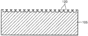
- 1 to 3 are schematic cross-sectional views showing a method of forming a nano pattern according to an embodiment of the present invention.
- FIGS. 4 and 5 are schematic cross-sectional views showing a method of forming a nano pattern according to another embodiment of the present invention.
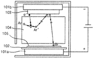
- FIG. 6 is a schematic cross-sectional view showing a sputtering deposition apparatus used in an experimental example of the present invention.
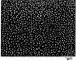
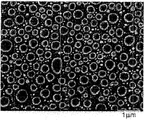
- 7A to 7C are scanning electron microscope (SEM) photographs of a specimen composed of a substrate and bismuth particles formed by sputtering on the substrate.
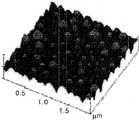
- AFM 8A and 8B are atomic force microscope (AFM) images of a specimen including bismuth particles formed by sputtering on the substrate and the substrate according to the deposition time.
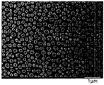
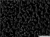
- 9A and 9B are scanning electron microscope (SEM) photographs showing nano-patterns formed by selectively etching a surface of a glass substrate using a mask layer including sputtered bismuth particles and removing the mask layer.
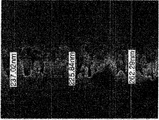
- 10A and 10B are scanning electron microscope (SEM) images showing a cross section of the nanopattern shown in FIGS. 9A and 9B, respectively.
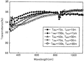
- FIG. 11 is a graph showing light transmittance versus wavelength of light in a nano-patterned glass substrate embodied by another embodiment of the present disclosure.
- 12A to 12D are diagrams showing contact angles of water droplets with substrates under various substrate conditions.
- 12E is a graph illustrating the contact angle between the super water-repellent coating layer and the water droplets in a state where water droplets are formed after the super water-repellent coating is performed on the glass substrate on which the nanopattern is formed.
- 13A and 13B are scanning electron microscope (SEM) photographs of specimens made of a steel sheet substrate and bismuth particles sputtered on the steel sheet substrate.
- 1 to 3 are schematic cross-sectional views showing a method of forming a nano pattern according to an embodiment of the present invention.
- a substrate 105 may be provided, and a mask layer 112 may be formed on the substrate 105.
- the substrate 105 may have various materials according to its use.
- substrate 105 may include a ceramic that partially requires water repellency, oil repellency, or light transmissivity.
- the ceramic may comprise glass.
- the glass substrate may be used as a mask for lithography, or may be used in windows of buildings or automobiles, and soda lime glass substrates such as flat glass may be used.
- the substrate 105 may include a metal that partially requires water repellency or oil repellency.
- the substrate 105 may have a body portion of any material, and may include an inorganic surface portion such as a metal or a ceramic requiring a nano pattern on the body portion.
- the substrate 105 may include a polymer material such as polyimide, polyethylene, or the like.
- the mask layer 112 may be used as an etch protection layer in the etching step of the substrate 105.
- at least the surface portion of the substrate 105 may be formed of a material having an etching selectivity with respect to the mask layer 112.
- the mask layer 112 may have an appropriate thickness, for example, 1 ⁇ m or less in consideration of the burden of patterning.
- the mask layer 112 may include nano-aggregated particles 110 and openings 111 exposing the substrate 105 between the particles 110.
- the nano-aggregated particles 110 may be particles including pure metals and / or alloys, and may be particles including low melting metal materials such as bismuth or tin.
- the material constituting the nano-aggregated particles 110 is not limited to the low melting point metal material described above, and may include any material formed by vapor deposition.
- the nano-aggregated particles 110 may include ceramic material as well as any metal material.
- the nano-aggregated particles 110 may include nano-aggregated particles formed on the substrate 105 using physical vapor deposition (PVD).
- PVD physical vapor deposition
- Physical vapor deposition methods include a method of depositing particles on a substrate by releasing particles from a source (eg, a sputter target or crucible) using thermal or kinetic energy of ions, specifically, the kinetic energy of ions Sputtering method using a, vacuum deposition method using the thermal energy of the ions and the like.
- the physical vapor deposition method may include an ion plating method, in which atoms evaporated from the anode reach a cathode in a charged state and are discharged and attached in a manner similar to electroplating in a gaseous state.
- the nano-aggregated particles 110 continuously and / or discontinuously spaced apart must first be formed on the substrate, followed by nano-aggregation.
- the material layer is formed by the movement, diffusion, growth, and / or condensation of the particles 110.
- the nano-aggregated particles 110 described in the present embodiment include continuous and / or discontinuously spaced nano-aggregated particles formed before the step of forming the material layer by the physical vapor deposition method.
- Nano-aggregated particles 110 may include dynamically stable spontaneous agglomerates formed on substrate 105 in-situ.
- An opening 111 interposed between the nano-aggregated particles 110 may expose the substrate 105.
- the nano-aggregated particles 110 may have a diameter of a nano scale, for example, several to several hundred nm in size, and at least portions may be spaced apart from each other. Thus, the opening 111 may be defined in part or in whole along the boundary of the particles 110.
- the size of the nano-aggregated particles 110 and the size of the opening 111 may have a formal or atypical distribution according to physical vapor deposition conditions.
- the nano-aggregated particles 110 are shown as constituting a single layer on the substrate 105 for convenience, but may be composed of a plurality of layers as well as a single layer.
- the nano-aggregated particles 110 may include nano-aggregated particles formed on the substrate 105 using chemical vapor deposition (CVD).
- CVD chemical vapor deposition
- a reaction gas is introduced into a reactor to form a predetermined material layer on a surface of a substrate by using a reaction between the reaction gases.
- the nano-aggregated particles 110 may include dynamically stable spontaneous aggregates formed on the substrate 105 during in-situ.
- the nano-aggregated particles are thermodynamically spontaneously generated during the deposition process.
- low melting point metal materials such as bismuth or tin have the advantage of being relatively inexpensive.
- metals such as platinum (Pt), palladium (Pd), gold (Au) or silver (Ag) not only have relatively expensive material costs but also do not spontaneously generate thermodynamically during the deposition process and must be subjected to high temperature heat treatment. There is a disadvantage that must cause aggregation through.
- the nano pattern 120 may be formed by etching the surface of the substrate 105 through the opening 111 by using the mask layer 112 as an etch protection layer.
- the etching of the substrate 105 may use plasma dry etch to form the nanopattern 120. If the plasma dry etching has only the characteristics of anisotropic etching, the width of the nanopattern 120 may be equal to the width of the opening 111.
- the width is a concept including the width in the horizontal direction on the drawing.
- plasma dry etching may have anisotropic etching as its main characteristic, but may also have the characteristic of isotropic etching.
- the width of the nanopattern 120 may be larger than the width of the opening 111. This is because the etching also proceeds below the particles 110 through the lateral direction of the opening 111.
- the width according to the depth of the nanopattern 120 may be controlled.
- the width of the nanopattern 120 has the largest width of the inlet of the nanopattern 120 having the same level as the top surface of the substrate 105 and gradually increases toward the bottom surface of the nanopattern 120. Can be controlled to be small.
- etching of the substrate 105 causes hydrofluoric acid (HF) vapor to pass through the opening 111 onto the substrate 105 to form the nanopattern 120.
- HF hydrofluoric acid
- the surface of the substrate 105 can be etched by a chemical dry etch method.
- the etching of the substrate 105 may proceed using wet etching.
- the surface of the substrate 105 may be etched through the opening 111 using a dilute hydrofluoric acid (HF) solution or a buffered oxide etchant (BOE) solution.
- HF dilute hydrofluoric acid
- BOE buffered oxide etchant
- the mask layer 112 may be adjusted to etch little or relatively very slowly compared to the substrate 105. That is, the substrate 105 may be selected to have an etch selectivity with respect to the mask layer 112.
- etching of the substrate 105 may be performed using the mask layer 112 having the nano-aggregated particles 110 in a blanket state without a photo mask. Such etching is easier to process substrates 105 of various shapes and / or large diameters compared to lithography processes.
- the nano-aggregated particles 110 before etching the substrate 105 using the mask layer 112 having the nano-aggregated particles 110, the nano-aggregated particles 110 through heat treatment in air
- the step of oxidizing may be further performed.
- the inventors have found that when the substrate 105 is etched using the mask layer having oxidized nano-aggregated particles, the etching selectivity of the substrate relative to the mask layer becomes relatively higher under the same etching process conditions.
- the mask layer 112 may be removed to leave the nanopattern 120 on the surface of the substrate 105.
- the mask layer 112 may be removed using wet etching.
- the mask layer 112 may be removed using plasma etching.
- the remaining nanopattern 120 may function as a nanostructure on the surface of the substrate 105, and the nanostructure may form a network structure and thus may have durability that does not fall down due to external impact.
- Such nanostructures can be used to control the water repellency, oil repellency or light transmittance of the substrate 105.
- a hydrophobic coating layer may be additionally bonded onto the nanopattern 120.
- the hydrophobic coating layer may be bonded to the nano-pattern 120 by plasma treatment of CHF 3 gas.
- the nano-pattern 120 is formed on the surface of the solar cell, it is possible to increase the light transmittance incident to the solar cell.
- the nanostructure may be used for the purpose of increasing the surface area of the substrate 105.
- the substrate 105 may be used as an electrode of a battery, and the nano pattern 120 may be formed on the substrate 105 to increase the reactivity of the electrode surface.
- the nano pattern 120 may replace a structure such as carbon nanotubes used in the battery electrode.
- 1, 4 and 5 are schematic cross-sectional views showing a method of forming a nano pattern according to another embodiment of the present invention.
- the surface of the substrate 105 is etched through the opening 111 to form a nano-pattern. 120 may be formed.
- the etching of the substrate 105 may use plasma dry etching to form the nanopattern 120. If the plasma dry etching has only the characteristics of anisotropic etching, the width of the nanopattern 120 may be equal to the width of the opening 111.
- the width is a concept including the width in the horizontal direction on the drawing.
- plasma dry etching may have anisotropic etching as a main characteristic, but may also have anisotropic etching characteristics.
- the width of the nanopattern 120 may be larger than the width of the opening 111. This is because the etching also proceeds below the particles 110 through the lateral direction of the opening 111.
- the width according to the depth of the nanopattern 120 may be controlled.
- the width of the nanopattern 120 is gradually increased toward the inside of the substrate 105 at the entrance of the nanopattern 120 having the same level as the upper surface of the substrate 105 to have a maximum width at a predetermined depth.
- the width of the nano-pattern 120 may be controlled to decrease toward the bottom surface of the nano-pattern 120 at the predetermined depth.
- the nano-aggregated particles 110 refers to nano-aggregated particles that are continuously and / or discontinuously spaced apart before the material layer is formed by the vapor deposition method.
- the nano-aggregated particles may refer to nano-aggregated particles continuously and / or discontinuously spaced after the inorganic layer is formed by the vapor deposition method.
- nano-aggregated particles may be implemented by a metal dewetting phenomenon in which a metal layer formed by a vapor deposition method is agglomerated through heat treatment. Even in this case, the nano-aggregated particles may be dynamically stable spontaneous aggregates formed on the substrate 105.
- FIG. 6 is a schematic cross-sectional view showing a sputtering deposition apparatus used in an experimental example of the present invention.
- a sputtering target 103 is disposed on the cathode electrode 101b and a substrate holder portion 102 on the anode electrode 101a.
- the substrate 105 is disposed therebetween.
- Power is supplied between the anode electrode 101a and the cathode electrode 101b to accelerate the ions and electrons toward the sputtering target 103 in the state where the plasma 104 is generated.
- Ar collides with atoms to form ions.
- Nano-aggregated particles 110 may include dynamically stable spontaneous agglomerates formed on substrate 105 in-situ.
- 7A to 7C are scanning electron microscope (SEM) images of specimens composed of bismuth particles formed by sputtering on a glass substrate.
- 7A, 7B, and 7C show specimens formed by depositing bismuth particles at 75 seconds, 100 seconds, and 150 seconds, respectively, under a sputter deposition temperature of 150 ° C., corresponding to the structure shown in FIG. 1. . It can be seen that the longer the deposition time, the larger the size of each of the nano-aggregated particles formed on the substrate.
- AFM atomic force microscope
- FIGS. 8A and 8B illustrate specimens formed by depositing bismuth particles at 75 seconds and 100 seconds, respectively, under a sputter deposition temperature of 150 ° C., which are the same as the specimens shown in FIGS. 7A and 7B, respectively.
- the value Ra of the surface roughness of the nano-aggregated particles formed on the substrate may be increased.
- FIGS. 9A and 9B are scanning electron microscope (SEM) photographs showing nano-patterns formed by selectively etching a surface of a glass substrate using a mask layer including sputtered bismuth particles and removing the mask layer.
- FIG. 10B are scanning electron microscope (SEM) images showing a cross section of the nanopattern shown in FIGS. 9A and 9B, respectively.
- the structure shown in FIGS. 9A and 10A is formed by selectively etching the surface of a glass substrate for 15 minutes using a mask layer containing bismuth particles and removing the mask layer with respect to the specimen shown in FIG. 7A. 9B and 10B, the structure shown in FIGS. 9B and 10B was selectively reactively etched (RIE) the surface of the glass substrate for 30 minutes using a mask layer comprising bismuth particles with respect to the specimen shown in FIG.
- RIE reactively etched
- the formed nanopattern it corresponds to the upper surface or the cross section of the structure shown in FIG. 3 or FIG. 5.
- the shape of the nano-pattern may have a dimple shape or a trench shape, but the technical idea of the present invention is not limited thereto and may have various irregular shapes.
- FIG. 11 is a graph showing light transmittance versus wavelength of light in a nano-patterned glass substrate embodied by another embodiment of the present disclosure.
- the nano-pattern is reactively etched on the surface of the glass substrate selectively for 15 or 30 minutes using a mask layer comprising bismuth particles formed by advancing the deposition time of the bismuth particles on the glass substrate to 50 seconds, 75 seconds or 100 seconds. (RIE) and the mask layer were removed.
- RIE etching bismuth particles formed by advancing the deposition time of the bismuth particles on the glass substrate to 50 seconds, 75 seconds or 100 seconds.
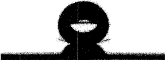
- FIGS 12A to 12D are diagrams showing contact angles of water droplets with substrates under various substrate conditions.
- the contact angle means the angle between the horizontal yellow line and the inclined red line shown in the figure.
- the contact angle between the substrate and the droplets is 39.4 ° while the droplets are formed on the pure glass substrate on which the nano-pattern is not formed.
- water droplets are formed on a nano-pattern (sample of FIG. 9A) formed by plasma etching a glass substrate using a mask layer formed with a deposition time of bismuth particles at 75 seconds under a sputtering deposition temperature of 150 ° C.
- FIG. 12B It can be seen that the contact angle between the nanopattern and the water droplet in this conjunct state is 13.6 °.
- water droplets on a nanopattern (sample of FIG. 9B) implemented by plasma etching a glass substrate using a mask layer formed with a deposition time of bismuth particles at 100 seconds under a sputtering deposition temperature of 150 ° C. It can be seen that the contact angle between the nano-pattern and the water droplet in this conjoined state is 20.0 °.
- the contact angle between the super water-repellent coating layer and the water droplets in the water droplets was found to be very excellent.
- the nano-pattern is reactively etched on the surface of the glass substrate selectively for 15 or 30 minutes using a mask layer comprising bismuth particles formed by advancing the deposition time of the bismuth particles on the glass substrate to 50 seconds, 75 seconds or 100 seconds. (RIE) and the mask layer were removed.
- RIE etching
- the contact angle between the super water-repellent coating layer and the water droplets was measured to be 161.8 ° to 166.7 ° in a state where water droplets were formed after the super water-repellent coating was performed on the glass substrate on which the nano-pattern was formed.
- These super water-repellent properties implemented in glass substrates can be applied to automotive windshields.
- FIGS. 13A and 13B are scanning electron microscope (SEM) photographs of specimens made of a steel sheet substrate and bismuth particles sputtered on the steel sheet substrate.
- SEM scanning electron microscope
- FIGS. 13A and 13B a mask layer including the same nano-aggregated particles may be easily formed on a steel sheet (SUS sheet).
- SUS sheet steel sheet
- the metal substrate can be applied to various applications as long as it can realize surface area increase and water repellency using nano pattern formation. For example, it can be applied in fuel cell and solar cell electrode material using a metal substrate or interior and exterior materials of buildings or automobiles.
Landscapes
- Chemical & Material Sciences (AREA)
- Engineering & Computer Science (AREA)
- Organic Chemistry (AREA)
- Chemical Kinetics & Catalysis (AREA)
- Materials Engineering (AREA)
- General Physics & Mathematics (AREA)
- Metallurgy (AREA)
- Physics & Mathematics (AREA)
- Mechanical Engineering (AREA)
- Manufacturing & Machinery (AREA)
- Inorganic Chemistry (AREA)
- Life Sciences & Earth Sciences (AREA)
- General Chemical & Material Sciences (AREA)
- Geochemistry & Mineralogy (AREA)
- Nanotechnology (AREA)
- Analytical Chemistry (AREA)
- Microelectronics & Electronic Packaging (AREA)
- Physical Vapour Deposition (AREA)
Description
본 발명은 기판의 표면 처리 방법에 관한 것으로서, 특히 기판 상에 나노 패턴을 형성하는 방법 및 이에 의해 제조된 나노 구조물에 관한 것이다.
기판의 표면 처리는 다양한 목적으로 이루어지고 있다. 예를 들어, 기판 표면상에 나노 패턴을 형성함으로써, 기판의 발수성, 발유성, 광투과도 등을 조절할 수 있다. 예를 들어, 연꽃잎의 발수성은 연꽃잎의 표면에 형성된 나노 패턴과 관련되어 있음이 알려져 있다. 다른 예로, 유리 기판 상에 나노 패턴을 형성하고, 그 나노 패턴의 듀티비(duty ratio)를 조절함으로써 유리 기판의 광투과성을 조절할 수 있다.
하지만, 통상적으로 기판 상에 나노 패턴을 형성하기 위해서는, 나노 마스크를 이용한 리소그래피 공정이 필요하다. 나노 마스크는 고가의 전자빔 또는 이온빔 장치를 이용하여 제작되고, 리소그래피 공정은 복잡한 사진 공정을 필요로 한다. 나아가, 나노 패턴은 쉽게 무너지는 문제가 있다.
이에, 본 발명의 일 과제는 내구성이 우수한 나노 패턴 및 그 경제적인 형성 방법을 제공하는 것이다. 이러한 과제는 예시적으로 제시되었고, 본 발명의 범위가 이러한 과제에 의해서 제한되는 것은 아니다.
본 발명의 일 관점에 따른 나노 패턴의 형성방법이 제공된다. 기판 상에 기상 증착법을 이용하여 나노 응집 입자들을 포함하는 마스크층을 형성한다. 상기 마스크층은 상기 나노 응집 입자들 사이로 상기 기판을 노출하는 개구를 갖는다. 상기 마스크층을 식각 보호층으로 이용하여 상기 개구로부터 노출된 상기 기판의 표면을 선택적으로 식각하여, 상기 기판 상에 나노 패턴을 형성한다. 상기 나노 응집 입자들은 상기 기상 증착법을 이용하여 상기 기판 상에 자발적으로 생성되며 열역학적으로 안정한 응결체이고, 상기 나노 응집 입자들을 형성하기 위하여 별도의 열처리를 수반하지 않는다.
상기 나노 패턴의 형성방법에서 상기 나노 패턴을 형성하는 단계 후 상기 마스크층을 제거할 수 있다.
상기 나노 패턴의 형성방법에서 상기 마스크층은 화학적 기상 증착법 또는 물리적 기상 증착 방법을 이용하여 상기 기판 상에 형성된 나노 응집 입자들을 포함할 수 있다.
상기 물리적 기상 증착 방법은 스퍼터링 방법, 진공 증착 방법 및 이온 플레이팅 방법 중 어느 하나 이상을 포함할 수 있다.
상기 나노 패턴의 형성방법에서 상기 기판은 유리, 세라믹, 금속 또는 고분자 재료를 포함할 수 있고, 상기 나노 응집 입자는 금속 또는 세라믹을 포함할 수 있다.
이때 상기 금속은 비스무스(bismuth) 또는 주석(tin)을 포함할 수 있다. 나아가, 상기 금속은 열처리를 통하여 형성된 금속 산화물을 포함할 수 있다.
상기 나노 패턴의 형성방법에서 상기 식각은 플라즈마를 이용하는 식각을 포함할 수 있다.
상기 나노 패턴의 형성방법에서 상기 식각은 불소 증기를 이용하는 식각을 포함할 수 있다.
상기 나노 패턴의 형성방법에서 상기 기판의 표면을 선택적으로 식각하는 단계는 상기 나노 패턴의 폭이 상기 개구의 폭보다 커지도록 수행할 수 있다.
본 발명의 다른 관점에 따른 나노 구조물이 제공된다. 상기 나노 구조물은 전술한 형성방법에 의하여 제조된 나노 패턴을 포함한다. 상기 나노 패턴의 폭은 상기 나노 패턴을 제조하기 위한 상기 개구의 폭보다 클 수 있다.
본 발명의 일 실시예에 따른 나노 패턴의 형성 방법에 따르면, 기상 증착 방법에 의하여 형성된 나노 응집 입자들을 갖는 마스크층을 식각 보호막으로 이용함으로써 나노 마스크 및 리소그래피 공정 없이 나노 패턴을 형성할 수 있다. 이와 같이, 물리적 기상 증착 방법에 의하여 형성된 나노 응집 입자들을 갖는 마스크층을 이용하여 나노 패턴을 형성하는 방법은 통상적인 리소그래피 공정에 비해서 다양한 형상 및/또는 대구경의 기판의 처리에 용이하다. 이와 같이 형성된 나노 패턴은 네트워크 구조를 갖고 있어서, 나노 돌기 패턴에 비해서 내구성이 우수하다.
도 1 내지 도 3은 본 발명의 일 실시예에 따른 나노 패턴의 형성 방법을 보여주는 개략적인 단면도들이다.
도 4 및 도 5는 본 발명의 다른 실시예에 따른 나노 패턴의 형성 방법을 보여주는 개략적인 단면도들이다.
도 6은 본 발명의 일 실험예에 사용되는 스퍼터링 증착 장치를 보여주는 개략적인 단면도이다.
도 7a 내지 도 7c는 기판 및 기판 상에 스퍼터링 되어 형성된 비스무스 입자들로 구성된 시편의 주사전자현미경(SEM) 사진들이다.
도 8a 및 도 8b는 증착시간에 따라 기판 및 기판 상에 스퍼터링 되어 형성된 비스무스 입자들로 구성된 시편의 원자현미경(AFM) 사진들이다.
도 9a 및 도 9b는 스퍼터링 되어 형성된 비스무스 입자들을 포함하는 마스크층을 사용하여 유리 기판의 표면을 선택적으로 식각하고 마스크층을 제거하여 형성한 나노 패턴을 나타낸 주사전자현미경(SEM) 사진들이다.
도 10a 및 도 10b는 각각 도 9a 및 도 9b에 도시한 나노 패턴의 단면을 나타낸 주사전자현미경(SEM) 사진들이다.
도 11은 본원의 다른 실시예에 의하여 구현된 나노 패턴이 형성된 유리 기판에서 광의 파장에 대한 광투과도를 나타낸 그래프이다.
도 12a 내지 도 12d는 다양한 기판의 조건 하에서 기판과 물방울의 접촉각을 도시하는 도면들이다.
도 12e는 나노 패턴이 형성된 유리 기판 상에 초발수 코팅을 수행한 후에 물방울이 맺힌 상태에서 초발수 코팅층과 물방울 간의 접촉각을 도해하는 그래프이다.
도 13a 및 도 13b는 스틸 강판 기판 및 스틸 강판 기판 상에 스퍼터링 되어 형성된 비스무스 입자들로 구성된 시편의 주사전자현미경(SEM) 사진들이다.
이하, 첨부한 도면을 참조하여 본 발명에 따른 바람직한 실시예를 설명함으로써 본 발명을 상세하게 설명한다. 그러나 본 발명은 이하에서 개시되는 실시예에 한정되는 것이 아니라 서로 다른 다양한 형태로 구현될 것이며, 단지 본 실시예는 본 발명의 개시가 완전하도록 하며, 통상의 지식을 가진 자에게 발명의 범주를 완전하게 알려주기 위해 제공되는 것이다. 도면에서 구성 요소들은 설명의 편의를 위하여 그 크기가 과장 또는 축소될 수 있다.
본 발명은 출원인에 의하여 2012년 4월 24일자로 한국특허청에 출원한 출원번호 제10-2012-0042492호에 대하여 우선권을 주장하며, 상기 특허출원의 내용은 전체로서 본 명세서에 인용되어 통합된다.
도 1 내지 도 3은 본 발명의 일 실시예에 따른 나노 패턴의 형성 방법을 보여주는 개략적인 단면도들이다.
도 1을 참조하면, 기판(105)이 제공되고, 기판(105) 상에 마스크층(112)을 형성할 수 있다. 기판(105)은 그 용도에 따라서 다양한 재질을 가질 수 있다. 예를 들어, 기판(105)은 발수성, 발유성 또는 광투과성을 부분적으로 필요로 하는 세라믹을 포함할 수 있다. 상기 세라믹은 유리를 포함할 수 있다. 예컨대, 유리 기판은 리소그래피용 마스크로 이용되거나, 건물 또는 자동차의 창문에 이용될 수 있고, 판유리와 같은 소다라임 유리 기판이 이용될 수 있다. 다른 예로, 기판(105)은 발수성 또는 발유성을 부분적으로 필요로 하는 금속을 포함할 수 있다. 또 다른 예로, 기판(105)은 임의의 재질의 바디부를 갖고, 그 바디부 상에 나노 패턴을 필요로 하는 금속 또는 세라믹과 같은 무기물 표면부를 포함할 수 있다. 또 다른 예로서, 기판(105)은 폴리이미드, 폴리에틸렌 등과 같은 고분자 재료를 포함할 수 있다.
마스크층(112)은 기판(105)의 식각 단계에서 식각 보호층으로 이용될 수 있다. 이러한 의미에서, 기판(105)의 적어도 표면부는 마스크층(112)과 식각 선택비를 갖는 물질로 형성될 수 있다. 마스크층(112)은 패터닝의 부담을 고려하여 적절한 두께, 예컨대 1㎛ 이하의 두께를 가질 수 있다.
예를 들어, 마스크층(112)은 나노 응집 입자들(110)과, 그 입자들(110) 사이로 기판(105)을 노출하는 개구(111)를 포함할 수 있다. 나노 응집 입자들(110)은 순수한 금속 및/또는 합금을 포함하는 입자들이며, 예를 들어, 비스무스(bismuth) 또는 주석(tin)과 같은 저융점 금속 물질을 포함하는 입자들일 수 있다. 그러나, 나노 응집 입자들(110)을 구성하는 물질은 상술한 저융점 금속 물질에 한정되지 않으며, 기상 증착법(vapor deposition)에 의하여 형성되는 임의의 물질을 포함할 수 있다. 예를 들어, 나노 응집 입자들(110)은 임의의 금속 물질 뿐만 아니라 세라믹 물질도 포함할 수 있다.
나노 응집 입자들(110)은 물리적 기상 증착 방법(Physical vapor deposition, PVD)을 이용하여 기판(105) 상에 형성된 나노 응집 입자들을 포함할 수 있다. 물리적 기상 증착 방법은 이온들의 열에너지 또는 운동에너지를 이용하여 소스(예를 들어, 스퍼터 타겟이나 도가니)로부터 입자들을 방출시켜 기판 상에 상기 입자들을 증착하는 방법을 포함하며, 구체적으로, 이온들의 운동에너지를 이용하는 스퍼터링 방법, 이온들의 열에너지를 이용하는 진공 증착 방법 등으로 분류될 수 있다. 이외에도 물리적 기상 증착 방법은 기상 상태 속의 전기도금과 비슷한 방식으로 양극에서 증발된 원자가 대전된 상태로 음극에 도달하여 방전되어 부착되는 방법인 이온 플레이팅 방법을 포함할 수 있다.
기판 상에 물리적 기상 증착 방법에 의하여 물질층이 형성되는 과정을 가정하여 살펴보면, 기판 상에 연속적으로 및/또는 불연속적으로 이격된 나노 응집 입자들(110)들이 우선 형성되어야 하며, 계속하여 나노 응집 입자들(110)이 이동, 확산, 성장 및/또는 응축(condensation)됨으로써 물질층이 형성된다. 본 실시예에서 설명하는 나노 응집 입자들(110)은 물리적 기상 증착 방법에 의하여 물질층이 형성되는 단계 이전(以前)에 형성된 연속적으로 및/또는 불연속적으로 이격된 나노 응집 입자들을 포함한다. 나노 응집 입자들(110)은 증착 중(in-situ)에 기판(105) 상에 형성되는 역학적으로 안정한 자발적인 응결체를 포함할 수 있다.
나노 응집 입자들(110) 사이에 개재되는 개구(111)는 기판(105)을 노출시킬 수 있다. 나노 응집 입자들(110)은 나노 스케일, 예컨대 수 내지 수백 nm 크기의 직경을 갖고, 적어도 일부분들이 서로 이격되게 형성될 수 있다. 따라서 입자들(110)의 경계를 따라서 부분적으로 또는 전체적으로 개구(111)가 한정될 수 있다. 나노 응집 입자들(110)의 크기와 개구(111)의 크기는 물리적 기상 증착 조건에 따라 정형적 또는 비정형적인 분포를 가질 수 있다. 도면에서는 편의상 나노 응집 입자들(110)이 기판(105) 상에서 단일층을 구성하는 것으로 도시하였으나, 단일층 뿐만 아니라 복수의 층으로 구성될 수도 있다.
본 발명의 변형된 실시예에서, 나노 응집 입자들(110)은 화학적 기상 증착 방법(Chemical vapor deposition, CVD)을 이용하여 기판(105) 상에 형성된 나노 응집 입자들을 포함할 수 있다. 화학적 기상 증착 방법은 반응 가스를 반응기 내부로 투입하여 상기 반응 가스 간의 반응을 이용하여 기판의 표면에 소정의 물질층을 형성하는 방법이다. 화학적 기상 증착 방법에 의해 물질층을 형성하는 경우에도 물리적 기상 증착 방법과 마찬가지로 물질층이 형성되는 단계 이전(以前)에 형성된 연속적으로 및/또는 불연속적으로 이격된 나노 응집 입자들이 형성될 수 있다. 이 경우, 나노 응집 입자들(110)은 증착 중(in-situ)에 기판(105) 상에 형성되는 역학적으로 안정한 자발적인 응결체를 포함할 수 있다.
앞에서 설명한 것처럼, 본 발명의 주요한 기술적 사상들 중 하나는 상기 나노 응집 입자들이 증착 공정 중 열역학적으로 자발적으로 생성된다는 것이다. 특히 비스무스(bismuth) 또는 주석(tin)과 같은 저융점 금속 물질은 상대적으로 저가인 장점을 가진다. 반면에, 백금(Pt), 팔라듐(Pd), 금(Au) 또는 은(Ag)과 같은 금속은 상대적으로 고가의 재료비가 소요될 뿐만 아니라 증착 공정 중 열역학적으로 자발적으로 생성되지 않고 반드시 고온의 열처리를 통하여 응집을 일으켜야 하는 단점이 있다.
도 1 및 도 2를 참조하면, 마스크층(112)을 식각 보호막으로 이용하여, 개구(111)를 통해서 기판(105)의 표면을 식각하여, 나노 패턴(120)을 형성할 수 있다. 예를 들어, 기판(105)의 식각은 나노 패턴(120)을 형성하도록 플라즈마 건식 식각(plasma dry etch)을 이용할 수 있다. 플라즈마 건식 식각이 이방성 식각(anisotropic etch)의 특성만을 가진다면 나노 패턴(120)의 폭은 개구(111)의 폭과 동일할 것이다. 여기에서, 폭이라 함은 도면상에서 가로 방향의 폭을 포함하는 개념이다.
한편, 공정 조건에 따라서 플라즈마 건식 식각은 이방성 식각을 주요한 특성으로 가지나 등방성 식각(isotropic etch)의 특성도 부차적으로 가질 수 있다. 이 경우에는, 나노 패턴(120)의 폭은 개구(111)의 폭보다 커질 수 있다. 왜냐하면, 식각이 개구(111)의 측방향을 통해서 입자들(110) 아래로도 진행되기 때문이다.
이방성 식각과 등방성 식각의 특성이 적절하게 나타나도록 플라즈마 건식 식각의 조건을 설정하면, 나노 패턴(120)의 깊이에 따른 폭이 제어될 수 있다. 예를 들어, 나노 패턴(120)의 폭은 기판(105)의 상부면과 동일한 레벨을 가지는 나노 패턴(120)의 입구의 폭이 가장 크며 나노 패턴(120)의 바닥면으로 향할수록 폭이 점점 작아지도록 제어될 수 있다.
다른 변형된 실시예에서, 기판(105)이 유리 기판인 경우, 기판(105)의 식각은 나노 패턴(120)을 형성하도록 불산(HF) 증기를 개구(111)를 통해서 기판(105) 상으로 제공함으로써 기판(105)의 표면을 화학적 건식 식각(chemical dry etch)법으로 식각할 수 있다.
또 다른 변형된 실시예에서, 기판(105)의 식각은 습식 식각을 이용하여 진행할 수도 있다. 예컨대, 희석된 불산(HF) 용액 또는 BOE(Buffered Oxide Etchant) 용액을 이용하여 개구(111)를 통해서 기판(105)의 표면을 식각할 수도 있다. 습식 식각은, 플라즈마나 불산 증기를 이용하는 건식 식각과 달리, 나노 응집 입자들(110)이 기판(105)으로부터 분리되지 않도록 그 시간 및 조건을 조절하여 적용될 필요가 있다.
이러한 식각 동안, 마스크층(112)은 기판(105)에 비해서 거의 식각이 되지 않거나 상대적으로 매우 느리게 식각되도록 조절될 수 있다. 즉, 기판(105)은 마스크층(112)에 대해서 식각 선택비를 갖도록 선택될 수 있다.
이와 같이 본 발명에 의할 경우, 기판(105) 식각은 포토 마스크 없이 블랭킷(blanket) 상태에서 나노 응집 입자들(110)을 갖는 마스크층(112)을 이용하여 수행할 수 있다. 이러한 식각은 리소그래피 공정에 비해서 다양한 형상 및/또는 대구경의 기판(105)의 처리에 용이하다.
한편, 본 발명의 변형된 실시예에서, 나노 응집 입자들(110)을 갖는 마스크층(112)을 이용하여 기판(105)을 식각하기 이전에, 공기 중 열처리를 통해 나노 응집 입자들(110)을 산화하는 단계를 더 수행할 수 있다. 발명자는 산화된 나노 응집 입자들을 갖는 마스크층을 이용하여 기판(105)을 식각하는 경우, 동일한 식각공정 조건에서, 마스크층에 대한 기판의 식각선택비가 상대적으로 더 높아지는 것을 확인하였다. 예를 들어, 유리 기판 상에 증착된 비스무스를 산화시켜 BiOx 형태의 산화물을 가지는 마스크층을 이용하는 경우에, 산화시키지 않은 비스무스 나노 응집 입자들을 갖는 마스크층을 이용하는 경우에 비하여, 동일한 식각공정 조건에서, 식각선택비가 더 높아지는 것을 확인하였다. 또한, 금속 기판에서도 산화물 형태의 나노 응집 입자들을 갖는 마스크층을 이용하는 경우 습식 또는 건식 식각시 더욱 높은 식각선택비가 나타남을 확인하였다.
도 3을 참조하면, 마스크층(112)을 제거하여, 기판(105) 표면 상에 나노 패턴(120)을 잔류시킬 수 있다. 예를 들어, 마스크층(112)은 습식 식각을 이용하여 제거할 수 있다. 다른 예로, 마스크층(112)은 플라즈마 식각을 이용하여 제거할 수도 있다. 잔류된 나노 패턴(120)은 기판(105) 표면 상의 나노 구조물로 기능할 수 있고, 이러한 나노 구조물은 네트워크 구조를 이루고 있어서 외부 충격 등에 의해서 잘 쓰러지지 않는 내구성을 가질 수 있다.
이러한 나노 구조물은 기판(105)의 발수성, 발유성 또는 광투과성을 조절하는 데 이용될 수 있다. 예를 들어, 발수성을 높이기 위해서, 나노 패턴(120) 상에 소수성 코팅층을 부가적으로 결합시킬 수 있다. 예컨대, 소수성 코팅층은 CHF3 기체를 플라즈마 처리하여 나노 패턴(120) 상에 결합시킬 수 있다. 한편, 태양 전지의 표면에 이러한 나노 패턴(120)을 형성하는 경우, 태양 전지로 입사되는 광투과도를 높일 수도 있다.
한편, 나노 구조물은 기판(105)의 표면적을 늘리는 목적으로 이용될 수도 있다. 예를 들어, 기판(105)은 배터리의 전극으로 이용될 수 있고, 전극 표면의 반응성을 높이기 위해서 나노 패턴(120)이 기판(105) 상에 형성될 수도 있다. 이에 따라, 이러한 나노 패턴(120)은 배터리 전극에 사용되는 탄소나노튜브(carbon nanotube)와 같은 구조를 대체할 수도 있다.
도 1, 도 4 및 도 5는 본 발명의 다른 실시예에 따른 나노 패턴의 형성 방법을 보여주는 개략적인 단면도들이다.
도 1, 도 4 및 도 5를 참조하면, 본 발명의 다른 실시예에서, 마스크층(112)을 식각 보호막으로 이용하여, 개구(111)를 통해서 기판(105)의 표면을 식각하여, 나노 패턴(120)을 형성할 수 있다. 예를 들어, 기판(105)의 식각은 나노 패턴(120)을 형성하도록 플라즈마 건식 식각을 이용할 수 있다. 플라즈마 건식 식각이 이방성 식각의 특성만을 가진다면 나노 패턴(120)의 폭은 개구(111)의 폭과 동일할 것이다. 여기에서, 폭이라 함은 도면상에서 가로 방향의 폭을 포함하는 개념이다.
한편, 공정 조건에 따라서 플라즈마 건식 식각은 이방성 식각을 주요한 특성으로 가지나 등방성 식각의 특성도 부차적으로 가질 수 있다. 이 경우에는, 나노 패턴(120)의 폭은 개구(111)의 폭보다 커질 수 있다. 왜냐하면, 식각이 개구(111)의 측방향을 통해서 입자들(110) 아래로도 진행되기 때문이다.
이방성 식각과 등방성 식각의 특성이 적절하게 나타나도록 플라즈마 건식 식각의 조건을 설정하면, 나노 패턴(120)의 깊이에 따른 폭이 제어될 수 있다. 예를 들어, 나노 패턴(120)의 폭은 기판(105)의 상부면과 동일한 레벨을 가지는 나노 패턴(120)의 입구에서 기판(105)의 내부로 향할수록 점점 커져 소정의 깊이에서 최대폭을 가지다가, 상기 소정의 깊이에서 다시 나노 패턴(120)의 바닥면으로 향할수록 나노 패턴(120)의 폭이 점점 작아지도록 제어될 수 있다. 이러한 형상을 가지는 나노 패턴(120) 상에 초발수 코팅층을 형성하는 경우 외부 충격으로부터 초발수 코팅층을 구조적으로 보호할 수 있는 효과를 기대할 수 있다. 나노 패턴(120) 이외의 다른 구성요소들에 대한 설명은 도 1 내지 도 3에서 설명한 구성요소들과 동일하여 중복되므로, 여기에서는 설명을 생략한다.
한편, 상술한 실시예들에서, 나노 응집 입자들(110)은 기상 증착 방법에 의하여 물질층이 형성되는 단계 이전(以前)에 형성된 연속적으로 및/또는 불연속적으로 이격된 나노 응집 입자들을 의미하였으나, 본원의 변형된 실시예에서, 나노 응집 입자들은 기상 증착 방법에 의하여 무기물층이 형성되는 단계 이후(以後)에 형성된 연속적으로 및/또는 불연속적으로 이격된 나노 응집 입자들을 의미할 수 있다. 예를 들어, 기상 증착 방법에 의하여 형성된 금속층을 열처리를 통하여 응집(agglomeration)시키는 금속 디웨팅(metal dewetting) 현상에 의하여 나노 응집 입자들을 구현할 수도 있다. 이 경우에도, 나노 응집 입자들은 기판(105) 상에 형성되는 역학적으로 안정한 자발적인 응결체일 수 있다.
이하에서는, 본 발명의 다양한 실험예들을 들어, 본 발명을 보다 구체적으로 설명한다. 다만, 하기의 실험예들은 본 발명의 이해를 돕기 위한 것일 뿐, 본 발명이 아래의 실험예들에 의해서 한정되는 것은 아니다.
도 6은 본 발명의 일 실험예에 사용되는 스퍼터링 증착 장치를 보여주는 개략적인 단면도이다.
도 6을 참조하면, 애노드 전극(101a)과 캐소드 전극(101b)이 서로 마주보는 상태에서, 캐소드 전극(101b)에는 스퍼터링 타겟(103)이 배치되고 애노드 전극(101a)에는 기판 홀더부(102)가 개재되어 기판(105)이 배치된다. 애노드 전극(101a)과 캐소드 전극(101b) 사이에 전원을 공급하여 플라즈마(104)가 발생된 상태에서 스퍼터링 타겟(103)을 향한 가속된 이온, 전자들이 비활성 가스의 원자(예를 들어, 아르곤(Ar) 원자)와 충돌하여 이온들이 형성된다. 계속하여, 상기 이온들이 스퍼터링 타겟(103)에 충돌함으로써 스퍼터링 타겟(103)의 원자들이 방출되고 기판(105)을 향하여 스퍼터링 타겟(103)의 원자들이 이송하여 기판(105) 상에 형성된다. 기판(105) 상에 형성된 스퍼터링 타겟(103)의 원자들은 도 1에 도시된 나노 응집 입자들(110)에 해당한다. 나노 응집 입자들(110)은 증착 중(in-situ)에 기판(105) 상에 형성되는 역학적으로 안정한 자발적인 응결체를 포함할 수 있다.
도 7a 내지 도 7c는 유리 기판 상에 스퍼터링 되어 형성된 비스무스 입자들로 구성된 시편의 주사전자현미경(SEM) 사진들이다.
도 7a, 도 7b 및 도 7c는 스퍼터링 증착온도가 150℃인 조건 하에서 비스무스 입자의 증착시간을 각각 75초, 100초 및 150초로 하여 형성한 시편을 나타낸 것으로서, 도 1에 도시된 구조체에 대응된다. 증착시간이 길수록 기판 상에 형성된 나노 응집 입자의 각각의 크기는 커짐을 확인할 수 있다.
도 8a 및 도 8b는 증착시간에 따라 유리 기판 상에 스퍼터링 되어 형성된 비스무스 입자들로 구성된 시편의 원자현미경(AFM) 사진들이다.
도 8a 및 도 8b는 스퍼터링 증착온도가 150℃인 조건 하에서 비스무스 입자의 증착시간을 각각 75초 및 100초로 하여 형성한 시편을 나타낸 것으로서, 도 7a 및 도 7b에 나타난 시편과 각각 동일하다. 증착시간이 길수록 기판 상에 형성된 나노 응집 입자들의 표면 거칠기의 값(Ra)은 커짐을 확인할 수 있다.
도 9a 및 도 9b는 스퍼터링 되어 형성된 비스무스 입자들을 포함하는 마스크층을 사용하여 유리 기판의 표면을 선택적으로 식각하고 마스크층을 제거하여 형성한 나노 패턴을 나타낸 주사전자현미경(SEM) 사진들이며, 도 10a 및 도 10b는 각각 도 9a 및 도 9b에 도시한 나노 패턴의 단면을 나타낸 주사전자현미경(SEM) 사진들이다.
도 9a 및 도 10a에 나타난 구조체는 도 7a에 나타난 시편에 대하여 비스무스 입자들을 포함하는 마스크층을 사용하여 유리 기판의 표면을 선택적으로 15분 동안 반응성 식각(RIE)하고 마스크층을 제거하여 형성한 나노 패턴이며, 도 9b 및 도 10b에 나타난 구조체는 도 7a에 나타난 시편에 대하여 비스무스 입자들을 포함하는 마스크층을 사용하여 유리 기판의 표면을 선택적으로 30분 동안 반응성 식각(RIE)하고 마스크층을 제거하여 형성한 나노 패턴으로서, 도 3 또는 도 5에 도시된 구조체의 상부면 또는 단면에 대응된다. 나노 패턴의 형상은 딤플 형상이나 트렌치 형상을 가질 수 있으나, 본 발명의 기술적 사상은 이에 한정되지 않으며 다양한 비정형의 형상을 가질 수도 있다.
도 11은 본원의 다른 실시예에 의하여 구현된 나노 패턴이 형성된 유리 기판에서 광의 파장에 대한 광투과도를 나타낸 그래프이다. 나노 패턴은 유리 기판 상에 비스무스 입자의 증착시간을 50초, 75초 또는 100초로 진행하여 형성한 비스무스 입자들을 포함하는 마스크층을 사용하여 유리 기판의 표면을 선택적으로 15분 또는 30분 동안 반응성 식각(RIE)하고 마스크층을 제거하여 형성하였다. 도 11을 참조하면, 표면의 나노 패턴 형성으로 기인한 반사도 감소로 인하여, 유리 기판의 광투과도 개선효과를 확인할 수 있다. 통상의 경우 유리의 광투과도는 가시광 영역에서 92% 수준이나, 도 11과 같이, 본원의 다른 실시예에 의한 나노 패턴 형성 후의 유리 기판의 광투과도는 92% 이상이며 가시광 평균 94% 내지 96% 수준으로 향상됨을 확인할 수 있다.
도 12a 내지 도 12d는 다양한 기판의 조건 하에서 기판과 물방울의 접촉각을 도시하는 도면들이다. 접촉각은 도면에서 도시된 수평한 노란선과 기울어진 붉은선 사이의 각을 의미한다.
도 12a를 참조하면, 나노 패턴이 형성되지 않은 순수한 유리 기판 상에 물방울이 맺힌 상태에서 기판과 물방울 간의 접촉각은 39.4°임을 확인할 수 있다.
도 12b를 참조하면, 스퍼터링 증착온도가 150℃인 조건 하에서 비스무스 입자의 증착시간을 75초로 하여 형성한 마스크층을 사용하여 유리 기판을 플라즈마 식각하여 구현한 나노 패턴(도 9a의 시편) 상에 물방울이 맺힌 상태에서 나노 패턴과 물방울 간의 접촉각은 13.6°임을 확인할 수 있다.
도 12c를 참조하면, 스퍼터링 증착온도가 150℃인 조건 하에서 비스무스 입자의 증착시간을 100초로 하여 형성한 마스크층을 사용하여 유리 기판을 플라즈마 식각하여 구현한 나노 패턴(도 9b의 시편) 상에 물방울이 맺힌 상태에서 나노 패턴과 물방울 간의 접촉각은 20.0°임을 확인할 수 있다.
도 12d를 참조하면, 나노 패턴이 형성된 유리 기판 상에 초발수 코팅을 수행한 후에 물방울이 맺힌 상태에서 초발수 코팅층과 물방울 간의 접촉각을 확인한 결과 매우 우수한 초발수 특성이 나타남을 확인할 수 있었다. 나노 패턴은 유리 기판 상에 비스무스 입자의 증착시간을 50초, 75초 또는 100초로 진행하여 형성한 비스무스 입자들을 포함하는 마스크층을 사용하여 유리 기판의 표면을 선택적으로 15분 또는 30분 동안 반응성 식각(RIE)하고 마스크층을 제거하여 형성하였다. 도 12e를 참조하면, 나노 패턴이 형성된 유리 기판 상에 초발수 코팅을 수행한 후에 물방울이 맺힌 상태에서 초발수 코팅층과 물방울 간의 접촉각은 161.8°내지 166.7°인 것으로 측정되었으며 매우 우수한 초발수 특성이 나타남을 확인할 수 있었다. 유리 기판에서 구현된 이러한 초발수 특성은 자동차 유리창에 적용될 수 있다.
도 13a 및 도 13b는 스틸 강판 기판 및 스틸 강판 기판 상에 스퍼터링 되어 형성된 비스무스 입자들로 구성된 시편의 주사전자현미경(SEM) 사진들이다. 앞에서는 주로 유리 기판 상에 나노 응집 입자들을 포함하는 마스크층을 형성하는 실시예들을 설명하였으나, 본 발명의 기술적 사상이 이에 한정되지 않음은 명백하다. 예를 들어, 도 13a 및 도 13b와 같이, 스틸 강판(SUS 강판) 상에서도 동일한 나노 응집 입자들을 포함하는 마스크층이 용이하게 형성될 수 있다. 금속 기판에서도 나노 패턴 형성을 이용한 표면적증가와 발수특성을 구현할 수 있다면 다양한 용도로 적용될 것으로 기대된다. 예를 들어, 금속 기판을 이용한 연료전지 및 태양전지 전극물질 또는 건물이나 자동차의 내외장재에서 적용될 수 있다.
발명의 특정 실시예들에 대한 이상의 설명은 예시 및 설명을 목적으로 제공되었다. 따라서 본 발명은 상기 실시예들에 한정되지 않으며, 본 발명의 기술적 사상 내에서 해당 분야에서 통상의 지식을 가진 자에 의하여 상기 실시예들을 조합하여 실시하는 등 여러 가지 많은 수정 및 변경이 가능함은 명백하다.
Claims (11)
- 기판 상에 기상 증착법을 이용하여 나노 응집 입자들을 포함하는 마스크층을 형성하되, 상기 마스크층은 상기 나노 응집 입자들 사이로 상기 기판을 노출하는 개구를 갖는, 상기 마스크층을 형성하는 단계; 및상기 마스크층을 식각 보호층으로 이용하여 상기 개구로부터 노출된 상기 기판의 표면을 선택적으로 식각하여, 상기 기판 상에 나노 패턴을 형성하는 단계를 포함하며,상기 나노 응집 입자들은 상기 기상 증착법을 이용하여 상기 기판 상에 자발적으로 생성되며 열역학적으로 안정한 응결체이고,상기 나노 응집 입자들을 형성하기 위하여 별도의 열처리를 수반하지 않는 것을 특징으로 하는,나노 패턴의 형성방법.
- 제 1 항에 있어서,상기 나노 패턴을 형성하는 단계 후 상기 마스크층을 제거하는 단계를 더 포함하는, 나노 패턴의 형성방법.
- 제 1 항에 있어서,상기 마스크층은 화학적 기상 증착법 또는 물리적 기상 증착 방법을 이용하여 상기 기판 상에 형성된 나노 응집 입자들을 포함하는, 나노 패턴의 형성방법.
- 제 3 항에 있어서,상기 물리적 기상 증착 방법은 스퍼터링 방법, 진공 증착 방법 및 이온 플레이팅 방법 중 어느 하나 이상을 포함하는, 나노 패턴의 형성방법.
- 제 1 항에 있어서,상기 기판은 유리, 세라믹, 금속 및 고분자 재료를 포함하는, 나노 패턴의 형성방법.
- 제 1 항에 있어서,상기 나노 응집 입자는 금속 또는 세라믹을 포함하는, 나노 패턴의 형성방법.
- 제 6 항에 있어서,상기 금속은 비스무스(bismuth) 또는 주석(tin)을 포함하는, 나노 패턴의 형성방법.
- 제 7 항에 있어서,상기 금속은 상기 비스무스 또는 주석을 열처리하여 형성된 금속산화물을 포함하는, 나노 패턴의 형성방법.
- 제 1 항에 있어서,상기 식각은 플라즈마를 이용하는 식각을 포함하는, 나노 패턴의 형성방법.
- 제 1 항에 있어서,상기 식각은 불소 증기를 이용하는 식각을 포함하는, 나노 패턴의 형성방법.
- 제 1 항에 있어서,상기 기판의 표면을 선택적으로 식각하는 단계는 상기 나노 패턴의 폭이 상기 개구의 폭보다 커지도록 수행하는, 나노 패턴의 형성방법.
Applications Claiming Priority (4)
| Application Number | Priority Date | Filing Date | Title |
|---|---|---|---|
| KR10-2012-0042492 | 2012-04-24 | ||
| KR20120042492 | 2012-04-24 | ||
| KR10-2012-0081787 | 2012-07-26 | ||
| KR1020120081787A KR101217783B1 (ko) | 2012-04-24 | 2012-07-26 | 나노 패턴의 형성방법 |
Publications (1)
| Publication Number | Publication Date |
|---|---|
| WO2013162174A1 true WO2013162174A1 (ko) | 2013-10-31 |
Family
ID=47841001
Family Applications (1)
| Application Number | Title | Priority Date | Filing Date |
|---|---|---|---|
| PCT/KR2013/002176 Ceased WO2013162174A1 (ko) | 2012-04-24 | 2013-03-18 | 나노 패턴의 형성방법 |
Country Status (2)
| Country | Link |
|---|---|
| KR (1) | KR101217783B1 (ko) |
| WO (1) | WO2013162174A1 (ko) |
Cited By (1)
| Publication number | Priority date | Publication date | Assignee | Title |
|---|---|---|---|---|
| WO2015102240A1 (en) * | 2014-01-06 | 2015-07-09 | Korea Institute Of Science And Technology | Low reflective and superhydrophobic or super water-repellent glasses and method of fabricating the same |
Families Citing this family (9)
| Publication number | Priority date | Publication date | Assignee | Title |
|---|---|---|---|---|
| KR101341548B1 (ko) * | 2012-12-24 | 2013-12-13 | 한국기계연구원 | 나노 패턴의 형성 방법 |
| WO2015141902A1 (ko) * | 2014-03-17 | 2015-09-24 | 한국과학기술연구원 | 유수분리 구조체 및 그 제조방법, 유수분리 장치, 및 상기 유수분리 장치를 이용한 유수분리방법 |
| KR101592676B1 (ko) * | 2014-03-20 | 2016-02-12 | 현대자동차주식회사 | 면 발광이 가능한 거울 및 이를 이용한 자동차용 사이드미러 시스템 |
| KR101731497B1 (ko) * | 2015-06-11 | 2017-04-28 | 한국과학기술연구원 | 반도체 기판의 텍스쳐링 방법, 이 방법에 의해 제조된 반도체 기판 및 이를 포함하는 태양전지 |
| KR101734461B1 (ko) * | 2015-07-31 | 2017-05-11 | 한국과학기술연구원 | 일회용 흡수 용품 및 그 제조방법 |
| KR101743828B1 (ko) | 2015-09-16 | 2017-06-08 | 한양대학교 에리카산학협력단 | 패턴 마스크 제조용 기판, 및 이를 이용한 패턴 마스크의 제조 방법 |
| KR101812411B1 (ko) * | 2016-05-02 | 2017-12-26 | 한양대학교 산학협력단 | 초발수체 제조금형 및 이의 제조방법 |
| KR101857647B1 (ko) * | 2016-07-26 | 2018-05-15 | (재)한국나노기술원 | 진공증착에 의한 하이브리드 패턴 형성방법, 이를 이용한 센서 소자의 제조방법 및 이에 의해 제조된 센서 소자 |
| KR102069222B1 (ko) * | 2018-10-10 | 2020-01-22 | (주)중우엠텍 | 에어갭이 형성되는 커버윈도우 구조 |
Citations (3)
| Publication number | Priority date | Publication date | Assignee | Title |
|---|---|---|---|---|
| JP2006273713A (ja) * | 2001-03-12 | 2006-10-12 | Futaba Corp | ナノカーボンの製造方法及びナノカーボンの製造装置 |
| KR20090076568A (ko) * | 2008-01-09 | 2009-07-13 | 고려대학교 산학협력단 | 나노스피어 형틀 형태의 나노임프린트용 템플릿 제조 방법,이를 이용한 단일층 나노스피어 고분자 패턴 형성 방법 및상기 단일층 나노스피어 패턴을 이용한 응용방법 |
| KR20090108995A (ko) * | 2008-04-14 | 2009-10-19 | 한국과학기술원 | 단일 탄소나노입자를 포함하는 형광-탄소나노입자 및 그제조방법 |
Family Cites Families (4)
| Publication number | Priority date | Publication date | Assignee | Title |
|---|---|---|---|---|
| WO2005028360A1 (en) | 2003-09-24 | 2005-03-31 | Nanocluster Devices Limited | Etch masks based on template-assembled nanoclusters |
| KR20070063731A (ko) * | 2005-12-15 | 2007-06-20 | 엘지전자 주식회사 | 나노 패턴이 형성된 기판의 제조방법 및 그 기판을 이용한발광소자 |
| JP4986137B2 (ja) | 2006-12-13 | 2012-07-25 | 独立行政法人産業技術総合研究所 | ナノ構造体を有する光学素子用又はナノ構造体用成形型の製造方法 |
| KR20100097369A (ko) * | 2009-02-26 | 2010-09-03 | 연세대학교 산학협력단 | 금속 박막의 열적 응집현상을 이용한 기판의 반사방지표면 제작방법 및 그 제작방법에 의해 제작된 기판 |
-
2012
- 2012-07-26 KR KR1020120081787A patent/KR101217783B1/ko not_active Expired - Fee Related
-
2013
- 2013-03-18 WO PCT/KR2013/002176 patent/WO2013162174A1/ko not_active Ceased
Patent Citations (3)
| Publication number | Priority date | Publication date | Assignee | Title |
|---|---|---|---|---|
| JP2006273713A (ja) * | 2001-03-12 | 2006-10-12 | Futaba Corp | ナノカーボンの製造方法及びナノカーボンの製造装置 |
| KR20090076568A (ko) * | 2008-01-09 | 2009-07-13 | 고려대학교 산학협력단 | 나노스피어 형틀 형태의 나노임프린트용 템플릿 제조 방법,이를 이용한 단일층 나노스피어 고분자 패턴 형성 방법 및상기 단일층 나노스피어 패턴을 이용한 응용방법 |
| KR20090108995A (ko) * | 2008-04-14 | 2009-10-19 | 한국과학기술원 | 단일 탄소나노입자를 포함하는 형광-탄소나노입자 및 그제조방법 |
Cited By (2)
| Publication number | Priority date | Publication date | Assignee | Title |
|---|---|---|---|---|
| WO2015102240A1 (en) * | 2014-01-06 | 2015-07-09 | Korea Institute Of Science And Technology | Low reflective and superhydrophobic or super water-repellent glasses and method of fabricating the same |
| US10450225B2 (en) | 2014-01-06 | 2019-10-22 | Korea Institute Of Science And Technology | Low reflective and superhydrophobic or super water-repellent glasses and method of fabricating the same |
Also Published As
| Publication number | Publication date |
|---|---|
| KR101217783B1 (ko) | 2013-01-02 |
Similar Documents
| Publication | Publication Date | Title |
|---|---|---|
| WO2013162174A1 (ko) | 나노 패턴의 형성방법 | |
| US12482857B2 (en) | Glass solid electrolyte layer, methods of making glass solid electrolyte layer and electrodes and battery cells thereof | |
| Asoh et al. | Effect of noble metal catalyst species on the morphology of macroporous silicon formed by metal-assisted chemical etching | |
| US8889245B2 (en) | Three-dimensional nanostructures and method for fabricating the same | |
| Guillorn et al. | Fabrication of gated cathode structures using an in situ grown vertically aligned carbon nanofiber as a field emission element | |
| JP2000517461A (ja) | 真空応用のための堅く薄いウィンドウ | |
| US20180363126A1 (en) | Fabrication of thermally stable nanocavities and particle-in-cavity nanostructures | |
| WO2012141484A2 (ko) | 보울-형태 구조체, 이의 제조 방법, 및 보울 어레이 | |
| WO2012044054A2 (ko) | 고투광성, 초발수성 표면 구현을 위한 나노구조물 형성 방법 | |
| KR20150016934A (ko) | 패터닝된 도전 기재의 제조 방법, 이에 의해 패터닝된 도전 기재 및 터치 패널 | |
| Zhao et al. | Clean room-free rapid fabrication of roll-up self-powered catalytic microengines | |
| WO2018038495A1 (ko) | 나노포러스 구조 막 형성용 스퍼터링 장치 | |
| EP2991754B1 (en) | Method of manufacturing a partially freestanding two-dimensional crystal film and device comprising such a film | |
| WO2013012195A2 (ko) | 기판의 제조방법 및 이를 이용한 전자소자의 제조방법 | |
| CN103472673B (zh) | 一种掩膜版及其制备方法 | |
| WO2014112694A1 (ko) | 경사 형태의 구리 나노 로드 제작방법 | |
| CN101736287A (zh) | 一种利用阴影蒸镀和湿法腐蚀来制备半圆柱形沟槽的方法 | |
| Lin et al. | Hierarchical silicon nanostructured arrays via metal-assisted chemical etching | |
| JPH0458178B2 (ko) | ||
| US20100055620A1 (en) | Nanostructure fabrication | |
| US12103844B2 (en) | Method of fabricating nanostructures using macro pre-patterns | |
| US8288082B2 (en) | Method of fabricating triode-structure field-emission device | |
| TW202206940A (zh) | 防護膜、曝光原版、曝光裝置、防護膜的製造方法及半導體裝置的製造方法 | |
| US20210252505A1 (en) | Patterned microfluidic devices and methods for manufacturing the same | |
| CN102433529A (zh) | 在GaAs衬底上制备金属纳米颗粒的方法 |
Legal Events
| Date | Code | Title | Description |
|---|---|---|---|
| 121 | Ep: the epo has been informed by wipo that ep was designated in this application |
Ref document number: 13781109 Country of ref document: EP Kind code of ref document: A1 |
|
| NENP | Non-entry into the national phase |
Ref country code: DE |
|
| 122 | Ep: pct application non-entry in european phase |
Ref document number: 13781109 Country of ref document: EP Kind code of ref document: A1 |