WO2013150984A1 - Optical substrate, semiconductor light-emitting element, and method for producing semiconductor light-emitting element - Google Patents
Optical substrate, semiconductor light-emitting element, and method for producing semiconductor light-emitting element Download PDFInfo
- Publication number
- WO2013150984A1 WO2013150984A1 PCT/JP2013/059635 JP2013059635W WO2013150984A1 WO 2013150984 A1 WO2013150984 A1 WO 2013150984A1 JP 2013059635 W JP2013059635 W JP 2013059635W WO 2013150984 A1 WO2013150984 A1 WO 2013150984A1
- Authority
- WO
- WIPO (PCT)
- Prior art keywords
- convex
- concavo
- optical substrate
- convex structure
- pave
- Prior art date
Links
Images


Classifications
-
- H—ELECTRICITY
- H01—ELECTRIC ELEMENTS
- H01L—SEMICONDUCTOR DEVICES NOT COVERED BY CLASS H10
- H01L33/00—Semiconductor devices with at least one potential-jump barrier or surface barrier specially adapted for light emission; Processes or apparatus specially adapted for the manufacture or treatment thereof or of parts thereof; Details thereof
- H01L33/02—Semiconductor devices with at least one potential-jump barrier or surface barrier specially adapted for light emission; Processes or apparatus specially adapted for the manufacture or treatment thereof or of parts thereof; Details thereof characterised by the semiconductor bodies
- H01L33/20—Semiconductor devices with at least one potential-jump barrier or surface barrier specially adapted for light emission; Processes or apparatus specially adapted for the manufacture or treatment thereof or of parts thereof; Details thereof characterised by the semiconductor bodies with a particular shape, e.g. curved or truncated substrate
- H01L33/22—Roughened surfaces, e.g. at the interface between epitaxial layers
-
- H—ELECTRICITY
- H01—ELECTRIC ELEMENTS
- H01L—SEMICONDUCTOR DEVICES NOT COVERED BY CLASS H10
- H01L22/00—Testing or measuring during manufacture or treatment; Reliability measurements, i.e. testing of parts without further processing to modify the parts as such; Structural arrangements therefor
- H01L22/10—Measuring as part of the manufacturing process
- H01L22/12—Measuring as part of the manufacturing process for structural parameters, e.g. thickness, line width, refractive index, temperature, warp, bond strength, defects, optical inspection, electrical measurement of structural dimensions, metallurgic measurement of diffusions
-
- H—ELECTRICITY
- H01—ELECTRIC ELEMENTS
- H01L—SEMICONDUCTOR DEVICES NOT COVERED BY CLASS H10
- H01L33/00—Semiconductor devices with at least one potential-jump barrier or surface barrier specially adapted for light emission; Processes or apparatus specially adapted for the manufacture or treatment thereof or of parts thereof; Details thereof
- H01L33/005—Processes
- H01L33/0062—Processes for devices with an active region comprising only III-V compounds
- H01L33/0066—Processes for devices with an active region comprising only III-V compounds with a substrate not being a III-V compound
- H01L33/007—Processes for devices with an active region comprising only III-V compounds with a substrate not being a III-V compound comprising nitride compounds
-
- H—ELECTRICITY
- H01—ELECTRIC ELEMENTS
- H01L—SEMICONDUCTOR DEVICES NOT COVERED BY CLASS H10
- H01L33/00—Semiconductor devices with at least one potential-jump barrier or surface barrier specially adapted for light emission; Processes or apparatus specially adapted for the manufacture or treatment thereof or of parts thereof; Details thereof
- H01L33/48—Semiconductor devices with at least one potential-jump barrier or surface barrier specially adapted for light emission; Processes or apparatus specially adapted for the manufacture or treatment thereof or of parts thereof; Details thereof characterised by the semiconductor body packages
- H01L33/58—Optical field-shaping elements
-
- H—ELECTRICITY
- H01—ELECTRIC ELEMENTS
- H01L—SEMICONDUCTOR DEVICES NOT COVERED BY CLASS H10
- H01L21/00—Processes or apparatus adapted for the manufacture or treatment of semiconductor or solid state devices or of parts thereof
- H01L21/02—Manufacture or treatment of semiconductor devices or of parts thereof
- H01L21/02104—Forming layers
- H01L21/02365—Forming inorganic semiconducting materials on a substrate
- H01L21/02367—Substrates
- H01L21/02428—Structure
- H01L21/0243—Surface structure
-
- H—ELECTRICITY
- H01—ELECTRIC ELEMENTS
- H01L—SEMICONDUCTOR DEVICES NOT COVERED BY CLASS H10
- H01L21/00—Processes or apparatus adapted for the manufacture or treatment of semiconductor or solid state devices or of parts thereof
- H01L21/02—Manufacture or treatment of semiconductor devices or of parts thereof
- H01L21/02104—Forming layers
- H01L21/02365—Forming inorganic semiconducting materials on a substrate
- H01L21/02518—Deposited layers
- H01L21/02521—Materials
- H01L21/02538—Group 13/15 materials
- H01L21/0254—Nitrides
-
- H—ELECTRICITY
- H01—ELECTRIC ELEMENTS
- H01L—SEMICONDUCTOR DEVICES NOT COVERED BY CLASS H10
- H01L21/00—Processes or apparatus adapted for the manufacture or treatment of semiconductor or solid state devices or of parts thereof
- H01L21/02—Manufacture or treatment of semiconductor devices or of parts thereof
- H01L21/02104—Forming layers
- H01L21/02365—Forming inorganic semiconducting materials on a substrate
- H01L21/02656—Special treatments
- H01L21/02658—Pretreatments
-
- H—ELECTRICITY
- H01—ELECTRIC ELEMENTS
- H01L—SEMICONDUCTOR DEVICES NOT COVERED BY CLASS H10
- H01L33/00—Semiconductor devices with at least one potential-jump barrier or surface barrier specially adapted for light emission; Processes or apparatus specially adapted for the manufacture or treatment thereof or of parts thereof; Details thereof
- H01L33/02—Semiconductor devices with at least one potential-jump barrier or surface barrier specially adapted for light emission; Processes or apparatus specially adapted for the manufacture or treatment thereof or of parts thereof; Details thereof characterised by the semiconductor bodies
- H01L33/20—Semiconductor devices with at least one potential-jump barrier or surface barrier specially adapted for light emission; Processes or apparatus specially adapted for the manufacture or treatment thereof or of parts thereof; Details thereof characterised by the semiconductor bodies with a particular shape, e.g. curved or truncated substrate
-
- H—ELECTRICITY
- H01—ELECTRIC ELEMENTS
- H01L—SEMICONDUCTOR DEVICES NOT COVERED BY CLASS H10
- H01L33/00—Semiconductor devices with at least one potential-jump barrier or surface barrier specially adapted for light emission; Processes or apparatus specially adapted for the manufacture or treatment thereof or of parts thereof; Details thereof
- H01L33/02—Semiconductor devices with at least one potential-jump barrier or surface barrier specially adapted for light emission; Processes or apparatus specially adapted for the manufacture or treatment thereof or of parts thereof; Details thereof characterised by the semiconductor bodies
- H01L33/26—Materials of the light emitting region
- H01L33/30—Materials of the light emitting region containing only elements of group III and group V of the periodic system
- H01L33/32—Materials of the light emitting region containing only elements of group III and group V of the periodic system containing nitrogen
Definitions
- the present invention relates to an optical substrate, a semiconductor light emitting element, and a method for manufacturing the semiconductor light emitting element. More specifically, the present invention relates to an optical substrate having a concavo-convex structure formed on the surface, a semiconductor light emitting device using the same, a method for manufacturing the same, and a method for suitably managing them.
- Such a semiconductor light emitting element has a configuration in which a high refractive index region including a light emitting portion is sandwiched between low refractive index regions. For this reason, the emitted light emitted from the light emitting portion of the semiconductor light emitting element becomes a waveguide mode that guides the inside of the high refractive index region, is confined inside the high refractive index region, is absorbed in the waveguide process, and is attenuated as heat. As described above, in the semiconductor light emitting device, the emitted light cannot be extracted outside the semiconductor light emitting device, and the light extraction efficiency is greatly reduced.
- a high-efficiency LED element can be manufactured by improving the light extraction efficiency LEE and the internal quantum efficiency IQE or the light extraction efficiency LEE and the electron injection efficiency EIE as described below.
- a GaN-based semiconductor element typified by a blue LED is manufactured by stacking an n-type semiconductor layer, a light-emitting layer, and a p-type semiconductor layer by epitaxial growth on a single crystal substrate.
- the single crystal substrate a sapphire single crystal substrate or a SiC single crystal substrate is generally used.
- dislocations are generated inside the GaN-based semiconductor crystal (see, for example, Non-Patent Document 1). This dislocation density reaches 1 ⁇ 10 9 pieces / cm 2 . By this dislocation, the internal quantum efficiency of the LED, that is, the efficiency of light emission from the semiconductor is lowered, and as a result, the external quantum efficiency is lowered.
- the refractive index of the GaN-based semiconductor layer is larger than that of the sapphire substrate. For this reason, the light generated in the semiconductor light emitting layer is not emitted at an angle greater than the critical angle from the interface between the sapphire substrate and the GaN-based semiconductor layer. That is, a waveguide mode is formed, and heat is attenuated in the waveguide process. For this reason, the light extraction efficiency decreases, and as a result, the external quantum efficiency decreases.
- a SiC substrate having a very large refractive index is used as the single crystal substrate, light emission at an angle greater than the critical angle from the interface between the SiC substrate and the air layer does not occur. In addition, a waveguide mode is generated, and the light extraction efficiency LEE decreases.
- the internal quantum efficiency is reduced due to dislocation defects inside the semiconductor crystal, and the light extraction efficiency is reduced due to the formation of the waveguide mode, so that the external quantum efficiency of the LED is greatly reduced.
- the factors that determine the external quantum efficiency EQE are electron injection efficiency EIE (Electron Injection Efficiency), internal quantum efficiency IQE (Internal Quantum Efficiency E) and light extraction efficiency. Extraction Efficiency).
- EIE Electro Injection Efficiency
- IQE Internal Quantum Efficiency E
- light extraction efficiency Extraction Efficiency
- the internal quantum efficiency IQE depends on the dislocation density caused by the crystal mismatch of the GaN-based semiconductor crystal.
- the light extraction efficiency LEE is improved by breaking the waveguide mode inside the GaN-based semiconductor crystal layer due to light scattering by the concavo-convex structure provided on the single crystal substrate.
- the electron injection efficiency EIE is improved by reducing the interface resistance between the p-type semiconductor layer and the transparent conductive film composed of an oxide such as ITO, ZnO, In 2 O 3 , SnO 2 or the like.
- the ITO transparent conductive material is an n-type conductor, it is easy to form a Schottky barrier at the interface with the p-type semiconductor layer, thereby reducing ohmic properties and increasing contact resistance. Therefore, it is improved by forming an uneven structure at the interface with the p-type semiconductor layer, increasing the contact area, and improving the ohmic contact.
- the effect of the concavo-convex structure provided on the single crystal substrate includes (1) improvement of internal quantum efficiency IQE by reducing dislocations in the semiconductor crystal, (2) improvement of light extraction efficiency LEE by eliminating the waveguide mode, and (3) There are three methods for improving the electron injection efficiency EIE by improving the ohmic contact.
- a dislocation density of 1 ⁇ 10 9 pieces / cm 2 corresponds to 10 pieces / ⁇ m 2 in terms of nano-order
- a dislocation density of 1 ⁇ 10 8 pieces / cm 2 corresponds to 1 piece / ⁇ m 2 .
- the unevenness density becomes 0.08 ⁇ 10 8 / cm 2
- the unevenness density Is 8 ⁇ 10 8 pieces /.
- the emission wavelength of the LED is in the visible light range, and the emission wavelength of a GaN-based LED used for the white LED is 450 nm to 500 nm.
- the size of the unevenness is preferably about 2 to 20 times the wavelength, and the effect is small in the nano order.
- the present invention has been made in view of the above points, and has improved the light extraction efficiency LEE and the internal quantum efficiency IQE of the LED elements that have been traded off with each other, or improved the light extraction efficiency LEE and the electron injection efficiency.
- An object of the present invention is to provide an optical substrate, a semiconductor light emitting device and a method for manufacturing the same that can simultaneously solve the EIE improvement.
- the optical substrate of the present invention is an optical substrate comprising a substrate and a concavo-convex structure formed on a part or the entire surface of the substrate, wherein at least some regions of the concavo-convex structure are separated from each other.
- the plurality of convex portions have a plurality of first convex portions having a first height and a second height lower than the first height.
- an average interval Pave between the adjacent first protrusions satisfies the following formula (1), and the second protrusion is an average of the concavo-convex structure.
- the convex portion height Have has a convex portion height hn that satisfies the relationship of the following formula (2), and also has a probability Z that satisfies the following formula (3) in the concavo-convex structure.
- Formula (1) 50 nm ⁇ Pave ⁇ 1500 nm Formula (2) 0.6 Have ⁇ hn ⁇ 0 Formula (3) 1/10000 ⁇ Z ⁇ 1/5
- the optical substrate of the present invention is an optical substrate comprising a substrate and a concavo-convex structure formed on a part or the entire surface of one main surface of the substrate, and at least a part of the concavo-convex structure.
- the region has a plurality of recesses that are spaced apart from each other, and the plurality of recesses include a plurality of first recesses having a first depth and a second depth shallower than the first depth.
- an average interval Pave between the adjacent first recesses satisfies the following formula (5), and the second recess is an average recess of the concavo-convex structure It has a recess depth dn that satisfies the relationship of the following formula (6) with respect to the depth Dave, and also has a probability Z that satisfies the following formula (7) in the concavo-convex structure.
- Formula (5) 50 nm ⁇ Pave ⁇ 1500 nm Formula (6) 0.6 Dave ⁇ dn ⁇ 0 Formula (7) 1/10000 ⁇ Z ⁇ 1/5
- the internal quantum efficiency IQE is improved by dispersing dislocations in the semiconductor crystal and reducing the dislocation density. It becomes possible.
- the specific surface area of the concavo-convex structure can be increased, the reduction of ohmic property due to the Schottky barrier formed at the interface between the transparent conductive material such as ITO and the p-type semiconductor layer is improved. The contact can be improved and the electron injection efficiency EIE can be improved.
- the heights or depths of the plurality of first convex portions or concave portions constituting the concave-convex structure are not uniform, and in some cases, the second convex portions or the second concave portions having significantly different heights or depths.
- the number of modes disturbing the waveguide mode increases at the position of the second convex portion or the second concave portion, and (2) optical scattering (light diffraction or light scattering) is exhibited.
- the light extraction efficiency LEE can be improved at the same time. That is, since the internal quantum efficiency IQE and the light extraction efficiency LEE or the electron injection efficiency EIE and the light extraction efficiency LEE can be improved at the same time, the external quantum efficiency EQE of the LED can be improved.
- the density of the concavo-convex structure can be increased.
- (1) dislocations generated in the semiconductor crystal layer of the LED element can be dispersed, and the local and macroscopic dislocation density can be reduced.
- the internal quantum efficiency IQE can be improved.
- the average interval Pave is 50 nm or more, and the number of modes that disturb the guided light can be reduced by including the second convex portion or the second concave portion having a significantly different height or depth with a predetermined probability. Since the optical scattering property (light diffraction or light scattering) can be imparted to the light emitted from the LED element, the light extraction efficiency LEE can be improved.
- the second convex portion or the second concave portion it becomes possible to further apply an optical phenomenon (light diffraction or light scattering) according to the second convex portion or the second concave portion.
- the number of modes for the optical scattering (light diffraction or light scattering) waveguide mode can be increased, the degree of disturbance of the waveguide mode is increased, and the light extraction efficiency LEE is greatly improved.
- the wavelength of the emitted light in the LED element is sufficiently larger than the concavo-convex structure, the concavo-convex structure viewed from the emitted light is averaged by the effective medium approximation. For this reason, a great improvement in light extraction efficiency LEE cannot be expected.
- the averaged refractive index can be disturbed. Therefore, an optical phenomenon (light diffraction or light scattering) corresponding to the averaged refractive index disturbance can be generated, the waveguide mode is disturbed, and the light extraction efficiency LEE can be improved.
- the concavo-convex structure when the average Pave of the concavo-convex structure satisfies the above range, the density of the concavo-convex structure is increased, so that the internal quantum efficiency IQE is improved. In addition, since the specific surface area of the concavo-convex structure is increased, the electron injection efficiency EIE is improved. On the other hand, making the concavo-convex structure fine reduces the optical scattering effect, and therefore reduces the disturbance effect of the waveguide mode. However, by including the second convex portion or the second concave portion with a predetermined probability, a new optical phenomenon (light diffraction or light scattering) corresponding to the second convex portion or the second concave portion can be applied. Thus, the light extraction efficiency LEE can be improved while maintaining the improvement of the internal quantum efficiency IQE or maintaining the improvement of the electron injection efficiency EIE. Furthermore, the leakage current of the semiconductor light emitting element can also be suppressed.
- the optical substrate of the present invention is an optical substrate comprising a substrate and a concavo-convex structure formed on a part of or the entire surface of the substrate, wherein at least a part of the concavo-convex structure is spaced apart from each other.
- a plurality of convex portions, and at least one convex portion of the plurality of convex portions is a unique convex portion having at least one convex body or concave body on the surface, and the concavo-convex structure
- the average interval Pave of is not less than 1.5 ⁇ m and not more than 10 ⁇ m.
- the average interval Pave of the concavo-convex structure is 1.5 ⁇ m or more and 10 ⁇ m or less, the size of the convex portion constituting the concavo-convex structure is increased as viewed from the light emitted from the semiconductor light emitting element. That is, the light extraction efficiency LEE is improved because light scattering or ray tracing performance is greatly exhibited.
- the concavo-convex structure is constituted by a plurality of convex portions, the semiconductor crystal layer can be grown from the bottom of the concave portion of the concavo-convex structure, and the growth of the semiconductor crystal layer can be stabilized.
- the singular convex part is included in the plurality of convex part groups constituting the concavo-convex structure.
- the singular convex portion is included in the plurality of convex portion groups, the growth mode of the semiconductor crystal layer is disturbed by the convex or concave body on the surface of the singular convex portion, and thereby the semiconductor crystal. Dislocations in the layer are reduced and internal quantum efficiency IQE is improved. As a result, the light extraction efficiency LEE and the internal quantum efficiency IQE can be improved at the same time.
- the optical substrate of the present invention is an optical substrate comprising a substrate main body and a concavo-convex structure formed on a part or the entire surface of the substrate main body, the concavo-convex structure on the main surface of the substrate main body.
- a first concavo-convex structure (L) composed of a plurality of convex portions and concave portions having a first average interval (PL), and the convex portions constituting the first concavo-convex structure (L)
- a second concavo-convex structure (S) comprising a plurality of convex portions and concave portions provided on at least one surface of the concave portion and having a second average interval (PS), and the first average
- the ratio (PL / PS) between the interval (PL) and the second average interval (PS) is more than 1 and not more than 2000.
- the optical substrate of the present invention is an optical substrate comprising a substrate main body and a concavo-convex structure formed on a part or the entire surface of the substrate main body, the concavo-convex structure on the main surface of the substrate main body.
- a first concavo-convex structure (S) composed of a plurality of convex portions and concave portions having a first average interval (PS).
- a concavo-convex structure (S) of the second concavo-convex structure (S) provided apart from each other so as to be partially exposed, and configured by a plurality of convex portions having a second average interval (PL).
- the ratio (PL / PS) between the first average interval (PS) and the second average interval (PL) is more than 1 and 2000 or less.
- the concavo-convex structure for improving the internal quantum efficiency IQE and the concavo-convex structure for improving the light extraction efficiency LEE can be combined in a predetermined arrangement relationship within one concavo-convex structure plane. For this reason, both functions can be expressed simultaneously. That is, by providing a high-density concavo-convex structure and a concavo-convex structure having a large volume change in a predetermined positional relationship, the internal quantum efficiency IQE is improved by the high-density concavo-convex structure, and at the same time, the light extraction efficiency LEE by the concavo-convex structure having a large volume change. Can be improved.
- the semiconductor light emitting device of the present invention is characterized by including at least one or more of the optical substrates described above.
- the semiconductor light emitting device of the present invention is characterized in that at least a first semiconductor layer, a light emitting semiconductor layer, and a second semiconductor layer are laminated in this order on the concavo-convex structure surface of the optical substrate.
- the method for manufacturing a semiconductor light emitting device of the present invention includes a step of preparing the optical substrate, a step of optically inspecting the prepared optical substrate, and a step of manufacturing a semiconductor light emitting device using the optical substrate subjected to the optical inspection. It is characterized by comprising.
- an optical element capable of simultaneously solving the improvement of the light extraction efficiency LEE and the improvement of the internal quantum efficiency IQE of the LED elements that have been traded off, or the improvement of the light extraction efficiency LEE and the improvement of the electron injection efficiency EIE.
- a substrate, a semiconductor light emitting device, and a manufacturing method thereof can be provided.
- FIG. 1 is a schematic perspective view showing an optical substrate (I) according to a first embodiment. It is a perspective schematic diagram which shows the optical board
- FIG. 8 is a vertical sectional view taken along one-dot chain line III-III in FIGS. 7A and 7B.
- FIG. 10 is a vertical sectional view taken along one-dot chain line IV-IV in FIGS. 8A and 8B. It is a schematic diagram at the time of observing the optical substrate which concerns on this Embodiment from the uneven structure surface side.
- FIG. 43 is a schematic cross-sectional view of a concavo-convex structure at a line segment position corresponding to the interval P shown in FIG.
- FIG. 10 is a schematic cross-sectional view showing each step of the method for manufacturing an optical substrate carried out in Example 12.
- FIG. 10 is a schematic cross-sectional view showing each step of the method for manufacturing an optical substrate carried out in Example 12.
- FIG. 10 is a schematic cross-sectional view showing each step of the method for manufacturing an optical substrate carried out in Example 12.
- 22 is a schematic cross-sectional view showing each step of a manufacturing method of an optical substrate according to Example 16.
- the present inventors have improved the internal quantum efficiency IQE by dispersing dislocations in the semiconductor crystal by changing the size of the concavo-convex structure interval to reduce the dislocation density, and light scattering. It has been noted that there is a trade-off relationship between eliminating the waveguide mode and improving the light extraction efficiency LEE. Considering the attenuation of the emitted light due to absorption, in order to reduce the ohmic resistance and improve the ohmic contact, a fine concavo-convex structure with a small interval is necessary, but in a concavo-convex structure with a small interval, the light extraction efficiency LEE Noted that the decline.
- the inventor sets the interval between the protrusions or recesses of the concavo-convex structure within a predetermined range, and the protrusions having a protrusion height lower than the average protrusion height or the recesses having a recess depth shallower than the average recess depth are predetermined.
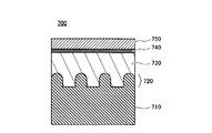
- the optical substrate of the present invention is a substrate adjacent to a semiconductor light emitting device, and is a semiconductor light emitting device composed of at least one or more n-type semiconductor layers, at least one or more p-type semiconductor layers, and one or more light emitting layers.
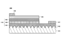
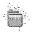
- FIG. 1 is a schematic cross-sectional view of a semiconductor light emitting element to which the optical substrate according to the present embodiment is applied.
- an n-type semiconductor layer 103, a light emitting semiconductor layer 104, and a p-type semiconductor layer 105 are sequentially stacked on an uneven structure 102 provided on one main surface of an optical substrate 101.
- a transparent conductive film 106 is formed on the p-type semiconductor layer 105.
- a cathode electrode 107 is formed on the surface of the n-type semiconductor layer 103, and an anode electrode 108 is formed on the surface of the transparent conductive film 106.
- the n-type semiconductor layer 103, the light-emitting semiconductor layer 104, and the p-type semiconductor layer 105 that are sequentially stacked on the optical substrate 101 are referred to as a stacked semiconductor layer 110.
- the semiconductor layers 103, 104, and 105 are sequentially stacked on the concavo-convex structure 102 provided on one main surface of the optical substrate 101, but the concavo-convex structure 102 of the optical substrate 101 is provided.
- a semiconductor layer may be sequentially stacked on another main surface facing the surface.
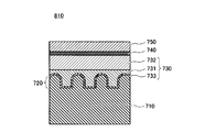
- FIG. 2 is a schematic cross-sectional view of another example of a semiconductor light emitting element to which the optical substrate according to the present embodiment is applied.
- an n-type semiconductor layer 202, a light emitting semiconductor layer 203, and a p-type semiconductor layer 204 are sequentially stacked on a substrate 201.
- a transparent conductive film 206 which is the optical substrate of this embodiment, has an uneven structure 205 on one main surface in contact with the p-type semiconductor layer 204.
- a cathode electrode 207 is formed on the surface of the n-type semiconductor layer 202, and an anode electrode 208 is formed on the surface of the transparent conductive film 206.
- the main surface on which the concavo-convex structure 205 of the transparent conductive film 206 is provided is adjacent to the p-type semiconductor layer 204, but may be provided on the main surface facing the p-type semiconductor layer 204.
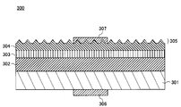
- FIG. 3 is a schematic cross-sectional view of another example of a semiconductor light emitting element to which the optical substrate according to the present embodiment is applied.
- the n-type semiconductor layer 302, the light emitting semiconductor layer 303, and the concavo-convex structure 305 provided on the main surface opposite to the light emitting semiconductor layer 303 are provided on the substrate 301.
- a p-type semiconductor layer 304 which is an optical substrate of the invention is sequentially laminated.
- a cathode electrode 306 is formed on the main surface opposite to the main surface in contact with the n-type semiconductor layer 302 of the substrate 301, and an anode electrode 307 is formed on the surface of the p-type semiconductor layer 304.
- the semiconductor light emitting devices 100, 200, and 300 shown in FIGS. 1 to 3 are examples in which the optical substrate of this embodiment is applied to a semiconductor light emitting device having a double hetero structure. It is not limited to. Further, a buffer layer (not shown) may be provided between the optical substrates 101, 201, 301 and the n-type semiconductor layer 302.
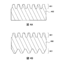
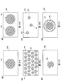
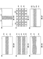
- FIG. 4A and 4B are schematic cross-sectional views of the optical substrate according to the present embodiment.
- FIG. 4A shows a case where one surface of the optical substrate 400 has a concavo-convex structure 401
- FIG. 4B the concavo-convex structure 401 may be provided on both surfaces of the optical substrate 400.
- the concavo-convex structure 401 that satisfies the scope of the present invention only needs to be formed on at least one surface of the optical substrate 400.
- the internal quantum efficiency IQE decreases due to dislocations generated by mismatch (lattice mismatch) between the lattice constant of the optical substrate and the lattice constant of the semiconductor crystal layer.
- mismatch lattice mismatch
- the crystal growth mode of the semiconductor light emitting layer can be disturbed, and the dislocations in the semiconductor crystal layer are changed to the concavo-convex structure. It can be dispersed accordingly. That is, the dislocation density can be reduced both microscopically and macroscopically. For this reason, it is possible to improve the internal quantum efficiency IQE.
- the electron injection efficiency EIE decreases due to an increase in contact resistance due to the Schottky barrier.
- An optical substrate is provided on the outermost surface of a semiconductor light emitting device having a laminated semiconductor layer constituted by laminating at least two or more semiconductor layers and a light emitting layer, so that a transparent conductive film or electrode formed on the surface thereof.
- the contact area with the pad increases according to the specific surface area of the concavo-convex structure, and the contact resistance can be reduced. For this reason, ohmic contact is improved and the electron injection efficiency EIE can be improved.
- the present inventors add a partial disturbance to the basic concavo-convex structure so that the function expressed by the original concavo-convex structure (improvement of internal quantum efficiency IQE by the fine concavo-convex structure, or electron injection efficiency). It has been found that a new optical phenomenon (light diffraction or light scattering) corresponding to the disturbance can be added to the improvement of EIE.
- the internal quantum efficiency IQE or the electron injection efficiency EIE is improved by the high-density concavo-convex structure (original function), and a new optical according to the irregularity of the concavo-convex structure (second convex part or second concave part) Since the phenomenon (light diffraction or light scattering) can be applied, the light extraction efficiency LEE can be improved while maintaining the improvement of the internal quantum efficiency IQE or the electron injection efficiency EIE.
- this principle will be described in detail including actual examination.
- Such optical scattering has a large effect of disturbing the waveguide mode. More specifically, the probability that the emitted light whose waveguide mode has been destroyed will form the waveguide mode again is greatly reduced. Therefore, the light extraction efficiency LEE can be greatly improved.
- the averaged refractive index distribution forms a distribution according to the disturbance of the concavo-convex structure. For this reason, the light behaves as if there is a medium having an effective medium approximate refractive index having an outer shape corresponding to the distribution, and therefore an optical phenomenon (light diffraction or light scattering) corresponding to the distribution. ) Can be newly expressed, and the light extraction efficiency LEE can be improved.
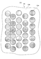
- a concavo-convex structure composed of a plurality of convex portions and concave portions arranged in a hexagonal lattice pattern having an average interval Pave of 460 nm causes light diffraction according to the average interval Pave. For this reason, as a result of visual observation, it was possible to observe glare (diffracted color) corresponding to the diffracted light (hereinafter also referred to as “original optical phenomenon”). Next, the 2nd convex part (or 2nd recessed part) was added to this uneven structure.
- the convex portions of the concavo-convex structure function as diffraction points, but when the arrangement regularity of the convex portions of the concavo-convex structure is high, the number of diffraction modes is limited by the arrangement.
- the concavo-convex structure includes the second convex portion (or the second concave portion), it is considered that the number of diffraction modes increases and dispersion is included.
- the haze for a sapphire substrate in which a plurality of convex portions with an average interval P of 300 nm are arranged in a regular hexagonal lattice pattern is a ratio of 1% in which a plurality of convex portions with an average interval P of 300 nm are arranged in a regular hexagonal lattice shape.
- the height dispersed in was 0.5 times the haze of the sapphire substrate including the second convex part with 0 nm.
- a light purple diffracted color corresponding to the average interval P was confirmed.
- the second convex portion was included, turbidity was added to the light purple diffracted color.
- the optical scattering property can be expressed by using the concavo-convex structure including the second convex portion (or the second concave portion). That is, even when a fine uneven structure is used, the waveguide mode can be disturbed by the scattering property, and the light extraction efficiency LEE can be improved.
- a concavo-convex structure composed of a plurality of convex portions and concave portions arranged in a hexagonal lattice shape having an average interval Pave of 200 nm is averaged by an effective medium approximating action.
- a transparent substrate with very little reflected light could be observed. This is generally called an antireflective film or a moth-eye structure. This is because the concavo-convex structure sufficiently smaller than the wavelength of light is averaged as viewed from the light by the effective medium approximation action.
- the concavo-convex structure includes the second convex portion (or the second concave portion), in addition to the original optical phenomenon (antireflection effect) according to the average interval Pave, the second convex portion (or It was confirmed that a scattering component corresponding to the second concave portion was further included. That is, as a result of optical measurement using light having a wavelength sufficiently larger than the average interval Pave (for example, 550 nm), it was confirmed that the scattering component becomes extremely small.
- the light used for optical measurement is considered to behave.
- the haze for the convex portions arranged in a regular hexagonal lattice pattern with an average interval Pave of 200 nm was 0.65 times the haze of the concavo-convex structure including the second convex portion with an average interval Pave of 200 nm.
- the concavo-convex structure not including the second convex portion was very transparent, but turbidity was confirmed by including the second convex portion. From the above, it can be seen that the optical scattering property can be expressed by using the concavo-convex structure including the second convex portion (or the second concave portion). That is, even with a concavo-convex structure smaller than the wavelength of light, the waveguide mode can be disturbed by the scattering property, and the light extraction efficiency LEE can be improved.
- the second convex portion (or the second concave portion) to the concavo-convex structure, it is possible to newly add a scattering property according to the second convex portion (or the second concave portion).
- the second convex portion (or the second convex portion (or the second concave portion) is included by including the second convex portion (or the second concave portion). Therefore, the light extraction efficiency LEE can be improved while maintaining the internal quantum efficiency IQE or the electron injection efficiency EIE.
- the internal quantum efficiency IQE is improved by the fine concave-convex structure, and a new optical scattering property (light diffraction or light scattering) by the second convex portion. This suggests the possibility of improving the light extraction efficiency LEE.
- a phenomenon observed when a semiconductor crystal layer is formed on the optical substrate including the second convex portion will be described.
- the leakage current of the semiconductor light emitting device is further improved when the existence probability Z of the second convex portion is not more than a predetermined value. That is, the subject of the present invention is the above-described improvement of IQE, improvement of LEE, and suppression of leakage current.
- FIG. 5 is a graph showing a relationship between the existence probability Z of the second convex portion and the leakage current in the semiconductor light emitting element to which the optical substrate according to the present embodiment is applied.
- a buffer layer, uGaN layer, nGaN layer, MQW layer, and pGaN layer were formed on the sapphire substrate (optical substrate) by MOCVD using the second projection existence probability Z as a parameter.
- ITO was formed, mesa etching was performed, and finally a metal pad pattern made of Cr / Ti / Au was formed. In this state, the leakage current was measured.
- FIG. 1 shows a graph showing a relationship between the existence probability Z of the second convex portion and the leakage current in the semiconductor light emitting element to which the optical substrate according to the present embodiment is applied.
- a buffer layer, uGaN layer, nGaN layer, MQW layer, and pGaN layer were formed on the sapphire substrate (optical substrate) by MOCVD
- FIG. 5 is a diagram showing the influence of the existence probability Z of the second convex portion on the leakage current, where the abscissa indicates the existence probability Z and the ordinate indicates the leakage current value.
- FIG. 5 shows that when the existence probability Z is small, the leakage current is further improved and good diode characteristics are exhibited. It can also be seen that the leakage current increases rapidly when the existence probability Z increases with the existence probability Z as the starting point. For example, the leakage current when the existence probability Z is 1 / 3.3 is 1.7 to 2.9 times that when the existence probability Z is 1/55. That is, it was confirmed that the diode characteristics are greatly deteriorated.
- the existence probability Z was used as a parameter and the growth property of the semiconductor crystal layer was confirmed, it was confirmed that the larger the existence probability Z, the more specific growth of the semiconductor crystal layer occurred from the vicinity of the second convex portion.
- the specific growth means that the growth rate is faster than the surroundings.
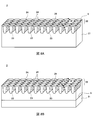
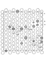
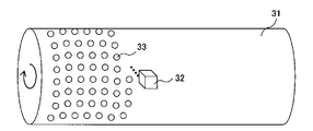
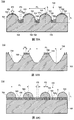
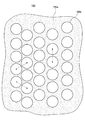
- FIG. 6 is a diagram created based on an electron micrograph of an optical substrate obtained by specifically growing a semiconductor crystal layer on the surface in order to explain the effect of the optical substrate according to the present embodiment.
- the optical substrate 600 shown in FIGS. 6A and 6B has a concavo-convex structure in which the existence probability Z is 1 / 3.3. This corresponds to the case where the existence probability Z is 0.3 in the graph shown in FIG. From FIG. 6A, it can be seen that a convex unevenness 603 occurs on the surface of the semiconductor crystal layer 602 farthest from the sapphire substrate 601 due to the specific growth.
- the unevenness 603 is caused by a semiconductor crystal layer that grows rapidly due to the formation of the second set of convex portions with a large existence probability Z.
- FIG. 6B shows that the concave unevenness 604 is generated on the surface of the semiconductor crystal layer 602 that has been specifically grown farthest from the sapphire substrate 601. This is due to the fact that the semiconductor crystal layers that have grown specifically in the second protrusions collide with each other due to the adjacent second protrusion sets caused by the large existence probability Z.
- the diode characteristics of the semiconductor light emitting device are deteriorated and the leakage current is increased. From the above, it is possible to suppress the deviation of the pn junction interface of the semiconductor crystal layer, in other words, the deviation of the band gap in the band diagram by setting the existence probability Z to be a predetermined value or less. It can be seen that can be reduced more favorably.
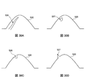
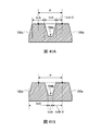
- FIG. 7A is a schematic perspective view showing the optical substrate (I) 1 according to the first embodiment.
- the optical substrate (I) 1 has a generally flat plate shape.
- the optical substrate (I) 1 includes a substrate body 11 and a concavo-convex structure 12 provided on one surface of the substrate body 11.
- the concavo-convex structure 12 includes a plurality of protrusions 13 that are independent from each other, and a continuous recess 14 provided between the protrusions 13.
- the plurality of convex portions 13 are arranged at predetermined intervals.
- the uneven structure 12 is disposed in the thickness direction of the substrate body 11.
- FIG. 8A is a schematic perspective view showing an optical substrate (II) 2 according to a second embodiment of the present invention.
- the optical substrate (II) 2 includes a substrate body 21 and a concavo-convex structure 22 provided on the surface of the substrate body 21.
- the concavo-convex structure 22 includes a plurality of concave portions 23 that are independent from each other and continuous convex portions 24 that are provided between the concave portions 23.
- the concavo-convex structure 22 includes a plurality of concave portions 23 that are disposed in the thickness direction of the substrate body 21 and are depressed.
- the plurality of recesses 23 are independent from each other and are arranged at predetermined intervals.
- the concavo-convex structure 12 is separately provided on the surfaces of the substrate bodies 11 and 21. , 22 may be provided.
- the substrate bodies 11 and 21 and the concavo-convex structures 12 and 22 are both sapphire.
- the transparent conductive film of a laminate composed of sapphire substrate / n-type semiconductor layer / light emitting layer / p-type semiconductor layer / transparent conductive film is processed, the concavo-convex structures 12 and 22 become transparent conductive films. . These are the states illustrated in FIGS. 7A and 8A.
- the concavo-convex structures 12 and 22 may be separately provided on the transparent conductive film of a laminate composed of sapphire substrate / n-type semiconductor layer / light emitting layer / p-type semiconductor layer / transparent conductive film. This is the state illustrated in FIGS. 7B and 8B.
- the material of the transparent conductive film and the concavo-convex structure may be the same or different.
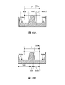
- FIG. 9 is a vertical sectional view taken along one-dot chain line III-III in FIGS. 7A and 7B and schematically shows the configuration of the concavo-convex structure 12.
- FIG. 10 is a vertical sectional view taken along the alternate long and short dash line IV-IV in FIGS. 8A and 8B and schematically shows the configuration of the concavo-convex structure 22.
- optical substrate (I) 1 First, the optical substrate (I) 1 according to the first embodiment will be described. As shown in FIG. 9, in this cross section, a plurality of convex portions 131, 132, 133, and 134 are arranged at intervals. The convex portions 131 to 134 are continuously connected by the concave portion 14.
- the symbol Scv shown in FIG. 9 indicates the convex portion average position.
- the convex portions are arranged in the thickness direction of the substrate body 11.
- the convex portion average position Scv means the in-plane average position of the convex portion vertex 13a of the convex portions 131 to 134 of the concave-convex structure 12, and is a surface parallel to the surface direction of the substrate body 11.
- the convex average position Scv is obtained according to the following definition.
- a 50 ⁇ m ⁇ 50 ⁇ m square region parallel to the main surface of the substrate body 11 is taken on the surface of the optical substrate (I) 1 on which the uneven structure 12 is formed (hereinafter referred to as an uneven structure surface).
- the 50 ⁇ m ⁇ 50 ⁇ m square region is divided into 25 by 10 ⁇ m ⁇ 10 ⁇ m square regions that do not overlap each other.
- five regions are arbitrarily selected from 25 existing 10 ⁇ m ⁇ 10 ⁇ m regions.
- the selected 10 ⁇ m ⁇ 10 ⁇ m square regions are referred to as region A, region B, region C, region D, and region E.
- region A is observed at a higher magnification, and is expanded until at least 100 convex portions 13 are clearly observed.
- ten convex portions 13 are arbitrarily selected from the observed convex portions 13 and the height of each convex portion 13 is obtained. Let the maximum height among the ten convex portions 13 measured from the region A be ha.
- region B, region C, region D, and region E the same operation as in region A is performed to obtain hb, hc, hd, and he.
- each convex part 13 is observation using the scanning electron microscope with respect to the cross section of the optical board
- the heights of the plurality of convex portions 131 to 134 are mainly the same, but are not uniform, and the second convex portions 133 having a low height are mixed in some places.
- the average convex portion position Scv of the convex portions 131 to 134 is lower than the vertex 13a of the convex portion 13 of the first convex portions 131, 132, 134. This shows a case where there is a distribution in the height of the first convex portions 131, 132, 134 from the above definition.
- the convex average position Scv is slightly smaller than the vertex 13a of the first convex portions 131, 132, and 134. It may be located above.
- the convex portion average position Scv substantially coincides with the vertex 13a of the convex portions 131, 132, and 134. Or match exactly.
- the average concave portion Scc means the average in-plane position of the concave vertex 14a of the concave portion 14 of the concave-convex structure 12, and is a surface parallel to the surface direction of the optical substrate (I) 1.
- the recesses 14 are continuous with each other, and the protrusions 131 to 134 are separated from each other by the recesses 14.
- the average recess position Scc is preferably obtained by averaging 10 recess apexes 14a.
- each concave portion 14 is obtained by observing the cross section of the optical substrate (I) 1 using a scanning electron microscope or observing the concavo-convex structure surface of the optical substrate (I) 1 using an atomic force microscope. Can be determined.
- the average in this specification means an arithmetic mean. Further, the above observation is defined to be performed within the range described below.
- a position moved by a distance corresponding to (ha + hb + hc + hd + he) / 5 toward the apex 13a of the convex portion 13 from the observed average concave portion position Scc is the convex portion average position Scv.
- a symbol lcv shown in FIG. 9 indicates a line segment on a plane formed by the convex portion average position Scv. Therefore, the line segment lcv is a surface parallel to the surface direction of the substrate body 11.
- the average convex part height Have is the distance between the convex part average position Scv and the concave part average position Scc. Therefore, the average convex height Have is (ha + hb + hc + hd + he) / 5 calculated when the convex average position Scv is obtained.
- the symbol hn shown in FIG. 9 indicates the height of the convex portions of the convex portions 131 to 134.
- the convex height hn means the distance between the center 13b of the bottom of each convex 131-134 and the vertex 13a of the convex 13 at the average concave position Scc. That is, the height hn of the protrusion corresponds to the height of the vertex 13a of each of the protrusions 131 to 134 with respect to the average concave position Scc.
- each convex portion 13 is set to Define as follows. As shown in the convex part 132, first, let X be the intersection of the line segment parallel to the thickness direction of the optical substrate (I) 1 and the contour of the convex part 132. Next, let Y be the intersection of the line segment passing through the intersection X and the average recess position Scc. When the line segment is translated in the plane direction within the concave average position Scc, the distance between the intersection X and the intersection Y changes. The maximum value of the distance between the intersection point X and the intersection point Y is hn.
- ⁇ cv The symbol ⁇ cv shown in FIG. 9 indicates the width of the bottom of the first protrusions 131, 132, 134 at the average recess position Scc.
- the bottom width ⁇ cv is defined as follows. As shown in the convex portion 134, first, an arbitrary point E on the bottom contour of the convex portion 134 is set. Next, an arbitrary point F different from the point E on the contour is set. When the point E is fixed and the point F is moved on the contour, the distance when the distance between the point E and the point F becomes the maximum is the bottom width ⁇ cv.
- each convex portion 13 is arbitrarily selected, the bottom width ⁇ cv of each convex portion 13 is obtained, and an arithmetic average of them is an average width ⁇ cv-ave of the bottom portions. Further, the above observation is defined to be performed within the range described below.
- the symbol tcv shown in FIG. 9 indicates the shortest distance between the contours between the first convex portion 132 and the first convex portion 134 that are adjacent to each other with the second convex portion 133 therebetween on the line segment lcv. That is, the symbol tcv means the distance on the line segment lcv between the first convex portions 132 and 134 adjacent to each other with the second convex portion 133 interposed therebetween.
- intersections of one first protrusion 132 and the line segment lcv are indicated by A and B in FIG. (2)
- the intersection of the first convex portion 134 adjacent to the first convex portion 132 and the second convex portion 133 between the first convex portion 132 and the line segment lcv is shown in FIG. Indicated by C and D.
- the intersections are arranged in the order of A, B, C, and D. Of these, the distance between the intersection B and the intersection C is defined as tcv. Yes.
- tcv of five points is arbitrarily measured for each second convex portion 133, and an arithmetic average value thereof, that is, an arithmetic point of 25 points is measured.
- the average value is defined as tcv-ave.
- tcv-ave is a scale that represents the size of the second convex portions to be gathered.
- tcv-ave is a distance that can be easily measured when the cross section of the optical substrate is observed with a scanning electron microscope. Further, the above observation is defined to be performed within the range described below.
- the distance tcv and the arithmetic average value tcv ⁇ ave thereof are distances described below when the convex portion average position Scv is located slightly above the vertex 13a of the first convex portions 131, 132, and 134. It is defined as Tcv or its arithmetic average value Tcv-ave.
- Tcv The symbol Tcv shown in FIG. 9 indicates the shortest distance between the vertex 13a of the first convex portion 132 and the vertex 13a of the first convex portion 134 that are adjacent to each other with the second convex portion 133 therebetween on the line segment lcv. Show. That is, the symbol Tcv means an interval on the line segment lcv between the first convex portions 132 and 134 adjacent to each other with the second convex portion 133 interposed therebetween.
- the symbol Tcv passes through the vertex 13a of the first convex portion 132 and is an optical substrate.
- Tcv of five points is arbitrarily measured for each second convex portion 133, and an arithmetic average value thereof, that is, an arithmetic average of 25 points.
- Tcv-ave is a scale representing the size of the second convex portion
- Tcv-ave is the case where the surface of the optical substrate (I) 1 is observed with a scanning electron microscope or an atomic force microscope. The distance is easy to measure. Further, the above observation is defined to be performed within the range described below.
- ⁇ P P shown in FIG. 9 is the shortest of the two first protrusions 131 and 132 adjacent to each other without the second protrusion 133 out of the plurality of first protrusions 131, 132, and 134. It is an interval.
- the average interval Pave will be described later in detail.
- the protrusion height hn is lower than the protrusions 131, 132, and 134 having substantially the same protrusion height, in other words, a protrusion with a protrusion height hn lower than the average protrusion height Have ( Hereinafter, the minimum convex portion) exists with a predetermined probability.
- the minimal convex portion is defined as the second convex portion
- the convex portion not corresponding to the minimal convex portion is defined as the first convex portion.
- a convex portion satisfying the following formula (2) with respect to the average convex portion height Have corresponding to the distance between the convex average position Scv and the concave average position Scc of the concavo-convex structure 12 is defined as a minimal convex portion. Define. Whether or not the following formula (2) is satisfied can be determined by observation with a scanning electron microscope with respect to the cross section of the optical substrate or with atomic force microscope with respect to the concavo-convex structure 12 of the optical substrate (I) 1. Further, the above observation is defined to be performed within the range described below.
- Formula (2) 0.6 Have ⁇ hn ⁇ 0
- the second convex portion is a convex portion whose height hn is lower than the average convex portion height Have. That is, the second convex portion may have a constant convex portion height, or the plurality of second convex portions may have a distribution of heights. Similarly, the height of the first protrusions may be constant or the height of the plurality of first protrusions may have a distribution.
- an optical substrate (II) 2 according to a second embodiment of the present invention shown in FIG. 8 will be described with reference to FIG.
- a plurality of recesses 231 to 234 are arranged independently of each other.
- a convex portion 24 exists between the concave portions 231 to 234, and separates the concave portions 231 to 234 from each other.
- ⁇ Scv A symbol Scv in FIG. 10 indicates the convex portion average position of the convex portion 24.
- the convex portion average position Scv means the in-plane average position of the vertex 24 a of the convex portion 24 of the convex portion 24 of the concave-convex structure 22, and is a surface parallel to the surface direction of the substrate body 21.
- the average convex portion position Scv is preferably obtained by averaging ten vertexes 24a.
- the convex average position Scv is defined as in the first embodiment. Further, the above observation is defined to be performed within the range described below.
- the symbol Scc shown in FIG. 10 indicates the average recess position of the plurality of recesses 231 to 234.
- the concave average position Scc means the average in-plane position of the vertex 23a of the concaves 231 to 234 of the concave-convex structure 22, and is a plane parallel to the surface direction of the substrate body 21.
- the average concave position Scc is determined according to the following definition. First, a 50 ⁇ m ⁇ 50 ⁇ m square region parallel to the main surface of the substrate body 21 is taken on the surface of the optical substrate (II) 2 where the concavo-convex structure 22 is formed.
- the 50 ⁇ m ⁇ 50 ⁇ m square region is divided into 25 by 10 ⁇ m ⁇ 10 ⁇ m square regions that do not overlap each other.
- five regions are arbitrarily selected from 25 existing 10 ⁇ m ⁇ 10 ⁇ m regions.
- the selected 10 ⁇ m ⁇ 10 ⁇ m square regions are referred to as region A, region B, region C, region D, and region E.
- the region A is observed at a higher magnification, and is expanded until at least 100 concave portions 23 are clearly observed.
- ten recesses are arbitrarily selected from the observed recesses 23, and the depth of each recess 23 is obtained. The maximum depth among the ten recesses 23 measured from the region A is da.
- the concave average position Scc is a position moved by a distance corresponding to (da + db + dc + dd + de) / 5 below the convex average position Scv already described, in other words, from the convex average position Scv toward the bottom of the concave 23.
- the depths of the plurality of recesses 231 to 234 are mainly the same, but are not uniform, and the second recesses 233 having a shallow depth are mixed in some places. Therefore, the average concave position Scc of the concave portions 231 to 234 is shallower than the vertex 23a of the first concave portions 231, 232, and 234. This shows a case where the height of the first recess is distributed from the above definition.
- the average recess position Scc may be positioned slightly below the vertex 23a of the first recess 231, 232, 234. .
- the recess average position Scc substantially coincides with or completely coincides with the vertex 23a of the first recesses 231, 232, 234. .
- Lcc A symbol lcc shown in FIG. 10 indicates a line segment on the plane formed by the concave average position Scc. Accordingly, the line segment lcc is parallel to the surface direction of the substrate body 21.
- the symbol Dave shown in FIG. 10 indicates the average recess depth of the recesses 231 to 234.
- the average concave portion depth Dave is a distance between the convex portion average position Scv and the concave portion average position Scc. That is, (da + db + dc + dd + de) / 5 calculated when the average concave portion position Scc is obtained.
- a symbol dn shown in FIG. 10 indicates the depth of the recesses of the plurality of recesses 231 to 234.
- the recess depth dn means the distance between the center 23b of the openings of the recesses 231 to 234 and the apex 23a of the recesses 231 to 234 at the protrusion average position Scv. That is, the recess depth dn is the depth of each of the recesses 231 to 234 with respect to the protrusion average position Scv.
- each recess 231 to 234 is set as follows: Defined in As shown in the concave portion 232, first, an intersection of a line segment parallel to the thickness direction of the optical substrate (II) 2 and the outline of a certain concave portion 232 is set to Y. Next, let X be the intersection of the line segment passing through the intersection Y and the convex portion average position Scv. When the line segment is translated in the plane direction within the convex average position Scv, the distance between the intersection X and the intersection Y changes. The maximum value of the distance between the intersection point X and the intersection point Y is dn.
- ⁇ cc The symbol ⁇ cc shown in FIG. 10 indicates the width of the opening of the first recesses 231, 232, and 234 at the protrusion average position Scv.
- the width ⁇ cc of the opening is defined as follows. As shown in the recess 234, first, an arbitrary point E on the contour of the opening of the recess 234 is set. Next, an arbitrary point F different from the point E on the contour is set. When the point E is fixed and the point F is moved on the contour, the distance when the distance between the point E and the point F becomes maximum is defined as the opening width ⁇ cc.
- the opening width ⁇ cc is obtained for each recess 23, and an arithmetic average of these is the average ⁇ cc-ave of the opening width. Further, the above observation is defined to be performed within the range described below.
- a symbol tcc shown in FIG. 10 indicates the shortest distance between the contours between the adjacent first concave portions 232 and 234 on the line segment lcc. That is, the symbol tcc means a distance on the line segment lcc of the first concave portion adjacent to the second concave portion 233.
- a line segment lcc in the plane formed by the average concave portion position Scc crosses the plurality of first concave portions 231, 232 and 234.
- the intersections of one first recess 232 and the line segment lcc are indicated by A and B in FIG.
- intersections of the first concave portion 234 adjacent to the first concave portion 232 and the second concave portion 233 between the first concave portion 232 and the line segment lcc are represented by C and D in FIG. It shows with.
- the intersections are arranged in the order of A, B, C, and D. Of these, the distance between the intersection B and the intersection C is defined as tcc. Yes.
- tcc of five points is arbitrarily measured for each second concave portion 233, and an arithmetic average value thereof, that is, an arithmetic average of 25 points.
- tcc-ave is a scale that represents the size of the second concave portion 233, and in particular, tcc-ave is easy to measure when the cross section of the optical substrate (II) 2 is observed with a scanning electron microscope. Distance. Further, the above observation is defined to be performed within the range described below. Note that the distance tcc and the arithmetic average value tcc-ave are the distance Tcc or the distance Tcc described below when the recess average position Scc is located slightly below the vertex 23a of the first recesses 231, 232, 234. It is defined as the arithmetic mean value Tcc-ave.
- Tcc The symbol Tcc shown in FIG. 10 is the shortest distance between the central portion of the opening of the first concave portion 232 and the central portion of the opening of the first concave portion 234 that are adjacent to each other with the second concave portion 233 on the line lcc. Is shown. That is, the symbol Tcc means an interval on the line segment lcv between the first concave portions 232 and 234 adjacent to each other with the second concave portion 233 interposed therebetween.
- the symbol Tcc passes through the center of the opening of the first concave portion 232 to form the optical substrate ( II)
- the intersection (M) between the line segment parallel to the thickness direction of the optical substrate (II) 2 and the line segment lcc is the shortest distance.
- Tcc means an interval in a plane parallel to the surface direction of the substrate body 21 between the central portions of the openings of the first recesses 232 and 234 adjacent to each other with the second recess 233 interposed therebetween.
- Tcc of five points is arbitrarily measured for each second concave portion 233, and an arithmetic average value thereof, that is, an arithmetic average of 25 points. Define the value as Tcc-ave.
- Tcc-ave is a scale representing the size of the second concave portion 233, and in particular, Tcc-ave is easy to measure when the surface of the optical substrate is observed with a scanning electron microscope or an atomic force microscope. It is a long distance. Further, the above observation is defined to be performed within the range described below.
- ⁇ P P shown in FIG. 10 is an interval between two adjacent ones of the plurality of first recesses 231, 232, and 234.
- the average interval Pave will be described later in detail.
- the recess depths dn of the plurality of recesses 231 to 234 are not uniform, and are almost the same as the recess 233 shown in FIG.
- the recess depth dn is shallower than the plurality of recesses 231, 232, and 234 having a depth of, that is, a recess having a recess depth dn shallower than the average recess depth d (hereinafter referred to as a minimum recess) is predetermined.
- the minimum recess is defined as the second recess, and the recess not corresponding to the minimum recess is defined as the first recess.
- a recess having a recess depth dn that satisfies the following formula (6) with respect to the average recess depth Dave corresponding to the distance between the average protrusion position Scv and the average recess position Scc of the uneven structure 22 is defined as a minimum recess.
- Whether or not the following formula (6) is satisfied can be determined by observation with a scanning electron microscope with respect to the cross section of the optical substrate (II) 2 or observation with an atomic force microscope with respect to the concavo-convex structure 22 of the optical substrate. Further, the above observation is defined to be performed within the range described below.
- the second recess 233 is the recess 23 whose depth dn is shallower than the average recess depth Dave. That is, the second concave portion 233 may have a constant concave portion depth, or a plurality of second concave portion depths may have a distribution. Similarly, the depths of the first recesses 231, 232, and 234 may be constant, or the depths of the plurality of first recesses may have a distribution.
- the plurality of first convex portions 131, 132, and 134 (concave portions 231, 232, and 234) and the first convex portions 131, 132, Second protrusions 133 (recesses 233) having a height (shallow depth) higher than 134 (recesses 231, 232, 234) are mixed.
- the second convex portion (concave portion) is the already described minimal convex portion (concave portion).
- the average interval Pave between the concavo-convex structures (I) 12 and (II) 22 is defined for the first convex portion 13 (concave portion 23).
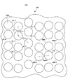
- the concavo-convex structure 12 is a structure in which a plurality of convex portions 13 are arranged unevenly and the second convex portions 51 are mixed
- the center of a certain first convex portion A1 and A distance P A1B1 between the center of the first convex portion B1 closest to the first convex portion A1 is defined as an interval P.
- the plurality of convex portions 13 are non-uniformly arranged, and when the intervals differ depending on the first convex portion to be selected, any one of the plurality of first convex portions A1, A2,.
- the plurality of convex portions 13 are non-uniformly arranged, but in a triangular lattice shape, a quadrangular lattice shape, a hexagonal lattice shape, or an array in which the number of lattice shapes of these arrays varies regularly. There may be.
- the length of the convex portion of the second convex portion 61 (the length of the second convex portion in the major axis direction) is the first It becomes below the length of the convex part.
- the interval P is equal to the center line of the certain first convex line A1 and the first convex line. It is defined as the shortest distance P A1B1 between the center line of the first convex line B1 closest to B1.
- the interval differs depending on the selected convex line, an arbitrary plurality of first convex lines A1, A2,...
- AN are selected, and each selected first convex line is selected.
- requiring the above-mentioned arithmetic mean value is 10 points
- the existence probability Z of the second convex portion or the second concave portion will be described.
- the term described above is used when the existence probability of the second convex portion or the second concave portion is obtained from actual observation. That is, the term described above is defined within a measurement range for calculating the existence probability Z of the second convex portion or the second concave portion described below.
- the concavo-convex structure is observed with a scanning electron microscope or an atomic force microscope, and the first convex portion (or the first concave portion, the same applies hereinafter) and the second convex portion (or the second concave portion, the same applies hereinafter), Carve out.
- the distinction between the first convex portion and the second convex portion is as already described.
- the concavo-convex structure surface side of the optical substrate can be directly observed
- the concavo-convex structure is observed with a scanning electron microscope or an atomic force microscope, and the second convex portion is determined.
- the semiconductor crystal layer is provided on the concavo-convex structure of the optical substrate and the semiconductor crystal layer cannot be removed, the cross section of the optical substrate is observed with a scanning electron microscope, and the second convex portion is removed. Determine.
- first convex portions are arbitrarily selected from the plurality of first convex portions, and the interval P is measured.
- the arithmetic average value of the measured intervals P of 10 points is the average interval Pave.
- interval P is the shortest space
- an area of 10 Pave ⁇ 10 Pave can be observed by observing an area of 5 Pave ⁇ 5 Pave and connecting the four.
- Tcv (or tcv) is arbitrarily measured at five points for each selected second convex portion. That is, for each selected second convex portion, Tcv (or tcv) is arbitrarily measured at five points, and thus Tcv (or tcv) measurement data is aggregated at 25 points.
- the 25-point arithmetic average value of the obtained Tcv (or tcv) is Tcv-ave (or tcv-ave).
- Tcv (or tcv) is arbitrarily set for the selected N second convex portions. 5 points are measured. That is, for each selected second convex part, Tcv (or tcv) is arbitrarily measured at five points, so that the measurement data of Tcv (or tcv) is aggregated by 5 ⁇ N points.
- the arithmetic mean value of the obtained Tcv (or tcv) is Tcv-ave (or tcv-ave).
- tcv is the shortest distance between the contours of the first convex portions adjacent to each other between the second convex portions on the line segment lcv.
- the optical substrate is observed from the cross section using a scanning electron microscope. This is useful when observing the surface using an atomic force microscope.
- Tcv is the shortest distance in the plane parallel to the surface direction of the substrate body 11 between the vertices 13a of the first protrusions 132 and 134 adjacent to each other with the second protrusion 133 interposed therebetween. Used when observing from the surface.
- a 10-fold angle area of the calculated Tcv-ave that is, 10 Tcv-ave ⁇ 10 Tcv-ave (or 10 tcv-ave ⁇ 10 tcv-ave)
- the number of first protrusions (N1) and the number of second protrusions (N2) existing in the region are counted, and the existence probability Z of the second protrusion is calculated.
- the area used to calculate Tcv-ave is always included in the area of 10 Tcv-ave ⁇ 10 Tcv-ave.
- the first and second convex portions counted within 10Tcv-ave ⁇ 10Tcv-ave are convex portions whose contours completely fit within 10Tcv-ave ⁇ 10Tcv-ave.
- the existence probability Z is given as N2 / (N1 + N2).
- (N2 / N2) / [(N1 + N2) / N2] 1 / [1+ (N1 / N2)]
- the numerator of the existence probability Z is expressed as 1 unity. ing.
- each convex portion becomes unclear, which hinders counting of the number of first convex portions and second convex portions.
- a region of 10 Tcv-ave ⁇ 10 Tcv-ave can be observed by observing a region of 5 Tcv-ave ⁇ 5 Tcv-ave and connecting the four.
- the first convex portion 71 and the second convex portion 72 are distinguished. In observation using a scanning electron microscope, information in the height direction (solid direction) cannot be obtained. Therefore, the first protrusion 71 and the second protrusion can be obtained by applying a tilt when observing. Part 72 can be discriminated. On the other hand, when observation is performed using an atomic force microscope, since the probe (probe) also detects information in the height direction (solid direction), the first convex portion 71 and the second projection are obtained from the obtained image. The convex part 72 can be distinguished. In FIG. 13, the second convex portions 72 are irregularly arranged, but the arrangement of the second convex portions 72 is not limited to this, and can be regularly arranged.
- first protrusions 71 numbered 1 to 10 in FIG. 13
- the interval P is measured for each of the selected first convex portions 71 (1 to 10) (P1 to P10 in FIG. 13).
- the arithmetic average value of the measured intervals P at 10 points, that is, (P1 + P2 +... + P10) / 10 is the average interval Pave.
- five second convex portions 72 are arbitrarily selected from the observation with respect to a region 73 that is 10 times larger than the calculated average interval Pave, that is, a region 73 for 10 Pave ⁇ 10 Pave.
- a region where the average interval Pave is measured is necessarily included in the region 73 for 10 Pave ⁇ 10 Pave.
- the second convex portions 72 to be selected are limited to those whose contours are all within the region 73 for 10 Pave ⁇ 10 Pave. That is, as shown in FIG.
- the region used to select the average interval Pave is all observed within 10 Pave ⁇ 10 Pave, and is arbitrarily selected from the second convex portion whose contour is completely within the range of 10 Pave ⁇ 10 Pave.
- Five second convex portions 72 (second convex portions 72 numbered 1 to 5 in FIG. 14) are selected.
- Tcv (or tcv) is arbitrarily measured at five points for each of the selected second convex portions 72 (1 to 5).
- Tcv (or tcv) can be measured from data obtained by observation with an atomic force microscope.
- Tcv can be measured by applying a tilt to the scanning electron microscope observation to distinguish the first convex portion 71 and the second convex portion 72 from each other.
- Tcv is measured for convenience. That is, Tcv is arbitrarily measured at five points for each of the selected second convex portions 72 (1 to 5).
- Tcv measured for the second convex portion 72 with the number 2 and the second convex portion 72 with the number 5 is shown as a representative.
- Tcv of the first convex portions 71 adjacent to each other with the selected second convex portions 72 interposed therebetween is measured.
- Tcv21 to Tcv25 are measured for the second convex portion 72 with the number 2
- Tcv51 to Tcv55 are measured for the second convex portion 72 with the number 5.
- five Tcvs are measured for each of the second convex portions 72 with numbers 1, 3, and 4. Therefore, 25 points of Tcv measurement data are tabulated.
- the arithmetic average value of the obtained Tcv 25 points is Tcv-ave.
- the area 73 for 10 Tcv-ave ⁇ 10 Tcv-ave always includes the area 73 used for calculating Tcv-ave.
- the first convex portion 71 and the second convex portion 72 counted in the region 74 for 10 Tcv-ave ⁇ 10 Tcv-ave are completely within the region 74 for 10 Tcv-ave ⁇ 10 Tcv-ave.
- FIGS. 16 and 17 are schematic views when the optical substrate according to the present embodiment is observed from the concavo-convex structure surface side.
- FIGS. 16 and 17 are simulated views of images obtained by observation using a scanning electron microscope or an atomic force microscope. Compared with the concavo-convex structure illustrated in FIGS. This is a case where there are many and a set. Even in such a case, the existence probability Z is obtained according to the definition described above.
- the first convex portion 71 and the second convex portion 72 are distinguished. In observation using a scanning electron microscope, information on the height direction (solid direction) cannot be obtained. Part 72 can be discriminated. On the other hand, when observation is performed using an atomic force microscope, since the probe (probe) also detects information in the height direction (solid direction), the first convex portion 71 and the second projection are obtained from the obtained image. The convex part 72 can be distinguished. In FIG. 16, the second convex portions 72 are irregularly arranged, but the arrangement of the second convex portions 72 is not limited to this and can be regularly arranged.
- first protrusions 71 numbered 1 to 10 in FIG. 16 are arbitrarily selected from the plurality of first protrusions 71.
- the interval P is measured for each of the selected first convex portions 71 (P1 to P10 in FIG. 16).
- the arithmetic average value of the measured intervals P at 10 points, that is, (P1 + P2 +... + P10) / 10 is the average interval Pave.
- five second convex portions are arbitrarily selected from the observation with respect to the area 73 of 10 times the calculated average interval Pave, that is, the area 73 for 10 Pave ⁇ 10 Pave.
- a region where the average interval Pave is measured is necessarily included in the region 73 for 10 Pave ⁇ 10 Pave.
- the second convex portion 72 to be selected is limited to one in which all the contours are within 10 Pave ⁇ 10 Pave. That is, as shown in FIG. 17, the region used to select the average interval Pave is all observed within 10 Pave ⁇ 10 Pave, and from the second convex portion 72 whose contour is completely within the range of 10 Pave ⁇ 10 Pave.
- Tcv or tcv is arbitrarily measured at five points for each of the selected second convex portions.
- Tcv or tcv can be measured from data obtained by atomic force microscope observation.
- Tcv can be measured by applying a tilt to the scanning electron microscope observation to distinguish the first convex portion 71 and the second convex portion 72 from each other.
- Tcv is measured for convenience. That is, Tcv is arbitrarily measured at five points for each of the selected second convex portions 72.
- Tcv measured for the second convex portion 72 with the number 3 is shown as a representative.
- Tcv of the first convex part 71 adjacent to the selected second convex part 72 is measured five by five.
- Tcv31 to Tcv35 are measured for the second convex portion 72 with the number 3.
- five Tcvs are measured for each of the second convex portions 72 with numbers 1, 2, 4, and 5. Therefore, 25 points of Tcv measurement data are tabulated.
- the arithmetic average value of the obtained Tcv 25 points is Tcv-ave.
- FIG. 18 is a schematic diagram showing regions used when the optical substrate according to the present embodiment is observed from the fine uneven surface side and the number of convex portions is counted.
- the number of first protrusions (N1) and second protrusions present in the calculated area 74 for Tcv-ave 10-fold angle that is, the area 74 for 10Tcv-ave ⁇ 10Tcv-ave.
- the number of parts (N2) is counted.
- the area 73 of 10 Tcv-ave ⁇ 10 Tcv-ave always includes the area 73 used to calculate Tcv-ave.
- the first and second protrusions counted in the region 74 for 10 Tcv-ave ⁇ 10 Tcv-ave are completely contoured in the region 74 for 10 Tcv-ave ⁇ 10 Tcv-ave. It shall fit.
- the number N1 of the first protrusions is 2944
- each convex portion becomes unclear and the number of first convex portions and second convex portions is counted. For example, as shown in FIG. 18, it is possible to observe a 5Tcv-ave ⁇ 5Tcv-ave region 76 and connect the four to observe a 10Tcv-ave ⁇ 10Tcv-ave region 74. .
- the optical scattering property (light diffraction or light scattering) is increased and the light extraction efficiency LEE is improved, and when it is 1500 nm or less, the internal quantum efficiency IQE or electron of the semiconductor light emitting device is increased. This is because the injection efficiency EIE is improved.
- the average interval Pave is 1500 nm or less, even when the existence probability Z of the second protrusions is large, the size of the second protrusions and the set of the second protrusions Since it is possible to keep the distance between each other large, the specific growth of the semiconductor crystal layer can be suppressed, and therefore, the leakage current can be kept good.
- the adjacent distance (Tcv or tcv) between the second convex portions of the first convex portions is optically increased.
- the concavo-convex structure 12 is averaged when viewed from the light, and thus the concavo-convex structure 12 functions as a thin film having an average refractive index (averaged refractive index). It will be. That is, when viewed from the light emitted from the semiconductor light emitting device, the uneven structure 12 behaves as a thin film (flat film) having an averaged refractive index in a region where the average interval Pave is as small as about 50 nm.
- the first convex portions 131, 132, and 134 and the second convex portion 133 are mixed (see FIG. 9).
- the averaged refractive index is considered to form a disturbance according to the second convex portion 133 dispersed in the first convex portions 131, 132, and 134. That is, the light emitted from the semiconductor light emitting element behaves as if there is a substance corresponding to the averaged refractive index distribution.
- the average interval Pave When the average interval Pave is 50 nm or more, the above-described adjacent distance (Tcv or tcv) becomes an appropriate size in view of the emission wavelength of the semiconductor light emitting element. That is, since the above-described averaged refractive index distribution is a distribution having an appropriate scale as viewed from the emission wavelength of the semiconductor light emitting device (a distribution larger than the average interval Pave), the emitted light is averaged. Therefore, the optical scattering property (light scattering or light diffraction) according to the refractive index distribution is increased, the number of modes for disturbing the waveguide mode is increased, and the light extraction efficiency LEE can be improved. . From the viewpoint of further exerting this effect and improving the light extraction efficiency LEE, the average interval Pave is preferably 100 nm or more, more preferably 200 nm or more, and most preferably 250 nm or more.
- the average interval Pave is 1500 nm or less, the density and specific surface area of the concavo-convex structure 12 are improved. Accordingly, dislocations inside the semiconductor crystal layer can be dispersed, and local and macroscopic dislocation density can be reduced, so that the internal quantum efficiency IQE can be increased.
- the average interval Pave is preferably 1000 nm or less, more preferably 900 nm or less, and most preferably 800 nm or less.
- the thickness of 550 nm or less is preferable because the size of the second protrusions can be reduced, and is most preferably 400 nm or less.
- the average interval Pave is preferably 1000 nm or less, more preferably 800 nm or less, and most preferably 550 nm or less.
- the dislocations in the semiconductor crystal layer are dispersed and the dislocation density is reduced, the internal quantum efficiency IQE is improved, and at the same time, the waveguide mode is set by optical scattering (light diffraction or light scattering).
- the disturbing light extraction efficiency LEE can be improved, and as a result, the external quantum efficiency EQE of the semiconductor light emitting device can be improved.
- the electron injection efficiency EIE is improved with the improvement of the ohmic contact, and at the same time, the waveguide mode is disturbed by the optical scattering property (light diffraction or light scattering) to improve the light extraction efficiency LEE.
- the external quantum efficiency EQE of the semiconductor light emitting device can be improved.
- the convex heights hn of the plurality of convex portions 131 to 134 are not uniform, and the second convexity shown in FIG.
- the convex portion height hn is lower than the first convex portions 131, 132, and 134 having substantially the same convex portion height, such as the portion (minimum convex portion) 133, in other words, the average convex portion height Have.
- a minimal convex portion 133 having a convex portion height hn is present with a predetermined existence probability Z.
- the convex height hn of the minimal convex portion 133 is an average convex portion corresponding to the distance between the convex average position Scv and the concave average position Scc of the concavo-convex structure 12.
- the existence probability Z satisfying the following formula (2) with respect to the height Have and having the minimal convex portion 133 satisfies the following formula (3).
- Formula (2) 0.6 Have ⁇ hn ⁇ 0
- Formula (3) 1/10000 ⁇ Z ⁇ 1/5
- the concavo-convex structure having a minute average interval Pave is approximated as a thin film having an averaged refractive index for the light emitted from the semiconductor light emitting device. For this reason, the critical angle corresponding to the averaged refractive index and the refractive index difference between the semiconductor crystal layers is determined, and a waveguide mode is formed.
- the averaged refractive index has a distribution. In this case, the light emitted from the semiconductor light emitting element can behave so that a substance corresponding to the averaged refractive index distribution is present there.
- the waveguide mode is disturbed by light diffraction.
- the inclusion of the minimal convex portion 133 can increase the number of modes of light diffraction and can include dispersibility in the mode. For this reason, since the waveguide mode is locally disturbed by light diffraction and is macroscopically extracted by light scattering, the light extraction efficiency LEE can be further improved.
- the presence of the minimal convex portion 133 disperses dislocations inside the semiconductor crystal layer and decreases the dislocation density, improves the internal quantum efficiency IQE, and at the same time, improves the waveguide mode by optical scattering.
- the heading light extraction efficiency LEE can be improved.
- the presence of the minimal convex portion 133 increases the specific surface area, reduces ohmic resistance, improves the electron injection efficiency EIE, and at the same time disturbs the waveguide mode due to the scattering property and improves the light extraction efficiency LEE. It becomes possible.
- the protrusion height hn of the minimum protrusion 133 preferably satisfies 0.4Have ⁇ hn from the viewpoint of more exerting optical scattering properties (light diffraction or light scattering) based on the above principle, and 0.3Have ⁇ hn is satisfied. It is more preferable to satisfy
- fill 0.1Have> hn. The most preferable state is when hn is zero. When the height hn of the minimal convex portion 133 is 0, it is difficult to distinguish between the minimal convex portion 133 and the first convex portions 131, 132, and 134.
- the average interval Pave of the first protrusions 131, 132, and 134 is used to create a range of 3 Pave ⁇ 3 Pave angles, and the first protrusions 131, 132, and 134 that are observed when the range is moved.
- the difference value at the time when the number of dots decreases is counted as the minimum convex portion 133.
- Nmax the number of first convex portions 131, 132, and 134 when the entire 3 Pave ⁇ 3 Pave is filled with the first convex portions 131, 132, and 134 is counted.
- Nmax the range of 3 Pave ⁇ 3 Pave is moved, and the number of first convex portions 131, 132, 134 is counted.
- Ndec first convex portions 131, 132, and 134 are counted within 3 Pave ⁇ 3 Pave. Further, it is assumed that N2 minimal convex portions 133 with hn> 0 are counted in the same range.
- the existence probability Z of the minimal convex portion 133 satisfying the expression (2) satisfies the expression (3), disturbances (scattering points) existing in the thin film at an averaged refractive index or a mode of light diffraction
- the number and the dispersibility are considered to increase, and the light extraction efficiency LEE based on the imparting of the scattering property can be realized.
- the existence probability Z preferably satisfies 1/3000 ⁇ Z ⁇ 1/10 and more preferably satisfies 1/1000 ⁇ Z ⁇ 1/10 from the viewpoint of imparting optical scattering properties (light diffraction or light scattering). It is preferable that 1/500 ⁇ Z ⁇ 1/10 is satisfied.
- the existence probability Z of the minimal convex portion 133 is 1/100 or less because the number of modes disturbing the waveguide mode is increased, and thus the effect of disturbing the waveguide mode is further increased. Most preferably, it is 1/60 or less. Further, if the existence probability Z is 1 / 5.5 or more, the effect of suppressing the characteristic growth of the semiconductor crystal layer is enhanced, so that the leakage current can be kept better. In this respect, the existence probability Z is more preferably 1/10 or more.
- the above-mentioned distance tcv-ave is 1.0 Pave ⁇ tcv-ave ⁇ 9. It is preferable to satisfy 5 Pave.
- the distance tcv-ave indicates the shortest distance between the contours between the first convex portion 132 and the convex portion 134 that are adjacent to each other on the line segment lcv with the minimal convex portion 133 therebetween. It shows that the size of the minimal convex portion 133 existing between the two is limited so as not to exceed the maximum value 9.5P.
- the internal quantum efficiency IQE or the electron injection efficiency EIE is simultaneously improved while maintaining the light extraction efficiency LEE based on the provision of optical scattering (light diffraction or light scattering). can do.
- the distance tcv-ave is greater than 1.0 Pave, the volume difference between the first convex portions 131, 132, and 134 and the minimal convex portion 133 is increased. For this reason, the averaged refractive index disturbance or the dispersion of the light diffraction mode becomes remarkable, and the light emitted from the semiconductor light emitting element exhibits an optical scattering property corresponding to the disturbance, and the light extraction efficiency LEE is increased. Can be improved.
- the distance tcv-ave when the distance tcv-ave is 9.5 Pave or less, the local density of dislocations generated inside the semiconductor crystal layer can be reduced, so that the internal quantum efficiency IQE can be improved. Further, since the specific surface area can be effectively increased when the distance tcv-ave is 9.5 Pave or less, the ohmic resistance is reduced and the ohmic contact is improved, so that the electron injection efficiency EIE is improved.
- the distance tcv-ave preferably satisfies 1.0 Pave ⁇ tcv-ave ⁇ 7.5 Pave from the viewpoint of further exerting this effect. Further, the distance tcv-ave is a scale representing the size of the minimal convex portions 133 to be gathered.
- the distance tcv-ave preferably satisfies 1.0 Pave ⁇ tcv-ave ⁇ 4.5 Pave, more preferably satisfies 1.0 Pave ⁇ tcv-ave ⁇ 3.0 Pave, and 1.0 Pave. Most preferably, ⁇ tcv ⁇ ave ⁇ 1.5 Pave is satisfied.
- the convex height hn of the minimal convex portion 133 satisfies 0.4 Have ⁇ hn ⁇ 0, and the existence probability Z is 1/3000 ⁇ Z ⁇ 1. / 10 and the distance tcv-ave preferably satisfies 1.0 Pave ⁇ tcv-ave ⁇ 4.5 Pave.
- the volume difference between the first convex portion 133 and the minimal convex portion 133 becomes large, and the local disorder of the averaged refractive index and the optical scattering property (light) in the minimal convex portion 133 are increased. (Diffraction or light scattering) increases, and it becomes possible to impart strong scattering properties at the nanoscale.
- the existence probability Z satisfies the above range, it becomes possible to increase the number of scattering points or the number of modes of light diffraction present in the thin film having an averaged refractive index, and the overall degree of scattering is improved.
- the light extraction efficiency LEE increases. Furthermore, since the distance tcv-ave satisfies the above range, it is possible to disperse dislocations inside the semiconductor crystal layer and reduce the local dislocation density, and to improve the internal quantum efficiency IQE by providing the nanostructure. It can be demonstrated.
- the distance tcv-ave satisfies the above range, the specific surface area is effectively increased even in the nanoscale uneven structure, so that the ohmic contact is improved and the electron injection efficiency EIE is improved. That is, the internal quantum efficiency IQE or the electron injection efficiency EIE and the light extraction efficiency LEE can be improved at the same time, and the external quantum efficiency EQE of the LED can be improved.
- the height hn of the minimal convex portion 133 satisfies 0.1 Have ⁇ hn ⁇ 0 from the viewpoint of imparting optical scattering properties (light diffraction or light scattering) at the nanoscale.
- the light extraction efficiency LEE due to the overall optical scattering property (light diffraction or light scattering) is improved by the enhanced scattering property at the nanoscale.
- high internal quantum efficiency IQE or electron injection efficiency EIE can be realized.
- the above-described distance Tcv-ave satisfies the following formula (4) with respect to the average interval Pave between the first convex portions 131, 132, and 134. It is preferable.
- Formula (4) 1.0 Pave ⁇ Tcv-ave ⁇ 11 Pave
- the distance Tcv-ave indicates the shortest distance between the vertices of the first convex portion 132 and the convex portion 134 that are adjacent to each other on the line segment lcv with the minimal convex portion 133 therebetween. Therefore, it is indicated that the size of the minimal convex portion 133 existing between the two is limited so as not to exceed the maximum value 11 Pave.
- the distance Tcv-ave is a value that does not depend on the gradient of the side surfaces of the plurality of convex portions.
- the distance Tcv-ave is larger than the distance tcv-ave.
- a value obtained by multiplying the distance tcv-ave by about 1.15 is the distance Tcv-ave. For this reason, as already described, the effect produced when the distance tcv-ave is equal to or less than 9.5 Pave is similarly expressed in the range where the distance Tcv-ave is equal to or less than 11 Pave.
- the internal quantum efficiency IQE or the electron injection efficiency EIE is maintained while maintaining the improvement of the light extraction efficiency LEE based on the provision of optical scattering (light diffraction or light scattering). It can be improved at the same time.
- the distance Tcv-ave is larger than 1.0 Pave, the volume difference between the first convex portion and the minimal convex portion 133 is increased. For this reason, the averaged refractive index disturbance or the dispersion of the light diffraction mode becomes remarkable, and the light emitted from the semiconductor light-emitting element exhibits a scattering property corresponding to the disturbance, thereby improving the light extraction efficiency LEE. be able to.
- the distance Tcv-ave when the distance Tcv-ave is 11 Pave or less, the local density of dislocations generated inside the semiconductor crystal layer can be reduced, so that the internal quantum efficiency IQE can be improved. Further, when the distance Tcv-ave is 11 Pave or less, the size of the gathering of the minimum convex portions 133 can be limited, so that the specific growth of the semiconductor crystal layer can be suppressed. For this reason, since it is possible to suppress the deviation of the band in the pn junction interface, more specifically, in the band diagram, it is possible to maintain a good leak current and improve the diode characteristics.
- the distance Tcv-ave preferably satisfies 1.0 Pave ⁇ Tcv-ave ⁇ 9.5 Pave from the viewpoint of further exerting this effect.
- the distance Tcv-ave is a scale representing the size of the minimal convex portions 133 that are gathered.
- the minimum convex part 133 gathers, the aggregate
- the distance Tcv-ave preferably satisfies 1.0 Pave ⁇ Tcv-ave ⁇ 7.5 Pave, more preferably satisfies 1.0 Pave ⁇ Tcv-ave ⁇ 5.5 Pave, and 1.0 Pave. Most preferably, ⁇ Tcv-ave ⁇ 3.5 Pave is satisfied.
- the convex height hn of the minimal convex portion 133 satisfies the following formula (9), the existence probability Z satisfies the following formula (10), and The distance Tcv-ave preferably satisfies the following formula (11).
- the convex height hn of the minimal convex portion 133 satisfies the formula (9)
- the volume difference between the first convex portions 131, 132, 134 and the minimal convex portion 133 is increased and averaged.
- the local disturbance of the refractive index and the optical scattering property (light diffraction or light scattering) at the minimal convex portion 133 become large, and it becomes possible to impart strong scattering property at the nanoscale.
- the existence probability Z satisfies the equation (10)
- the distance Tcv-ave satisfies the formula (11)
- the effect can be demonstrated. Further, when the distance Tcv-ave satisfies the equation (11), the specific surface area is effectively increased even in the nanoscale uneven structure, so that the ohmic contact is improved and the electron injection efficiency EIE is improved. That is, by simultaneously satisfying the equations (9) to (11), the internal quantum efficiency IQE or the electron injection efficiency EIE and the light extraction efficiency LEE can be improved at the same time, and the external quantum efficiency EQE of the LED can be improved. In addition, when the expressions (9) to (11) are satisfied at the same time, it is possible to increase the size at which the minimal protrusions 133 are aggregated and the dispersibility of the aggregated minimal protrusions 133.
- Formula (9) 0.4 Have ⁇ hn ⁇ 0 Formula (10) 1/3000 ⁇ Z ⁇ 1 / 7.5 Formula (11) 1.0 Pave ⁇ Tcv-ave ⁇ 7.5 Pave
- the height hn of the minimal convex portion 133 satisfies the following formula (12) from the viewpoint of imparting optical scattering properties (light diffraction or light scattering) at the nanoscale.
- the overall optical scattering property (light The light extraction efficiency LEE by diffraction or light scattering) can be improved, and a high internal quantum efficiency IQE or electron injection efficiency EIE can be realized.
- Formula (12) 0.2 Have ⁇ hn ⁇ 0
- the aspect ratio Have / ⁇ cv-ave is a ratio between the average value ⁇ cv-ave of the bottom width of the first convex portions 131, 132, and 134 of the concavo-convex structure 12 and the average value Have of the convex portion height.
- the aspect ratio Have / ⁇ cv-ave increases the volume difference between the first convex portion and the minimal convex portion 133, and the average refractive index disturbance or the optical scattering property (light diffraction or The range of 0.1 to 3.0 is preferable from the viewpoint of conferring light scattering) and imparting scattering properties while ensuring the internal quantum efficiency IQE or the electron injection efficiency EIE and improving the external quantum efficiency EQE.
- the aspect ratio Have / ⁇ cv-ave is preferably 0.5 or more and 2.5 or less, more preferably 0.5 or more and 1.5 or less. Most preferably, it is 5 or more and 1.2 or less.
- the shape of the convex portion 13 of the concavo-convex structure 12 is not limited, and the cone and the cone-shaped body having a stepped slope are provided. , Cones with convexly convex side surfaces, cones with distorted cone bottoms, cones with three or more inflection points on the cone bottom, cylinders, polygonal columns, Polygonal pyramids can be used.
- the vertex 13a of the convex portion 13 is continuously and smoothly connected, that is, the top portion of the convex portion 13 is a corner portion having a curvature radius exceeding zero. .
- the bottom of the recess 14 of the concavo-convex structure 12 has a flat surface.
- the initial growth state of the semiconductor crystal layer can be kept good, it is possible to further exhibit the effect of dislocation dispersibility due to the concavo-convex structure.
- the initial distance of the semiconductor crystal layer, particularly the nucleation can be kept good because the shortest distance between the bottom outer edges of the convex portions is 30 nm or more.
- the effect of improving the quantum efficiency IQE is increased.
- the distance is preferably 60 nm or more, because nucleation and subsequent growth become favorable, and is most preferably 80 nm or more.
- flat surface B having the bottom of the concave portion 14 of the concavo-convex structure (I) 12 and the stable growth surface of the first semiconductor layer provided on the concavo-convex structure (I) 12
- substantially parallel plane hereinafter referred to as “parallel stable growth plane”
- the substantially parallel plane are substantially parallel
- the growth mode disorder of the first semiconductor layer in the vicinity of the recess 14 of the concavo-convex structure (I) 12 is large.
- dislocations in the first semiconductor layer can be effectively reduced, so that the internal quantum efficiency IQE is improved.
- the stable growth surface refers to the surface with the slowest growth rate in the material to be grown.
- a stable growth surface appears as a facet surface during growth.
- a plane parallel to the A axis represented by the M plane is the stable growth plane.
- the stable growth surface of the GaN-based semiconductor layer is the M plane (1-100), (01-10), (-1010) of the hexagonal crystal, which is one of the planes parallel to the A axis.
- another plane including the A axis which is a plane other than the M plane of the GaN-based semiconductor, may be a stable growth plane.
- the minimal convex portions 133 may be arranged aperiodically or periodically.
- a non-periodic disturbance occurs in the averaged refractive index, and the waveguide mode is disturbed as light scattering.
- the light diffraction generated in the minimal convex portion 133 is less likely to strengthen each other, and the optical scattering property (light diffraction or light scattering) increases.
- the disturbance of the averaged refractive index becomes periodic, so that the light diffraction according to the periodicity is guided. The wave mode will be disturbed.
- the light extraction efficiency LEE can be improved by satisfying the height hn, distance Tcv-ave (or distance tcv-ave), and existence probability Z of the minimal convex portion 133 described above.
- the average interval Pave may be 1000 nm or less in order to further improve the internal quantum efficiency IQE and to maintain a good leak current. Preferably, it is 800 nm or less, more preferably 550 nm or less, and most preferably 400 nm or less.
- the average interval Pave is preferably 1000 nm or less, more preferably 800 nm or less, and more preferably 550 nm or less. Most preferred.
- the interval P is preferably 100 nm or more, more preferably 200 nm or more, and most preferably 250 nm or more.
- the recess depths dn of the plurality of recesses 231 to 234 are not uniform, and the second recess shown in FIG.
- the concave portion depth dn is shallower than the first concave portions 231, 232, 234 having substantially the same depth, in other words, the concave portion depth dn as compared with the average concave portion depth Dave.
- the concave portion depth dn is shallower than the first concave portions 231, 232, 234 having substantially the same depth, in other words, the concave portion depth dn as compared with the average concave portion depth Dave.
- the concave depth dn of the minimal concave 233 corresponds to the distance between the convex average position Scv and the concave average position Scc of the concavo-convex structure (II) 22.
- the following equation (6) is satisfied with respect to the average depth Dave of the concave portion, and the existence probability Z at which the minimal concave portion 233 exists satisfies the following equation (7).
- Formula (6) 0.6 Dave ⁇ dn ⁇ 0 Formula (7) 1/10000 ⁇ Z ⁇ 1/5
- the recess depth dn preferably satisfies 0.4 Dave ⁇ dn ⁇ 0, and preferably satisfies 0.3 Dave ⁇ dn ⁇ 0, from the viewpoint of more exhibiting optical scattering properties (light diffraction or light scattering). More preferably, it is most preferable to satisfy 0.1 Dave ⁇ dn ⁇ 0.
- the existence probability Z of the minimal concave portion 233 satisfying the expression (6) satisfies the expression (7)
- the optical scattering property is imparted for the same reason as the optical substrate (I) 1 according to the first embodiment.
- the light extraction efficiency LEE based on can be improved.
- the existence probability Z preferably satisfies 1/3000 ⁇ Z ⁇ 1/10 and satisfies 1/1000 ⁇ Z ⁇ 1/10 from the viewpoint of imparting optical scattering properties (light diffraction or light scattering). It is more preferable that 1/500 ⁇ Z ⁇ 1/10 is satisfied.
- the existence probability Z of the minimal concave portion 233 is 1/100 or less because the number of modes disturbing the waveguide mode is increased, and thus the effect of disturbing the waveguide mode is further increased. Most preferably, it is 1/60 or less. Further, if the existence probability Z is 1 / 5.5 or more, the effect of suppressing the characteristic growth of the semiconductor crystal layer is enhanced, so that the leakage current can be kept better. From this viewpoint, the probability Z is more preferably 1/10 or more.
- the optical substrate according to the first embodiment is such that the distance tcc-ave is greater than the average interval Pave of the first recesses 23. (I) For the same reason as 1, it is preferable to satisfy 1.0 Pave ⁇ tcc-ave ⁇ 9.5 Pave.
- the distance tcc-ave indicates the shortest distance between the contours between the adjacent first concave portion 232 and the concave portion 234 on the line segment lcc, and therefore, the minimal concave portion 233 existing between the two. Is limited so as not to exceed the maximum value of 9.5P.
- the optical scattering property (light diffraction or light scattering) is obtained for the same reason as the optical substrate (I) 1 according to the first embodiment.
- the internal quantum efficiency IQE or the electron injection efficiency EIE can be improved at the same time while maintaining the improvement of the light extraction efficiency LEE based on the application.
- the distance tcc-ave preferably satisfies 1.0 Pave ⁇ tcc-ave ⁇ 7.5 Pave from the viewpoint of further exerting this effect. Further, the distance tcc-ave is a measure representing the size of the gathering of the minimal concave portions 233.
- the distance tcc-ave preferably satisfies 1.0 Pave ⁇ tcc-ave ⁇ 4.5 Pave, more preferably satisfies 1.0 Pave ⁇ tcc-ave ⁇ 3.0 Pave, and 1.0 Pave. Most preferably, ⁇ tcc-ave ⁇ 1.5 Pave is satisfied.
- the recess depth dn of the minimal recess 233 satisfies 0.4 Dave ⁇ dn ⁇ 0, and the existence probability Z is 1/3000 ⁇ Z ⁇ 1 /. 10 and the distance tcc-ave preferably satisfies 1.0 Pave ⁇ tcc-ave ⁇ 4.5 Pave.
- the depth of the concave portion of the minimal concave portion 233 satisfies a predetermined range, the volume difference between the first concave portions 231, 232, 234 and the minimal concave portion 233 increases, and the refractive index averaged accordingly.
- the optical scattering property (light diffraction or light scattering) in the minimal concave portion 233 becomes remarkable. For this reason, it is possible to impart strong scattering properties at the nanoscale.
- the existence probability Z satisfies the above range
- the number of scattering points or the number of modes of light diffraction existing in the thin film having the averaged refractive index can be increased, and the degree of overall scattering is improved.
- the light extraction efficiency LEE increases.
- the distance tcc-ave satisfies the predetermined range, it is possible to disperse dislocations inside the semiconductor crystal layer and reduce the local dislocation density, and the effect of improving the internal quantum efficiency IQE by providing a nanostructure can be achieved. It can be demonstrated. That is, the internal quantum efficiency IQE or the electron injection efficiency EIE and the light extraction efficiency LEE can be improved at the same time, and the external quantum efficiency EQE of the LED can be improved.
- the recess depth dn of the minimal recess 233 satisfies 0.1 Dave ⁇ dn ⁇ 0 from the viewpoint of imparting optical scattering properties (light diffraction or light scattering) at the nanoscale.
- the light extraction efficiency LEE due to the total optical scattering (light diffraction or light scattering) is improved by the enhanced scattering property at the nanoscale.
- High internal quantum efficiency IQE or electron injection efficiency EIE can be realized.
- the above-described distance Tcc-ave satisfies the following formula (8) with respect to the average interval Pave of the first recesses.
- Formula (8) 1.0 Pave ⁇ Tcc-ave ⁇ 11 Pave
- the distance Tcc-ave indicates the shortest distance between the apexes of the first recess 232 and the recess 234 adjacent to each other between the second recesses 233 on the line segment lcc, as shown in FIG. Therefore, it is shown that the size of the minimal concave portion 233 existing between the two is limited so as not to exceed the maximum value 11 Pave.
- the distance Tcc-ave is a value that does not depend on the gradient of the side surfaces of the plurality of recesses.
- the distance Tcc-ave is larger than the distance tcc-ave.
- the distance Tcc-ave is a value obtained by multiplying the distance tcc-ave by about 1.15. For this reason, as described above, the effect produced when the distance tcc-ave is 9.5 Pave or less is similarly expressed in the range where the distance Tcc-ave is 11 Pave or less.
- the internal quantum efficiency IQE or the electron injection efficiency EIE is maintained while maintaining the improvement of the light extraction efficiency LEE based on the provision of optical scattering (light diffraction or light scattering). It can be improved at the same time.
- the distance Tcc-ave is larger than 1.0 Pave, the volume difference between the first recesses 231, 232, and 234 and the minimum recess 233 is increased. For this reason, the averaged refractive index disturbance or the dispersion of the light diffraction mode becomes remarkable, and the light emitted from the semiconductor light emitting element exhibits an optical scattering property corresponding to the disturbance, and the light extraction efficiency LEE is increased. Can be improved.
- the distance Tcc-ave when the distance Tcc-ave is 11 Pave or less, the local density of dislocations generated in the semiconductor crystal layer can be reduced, so that the internal quantum efficiency IQE can be improved.
- the distance Tcc-ave when the distance Tcc-ave is 11 Pave or less, the size of the gathering of the minimum concave portions 233 can be limited, so that the specific growth of the semiconductor crystal layer can be suppressed. For this reason, since it is possible to suppress the deviation of the band in the pn junction interface, more specifically, in the band diagram, it is possible to maintain a good leak current and improve the diode characteristics.
- the distance Tcc-ave preferably satisfies 1.0 Pave ⁇ Tcc-ave ⁇ 9.5 Pave from the viewpoint of further exerting this effect.
- the distance Tcc-ave is a scale that represents the size of the minimal recesses 233.
- the minimal concave portions 233 are gathered, a gather having a low concave portion depth is formed. In this case, optical scattering is reduced.
- the distance Tcc-ave preferably satisfies 1.0 Pave ⁇ Tcc-ave ⁇ 7.5 Pave, more preferably satisfies 1.0 Pave ⁇ Tcc-ave ⁇ 5.5 Pave, and 1.0 Pave. Most preferably, ⁇ Tcc-ave ⁇ 3.5 Pave is satisfied.
- the recess depth dn of the minimal recess 233 satisfies the following formula (13), the existence probability Z satisfies the following formula (14), and the distance It is preferable that Tcc-ave satisfies the following formula (15).
- the recess height dn of the minimum recess 233 satisfies the formula (13)
- the volume difference between the first recesses 231, 232, 234 and the minimum recess 233 increases, and the average refractive index
- the local disturbance and the optical scattering property (light diffraction or light scattering) in the minimal concave portion 233 are increased, and it becomes possible to impart strong scattering property at the nanoscale.
- the existence probability Z satisfies the equation (14)
- the distance Tcc-ave satisfies the equation (15)
- the specific surface area is effectively increased even in the nanoscale uneven structure, so that the ohmic contact is improved and the electron injection efficiency EIE is improved. That is, by simultaneously satisfying the equations (13) to (15), the internal quantum efficiency IQE or the electron injection efficiency EIE and the light extraction efficiency LEE can be improved at the same time, and the external quantum efficiency EQE of the LED can be improved.
- the expressions (13) to (15) are satisfied at the same time, the size of the gathering of the minimal recesses 233 and the dispersibility of the gathered minimal recesses 233 can be improved. Therefore, crevasse-like defects generated in the semiconductor crystal layer can be suppressed.
- the depth dn of the minimal concave portion 233 satisfies the following formula (16) from the viewpoint of imparting optical scattering properties (light diffraction or light scattering) at the nanoscale.
- the overall optical scattering property (light The light extraction efficiency LEE by diffraction or light scattering) can be improved, and a high internal quantum efficiency IQE or electron injection efficiency EIE can be realized.
- Formula (16) 0.2 Dave ⁇ dn ⁇ 0
- the aspect ratio Dave / ⁇ cc-ave of the first recesses 231, 232, 234 is determined by the average width ⁇ cc-ave of the openings of the first recesses 231, 232, 234 of the concavo-convex structure (II) 22 and the average depth of the recesses. It is a ratio to Dave.
- the aspect ratio Dave / ⁇ cc-ave is preferably in the range of 0.1 to 3.0 for the same reason as the optical substrate (I) 1 according to the first embodiment.
- the aspect ratio Dave / ⁇ cc-ave is preferably 0.5 or more and 2.5 or less, more preferably 0.5 or more and 1.5 or less, Most preferably 0.5 or more and 1.2 or less
- the shape of the concave portion 23 of the concavo-convex structure (II) 22 is not limited.
- a cone, a cone whose side surface is bulging upward, a cone whose bottom surface is distorted, a cone whose outer shape has three or more inflection points, a cylinder, many A prism, polygonal pyramid, etc. can be adopted.
- the concavo-convex structure (II) 22 having a flat surface at the top of the convex portion 24 and the curvature radius of the vertex of the concave portion 23 being greater than 0, the vertex of the convex portion 24 It is preferable that 24a is connected continuously and smoothly and is any one of the concavo-convex structure (II) 22 having a flat surface at the bottom of the recess 23.
- the side surface of the recess may be smooth, or another unevenness may be provided on the side surface of the recess.
- the bottom part of the recessed part 23 has a flat surface.
- the diameter of the circle is 30 nm or more, so that the initial growth property of the semiconductor crystal layer can be kept good. Therefore, the effect of improving the internal quantum efficiency IQE is increased.
- the diameter is more preferably 60 nm or more, and most preferably 80 nm or more.
- the surface substantially parallel to the stable growth surface of the first semiconductor layer hereinafter referred to as “parallel stable growth surface”
- parallel stable growth surface the surface substantially parallel to the stable growth surface of the first semiconductor layer
- the first semiconductor layer near the recess 23 of the concavo-convex structure (II) 22 Since the disorder of the growth mode of the semiconductor layer is increased and the dislocations in the first semiconductor layer can be effectively reduced, the internal quantum efficiency IQE is improved.
- the stable growth surface refers to the surface with the slowest growth rate in the material to be grown. In general, it is known that a stable growth surface appears as a facet surface during growth.
- a plane parallel to the A axis represented by the M plane is the stable growth plane.
- the stable growth surface of the GaN-based semiconductor layer is the M plane (1-100), (01-10), (-1010) of the hexagonal crystal, which is one of the planes parallel to the A axis.
- another plane including the A axis which is a plane other than the M plane of the GaN-based semiconductor, may be a stable growth plane.
- the minimal concave portion 233 may be disposed aperiodically or periodically.
- one of the surfaces of the optical substrates (I) 1 and (II) 2 is used.
- the concavo-convex structures (I) 12 and (II) 22 described above are arranged on the part or the entire surface.
- a part or the whole is as follows.
- the optical substrates (I) 1 and (II) 2 according to the above-described embodiment include the uneven structure according to the present embodiment described above on a part or the entire surface of the optical substrate. That is, even if the entire surface of the optical substrate is covered with the uneven structure described above, the uneven structure described above may be provided on a part of the surface of the optical substrate.
- the concavo-convex structure described above is referred to as a concavo-convex structure G
- a concavo-convex structure that does not correspond to the concavo-convex structure described above is referred to as a concavo-convex structure B.
- the optical substrates (I) 1 and (II) 2 have a concavo-convex structure G at least partially. That is, the entire surface of the optical substrate may be covered with the concavo-convex structure G, or a part thereof may be covered.
- a region that is not covered by the uneven structure G is referred to as a “non-G region”.
- the non-G region is constituted by the concavo-convex structure B and / or a flat portion. Even in the case where a non-G region is provided on a part of the surface of the optical substrate, the already described effect can be exhibited in the region covered with the concavo-convex structure G. Therefore, the internal quantum efficiency IQE and the light extraction efficiency LEE At the same time, the leakage current can be suppressed.
- the concavo-convex structure G provided on the surface of the optical substrate is provided at least in a region having an area of 10 Pave ⁇ 10 Pave when the average interval Pave is used, because the above-described effects are exhibited. That is, for example, when the surface of the optical substrate is observed using a scanning electron microscope, the region having an area of 10 Pave ⁇ 10 Pave only needs to be configured by the concavo-convex structure G. In particular, it is preferable that the ratio or size of the concavo-convex structure G described below is satisfied by the total sum of the concavo-convex structure G that fills a region having an area of 10 Pave ⁇ 10 Pave.
- the inside of the range having an area of 10 Pave ⁇ 10 Pave is constituted by the concavo-convex structure G, and a plurality of such ranges can be provided.
- the ratio or the size of the concavo-convex structure G described below is satisfied by the sum of the concavo-convex structures G.
- the region having an area of 50 Pave ⁇ 50 Pave or more, more preferably 75 Pave ⁇ 7 Pave P or more is constituted by the concavo-convex structure G, so that the internal quantum efficiency in the non-G region adjacent to the region covered with the concavo-convex structure G It is preferable because IQE and light extraction efficiency LEE are also improved. This effect is more exhibited as it becomes 100 Pave ⁇ 100 Pave or more, 150 Pave ⁇ 150 Pave or more, and 450 Pave ⁇ 450 Pave or more. Also in these cases, it is preferable that the ratio or the size of the concavo-convex structure G described below is satisfied by the total sum of the concavo-convex structure G.
- the ratio of the non-G region is preferably 1/5 or less of the concavo-convex structure G.
- the effect of the uneven structure G can be exhibited.
- it is more preferably 1/10 or less, more preferably 1/25 or less, and most preferably 1/50 or less.
- the improvement effect of internal quantum efficiency IQE can be improved more by satisfying 1/100 or less. In particular, it is preferable to satisfy 1/500 or less, more preferably 1/1000 or less, since the uniformity of emitted light emitted from the semiconductor light emitting element is improved.
- the lower limit value is not particularly limited, and it is preferable that the lower limit value is smaller, in other words, the closer to 0, the more remarkable the effect of the concavo-convex structure G becomes.
- the ratio of the concavo-convex structure G to the surface of the optical substrate depends on the outer shape and size of the semiconductor light-emitting element, but if it is 0.002% or more, the effects already described in the concavo-convex structure G can be obtained. This is preferable because it becomes possible.
- the optical substrate has the concavo-convex structure G of 0.02% or more, more preferably 0.2% or more, dispersibility of dislocations in the semiconductor crystal layer is improved, so that the internal quantum efficiency IQE is uniform. Improves. Further, since the optical scattering points are dispersed, the uniformity of the light extraction efficiency LEE is improved.
- the internal quantum efficiency IQE and the light extraction efficiency LEE in the non-G region are preferably increased.
- the optical substrate contains the concavo-convex structure G of 2.3% or more, more preferably 10% or more, the above effect can be further exhibited.
- the ratio is 20% or more, the in-plane uniformity of the semiconductor crystal layer formed on the optical substrate is improved, so that a semiconductor light emitting device in which the internal quantum efficiency IQE and the light extraction efficiency LEE are simultaneously improved is obtained.
- the yield is improved.
- the concavo-convex structure G is preferably included by 30% or more, more preferably 40% or more, and most preferably 50% or more.
- the concavo-convex structure G when included 60% or more, the propagation of the effect of the concavo-convex structure G to the non-G region is improved. That is, since the semiconductor crystal layer in which dislocations are reduced by the concavo-convex structure G propagates to the non-G region, the degree of improvement in the internal quantum efficiency IQE of the non-G region is also increased. On the other hand, since the degree of dispersion at the interface between the concavo-convex structure G and the non-G region is increased, the optical scattering property at the interface is enhanced. Therefore, the light extraction efficiency LEE in the non-G region is also improved.
- the uneven structure G is preferably included by 70% or more, more preferably 80% or more, and most preferably 90% or more.
- the concavo-convex structure G is included 100%, in other words, when the surface of the optical substrate is completely filled with the concavo-convex structure G, the growth of the semiconductor crystal layer is uniform in the plane of the optical substrate.
- the equalization of the improvement degree of quantum efficiency IQE and light extraction efficiency LEE is promoted. That is, the performance distribution curve of the semiconductor light emitting device becomes sharper.
- the concavo-convex structure G included in the surface of the optical substrate is preferably 0.0025 ⁇ 10 ⁇ 6 m 2 or more.
- the light emission output when viewed as an LED chip is increased. Although this depends on the size and outer shape of the LED chip, it can be determined from the collision probability between the emitted light guided in the LED chip and the concavo-convex structure G.
- filling this range the initial stage growth property of the semiconductor crystal layer formed into a film on the uneven structure G becomes favorable.
- the concavo-convex structure G included on the surface of the optical substrate is preferably 0.01 ⁇ 10 ⁇ 6 m 2 or more, and preferably 0.04 ⁇ 10 ⁇ 6 m 2 or more. Is more preferable, and 0.09 ⁇ 10 ⁇ 6 m 2 or more is most preferable.
- the in-plane uniformity of the semiconductor crystal layer formed on the optical substrate is improved by being 0.9 ⁇ 10 ⁇ 6 m 2 or more, the internal quantum efficiency IQE and the light extraction efficiency LEE, At the same time, the yield of obtaining a semiconductor light emitting device improved is improved.
- the propagation of the effect of the uneven structure G to the non-G region is improved.
- the degree of improvement in the internal quantum efficiency IQE of the non-G region is also increased.
- the degree of dispersion at the interface between the concavo-convex structure G and the non-G region is increased, the optical scattering property at the interface is enhanced. Therefore, the light extraction efficiency LEE in the non-G region is also improved.
- it is not less than 3.6 ⁇ 10 ⁇ 3 m 2 , more preferably not less than 7.5 ⁇ 10 ⁇ 3 m 2 , so that a good LED can be obtained even when the outer edge portion of the LED substrate is used. Can be obtained.
- At least one concavo-convex structure G that satisfies the size of the concavo-convex structure G described above on the surface of the optical substrate it is possible to obtain an LED substrate capable of manufacturing a highly efficient LED.
- a plurality of concavo-convex structures G that satisfy the size of the concavo-convex structure G described above can also be provided.
- at least one uneven structure G satisfies the above size.
- the arrangement relationship between the concavo-convex structure G and the non-G region is not particularly limited as long as the above contents are satisfied.
- the arrangement relationship between the concavo-convex structure G and the non-G region can include the arrangement described below when the concavo-convex structure G and the non-G region are considered.
- the concavo-convex structure G is a set of concavo-convex structures G that satisfies one or more of ⁇ , ⁇ , ⁇ , and ⁇ described above, that is, a concavo-convex structure G region.
- ⁇ , ⁇ , ⁇ , and ⁇ described above
- FIG. 19 is an explanatory diagram showing the relationship between the concavo-convex structure G and the non-G region in the optical substrate according to the present embodiment.
- 19A and 19B a plurality of non-G regions 502 whose contours are indefinite are arranged in the concavo-convex structure G region 501.
- FIG. 19C a lattice-like non-G region 502 is provided in the concavo-convex structure G region 501.
- FIG. 19D a plurality of substantially circular non-G regions 502 are formed in the concavo-convex structure G region 501.
- the contour shape formed by the concavo-convex structure G region 501 is not particularly limited. That is, the interface shape between the concavo-convex structure G region 501 and the non-G region 502 is not limited. For this reason, for example, the interface shape between the concavo-convex structure G region 501 and the non-G region 502 includes an n-gon (n ⁇ 3), a non-n-gon (n ⁇ 3), a lattice shape, a line shape, and the like.
- the n-gon may be a regular n-gon or a non-regular n-gon.
- FIG. 20 is a schematic diagram showing a contour shape formed by the concavo-convex structure G region in the optical substrate according to the present embodiment.
- a quadrangular shape a regular quadrangular shape (square), a rectangular shape, a parallelogram shape, a trapezoid shape, and a shape in which one or more sets of opposing sides of these quadrangular shapes are non-parallel are exemplified.
- n-gon n ⁇ 3
- FIGS. 20A to 20D are included.
- 20A is a quadrangle
- FIG. 20B is a hexagon
- FIG. 20C is an octagon
- FIG. 20D is a dodecagon.
- the non-n-gonal shape has a structure including a corner portion with a radius of curvature exceeding 0, for example, a circle, an ellipse, or a shape with rounded corners of the n-angle described above (the radius of curvature of the corner of the n-angle above 0 Shape) or the above-described n-gon (n ⁇ 3) including a rounded corner (a portion having a radius of curvature exceeding 0).
- the shapes illustrated in FIGS. 20E to 20H are included. Note that as the contour shape of the non-G region, the shape described as the contour shape of the set of the concavo-convex structure G described above can be adopted.
- FIG. 21 is a schematic plan view showing a state where the optical substrate according to the present embodiment is observed from the surface.
- 21A to 21F show a state in which the concavo-convex structure G region 501 is surrounded by the non-G region 502.
- FIG. 21A a concavo-convex structure G region 501 may be provided on the surface of the optical substrate 500, and the outer side may be configured by a non-G region 502.
- This uneven structure G region 501 preferably satisfies the above-described ratio.
- region 501 satisfy
- a plurality of concavo-convex structure G regions 501 are arranged apart from each other on the surface of the optical substrate, and the concavo-convex structure G regions 501 and between the concavo-convex structure G regions 501 are non-G. It may be filled with region 502. In this case, it is preferable to satisfy the above-described ratio with respect to the total area of the uneven structure G.
- the uneven structure G regions 501 may be regularly arranged as shown in FIG. 21C or irregularly arranged as shown in FIG. 21D. Examples of the regular arrangement include a tetragonal arrangement, a hexagonal arrangement, an arrangement in which these arrangements are extended in a uniaxial direction, and an arrangement in which these arrangements are extended in a biaxial direction. Furthermore, although the contour shape of the concavo-convex structure G region 501 is described as a circle in FIGS.
- an irregular shape can be adopted as shown in FIG. 21E.
- examples of the outer shape of the concavo-convex structure G region 501 include shapes such as an n-gon (n ⁇ 3), a rounded-angle n-gon (n ⁇ 3), a circle, an ellipse, a line, a star, and a lattice. it can.
- the concavo-convex structure G region 501 can be surrounded by the non-G region 502
- the outer periphery thereof can be surrounded by the concavo-convex structure G region 501 and the outer periphery can be surrounded by the non-G region 502.
- the concavo-convex structure G region 501 is described in a circular shape, but the shape described with reference to FIG. 20 can be adopted as the contour shape formed by the concavo-convex structure G region 501.
- FIG. 22 is a schematic plan view showing a state where the optical substrate according to the present embodiment is observed from the surface.
- FIG. 22 shows a case where the concavo-convex structure G region 501 is sandwiched between non-G regions 502.
- a concavo-convex structure G region 501 may be provided on the surface of the optical substrate 500, and the outer side may be configured by a non-G region 502.
- This uneven structure G preferably satisfies the above-described ratio. Moreover, it is preferable to satisfy the size already described. As shown in FIG.
- a plurality of concavo-convex structure G regions 501 are arranged on the surface of the optical substrate 500 so as to be separated from each other, and the concavo-convex structure G regions 501 and the outside of the concavo-convex structure G region 501 are non-G regions 502. May be satisfied.
- it is preferable that at least one concavo-convex structure G satisfies the size already described, and it is more preferable that all the concavo-convex structures G satisfy the size already described. Further, as shown in FIG.
- an arrangement may be made in which the concavo-convex structure G region 501 is continuously provided so as to include the non-G region 502.
- the uneven structure G satisfies the size already described.
- the interface shape between the concavo-convex structure G region 501 and the non-G region 502 may be linear, or may be bent as shown in FIG. 22E.
- Examples of the shape of the concavo-convex structure G region 501 include a line shape, a lattice shape, and a mesh shape.
- FIG. 22D an arrangement may be made in which the concavo-convex structure G region 501 is continuously provided so as to include the non-G region 502.
- the concavo-convex structure G region 501 can be sandwiched between the non-G regions 502, the outer periphery thereof can be sandwiched by the concavo-convex structure G region 501 and the outer periphery can be sandwiched by the non-G region 502.
- the contour line formed by the concavo-convex structure G region 501 is described in a linear shape or a substantially linear shape, but the shape described with reference to FIG. 20 can be employed.
- the interface shape between each concavo-convex structure G region 501 and non-G region 502 is different for each concavo-convex structure G region 501 even if it is single. May be.
- the concavo-convex structure G region 501 is surrounded by the non-G region 502 and the concavo-convex structure G region 501 is sandwiched between the non-G regions 502. Can be mixed.
- a non-G region 502 is provided outside the first concavo-convex structure G region 501 (G1), and a second concavo-convex structure G region 501 (G2) is further provided outside the non-G region 502.
- the second uneven structure G region 501 (G2) may be discontinuous.
- the non-G region may be composed of the concavo-convex structure B, may be composed of a flat portion, or may be composed of the concavo-convex structure B and a flat portion.
- the uneven structure G may be the uneven structure (I) 12 according to the first embodiment and the uneven structure (II) 22 according to the second embodiment.
- the concavo-convex structure B may be the concavo-convex structure (III) according to the third embodiment described below or / and the concavo-convex structure (IV) according to the fourth embodiment.
- the outer shape of the optical substrate 500 is drawn as a rectangle.
- the outer shape of the optical substrate 500 is not limited to this.
- n ⁇ 3 non-n-gonal shape (n ⁇ 3), lattice shape, line shape, and the like can be adopted.
- the n-gon may be a regular n-gon or a non-regular n-gon.
- a quadrangular shape square
- a rectangular shape a parallelogram shape
- a trapezoid shape and a shape in which one or more sets of opposing sides of these quadrangular shapes are non-parallel are exemplified.
- n-gon when n is 4 or more, shapes as shown in FIGS. 20A to 20D are included.
- 20A is a quadrangle
- FIG. 20B is a hexagon
- FIG. 20C is an octagon
- FIG. 20D is a dodecagon.
- a non-n-gonal shape is a structure without a corner, for example, a circle, an ellipse, a shape with rounded corners of the above-described n-gonal shape (a shape with a curvature radius of n-cornered corners exceeding 0), or a rounded shape.
- n-gon (n ⁇ 3) including a corner (a corner having a radius of curvature greater than 0).
- the shapes illustrated in FIGS. 20F to 20H are included. Among these, it is preferable to adopt a line-symmetric shape.
- the substrate body 11 and the concavo-convex structure (I) 12 may be made of the same material or different materials. Further, the substrate body 11 may be directly processed to provide the uneven structure (I) 12, or a layer of the uneven structure (I) 12 may be separately provided on the substrate body 11.
- a method of forming a predetermined layer on the substrate body 11 and directly processing the formed layer, or on the substrate body 11 A method of separately growing a layer so as to form the concavo-convex structure (I) 12 and a method of imparting the concavo-convex structure (I) 12 by transfer so as to form the concavo-convex structure (I) 12 on the substrate body 11 are adopted. Can do.
- an electron beam drawing method EB method
- a photolithography method using a photosensitive resist a thermal lithography method using a heat-sensitive resist
- an interference exposure method a nanoimprint lithography method
- processing using a mask prepared by self-organization processing using nano-particles as a mask
- residual film processing using a mold having a concavo-convex structure including a mask layer inside a concave portion of the concavo-convex structure on the surface Nanoimprint lithography which does not need to be mentioned.
- a nanoimprint method for example, a nanoimprint method, a macro layer separation method, a micro layer separation method, an alternating lamination method, fine particles, fine particles, and organic substances
- a method of applying the mixture spin coating method, dip coating method, etc.
- metal, metal oxide, AlN, spin-on-carbon, spin-on-glass, SiC, etc. are deposited by vacuum film-forming methods (evaporation method, sputtering method, MOCVD method, etc.) or wet methods (cast method, spin-coating method, etc.).
- Electron beam drawing method for the deposited layer, photolithography method using a photosensitive resist, thermal lithography method using a thermosensitive resist, nanoimprint lithography method, and mask layer inside the concave portion of the concavo-convex structure
- EB method Electron beam drawing method
- a method of applying a nanoimprint lithography method that does not require a residual film treatment using a mold having a concavo-convex structure enclosing a surface on the surface may be used.
- a vacuum film forming method evaporation method, sputtering method, MOCVD method, etc.
- a wet method a method in which a metal, metal oxide, AlN, spin-on-carbon, spin-on-glass, SiC, or the like is embedded in the recess and then the resin layer is lifted off may be used.
- the material of the substrate body is not particularly limited as long as it can be used as a substrate for a semiconductor light emitting device.
- a substrate such as lithium aluminum oxide, neodymium gallium oxide, lanthanum strontium aluminum tantalum, strontium titanium oxide, titanium oxide, hafnium, tungsten, molybdenum, GaP, or GaAs can be used.
- a crystal plane suitable for the semiconductor light emitting element can be appropriately selected as the crystal plane of the substrate body 11.
- a c-plane, an m-plane, a crystal plane represented by an a-plane, and those with an off-angle can be adopted.
- the material of the p-type semiconductor layer can be used as a p-type semiconductor layer suitable for LED.
- elemental semiconductors such as silicon and germanium
- compound semiconductors such as III-V, II-VI, and VI-VI can be appropriately doped with various elements.
- the material of the transparent conductive film is not particularly limited as long as it can be used as a transparent conductive film suitable for LEDs.
- a metal thin film such as a Ni / Au electrode or a conductive oxide film such as ITO, ZnO, In 2 O 3 , SnO 2 , IZO, or IGZO can be applied.
- ITO is preferable from the viewpoints of transparency and conductivity.
- the concavo-convex structure (I) 12 and the concavo-convex structure (I) 12 when the layers of the concavo-convex structure (I) 12 concavo-convex structure (I) 12 and (II) 22 are separately formed.
- the material of (II) 22 is not particularly limited as long as it can be used as a semiconductor light emitting device.
- inorganic fine particles metal fine particles, metal oxide fine particles
- inorganic fillers metal alkoxides, metal alkoxides typified by silane coupling materials, AlN, SiC, spin-on-glass, spin-on-carbon, GaN, nitride semiconductor, AlN, GaAsP, GaP, AlGaAs, InGaN, GaN, AlGaN, ZnSe, AlHaInP, or the like can be used.
- a more preferable state as a semiconductor light emitting device is that the substrate bodies 11 and 21 and the concavo-convex structures (I) 12 and (II) 22 are the same material, and the substrate bodies 11 and 21 are sapphire, SiC, or a nitride semiconductor.
- the substrate bodies 11 and 21 are sapphire, SiC, or a nitride semiconductor, and the concavo-convex structures (I) 12 and (II) 22 are nitride semiconductors.
- the semiconductor light emitting device includes at least one or more of the optical substrate (I) 1 and the optical substrate (II) 2 according to the above-described embodiment.
- the optical substrate according to the present embodiment it is possible to improve internal quantum efficiency IQE, electron injection efficiency EIE, and light extraction efficiency LEE. Furthermore, leakage current can be suppressed.
- the semiconductor light emitting element has, for example, a laminated semiconductor layer configured by laminating at least two semiconductor layers and a light emitting layer on the main surface of the substrate.
- the laminated semiconductor layer includes a concavo-convex structure layer including dots composed of a plurality of convex portions or concave portions extending in the out-of-plane direction from the outermost surface semiconductor layer main surface, and the concavo-convex structure layer includes the above-described embodiment. This corresponds to the concavo-convex structure of the optical substrate (I) 1 and the optical substrate (II) 1.
- the stacked semiconductor layer is as described with reference to FIGS.
- the n-type semiconductor layer is not particularly limited as long as it can be used as an n-type semiconductor layer suitable for an LED.
- elemental semiconductors such as silicon and germanium, compound semiconductors such as III-V group, II-VI group, VI-VI group, and the like can be appropriately doped with various elements.
- an n-type cladding layer and a p-type cladding layer (not shown) can be appropriately provided in the n-type semiconductor layer and the p-type semiconductor layer.
- the light emitting semiconductor layer is not particularly limited as long as it has a light emitting characteristic as an LED.
- a semiconductor layer such as AsP, GaP, AlGaAs, InGaN, GaN, AlGaN, ZnSe, AlHaInP, or ZnO can be used as the light emitting semiconductor layer.
- the light emitting semiconductor layer may be appropriately doped with various elements according to characteristics.
- a low-temperature growth buffer layer for example, Al x Ga 1-x N
- an undoped semiconductor layer for example, undoped GaN
- the n-type semiconductor layer used in the above description includes a low-temperature growth buffer layer and an undoped semiconductor layer.
- These laminated semiconductor layers can be formed on the surface of the optical substrate by a known technique.
- a metal organic chemical vapor deposition method MOCVD
- HVPE hydride vapor phase epitaxy method
- MBE molecular beam epitaxy method
- the semiconductor light emitting device has the structure described with reference to FIGS. 1 to 3 as a basic structure, and can further provide a concavo-convex structure at the interface that suppresses total reflection.
- the uneven structure provided separately is not limited as long as it does not negatively affect the internal quantum efficiency IQE, light extraction efficiency LEE, and electron injection efficiency EIE of the semiconductor light emitting device.
- the average interval of the uneven structure provided separately is preferably 50 times or more the emission wavelength of the semiconductor light emitting element. In this case, light scattering can be used as an optical phenomenon.
- the average interval of the uneven structure provided separately is 0.8 times or more and less than 50 times the emission wavelength of the semiconductor light emitting element.
- optical diffraction can be used as an optical phenomenon.
- the average interval between the separately provided uneven structures is preferably 0.8 times or less the emission wavelength of the semiconductor light emitting element. In this case, in order to further improve the light extraction efficiency, it is preferable to satisfy the concavo-convex structure according to the present invention.
- optical substrate (I) 1 Next, a method for manufacturing the optical substrate (I) 1 according to the first embodiment will be described.
- the manufacturing method shown below is an example, Comprising: The manufacturing method of optical board
- FIG. 23 is a schematic diagram showing an example of a manufacturing method of the optical substrate (I) 1.
- the cylindrical mold 31 having a thermally reactive resist (resist layer) uniformly formed on the surface is prepared.
- the surface of the cylindrical mold 31 is scanned in the direction of the cylinder axis of the cylindrical mold 31 while irradiating the surface of the cylindrical mold 31 with a pulse laser from the laser irradiation unit 32.
- patterns 33 are recorded at arbitrary intervals on the resist layer on the outer peripheral surface of the cylindrical mold 31 in the rotational direction.
- an operation that does not irradiate y pulses after irradiating x pulses is set as one period, or y pulses are irradiated with power r after irradiating x pulses with power q.
- the optical substrate (I) 1.
- the existence probability Z of the minimal recess 233 can be set arbitrarily. Since the pulse laser scans in the cylindrical axis direction of the cylindrical mold 31, when the cylindrical mold 31 makes one round from an arbitrary position, the laser irradiation unit 32 is shifted in the cylindrical axis direction.
- the method for transferring the pattern 33 obtained as described above to the substrate body 11 is not particularly limited, and for example, a nanoimprint lithography method can be used.
- this nanoimprint lithography method is performed, the residual film treatment can be made unnecessary by using a mold having a concavo-convex structure including a mask layer inside a concave portion of the concavo-convex structure on the surface.
- the pattern 33 (uneven structure) is transferred to a film from the cylindrical mold 31 having the pattern 33 obtained as described above, and a resin mold is manufactured. Then, by using the obtained resin mold as a mold and processing the substrate body 11 by the nanoimprint lithography method, the optical substrate (I) 1 can be manufactured. According to this method, the utilization efficiency of the mold can be increased and the flatness of the substrate body 11 can be absorbed.
- the method for transferring the pattern 33 from the cylindrical mold 31 to the resin mold is not particularly limited, and for example, a direct nanoimprint method can be applied.
- Examples of the direct nanoimprint method include a thermal nanoimprint method and an optical nanoimprint method.
- the cylindrical mold 31 is filled with a thermosetting resin while being heated at a predetermined temperature, the cylindrical mold 31 is cooled, and then the cured thermosetting resin is released to form a film.
- a reel-shaped resin mold can be obtained.
- the photocurable resin filled in the cylindrical mold 31 is irradiated with light of a predetermined wavelength to cure the photocurable resin, and then the photocurable resin cured from the cylindrical mold 31. By releasing the mold, a film-shaped or reel-shaped resin mold can be obtained.
- the resin mold method is preferable because repeated transfer is easy.
- “repeated transfer” means (1) producing a plurality of transferred concavo-convex pattern transfer products from a resin mold (+) having a concavo-convex pattern shape, or (2) a curable resin composition in particular.
- a reversed transfer body ( ⁇ ) is obtained from the resin mold (+), and then a reverse transfer body (+) is obtained using the transfer body ( ⁇ ) as the resin mold ( ⁇ ).
- a / B / A / B /... where A is an uneven pattern shape and B is an uneven pattern shape), and / or repetitive pattern reverse transfer.
- a method of forming a flat electroformed mold by electroforming represented by Ni with respect to the obtained resin mold and forming a pattern by a nanoimprint lithography method using the flat electroformed mold is also exemplified.
- an electroformed mold it is preferable in terms of extending the life of the cylindrical mold 31 serving as the original mold.
- a resin mold can also be manufactured by processing the obtained electroforming mold into a cylindrical shape, and performing operation which obtains the resin mold demonstrated above with respect to a cylindrical electroforming mold.
- Examples of methods for processing the substrate body 11 by the nanoimprint lithography method using the resin mold obtained above include the following.
- a resist layer is formed on the substrate body 11.
- the uneven structure surface side of the resin mold is pressed against the resist layer.
- a resist layer is formed on the concavo-convex structure surface of the resin mold, and the formed resist layer is attached onto the substrate body 11 and pressed.
- the resist layer is irradiated with energy rays typified by UV light to cure the resist layer.
- the resin mold is peeled from the substrate body 11 to obtain a laminate of the resist layer / substrate body 11 to which the concavo-convex structure is transferred.
- the remaining film of the resist layer of the laminate is removed from the resist layer surface side.
- the remaining film can be removed by an etching method using oxygen gas.
- Etching using oxygen gas includes etching using oxygen plasma, which can be performed by oxygen ashing or ICP-RIE (Inductively coupled plasma reactive etching). Thereafter, the substrate body 11 is processed by an etching method using the resist pattern formed on the substrate body 11 as a mask.
- oxygen plasma which can be performed by oxygen ashing or ICP-RIE (Inductively coupled plasma reactive etching).
- ICP-RIE Inductively coupled plasma reactive etching
- the etching method is not particularly limited as long as irregularities can be formed on the substrate body 11 using the resist layer as a mask, and wet etching, dry etching, or the like can be applied.
- the dry etching method is preferable because the unevenness of the substrate body 11 can be formed deeply.
- anisotropic dry etching is preferable, and ICP-RIE or ECM-RIE is preferable.
- the reaction gas used for dry etching is not particularly limited as long as it reacts with the substrate body. For example, BCl 3 , Cl 2 , CHF 3 , or a mixed gas thereof is preferable. 2 etc. can be mixed.
- damage to the substrate body 11 can be reduced by applying wet etching. The wet etching method will be described later.
- Examples of other methods of processing the substrate body 11 by the nanoimprint lithography method using the resin mold include the following.
- a resist layer (1) is formed on the substrate body 11.
- a resist layer (2) is formed on the resist layer (1).
- the uneven structure surface side of the resin mold is pressed against the resist layer (2).
- the energy represented by UV light is applied to the resist layer (1) and the resist layer (2) in a pressed state. Irradiate the line.
- the resin mold is peeled from the substrate body 11 to obtain a laminate of the resist layer (2) / resist layer (1) / substrate body 11 to which the concavo-convex structure has been transferred.
- the resist layer (2) is a sol-gel material typified by spin-on-glass (SOG), hydrogen silsesquioxane (HSQ), silsesquioxane having an organic group (O—HSQ), or metal alkoxide
- SOG spin-on-glass
- HSQ hydrogen silsesquioxane
- O—HSQ silsesquioxane having an organic group
- metal alkoxide metal alkoxide
- the mold can be peeled after pressing in the vicinity.
- the remaining film of the resist layer (2) is removed from the resist layer (2) surface side.
- the remaining film can be removed by an etching method using oxygen gas.
- Etching using oxygen gas includes etching using oxygen plasma, which can be performed by oxygen ashing or ICP-RIE (Inductively coupled plasma reactive etching).
- the resist layer (1) is processed by dry etching using the resist pattern formed on the resist layer (1) as a mask.
- the resist layer (1) can be etched by an etching method using oxygen gas.
- etching using oxygen gas include etching using oxygen plasma, which can be performed by oxygen ashing or ICP-RIE.
- the substrate body 11 can be processed by applying an etching method with the processed structure of the resist layer (1) and the resist layer (2) as a mask.
- the same etching method as described above can be used as long as it can form irregularities on the substrate body 11 using the structure constituted by the resist layer (1) and the resist layer (2) as a mask. .
- a mold having a concavo-convex structure with a mask layer embedded in the concave portion of the concavo-convex structure on the surface can be used under the following conditions, and the remaining film treatment can be made unnecessary.
- the resin mold described in the nanoimprint lithography method is manufactured by the method described above.
- a diluted mask layer (resist layer (2)) material is applied onto the concavo-convex structure surface of the resin mold, and the solvent is removed.
- the mask layer (resist layer (2)) can be disposed inside the recess of the resin mold.
- a mold in which a mask layer (resist layer (2)) is encapsulated inside the recess of the resin mold is bonded and pressed to the substrate body 11 on which the resist layer (1) is formed.
- the diluted resist layer (1) is formed on the concavo-convex structure surface of the mold including the mask layer (resist layer (2)) inside the concave portion of the resin mold, and the solvent is removed.
- the resist layer (1) is bonded to the substrate body 11.
- an energy ray typified by UV light is irradiated to the mask layer (resist layer (2)) and the resist layer (1), and the resin mold is peeled off.
- the obtained mask layer (resist layer (2) / resist layer (1)) / substrate body 11 is dry-etched from the mask layer (resist layer (2)) surface side, whereby the mask layer (resist layer ( 2) A pattern composed of / resist layer (1)) can be obtained on the substrate body 11. That is, the remaining film treatment of the mask layer (resist layer (2)) is not performed in this operation.
- the substrate body 11 can be processed by applying an etching method with the pattern formed of the mask layer (resist layer (2) / resist layer (1)) as a mask.
- the etching method for the substrate body 11 the same method as the nanoimprint lithography method described above and etching using oxygen gas can be used.
- oxygen gas examples include etching using oxygen plasma, which can be performed by oxygen ashing or ICP-RIE.
- the minimal convex portion 133 can be easily formed non-periodically.
- an operation of bonding the concavo-convex structure (I) 12 of the mold and the substrate body 11 through a resist is surely performed.
- air bubbles can be arbitrarily mixed inside the uneven structure of the mold.
- the bubbles can be entrained in the mold by mixing the bubbles in the resist in advance.
- a photo-curing resin as the resist, curing of the resist in the bubble portion is inhibited.
- the resist in a portion corresponding to the bubble-mixed portion of the concavo-convex structure of the mold causes a transfer failure. Therefore, it is possible to obtain a resist pattern having an aperiodic minimum convex portion 133 on the optical substrate.
- production of the minimum convex part 133 or the minimum recessed part 233 by the said mechanism is controllable suitably by bonding operation conditions, especially control is easy when the contact angle with respect to the mold surface of photocurable resin is 60 degree
- the contact angle is preferably 80 degrees or more, and 85 degrees More preferably.
- the contact angle is 90 degrees or more because the controllability of the minimal convex portion 133 or the minimal concave portion 233 is improved using the pressure during bonding as a parameter.
- the angle is most preferably 92 degrees or more.
- the upper limit value is determined by the size of the set of the minimal convex portion 133 or the minimal concave portion 233.
- the size of the set described above it is preferably 120 degrees or less, more preferably 112 degrees or less, and most preferably 102 degrees or less.
- a concavo-convex structure having the minimal convex portion 133 can be directly formed on the substrate body 11.
- the resin mold having the minimum convex portion 133 can be manufactured by adopting the method described above.
- the concavo-convex structure having the minimal convex portion 133 can be directly formed on the substrate body 11.
- the etching proceeds more faithfully to the mask pattern than the dry etching method. May not be etched, and a concavo-convex structure having a truncated convex portion may be formed. Compared with the concavo-convex structure having a truncated convex part, the concavo-convex structure having a tent-shaped convex part can more effectively express the above-described effect of improving the internal quantum efficiency IQE and the effect of suppressing the leakage current. Can do.
- the laminate mask described below it is possible to manufacture a concavo-convex structure having tent-shaped convex portions even when wet etching is used. Due to the concavo-convex structure having tent-shaped convex portions, the internal quantum efficiency IQE and the light extraction efficiency LEE are simultaneously improved from the principle already explained, and the specific growth of the semiconductor crystal layer is suppressed or the specific growth is performed. The collision between the crystal layers can be effectively suppressed.
- the laminated body mask is a laminated body mask used when the substrate body is wet-etched, and includes a first mask layer provided on the substrate body and a second mask provided on the first mask layer.
- the first mask layer is a material having higher etching resistance than the substrate body and lower etching resistance than the second mask layer with respect to an etchant used for the wet etching. Formed with.
- a sapphire substrate will be described as a representative optical substrate body.
- the region that has not been wet-etched because the laminated body mask exists at the start of wet etching is made of a material that is not resistant to the etching solution used for wet etching.
- wet etching is performed.
- the planar upper surface portion (table top portion) formed on the sapphire substrate is etched and reduced, and a concavo-convex structure having a tent-shaped convex portion is formed.
- the uneven structure 12 (hereinafter also referred to as uneven structure (I)) of the optical substrate (I) 1 according to the first embodiment that effectively exhibits the effect of improving the internal quantum efficiency IQE and the effect of suppressing the leakage current. )
- the uneven structure of the optical substrate (II) 2 according to the second embodiment) 22 (hereinafter also referred to as the uneven structure (II)).
- an etching resistant material is used as an etching mask. That is, the etching resistance is indispensable for the mask in order to perform etching in such a manner that the shape corresponding to the mask pattern is transferred by controlling the interval and shape of the mask pattern.
- a material that is resistant to wet etching conditions has been studied for a wet etching mask for a sapphire substrate.
- a mask using a material that is resistant to wet etching conditions for example, a mask having an etching selection ratio between the material to be etched and the mask of 10 or more can be used, and preferably 20 or more.
- an etching solution obtained by heating a solution containing phosphoric acid or sulfuric acid alone or mixed is generally used. Therefore, silicon oxide, silicon nitride, aromatic polyimide, or the like that is resistant to the etching solution is used as a mask material.
- FIG. 24 is an explanatory diagram in the case where a wet etching resistant mask according to a reference example of the present invention is used for wet etching of a sapphire substrate.
- FIG. 24A shows a state before the start of wet etching.
- a mask 512 having a shape corresponding to the mask pattern is provided on the sapphire substrate 511. Note that the mask 512 is a wet etching resistant mask, and the etching selectivity between the sapphire substrate 511 and the mask 512 is 10 or more.
- FIG. 24B shows a state at the end of wet etching.
- the etching proceeds faithfully to the mask pattern of the mask 512.
- the sapphire substrate 511 directly below the mask 512 is not etched, and the sapphire substrate 511 after etching has a truncated convex portion having a planar upper surface portion (table top portion) as shown in FIG. 24B.
- An uneven structure is formed.
- a film having an epitaxially grown film on the sapphire substrate 511 can be obtained by using a concavo-convex structure having a tent-shaped convex portion having a small table top or substantially no table top.
- the light emission efficiency of the light emitting element is further improved. This is because the effect of disturbing the growth mode of the semiconductor crystal layer is increased and the semiconductor crystal layer that grows rapidly from the top of the convex portion of the concavo-convex structure can be suppressed.
- the flat area of the convex portion top can be reduced. In such a case, it becomes easy to suppress the specific growth of the semiconductor crystal layer, and the diode characteristics of the semiconductor light emitting device are improved.
- a concavo-convex structure having a tent-shaped convex portion can be formed on the sapphire substrate.
- the internal quantum efficiency IQE and the light extraction efficiency LEE can be improved at the same time, and a semiconductor light emitting device with a small leakage current can be obtained.
- FIG. 25 and FIG. 26 are explanatory diagrams when the laminated body mask according to the present embodiment is used for wet etching of a sapphire substrate.
- FIG. 25A is a diagram showing a state before the start of wet etching. As shown in FIG. 25A, a stacked body mask 513 in which a first mask layer 513a and a second mask layer 513b are stacked, and a mask 514 having a shape corresponding to the mask pattern are provided on a sapphire substrate 511. It has been.
- the mask 514 is provided for pattern transfer to the second mask layer 513b in the multilayer mask 513.
- the pattern of the mask 514 is formed using a method of forming a pattern by exposure using a UV resist material or a heat-reactive resist material, or a method of transferring the pattern to the UV resist material using a separate mold. .
- the laminate mask 513 shown in FIG. 25B is a laminate mask according to the present embodiment.
- the pattern transfer to the second mask layer 513b can be performed faithfully and easily by dry etching. Therefore, a material that can be easily etched by dry etching is suitable for the material forming the second mask layer 513b. Further, a material that does not affect the etching in the subsequent wet etching to the sapphire substrate 511 is preferable.
- the material constituting the second mask layer 513b is at least one selected from the group consisting of silicon, silicon oxide, silicon nitride, and aromatic polyimide.
- the first mask layer 513a and the sapphire substrate 511 are wet-etched using the pattern-transferred second mask layer 513b as a mask (see FIGS. 25C, 26A, and 26B).
- the first mask layer 513a is formed of a material having higher etching resistance than the sapphire substrate 511 and lower etching resistance than the second mask layer 513b with respect to an etching solution used for wet etching of the sapphire substrate 511.
- the selection ratio between the first mask layer 513a and the sapphire substrate 511 is 10 or more, preferably 20 or more, and the selection ratio between the second mask layer 513b and the sapphire substrate 511 is less than 10, preferably Is 5 or less, more preferably 3 or less.
- the selection ratio can be selected according to the shape (for example, the interval and depth) of the sapphire substrate 511 formed according to the volume of the mask used, the etching time, and the like.
- the first mask layer 513a is configured such that the volume gradually decreases with the wet etching of the sapphire substrate 511.
- the material constituting the first mask layer 513a is selected from the group consisting of germanium, tin, lead, antimony, bismuth, selenium, tellurium, vanadium, niobium, chromium, molybdenum and tungsten, and oxides thereof. At least one selected.
- the material constituting the first mask layer 514a is preferably at least one selected from chromium, molybdenum and tungsten and oxides thereof from the viewpoint of etching selectivity, and more preferably chromium and tungsten and their materials. Any of the oxides, most preferably chromium or chromium oxide.
- the first mask layer 513a can be obtained by mixing a material having no etching resistance and a material having an etching resistance to achieve a desired resistance. In this case, by controlling the ratio of the mixture, the volume reduction rate due to the etching of the mask can be controlled, and a concavo-convex structure having a tent-shaped convex portion can be formed.
- a material constituting the mask in this case for example, a mixture of tungsten oxide and silicon oxide and a mixture of chromium oxide and silicon oxide are suitable.
- the tungsten content is preferably 50 mol% or more and 95 mol% or less, more preferably 65 mol%. It is 95 mol% or less, more preferably 80 mol% or more and 95 mol% or less, and most preferably 95 mol% or more and 100 mol% or less.
- the material constituting the first mask layer 513a is chromium or chromium oxide
- the material constituting the second mask layer 513b is silicon oxide.
- FIG. 25C is a diagram showing a state during wet etching.
- the volume of the first mask layer 513a in the stacked body mask 513 gradually decreases with the wet etching. Since the wet etching proceeds faithfully to the mask pattern of the first mask layer 513a, the portion of the sapphire substrate 511 where the first mask layer 513a is reduced is also etched along with the decrease of the first mask layer 513a. .
- FIG. 26A is a diagram showing a state during wet etching.
- the second mask layer 513b cannot stay on the first mask layer 513a and jumps out into the etching solution.
- the second mask layer 513b is made of a material that does not affect the etching solution, it does not affect wet etching of the sapphire substrate 511.
- FIG. 26B is a diagram illustrating a state after the wet etching is completed.
- the first mask layer 513a which decreases with the wet etching, is all etched away.
- the sapphire substrate 511 is etched as the stacked body mask 513 decreases and disappears, and the sapphire substrate 511 after etching has a concavo-convex structure having a tent-shaped convex portion having a vertex. Is done.
- the vertex here contains the corner
- the area of the planar upper surface portion (table top portion) in the concavo-convex structure having tent-shaped convex portions formed on the sapphire substrate 511 after wet etching can be controlled by the reduction rate of the laminated body mask 513.
- the concavo-convex structure having a tent-shaped convex portion indicates that the convex portion constituting the concavo-convex structure is formed in, for example, a cone shape, a pyramid shape, a truncated cone shape, or the like.
- the tops of these pyramid shapes may be corners having a radius of curvature of 0 or rounded corners having a radius of curvature of more than 0.
- the effect of suppressing cracks generated in the semiconductor crystal layer is enhanced by the rounded corners having a curvature radius exceeding 0, so that the long-term reliability of the semiconductor light-emitting element can be improved.
- the area ratio of the bottom surface to the top surface (table top portion) in the concavo-convex structure is 0.3. Or less, more preferably 0.2 or less, still more preferably 0.1 or less, and most preferably 0.05 or less.
- the film thickness of the laminate mask 513 can be appropriately selected according to the target tent type structure, the etching speed of the laminate mask 513, the pattern interval, and the like.
- phosphoric acid, sulfuric acid, or a mixture thereof of 200 ° C. or higher and 300 ° C. or lower is preferable. Normally, phosphoric acid, sulfuric acid, or a mixture thereof cannot etch the sapphire substrate 511 even when used at room temperature. On the other hand, when phosphoric acid, sulfuric acid, or a mixture thereof is heated to 200 ° C. or higher, oxo acids (pyrophosphoric acid, pyrosulfuric acid) are generated, and these act on the sapphire substrate 511, thereby enabling the sapphire substrate 511 to be etched. Become.
- the etching solution used for wet etching of the sapphire substrate 511 is preferably phosphoric acid, sulfuric acid, or a mixture thereof of 200 ° C. or higher and 300 ° C. or lower.
- the internal quantum efficiency IQE and the light extraction efficiency LEE can be improved, and an optical substrate having a low leakage current value can be provided. Furthermore, when the wet etching method described below is applied, the internal quantum efficiency IQE and the light extraction efficiency LEE can be improved and an optical substrate having a low leakage current value can be provided.
- FIG. 27 is an explanatory diagram in the case of using a mask whose volume decreases with wet etching of the sapphire substrate according to the present embodiment.
- FIG. 27A is a diagram showing a state before the start of wet etching.
- a mask 516 having a shape corresponding to the mask is provided on the sapphire substrate 511. Note that the mask 516 is a mask whose volume decreases with etching.
- FIG. 27B is a diagram showing a state during wet etching.
- the volume of the mask 516 gradually decreases with the etching. Since the wet etching proceeds faithfully to the mask of the mask 516, as shown in FIG. 27B, as the mask 516 decreases, the portion of the sapphire substrate 511 where the mask 516 decreases is also etched.
- FIG. 27C is a diagram showing a state where the mask 516 is all etched. As a result of the further progress of wet etching from the state shown in FIG. 27B, all the masks 516 that decrease with the etching are etched away. As shown in FIG. 27C, the sapphire substrate 511 is etched as the mask 516 decreases and disappears, and the etched sapphire substrate 511 has a concavo-convex structure having a complete tent-shaped convex portion having a vertex. Is done.
- the light-emitting efficiency of the light-emitting element can be improved.
- the mask 516 for example, a mask whose volume is gradually reduced from the start of wet etching of the sapphire substrate 511 is used. Further, the time when the volume of the mask 516 is reduced by 50% or more is defined as the end of the wet etching. The selectivity between the mask 516 and the sapphire substrate 511 is less than 10.
- the region that was not wet-etched because the mask 516 was originally present is wet-etched as the volume of the mask 516 decreases.
- the volume of the mask 516 is reduced by 50% or more, the table top portion formed on the sapphire substrate 511 is etched and reduced, and a concavo-convex structure having a tent-shaped convex portion can be obtained.
- the area of the planar upper surface portion (table top portion) in the concavo-convex structure having tent-shaped convex portions formed on the sapphire substrate 511 after wet etching can be controlled by the reduction rate of the mask 516.
- the concavo-convex structure having a tent-shaped convex portion indicates that the convex portion constituting the concavo-convex structure is formed in, for example, a cone shape, a pyramid shape, a truncated cone shape, or the like.
- the area ratio of the bottom surface to the top surface (table top portion) in the concavo-convex structure is 0.3. Or less, more preferably 0.2 or less, still more preferably 0.1 or less, and most preferably 0.05 or less.
- the mask 516 whose volume is reduced by etching a mask whose volume is reduced by 80% or more at the end is more preferable than that when wet etching of the sapphire substrate 511 is started, and a mask whose volume is reduced by 100% is most preferable.
- the mask whose volume is reduced by 10% refers to a state where the mask 516 disappears at the end of wet etching of the sapphire substrate 511.
- the film thickness of the mask 516 can be appropriately selected according to the target tent-type structure, the etching rate of the mask 516, and the like.
- phosphoric acid, sulfuric acid, or a mixture thereof of 200 ° C. or higher and 300 ° C. or lower is preferable. Normally, phosphoric acid, sulfuric acid, or a mixture thereof cannot etch the sapphire substrate 511 even when used at room temperature. On the other hand, when phosphoric acid, sulfuric acid, or a mixture thereof is heated to 200 ° C. or higher, oxo acids (pyrophosphoric acid, pyrosulfuric acid) are generated, and these act on the sapphire substrate 511, thereby enabling the sapphire substrate 511 to be etched. Become.
- the etching solution used for wet etching of the sapphire substrate 511 is preferably phosphoric acid, sulfuric acid, or a mixture thereof of 200 ° C. or higher and 300 ° C. or lower.
- optical substrate manufacturing methods A and B which are different in the method of etching the substrate while reducing the volume of the mask, will be described.
- the mask is made of a material resistant to an etching solution used for wet etching of the sapphire substrate, The mask etching and the mask etching are alternately performed.
- resistant means that the etching ratio used for the wet etching of the sapphire substrate is 10 or more in the selection ratio between the mask and the sapphire substrate.
- the selection ratio is 10 or more, it is easy to control the tent-shaped unevenness, and more preferably 20 or more.
- the selection ratio can be selected depending on the shape (for example, the interval and depth) of the sapphire substrate formed according to the volume of the mask to be used, the etching time, and the like.
- FIG. 28 is an explanatory view showing each step of an example of the method of manufacturing the optical substrate according to the present embodiment.
- 28A and 28B show the case where the sapphire substrate 511 is wet-etched using the mask 517.
- the mask 517 is made of a material that is resistant to an etchant used for wet etching of the sapphire substrate 511.
- FIG. 28A is a diagram showing a state before the start of wet etching. As shown in FIG. 28A, a mask 517 having a shape corresponding to the mask is provided on sapphire.
- the first wet etching is performed on the sapphire substrate 511.
- the mask 517 is not etched because it is resistant to the etchant.
- the mask 517 is etched to reduce the volume of the mask 517.
- the second wet etching is performed on the sapphire substrate 511 in a state where the volume of the mask 517 is reduced.
- part of the sapphire substrate 511 is exposed due to the decrease in the volume of the mask 517 and is wet-etched.
- etching is completely performed until the mask 517 is removed.
- the sapphire substrate 511 When wet etching is performed on the sapphire substrate 511 in this state, the sapphire substrate 511 is formed with a concavo-convex structure having a complete tent-shaped convex portion having a vertex as shown in FIG. 28F.
- the etching conditions of the mask 517 can be selected in a wide range.
- the material constituting the mask 517 resistant to the etchant used for wet etching of the sapphire substrate 511 is silicon, silicon oxide, silicon nitride, gold, silver, platinum, palladium, ruthenium, or aromatic polyimide. You can choose from either.
- etching the mask 517 dry etching or wet etching can be applied.
- An etching method of the mask 517 may be selected according to a material constituting the mask 517.
- the mask 517 is made of silicon oxide.
- the mask 517 is dry-etched, if a fluorine-based etching gas is used, the sapphire substrate 511 is not etched and only the mask 517 can be etched.
- the mask 517 is wet-etched, if a hydrofluoric acid solution is used, the sapphire substrate 511 is not etched and only the mask 517 can be etched.
- the mask 517 when the mask 517 is made of a noble metal, only the mask 517 can be wet-etched with aqua regia or the like. When the mask 517 is made of other metals, only the mask 517 can be wet-etched with a general acid or alkali solution. When the mask 517 is made of aromatic polyimide, only the mask 517 can be dry-etched with O 2 gas.
- the material constituting the mask 517 is preferably silicon, silicon oxide, silicon nitride, or aromatic polyimide. Silicon oxide is used from the viewpoint of stability and ease of film formation. Is most preferred.
- the material constituting the mask 517 is preferably gold, silver, platinum, palladium, or ruthenium. From the viewpoint of stability and ease of film formation, gold, silver Platinum is most preferred.
- the etching conditions of the mask 517 can be selected as appropriate, and the wet etching of the sapphire substrate 511 and the etching of the mask 517 can be performed alternately.
- the mask is made of a material that is not resistant to an etchant used for wet etching of the sapphire substrate, The wet etching of the mask is performed at the same time.
- not resistant means that the etchant used for wet etching of the sapphire substrate has a selectivity between the mask and the sapphire substrate of less than 10.
- the selection ratio can be selected depending on the shape (for example, the interval and depth) of the sapphire substrate formed according to the volume of the mask to be used, the etching time, and the like.
- the mask volume gradually decreases simultaneously with the wet etching of the sapphire substrate due to the etchant used for wet etching of the sapphire substrate.
- the shape of the table top formed on the sapphire substrate can be controlled. Compared with the case where the mask 517 according to the manufacturing method A is used, the number of steps can be reduced, so that the manufacturing efficiency can be increased.
- the material constituting the mask that is not resistant to the etchant used for wet etching of the sapphire substrate is, for example, germanium, tin, lead, antimony, bismuth, selenium, tellurium, vanadium, niobium, chromium, molybdenum, and the like. It can be composed of at least one selected from the group consisting of tungsten and these oxides.
- the material constituting the mask is preferably chromium, molybdenum, tungsten or an oxide thereof from the viewpoint of developability, more preferably chromium, tungsten or an oxide thereof, and most preferably chromium or chromium oxide.
- a mixture of these materials and a material constituting the mask 517 resistant to an etching solution used for wet etching of the sapphire substrate 511 according to the manufacturing method A.
- the ratio of the mixture by controlling the ratio of the mixture, the volume reduction rate due to the etching of the mask can be controlled, and a concavo-convex structure having a tent-shaped convex portion can be formed.
- a material constituting the mask in this case for example, a mixture of tungsten oxide and silicon oxide and a mixture of chromium oxide and silicon oxide are suitable.
- the tungsten content is preferably 50 mol% or more and 95 mol% or less, more preferably 65 mol%. It is 95 mol% or less, more preferably 80 mol% or more and 95 mol% or less, and most preferably 95 mol% or more and 100 mol% or less.
- a semiconductor light emitting device can be manufactured.
- the concavo-convex structure according to the present invention includes the minimal convex portion 133 (or the minimal concave portion 233), it is possible to exhibit optical scattering properties despite the minute concavo-convex structure. For this reason, it is possible to grasp the accuracy of the concavo-convex structure in advance by performing optical measurement after preparing the optical substrate. For example, in order to improve the internal quantum efficiency IQE and the light extraction efficiency LEE at the same time, when a sapphire substrate is provided with a concavo-convex structure, optical measurement is performed on the sapphire substrate, and the scattering component of the optical measurement is evaluated. The accuracy of the uneven structure can be grasped.
- the performance rank of the LED element to be manufactured can be estimated in advance.
- the unusable optical substrate can be screened, the yield is improved.
- the optical measurement can be performed using either transmission measurement or reflection measurement.
- transmission measurement a scattered component of transmitted light may be detected.
- the scattering component may be directly evaluated or haze may be used.
- the These are defined by JIS K 7105 and can be easily measured by a commercially available turbidimeter (for example, NDH-10.005DP manufactured by Nippon Denshoku Industries Co., Ltd.). Since the essence of the haze is a scattered component of transmitted light, if the scattered component of transmitted light is detected when light is incident on the optical substrate, the above-described minimum convex portion 133 (or minimum) It is possible to quantify the presence of the recess 233). In particular, when measuring a finer distribution, it is preferable that the incident light is incident at a predetermined angle instead of normal incidence. On the other hand, in the case of reflection measurement, either a regular reflection component or a diffuse reflection component may be used.
- the regular reflection component By using the regular reflection component, it is possible to evaluate the accuracy of the contour shape of the uneven structure, and by using the diffuse reflection component, it is possible to evaluate the volume distribution accuracy of the uneven structure.
- which is adopted can be appropriately selected depending on the concavo-convex structure to be used and the purpose.
- the ratio of diffuse reflection component to regular reflection component (diffuse reflection component—regular reflection component), (diffuse reflection component—regular reflection component) / regular reflection component, (diffuse reflection component—regular reflection component) / diffuse A reflection component or the like can also be used.
- the effect of the minimal convex portion 133 (or the minimal concave portion 233) can be extracted by making the wavelength of the light source larger than the average interval Pave of the concavo-convex structure. This means that the effect of the minimal convex portion 133 (or the minimal concave portion 233) is purely evaluated, which means that management with higher accuracy is possible. Also in reflection measurement, it is preferable to measure at oblique incidence in order to increase the output.
- the average interval Pave of the convex portions 13 of the concavo-convex structure (I) 12 is set in the range represented by the above formula (1).
- the leakage current can also be suppressed.
- the average interval Pave of the convex portions 13 of the concavo-convex structure (I) 12 is set to the range shown in the above formula (1), so that the optical The contact area between the substrate (I) 1 and the electrode increases, and the ohmic resistance decreases. As a result, the ohmic contact is improved, and the electron injection efficiency EIE can be improved.
- the average interval Pave of the recesses 23 of the concavo-convex structure (II) 22 is similarly set to the range shown in the above formula (5). An effect can be obtained.
- the minimum convex portion 133 in which the convex portion height hn satisfies the above formula (2) exists with a probability Z satisfying the above formula (3).
- a point where the refractive index changes abruptly is locally arranged with an existence probability Z.
- the light scattering property is expressed with respect to the light emitted from the light emitting layer, and this light scattering property can eliminate the waveguide mode and increase the light extraction efficiency LEE.
- the internal quantum efficiency IQE or the electron injection efficiency EIE is improved, and the light extraction efficiency LEE is also improved at the same time. Therefore, the external quantum efficiency EQE is improved, and a high-performance light-emitting device can be manufactured.
- optical substrate (III) according to a third embodiment an optical substrate (III) according to a third embodiment will be described.
- the light extraction efficiency LEE and the internal quantum efficiency IQE can be improved at the same time.
- the productivity of the semiconductor light emitting device can be improved.
- the uneven structure of the optical substrate (III) according to the third embodiment includes the minimal convex portion described in the first embodiment, the light extraction efficiency LEE is further improved and the leakage current is increased. Can be kept better.
- the internal quantum efficiency IQE can be improved by a high-density uneven structure, while light extraction efficiency LEE can be improved by utilizing light scattering by an uneven structure having a large volume change. That is, when a high-density concavo-convex structure is provided so as to improve the internal quantum efficiency IQE, the change in the volume of the concavo-convex structure becomes small, and the optical scattering property (light diffraction or light scattering) decreases, so that the light extraction efficiency LEE The degree of improvement is limited. This can be explained by an optical phenomenon viewed from the light emitted from the semiconductor light emitting device.
- the concavo-convex structure having a density sufficient to improve the internal quantum efficiency IQE has a scale equal to or smaller than the wavelength of the emitted light. This is because the effective medium approximation action functions as an optical phenomenon, and thus the optical scattering property decreases.
- the volume change of the concavo-convex structure is increased and the light extraction efficiency LEE is improved, the density of the concavo-convex structure is lowered, so that the dispersive effect of the dislocation is weakened, and the degree of improvement of the internal quantum efficiency IQE is limited.
- the singular convex portion among the plurality of convex portions of the optical substrate (III) according to the third embodiment was included. That is, the optical substrate according to the third embodiment is an optical substrate that includes a substrate body and a concavo-convex structure formed on a part or the entire surface of the substrate body, and the concavo-convex structure is mutually connected. While having a plurality of convex part groups arranged apart from each other, the plurality of convex part groups include singular convex parts described below, and the average interval Pave of the concave-convex structure is 1.5 ⁇ m or more and 10 ⁇ m or less It is characterized by being.
- the unique convex portion is the convex portion having at least one convex body or concave body on the surface of the convex section.
- the average interval Pave of the concavo-convex structure is 1.5 ⁇ m or more and 10 ⁇ m or less, the size of the convex portion constituting the concavo-convex structure is increased as viewed from the light emitted from the semiconductor light emitting element. That is, the light extraction efficiency LEE is improved because the light scattering property or the ray tracing property is greatly exhibited.
- the concavo-convex structure is constituted by a plurality of convex portions, the semiconductor crystal layer can be grown from the bottom of the concave portion of the concavo-convex structure, and the growth of the semiconductor crystal layer can be stabilized.
- the singular convex part is included in the plurality of convex part groups constituting the concavo-convex structure.
- the singular convex portion is a convex portion having at least one convex body or concave body on the surface of the convex section.
- the internal quantum efficiency IQE improves by including a singular convex part in a plurality of convex part groups. This is presumably because the growth mode of the semiconductor crystal layer is disturbed by the convex or concave body on the surface of the unique convex portion, thereby reducing dislocations in the semiconductor crystal layer. From the above, by simultaneously satisfying the above requirements, the light extraction efficiency LEE and the internal quantum efficiency IQE can be improved at the same time.
- the uneven structure of the optical substrate (III) according to the third embodiment includes a specific convex portion, so that light scattering is achieved as compared with a case where the specific convex portion is not included. Sex increases. This is because when the optical behavior is considered on a microscopic scale such as one singular convex portion, the light traveling direction changes greatly depending on the convex or concave body provided on the surface of the singular convex portion. is there.
- the optical substrate (III) is optically inspected, for example, by measuring the change in reflectance and the change in haze, thereby forming the concavo-convex structure (III) of the optical substrate (III).
- Can be predicted in advance That is, it is possible to rank the performance of the semiconductor light emitting elements without making the semiconductor light emitting elements, so that the productivity of the semiconductor light emitting elements can be improved.
- the unique convex portion has at least one convex body or concave body on the surface of the convex portion, and the convex body or the concave body. It is preferable that the coverage with respect to the surface of the said convex part of a concave body is more than 0% and less than 100%.
- the effect of improving the internal quantum efficiency IQE by the singular convex portion can be further increased.
- the coverage of the convex or concave body on the surface of the convex portion is 0%
- the plurality of convex portions of the optical substrate (III) does not include the singular convex portion.
- the effect of IQE improvement is not expressed. From this viewpoint, the coverage is more than 0%.
- the coverage of the convex body or the concave body on the surface of the convex portion is 100%, the surface of the unique convex portion is completely filled with the convex body or the concave body without a gap.
- the luminescent light forming the waveguide mode inside the semiconductor crystal layer is randomly redirected in all directions by the concave-convex structure (III). .
- the ratio of the emitted light that forms the waveguide mode again increases. More specifically, it can be considered that the amount of light traveling upward or downward of the semiconductor light emitting element is reduced and the light traveling toward the side surface of the semiconductor light emitting element is increased.
- the unique convex portion is included in an amount of more than 0% and 100% or less with respect to the convex portion of the concave-convex structure.
- the effect of improving the internal quantum efficiency IQE by the singular convex portion can be further increased.
- the existence ratio of the singular convex portion with respect to the plurality of convex portions is 0%
- the plurality of convex portion groups of the optical substrate (III) do not include the singular convex portion, so that the effect of improving the internal quantum efficiency IQE is not exhibited.
- the existence ratio is over 0%.
- the concavo-convex structure is constituted only by the unique convex portions.
- the concavo-convex structure (III) of the optical substrate (III) is composed of a plurality of convex portions separated from each other.
- the convex part group which comprises the uneven structure (III) of optical substrate (III) is at least 100 convex part. That is, at least 100 convex portions are included on the surface of the optical substrate (III), these convex portions satisfy the average interval Pave described below, and include the specific convex portions described below, so that the optical It becomes a substrate (III).
- the productivity improvement of the semiconductor light emitting element described above can be achieved. This could be judged from the probability that the emitted light forming the waveguide mode in the semiconductor light emitting device collides with the concavo-convex structure (III).
- the concavo-convex structure (III) is preferably composed of 1000 or more protrusions, and 4000 or more protrusions. More preferably, it is more preferably composed of 6000 or more convex portions.
- the optical substrate (III) has a concavo-convex structure (III) regardless of whether the optical substrate (III) is entirely covered with the concavo-convex structure (III) or partially provided with the concavo-convex structure (III). Should just be comprised by the convex part group which satisfy
- the shape of the convex part is a cone, a cone having a stepped slope on the side surface of the cone, a cone having a convex side surface of the cone, and a cone having a distorted bottom surface of the cone.
- the truncated cone having the bottom shape described in the above, the cylinder or the polygonal column having the bottom shape described in the cone-shaped body can be employed.
- these frustums may have a frustum shape.
- these cones have rounded corners with a radius of curvature exceeding 0 even if they have corners with a radius of curvature of 0 at the top. May be.
- the volume change of the concavo-convex structure (III) viewed from the semiconductor crystal layer of the semiconductor light-emitting device is increased, so that the waveguide mode is disturbed. Is preferable because of an increase.
- the cone, the cone having the curvature of the cone apex exceeding 0, the truncated cone, and the triangular pyramid For a pyramid with a curvature of more than 0 at the vertex of the triangular pyramid, a hexagonal pyramid, a cone with a curvature of the vertex of the hexagonal pyramid greater than 0, It is preferable that it is a convex part which is the convex part upper surface which is the polygonal shape of a structure side more than a number.
- the pyramid having a curvature with a vertex of the triangular pyramid exceeding 0, the hexagonal pyramid, and the pyramid having a curvature with a vertex of the hexagonal pyramid exceeding 0, the polygonal shape of the bottom surface of the convex portion is the curvature. Is more preferably composed of corner portions exceeding 0.
- a cone, a cone having a curvature with a cone vertex exceeding 0, a cone having a curvature with a vertex of a triangle cone exceeding 0, or a convex bottom surface having a substantially triangular shape and a top surface of the convex portion Is preferably a convex part having a substantially circular shape.
- the triangular shape on the bottom surface of the convex portion is constituted by corner portions having a curvature exceeding 0.
- a substantially triangular means that the curvature of the corner
- the average interval Pave between the plurality of convex portions constituting the concavo-convex structure (III) is 1.5 ⁇ m or more and 10 ⁇ m or less.
- the thickness is 1.5 ⁇ m or more, the above-described optical scattering property or ray tracing property can be effectively expressed, and thus the degree of improvement in light extraction efficiency LEE increases.
- it is preferably 2.0 ⁇ m or more, more preferably 2.5 ⁇ m or more, and most preferably 2.8 ⁇ m or more.
- the upper limit value is determined by the internal quantum efficiency IQE and the effects related to the manufacture of the semiconductor light emitting device.
- the average interval Pave is 10 ⁇ m or less, cracks generated during the growth of the semiconductor crystal layer are suppressed, so that the internal quantum efficiency IQE can be improved.
- the average interval Pave is more preferably 8 ⁇ m or less, and most preferably 5.5 ⁇ m or less from the viewpoint of exhibiting this effect and shortening the film formation time of the semiconductor crystal layer.
- the average interval Pave is an arithmetic average value of the interval P.
- the interval P is a distance to the convex portion B closest to the convex portion A when the convex portion (convex portion A) selected from the plurality of convex portion groups is viewed from the center.
- the distance between the convex portions is the distance between the central portions of the convex top portions. When there is a vertex at the convex portion, it is the distance between the vertexes, and when there is a flat surface at the top of the convex portion, it is the distance between the centers of the flat surfaces.
- the average interval Pave is an arithmetic average value of the interval P.
- the average interval Pave is calculated according to the following definition.
- the concavo-convex structure surface of the optical substrate (III) is observed.
- a scanning electron microscope, a laser microscope, or a digital microscope can be used for observation.
- the uneven structure surface is observed, and the magnification is increased until at least 100 convex portions can be clearly observed.
- 100 convex portions are selected from the observed image.
- ten convex portions are arbitrarily selected from the selected 100 convex portions, and the above-described interval P is calculated for each convex portion.
- the average interval Pave is given as an arithmetic average value of the calculated 10 intervals P (P1, P2,... P10), that is, (P1 + P2 +... + P10) / 10.
- the specific convex part contained in the uneven structure (III) demonstrated below is judged from 100 convex parts used in calculating the average space
- the height of the convex portion is defined as the average convex portion height.
- the average convex portion height is defined by using 100 convex portions used for obtaining the average interval Pave.
- the definition of the average is as follows. First, ten convex portions are arbitrarily selected from the 100 convex portions. Next, the height is measured for each convex portion. Here, the height is the shortest distance between the surface B formed by the bottom of the concave portion of the concavo-convex structure and the surface T passing through the top of the convex portion and parallel to the surface B.
- the average convex portion height is given as an arithmetic average value of the calculated ten heights H (H1, H2,... H10), that is, (H1 + H2 +... + H10) / 10.
- the average convex part height is 0.1 to 1.5 times the average interval Pave.
- the optical scattering intensity or the ray traceability increases, so that the light extraction efficiency LEE is greatly improved.
- the growth of the semiconductor crystal layer is stabilized by being 1.5 times or less, the effect of suppressing cracks generated in the semiconductor crystal layer is increased, and the effect of improving the internal quantum efficiency IQE is increased.
- it is more preferably 0.3 times or more and 1.3 times or less, and most preferably 0.45 times or more and 1.0 times or less.
- the diameter of the bottom of the convex part is defined as the average diameter.
- the average diameter is defined by using 100 convex portions used for obtaining the average interval Pave.
- the definition of the average is as follows. First, ten convex portions are arbitrarily selected from the 100 convex portions. Next, the diameter of the bottom of the convex portion is measured for each convex portion. Here, the diameter of the bottom of the convex portion is the diameter of the bottom of the convex portion of the concavo-convex structure. The distance when the distance from one point with the outline of the bottom of the convex part to the other point is the maximum is the diameter of the bottom of the convex part.
- the average diameter is given as the arithmetic mean value of the calculated diameters ⁇ ( ⁇ 1, ⁇ 2,... ⁇ 10) of the ten convex portions, that is, ( ⁇ 1 + ⁇ 2 +... + ⁇ 10) / 10.
- the average diameter of the convex bottom portion of the concavo-convex structure (III) is 0.1 to 0.9 times the average interval Pave.
- the light extraction efficiency LEE is improved because the optical scattering intensity or the light traceability is increased.
- the average diameter of the bottom of the convex portion is more preferably 0.3 to 0.8 times the average interval Pave, and most preferably 0.5 to 0.8 times. .
- the internal quantum efficiency IQE can be improved. This is presumably because the growth mode of the semiconductor crystal layer is disturbed by the convex or concave body on the surface of the unique convex portion, thereby reducing dislocations in the semiconductor crystal layer. Furthermore, light scattering properties increase by including a specific convex part compared with the case where a specific convex part is not included. For this reason, the accuracy of the optical substrate (III) can be grasped in advance by performing an optical inspection on the optical substrate (III) according to the third embodiment, for example, an inspection using reflectance or an inspection using haze. . Therefore, since it is possible to screen the uneven structure (III) of the optical substrate (III) in the previous stage of manufacturing the semiconductor light emitting element, the productivity of the semiconductor light emitting element can be improved.
- the unique convex part is judged and characterized from the 100 convex parts used when obtaining the average interval Pave.
- the 100 convex portions are observed in more detail.
- a scanning electron microscope, a laser microscope, or a digital microscope is used. All the 100 convex portions are observed, and a convex portion satisfying the definition described below is recognized as a unique convex portion.
- the coverage of the convex body and the concave body in the singular convex portion described below is defined as an arithmetic average value of the coverage ratio for each of the singular convex portions included in the 100 convex portions. .
- the existence probability of the singular protrusion described below is the existence ratio of the singular protrusion included in the 100 protrusions.
- the K convex portions including the 100 convex portions K> 100 are observed to search for the singular convex portion. .
- K is sequentially increased to 300, 500, 1000, 2000, 5000, and 10,000.
- the existence probability of the singular convex portion is set to 0%.
- the K value is increased when there is no specific convex portion.
- the coverage of the convex body or concave body provided on the surface of the unique convex portion is preferably more than 0% and less than 100%.
- the coverage is a plane occupancy ratio of the convex body and the concave body with respect to the surface of the convex portion. That is, when the plane area when a specific convex portion is observed from the upper surface side of the convex portion is S, the total plane area of the convex body and the concave body arranged on the surface of the specific convex portion in the observed image is Si. Then, the coverage is (Si / S) ⁇ 100.
- FIG. 29 is a schematic diagram illustrating a unique convex portion in the optical substrate according to the third embodiment.
- one unique convex portion 520 is extracted and shown.
- 29A and 29B show a case where the singular convex portion 520 is observed from the side surface side
- FIGS. 29C and 29D show a case where the singular convex portion 520 is observed from the top side.
- 29C is an image obtained by observing the unique convex portion 520 of FIG. 29A from the top side
- FIG. 29D is an image obtained by observing the unique convex portion 520 of FIG. 29B from the top side.
- FIG. 29A there are two convex bodies (or concave bodies, the same applies hereinafter) 521 and 522 on the side surface portion of the unique convex portion 520.
- FIG. 29C shows an image obtained by observing the unique convex portion 520 from the top side.
- the contour shape of the bottom portion of the unique convex portion 520 is circular. If the area surrounded by the contour of the singular convex portion 520 in the planar image observed from the top side of the singular convex portion 520 is S, and the area of the convex or concave body is Si1, Si2, the coverage is (Si1 + Si2) / S. X100 is given.
- FIG. 29B there are three convex bodies 523, 524, 525 on the side surface of the unique convex portion 520.
- An image obtained by observing the unique convex portion 520 from the top side is shown in FIG. 29D, and in this example, the contour shape of the bottom portion of the unique convex portion 520 is a triangle. If the area surrounded by the contour of the singular convex part 520 in the planar image observed from the top side of the singular convex part 520 is S and the areas of the convex bodies 523, 524, 525 are Si1, Si2, Si3, the coverage is ( Si1 + Si2 + Si3) / S ⁇ 100.
- the plurality of convex portion groups of the optical substrate (III) include the singular convex portion. From the principle, the effect of improving the internal quantum efficiency IQE is manifested. On the other hand, since there is a convex surface that is not covered by the convex body or the concave body, the coverage of the convex body and the concave body on the surface of the specific convex section is less than 100%. An increase in the roughness of the convex surface can be suppressed.
- the coverage is preferably 90% or less, more preferably 80% or less, and most preferably 50% or less. From the same viewpoint, the coverage is preferably 0.01% or more, more preferably 0.1% or more, and most preferably 0.15% or more. In the semiconductor light emitting device, in particular, when it is desired to further improve the internal quantum efficiency, the coverage is preferably 50% or more and 90% or less, and 60% or more and 86% or less in the widest range.
- the effect of disturbing the growth mode of the semiconductor crystal layer is enhanced by the convex body or concave body of the singular convex portion, and dislocations can collide and be reduced in the vicinity of the singular convex portion.
- it is preferably in the range of 0.1% or more and 30% or less, and in the range of 0.1% or less and 10% or less in the widest range. More preferably, it is 0.1% or more and 5% or less.
- the existence ratio of the unique convex portion with respect to the plurality of convex portions constituting the concavo-convex structure (III) is more than 0% and less than 100%.
- the existence ratio of the unique convex portion to the plurality of convex portions exceeds 0%, the effect of the unique convex portion described above can be exhibited.
- the average refractive index disturbance produced on the convex surface of the concavo-convex structure (III) can be reduced by being less than 100%, light emission that forms a waveguide mode inside the semiconductor crystal layer The amount of light traveling up or down the semiconductor light emitting device can be increased by disturbing the light traveling direction.
- the existence probability is preferably 90% or less, more preferably 80% or less, and most preferably 50% or less. From the same viewpoint, the existence probability is preferably 0.01% or more, more preferably 0.1% or more, and most preferably 0.15% or more. In the semiconductor light emitting device, in particular, when it is desired to further improve the internal quantum efficiency, the existence probability is preferably 50% to 95% and more preferably 60% to 90% within the widest range. More preferably, it is 70% or more and 80% or less. When satisfying these ranges, the effect of disturbing the growth mode of the semiconductor crystal layer is enhanced by the convex body or concave body of the singular convex portion, and dislocations can collide and be reduced in the vicinity of the singular convex portion.
- it when it is desired to particularly improve the light extraction efficiency, it is preferably 0.025% or more and 30% or less in the widest range, and 0.05% or more and 10% or less. More preferably, it is 0.1% or more and 5% or less. By satisfying these ranges, it is possible to suppress the emission light disturbed in the waveguide mode from forming the waveguide mode again, so that the light extraction efficiency is further improved.
- the unique convex portion is a convex portion having at least one convex body or concave body on the surface of the convex section among the plurality of convex sections constituting the concavo-convex structure (III) according to the third embodiment.
- FIG. 30 is a schematic diagram illustrating the unique convex portion in the optical substrate (III) according to the third embodiment.
- the surface of one singular convex portion 520 is shown, and the singular convex portion 520 is observed from the side surface.
- a portion illustrated by a broken line in FIG. 30 is a convex body 527 or a concave body 526 on the surface of the convex portion, which is a feature of the unique convex portion 520.
- FIG. 30A shows a case where the concave body 526 is linear.
- the concave body 526 is between the two broken lines.
- FIG. 30B shows a case where the convex body 527 is circular or elliptical.
- 30C and 30D are schematic views when the observation direction of the unique convex portion 520 shown in FIG. 30B is changed.
- FIG. 30C shows a concave body 526
- FIG. 30D shows a convex body 527.
- the contour shape of the convex body or the concave body that the singular convex portion has is not particularly limited. It may be a curved line or a curved line partially including an edge.
- FIG. 31 is a schematic diagram showing a unique convex portion in the optical substrate according to the third embodiment.
- an edge is a corner. That is, the curved shape partially including the edge in the curved line is a state in which smooth curved portions 528a and corner portions 528b are mixed as shown in FIG. Note that the corner portion 528b may be rounded with a radius of curvature exceeding zero.
- FIG. 31 only one corner 528 is shown, but a plurality of corners 528 may be provided.
- the unique convex portion 520 includes two or more concave bodies or convex bodies, their shapes may be the same or different. Moreover, even if it is only a convex body or only a concave body, a convex body and a concave body may be mixed.
- the convex or concave bodies of these singular protrusions 520 may have the same shape or the same shape.
- the height or depth of the convex body or concave body of the unique convex portion 520 is preferably in a range larger than 0 and smaller than the average convex portion height H.
- the height of the convex body is a distance from the surface of the non-convex body portion of the singular convex portion 520 to the position farthest from the reference plane of the convex body.
- the depth of the concave body is a distance to a position farthest from the reference surface of the concave body when the surface of the non-concave body portion of the unique convex portion 520 is used as a reference.
- the height or depth of the convex body or concave body of the unique convex portion 520 is greater than 0, the above-described effect of the unique convex portion 520 can be exhibited.
- the uniformity of the optical scattering property is improved by being smaller than the average convex portion height H, the light extraction efficiency LEE is greatly improved.
- the specific growth of the semiconductor crystal layer can be suppressed, the stability of the pn junction interface is improved and the diode characteristics are improved. That is, the leakage current can be suppressed.
- the height or depth of the convex body or concave body is preferably 10 nm or more, more preferably 30 nm or more, and most preferably 50 nm or more. Further, from the same effect, it is preferably 1/2 or less of the average convex portion height H, more preferably 1/5 or less, and most preferably 1/10 or less.
- the arrangement of the unique protrusions 520 is not particularly limited, and the plurality of protrusions constituting the uneven structure of the optical substrate according to the third embodiment may be arranged regularly or irregularly. Also good. Further, the singular convex portions may be adjacent to each other, in other words, two or more sets may be formed, or may be dispersed and arranged discretely.
- the convex body or concave body of the unique convex portion 520 is provided at least above the convex portion of the unique convex portion.
- the height of the unique convex part 520 is set to hn.
- a surface obtained by moving the surface of the convex bottom portion of the unique convex portion 520 by hn / 3 toward the convex top portion side is taken as a reference surface.
- a portion included on the top side of the convex portion with respect to the reference surface is above the convex portion.
- the provision of the convex body or the concave body above the convex portion increases the disorder of the refractive index of the semiconductor crystal layer.
- hn / 3 is hn / 2, more preferably hn / 1.5
- the effect of disturbing the traveling direction of the emitted light that creates the waveguide mode is further enhanced.
- it is preferable that 30% or more of the convex body or concave body of the unique convex portion is provided only above the convex portion, and 60% or more is provided only above the convex portion. It is more preferable that 85% or more is provided only above the convex portion.
- the arrangement of the convex portions is determined from the relationship between the internal quantum efficiency IQE and the light extraction efficiency LEE.
- the arrangement of the convex portions is preferably an arrangement that is line-symmetric or substantially line-symmetric with respect to at least one axis.
- the two axes orthogonal to each other are line symmetric or substantially line symmetric, and are line symmetric or substantially lined with respect to three axes that overlap each other at a rotation angle of 60 degrees ⁇ n (n ⁇ 1). Most preferably it is symmetrical.
- the concavo-convex structure (III) By forming the concavo-convex structure (III) with the convex portions satisfying such an arrangement, optical reflection or optical scattering can be made to act strongly on the emitted light forming the waveguide mode. That is, the light extraction efficiency LEE is further improved because the emitted light whose waveguiding mode is disturbed can be prevented from forming the waveguide mode again. Furthermore, since the uniformity of the distance between the convex portions spaced apart from each other can be improved, the specific growth of the semiconductor crystal layer can be suppressed, and the effect of suppressing the leakage current is increased.
- an array that is line-symmetrical or substantially line-symmetric with respect to three axes that overlap each other at a rotation angle of 60 degrees ⁇ n (n ⁇ 1) is preferable because the above-described effect is further exhibited.
- Examples of such an arrangement include a regular hexagonal lattice-like arrangement, a quasi-hexagonal lattice-like arrangement, an arrangement axis A in a regular hexagonal lattice, and an axis B rotated 90 degrees with respect to the arrangement axis A.
- an arrangement in which modulation at periodic intervals is added in the axis A and axis B directions.
- the convex portion in the third embodiment is a convex portion whose convex portion height is lower than the average convex portion height H, and particularly a convex portion having a height of 0.6H or less. That is.
- the determination of the minimal convex portion can be made by atomic force microscope observation of the concave-convex structure of the optical substrate.
- the method of counting the minimal convex portion when determining the existence probability of the minimal convex portion is the same as the existence probability of the singular convex portion.
- the material of the optical substrate (III) is the same as that of the optical substrate (I) 1 of the first embodiment.
- the semiconductor light emitting device using the optical substrate (III) includes the optical substrate (I) and the concavo-convex structure (I) according to the first embodiment, and the optical substrate (III) and the concavo-convex structure (I) according to the third embodiment. It may be read as III).
- a method for manufacturing the concavo-convex structure (III) of the optical substrate (III) will be described.
- the method for producing the concavo-convex structure (III) including the unique convex part can be classified into two.
- the first is a method of processing a part of the normal convex portion into a specific convex portion after producing a concave-convex structure without the specific convex portion.
- Second, it is a method for manufacturing a concavo-convex structure including a unique convex portion. Any method can be manufactured by the method already described in the first embodiment.
- As the photolithography method a known general method can be applied.
- the unique convex portion can be efficiently produced by dispersing fine particles and impurities in the photoresist.
- the concavo-convex structure can be formed by producing a concavo-convex structure having no or substantially no singular protrusion and pressing or rubbing a fine pattern against the concavo-convex structure.
- the average interval of the fine patterns is smaller than the average interval of the concavo-convex structure (III)
- the unique convex portion can be effectively generated.
- the average interval of the fine patterns is more preferably 0.8 times or less, more preferably 0.5 times or less, and 0.3 times or less compared to the average interval of the concavo-convex structure (III). Is most preferred.
- the mold described in the first embodiment can be used as the fine pattern.
- the fine pattern described above By pressing or rubbing the fine pattern described above, a part of the normal convex portion is processed into a unique convex portion.
- the hardness of the material which comprises a fine pattern is larger than the hardness of an optical substrate.
- optical substrate (IV) according to a fourth embodiment
- the internal quantum efficiency IQE and the light extraction efficiency LEE can be improved at the same time.
- generated in a semiconductor crystal layer can be suppressed, the long-term reliability of a semiconductor light-emitting element can be improved.
- the uneven structure of the optical substrate (IV) is the uneven structure (I) 12 of the optical substrate (I) 1 according to the first embodiment described above or the optical substrate (II) according to the second embodiment.
- the light extraction efficiency LEE can be further improved and the leakage current can be kept better.
- the internal quantum efficiency IQE can be improved by a high-density uneven structure, while light extraction efficiency LEE can be improved by utilizing light scattering by an uneven structure having a large volume change. That is, when a high-density concavo-convex structure is provided so as to improve the internal quantum efficiency IQE, the change in the volume of the concavo-convex structure becomes small, and the optical scattering property (light diffraction or light scattering) decreases, so that the light extraction efficiency LEE The degree of improvement is limited. This can be explained by an optical phenomenon viewed from the light emitted from the semiconductor light emitting device.
- the concavo-convex structure having a density sufficient to improve the internal quantum efficiency IQE has a scale equal to or smaller than the wavelength of the emitted light. This is because the effective medium approximation action functions as an optical phenomenon, and thus the optical scattering property decreases.
- the volume change of the concavo-convex structure is increased and the light extraction efficiency LEE is improved, the density of the concavo-convex structure is lowered, so that the dispersive effect of the dislocation is weakened, and the degree of improvement of the internal quantum efficiency IQE is limited.
- the optical substrate (IV) according to the fourth embodiment in order to improve the internal quantum efficiency IQE and the light extraction efficiency LEE, the difference in the average interval Pave between the plurality of uneven structures of the optical substrate was used. That is, the optical substrate (IV) according to the fourth embodiment includes a concavo-convex structure (L) having an average interval PL and a concavo-convex structure (S) having an average interval PS, and the average interval PL and the average interval PS. Is different within a predetermined ratio range.
- one uneven structure (L) having a larger average interval Pave expresses the function of improving the light extraction efficiency LEE
- the other uneven structure (S) having a smaller average interval Pave improves the internal quantum efficiency IQE.
- the internal quantum efficiency IQE is improved.
- the other uneven structure ( S or L) is provided.
- FIGS. 32A and 32B are schematic cross-sectional views showing an example of the optical substrate (IV) according to the fourth embodiment.
- the optical substrate 710 shown in FIGS. 32A and 32B is provided with a concavo-convex structure surface 720 on the main surface of the substrate body 702.
- the concavo-convex structure surface 720 includes a first concavo-convex structure (hereinafter referred to as a concavo-convex structure (L)). And a second concavo-convex structure (hereinafter referred to as concavo-convex structure (S)).
- L concavo-convex structure
- S concavo-convex structure
- the concavo-convex structure (L) is composed of convex portions 703 (or concave portions 704) that are provided apart from each other and concave portions 704 (or convex portions 703) that connect between adjacent convex portions 703 (or concave portions 704). ing.
- the plurality of convex portions 703 (or concave portions 704) have an average interval PL.
- the concavo-convex structure (S) includes a plurality of convex portions 705 (or concave portions 706) provided on the surfaces of the convex portions 703 and the concave portions 704 constituting the concave-convex structure (L), and a plurality of convex portions 705 (or concave portions 706). ) Between the concave portions 706 (or convex portions 705). The plurality of convex portions 705 (or concave portions 706) have an average interval PS.
- the concavo-convex structure (S) is provided on the top surface of the plurality of convex portions 703 and the bottom portion of the concave portion 704.
- FIG. 32A the concavo-convex structure (S) is provided on the top surface of the plurality of convex portions 703 and the bottom portion of the concave portion 704.
- FIG. 32A the concavo-convex structure (S) is provided on the top surface of the plurality of convex portions 70
- the concavo-convex structure (S) is provided on the top of the convex portion 703 that connects a plurality of independent concave portions 704.
- the concavo-convex structure (S) is not limited to the example of FIGS. 32A and 32B, and may be provided on at least one surface of the convex portion 703 or the concave portion 704.
- the concavo-convex structure (S) can also be provided on the side surface of the convex portion 703 that connects the convex portion 703 and the bottom of the concave portion 704.
- the concavo-convex structure (S) is provided on the side surface of the convex portion 703, the effect of disturbing the waveguide mode is further enhanced, and the traveling direction of the disturbed emitted light can be changed in the thickness direction of the semiconductor light emitting element. Conceivable. For this reason, it becomes easy to select a sealing material when packaging the semiconductor light emitting device.
- the first concavo-convex structure (L) includes a plurality of convex portions 703 spaced apart from each other, and at least the second concavo-convex structure (S) is formed at the bottom of the concave portion 704 of the first concavo-convex structure (L). It is preferable to provide the convex part 705 or the recessed part 706 which comprises.
- the growth of the semiconductor crystal layer can be started from the bottom of the concave portion 704 of the concavo-convex structure (L).
- the concavo-convex structure (S) is provided at the bottom of the concave portion 704, the growth mode of the semiconductor crystal layer can be disturbed, so that dislocations in the semiconductor crystal layer can be reduced in the vicinity of the concavo-convex structure (S). .
- the concavo-convex structure (L) is composed of a plurality of convex portions 703, cracks in the vicinity of the convex portions 703 of the semiconductor crystal layer grown from the bottom of the concave portions 704 can be suppressed.
- the internal quantum efficiency IQE can be improved and the reliability of the semiconductor light emitting device can be improved.
- the concavo-convex structure (L) and the concavo-convex structure (S) satisfy the relationship of a predetermined average distance, so that the optical scattering property is increased.
- the concave-convex structure (S) is provided at least at the bottom of the concave portion 704, the waveguide mode can be disturbed by light scattering or optical reflection, and the waveguide mode is prevented from being guided again. Therefore, the light extraction efficiency LEE is improved at the same time.
- the first concavo-convex structure (L) includes a plurality of concave portions 704 spaced apart from each other, and the second concavo-convex structure (S) is formed at least on the top of the convex portion 703 of the first concavo-convex structure (L). It is preferable to provide the convex part 705 or the recessed part 706 which comprises.
- the growth of the semiconductor crystal layer can be started from the top of the convex portion 703 of the concavo-convex structure (L).
- the concavo-convex structure (S) is provided at the top of the convex portion 703, the growth mode of the semiconductor crystal layer can be disturbed, so that the dislocation of the semiconductor crystal layer is reduced in the vicinity of the concavo-convex structure (S). it can.
- the semiconductor crystal layer grown from the top of the projection 703 has better growth than the semiconductor crystal grown from the bottom of the recess 704. Therefore, the internal quantum efficiency IQE is effectively improved.
- the semiconductor crystal layer grown from the bottom of the concave portion 704 and the semiconductor crystal layer grown from the top of the convex portion 703 can be effectively connected.
- the crack of the semiconductor crystal layer in the vicinity of the convex portion 703 can be more effectively suppressed.
- the concavo-convex structure (L) and the concavo-convex structure (S) satisfy the relationship of a predetermined average distance, so that the optical scattering property is increased.
- the concavo-convex structure (L) is composed of the plurality of recesses 704, the volume change is further increased, so that the effect of disturbing the waveguide mode is increased, and the light extraction efficiency LEE is improved.
- the coverage of the concavo-convex structure (S) to the concavo-convex structure (L) is preferably more than 0% and less than 100%.
- the concavo-convex structure (S) is always provided in the convex portion 703 or the concave portion 704 of the concavo-convex structure (L), the internal quantum efficiency IQE is effectively improved and the inside of the semiconductor crystal layer is improved from the principle described above. Cracks can be suppressed.
- the convex part 703 and the concave part 704 of the concavo-convex structure (L) are not filled with the concavo-convex structure (S). Thereby, it can suppress that the improvement effect of the light extraction efficiency LEE by a concavo-convex structure (L) falls by a concavo-convex structure (S). That is, the effect of simultaneously improving the internal quantum efficiency IQE and the light extraction efficiency LEE is further enhanced.
- the diameter of the convex portion 705 constituting the second concave-convex structure (S) decreases from the bottom toward the apex.
- the dislocation of the semiconductor crystal layer grown from the concave portion 706 of the concavo-convex structure (S) is reduced, and the semiconductor crystal layer is suppressed from generating cracks in the vicinity of the convex portion 705 of the concavo-convex structure (S). it can. For this reason, the long-term reliability of the semiconductor light emitting device can be improved.
- At least one of the concavo-convex structure (S) and the concavo-convex structure (L) is the concavo-convex structure (I) 12 according to the first embodiment described above or the concavo-convex structure (II) 22 according to the second embodiment.
- the light extraction efficiency LEE is further improved and the specific growth of the semiconductor crystal layer can be suppressed, so that the leakage current can be suppressed more favorably.
- the concavo-convex structure (S) satisfies the concavo-convex structure (I) 12
- the above effect is further exhibited.
- FIG. 32C is a schematic cross-sectional view showing another example of the optical substrate (IV).
- the optical substrate 710 is provided with a concavo-convex structure surface 720 on the main surface of the substrate body 702.
- the concavo-convex structure surface 720 includes a first concavo-convex structure (hereinafter referred to as a concavo-convex structure (S)) and a second concavo-convex structure surface 720. It is composed of a concavo-convex structure (hereinafter referred to as a concavo-convex structure (L)).
- S concavo-convex structure
- L concavo-convex structure
- the concavo-convex structure (S) includes a convex portion 705 that is provided apart from each other and a concave portion 706 that connects between adjacent convex portions 705.
- the plurality of convex portions 705 have an average interval PS.
- the concavo-convex structure (L) is provided on the surface of the concavo-convex structure (S) so as to be partially exposed so that the concavo-convex structure (S) is partially exposed.
- the plurality of convex portions 703 provided on the surface 706 are configured.
- the plurality of convex portions 703 have an average interval PL.
- At least one of the concavo-convex structure (S) and the concavo-convex structure (L) is provided in the concavo-convex structure (I) 12 of the optical substrate (I) 1 according to the first embodiment described above or the second embodiment.
- the concave-convex structure (II) 22 of the optical substrate (II) is used, the light extraction efficiency LEE is further improved and the specific growth of the semiconductor crystal layer can be suppressed. Can do.
- the concavo-convex structure (S) satisfies the concavo-convex structure (I) 12, the above-described effect is further exhibited.
- the ratio of the average interval PL of the concavo-convex structure (L) of the optical substrate (IV) 710 and the average interval PS of the concavo-convex structure (S) described with reference to FIG. 32A, FIG. 32B and FIG. is there.
- the internal quantum efficiency IQE can be improved and the light extraction efficiency LEE can be improved.
- the ratio (PL / PS) is preferably 1.1 or more, more preferably 1.5 or more, and still more preferably 2.5 or more.
- the ratio (PL / PS) is preferably 5.5 or more, and is 7.0 or more. Is more preferable and 10 or more is most preferable.
- the optical scattering property (light diffraction or light scattering) by the uneven structure (S) is improved
- the internal quantum efficiency IQE is improved by the uneven structure (S)
- the light by the uneven structure (L) and the uneven structure (S) is preferably 700 or less, more preferably 300 or less, and still more preferably 100 or less.
- the ratio (PL / PS) is preferably 50 or less, more preferably 40 or less, and most preferably 30 or less.
- the convex portion of the semiconductor crystal layer is related to the growth of the semiconductor crystal layer. It is considered that the growth rate balance in the vicinity of the top of 703 is improved. That is, since stress on the semiconductor crystal layer is reduced, cracks in the semiconductor crystal layer can be suppressed.
- FIG. 33 is a schematic cross-sectional view showing a semiconductor light emitting element according to the fourth embodiment.
- the concavo-convex structure surface 720 provided on the surface of the optical substrate (IV) 710 shows only the outer shape of the concavo-convex structure (L) for convenience, but as described in FIGS. 32A to 32C, the concavo-convex structure surface 720 The concavo-convex structure (L) and the concavo-convex structure (S) are assumed.
- the semiconductor light emitting element read as (III) is also the semiconductor light emitting element according to the fourth embodiment.
- the optical substrate (IV) 710 has a concavo-convex structure surface 720 on the surface thereof.
- a first semiconductor layer 730, a light emitting semiconductor layer 740, and a second semiconductor layer 750 are sequentially stacked on the surface of the optical substrate (IV) 710 including the concavo-convex structure surface 720.
- the emitted light generated in the light emitting semiconductor layer 740 is extracted from the second semiconductor layer 750 side or the optical substrate (IV) 710.
- the first semiconductor layer 730 and the second semiconductor layer 750 are different semiconductor layers.
- the first semiconductor layer 730 is preferably formed by planarizing the uneven structure surface 720.
- the performance of the first semiconductor layer 730 as a semiconductor can be reflected in the light emitting semiconductor layer 740 and the second semiconductor layer 750. Therefore, the internal quantum efficiency IQE is improved.
- the first semiconductor layer 730 may be composed of an undoped first semiconductor layer 731 and a doped first semiconductor layer 732 as shown in FIG.
- FIG. 34 is a schematic cross-sectional view showing another example of the semiconductor light emitting device according to the fourth aspect.
- the semiconductor light emitting device 800 when the optical substrate (IV) 710, the undoped first semiconductor layer 731 and the doped first semiconductor layer 732 are stacked in this order, the internal quantum efficiency IQE is improved.
- the manufacturing time of the semiconductor light emitting device 800 can be shortened.
- the undoped first semiconductor layer 731 is provided so as to flatten the concavo-convex structure surface 720, so that the performance of the undoped first semiconductor layer 731 as a semiconductor is the same as that of the doped first semiconductor layer 732 and the light emitting semiconductor layer. 740 and the second semiconductor layer 750 can be reflected, so that the internal quantum efficiency IQE is improved.
- the undoped first semiconductor layer 731 preferably includes a buffer layer 733 as shown in FIG.
- FIG. 35 is a schematic cross-sectional view showing another example of the semiconductor light emitting device according to the fourth embodiment.
- the buffer layer 733 is provided on the concavo-convex structure surface 720, and then the undoped first semiconductor layer 731 and the doped first semiconductor layer 732 are sequentially stacked, Nucleation and nucleus growth, which are initial conditions for crystal growth of the first semiconductor layer 730, are improved, and the performance of the first semiconductor layer 730 as a semiconductor is improved, so that the degree of improvement in internal quantum efficiency IQE is improved.
- the buffer layer 733 may be arranged so as to flatten the concavo-convex structure surface 720, but since the growth rate of the buffer layer 733 is slow, the buffer layer 733 is reduced from the viewpoint of reducing the manufacturing time of the semiconductor light emitting device 810.
- the uneven structure surface 720 is preferably planarized by the undoped first semiconductor layer 731 provided thereon.
- the buffer layer 733 is disposed so as to cover the surface of the concavo-convex structure surface 720, but may be partially provided on the surface of the concavo-convex structure surface 720.
- the buffer layer 733 can be preferentially provided on the bottom of the concave portion of the concavo-convex structure surface 720.
- the semiconductor light emitting devices 700, 800, and 810 shown in FIGS. 33 to 35 are examples applied to a semiconductor light emitting device having a double heterostructure.
- the laminated structure is not limited to this.
- FIG. 36 is a schematic cross-sectional view showing another example of the semiconductor light emitting device according to the fourth embodiment.
- the transparent conductive film 760 is formed on the second semiconductor layer 750
- the anode electrode 770 is formed on the surface of the transparent conductive film 760
- the cathode electrode 780 is formed on the surface of the first semiconductor layer 730.
- Each can be provided.
- the arrangement of the transparent conductive film 760, the anode electrode 770, and the cathode electrode 780 is not limited because it can be appropriately optimized depending on the semiconductor light emitting element, but is generally provided as illustrated in FIG.
- FIG. 37 is a schematic cross-sectional view showing another example of the semiconductor light emitting device according to the fourth embodiment. As shown in FIG. 37, as the uneven structure provided separately in the semiconductor light emitting device 830, the following may be mentioned.
- the effects corresponding to the uneven structures 801 to 808 described below can be exhibited.
- the light extraction efficiency LEE is improved, so that the internal quantum efficiency IQE is improved and the emitted light that is effectively emitted can be extracted outside the semiconductor light emitting element 830. That is, it is possible to improve the internal quantum efficiency IQE by the concave / convex structure surface 720 and more effectively extract emitted light to the outside of the semiconductor light emitting element 830. Further, warpage of the semiconductor light emitting element 830 can be reduced. Therefore, in the semiconductor light emitting device 830 using the optical substrate (IV) 710 according to the fourth embodiment, it is preferable to further provide the uneven structure 801.
- the light extraction efficiency LEE can be improved by providing the uneven structure 802, the external quantum efficiency EQE is greatly improved. Furthermore, since the diffusibility of electrons in the transparent conductive film 60 is improved, the size of the semiconductor light emitting element chip can be increased.
- the concavo-convex structure 503 By providing the concavo-convex structure 503, the light extraction efficiency LEE can be improved. Therefore, in the semiconductor light emitting device using the optical substrate (IV) 710 according to the fourth embodiment, it is preferable to further provide the uneven structure 803. Further, the concavo-convex structure 803 is configured by the concavo-convex structure (I) 12 according to the first embodiment or the concavo-convex structure (II) 22 according to the second embodiment, so that the transparent conductive film 760 is formed. Even if it is thin, the optical scattering property can be expressed well, so that the light extraction efficiency LEE can be improved.
- the contact area between the transparent conductive film 760 and the anode electrode 770 can be increased, so that peeling of the anode electrode 770 can be suppressed. Furthermore, since ohmic resistance can be reduced and ohmic contact can be improved, the electron injection efficiency EIE can be improved, and the external quantum efficiency EQE can be improved. Therefore, in the semiconductor light emitting devices 700, 800, 810, 820, and 830 using the optical substrate (IV) 710 according to the fourth embodiment, it is preferable to further provide the uneven structure 804.
- the concavo-convex structure 804 may be the concavo-convex structure (I) 12 or the concavo-convex structure (II) 22. Also in this case, the electron injection efficiency EIE can be improved, the optical scattering property can be expressed, and the light extraction efficiency LEE can be improved.
- the contact area between the first semiconductor layer 730 and the cathode electrode 780 is increased, so that peeling of the cathode electrode 780 can be suppressed.
- the fixing strength of the wiring connected to the anode electrode 770 is improved, so that peeling can be suppressed.
- the fixing strength of the wiring provided on the surface of the cathode electrode 780 is improved, so that peeling can be suppressed.
- the concavo-convex structure 808 By providing the concavo-convex structure 808, the amount of light emitted from the side surfaces of the first semiconductor layer 730, the light emitting semiconductor layer 740, the second semiconductor layer 750, and the optical substrate (IV) 710 can be increased. As a result, the proportion of the emitted light that attenuates and disappears can be reduced. For this reason, the light extraction efficiency LEE is improved and the external quantum efficiency EQE can be increased.
- the internal quantum efficiency IQE and the light extraction efficiency LEE of the semiconductor light emitting devices 700, 800, 810, 820, and 830 are improved. Can be made. Furthermore, by providing at least one uneven structure of the uneven structures 801 to 808 described above, the effects of the uneven structures 801 to 808 can be expressed.
- at least one of the concavo-convex structure 801 and the concavo-convex structure 803 is preferably provided from the viewpoint of further improving the light extraction efficiency LEE.
- At least one of the concavo-convex structure described above is the concavo-convex structure (I) 12 according to the first embodiment described above, the concavo-convex structure (II) 22 according to the second embodiment, or the third.
- the concavo-convex structure (III) according to the embodiment is preferable.
- an electrode is formed on the exposed surface of the second semiconductor layer 750 of the semiconductor light emitting devices 700, 800, and 810 exemplified in FIGS. 33 to 36, and a supporting base material is formed on the exposed surface of the electrode.
- the optical substrate (IV) 710 may be removed from the stacked body. The removal of the optical substrate (IV) 710 can be achieved by lift-off using a laser beam, or total dissolution or partial dissolution of the optical substrate (IV) 710.
- a cavity can be formed inside the recess 704. In this case, the accuracy of laser lift-off is improved.
- the optical substrate (IV) 710 when a Si substrate is employed as the optical substrate (IV) 710, removal due to dissolution is preferable from the viewpoint of the accuracy of the uneven structure surface 720.
- the optical substrate (IV) 710 By removing the optical substrate (IV) 710 in this way, the light extraction efficiency LEE can be further improved while maintaining the improvement of the internal quantum efficiency IQE. This is because the difference in refractive index between the optical substrate (IV) 710 and the first semiconductor layer 730, the light emitting semiconductor layer 740, and the second semiconductor layer 750 is large.
- a light-emitting semiconductor element having the first semiconductor layer 730 as the light exit surface can be lifted.
- the concavo-convex structure (S) having a large density makes the gradient of the refractive index between the first semiconductor layer 730 and the surrounding environment (for example, the sealing material) gentle, and the concavo-convex structure (L) having a large volume change. ),
- the light extraction efficiency LEE can be further improved.
- the optical substrate (IV) according to the fourth embodiment is the same as the optical substrate (I) 1 of the first embodiment, the optical substrate (II) 2 of the second embodiment, and the third embodiment. Similar to the optical substrate (III), as shown in FIGS. 4A and 4B, the concavo-convex structure surface 720 (reference numeral 401 in FIG. 4A) is at least the optical substrate (IV) 710 (reference numeral 400 in FIG. 4A).
- the concavo-convex structure surface 720 may be provided on one side, and the concavo-convex structure surface 720 may be configured by the concavo-convex structure (L) and the concavo-convex structure (S) as shown in FIGS. 32A to 32C.
- the uneven structure surface 720 (reference numeral 401 in FIG. 4B) may be provided on both surfaces of the optical substrate (IV) 710 (reference numeral 400 in FIG. 4B).
- at least one concavo-convex structure surface 720 may be configured by the concavo-convex structure (L) and the concavo-convex structure (S) as shown in FIGS. 32A to 32C.
- the optical substrate (IV) 710 according to the fourth embodiment for the semiconductor light emitting devices 700, 800, 810, 820, and 830, the internal quantum efficiency IQE and the light extraction efficiency LEE are simultaneously improved. The reason is as follows.
- the internal quantum efficiency IQE decreases due to dislocations generated by mismatch (lattice mismatch) between the lattice constant of the optical substrate and the lattice constant of the semiconductor crystal layer.
- mismatch lattice mismatch
- the crystal growth mode of the semiconductor light emitting layer can be disturbed, and the dislocation in the semiconductor crystal layer can be changed according to the concavo-convex structure.
- Can be dispersed That is, the dislocation density can be reduced both microscopically and macroscopically. For this reason, it is possible to improve the internal quantum efficiency IQE.
- the present inventors combine a concavo-convex structure that improves internal quantum efficiency IQE and a concavo-convex structure that improves light extraction efficiency LEE in a single concavo-convex structure plane in a predetermined arrangement relationship. It was found that these functions can be expressed simultaneously. That is, a high-density concavo-convex structure (concave structure (S)) and a concavo-convex structure (concave structure (L)) having a large volume change are provided in a predetermined positional relationship, thereby providing a high-density concavo-convex structure (concave structure (S)).
- the internal quantum efficiency IQE can be improved, and at the same time, the light extraction efficiency LEE can be improved by the uneven structure (uneven structure (L)) having a large volume change. Furthermore, it becomes possible to express optical scattering (light diffraction or light scattering) by including a minimal convex portion or a minimal concave portion. That is, when the concavo-convex structure (S) is constituted by the concavo-convex structure (I) 12 or the concavo-convex structure (II) 22, the improvement effect of the internal quantum efficiency IQE is maintained and the light extraction efficiency LEE is further increased. Can be improved.
- the concavo-convex structure (L) satisfies the concavo-convex structure (I) 12 or the concavo-convex structure (II) 22, for example, the number of modes of light diffraction is increased, depending on the average interval of the concavo-convex structure (L). Can do.
- the effect of changing the traveling direction of the guided mode light guided inside the semiconductor crystal layer is increased, it is considered that the light scattering property is increased and the light extraction efficiency LEE is improved.
- the concavo-convex structure (S) is constituted by the concavo-convex structure (I) 12 or the concavo-convex structure (II) 22, the effect of improving the light extraction efficiency is added to the effect of improving the internal quantum efficiency, and the concavo-convex structure (L) Is constituted by the concavo-convex structure (I) 12 or the concavo-convex structure (II) 22, the improvement of the light extraction efficiency LEE becomes more remarkable.
- the uneven structure (L) is a larger structure than the uneven structure (S).
- the concavo-convex structure (L) the light extraction efficiency LEE can be improved by any one of optical diffraction, light scattering, and ray tracing.
- the light extraction efficiency LEE improvement effect by the concavo-convex structure (L) is large, the light extraction efficiency when the concavo-convex structure (L) is configured by the concavo-convex structure (I) 12 or the concavo-convex structure (II) 22 is increased.
- the degree of improvement becomes apparently small. Therefore, it is preferable that at least the concavo-convex structure (S) is constituted by the concavo-convex structure (I) 12 or the concavo-convex structure (II) 22.
- the concavo-convex structure (S) is constituted by the concavo-convex structure (I) 12
- the effect of improving the internal quantum efficiency IQE is greater than when the concavo-convex structure (S) is constituted by the concavo-convex structure (II) 22.
- the semiconductor crystal layer can be grown from the bottom of the concave portion of the concavo-convex structure (S), so that dislocation dispersion is further promoted. Because.
- the concavo-convex structure (S) or the concavo-convex structure (L) is formed by the concavo-convex structure (I) 12 or the concavo-convex structure (II) 22, the leakage current can be suppressed from the mechanism already described. This is because, by satisfying the conditions of the concavo-convex structure (I) 12 or the concavo-convex structure (II) 22, it is possible to suppress the specific growth of the semiconductor crystal layer or to prevent the semiconductor crystal layers that have been specifically grown from meeting each other. . That is, since the disturbance of the pn junction interface can be suppressed, the diode characteristics are improved.
- the concavo-convex structure surface 720 is configured by two concavo-convex structures having different average intervals Pave.
- the two uneven structures are referred to as an uneven structure (L) and an uneven structure (S), respectively.
- the average interval of the concavo-convex structure (L) is PL
- the average interval of the concavo-convex structure (S) is PS.
- the average interval PS and the average interval PL are different from each other, and the ratio (PL / PS) satisfies a predetermined range.
- the arrangement relationship between the concavo-convex structure (S) and the concavo-convex structure (L) satisfies one of the following cases. 1.
- the concavo-convex structure (S) is arranged on at least one surface of a plurality of convex portions (reference numeral 703 in FIG. 32) or concave portions (704 in FIG. 32) constituting the concavo-convex structure (L). 2.
- the concavo-convex structure (L) is provided apart from each other so that the concavo-convex structure (S) is partially exposed on the surface of the concavo-convex structure (S) (FIG. 32C).
- the average interval PL of the uneven structure (L) is significantly larger than the average interval PS of the uneven structure (S).
- the ratio (PL / PS) between the average interval PL of the uneven structure (L) and the average interval PS of the uneven structure (S) is more than 1 and 2000 or less.
- the ratio (PL / PS) is preferably 1.1 or more, more preferably 1.5 or more, and still more preferably 2.5 or more. Furthermore, from the viewpoint of improving the processing accuracy of the concavo-convex structure (S) and further improving the internal quantum efficiency IQE, the ratio (PL / PS) is preferably 5.5 or more, and is 7.0 or more. Is more preferable and 10 or more is most preferable.
- the optical scattering property (light diffraction or light scattering) by the uneven structure (S) is improved, the internal quantum efficiency IQE is improved by the uneven structure (S), and the light by the uneven structure (L) and the uneven structure (S).
- the ratio (PL / PS) is preferably 700 or less, more preferably 300 or less, and still more preferably 100 or less.
- the ratio (PL / PS) is preferably 50 or less, more preferably 40 or less, and most preferably 30 or less.
- the concavo-convex structure constituting the concavo-convex structure surface 720 is not limited in its shape and arrangement as long as it has convex portions and concave portions, and as described above, the concavo-convex structure (S) and the concavo-convex structure (L) If the arrangement relationship and the ratio (PL / PS) satisfy a predetermined range, the light extraction efficiency LEE can be increased while maintaining the improvement of the internal quantum efficiency IQE.
- a line and space structure in which a plurality of fence-like bodies are arranged a lattice structure in which a plurality of fence-like bodies intersect, a dot structure in which a plurality of dot (convex, protrusion) -like structures are arranged, a plurality of holes ( It is possible to adopt a hole structure in which (concave) -like structures are arranged.
- Examples of the dot structure and the hole structure include a cone, a cylinder, a quadrangular pyramid, a quadrangular prism, a hexagonal pyramid, a hexagonal prism, an n pyramid (n ⁇ 3), an n prism (n ⁇ 3), a double ring shape, a multiple ring shape, and the like. Structure.
- these shapes include a shape in which the outer diameter of the bottom surface is distorted, a corner portion of the n-gonal bottom surface having a radius of curvature exceeding 0, a rounded shape, a shape having a curved side surface, and a curvature in which the top portion exceeds 0. Includes a rounded shape with a radius.
- At least one of the concavo-convex structure (S) or the concavo-convex structure (L) is constituted by the concavo-convex structure (I) 12 or the concavo-convex structure (II) 22 described above, whereby the light extraction efficiency LEE is further improved.
- the dot structure is a structure in which a plurality of convex portions are arranged independently of each other. That is, each convex part is separated by a continuous concave part. In addition, each convex part may be smoothly connected by the continuous recessed part.
- the hole structure is a structure in which a plurality of recesses are arranged independently of each other. That is, each recessed part is separated by the continuous convex part. In addition, each recessed part may be smoothly connected by the continuous convex part.
- the uneven structure is preferably a dot-like structure. This is because in order to improve the internal quantum efficiency IQE by the uneven structure (S) having the average interval PS, it is necessary to promote dislocation dispersion due to the density of the uneven structure (S). Further, the uneven structure (L) having a large average interval PL can induce lateral growth of the semiconductor crystal layer (Epitaxial Lateral Overgrowth) and suppress cracks at the top of the protrusion, thereby improving the internal quantum efficiency IQE. Because.
- the concavo-convex structure is preferably a hole structure.
- the change in the refractive index viewed from the semiconductor crystal layer is moderate with respect to the optical scattering property.
- the combination of the concavo-convex structure (S) and the concavo-convex structure (L) is (dot structure, dot structure), (hole structure, hole structure), (dot structure , Hole structure) or (hole structure, dot structure).
- the concavo-convex structure (S) is a structure that does not have a flat surface at the top of the convex portion among the dot-like structures.
- the structure having no flat surface at the top of the convex portion includes both the case where the top portion of the convex portion is a corner portion having a curvature radius of 0 and the case where the top portion is a corner portion having a curvature radius of more than 0.
- the radius of curvature of the corner of the top of the convex portion is greater than 0 because the effect of colliding dislocations in the semiconductor crystal layer is increased in the vicinity of the convex portion 705 of the concavo-convex structure (S).
- the concave bottom portion of the concave-convex structure (S) has a flat surface.
- the size of the flat surface is preferably 30 nm or more.
- the size of the flat surface is defined as the shortest distance between the outer edges of the bottoms of the convex portions closest to each other.
- the size of the flat surface is more preferably 60 nm or more, and most preferably 80 nm or more.
- the concavo-convex structure of the concavo-convex structure surface 720 has a structure in which the diameter of the convex portion decreases from the bottom toward the apex.
- the inclination angle changes in two or more steps from the convex bottom to the convex vertex. It is most preferable that the change in the inclination angle of the side surface portion of the convex portion is a gentle change from the bottom portion of the convex portion to the top portion of the convex portion.
- a flat surface (hereinafter referred to as “flat surface B”) having the bottom of the concave portion of the concavo-convex structure and a surface substantially parallel to the stable growth surface of the first semiconductor layer provided on the concavo-convex structure (hereinafter referred to as “parallel stability”).
- parallel stability the disorder of the growth mode of the first semiconductor layer in the vicinity of the concave portion of the concavo-convex structure becomes large, and dislocations in the first semiconductor layer are effectively caused by the concavo-convex structure (S). Since it can be reduced, the internal quantum efficiency IQE is improved.
- the stable growth surface refers to the surface with the slowest growth rate in the material to be grown.
- a stable growth surface appears as a facet surface during growth.
- a plane parallel to the A axis represented by the M plane is the stable growth plane.
- the stable growth surface of the GaN-based semiconductor layer is the M plane (1-100), (01-10), (-1010) of the hexagonal crystal, which is one of the planes parallel to the A axis.
- another plane including the A axis which is a plane other than the M plane of the GaN-based semiconductor, may be a stable growth plane.
- FIGS. 38 and 39 are top views of an example of the optical substrate (IV) 710 according to the fourth embodiment as viewed from the concave-convex structure surface side.
- the concavo-convex structure constituting the concavo-convex structure surface 720 is configured with a dot structure in which a plurality of convex portions 720a are arranged, the center of a certain convex portion A1 is adjacent to the convex portion A1.
- the distance P A1B1-1 ⁇ distance P A1B1-6 between the center of the convex portions B1-1 ⁇ protrusions B1-6, defined as the interval P.
- the arithmetic average value of the interval P is the average interval Pave.
- an area of 50 ⁇ m ⁇ 50 ⁇ m square parallel to the main surface of the optical substrate (IV) 710 is taken on the uneven structure surface 720 of the optical substrate (IV) 710.
- the 50 ⁇ m ⁇ 50 ⁇ m square region is divided into 25 by 10 ⁇ m ⁇ 10 ⁇ m square regions that do not overlap each other.
- five regions are arbitrarily selected from 25 existing 10 ⁇ m ⁇ 10 ⁇ m regions.
- the selected 10 ⁇ m ⁇ 10 ⁇ m square regions are referred to as region A, region B, region C, region D, and region E. Thereafter, the region A is observed at a higher magnification, and is expanded until at least 100 convex portions are clearly observed.
- three convex portions are arbitrarily selected from the observed convex portions (A1, A2, A3).
- the distances P AMBM-1 to P AMBM-k between the protrusion AM and the protrusions (BM-1 to BM-k) adjacent to the protrusion AM (1 ⁇ M ⁇ 10) are measured.
- the interval P is measured as in (2).
- the arithmetic average value of the intervals P A1B1-1 to P A3B3 -k is set as the average interval PA of the region A. Similar operations are performed for the regions B to E to obtain the average intervals PA to PE.
- the average interval Pave is (PA + PB + PC + PD + PE) / 5.
- k is 4 or more and 6 or less.
- the average interval Pave can be defined by replacing the convex portion described in the dot structure with a concave opening.
- the interval P is equal to the center line of a certain convex line A1 and the convex line B1- adjacent to the convex line A1.
- the arithmetic average value of the interval P is the average interval Pave.
- the 50 ⁇ m ⁇ 50 ⁇ m square region is divided into 25 by 10 ⁇ m ⁇ 10 ⁇ m square regions that do not overlap each other.
- five regions are arbitrarily selected from 25 existing 10 ⁇ m ⁇ 10 ⁇ m regions.
- the selected 10 ⁇ m ⁇ 10 ⁇ m square regions are referred to as region A, region B, region C, region D, and region E.
- the area A is observed at a higher magnification, and enlarged until at least 10 convex lines are clearly observed.
- arbitrarily select three convex lines from the observed convex lines (A1, A2, A3).
- the average interval PS of the concavo-convex structure (S) is calculated from the interval P measured for the concavo-convex structure (S), and the average interval PL of the concavo-convex structure (L) is relative to the concavo-convex structure (L). It is calculated from the measured interval P.
- the height of the concavo-convex structure is defined as the shortest distance between the average position of the concave bottom portion of the concavo-convex structure and the average position of the convex vertex of the concavo-convex structure.
- the number of sample points for calculating the average position is preferably 10 or more.
- the height of the concavo-convex structure (S) is measured by using the sample piece used to obtain the average interval Pave of the concavo-convex structure (S) with respect to the concavo-convex structure (S), and the height of the concavo-convex structure (L) is measured.
- the thickness is measured using the sample piece used to obtain the average interval Pave of the concavo-convex structure (L) with respect to the concavo-convex structure (L).
- FIG. 40 shows a top view when the concavo-convex structure constituting the concavo-convex structure surface 720 is a dot structure.
- a line segment indicated by a broken line in FIG. 40 is a distance between the center of a certain convex portion 720a and the center of the convex portion 720a closest to the convex portion 720a, and means the interval P described above.
- 41A and 41B show schematic cross-sectional views of the concavo-convex structure at the line segment position corresponding to the interval P shown in FIG.
- the convex portion top width lcvt is defined as the width of the convex portion top surface
- the concave portion opening width lcct is defined as a difference value (P ⁇ lcvt) between the interval P and the convex portion top width lcvt.
- the convex bottom width lcvb is defined as the width of the convex bottom
- the concave bottom width lccb is defined as a difference value (P ⁇ lcvb) between the interval P and the convex bottom width lcvb. .
- FIG. 42 shows a top view when the uneven structure surface 720 has a hole structure.
- a line segment indicated by a broken line in FIG. 42 is a distance between the center of a certain recess 720b and the center of the recess 720b closest to the recess 720b, and means the interval P described above.
- FIGS. 43A and 43B show schematic cross-sectional views of the concavo-convex structure surface 720 at the line segment position corresponding to the interval P shown in FIG.
- the recess opening width lcct is defined as the opening diameter of the recess 720b
- the protrusion top width lcvt is defined as a difference value (P-lcct) between the interval P and the recess opening width lcct.
- the convex bottom width lcvb is defined as the convex bottom width
- the concave bottom width lccb is defined as a difference value (P ⁇ lcvb) between the interval P and the convex bottom width lcvb. .
- the convex top width lcvt, concave opening width lcct, convex bottom width lcvb, and concave bottom width lcc of the concavo-convex structure (S) determine the average interval Pave of the concavo-convex structure (S) with respect to the concavo-convex structure (S).
- the convex top width lcvt, the concave opening width lcct, the convex bottom width lcvb, and the concave bottom width lcc of the concave / convex structure (L) are measured with respect to the concave / convex structure (L). It shall be measured using the sample piece used to determine the average interval Pave of (L).
- ⁇ Duty> It is represented by the ratio (lcvb / P) between the convex bottom width lcvb and the interval P.
- the duty of the concavo-convex structure (S) is measured using the sample piece used to obtain the average interval Pave of the concavo-convex structure (S) with respect to the concavo-convex structure (S), and the duty of the concavo-convex structure (L) is It shall be measured using the sample piece used for calculating the average interval Pave of the uneven structure (L) with respect to the uneven structure (L).
- the aspect ratio is defined as the height H / lcvb of the concavo-convex structure using the above-described lcvb.
- the aspect ratio is defined as the depth of the concavo-convex structure / lcct using the above-described lcct.
- the aspect ratio of the concavo-convex structure (S) is measured with respect to the concavo-convex structure (S), and the aspect ratio of the concavo-convex structure (L) is measured with respect to the concavo-convex structure (L).
- convex bottom inscribed circle diameter ⁇ out, convex bottom inscribed circle diameter ⁇ in> 44A to 44E show top images when the optical substrate (IV) 710 is observed from the concavo-convex structure surface side.
- the convex part of the concavo-convex structure constituting the concavo-convex structure surface 720 may have a bent shape.
- An outline when the concavo-convex structure is observed from the concavo-convex structure surface side (hereinafter, referred to as a convex bottom contour) is shown by “A” in FIGS. 44A to 44E.
- the convex bottom contour A is not a perfect circle
- the inscribed circle and circumscribed circle with respect to the convex bottom contour A do not match.
- the inscribed circle is indicated by “B”
- the circumscribed circle is indicated by “C”.
- the diameter of the inscribed circle B with respect to the convex bottom contour A is defined as the convex bottom inscribed circle diameter ⁇ in.
- ⁇ in is the diameter of the inscribed circle B when the size of the inscribed circle B is maximized.
- the inscribed circle B is a circle arranged inside the convex bottom contour A, and is a circle that touches a part of the convex bottom contour A and does not protrude outside the convex bottom contour A. .
- the diameter of the circumscribed circle C with respect to the convex bottom contour A is defined as the convex bottom circumscribed circle diameter ⁇ out.
- ⁇ out is the diameter of the circumscribed circle C when the size of the circumscribed circle C is minimized.
- the circumscribed circle C is a circle arranged outside the convex bottom contour A, is in contact with a part of the convex bottom contour A, and does not enter inside the convex bottom contour A. is there.
- the convex bottom bottom circumscribed circle diameter ⁇ out and the convex bottom inscribed circle diameter ⁇ in of the concavo-convex structure (S) are the samples used to determine the average interval Pave of the concavo-convex structure (S) with respect to the concavo-convex structure (S).
- the convex bottom bottom circumscribed circle diameter ⁇ out and the convex bottom bottom inscribed circle diameter ⁇ in of the concavo-convex structure (L) are measured using a piece, and the average interval Pave of the concavo-convex structure (L) is obtained with respect to the concavo-convex structure (L). It shall be measured using the sample piece used in the above.
- concavo-convex structure is composed of a plurality of recesses
- convex bottom can be read as “concave opening”.
- the inclination angle ⁇ of the convex side surface is determined by the shape parameter of the concavo-convex structure described above.
- the concave side surface inclination angle ⁇ is determined in the same manner.
- the convex side surface inclination angle ⁇ of the concavo-convex structure (S) is measured by using the sample piece used for obtaining the average interval Pave of the concavo-convex structure (S) with respect to the concavo-convex structure (S).
- the convex side surface inclination angle ⁇ of L) is measured using the sample piece used to determine the average interval Pave of the concavo-convex structure (L) with respect to the concavo-convex structure (L).
- the concavo-convex structure constituting the concavo-convex structure surface 720 can include the disturbance described below.
- the disturbance By including the disturbance, the optical scattering property (light scattering or light diffraction) becomes strong, so the effect of disturbing the waveguide mode is strengthened, and the light extraction efficiency LEE can be further improved.
- the disturbance may be included in either the concavo-convex structure (S) or the concavo-convex structure (L), it may be included in both, but the internal quantum efficiency IQE is maintained and the light extraction efficiency LEE is further increased. From the viewpoint of enhancing, it is preferable that at least the concavo-convex structure (S) includes disorder.
- the number of modes of light diffraction in particular, the number of modes with respect to the emitted light forming the waveguide mode is increased by the disordered concavo-convex structure (L).
- the emission light disturbed in the waveguide mode forms the waveguide mode again, and is formed by the first semiconductor layer, the light emitting semiconductor layer, and the second semiconductor layer. It is necessary to suppress absorption. That is, in the emitted light that is disturbed in the waveguide mode and is extracted to the outside of the semiconductor light emitting element, it is necessary to reduce the number of times of reflection by the waveguide mode before being extracted to the outside of the semiconductor light emitting element.
- the concavo-convex structure (L) is disturbed, the number of modes of light diffraction increases, so the number of reflections decreases, and it is estimated that the light extraction efficiency LEE is further improved.
- the concavo-convex structure (S) Since the concavo-convex structure (S) has a disturbance, it becomes possible to newly impart optical scattering properties (light diffraction or light scattering) according to the turbulence of the concavo-convex structure (S), so that the internal quantum efficiency IQE It is thought that it is possible to improve the light extraction efficiency and further improve the light extraction efficiency LEE.
- the light extraction efficiency LEE is improved by the principle described for the concavo-convex structure (L).
- the effective medium approximation works, it is considered possible to introduce a refractive index disorder into the thin film having an effective medium approximate refractive index. That is, since the disorder of the refractive index functions as a scattering point, the optical scattering property is exhibited and the light extraction efficiency LEE is improved.
- the newly developed optical scattering property is closer to optical diffraction, and when the irregularity of the irregularity structure is low, the newly developed optical scattering property is Close to light scattering.
- the elements of the concavo-convex structure having disorder are not particularly limited, but examples of factors that cause the disorder of the concavo-convex structure include, for example, the interval P, duty, aspect ratio, convex top width lcvt, convex bottom width lcvb, and concave opening width.
- the information include the area, the number of minute protrusions (density) on the surface of the convex portion, the ratio thereof, and information that can be inferred from the arrangement of the concave-convex structure (for example, the shape of the concave portion).
- the interval P means disorder in the arrangement of the concavo-convex structure
- the elements other than the interval P mean disorder in the shape of the concavo-convex structure.
- These disturbances may be disturbances of only one type of element or a complex disturbance.
- a plurality of elements simultaneously cause the disturbance shown in the formula (A) described below. It is preferable to satisfy.
- the optical scattering due to the increase in the number of diffraction modes or the effective medium approximation The optical scattering due to the distribution of the refractive index Nema is considered to be large, and this is preferable because the effect of disturbing the waveguide mode is large.
- the improvement of the light extraction efficiency LEE can be made more remarkable.
- any one of the interval P, the height H, the convex bottom circumscribed circle diameter ⁇ out, and the convex bottom circumscribed circle diameter ⁇ out / the convex bottom inscribed circle diameter ⁇ in has a disorder satisfying the expression (A) described below. This is preferable because the optical scattering effect becomes remarkable, and it is more preferable that these complex disturbances occur.
- the disturbance of the element that causes the disturbance of the concavo-convex structure has (standard deviation / arithmetic mean) shown in the following formula (A).
- the (standard deviation / arithmetic mean) of the concavo-convex structure is a value for an element constituting the concavo-convex structure.
- the concavo-convex structure is composed of three elements A, B, and C, it is defined as the standard deviation for the same element and the ratio to the arithmetic average, such as standard deviation for element A / arithmetic average for element A.
- the sample score N when calculating the arithmetic mean is defined as 10.
- the number of sample points at the time of calculating the standard deviation is the same as the number N of sample points at the time of calculating the arithmetic mean.
- (standard deviation / arithmetic mean), that is, the coefficient of variation is defined not as a value in the plane of the optical substrate but as a value for a local part of the optical substrate. That is, instead of calculating N points (standard deviation / arithmetic mean) over the plane of the optical substrate, local observation of the optical substrate is performed, and (standard deviation / additive) within the observation range. Average).
- the local range used for observation is defined as a range of about 5 to 50 times the average interval P of the concavo-convex structure. For example, when the average interval P is 300 nm, observation is performed within an observation range of 1500 nm to 15000 nm.
- a field image of 2500 nm is picked up, a standard deviation and an arithmetic mean are obtained using the picked-up image, and (standard deviation / arithmetic mean) is calculated.
- turbulence is measured from the area used to calculate the average interval Pave.
- the average interval PS is used for disturbance of the uneven structure (S)
- the average interval PL is used for disturbance of the uneven structure (L).
- optical scattering light scattering or light diffraction
- the new optical scattering property is caused by light diffraction
- the disorder is irregular
- the optical scattering is close to the light scattering.
- the above formula (A) shows a standardized variation with respect to an element having an uneven structure. This is directly linked to the optical scattering component. That is, by satisfying the range of the above formula (A), the waveguide mode can be disturbed by the optical scattering property according to the disturbance, and the light extraction efficiency LEE can be further improved.
- the light extraction efficiency LEE is satisfied by satisfying the formula (A) regardless of the element that causes the disturbance of the concavo-convex structure. Can be improved.
- the lower limit value was determined by the degree of improvement in light extraction efficiency LEE
- the upper limit value was determined by the degree of improvement and maintenance of internal quantum efficiency IQE. From the viewpoint of further reducing the influence on the manufacturing conditions of the LED element and the type of the optical substrate and increasing both the internal quantum efficiency IQE and the light extraction efficiency LEE, the lower limit value is more preferably 0.03 or more.
- the upper limit value is preferably 0.5 or less, preferably 0.35 or less, more preferably 0.25 or less, and most preferably 0.15 or less.
- one or more elements selected from the group of the above-described distance P, convex bottom circumscribed circle diameter ⁇ out, convex bottom circumscribed circle diameter ⁇ out / convex bottom inscribed circle diameter ⁇ in, and height H are the above formulas. Satisfying (A) is preferable because the intensity of the new optical scattering property based on the disturbance of the concavo-convex structure can be increased. That is, the light extraction efficiency LEE can be increased while maintaining the improvement of the internal quantum efficiency IQE. This is because a change in the volume refractive index of the concavo-convex structure is important in order to enhance the optical scattering property due to the disturbance of the concavo-convex structure.
- At least the concavo-convex structure (S) is a disorder of the above elements. It is preferable to contain.
- the internal quantum efficiency IQE can be maintained and at the same time the light extraction efficiency LEE can be further improved. preferable.
- FIG. 45 is a schematic cross-sectional view showing an example of an optical substrate according to the fourth embodiment.
- an uneven structure (L) having a large volume change is provided on the surface of the optical substrate (IV) 710, and at least one of the protrusion 703 and the recess 704 constituting the uneven structure (L).
- An uneven structure (S) having a high structure density is provided on the surface.
- the first concavo-convex structure (L) includes a plurality of convex portions 703 spaced apart from each other, and at least the second concavo-convex structure (S) is formed at the bottom of the concave portion 704 of the first concavo-convex structure (L). It is preferable to provide the convex part 705 or the recessed part 706 which comprises.
- the growth of the semiconductor crystal layer can be started from the bottom of the concave portion 704 of the concavo-convex structure (L).
- the concavo-convex structure (S) is provided at the bottom of the concave portion 704, the growth mode of the semiconductor crystal layer can be disturbed, so that dislocations in the semiconductor crystal layer can be reduced in the vicinity of the concavo-convex structure (S). .
- the concavo-convex structure (L) is composed of a plurality of convex portions 703, cracks in the vicinity of the convex portions 703 of the semiconductor crystal layer grown from the bottom of the concave portions 704 can be suppressed.
- the internal quantum efficiency IQE can be improved and the reliability of the semiconductor light emitting device can be improved.
- the concavo-convex structure (L) and the concavo-convex structure (S) satisfy a predetermined average distance relationship, the optical scattering property is increased.
- the concave-convex structure (S) is provided at least at the bottom of the concave portion 704, the waveguide mode can be disturbed by light scattering or optical reflection, and the waveguide mode is prevented from being guided again. Therefore, the light extraction efficiency LEE is improved at the same time.
- the first concavo-convex structure (L) includes a plurality of concave portions 704 spaced apart from each other, and the second concavo-convex structure (S) is formed at least on the top of the convex portion 703 of the first concavo-convex structure (L). It is preferable to provide the convex part 705 or the recessed part 706 which comprises.
- the growth of the semiconductor crystal layer can be started from the top of the convex portion 703 of the concavo-convex structure (L).
- the concavo-convex structure (S) is provided at the top of the convex portion 703, the growth mode of the semiconductor crystal layer can be disturbed, so that the dislocation of the semiconductor crystal layer is reduced in the vicinity of the concavo-convex structure (S). it can.
- the semiconductor crystal layer grown from the top of the projection 703 has better growth than the semiconductor crystal grown from the bottom of the recess 704. Therefore, the internal quantum efficiency IQE is effectively improved. Furthermore, it becomes easy to generate a gap in the recess 704.
- the removal accuracy is improved when removing the optical substrate (IV) 710 by, for example, laser lift-off.
- the concavo-convex structure (L) and the concavo-convex structure (S) satisfy a predetermined average distance relationship, the optical scattering property is increased.
- the concavo-convex structure (L) is composed of the plurality of recesses 704, the volume change is further increased, so that the effect of disturbing the waveguide mode is increased, and the light extraction efficiency LEE is improved.
- the coverage of the concavo-convex structure (S) to the concavo-convex structure (L) is preferably more than 0% and less than 100%.
- the concavo-convex structure (S) is always provided in the convex portion 703 or the concave portion 704 of the concavo-convex structure (L), the internal quantum efficiency IQE is effectively improved by the above-described principle.
- the convex part 703 and the concave part 704 of the concavo-convex structure (L) are not filled with the concavo-convex structure (S). Thereby, it can suppress that the improvement effect of the light extraction efficiency LEE by a concavo-convex structure (L) falls by a concavo-convex structure (S). That is, the effect of simultaneously improving the internal quantum efficiency IQE and the light extraction efficiency LEE is further enhanced.
- the coverage is preferably 90% or less, more preferably 80% or less, and most preferably 50% or less.
- the coverage is 0.01%. Preferably, it is at least 0.1%, more preferably at least 0.15%.
- the coverage is preferably 50% or more and 90% or less, and 60% or more and 86% or less in the widest range. More preferably, it is 70% or more and 84% or less.
- the effect of disturbing the growth mode of the semiconductor crystal layer is enhanced by the concavo-convex structure (S), and dislocations can collide and be reduced in the vicinity of the concavo-convex structure (S).
- the effect of imparting optical scattering properties due to disturbance and the effect of suppressing specific growth of the semiconductor crystal layer are enhanced.
- the light extraction efficiency when it is desired to particularly improve the light extraction efficiency, it is preferably in the range of 0.1% or more and 30% or less, and in the range of 0.1% or less and 10% or less in the widest range. More preferably, it is 0.1% or more and 5% or less.
- the coverage is the plane occupation ratio of the convex portion 705 or the concave portion 706 of the concave-convex structure (S) with respect to the surface of the convex portion 703 and the concave portion 704 of the concave-convex structure (L). That is, when a planar area of the convex portion 703 and the concave portion 704 surrounding the periphery of the convex portion 703 when the certain convex portion 703 is observed from the upper surface side is S, the concave-convex structure (S ), The coverage is (Si / S) ⁇ 100.
- FIG. 46 is a schematic diagram showing a concavo-convex structure in the optical substrate (IV) 710 according to the fourth embodiment.
- FIG. 46A shows a case where the concavo-convex structure (L) is composed of a plurality of independent convex portions 703, in particular, a case where the concavo-convex structure (S) is provided on the bottom surface of the concave portion 704.
- the contour shape of the bottom portion of the convex portion 703 and the contour shape of the bottom portion of the convex portion 705 are circular.
- S be the area of the convex portion 703 and the concave portion 704 surrounding the outline of the convex portion 703 in the planar image observed from the top side of the convex portion 703.
- the area S is an area of a polygon 841 formed by connecting top central portions of other convex portions 703 adjacent to a certain convex portion 703. If the total area of the area formed by the contour of the bottom of the convex part 705 of the concavo-convex structure (S) included in the area S or the total area of the openings of the concave part 706 is Si, the coverage is Si / S. X100 is given. 46A illustrates the case where the concavo-convex structure (S) is arranged only at the bottom of the concave portion of the concavo-convex structure (L), but the arrangement of the concavo-convex structure (S) is not limited to this as already described. Similarly, FIG.
- the concavo-convex structure (L) is composed of a plurality of independent recesses 704, in particular, a case where the concavo-convex structure (S) is provided on the upper surface of the protrusion 703.
- the opening shape of the concave portion 704 and the contour shape of the bottom portion of the convex portion 703 are circular.
- S be the area of the concave portion 704 and the convex portion 703 surrounding the outline of the concave portion 704 in the planar image observed from the top side of the convex portion 703.
- the area S is an area of a polygon 841 formed by connecting the central portions of the openings of other concave portions 704 adjacent to a certain concave portion 704. If the total area formed by the contour of the bottom of the convex part 705 of the concavo-convex structure (S) included in the area S or the total area of the openings of the concave part 706 is Si, the coverage is Si / S ⁇ Is given as 100. 46B illustrates the case where the concavo-convex structure (S) is arranged only at the top of the convex portion 703 of the concavo-convex structure (L), but the arrangement of the concavo-convex structure (S) is as described above. It is not limited.
- the coverage ratio (Si / S ⁇ 100) can be obtained by assuming that the total area of the concavo-convex structure (S) included in the top surface of the top of the convex portion 703 having the area S is Si. This coverage is called the coverage T with respect to the top surface of the top of the convex portion 703.
- the concavo-convex structure (S) is provided only on the bottom surface of the concave portion 704 of the concavo-convex structure (L) as shown in FIG. 46A, the area of the bottom surface of the concave portion 704 when observed from the top side of the convex portion 705
- the total coverage area (Si / S ⁇ 100) can be obtained by setting the sum of the flat areas of the concavo-convex structure (S) included in the bottom surface of the concave portion 704 having S and area S as Si. This coverage is referred to as coverage B with respect to the bottom surface of the recess 704.
- the coverage T with respect to the top surface of the convex portion 703 and the coverage B with respect to the bottom surface of the recess 704 are 1% or more and 90% or less.
- the coverage T on the top surface of the convex portion 703 and the coverage B on the bottom surface of the concave portion 704 are 3% or more and 60% or less. It is preferably 5% or more and 55% or less, and more preferably 10% or more and 40% or less.
- the concavo-convex structure (S) is provided on the top of the convex portion 703 of the concave-convex structure (L), the side surface of the convex portion 703, and the bottom of the concave portion 704, the top of the convex portion 703 of the concave-convex structure (L)
- the coverage of the concavo-convex structure (S) with respect to the top surface or the coverage of the concavo-convex structure (S) with respect to the bottom surface of the recess 704 of the concavo-convex structure (L) is the coverage T with respect to the top surface of the top of the protrusion 703 or the bottom of the recess 704. It is preferable to satisfy the coverage B.
- the uneven structure (L) when a plurality of convex portions 703 are separately provided on the substrate body 702, the uneven structure (L) is constituted by the main surface of the substrate body 702 and the plurality of convex portions 703.
- the plurality of convex portions 703 correspond to the convex portions of the concave-convex structure (L)
- the exposed portion of the main surface of the substrate body 702 between the convex portions 703 corresponds to the concave portions 704 of the concave-convex structure (L).
- the material of the uneven structure (L) and the substrate body 702 is the same.
- FIG. 45A shows a case where the concavo-convex structure (L) is composed of a plurality of independent convex portions 703 and the concavo-convex structure (S) is provided on the surface of the concave portion 704 of the concavo-convex structure (L).
- FIG. 45B shows a case where the concavo-convex structure (L) is composed of a plurality of independent convex portions 703 and the concavo-convex structure (S) is provided on the surface of the convex portion 703 of the concavo-convex structure (L).
- FIG. 45B shows a case where the concavo-convex structure (L) is composed of a plurality of independent convex portions 703 and the concavo-convex structure (S) is provided on the surface of the convex portion 703 of the concavo-convex structure (L).
- 45C shows a case where the concavo-convex structure (L) is composed of a plurality of independent convex portions 703 and the concavo-convex structure (S) is provided on the surfaces of the convex portions 703 and the concave portions 704 of the concavo-convex structure (L).
- the internal quantum efficiency IQE can be improved satisfactorily by providing the concave-convex structure (S) in the concave portion 704 of the concave-convex structure (L). Furthermore, since the concavo-convex structure (L) is composed of a plurality of independent protrusions 703, cracks in the semiconductor crystal layer can be suppressed. This is because the growth of the semiconductor crystal layer starts from the concave portion 704 of the concave-convex structure (L). That is, since the growth mode of the semiconductor crystal layer can be disturbed, dislocations can be dispersed in the concave portion 704 of the concavo-convex structure (L). In FIG.
- the concavo-convex structure (S) is not drawn on the side surface of the convex portion 703, but the concavo-convex structure (S) can also be provided on the side surface of the convex portion 703.
- the effect of disturbing the waveguide mode is further enhanced, and the traveling direction of the disturbed emission light can be further changed in the thickness direction of the semiconductor light emitting element. For this reason, it becomes easy to select a sealing material when packaging the semiconductor light emitting device.
- the diameter of the convex portion 703 of the concavo-convex structure (L) is suppressed in order to suppress dislocation generated from the top of the convex portion 703 of the concavo-convex structure (L).
- the structure is such that the top of the projection 703 of the concavo-convex structure (L) is continuously connected to the side surface of the projection 703 of the concavo-convex structure (L), in other words, the structure in which the top width lcvt of the projection is asymptotic to zero. preferable.
- the concavo-convex structure (L) can take a shape such as a disc shape, a conical shape, an n-prism (n ⁇ 3) shape, or an n-pyramidal shape.
- the uniformity of growth of the first semiconductor layer 730 is improved.
- it is preferably any one of a conical shape, a disc shape, a triangular prism shape, a triangular pyramid shape, a hexagonal prism shape, and a hexagonal pyramid shape.
- the apex of the pyramid may be a corner having a radius of curvature of 0 or a rounded corner having a radius of curvature exceeding 0.
- the inclination angle of the side surface portion of the convex portion 703 has a switching point of 1 or more and 5 or less. In addition, it is more preferable in it being 1 or more and 3 or less.
- the side part of the convex part 703 may not be linear but may have a bulging shape.
- the convex portion 703 of the concavo-convex structure (L) has a disc shape in addition to a conical shape or an n-pyramidal shape (n ⁇ 3).
- the convex top width lcvt and the convex bottom width lcvb, such as an n prism shape (n ⁇ 3) may be practically similar.
- a cone shape, a disc shape, a triangular column shape, a triangular pyramid shape, 6 It is preferably either a prismatic shape or a hexagonal pyramid shape.
- the diameter of the convex portion 703 of the concavo-convex structure (L) is preferably a structure that decreases from the bottom toward the apex.
- the inclination angle of the side surface portion of the convex portion 703 has a switching point of 1 or more and 5 or less.
- the side surface portion of the convex portion 7303 may not be linear but may have a bulging shape.
- Is preferably 0.1 or more.
- the concavo-convex structure (S) provided at the bottom of the concave portion 704 of the concavo-convex structure (L) is a dot structure composed of a plurality of convex portions 705, and the concavo-convex
- the bottom of the concave portion 706 of the structure (S) preferably has a flat surface.
- the convex portion 705 of the concavo-convex structure (S) has a diameter that decreases from the bottom to the apex of the convex portion 705 because dislocation dispersion is further promoted.
- the convex part top width lcvt is asymptotic to 0, and the top part and the side part of the convex part 705 are continuous.
- the side surface of the convex portion 705 includes a change in which the slope of the convex portion side surface of the concave-convex structure (L) is steep from the top to the bottom of the convex portion 705 of the concave-convex structure (L), whereby the first semiconductor layer 730 is included. Cracks occurring inside can be suppressed.
- the semiconductor crystal layer grown from the bottom of the recess 704 having the concavo-convex structure (L) dislocations can be reduced by lateral growth of the semiconductor crystal layer. Therefore, the dislocation density of the semiconductor crystal layer is reduced, and the internal quantum efficiency IQE can be improved.
- the bottom of the concave portion 704 of the concave-convex structure (L) has a flat surface. Furthermore, it is preferable that the top part of the convex part 703 of the concavo-convex structure (L) is smaller than the bottom part.
- the concavo-convex structure (S) is a dot structure composed of a plurality of convex portions 705, and the concave-convex structure 706 has a concave structure 706.
- the bottom preferably has a flat surface.
- the diameter of the convex portion 703 of the concavo-convex structure (S) decreases from the bottom toward the apex because dislocation dispersion is further promoted.
- the convex part top width lcvt is asymptotic to 0, and the top part and the side part of the convex part 703 are continuous.
- the concavo-convex structure (L) can have a disk shape, a conical shape, an n-prism (n ⁇ 3) shape, an n-pyramidal shape, etc., among others, improving the uniformity of growth of the first semiconductor layer 730, From the viewpoint of reducing cracks and dislocations generated in the first semiconductor layer 730, it is preferably any one of a conical shape, a disc shape, a triangular prism shape, a triangular pyramid shape, a hexagonal prism shape, and a hexagonal pyramid shape.
- the apex of the pyramid may be a corner having a radius of curvature of 0 or a rounded corner having a radius of curvature exceeding 0.
- the inclination angle of the side surface portion of the convex portion 703 has a switching point of 1 or more and 5 or less. In addition, it is more preferable in it being 1 or more and 3 or less.
- the side part of the convex part 703 may not be linear but may have a bulging shape.
- the optical substrate (IV) 710 can be easily removed by, for example, laser lift-off.
- the light emission intensity per unit can be increased.
- FIG. 45C makes it possible to combine the effects expressed by the structures shown in FIGS. 45A and 45B described above.
- the concavo-convex structure (L) is composed of a plurality of independent convex portions 703, but the concavo-convex structure (L) may be composed of a plurality of independent concave portions 704.
- FIG. 47 is a schematic cross-sectional view showing an example of an optical substrate according to the fourth embodiment.
- FIG. 47A shows a case where the concavo-convex structure (L) is composed of a plurality of independent concave portions 704 and the concavo-convex structure (S) is provided on the surface of the convex portion 703 of the concavo-convex structure (L).
- FIG. 47B shows a case where the concavo-convex structure (L) is composed of a plurality of independent concave portions 704 and the concavo-convex structure (S) is provided on the surface of the concave portion 704 of the concavo-convex structure (L).
- FIG. 47A shows a case where the concavo-convex structure (L) is composed of a plurality of independent concave portions 704 and the concavo-convex structure (S) is provided on the surface of the concave portion 704 of the concavo-convex structure (
- 47C shows a case where the concavo-convex structure (L) is composed of a plurality of independent concave portions 704 and the concavo-convex structure (S) is provided on the surface of the convex portions 703 and the concave portions 704 of the concavo-convex structure (L).
- the internal quantum efficiency IQE can be improved satisfactorily by providing the concavo-convex structure (S) on the convex portion 703 of the concavo-convex structure (L). Furthermore, since the concavo-convex structure (L) is composed of a plurality of independent concave portions 704, it is easy to form a cavity inside the concave portion 704 of the concavo-convex structure (L). In this case, the accuracy of removing the optical substrate by laser lift-off is improved. Further, when the cavity is formed, the difference in refractive index between the semiconductor crystal layer and the cavity becomes very large, so that the increase degree of the light extraction efficiency LEE increases rapidly. The same applies to the concavo-convex structure shown in FIG. 47B or 47C.
- the main function of the uneven structure (S) is to improve the internal quantum efficiency IQE.
- the material of the concavo-convex structure (S) is preferably the same as the material constituting the substrate body 702 of the optical substrate (IV) 710.
- the main function of the uneven structure (L) is to improve the light extraction efficiency LEE.
- the material of the concavo-convex structure (L) may be the same as or different from the substrate body 702 of the optical substrate (IV) 710.
- the concavo-convex structure (S) and the concavo-convex structure (L) are both composed of sapphire, SiC (silicon carbide), nitride semiconductor, Si (silicon) or spinel
- the concavo-convex structure (S) is sapphire, SiC , Nitride semiconductor, Si or spinel
- the concavo-convex structure (L) is composed of SiO.
- the arrangement of the concavo-convex structure (L) and the concavo-convex structure (S) for improving both the internal quantum efficiency IQE and the light extraction efficiency LEE described above preferably satisfy the following arrangement and shape.
- the main function of the uneven structure (S) is to improve the internal quantum efficiency IQE. Therefore, the arrangement is not limited as long as the density (average interval PS) of the concavo-convex structure (S) described below is satisfied, and the hexagonal arrangement, the quasi-hexagonal arrangement, the quasi-tetragonal arrangement, the tetragonal arrangement, or a combination of these arrangements An array with low regularity or the like can be employed. In particular, it is preferable that the arrangement regularity of the concavo-convex structure (S) is lowered because the optical scattering effect by the concavo-convex structure (S) can also be exhibited.
- the average interval PS of the concavo-convex structure (S) is an index indicating the density of the concavo-convex structure (S).
- the average interval PS is preferably 50 nm or more and 1500 nm or less.
- the average interval PS is 1500 nm or less, the density of the uneven structure (S) is improved. Accordingly, dislocations inside the semiconductor crystal layer can be dispersed, and local and macroscopic dislocation density can be reduced, so that the internal quantum efficiency IQE can be increased.
- the average interval PS is preferably 1200 nm or less, more preferably 900 nm or less, and most preferably 750 nm or less.
- the average interval PS of the concavo-convex structure (S) is 50 nm or more, the optical scattering property (light diffraction or light scattering) as the concavo-convex structure (S) can be enhanced. That is, since the optical scattering property (light diffraction or light scattering) due to the uneven structure (S) can be added to the optical scattering property (light diffraction or light scattering) or reflection due to the uneven structure (L), the light extraction efficiency LEE Will be improved. From the viewpoint of more exerting the effect, the average interval PS is preferably 200 nm or more, more preferably 300 nm or more, and most preferably 350 nm or more.
- the optical scattering property (light) by the concavo-convex structure (S) in a state in which the improvement of the internal quantum efficiency IQE by the concavo-convex structure (S) is maintained. (Diffraction or light scattering) can be further improved. That is, since the effect of improving the internal quantum efficiency IQE and the light extraction efficiency LEE by the concavo-convex structure (S) is strengthened, both the internal quantum efficiency IQE and the light extraction efficiency LEE as the concavo-convex structure surface 720 of the optical substrate are improved. Increase.
- the (standard deviation / arithmetic mean) with respect to the interval P of the concavo-convex structure (S) is preferably 0.03 or more and 0.4 or less in the widest range (0.025 or more and 0.8 or less).
- the contribution to the light extraction efficiency LEE becomes good
- the contribution to the internal quantum efficiency IQE becomes good.
- 0.035 or more is preferable, and 0.04 or more is more preferable.
- 0.35 or less is preferable, 0.25 or less is more preferable, and 0.15 or less is the most preferable.
- the irregularity of the interval P of the concavo-convex structure (S) may have high regularity or low regularity.
- the regularity of the irregularity of the interval P of the concavo-convex structure is reduced, and new optical scattering is performed. Light scattering can be expressed as a property.
- the ratio (lcvt / lcct) between the convex top width lcvt and the concave opening width lcct of the concave-convex structure (S) is preferably as small as possible, and is most preferably substantially zero.
- lcvt here includes all cases where the resolution is less than the measurement resolution.
- (lcvt / lcct) is 1 or less, the light extraction efficiency LEE can be improved.
- the refractive index distribution of the concavo-convex structure (S) formed by the optical substrate (IV) 710 and the semiconductor crystal layer is appropriate from the viewpoint of the emitted light.
- (lcvt / lcct) is preferably 0.4 or less, more preferably 0.2 or less, and still more preferably 0.15 or less.
- the bottom of the recess 706 of the concavo-convex structure (S) has a flat surface because the internal quantum efficiency IQE can be improved and the difference between the semiconductor crystal film forming apparatuses can be reduced.
- the initial conditions of these physical phenomena are nucleation and each growth when the semiconductor crystal layer is formed by chemical vapor deposition (CVD). Since a flat surface is provided at the bottom of the concave portion 706 of the concavo-convex structure (S), nucleation can be suitably generated.
- the ratio (lcvb / lccb) between the convex bottom width lcvb and the concave bottom width lccb of the concavo-convex structure (S) is preferably 5 or less.
- (lcvb / lccb) is more preferably 2 or less, and most preferably 1 or less, from the viewpoint of further promoting the growth of the semiconductor crystal layer using the bottom of the recess 706 of the concavo-convex structure (S) as a reference plane.
- the size of the flat surface is preferably 30 nm or more.
- the size of the flat surface is defined as the shortest distance between the outer peripheral edge portions of the convex portions 705 at the convex portions 705 closest to each other.
- the thickness is 30 nm or more, the initial growth property of the semiconductor crystal layer can be kept good, so that the effect of improving the internal quantum efficiency IQE is increased.
- the size of the flat surface is more preferably 60 nm or more, and most preferably 80 nm or more.
- the convex top width lcvt is smaller than the convex bottom width lcvb, it becomes easy to simultaneously satisfy the ratio (lcvt / lcct) and the ratio (lcvb / lccc) described above.
- the internal quantum efficiency IQE can be increased by this mechanism.
- the concavo-convex structure (S) is a dot structure, it is easy to control the convex top width lcvt and the convex bottom width lcvb, and it is easy to satisfy the ratio (lcvt / lcct) and the ratio (lcvb / lccc) at the same time. Therefore, the internal quantum efficiency IQE can be increased by the mechanism already described.
- the duty represented by the ratio (lcvb / P) between the convex bottom width lcvb and the interval P is preferably 0.03 or more and 0.83 or less from the viewpoint of improving the internal quantum efficiency IQE.
- the ratio (lcvb / P) is more preferably 0.17 or more, and most preferably 0.33 or more.
- the ratio (lcvb / P) is more preferably 0.73 or less, and most preferably 0.6 or less.
- convex bottom bottom circumscribed circle diameter ⁇ out and the convex bottom bottom circumscribed circle diameter ⁇ out / convex bottom bottom inscribed circle diameter ⁇ in satisfy the above formula (A), it is possible to effectively exhibit optical scattering properties. Therefore, it is preferable.
- the fact that the convex portion bottom circumscribed circle diameter ⁇ out is disturbed means that the duty is disturbed.
- the aspect ratio is 0.1 or more, the light extraction efficiency LEE due to the optical scattering property by the concavo-convex structure (S) can be improved.
- 0.3 The above is preferable, 0.5 or more is more preferable, and 0.8 or more is most preferable.
- the aspect ratio is 5 or less because the dislocation density can be reduced, the time for producing the concavo-convex structure (S) can be shortened, and the amount of semiconductor crystals can be reduced. From the same effect, 2 or less is more preferable, and 1.5 or less is most preferable.
- the height H has a disorder satisfying the above formula (A) because the optical scattering property is effectively increased.
- the aspect ratio is also disturbed at the same time.
- the irregularity of the height H of the concavo-convex structure (S) may have high regularity or low regularity. That is, the disorder of the aspect ratio may have high regularity or low regularity.
- the regularity of the disturbance of the height H of the concavo-convex structure (S) is lowered, and light scattering can be expressed as a new optical scattering property.
- the disturbance of the height H has high regularity, and light diffraction can be manifested as a new optical scattering property. it can.
- specific portions with height H2 are locally arranged in the basic structure that is a set of heights H1
- the height of the concavo-convex structure (S) is increased.
- the regularity of the disturbance of the height H is lowered, and light scattering can be expressed as a new optical scattering property.
- the disturbance of the height H has high regularity. This means that light diffraction can be expressed as a new optical scattering property.
- the ratio ( ⁇ out / ⁇ in) between the convex bottom bottom circumscribed circle diameter ⁇ out and the convex bottom inscribed circle diameter ⁇ in is a measure representing the distortion of the convex bottom contour A.
- the ratio ( ⁇ out / ⁇ in) is preferably 1 or more and 3 or less.
- the ratio ( ⁇ out / ⁇ in) is 1, the convex portion bottom contour A is a perfect circle.
- the ratio ( ⁇ out / ⁇ in) is preferably greater than 1.
- the ratio ( ⁇ out / ⁇ in) is 3 or less, the internal quantum efficiency IQE can be improved.
- a large ratio ( ⁇ out / ⁇ in) means that the diameter of the bottom of the convex portion is greatly bent from a perfect circle. That is, it means that the convex bottom width lcvb and the concave bottom width lcc described above change depending on the direction of measurement.
- the recess bottom width lcc is important as a reference plane for the growth of the semiconductor crystal layer, and therefore needs to satisfy the above-described range.
- the ratio ( ⁇ out / ⁇ in) is preferably 3 or less, more preferably 2 or less, and most preferably 1.5 or less.
- the uneven structure (S ) (Standard deviation / arithmetic mean) with respect to the convex portion bottom circumscribed circle diameter ⁇ out is preferably 0.03 or more and 0.4 or less in the widest range (0.025 to 0.8).
- S Standard deviation / arithmetic mean
- the contribution to the light extraction efficiency LEE becomes good
- the contribution to the improvement and maintenance of the internal quantum efficiency IQE becomes good.
- 0.04 or more is preferable
- 0.05 or more is more preferable
- 0.06 or more is most preferable.
- 0.35 or less is preferable, 0.25 or less is more preferable, and 0.15 or less is the most preferable.
- the ratio of the concavo-convex structure that is a factor of the disturbance is preferably 0.03 or more and 0.35 or less in the widest range (0.025 to 0.8).
- the (standard deviation / arithmetic mean) with respect to ⁇ out / ⁇ in is preferably 0.03 or more and 0.35 or less in the widest range (0.025 to 0.8).
- 0.04 or more is preferable, 0.05 or more is more preferable, and 0.06 or more is most preferable.
- 0.25 or less is preferable, 0.15 or less is more preferable, and 0.10 or less is the most preferable.
- the convex portion bottom circumscribed circle diameter ⁇ out and the above-described height H satisfy the range of the above formula (A)
- the volume change of the above-described concavo-convex structure (S) increases, and the light extraction efficiency LEE is increased. Since the improvement degree of becomes larger, it is preferable. From the same effect, it is preferable that the convex bottom circumscribed circle diameter ⁇ out, the height H and the interval P satisfy the above formula (A), and the convex bottom circumscribed circle diameter ⁇ out, the height H, the interval P and the convex bottom circumscribed circle It is more preferable that the diameter ⁇ out / convex bottom inscribed circle diameter ⁇ in satisfies the above formula (A).
- the height H of the convex portion of the concavo-convex structure (S) is preferably 2 times or less of the average interval P from the viewpoints of the internal quantum efficiency IQE, the time taken to produce the concavo-convex structure (S), and the amount of semiconductor crystals used.
- the height H is equal to or less than the average interval PS, the refractive index distribution of the concavo-convex structure (S) becomes appropriate from the viewpoint of the emitted light, so that the light extraction efficiency LEE can be further improved.
- the height H of the concavo-convex structure (S) is more preferably 0.8 times or less, and most preferably 0.6 times or less the average interval PS.
- the irregular structure (S) that is the cause of the disturbance is preferably 0.03 or more and 0.40 or less in the widest range (0.025 to 0.8).
- the contribution to the light extraction efficiency LEE becomes good
- the contribution to the improvement and maintenance of the internal quantum efficiency IQE becomes good.
- 0.04 or more is preferable, 0.05 or more is more preferable, and 0.12 or more is most preferable.
- 0.35 or less is preferable, 0.3 or less is more preferable, and 0.25 or less is the most preferable.
- the expression intensity of a new optical scattering property (light diffraction or light scattering) based on the disturbance of the concavo-convex structure (S) can be increased. That is, the light extraction efficiency LEE can be increased while maintaining the improvement of the internal quantum efficiency IQE. This is because the volume change of the concavo-convex structure (S) is important in order to strengthen the optical scattering property due to the disturbance of the concavo-convex structure (S).
- the volume change of the concavo-convex structure (S), and the contrast at the site corresponding to the increase in the number of light diffraction modes or the disturbance of the effective medium approximate refractive index Nema. Can be increased. That is, the optical scattering property is increased, and the light extraction efficiency LEE can be improved.
- the height H and the interval P satisfy the above formula (A) because the optical scattering effect is increased and the light extraction efficiency LEE is further improved.
- the height H, the interval P, and the convex bottom circumscribed circle diameter ⁇ out satisfy the above formula (A), and the height H, the interval P, the convex bottom circumscribed circle diameter ⁇ out, and the convex bottom It is more preferable that circumscribed circle diameter ⁇ out / convex bottom inscribed circle diameter ⁇ in satisfies the above formula (A).
- the disturbance of the height H may have high regularity or low regularity.
- a concavo-convex structure (S) having a center height H0, a minimum height H1, and a maximum height H2, and the concavo-convex structure (S) including a singular structure in which the height H is regular and low in the above range.
- the regularity of the disturbance of the height H of the concavo-convex structure (S) is lowered, and light scattering can be expressed as a new optical scattering property.
- the disturbance of the height H has high regularity, and light diffraction is manifested as a new optical scattering property. can do.
- specific portions with height H2 are locally arranged in the basic structure that is a set of heights H1
- the height of the concavo-convex structure (S) is increased.
- the regularity of the disturbance of the height H is lowered, and light scattering can be expressed as a new optical scattering property.
- the inclination angle ⁇ of the side surface of the convex portion 705 is determined from the shape parameter of the concave-convex structure (S) described above.
- the inclination angle changes in multiple steps from the top to the bottom of the convex portion 705.
- the inclination angle becomes two.
- the inclination angle of the side surface of the convex portion 705 can be selected from the crystal planes appearing on the side surface. In this case, it is considered that the internal quantum efficiency IQE can be further increased because the growth of the semiconductor crystal layer is improved.
- the main function of the uneven structure (L) is to improve the light extraction efficiency LEE. Therefore, it is preferable to have a structure that effectively causes an optical scattering (light scattering or light diffraction) phenomenon or a reflection phenomenon with respect to the light emitted from the semiconductor light emitting element, and has a concavo-convex structure (L) described below. Can be adopted.
- the average interval PL of the concavo-convex structure (L) is preferably 1000 nm or more and 100 ⁇ m or less from the viewpoint of effectively expressing optical scattering (light diffraction or light scattering) or reflection.
- the average interval PL is preferably 1200 nm or more, and more preferably 1500 nm or more, from the viewpoint of expressing light diffraction more strongly, effectively disturbing the waveguide mode and improving the light extraction efficiency LEE. Most preferably, it is 2000 nm or more.
- the upper limit is preferably 50 ⁇ m or less, more preferably 20 ⁇ m or less, and most preferably 10 ⁇ m or less from the viewpoint of the manufacturing time of the concavo-convex structure (L) and the amount of the semiconductor crystal layer used.
- the contribution to the light extraction efficiency LEE is good, and when it is 0.4 or less, the effect of maintaining the improvement of the internal quantum efficiency IQE is increased.
- 0.035 or more is preferable, and 0.04 or more is more preferable.
- 0.35 or less is preferable, 0.25 or less is more preferable, and 0.15 or less is the most preferable.
- the irregularity of the interval P of the concavo-convex structure (L) may have high regularity or low regularity, similar to the disturbance of the interval P of the concavo-convex structure (S) described above.
- the concavo-convex structure (L) As the arrangement of the concavo-convex structure (L), a hexagonal arrangement, a quasi-hexagonal arrangement, a quasi-tetragonal arrangement, a tetragonal arrangement, a combination thereof, or an arrangement with low regularity can be adopted from the viewpoint of improving the light extraction efficiency LEE. .
- the hexagonal arrangement is preferable from the viewpoint of improving the internal quantum efficiency IQE also by the concavo-convex structure (L).
- An array in which convex portions are partially thinned out from a plurality of convex portions provided by a hexagonal arrangement can also be employed. By adopting such an arrangement, an increase in the forward potential of the semiconductor light emitting element can be suppressed. For example, in a state in which convex portions are provided on the lattice points of the hexagonal lattice, an array in which units having no convex portions are packed closest to the center point of the hexagonal lattice can be given.
- the convex top width lcvt of the concavo-convex structure (L) is not particularly limited as long as the concavo-convex structure (S) is provided on the convex part 703 of the concavo-convex structure (L) regardless of the material of the concavo-convex structure (L). . This is because the first semiconductor layer 730 grows from the exposed surface of the substrate body 702 when the material of the concavo-convex structure (L) and the substrate body 702 is different.
- the concavo-convex structure (L) and the substrate body 702 when the material of the concavo-convex structure (L) and the substrate body 702 is the same, the dislocation generated from the top of the convex portion 703 of the concavo-convex structure (L) can be reduced by the concavo-convex structure (S). .
- the concavo-convex structure is used from the viewpoint of improving the internal quantum efficiency IQE and the light extraction efficiency LEE regardless of the arrangement of the concavo-convex structure (S) with respect to the concavo-convex structure (L).
- the ratio (lcvt / lcct) between the convex top width lcvt and the concave opening width lcct in (L) is preferably as small as possible, and is most preferably substantially zero.
- lcvt here includes all cases where the resolution is less than the measurement resolution.
- (lcvt / lcct) is 1 or less, the light extraction efficiency LEE can be improved. This is because the refractive index distribution of the concavo-convex structure (L) formed by the optical substrate (IV) 710 and the semiconductor crystal layer becomes appropriate when viewed from the emitted light. From the viewpoint of greatly improving both the internal quantum efficiency IQE and the light extraction efficiency LEE described above, (lcvt / lcct) is preferably 0.4 or less, more preferably 0.2 or less, and still more preferably 0.15 or less.
- the internal quantum efficiency IQE is improved and the semiconductor crystal film forming apparatus is This is preferable because the difference can be reduced.
- initial conditions of these physical phenomena are nucleation and growth when the semiconductor crystal layer is formed by chemical vapor deposition (CVD).
- the ratio (lcvb / lccb) between the convex bottom width lcvb and the concave bottom width lccb of the concavo-convex structure (S) is preferably 5 or less.
- (lcvb / lccb) is more preferably 2 or less, and most preferably 1 or less, from the viewpoint of further promoting the growth of the semiconductor crystal layer using the bottom of the recess 704 of the concavo-convex structure (S) as a reference plane.
- the concavo-convex structure (L) in the case where the material of the concavo-convex structure (L) and the substrate main body 702 is different is based on the plurality of convex portions provided on the substrate main body 702 and the exposed substrate main body 702 provided with no convex portions. Composed.
- the substrate body 702 is made of sapphire, SiC, nitride semiconductor, Si, or spinel
- a convex portion 703 made of SiO 2 can be provided. That is, the concavo-convex structure (L) is constituted by the substrate body 702 and SiO 2 .
- the convex top width lcvt is smaller than the convex bottom width lcvb, it becomes easy to simultaneously satisfy the ratio (lcvt / lcct) and the ratio (lcvb / lccc) described above.
- the internal quantum efficiency IQE can be increased by this mechanism.
- the convex top width lcvt is smaller than the convex bottom width lcvb, lateral growth of the semiconductor crystal layer can be effectively expressed, so that the effect of reducing the dislocation density is further enhanced.
- the degree of improvement in quantum efficiency IQE increases.
- the concavo-convex structure (L) is a dot structure, it is easy to control the convex top width lcvt and the convex bottom width lcvb and easily satisfy the ratio (lcvt / lcct) and the ratio (lcvb / lccc) at the same time. Therefore, the internal quantum efficiency IQE and the light extraction efficiency LEE can be increased by the mechanism described above.
- the duty represented by the ratio (lcvb / P) between the convex bottom width lcvb and the interval P is preferably 0.03 or more and 0.83 or less.
- the ratio (lcvb / P) is more preferably 0.17 or more, and most preferably 0.33 or more.
- the ratio (lcvb / P) is more preferably 0.73 or less, and most preferably 0.6 or less.
- the convex bottom circumscribed circle diameter ⁇ out and the convex bottom circumscribed circle diameter ⁇ out / convex bottom inscribed circle diameter ⁇ in satisfy the above formula (A)
- the optical scattering property can be effectively expressed. Therefore, the light extraction efficiency LEE can be effectively increased.
- the fact that the convex portion bottom circumscribed circle diameter ⁇ out is disturbed means that the duty is disturbed.
- the aspect ratio is 0.1 or more, the light extraction efficiency LEE due to the optical scattering property by the concavo-convex structure (L) can be improved.
- 0.3 The above is preferable, 0.5 or more is more preferable, and 0.8 or more is most preferable.
- the aspect ratio is 5 or less because the time for forming the concavo-convex structure (L) can be shortened and the amount of semiconductor crystals can be reduced. From the same effect, 2 or less is more preferable, and 1.5 or less is most preferable.
- the height H has a disorder satisfying the above formula (A) because the optical scattering property is effectively increased in the same manner as described in the above uneven structure (S).
- the aspect ratio is also disturbed at the same time.
- the irregularity of the height H of the concavo-convex structure (L) may have high regularity or low regularity. That is, the disorder of the aspect ratio may have high regularity or low regularity.
- the regularity of the disturbance of the height H of the concavo-convex structure (L) is lowered, and light scattering can be expressed as a new optical scattering property.
- the disturbance of the height H has high regularity, and light diffraction is manifested as a new optical scattering property. can do.
- specific portions with height H2 are locally arranged in the basic structure that is a set of heights H1
- the height of the concavo-convex structure (L) is increased.
- the regularity of the disturbance of the height H is reduced, and light scattering can be developed as a new optical scattering property.
- the disturbance of the height H has high regularity. This means that light diffraction can be expressed as a new optical scattering property.
- the ratio ( ⁇ out / ⁇ in) between the convex bottom bottom circumscribed circle diameter ⁇ out and the convex bottom inscribed circle diameter ⁇ in is a measure representing the distortion of the convex bottom contour A.
- the ratio ( ⁇ out / ⁇ in) is preferably 1 or more and 10 or less.
- the ratio ( ⁇ out / ⁇ in) is 1, the convex portion bottom contour A is a perfect circle.
- the ratio ( ⁇ out / ⁇ in) is preferably greater than 1.
- the ratio ( ⁇ out / ⁇ in) is 10 or less, the internal quantum efficiency IQE can be improved.
- a large ratio ( ⁇ out / ⁇ in) means that the diameter of the bottom of the convex portion 703 is greatly bent from a perfect circle. That is, it means that the convex bottom width lcvb and the concave bottom width lcc described above change depending on the direction of measurement.
- the recess bottom width lcc is important as a reference plane for the growth of the semiconductor crystal layer, and therefore needs to satisfy the above-described range.
- the ratio ( ⁇ out / ⁇ in) is preferably 5 or less, more preferably 3 or less, and most preferably 2 or less.
- the uneven structure (L ) (Standard deviation / arithmetic mean) with respect to the convex portion bottom circumscribed circle diameter ⁇ out can satisfy the range described in the concavo-convex structure (S).
- the uneven structure (L) (Standard deviation / arithmetic mean) with respect to the ratio ( ⁇ out / ⁇ in) can satisfy the range described in the concavo-convex structure (S).
- a new optical scattering property (light This is preferable because the intensity of expression of diffraction or light scattering) can be increased.
- the volume change of the concavo-convex structure (L) is important in order to strengthen the optical scattering property due to the disturbance of the concavo-convex structure (L).
- the volume change of the concavo-convex structure (L) can be increased, and the increase in the number of light diffraction modes can be increased. That is, the optical scattering property is increased, and the light extraction efficiency LEE can be improved.
- the convex portion bottom circumscribed circle diameter ⁇ out and the above-described height H satisfy the range of the above formula (A)
- the volume change of the above-described concavo-convex structure (L) becomes large, and the light extraction efficiency LEE is increased. Since the improvement degree of becomes larger, it is preferable. From the same effect, it is preferable that the convex bottom circumscribed circle diameter ⁇ out, the height H and the interval P satisfy the above formula (A), and the convex bottom circumscribed circle diameter ⁇ out, the height H, the interval P and the convex bottom circumscribed circle It is more preferable that the diameter ⁇ out / convex bottom inscribed circle diameter ⁇ in satisfies the above formula (A).
- the height H of the convex portion 703 of the concavo-convex structure (L) is preferably 2 times or less of the average interval P from the viewpoint of the time required for producing the concavo-convex structure (L) and the amount of semiconductor crystals used.
- the average interval is equal to or less than PL
- the refractive index distribution of the concavo-convex structure (L) is appropriate from the viewpoint of the emitted light, so that the light extraction efficiency LEE can be further improved.
- the height H of the concavo-convex structure (L) is more preferably 0.8 times or less of the average interval P, and most preferably 0.6 times or less.
- the irregular structure (L) that is the cause of the disturbance can satisfy the range described in the concavo-convex structure (S).
- the expression intensity of a new optical scattering property (light diffraction or light scattering) based on the disturbance of the concavo-convex structure (L) can be increased.
- the volume change of the concavo-convex structure (L) is important in order to strengthen the optical scattering property due to the disturbance of the concavo-convex structure (L).
- the height H and the interval P satisfy the above formula (A) because the optical scattering effect is increased and the light extraction efficiency LEE is further improved.
- the height H, the interval P, and the convex bottom circumscribed circle diameter ⁇ out satisfy the above formula (A)
- the height H, the interval P, the convex bottom circumscribed circle diameter ⁇ out, and the convex bottom It is more preferable that circumscribed circle diameter ⁇ out / convex bottom inscribed circle diameter ⁇ in satisfies the above formula (A).
- the disturbance of the height H may have high regularity or low regularity.
- a concavo-convex structure (L) having a center height H0, a minimum height H1, and a maximum height H2, and the concavo-convex structure (L) including a singular structure in which the height H is regular and low in the above range.
- the regularity of the disturbance of the height H of the concavo-convex structure (L) is lowered, and light scattering can be expressed as a new optical scattering property.
- the disturbance of the height H has high regularity, and light diffraction is manifested as a new optical scattering property. can do.
- specific portions with height H2 are locally arranged in the basic structure that is a set of heights H1
- the height of the concavo-convex structure (L) is increased.
- the regularity of the disturbance of the height H is reduced, and light scattering can be developed as a new optical scattering property.
- the inclination angle ⁇ of the side surface of the convex portion 703 is determined from the shape parameter of the concave-convex structure (L) described above. In particular, it is preferable that the inclination angle changes in multiple steps from the top to the bottom of the projection 703. For example, when the inflection point at which the side surface of the convex portion 703 bulges up draws one curve, the inclination angle becomes two. By having such multi-step tilt angles, it becomes possible to enhance the effect of optical scattering (light diffraction or light scattering) due to disturbance of the concavo-convex structure (L), and improve the light extraction efficiency LEE. Can be made.
- the inclination angle of the side surface of the convex portion 703 can be selected from the crystal planes appearing on the side surface. In this case, it is considered that the internal quantum efficiency IQE can be further increased because the growth of the semiconductor crystal layer is improved.
- FIG. 32C is a schematic cross-sectional view showing another example of the optical substrate (IV) according to the fourth embodiment.
- a concavo-convex structure (S) having a high structural density is provided on the surface of the optical substrate (IV) 710, and a concavo-convex structure having a large volume change on at least a part of the surface of the concavo-convex structure (S) ( L) is provided.
- a concavo-convex structure (S) composed of a plurality of convex portions 705 and concave portions 706 is formed on the main surface of the substrate body 702 of the optical substrate (IV) 710, and the surface of the concavo-convex structure (S) is further formed.
- a plurality of convex portions 703 are formed so as to be partially exposed so as to constitute a concavo-convex structure (L).
- the internal quantum efficiency IQE can be improved and the light extraction efficiency LEE can be improved. This is because dislocations inside the semiconductor crystal layer can be dispersed and reduced by the concavo-convex structure (S), and the waveguide mode can be disturbed by the optical scattering property by the concavo-convex structure (L).
- the concavo-convex structure (L) has a convex top width lcvt and a convex bottom width lcvb, such as a disc shape or an n-prism (n ⁇ 3) shape. , May have a substantially similar structure.
- the convex top width lcvt of the concave-convex structure (L) is preferably smaller than the convex bottom width lcvb of the concave-convex structure (L).
- the convex part 703 of the concavo-convex structure (L) is preferably smaller than the bottom.
- a structure in which the top of the convex portion 703 of the concavo-convex structure (L) is continuously connected to the side surface thereof, in other words, a structure in which the convex portion top width lcvt is asymptotic to 0 is preferable.
- the concavo-convex structure (L) is preferably a dot structure composed of a plurality of convex portions 703. This is because dislocations inside the semiconductor crystal layer grown from the concave portions 704 provided between the convex portions 703 can be reduced by lateral growth. From the same effect, it is preferable that the convex top width lcvt of the concavo-convex structure (L) is smaller than the convex bottom width lcvb.
- the concavo-convex structure (S) is a dot structure composed of a plurality of convex portions 705, and the bottom of the concave portion 706 of the concavo-convex structure (S) has a flat surface. It is preferable to have it. Furthermore, it is preferable that the convex top width lcvt of the concavo-convex structure (S) is smaller than the convex bottom width lcvb because dislocation dispersion is further promoted. Most preferably, the convex part top width lcvt is asymptotic to 0, and the top part and the side part of the convex part 705 are continuous.
- the size of the flat surface is preferably 30 nm or more.
- the size of the flat surface is defined as the shortest distance between the outer peripheral edge portions of the convex portions 705 at the convex portions 705 closest to each other.
- the thickness is 30 nm or more, the initial growth property of the semiconductor crystal layer can be kept good, so that the effect of improving the internal quantum efficiency IQE is increased.
- the size of the flat surface is more preferably 60 nm or more, and most preferably 80 nm or more.
- the main function of the uneven structure (S) is to improve the internal quantum efficiency IQE.
- the material of the concavo-convex structure (S) is a material constituting the optical substrate (IV) 710.
- the main function of the uneven structure (L) is to improve the light extraction efficiency LEE.
- the material of the concavo-convex structure (L) may be the same as or different from that of the optical substrate (IV) 710.
- the arrangement of the concavo-convex structure (L) and the concavo-convex structure (S) for improving both the internal quantum efficiency IQE and the light extraction efficiency LEE by the concavo-convex structure surface 720 shown in FIG. 32C described above satisfies the following arrangement and shape. Is particularly preferred.
- the concavo-convex structure surface 720 includes the concavo-convex structure (L) and the concavo-convex structure (S), so that two effects are exhibited.
- the concavo-convex structure surface 720 includes the concavo-convex structure (L) and the concavo-convex structure (S), so that the effects (1) and (2) above are achieved. Can be expressed simultaneously. That is, it is possible to increase the light extraction efficiency LEE in a state where the improvement of the internal quantum efficiency IQE is realized and the improvement of the internal quantum efficiency IQE is maintained.
- the LED element manufactured using the optical substrate (IV) 710 according to the fourth embodiment has a small amount of heat generation. Decreasing the amount of heat generated not only improves the long-term stability of the LED element, but also means that the load related to heat dissipation measures (for example, providing an excessive heat dissipation member) can be reduced.
- the material of the substrate body 702 is the optical substrate (I) 1 according to the first embodiment, the optical substrate according to the second embodiment ( II) The optical substrate (III) according to the second or third embodiment can be adopted.
- the optical substrate (IV) 710 may be removed at least after the first semiconductor layer 730 is stacked. By removing the optical substrate (IV) 710, the effect of disturbing the waveguide mode is increased, so that the light extraction efficiency LEE is greatly improved. In this case, it is preferable that the light emission surface of the emitted light of the semiconductor light emitting element is on the first semiconductor layer 730 side when viewed from the light emitting semiconductor layer 740.
- the material of the substrate main body 702 and the concavo-convex structure are different, for example, the material of the substrate main body 702 described above, SiO 2 or the like can be used.
- the semiconductor light emitting device includes at least one optical substrate (IV) 720 as described above.
- the optical substrate (IV) 720 By including the optical substrate (IV) 720 in the configuration, it is possible to improve the internal quantum efficiency IQE and the light extraction efficiency LEE.
- the semiconductor light emitting element according to the fourth embodiment has, for example, a laminated semiconductor layer configured by laminating at least two semiconductor layers and a light emitting semiconductor layer on the concavo-convex structure surface 720.
- the light emitting semiconductor layer 740 is not particularly limited as long as it has light emitting characteristics as an LED, and the optical substrate (I) 1 according to the first embodiment and the optical substrate (II) according to the second embodiment. 2)
- the light emitting semiconductor layer of the semiconductor light emitting device using the optical substrate (III) according to the third or third embodiment can be employed.
- the material of the p-type semiconductor layer is not particularly limited as long as it can be used as a p-type semiconductor layer suitable for an LED.
- a p-type semiconductor layer of the light emitting element can be employed.
- the material of the transparent conductive film 760 is not particularly limited as long as it can be used as a transparent conductive film suitable for LEDs.
- a transparent conductive film of the light emitting element can be employed.
- These laminated semiconductor layers can be formed on the surface of the optical substrate (IV) 720 by a known technique.
- MOCVD metal organic chemical vapor deposition
- HVPE hydride vapor deposition
- MBE molecular beam epitaxy
- the outer shape and arrangement of the concavo-convex structure constituting the concavo-convex structure 801 can employ the outer shape and arrangement of the concavo-convex structure constituting the concavo-convex structure surface 720 described above.
- any of the effective medium approximation, light diffraction, and light scattering is adopted as an optical phenomenon. Can do.
- the average interval P of the concavo-convex structure 801 can be treated as an effective medium approximation if it satisfies approximately P / ⁇ ⁇ 0.5. In this case, the critical angle cannot be eliminated.
- the light extraction efficiency LEE is greatly improved.
- it is preferable to use light diffraction or light scattering because the effect of disturbing the waveguide mode is large. In particular, as the uneven structure 801, it is more preferable to use optical scattering (light diffraction or light scattering).
- the average interval Pave of the uneven structure 801 is preferably 200 nm or more and 50 ⁇ m or less, more preferably 450 nm or more and 10 ⁇ m or less, and most preferably 800 nm or more and 5 ⁇ m or less.
- the shape, arrangement, size, and the like of the concavo-convex structure constituting the concavo-convex structure surface 720 described above can be adopted, and thereby the effect according to the concavo-convex structure (electron injection efficiency EIE Improvement, light extraction efficiency LEE, increase in the area of the semiconductor light-emitting element, suppression of electrode peeling, and suppression of wiring peeling) can be exhibited.
- the concavo-convex structure (the concavo-convex structure (S) and the concavo-convex structure (L)) described above is arranged on a part or the entire surface of the optical substrate.
- the part or the entire surface is as described in the optical substrate (I) 1 according to the first embodiment and the optical substrate (II) 2 according to the second embodiment.
- what is necessary is just to change the language used regarding description suitably so that it may be suitable for 4th Embodiment.
- the manufacturing method of the optical substrate (IV) 710 according to the present embodiment is not limited as long as the optical substrate (IV) 710 has an uneven structure that satisfies the above-described conditions.
- the concavo-convex structure surface 720 can be manufactured by producing the concavo-convex structure (L) and subsequently producing the concavo-convex structure (S).
- the manufacturing method of the concavo-convex structure (L) can be classified into two.
- the method of directly processing the substrate body 702 to provide the concavo-convex structure (L) includes a transfer method, a photolithography method, a thermal lithography method, and an electron beam drawing method. , An interference exposure method, a lithography method using nanoparticles as a mask, a lithography method using a self-organized structure as a mask, and the like.
- a photolithography method or a transfer method it is preferable to employ a photolithography method or a transfer method.
- the etching method may be wet etching or dry etching. In particular, wet etching is preferable when the surface orientation of the side surface of the convex portion of the concavo-convex structure (L) is precisely controlled. The transfer method will be described later.
- the concavo-convex structure surface 720 can be manufactured by producing the concavo-convex structure (L) by the above-described method and subsequently producing the concavo-convex structure (S).
- Methods for providing the concavo-convex structure (S) on the concavo-convex structure (L) include a transfer method, a photolithography method, a thermal lithography method, an electron beam drawing method, an interference exposure method, a lithography method using nanoparticles as a mask, and self-organization.
- a lithography method using the structure as a mask may be used.
- the concavo-convex structure surface 720 can also be manufactured by producing the concavo-convex structure (S) and subsequently producing the concavo-convex structure (L).
- a transfer method As a method for providing the concavo-convex structure (S), a transfer method, a photolithography method, a thermal lithography method, an electron beam drawing method, an interference exposure method, a lithography method using nanoparticles as a mask, a lithography method using a self-organized structure as a mask Etc.
- a lithography method or a transfer method using nanoparticles As a method for providing the concavo-convex structure (S), a transfer method, a photolithography method, a thermal lithography method, an electron beam drawing method, an interference exposure method, a lithography method using nanoparticles as a mask, a lithography method using a self-organized structure as a mask Etc.
- a lithography method or a transfer method using nanoparticles as a mask. The transfer method will be described later.
- the concavo-convex structure surface 720 can be manufactured by producing the concavo-convex structure (L) for the substrate body 702 having the concavo-convex structure (S).
- the uneven structure surface 720 can be manufactured by further processing the uneven structure (S) of the substrate body 702.
- Further processing methods for the concavo-convex structure (S) include transfer method, photolithography method, thermal lithography method, electron beam drawing method, interference exposure method, lithography method using nanoparticles as a mask, and self-organized structure as a mask. It can be manufactured by a lithography method or the like.
- a photolithography method or a transfer method it is preferable to employ a photolithography method or a transfer method. The transfer method will be described later.
- the optical substrate (VI) 710 is separately provided with a concavo-convex structure layer having a concavo-convex structure surface 720 on the substrate body 702 as described with reference to FIG. 7B, a concavo-convex structure (S) is prepared, By producing the concavo-convex structure (L), the concavo-convex structure surface 720 can be manufactured.
- a transfer method As a method for providing the concavo-convex structure (S), a transfer method, a photolithography method, a thermal lithography method, an electron beam drawing method, an interference exposure method, a lithography method using nanoparticles as a mask, a lithography method using a self-organized structure as a mask Etc.
- a lithography method or a transfer method using nanoparticles As a method for providing the concavo-convex structure (S), a transfer method, a photolithography method, a thermal lithography method, an electron beam drawing method, an interference exposure method, a lithography method using nanoparticles as a mask, a lithography method using a self-organized structure as a mask Etc.
- a lithography method or a transfer method using nanoparticles as a mask. The transfer method will be described later.
- An optical substrate (IV) 710 can be manufactured by separately providing a concavo-convex structure (L) for a substrate having a concavo-convex structure (S).
- Examples of the method of separately providing the concavo-convex structure (L) include a transfer method and a method of forming a thin film enclosing particles on the substrate main body 702 and then removing the binder filling between the particles. Further, a part of the resist under film formation is removed on the substrate body 702, and the removed part is filled with a material constituting the concavo-convex structure (S) (for example, vapor deposition, sputtering method, electroforming method, etc.), and finally The method of removing a resist is mentioned. Further, there is a method in which a material having a concavo-convex structure (L) is formed, and the formed concavo-convex structure (L) film is directly processed.
- S concavo-convex structure
- the transfer method is defined as a method including a step of transferring a fine pattern to a target object (substrate body) in a mold having a fine pattern on the surface. That is, it is a method including at least a step of bonding the fine pattern of the mold and the object to be processed through a transfer material and a step of peeling the mold. More specifically, the transfer method can be classified into two.
- the transfer material transferred and applied to the object to be processed is used as a permanent agent.
- the materials constituting the substrate main body and the concavo-convex structure are different.
- the uneven structure remains as a permanent agent and is used as a semiconductor light emitting device. Since the semiconductor light emitting element is used for a long period of tens of thousands of hours, when the transfer material is used as a permanent agent, the material constituting the transfer material preferably contains a metal element.
- the imprint lithography method is a method including a step of transferring a fine pattern of a mold onto a target object, a step of providing a mask for processing the target object by etching, and a step of etching the target object. is there.
- the object to be processed and the mold are first bonded via the transfer material.
- the transfer material is cured by heat or light (UV), and the mold is peeled off.
- Etching typified by oxygen ashing is performed on the concavo-convex structure made of a transfer material to partially expose the object to be processed.
- the object to be processed is processed by etching using the transfer material as a mask.
- dry etching and wet etching can be employed. Dry etching is useful for increasing the height of the concavo-convex structure.
- a first transfer material layer is first formed on the object to be processed.
- the first transfer material layer and the mold are bonded via the second transfer material.
- the transfer material is cured by heat or light (UV), and the mold is peeled off.
- Etching typified by oxygen ashing is performed on the concavo-convex structure formed of the second transfer material to partially expose the first transfer material.
- the first transfer material layer is etched by dry etching using the second transfer material layer as a mask.
- the object to be processed is processed by etching using the transfer material as a mask.
- dry etching and wet etching can be employed. Dry etching is useful for increasing the height of the concavo-convex structure.
- a transfer method a method of manufacturing a nano-processed sheet previously provided with a mask layer and a resist layer and using the sheet can be employed.
- the nano-processing sheet means that a mask layer is filled and arranged inside the concave portion of the fine pattern of the mold, and the resist layer is flattened on the fine pattern surface of the mold filled with the mask layer. It is a sheet formed into a film.
- a laminate composed of the object to be processed / resist layer / mask layer can be obtained.
- a first dry etching process is performed from the mask layer surface side of the obtained laminate to partially expose the non-processed body.
- oxygen ashing using oxygen can be employed as the first dry etching process.
- the object to be processed can be nano-processed by dry etching or wet etching.
- a nanostructure having a high aspect ratio can be provided on the object to be processed.
- Cl 2 gas, BCl 3 gas, or a mixed gas of Cl 2 gas and BCl 3 gas can be used as a gas used for dry etching.
- Ar may be added to these gases.
- metal elements such as Ti, Si, and Zr
- a metal alkoxide and a silane coupling material can be selected.
- photocurable resin and thermosetting resin are employable.
- cylindrical master stamper (mold for resin mold production)
- a cylindrical quartz glass roll having a diameter of 80 mm and a length of 50 mm was used as a base material of the cylindrical master stamper.
- An uneven structure is formed on the surface of this quartz glass roll by direct drawing lithography using a semiconductor pulse laser as follows, and three types of cylindrical master stampers (cylindrical master stamper 1 to cylindrical master stamper 3) are produced. did.
- each of the three quartz glass rolls (1) to (3) was washed, and a resist layer was formed on each of the cleaned quartz glass rolls (1) to (3) by sputtering.
- the sputtering method was performed using CuO (containing 8 atm% Si) as a target and with an RF power of 100 W.
- the film thickness of the resist layer after film formation was 20 nm.
- the quartz glass roll (1) it exposed so that the space
- the quartz glass roll (2) was exposed such that the circumferential interval was 460 nm and the cylindrical axis interval was 398 nm.
- the quartz glass roll (3) it exposed so that the space
- x pulses were irradiated with a constant irradiation energy, and then a period of time during which no pulses were irradiated for y pulses was provided. Exposure was performed by setting these x pulses and y pulses (virtual pulses) as one cycle.
- the resist layers of the quartz glass rolls (1) to (3) were developed.
- the development of the resist layer was carried out using a 0.03 wt% glycine aqueous solution under a processing time of 240 seconds.
- the quartz glass rolls (1) to (3) were etched by dry etching. Dry etching was performed using SF 6 as an etching gas under conditions of a processing gas pressure of 1 Pa, a processing power of 300 W, and a processing time of 3 minutes to 10 minutes.
- the quartz glass rolls (1) to (3) having a concavo-convex structure on the surface are treated with hydrochloric acid of pH 1 for 6 minutes, so that only the residual resist layer is removed from the quartz glass rolls (1) to (3).
- a cylindrical master stamper (transfer mold) (1) to (3) was produced.
- Durasurf HD-1101Z (manufactured by Daikin Chemical Industries), which is a fluorine-based surface release treatment material, was applied to the surfaces of the obtained cylindrical master stampers (1) to (3), and the coating was applied at 60 ° C. for 1 hour. After heating, it was allowed to stand at room temperature for 24 hours and immobilized. Thereafter, it was washed 3 times with Durasurf HD-ZV (manufactured by Daikin Chemical Industries, Ltd.) and subjected to mold release treatment.
- a reel-shaped resin mold was manufactured using the obtained cylindrical master stampers (1) to (3).
- fluorine-based additive (Optool DAC HP manufactured by Daikin Industries, Ltd.), trimethylolpropane (EO modified) triacrylate (M350 manufactured by Toagosei Co., Ltd.), 1-hydroxycyclohexyl phenyl ketone (Irgacure (registered trademark) 184 manufactured by BASF)
- 2-benzyl-2-dimethylamino-1- (4-morpholinophenyl) -butanone-1 (Irgacure (registered trademark) 369, manufactured by BASF) in a weight part of 15: 100: 5.5: 2.0.
- the photocurable resin was prepared by mixing at a ratio of. Next, this photo-curing resin is applied to the easily adhesive surface of a PET film (A4100, manufactured by Toyobo Co., Ltd .: width 300 mm, thickness 100 ⁇ m) by microgravure coating (manufactured by Yasui Seiki Co., Ltd.) so that the coating film thickness becomes 6 ⁇ m. Applied.
- a PET film A4100, manufactured by Toyobo Co., Ltd .: width 300 mm, thickness 100 ⁇ m
- microgravure coating manufactured by Yasui Seiki Co., Ltd.
- a PET film coated with a photocurable resin is pressed against the cylindrical master stampers (1) to (3) with a nip roll (0.1 MPa), and the lamp is placed in the atmosphere at a temperature of 25 ° C. and a humidity of 60%.
- Photocuring was continuously carried out by irradiating ultraviolet rays using a UV exposure apparatus (H bulb, manufactured by Fusion UV Systems Japan Co., Ltd.) so that the integrated exposure amount under the center was 600 mJ / cm 2 .
- H bulb manufactured by Fusion UV Systems Japan Co., Ltd.
- reel-shaped transparent resin molds (1) to (3) having a concavo-convex structure transferred onto the surface were obtained.
- the reel-shaped transparent resin molds (1) to (3) had a length of 200 m and a width of 300 mm.
- the reel-shaped transparent resin molds (1) to (3) are also simply referred to as resin molds (1) to (3) below.
- the reel-shaped transparent resin mold (1) using the cylindrical master stamper (1) had a cross-sectional shape of ⁇ 180 nm, an average convexity Convex parts having a part height Have of 200 nm were arranged.
- the reel-shaped transparent resin mold (2) using the cylindrical master stamper (2) had protrusions with a cross-sectional shape of ⁇ 430 nm and an average protrusion height Have of 460 nm.
- the reel-shaped transparent resin mold (3) using the cylindrical master stamper (3) had protrusions with a cross-sectional shape of ⁇ 650 nm and an average protrusion height Have of 700 nm.
- a fluorine-based additive (Optool DAC HP manufactured by Daikin Industries, Ltd.), trimethylolpropane (EO-modified) triacrylate (M350 manufactured by Toagosei Co., Ltd.), 1-hydroxycyclohexyl phenyl ketone (Irgacure (registered trademark) 184 manufactured by BASF) ), And 2-benzyl-2-dimethylamino-1- (4-morpholinophenyl) -butanone-1 (Irgacure (registered trademark) 369, manufactured by BASF) at 17.5: 100: 5.5: A photocurable resin was prepared by mixing at a ratio of 2.0.
- This photo-curing resin was applied to the easily adhesive surface of a PET film (A4100, manufactured by Toyobo Co., Ltd .: width 300 mm, thickness 100 ⁇ m) by microgravure coating (manufactured by Yurai Seiki Co., Ltd.) so as to have a coating film thickness of 2 ⁇ m.
- each of the reel-shaped transparent resin molds (1) to (3) is pressed with a nip roll (0.1 MPa) on a PET film coated with a photocurable resin, and the atmosphere is at a temperature of 25 ° C. and a humidity of 60%.
- Photocuring was carried out continuously by irradiating ultraviolet rays using a UV exposure apparatus (H bulb, manufactured by Fusion UV Systems Japan Co., Ltd.) so that the integrated exposure amount under the lamp center was 600 mJ / cm 2 .
- transparent resin molds hereinafter also referred to as “inverted resin molds”) (1) to (3) having an uneven structure transferred on the surface were obtained.
- the inverted resin molds (1) to (3) had a length of 200 mm and a width of 300 mm.
- the reversal resin mold (1) was arranged with recesses having a recess opening diameter of ⁇ 180 nm and an average recess depth Dave of 200 nm.
- the inversion resin mold (2) recesses having a recess opening diameter of ⁇ 430 nm and an average recess depth Dave of 460 nm were arranged.
- recesses having a recess opening diameter of ⁇ 650 nm and an average recess depth Dave of 700 nm were arranged.
- the reversal resin molds (1) to (3) were transferred images of the concavo-convex structure including a plurality of convex portions observed in the reel-shaped transparent resin molds (1) to (3).
- the minimum recessed part in the inversion resin mold was able to be judged similarly from both the measurement which applied the inclination (Tilt) in scanning electron microscope observation, and atomic force microscope observation.
- Example 1 A resist material was formed on a c-plane sapphire substrate having a ⁇ 2 ”thickness of 0.33 mm by spin coating (2000 rpm, 20 seconds). As the mask material, the solid content of the photosensitive resin composition was used. A coating solution diluted with propylene glycol monomethyl ether so as to be 5% by weight was used.
- 3-ethyl-3 ⁇ [3-ethyloxetane-3-yl) methoxy] methyl ⁇ oxetane (OXT-221, manufactured by Toagosei Co., Ltd.) 20 parts by weight, 3 ′, 4′-epoxy 80 parts by weight of cyclohexanecarboxylic acid-3,4-epoxycyclohexylmethyl (manufactured by Wako Pure Chemical Industries), 50 parts by weight of phenoxydiethylene glycol acrylate (Aronix (registered trademark) M-101A, manufactured by Toagosei Co., Ltd.), ethylene oxide modified bisphenol A 50 parts by weight of diacrylate (Aronix (registered trademark) M-211B, manufactured by Toagosei Co., Ltd.), 8 parts by weight of DTS-102 (manufactured by Midori Chemical), 1,9-dibutoxyanthracene (Anthracure (registere
- the reverse resin mold was cut into 70 mm ⁇ 70 mm ( ⁇ 70 mm) and bonded.
- a film bonding apparatus manufactured by Suntech, TMS-S2
- bonding was performed under the conditions of a bonding nip force of 90 N and a bonding speed of 1.5 m / s.
- the reverse resin mold / resist layer / sapphire substrate integrated by bonding was sandwiched between two transparent silicone plates (hardness 20) of 70 mm ⁇ t10 mm. In this state, pressing was performed at a pressure of 0.05 MPa using a nanoimprint apparatus (EUN-4200, manufactured by Engineering System Co., Ltd.).
- the resist layer was cured by irradiating ultraviolet rays at 2500 mJ / cm 2 from the reverse resin mold side. After the resist layer was cured, the transparent silicone plate and the reverse resin mold were peeled off to obtain a resist / sapphire laminate in which a pattern was formed.
- the distance (tcv) was included between 1.0P and 4P. The results are shown in Table 1 below.
- Example 2 A sapphire substrate was prepared in the same manner as in the production of the optical substrates (A) to (C) according to Example 1, except that the reverse resin molds (1) to (3) were changed to the resin molds (1) to (3). Was made. The surface and cross section of the obtained sapphire substrate were observed with a scanning electron microscope.
- this 0 nm is a state where dn is asymptotic to 0 nm.
- the distance tcc was included between 1.0P and 4P. The results are shown in Table 1 below.
- Example 3 (Preparation of a semiconductor light emitting device) On the sapphire substrate (optical substrates (A) to (F)) obtained in Example 1 and Example 2, (1) AlGaN low-temperature buffer layer, (2) n by metal organic chemical vapor deposition (MOCVD) Type GaN layer, (3) n-type AlGaN cladding layer, (4) InGaN light emitting layer (MQW), (5) p-type AlGaN cladding layer, (6) p-type GaN layer, and (7) ITO layer. Thus, a semiconductor light emitting device (A) was produced. The unevenness on the sapphire substrate was (2) buried and planarized under the film-forming conditions when the n-type GaN layer was laminated.
- MOCVD metal organic chemical vapor deposition
- the semiconductor light emitting device (A) was etched to attach electrode pads.
- a light emission output of the semiconductor light emitting device (A) was measured by passing a current of 20 mA between the p electrode pad and the n electrode pad using a prober.
- the light emission output ratio of the semiconductor light emitting device according to Example 3 is shown in Table 3 below.
- Example 1 A sapphire substrate (G) was produced in the same manner as in Example 1 except that a light emitting semiconductor layer was formed on a flat sapphire substrate. The evaluation results are shown in Table 2 below.
- a sapphire substrate (H) was formed in the same manner as in Example 1 except that a hexagonal concavo-convex structure having a diameter of 3 ⁇ m, a spacing (P) of 6 ⁇ m, and a convex portion height of 2 ⁇ m was provided on the sapphire substrate by a normal photolithography method. Produced. The evaluation results are shown in Table 2 below.
- Example 3 A sapphire substrate (I) (optical substrate) was produced in the same manner as in Example 1 except that the power for each pulse irradiation of direct writing lithography was made constant. The evaluation results are shown in Table 2 below.
- Example 2 the concavo-convex structure so that convex portions having a low hn, that is, minimal convex portions exist with a predetermined probability, the waveguide mode can be eliminated by light scattering and the light extraction efficiency can be increased.
- Table 3 only the results of Example 1 are shown, but it was confirmed that the sapphire substrate of other Examples similarly showed a high light emission output ratio.
- the other advantage at the time of manufacturing a semiconductor light-emitting device was confirmed by using the sapphire substrate manufactured in Example 1 and Example 2 from this examination. First, compared to a sapphire substrate having micro-order irregularities (Comparative Example 2), the amount of semiconductor crystal layer used was reduced and the manufacturing time of the semiconductor light emitting device could be improved. It was also confirmed that the cracks generated inside the semiconductor crystal layer can be suppressed to Ryoko. This is considered because the stress to the interface between the sapphire substrate and the semiconductor crystal layer can be reduced.
- Example 4 Using a method different from those in Examples 1 to 3, a sapphire substrate having a minimal convex portion was produced.
- the circumferential interval was set to 300 nm, and the axial interval was adjusted to be a regular hexagonal array.
- the energy of the irradiation pulse was made constant.
- each resist layer of the quartz glass roll was developed.
- the conditions for development and subsequent dry etching were the same as in Example 1 and Example 2.
- a reel-shaped resin mold was produced using the obtained cylindrical master stamper.
- the manufacturing conditions of the resin mold were the same as in Example 1 and Example 2 except for the following two items. 1.
- the accumulated light quantity of irradiation with ultraviolet rays should be 1200 mJ / cm 2 . 2.
- the pressing force of the nip roll was set to 0.01 MPa.
- a resin mold having a fine pattern composed of a plurality of convex portions is referred to as a reel-shaped resin mold G1.
- Binding polymer methyl ethyl ketone solution of binary copolymer of 80% by mass of benzyl methacrylate and 20% by mass of methacrylic acid (solid content 50%, weight average molecular weight 56000, acid equivalent 430, dispersity 2.7)
- -TTB Titanium (IV) tetrabutoxide monomer (Wako Pure Chemical Industries, Ltd.)
- SH710 Phenyl-modified silicone (Toray Dow Corning) ⁇ 3APTMS ...
- SR833 Tricyclodecane dimethanol diacrylate (SR833 (manufactured by SARTOMER))
- SR368 Tris (2-hydroxyethyl) isocyanurate triacrylate (SR833 (manufactured by SARTOMER))
- the material 2 diluted with propylene glycol monomethyl ether (PGME) was directly applied onto the nanostructure surface of the reel-shaped resin mold G2 using the same apparatus as that used to manufacture the reel-shaped resin mold G1.
- the dilution concentration was set so that the solid content contained in the coating raw material per unit area (material 2 diluted with PGME) was 20% or more smaller than the volume of the nanostructure per unit area.
- the material was passed through an air-drying oven at 80 ° C. for 5 minutes, and a reel-shaped resin mold enclosing the material 2 inside the nanostructure was wound up and collected.
- the material 3 diluted with PGME and methyl ethyl ketone (MEK) is used using the same device as the production of the reel-shaped resin mold G1, Direct coating on the nanostructured surface.
- the dilution concentration was set such that the distance between the interface between the material 2 disposed inside the nanostructure and the coated material 3 and the surface of the material 3 was 500 nm.
- the material was passed through an air-drying oven at 80 ° C. for 5 minutes, and a polypropylene cover film was put on the surface of the material 3 and wound up and collected.
- the temperature at the time of matching a cover film was 30 degreeC.
- the material 2 was filled and arranged only inside the concave portion of the nanostructure. It was confirmed that Furthermore, it was confirmed that the material 3 was formed so as to be filled and flattened with the nanostructure of the film-like resin mold G2 and the material 2.
- An optical substrate was produced using the produced nano-processing film.
- a c-plane sapphire substrate was used as the optical substrate.
- the sapphire substrate was subjected to UV-O3 treatment for 5 minutes to remove surface particles and to make it hydrophilic. Then, the material 3 surface of the film for nano processing was bonded with respect to the sapphire substrate. At this time, the sapphire substrate was bonded in a state heated to 80 ° C. Subsequently, using a high pressure mercury lamp light source, light was irradiated through the reel-shaped resin mold G2 so that the integrated light amount was 1200 mJ / cm 2 . Thereafter, the reel-shaped resin mold G2 was peeled off to obtain a laminate composed of material 2 / material 3 / sapphire substrate.
- etching using oxygen gas was performed from the material 2 surface side, and the material 3 was nano-processed using the material 2 as a mask to partially expose the surface of the sapphire substrate.
- Oxygen etching was performed under conditions of pressure 1 Pa and power 300 W.
- reactive ion etching using BCl 3 gas was performed from the material 2 surface side to nano-process sapphire.
- Etching using BCl 3 was performed at ICP: 150 W, BIAS: 50 W, and pressure 0.2 Pa, and a reactive ion etching apparatus (RIE-101iPH, manufactured by Samco Corporation) was used.
- the substrate was washed with a solution in which sulfuric acid and hydrogen peroxide water were mixed at a weight ratio of 2: 1, and then washed with pure water to obtain an optical substrate.
- the average convex part height Have of the concavo-convex structure was 150 nm.
- the height hn of the minimal convex portion was observed in the range of 0 nm to 30 nm (0.2 Have).
- About 70% of the minimal protrusions had a height of 0 nm, and the remaining about 30% had a height of about 30 nm.
- the existence probability of the minimal convex portion was 1 / 12.5, and Tcv-ave was 2.5 Pave.
- the distance (tcv) between the first convex portions adjacent via the minimal convex portion was more than 300 nm (Pave) and not more than 900 nm (3 Pave). The above results could be observed in the same manner by making full use of tilt in scanning electron microscope observation.
- a minimal convex portion having a height of 0 nm and a minimal convex portion having a height of 30 nm were observed in the plurality of first convex portions.
- the minimum convex part was judged using both the cross-sectional observation using a scanning electron microscope, and atomic force microscope observation. It turned out that the 1st convex part is not uniform in shape, but is disturbed. This disorder was observed as the distribution of the height of each convex part, the distribution of the convex bottom contour shape of each convex part, and the distribution of the vertex positions of each convex part.
- the contour shape of the bottom of the convex portion was an indefinite shape having a plurality of inflection points. This can be controlled by the balance of the dry etching conditions using the material 3 and BCl 3 . Such disturbance of the first convex portion leads to disturbance of the averaged refractive index, so that it is assumed that the light extraction efficiency LEE is further improved.
- Example 3 a semiconductor light emitting device was assembled and the luminous efficiency was evaluated.
- the evaluation method was the same as in Example 3. Assuming that the output of the semiconductor light emitting device (G) of Comparative Example 4 is 1, the output of the semiconductor light emitting device of Example 4 was found to be about 1.8.
- the reason why the output of the semiconductor light emitting device of Example 4 is larger than the output of the semiconductor light emitting device (A) of Example 3 is considered to be that the average interval Pave is increased. That is, since the average interval Pave is as small as 300 nm, the improvement of the internal quantum efficiency IQE by the dislocation dispersion of the semiconductor crystal layer and the reduction of the local dislocation density is maintained, while the average interval Pave is increased from 200 nm to 300 nm.
- the volume difference between the minimal convex portion and the first convex portion is increased, that is, the averaged refractive index is significantly disturbed and the scattering property is greatly increased, so that the light extraction efficiency LEE is greatly improved.
- the dislocation density was measured with a transmission electron microscope, it was confirmed that the semiconductor light emitting device (A) and the semiconductor light emitting device of Example 4 were the same within the measurement error range. Also in Example 4, as in Example 3, it was confirmed that the amount of the semiconductor crystal layer used could be reduced and the manufacturing time of the semiconductor light emitting device could be shortened.
- Example 5 A reel-shaped resin mold G1 was manufactured in the same manner as in Example 4.
- the pressing force of the nip at the time of obtaining the reel-shaped resin mold G1 was set to 0.01 Mpa, and the coating thickness of the photocurable resin (the thickness of the solid portion) was changed within the range of 3000 nm to 300 nm.
- the coating film thickness was 1500 nm or less
- the photocurable resin was diluted with a mixed solvent of propylene glycol monomethyl ether and acetone to adjust the film thickness.
- the reel-shaped resin mold G1 was observed with a scanning electron microscope and an atomic force microscope, and the existence probability of the minimum convex portion was obtained. It was found that the existence probability of the minimal convex portion can be adjusted in the range of 1 / 3.3 to 1 / 50,000.
- Example 4 a reel-shaped resin mold G2 was manufactured in the same manner as in Example 4.
- the coating apparatus was changed to a desktop bar coater, and the reel-shaped resin mold G2 was processed into a nano-processing film.
- a sapphire substrate was processed using a nano-processing film to obtain an optical substrate.
- the obtained optical substrate was observed with a scanning electron microscope and an atomic force microscope. The results are shown in Table 4. Subsequently, a semiconductor light emitting device was produced in the same manner as in Example 4, and the light emission output ratio was confirmed. Further, the internal quantum efficiency IQE was measured from the PL intensity.
- the internal quantum efficiency IQE is defined by (number of photons emitted from the light emitting semiconductor layer per unit time / number of electrons injected into the semiconductor light emitting element per unit time). In this specification, (PL intensity measured at 300K / 10 PL intensity measured at 10K) was adopted as an index for evaluating the internal quantum efficiency IQE.
- the light extraction efficiency ratio was calculated by dividing the light emission output ratio by the internal quantum efficiency IQE.
- Table 4 information such as Tcv-ave and the existence probability Z of the minimal convex portion is calculated according to the definitions described in the specification text.
- Table 4 shows the following.
- the existence probability Z decreases, the internal quantum efficiency IQE improves.
- the internal quantum efficiency IQE is sufficiently large as compared with the element G of the fourth embodiment. This is because the growth mode of the semiconductor crystal layer can be disturbed by the minute concavo-convex structure with an average interval Pave of 300 nm, and dislocations can collide with each other and disappear in the vicinity of the convex part of the concavo-convex structure. This could actually be confirmed by observation with a transmission electron microscope.
- the existence probability Z increases, the ratio of the minimum convex portion increases.
- the semiconductor crystal layer is formed so as to flatten the top of the first protrusion after the second protrusion is flattened. That is, it is considered that the density of internal stress generated from the vicinity of the second convex portion to the vicinity of the first convex portion increases. For this reason, it is estimated that the crystallinity of the semiconductor crystal layer is lowered and the internal quantum efficiency IQE is lowered.
- the existence probability Z becomes too large, the ratio of the minimum convex portion increases, and therefore the average volume of the concavo-convex structure decreases. That is, it can be considered that the light extraction efficiency LEE is lowered because the light diffraction intensity is lowered.
- the internal quantum efficiency IQE can be improved by providing the concavo-convex structure.
- the light extraction efficiency LEE is optimal depending on the existence probability Z when the minimal convex portion is provided in order to improve the internal quantum efficiency IQE.
- the existence probability Z of the minimum convex portion is too large, the internal quantum efficiency IQE also decreases.
- the light emission / emission ratio has an optimum range with respect to the existence probability Z. In this study, it can be seen that the light emission / emission ratio is greatly improved when the probability Z is in the range of 1 / 5.4 to 1/5000.
- a buffer layer, uGaN layer, nGaN layer, MQW layer, and pGaN layer are formed on a sapphire substrate (optical substrate) by MOCVD, then ITO is formed, mesa etching is performed, and finally Cr / Ti / Au is formed.
- a metal pad pattern consisting of In this state, the leakage current was measured. As shown in FIG. 5, it can be seen that when the existence probability Z is small, the leakage current is further improved and good diode characteristics are exhibited.
- the leakage current increases rapidly when the existence probability Z increases with the existence probability Z as the starting point.
- the leakage current when the existence probability Z is 1 / 3.3 is 1.7 to 2.9 times that when the existence probability Z is 1/55. That is, it was confirmed that the diode characteristics are greatly deteriorated.
- the higher the existence probability Z the more the specific growth of the semiconductor crystal layer occurs from the vicinity of the minimal convex portion.
- the specific growth means that the growth rate is faster than the surroundings.
- FIG. 6A and FIG. 6B show the results of observation of the specifically grown semiconductor crystal layer with a cross-sectional scanning electron microscope.
- FIG. 6A shows a case where the existence probability Z is 1 / 3.3 (the probability Z in FIG. 5 is 0.3, which corresponds to No. 13 in Table 4). From FIG. 6A, it can be seen that convex unevenness occurs on the surface farthest from the optical substrate (sapphire substrate) of the semiconductor crystal layer due to the specific growth. This is a semiconductor crystal layer in which a set of second convex portions is formed with a large existence probability Z, and thus rapidly grows. On the other hand, FIG. 6C shows that concave unevenness occurs on the surface farthest from the optical substrate of the semiconductor crystal layer that has been specifically grown.
- Example 6 the mirror surface of c-plane single-sided mirror sapphire (off angle: 0.2 °) was subjected to UV-O3 treatment to make the surface hydrophilic and remove particles. Subsequently, nanoparticles were dispersed in a novolak resin for photoresist. Subsequently, a novolak resin in which nanoparticles were dispersed was formed on a sapphire substrate by spin coating, and prebaked on a 120 ° C. hot plate. Next, lithography was performed to produce conical dots arranged in a regular hexagonal array with an average interval of 3.2 ⁇ m on a sapphire substrate.
- the normal convex part has the following dot structure on average from observation with a scanning electron microscope.
- -The vertex of the dot was a rounded corner with a radius of curvature exceeding zero.
- -The outline shape of the bottom of the dot was substantially circular.
- the side surface of the dot had a two-step inclination angle. The two-step inclination angle was such that the bottom side of the dot had a smaller inclination angle than the upper side.
- the diameter of the bottom of the dot was 1.7 ⁇ m.
- Example 6 the concentration and shape of the nanoparticles dispersed in the novolac resin were changed.
- the shapes were spherical and filler.
- the spherical particles were TiO 2 particles having an average particle diameter of 25 nm.
- the filler-like material was a ZnO rod having a major axis length of 100 nm.
- the concentration of these nanoparticles was changed in the range of 0.01% to 3%. As a result, the existence ratio of the unique convex portions and the coverage of the convex bodies or / and concave bodies provided on the unique convex portions were adjusted.
- Table 5 and Table 6 show the results obtained by observing the manufactured optical substrate with a scanning electron microscope and an atomic force microscope.
- Table 5 is arranged so that the existence ratio of the singular convex portion is a parameter
- Table 6 is arranged so that the coverage of the convex body and the concave body with respect to the singular convex portion is a parameter.
- the height or depth of the convex body and the concave body provided on the surface of the specific convex part is 10 nm from observation with a scanning electron microscope and atomic force microscope. It was observed in the range of ⁇ 400 nm.
- the most convex or concave bodies of 10 nm to 50 nm were contained, and in the order of increasing numbers, they were 50 nm to 100 nm, 100 nm to 150 nm, and 150 nm to 400 nm.
- the convex and concave bodies were mixed from those located near the top of the singular convex part to those located near the bottom of the singular convex part. There were many.
- -Normal convex portion A plurality of dots constituting the concave-convex structure that are not unique convex portions.
- Pave average interval of the concavo-convex structure
- Have average height of the concavo-convex structure
- ⁇ ⁇ ave average value of the diameter of the bottom of the dot of the concavo-convex structure
- singular convex part convex having a convex body or / and a concave body on the surface Part / Existence: Whether there is a unique convex part. It means that a singular convex part is included at ⁇ and not included at x.
- Covering ratio plane occupancy ratio of convex bodies and concave bodies with respect to the surface of the specific convex parts
- P / R existence ratio of the specific convex parts
- N number of convex parts counted to determine the existence ratio of the specific convex parts ⁇ Ratio... Existence ratio of unique convex part
- Comparative Example 5 in Tables 5 and 6 is an optical substrate manufactured by lithography without adding nanoparticles to a novolak resin for photoresist, and has no unique convex portion.
- Example 5 the light emission output ratio, the light extraction efficiency ratio, and the internal quantum efficiency were determined. The results are shown in Tables 5 and 6.
- Table 5 and Table 6 show the following. Inclusion of the unique convex portion increases the light emission / emission ratio. From Table 5, it can be seen that the internal quantum efficiency IQE increases as the coverage of the convex and concave bodies increases. This can be considered because the growth mode of the semiconductor crystal layer is disturbed in the convex portion or the concave body portion of the unique convex portion. However, no. When the coverage shown in FIG. 6 is 35.3%, the internal quantum efficiency IQE slightly decreases. This is considered to be because when the surface of one specific convex portion is noted, the roughness of the surface becomes large, and thereby the disorder of the growth of the semiconductor crystal layer becomes too large.
- the coverage of the convex body and the concave body with respect to the unique convex portion is 0.02% to 8.65%.
- the coverage is 0.34% to 8.65%, the light emission / output ratio is further improved.
- the ratio of the presence of the unique convex portions is particularly suitable in the range of 0.02% to 26%.
- the convexity of the concavo-convex structure of the semiconductor crystal layer was greater when the optical substrate including the specific convex portion was used than when the optical substrate not including the specific convex portion was used. It was found that cracks in the vicinity of the part can be suppressed.
- Example 7 and Example 8> An optical substrate having a concavo-convex structure surface on the surface was prepared, a semiconductor light emitting device (LED) was manufactured using the substrate, and the efficiency of the LED was compared.
- LED semiconductor light emitting device
- the concavo-convex structure L was produced, and then the concavo-convex structure S was produced on the surface of the concavo-convex structure L.
- the produced concavo-convex structure L was observed using a scanning electron microscope.
- the results are summarized in Table 7.
- convex portions were arranged on lattice points of a hexagonal lattice with a spacing PL of 3000 nm, the average height of the convex portions was 1500 ⁇ m, and the convex portion bottom width lcvb was 1500 ⁇ m.
- a two-step inclination angle was provided on the side surface of the convex portion. The side surface inclination angle is switched once from the convex top to the convex bottom. By this change, the inclination angle was set to be steep.
- Example 8 it was set as the structure which does not provide a convex part in the lattice center part of a hexagonal lattice. That is, a structure in which there is no convex portion at the center of the hexagonal lattice and the units having the convex portion are closely packed at the lattice points that form the outline of the hexagonal lattice was produced.
- the average interval and height are as shown in Table 7, and the state of the convex side surface was the same as in Example 7.
- concavo-convex structure S was produced on the surface of the concavo-convex structure L.
- a cylindrical master mold was produced, and (2) a reel-shaped resin mold was produced by applying an optical transfer method to the cylindrical master mold. (3) Thereafter, the reel-shaped resin mold was processed into a film for nano-processing of an optical substrate. Subsequently, (4) a nano-processing film is used, a mask is formed on the optical substrate having the concavo-convex structure L, and dry etching is performed through the obtained mask, whereby the concavo-convex structure L and concavo-convex are formed on the surface. An optical substrate having a concavo-convex structure surface composed of the structure S was produced.
- the reel-shaped resin mold was produced in the same manner as in Example 4. However, the coating film thickness of the photocurable resin was 5 ⁇ m, and the cumulative amount of ultraviolet light was 1500 mJ / cm 2 . Subsequently, a reel-shaped resin mold G2 was obtained using the reel-shaped resin mold G1 as a mold. A reel-shaped resin mold was also produced in the same manner as in Example 4, except that the coating film thickness of the photocurable resin was 3 ⁇ m and the cumulative amount of ultraviolet light was 1200 mJ / cm 2 .
- Nano processing of optical substrate having concavo-convex structure L Using the produced nano-processing film, processing of an optical substrate having concavo-convex structure L was attempted.
- the substrates listed in Table 7 were used as the optical substrate having the concavo-convex structure L.
- the sapphire substrate having the concavo-convex structure L was subjected to UV-O3 treatment for 5 minutes to remove particles on the surface and to make it hydrophilic. Then, the material 3 surface of the film for nano processing was bonded with respect to the sapphire substrate which comprises the uneven structure L.
- Etching using oxygen gas is performed from the material 2 surface side of the obtained laminate (material 2 / material 3 / substrate laminate), the material 3 is nano-processed using the material 2 as a mask, and the concavo-convex structure L The surface was partially exposed.
- Oxygen etching was performed under conditions of pressure 1 Pa and power 300 W.
- reactive ion etching using a mixed gas of BCl 3 gas and Cl 2 gas was performed from the material 2 surface side to nano-process the sapphire substrate having the concavo-convex structure L.
- Etching was performed at ICP: 150 W, BIAS: 50 W, and pressure 0.2 Pa, and a reactive ion etching apparatus (RIE-101iPH, manufactured by Samco Corporation) was used.
- RIE-101iPH reactive ion etching apparatus
- the substrate was washed with a solution in which sulfuric acid and hydrogen peroxide solution were mixed at a weight ratio of 2: 1 to obtain a sapphire optical substrate having a concavo-convex structure surface composed of the concavo-convex structure L and the concavo-convex structure S.
- the shape of the concavo-convex structure produced on the sapphire substrate was controlled mainly by the filling rate of the material 2 of the film for nano-processing and the film thickness of the material 3.
- the sapphire optical substrate having a concavo-convex structure surface was observed with a scanning electron microscope.
- the concavo-convex structure S was formed on the entire surface of the concavo-convex structure L. Moreover, it was confirmed that the uneven structure S near the top of the uneven structure L has a higher height and higher uniformity than the uneven structure S near the bottom of the recessed portion of the uneven structure L.
- the concavo-convex structure S is, on average, a structure having no corners in the contour of the bottom of the convex portion, and the contour of the bottom of the convex portion is not a circle but a bent shape.
- Table 8 shows the height of the convex portion of the concavo-convex structure S, the bottom width lcvb of the convex portion, and the coverage ratio of the concavo-convex structure S to the concavo-convex structure L.
- the height of the convex portion and the convex portion bottom width lcvb of the concavo-convex structure S are values with respect to the convex portion of the concavo-convex structure S formed at the bottom of the concave portion of the concavo-convex structure L.
- PS average interval of the concavo-convex structure S.
- Have average height of the convex portion of the concavo-convex structure S.
- lcvb width of the bottom of the convex portion of the concavo-convex structure S.
- PL / PS average interval (PL) of the concavo-convex structure L and the concavo-convex structure S.
- the ratio of the average interval (PS) to the ratio / covering the coverage ratio of the concavo-convex structure L of the concavo-convex structure S to the convex and concave portions
- AlGaN low-temperature buffer layer (2) n-type GaN layer, (3) n-type AlGaN cladding layer, (4) InGaN light emitting layer (MQW) on the concavo-convex structure surface of the obtained sapphire optical substrate by MOCVD (5)
- a p-type AlGaN cladding layer, (6) a p-type GaN layer, and (7) an ITO layer were successively laminated.
- the unevenness on the sapphire substrate was (2) a film forming condition for filling and flattening the n-type GaN layer. Further, the electrode pad was attached by etching.
- Comparative Example 6 and Comparative Example 7 described in Table 9 and Table 10 are cases in which an optical substrate having a concavo-convex structure surface composed only of the concavo-convex structure L is produced.
- An optical substrate having a concavo-convex structure surface constituted by a concavo-convex structure corresponding to the concavo-convex structure L of Example 7 was used in Comparative Example 6.
- an optical substrate provided with a concavo-convex structure surface corresponding to the concavo-convex structure corresponding to the concavo-convex structure L of Example 8 was used in Comparative Example 7.
- Table 9 shows the light emission output of the LED using the optical substrate described in Example 7 according to the present invention when the light emission output ratio of the LED using the optical substrate of Comparative Example 6 is 1.
- Table 10 shows the light emission output of the LED using the optical substrate described in Example 8 according to the present invention when the light emission output ratio of the LED using the optical substrate of Comparative Example 7 is 1.
- the internal quantum efficiency IQE was determined from the PL intensity.
- the internal quantum efficiency IQE is defined by (number of photons emitted from the light emitting semiconductor layer per unit time / number of electrons injected into the semiconductor light emitting element per unit time). In this specification, (PL intensity measured at 300K / 10 PL intensity measured at 10K) was adopted as an index for evaluating the internal quantum efficiency IQE.
- Example 7 and Example 8 compared with the optical substrate of Comparative Example 6 and Comparative Example 7, which has a concavo-convex structure surface composed only of the concavo-convex structure L, in Example 7 and Example 8, the concavo-convex structure S and the concavo-convex structure It can be seen that the emission intensity is improved by using an optical substrate having a concavo-convex structure surface composed of L.
- One of the causes is that the internal quantum efficiency IQE is improved.
- the improvement of the internal quantum efficiency IQE is presumed to be because the effect of reducing dislocations in the semiconductor crystal layer grown from the concave portion of the concave-convex structure L was promoted by the concave-convex structure S.
- the degree of improvement in emission intensity is greater than the degree of improvement in internal quantum efficiency IQE. This is presumably because the concavo-convex structure S has disturbance on the concavo-convex structure L, so that light scattering is added and the light extraction efficiency LEE is further improved.
- Example 9 The concavo-convex structure (L) of Example 9 was produced in the same manner as in Example 7, and a concavo-convex structure (S) was further produced with respect to the concavo-convex structure (L).
- the manufacturing method of the concavo-convex structure (S) was the same as in Example 7, and the nanostructure of the film for nanoprocessing was changed.
- the nanostructure of the film for nanofabrication was set as a parameter, an optical substrate was obtained in the same manner as in Example 7, and a semiconductor light emitting device was produced and evaluated.
- the concavo-convex structure (S) was produced on the convex top part, convex part side surface, and concave part bottom part of the concavo-convex structure (L).
- Table 11 shows the results obtained by observing the manufactured optical substrate with a scanning electron microscope and the light emission output ratio.
- the concavo-convex structure (L) is that described in Example 7 in Table 7.
- PS average interval of the concavo-convex structure S.
- Have average height of the convex portion of the concavo-convex structure S.
- lcvb width of the bottom of the convex portion of the concavo-convex structure S.
- PL / PS average interval (PL) of the concavo-convex structure L and the concavo-convex structure S.
- the ratio of the average interval (PS) to the ratio / covering the coverage ratio of the concavo-convex structure L of the concavo-convex structure S to the convex and concave portions
- the light emission output ratio is shown as 1 in Example 7 in Table 7.
- the increase in the light emission output is due to the optical scattering property due to the concavo-convex structure (L) having a large microscale volume change.
- the uneven structure (S) is provided on the surface of the uneven structure (L).
- the growth mode of the semiconductor crystal is set near the bottom of the concave portion of the concavo-convex structure (L) when the semiconductor crystal layer is grown. This is probably because the dislocations disappeared effectively.
- an increase in PL / PS means a decrease in volume as viewed from the emitted light of the semiconductor light emitting device, and thus the optical scattering property is reduced. Therefore, it can be considered that a suitable range appears in the light emission output.
- a reel-shaped resin mold G2 was produced in the same manner as in Example 4. However, the coating film thickness of the photocurable resin was 4 ⁇ m, and the cumulative amount of ultraviolet light was 1800 mJ / cm 2 . Subsequently, a reel-shaped resin mold G2 was obtained using the reel-shaped resin mold G1 as a mold. A reel-shaped resin mold was also produced in the same manner as in Example 4, except that the coating film thickness of the photocurable resin was 2 ⁇ m and the cumulative amount of ultraviolet light was 1300 mJ / cm 2 .
- the mirror surface of the c-plane single-sided mirror sapphire substrate was subjected to UV-O3 treatment for 5 minutes to remove surface particles and to make it hydrophilic. Then, the material 3 surface of the film for nano processing was bonded with respect to the sapphire substrate. At this time, the sapphire substrate was bonded in a state heated to 110 ° C. Subsequently, using a high pressure mercury lamp light source, light was irradiated through the reel-shaped resin mold G2 so that the integrated light amount was 1400 mJ / cm 2 . Thereafter, the reel-shaped resin mold G2 was peeled off.
- Etching using oxygen gas is performed from the material 2 surface side of the obtained laminate (material 2 / material 3 / substrate laminate), and the material 3 is nano-processed using the material 2 as a mask, and the surface of the sapphire substrate Was partially exposed.
- Oxygen etching was performed under conditions of pressure 1 Pa and power 300 W.
- reactive ion etching using a mixed gas of BCl 3 gas and Cl 2 gas was performed from the material 2 surface side to nano-process the sapphire substrate having the concavo-convex structure S.
- Etching was performed at ICP: 150 W, BIAS: 50 W, and pressure 0.2 Pa, and a reactive ion etching apparatus (RIE-101iPH, manufactured by Samco Corporation) was used.
- RIE-101iPH reactive ion etching apparatus
- the substrate was washed with a solution in which sulfuric acid and hydrogen peroxide solution were mixed at a weight ratio of 2: 1 to obtain a sapphire optical substrate having a concavo-convex structure surface composed of the concavo-convex structure S.
- the shape of the concavo-convex structure (S) produced on the sapphire substrate was controlled mainly by the filling rate of the material 2 of the film for nano-processing and the film thickness of the material 3.
- a novolak resin for photoresist was formed on the concavo-convex structure (S) by spin coating, and prebaked on a 120 ° C. hot plate.
- lithography was performed to produce a concavo-convex structure (L).
- the concavo-convex structure (L) was made into a dot shape by negative development of the photoresist and used, and the concavo-convex structure (L) was made into a hole structure by positive development of the photoresist. In either case, a regular hexagonal array with an average interval of 3.2 ⁇ m was used.
- the obtained optical substrate was observed with a scanning electron microscope.
- the dot-shaped uneven structure (L) was the following dot-shaped body.
- the average interval Pave is 3.2 ⁇ m, and regular hexagons are arranged.
- -The bottom diameter of the dot is 2.4 ⁇ m, and the bottom shape is substantially circular.
- -The bottom of the recess between the dots was flat.
- the flat surface at the top of the dot was substantially circular, and its diameter was 1.6 ⁇ m.
- the dot top was a substantially circular table top, and the concavo-convex structure (S) was arranged only on the dot top.
- the hole-shaped uneven structure (L) was the following hole-shaped body.
- the average interval Pave is 3.2 ⁇ m, and regular hexagons are arranged.
- -The opening diameter of the hole is 1.5 ⁇ m, and the opening shape is substantially circular.
- ⁇ The depth of the hole is 1.4 ⁇ m.
- -The convex part top part between holes was flat, and the uneven structure (S) was arrange
- the shape of the hole was a cone having a substantially circular bottom surface, and the top of the cone was a corner with a radius of curvature exceeding zero.
- PS average interval of the concavo-convex structure S.
- Have average height of the convex portion of the concavo-convex structure S.
- lcvb width of the bottom of the convex portion of the concavo-convex structure S.
- PL / PS average interval (PL) of the concavo-convex structure L and the concavo-convex structure S.
- the light output increases as the coverage increases. This is because dislocations in the semiconductor crystal layer can be reduced by the concavo-convex structure (S) as already described.
- the concavo-convex structure (L) is dot-shaped, the convex portion of the dot-shaped concavo-convex structure (L) has a flat surface, and the concavo-convex structure (S) is provided on the flat surface.
- the semiconductor crystal layer can be favorably grown from the top of the convex portion of the concavo-convex structure (L).
- the growth rate of the semiconductor crystal layer from the top of the convex portion of the concavo-convex structure (L) can be made slightly slower than the growth rate of the semiconductor crystal layer grown from the bottom of the concave portion of the concavo-convex structure (L).
- the semiconductor crystal layer grown from the bottom of the concave portion of the concavo-convex structure (L) and the high-quality semiconductor crystal layer grown from the top of the convex portion of the concavo-convex structure (L) can be satisfactorily connected.
- the light emission output is reduced when the coverage T with respect to the top surface of the convex portion is 7.1% (No. 9 in Table 12). This is presumably because the optical scattering property was lowered, that is, the light extraction efficiency was reduced. Although it becomes indirect examination, it has been confirmed from the haze measurement only with respect to the concavo-convex structure (S) that the scattering property is lowered.
- the light emission output becomes large, and in particular, the coverage T on the top surface of the convex portion is 19.6% to 34 ⁇ . It can be seen that the light emission output increases more between 9%.
- PS average interval of the concavo-convex structure S.
- Have average height of the convex portion of the concavo-convex structure S.
- lcvb width of the bottom of the convex portion of the concavo-convex structure S.
- PL / PS average interval (PL) of the concavo-convex structure L and the concavo-convex structure S.
- Table 13 shows that the light emission output increases as the coverage increases. This is because dislocations in the semiconductor crystal layer can be reduced by the concavo-convex structure (S) as already described. Actually, it was confirmed by observation with a transmission electron microscope that the dislocations decreased as the coverage of the concavo-convex structure (S) increased. However, the light emission output intensity is reduced at the boundary of the coverage of 50.2% (No. 14 in Table 13) with respect to the top surface of the convex portion. This can be considered that when the coverage T with respect to the top surface of the convex portion is too large, the energy releasing action of the semiconductor crystal layer at the bottom of the concave portion of the concavo-convex structure (S) is significantly reduced.
- the release rate of the energy of the nuclei attached to the bottom of the concave portion of the concavo-convex structure (S) is reduced at the transition from the nucleation to the growth of the semiconductor crystal layer.
- the light emission output is reduced when the coverage T with respect to the top surface of the convex portion is 7.1% (No. 9 in Table 13). This is presumably because the optical scattering property was lowered, that is, the light extraction efficiency was reduced.
- it becomes indirect examination it has been confirmed from the haze measurement only with respect to the concavo-convex structure (S) that the scattering property is lowered.
- the light emission output becomes large, and in particular, the coverage T on the top surface of the convex portion is 19.6% to 34 ⁇ . It can be seen that the light emission output increases more between 9%.
- voids could be observed inside the concave portion of the concavo-convex structure (L) in the state after the semiconductor crystal layer was formed. From this, it can be considered that the difference in refractive index from the semiconductor crystal layer becomes large and the light extraction efficiency is likely to be improved.
- a support base was attached to the surface of the semiconductor crystal layer, and laser lift-off of the optical substrate was performed by irradiating laser light from the optical substrate side. I was able to confirm that I could do it. This is presumably because the adhesiveness between the optical substrate and the semiconductor crystal layer could be reduced because of the already described voids.
- Example 11 As materials constituting the laminate mask, chromium oxide was selected for the first mask layer and silicon oxide was selected for the second mask layer.
- the etching selectivity of the chromium oxide and the sapphire substrate with respect to an etching solution used for wet etching of the first mask layer (chromium oxide layer) and the sapphire substrate, which will be described later, is 3, and the etching selection between the silicon oxide and the sapphire substrate is performed.
- the ratio is 20 or more.
- two sapphire substrates were prepared by forming a 50 nm chromium oxide film by sputtering and then forming a 50 nm silicon oxide film.
- a UV resist PAK-02; manufactured by Toyo Gosei
- a heat-reactive resist CuO-8% Si was formed by sputtering.
- the sapphire substrate on which the UV resist was formed transferred a pattern to the UV resist using a nanoimprint mold.
- the remaining film of the UV resist was removed by dry etching using O 2 gas.
- the pattern was transferred to the second mask layer (silicon oxide layer) by dry etching with a fluorine-based gas using the UV resist pattern as a mask.
- the sapphire substrate on which the heat-reactive resist CuO-8% Si was formed was patterned with an exposure apparatus and then developed with a 3 wt% mixed solution of ammonium oxalate and glycine to form a pattern. Thereafter, the pattern was transferred to the second mask layer (silicon oxide layer) by dry etching with a fluorine-based gas using the thermal reaction type resist pattern as a mask.
- the pattern interval of this time was carried out at five levels of 200 nm, 460 nm, 700 nm, 2 ⁇ m, and 5 ⁇ m, the pattern interval can be changed as necessary, and the present invention is limited by the pattern shape. is not.
- wet etching of the first mask layer (chromium oxide layer) and the sapphire substrate was performed using the second mask layer (silicon oxide layer) as a mask.
- the wet etching solution a solution obtained by mixing phosphoric acid and sulfuric acid in a ratio of 1: 3 vol% was heated to 230 ° C. and wet etching was performed for 4 minutes.
- the sapphire substrate was etched into a tent-shaped uneven shape with a sharp apex.
- Example 12 As materials constituting the mask, a mixture of silicon oxide and tungsten oxide was selected for the first mask layer, and silicon oxide was selected for the second mask layer. The composition ratio of the mask was set such that the ratio of silicon to tungsten was 9 mol%: 1 mol%. Note that the etching selectivity of a mixture of silicon oxide and tungsten oxide and a sapphire substrate with respect to an etching solution used for wet etching of a first mask layer (silicon oxide) and a sapphire substrate, which will be described later, is 3, and The etching selectivity with the sapphire substrate is 20 or more.
- FIG. 48 and 49 are schematic cross-sectional views showing the respective steps of the optical substrate manufacturing method carried out in Example 12.
- FIG. 48 and 49 are schematic cross-sectional views showing the respective steps of the optical substrate manufacturing method carried out in Example 12.
- a first mask layer 902a made of a mixture of silicon oxide and tungsten oxide is formed to a thickness of 50 nm by sputtering, and then a thickness of 50 nm is formed.
- a sapphire substrate 901 on which a second mask layer 902b made of silicon oxide was formed was prepared.
- the first mask layer 902a and the second mask layer 902b are collectively referred to as a stacked body mask 902.
- the sheet 906 includes a resin mold 905, a mask 903, and a mask 904.
- the mask 904 can be disposed as necessary.
- an inorganic material composed of a sol-gel material or the like is suitable.
- the mask 904 can be provided for the purpose of increasing the dry etching resistance of the mask 903 at the time of removing a residual film, which will be described later, and at the time of transferring a pattern to the second mask layer 902b.
- a material A described later was used as the resin mold 905, a material B described later as the mask 904, and a material C described below as the mask 903.
- the pattern of the sheet 906 was manufactured by selecting an interval of 360 nm.
- interval of the pattern this time was implemented at 360 nm, a pattern space
- DACHP OPTOOL DAC HP (manufactured by Daikin Industries)
- M350 trimethylolpropane (EO-modified) triacrylate (M350, manufactured by Toagosei Co., Ltd.)
- Irgacure 184 manufactured by BASF Japan
- SR833 Tricyclodecane dimethanol diacrylate (SR833 (manufactured by SARTOMER))
- SR368 Tris (2-hydroxyethyl) isocyanurate triacrylate (SR368 (manufactured by SARTOMER)
- the above-described sheet 906 was bonded onto the second mask layer 902b by heating the sapphire substrate 41 to 80 ° C. and UV irradiation (500 mJ / cm 2 ).
- the remaining film at the bottom of the concave portion of the mask 903 is removed by O 2 ashing, and as shown in FIG. 48C, the surface of the second mask layer 902b was partially exposed.
- the O 2 ashing conditions were a pressure of 1 Pa and an O 2 gas.
- the pattern was transferred to the second mask layer 902b by dry etching with SF6 gas using the mask 903 and the mask 904 as a mask.
- the dry etching conditions were 5 Pa and 2 minutes.
- wet etching of the first mask layer 902a and the sapphire substrate 901 was performed using the second mask layer 902b as a mask.
- a wet etching solution for the first mask layer 902a and the sapphire substrate 901 a solution obtained by mixing phosphoric acid and sulfuric acid at 1: 1 vol% was heated to 230 ° C. and used. Moreover, the wet etching was performed for 3 minutes. At this time, the first mask layer 902a was completely removed. Note that wet etching was performed with the masks 903 and 904 remaining on the first mask layer 902a and the second mask layer 902b (stacked body mask 902). However, even if the masks 903 and 904 are removed in advance, the same result is obtained.
- the surface of the obtained sapphire substrate 901 was etched into a tent-shaped concavo-convex shape with a sharp apex at an interval of 360 nm.
- the sheet 906 may be manufactured as a single sheet or a reel.
- the reel shape is preferable because it is suitable for mass production.
- a process of manufacturing the reel-shaped sheet 906 in this embodiment will be described.
- a cylindrical master mold was produced, and (2) a reel-shaped resin mold was produced by applying an optical transfer method to the cylindrical master mold. (3) Thereafter, the reel-shaped resin mold was processed into a nano-processing member (nano-processing film) of the optical substrate.
- the etching layer (quartz glass) was etched by dry etching. Dry etching was performed using SF6 as an etching gas under the conditions of a processing gas pressure of 1 Pa, a processing power of 300 W, and a processing time of 5 minutes. Finally, only the resist layer residue was peeled off from the cylindrical quartz glass having a concavo-convex structure on the surface using sulfuric acid having a pH of 1. The peeling time was 6 minutes.
- Durasurf HD-1101Z (made by Daikin Chemical Industry Co., Ltd.), a fluorine-based mold release agent, was applied to the concavo-convex structure of the obtained cylindrical quartz glass, heated at 60 ° C. for 1 hour, and then allowed to stand at room temperature for 24 hours. And fixed. Thereafter, it was washed three times with Durasurf HD-ZV (manufactured by Daikin Chemical Industries) to obtain a cylindrical master mold.
- the material A shown below was applied to the easy adhesion surface of PET film A-3100 (manufactured by Toyobo Co., Ltd .: width 300 mm, thickness 100 ⁇ m) by microgravure coating (manufactured by Rensui Seiki Co., Ltd.) so as to have a coating film thickness of 5 ⁇ m. .
- the PET film coated with the material A is pressed against the cylindrical master mold with a nip roll so that the integrated exposure amount under the center of the lamp is 1500 mJ / cm 2 in the atmosphere at a temperature of 25 ° C. and a humidity of 60%.
- the resin mold G1 in the form of a reel with a concavo-convex structure transferred to the surface by irradiating ultraviolet rays using a UV exposure apparatus (H bulb) manufactured by Fusion UV Systems Japan Co., Ltd. 200 m in width and 300 mm in width).
- a UV exposure apparatus H bulb manufactured by Fusion UV Systems Japan Co., Ltd. 200 m in width and 300 mm in width.
- the reel-shaped resin mold G1 was regarded as a template, and the optical nanoimprint method was applied to continuously produce the reel-shaped resin mold G2.
- the following material A was applied to an easily adhesive surface of PET film A-3100 (Toyobo Co., Ltd .: width 300 mm, thickness 100 ⁇ m) by microgravure coating (manufactured by Yurai Seiki Co., Ltd.) so as to have a coating film thickness of 3 ⁇ m.
- the PET film coated with the material A is pressed against the concavo-convex structure surface of the reel-shaped resin mold G1 with a nip roll (0.1 MPa), and the temperature is 25 ° C. and the humidity is 60% under the center of the lamp.
- the UV exposure apparatus H bulb manufactured by Fusion UV Systems Japan Co., Ltd.
- Binding polymer Methyl ethyl ketone solution of a binary copolymer of 80% by mass of benzyl methacrylate and 20% by mass of methacrylic acid (solid content 50%, weight average molecular weight 56000, acid equivalent 330, dispersity 2.7)
- the material B diluted with PGME was directly applied onto the concavo-convex structure surface of the reel-shaped resin mold G2 (resin mold 5).
- the dilution concentration is set so that the solid content contained in the coating raw material per unit area (the material B diluted with PGME) is 20% or more smaller than the volume of the concavo-convex structure per unit area. did.
- the material was passed through an air-drying oven at 80 ° C. for 5 minutes, and a reel-shaped resin mold G2 containing the material B inside the concavo-convex structure was wound and collected.
- the reel-shaped resin mold G2 containing the material B in the concavo-convex structure was unwound and diluted with PGME and MEK using the same apparatus as that for the above-mentioned (2) production of the reel-shaped resin mold.
- Material C was directly coated on the concavo-convex structure surface.
- the dilution concentration was set so that the distance between the interface between the material B and the coated material C arranged in the concavo-convex structure and the surface of the material C was 400 nm to 800 nm.
- the material was passed through an air-drying oven at 80 ° C. for 5 minutes, and a cover film made of polypropylene was put on the surface of the material C, and the material was wound and collected.
- the mask 903 corresponds to the material C
- the mask 904 corresponds to the material B
- the resin mold 905 corresponds to the material A.
Abstract
Description
式(1)
50nm≦Pave≦1500nm
式(2)
0.6Have≧hn≧0
式(3)
1/10000≦Z≦1/5 The optical substrate of the present invention is an optical substrate comprising a substrate and a concavo-convex structure formed on a part or the entire surface of the substrate, wherein at least some regions of the concavo-convex structure are separated from each other. And the plurality of convex portions have a plurality of first convex portions having a first height and a second height lower than the first height. And an average interval Pave between the adjacent first protrusions satisfies the following formula (1), and the second protrusion is an average of the concavo-convex structure. The convex portion height Have has a convex portion height hn that satisfies the relationship of the following formula (2), and also has a probability Z that satisfies the following formula (3) in the concavo-convex structure.
Formula (1)
50 nm ≦ Pave ≦ 1500 nm
Formula (2)
0.6 Have ≧ hn ≧ 0
Formula (3)
1/10000 ≦ Z ≦ 1/5
式(5)
50nm≦Pave≦1500nm
式(6)
0.6Dave≧dn≧0
式(7)
1/10000≦Z≦1/5 The optical substrate of the present invention is an optical substrate comprising a substrate and a concavo-convex structure formed on a part or the entire surface of one main surface of the substrate, and at least a part of the concavo-convex structure. The region has a plurality of recesses that are spaced apart from each other, and the plurality of recesses include a plurality of first recesses having a first depth and a second depth shallower than the first depth. And an average interval Pave between the adjacent first recesses satisfies the following formula (5), and the second recess is an average recess of the concavo-convex structure It has a recess depth dn that satisfies the relationship of the following formula (6) with respect to the depth Dave, and also has a probability Z that satisfies the following formula (7) in the concavo-convex structure.
Formula (5)
50 nm ≦ Pave ≦ 1500 nm
Formula (6)
0.6 Dave ≧ dn ≧ 0
Formula (7)
1/10000 ≦ Z ≦ 1/5
まず、本発明に係る光学基板について、図面を参照して詳細に説明する。本発明の光学基板とは、半導体発光素子と隣接する基板であり、少なくとも1層以上のn型半導体層と少なくとも1層以上のp型半導体層と1層以上の発光層から構成される半導体発光素子の、n型半導体層、発光半導体層又はp型半導体層のいずれかに隣接する基板である。 Hereinafter, embodiments of the present invention will be described in detail with reference to the accompanying drawings.
First, an optical substrate according to the present invention will be described in detail with reference to the drawings. The optical substrate of the present invention is a substrate adjacent to a semiconductor light emitting device, and is a semiconductor light emitting device composed of at least one or more n-type semiconductor layers, at least one or more p-type semiconductor layers, and one or more light emitting layers. A substrate adjacent to any of the n-type semiconductor layer, the light-emitting semiconductor layer, and the p-type semiconductor layer of the device.
まず、第1の実施の形態に係る光学基板(I)1について説明する。図9に示すように、この断面において、複数の凸部131、132、133、134が互いに間隔をおいて並んでいる。各凸部131~134の間は、凹部14により連続的につながっている。 ● Optical substrate (I) 1
First, the optical substrate (I) 1 according to the first embodiment will be described. As shown in FIG. 9, in this cross section, a plurality of
●Scv
図9に示す記号Scvとは、凸部平均位置を示している。凸部は、基板本体11の厚み方向に配置される。凸部平均位置Scvは、凹凸構造12の凸部131~134の凸部頂点13aの面内平均位置を意味しており、基板本体11の面方向と平行な面である。 Hereinafter, definitions of various symbols and terms shown in FIG. 9 will be described.
● Scv
The symbol Scv shown in FIG. 9 indicates the convex portion average position. The convex portions are arranged in the thickness direction of the
図9に示す記号Sccは、凹部平均位置を示している。凹部平均位置Sccは、凹凸構造12の凹部14の凹部頂点14aの面内平均位置を意味しており、光学基板(I)1の面方向と平行な面である。凹部14は互いに連続しており、凹部14により凸部131~134は互いに隔てられている。凹部平均位置Sccは、10点の凹部頂点14aの平均により求めることが好ましい。なお、各凹部14の頂点14aは、光学基板(I)1の断面に対する走査型電子顕微鏡を用いた観察、或いは、光学基板(I)1の凹凸構造面に対する原子間力顕微鏡を用いた観察により決定することができる。また、本明細書における平均は、相加平均を意味する。また、上記観察は、以下に説明する範囲内にて行うものと定義する。また、観察測定された凹部平均位置Sccよりも凸部13の頂点13aに向かって、(ha+hb+hc+hd+he)/5に相当する距離移動した位置が、凸部平均位置Scvである。 ● Scc
A symbol Scc shown in FIG. 9 indicates the average concave portion position. The average concave portion Scc means the average in-plane position of the
また、図9に示す記号lcvは、凸部平均位置Scvにより形成される平面上の線分を示している。従って、線分lcvは、基板本体11の面方向と平行な面である。 Lcv
Further, a symbol lcv shown in FIG. 9 indicates a line segment on a plane formed by the convex portion average position Scv. Therefore, the line segment lcv is a surface parallel to the surface direction of the
また、図9中に示す記号Haveは、平均凸部高さを示している。平均凸部高さHaveとは、凸部平均位置Scvと凹部平均位置Sccとの間の距離である。従って、平均凸部高さHaveは、凸部平均位置Scvを求める際に算出した(ha+hb+hc+hd+he)/5である。 ● Have
Moreover, the symbol Have shown in FIG. 9 indicates the average convex portion height. The average convex part height Have is the distance between the convex part average position Scv and the concave part average position Scc. Therefore, the average convex height Have is (ha + hb + hc + hd + he) / 5 calculated when the convex average position Scv is obtained.
図9中に示す記号hnは、各凸部131~134の凸部高さを示す。凸部高さhnは、凹部平均位置Sccにおける各凸部131~134の底部の中心13bと凸部13の頂点13aとの間の距離を意味する。即ち、凸部高さhnは、凹部平均位置Sccを基準とした各凸部131~134の頂点13aの高さに相当する。なお、例えば、光学基板(I)1の厚み方向と、凸部13の底部の中心13bと凸部13の頂点13aと、を結ぶ線分が平行でない場合、各凸部13の高さhnを次のように定義する。凸部132において示すように、まず、光学基板(I)1の厚み方向に平行な線分と、凸部132の輪郭と、の交点をXとする。次に、交点Xを通る前記線分と凹部平均位置Sccと、の交点をYとする。該線分を凹部平均位置Scc内にて面方向に平行移動させた場合、交点Xと交点Yと、の距離は変化する。交点Xと交点Yと、の距離の最大値がhnである。 ● hn
The symbol hn shown in FIG. 9 indicates the height of the convex portions of the
図9中に示す記号φcvは、凹部平均位置Sccにおける第1の凸部131、132、134の底部の幅を示している。ここで、底部の幅φcvは次のように定義する。凸部134において示すように、まず、凸部134の底部の輪郭上の任意の点Eを設定する。次に、該輪郭上の点Eとは異なる任意の点Fを設定する。点Eを固定し、点Fを該輪郭上にて移動させた場合に、点Eと点Fとの距離が最大になる時の距離を底部の幅φcvとする。また、任意に10個の凸部13を選択し、各凸部13について底部の幅φcvを求め、それらの相加平均したものが、底部の幅の平均φcv-aveである。また、上記観察は、以下に説明する範囲内にて行うものと定義する。 ● φcv
The symbol φcv shown in FIG. 9 indicates the width of the bottom of the
図9中に示す記号tcvは、線分lcv上において第2の凸部133を間において隣接する第1の凸部132及び第1の凸部134間の輪郭同士の最短距離を示している。即ち、記号tcvは、第2の凸部133を間において隣接する第1の凸部132、134の、線分lcv上における距離を意味する。図9においては、(1)まず、凸部平均位置Scvで構成される平面内の線分lcvは、複数の第1の凸部131、132及び134を横切る。ここで、一つの第1の凸部132と線分lcvとの交点を、図9中A及びBで示す。(2)次に、この第1の凸部132と線分lcv上にて第2の凸部133を間において隣接する第1の凸部134と、線分lcvとの交点を、図9中C及びDで示す。(3)線分lcvを一方向から見たときに、各交点はA、B、C、Dの順に配列しているが、これらのうち交点Bと交点Cとの距離をtcvと定義している。また、任意に5つの第2の凸部133に着目し、それぞれの第2の凸部133に対して任意に5点のtcvを測定し、これらの相加平均値、即ち25点の相加平均値をtcv-aveとして定義する。ここで、tcv-aveは第2の凸部の集合する大きさを表す尺度となり、特にtcv-aveは、光学基板の断面を走査型電子顕微鏡により観察した場合に測定が容易な距離である。また、上記観察は、以下に説明する範囲内にて行うものと定義する。なお、距離tcv及びその相加平均値tcv-aveは、凸部平均位置Scvが、第1の凸部131、132、134の頂点13aよりも僅かに上方に位置する場合は以下に説明する距離Tcv又はその相加平均値Tcv-aveとして定義される。 ● tcv
The symbol tcv shown in FIG. 9 indicates the shortest distance between the contours between the first
図9中に示す記号Tcvは、線分lcv上において第2の凸部133を間において隣接する第1の凸部132の頂点13aと第1の凸部134の頂点13aと、の最短距離を示している。即ち、記号Tcvは、第2の凸部133を間において隣接する第1の凸部132、134の、線分lcv上における間隔を意味する。なお、凸部平均位置Scvが、第1の凸部131、132、134の頂点13aよりも僅かに上方に位置する場合は、記号Tcvは、第1の凸部132の頂点13aを通り光学基板(I)1の厚み方向に平行な線分と線分lcvと、の交点(J)と、第2の凸部133を間において第1の凸部132に隣接する第1の凸部134の頂点13aを通り光学基板(I)1の厚み方向に平行な線分と線分lcvと、の交点(K)と、最短距離となる。即ち、記号Tcvは、第2の凸部133を間において隣接する第1の凸部132、134の頂点13a間の、基板本体11の面方向に平行な面内における間隔を意味する。また、任意に5つの第2の凸部133に着目し、各第2の凸部133に対して任意に5点のTcvを測定し、これらの相加平均値、即ち25点の相加平均値をTcv-aveとして定義する。ここで、Tcv-aveは第2の凸部の集合する大きさを表す尺度となり、特にTcv-aveは、光学基板(I)1の表面を走査型電子顕微鏡或いは原子間力顕微鏡により観察した場合に測定が容易な距離である。また、上記観察は、以下に説明する範囲内にて行うものと定義する。 ● Tcv
The symbol Tcv shown in FIG. 9 indicates the shortest distance between the
図9中に示すPは、複数の第1の凸部131、132、134のうち、第2の凸部133を介することなく、互いに隣接する2つの第1の凸部131、132の最短の間隔である。平均間隔Paveについては後で詳述する。 ● P
P shown in FIG. 9 is the shortest of the two
第1の凸部131、132、134と、これらよりも高さの低い第2の凸部133との区別について説明する。本実施の形態に係る凹凸構造12においては、図9に示すように、複数の凸部131~134の凸部高さhnが均一ではなく、図9中に示す第2の凸部133のように、ほぼ同一の凸部高さを有する凸部131、132、134よりも凸部高さhnが低い、言い換えれば、平均凸部高さHaveに比べて凸部高さhnが低い凸部(以下、極小凸部という)が所定の確率で存在する。ここで、極小凸部を第2の凸部、極小凸部に相当しない凸部を第1の凸部として定義する。凸部高さhnが、凹凸構造12の凸部平均位置Scvと凹部平均位置Sccとの距離に相当する平均凸部高さHaveに対して下記式(2)を満たす凸部を極小凸部として定義する。なお、下記式(2)を満たすか否かは、光学基板の断面に対する走査型電子顕微鏡観察或いは、光学基板(I)1の凹凸構造12に対する原子間力顕微鏡観察により判断することができる。また、上記観察は、以下に説明する範囲内にて行うものと定義する。
式(2)
0.6Have≧hn≧0 Discrimination between the first and second convex portions The distinction between the first
Formula (2)
0.6 Have ≧ hn ≧ 0
次に、図8に示す本発明の第2の実施の形態に係る光学基板(II)2について図10を参照して説明する。図10に示すように、光学基板(II)2の断面では、複数の凹部231~234が互いに独立して並んでいる。各凹部231~234の間には凸部24が存在し、各凹部231~234を互いに分離している。 ● Optical substrate (II)
Next, an optical substrate (II) 2 according to a second embodiment of the present invention shown in FIG. 8 will be described with reference to FIG. As shown in FIG. 10, in the cross section of the optical substrate (II) 2, a plurality of
●Scv
図10中の記号Scvは、凸部24の凸部平均位置を示している。凸部平均位置Scvは、凹凸構造22の凸部24の凸部24の頂点24aの面内平均位置を意味しており、基板本体21の面方向に平行な面である。凸部平均位置Scvは、10点の頂点24aの平均により求めることが好ましい。凸部平均位置Scvは、第1の実施の形態と同様に定義される。また、上記観察は、以下に説明する範囲内にて行うものと定義する。 Hereinafter, definitions of various symbols and terms shown in FIG. 10 will be described.
● Scv
A symbol Scv in FIG. 10 indicates the convex portion average position of the
図10中に示す記号Sccは、複数の凹部231~234の凹部平均位置を示している。凹部平均位置Sccは、凹凸構造22の凹部231~234の頂点23aの面内平均位置を意味しており、基板本体21の面方向と平行な面である。凹部平均位置Sccは、以下の定義に従って求める。まず、光学基板(II)2の凹凸構造22が形成された表面上に、基板本体21の主面と平行な50μm×50μm角の領域をとる。次に、該50μm×50μm角の領域を、互いに重ならない10μm×10μm角の領域にて25分割する。次に、25個存在する10μm×10μmの領域から任意に5つの領域を選択する。ここでは、選択された10μm×10μm角の領域を領域A、領域B、領域C、領域D及び領域Eとする。その後、領域Aをより高倍率に観察し、少なくとも100個の凹部23が鮮明に観察されるまで拡大する。続いて、観察される凹部23から任意に10個の凹部を選び出し、それぞれの凹部23の深さを求める。領域Aより測定された10個の凹部23の中で最大の深さをdaとする。領域B、領域C、領域D及び領域Eについても、領域Aと同様の操作を行い、db、dc、dd及びdeを求める。凹部平均位置Sccは、既に説明した凸部平均位置Scvよりも下方、換言すれば凸部平均位置Scvよりも凹部23の底部に向かって(da+db+dc+dd+de)/5に相当する距離移動した位置である。 ● Scc
The symbol Scc shown in FIG. 10 indicates the average recess position of the plurality of
図10中に示す記号lccは、凹部平均位置Sccにより形成される平面上の線分を示す。従って、線分lccは、基板本体21の面方向に平行である。 Lcc
A symbol lcc shown in FIG. 10 indicates a line segment on the plane formed by the concave average position Scc. Accordingly, the line segment lcc is parallel to the surface direction of the
図10中に示す記号Daveは、凹部231~234の平均凹部深さを示す。平均凹部深さDaveは、凸部平均位置Scvと凹部平均位置Sccとの間の距離である。即ち、凹部平均位置Sccを求める際に算出した(da+db+dc+dd+de)/5である。 ● Dave
The symbol Dave shown in FIG. 10 indicates the average recess depth of the
図10中に示す記号dnは、複数の凹部231~234の凹部深さを示す。凹部深さdnは、凸部平均位置Scvにおける各凹部231~234の開口部の中心23bと凹部231~234の頂点23aとの間の距離を意味する。即ち、凹部深さdnは、凸部平均位置Scvを基準とした場合の各凹部231~234の深さである。なお、光学基板(II)2の厚み方向と、凹部231~234の開口部の中心23bと頂点23aと、を結ぶ線分が平行でない場合、各凹部231~234の深さdnを次のように定義する。凹部232において示すように、まず、光学基板(II)2の厚み方向に平行な線分と、ある凹部232の輪郭と、の交点をYとする。次に、交点Yを通る前記線分と凸部平均位置Scvと、の交点をXとする。該線分を凸部平均位置Scv内にて面方向に平行移動させた場合、交点Xと交点Yと、の距離は変化する。交点Xと交点Yと、の距離の最大値がdnである。 ● dn
A symbol dn shown in FIG. 10 indicates the depth of the recesses of the plurality of
図10中に示す記号φccは、凸部平均位置Scvにおける第1の凹部231、232、234の開口部の幅を示している。ここで、開口部の幅φccは次のように定義する。凹部234において示すように、まず、凹部234の開口部の輪郭上の任意の点Eを設定する。次に、該輪郭上の点Eとは異なる任意の点Fを設定する。点Eを固定し、点Fを該輪郭上にて移動させた場合に、点Eと点Fとの距離が最大になる時の距離を開口部の幅φccとする。また、任意に10個の凹部23を選択し、各凹部23について開口部の幅φccを求め、それらの相加平均したものが、開口部の幅の平均φcc-aveである。また、上記観察は、以下に説明する範囲内にて行うものと定義する。 ● φcc
The symbol φcc shown in FIG. 10 indicates the width of the opening of the
図10中に示す記号tccは、線分lcc上における隣接する第1の凹部232及び234間の輪郭同士の最短距離を示している。即ち、記号tccは、第2の凹部233を間において隣接する第1の凹部の、線分lcc上における距離を意味する。図10において、(1)まず、凹部平均位置Sccで構成される平面内の線分lccは、複数の第1の凹部231、232及び234を横切る。ここで、一つの第1の凹部232と線分lccとの交点を、図10中A及びBで示す。(2)次に、この第1の凹部232と線分lcc上にて第2の凹部233を間において隣接する第1の凹部234と、線分lccとの交点を、図10中C及びDで示す。(3)線分lccを一方向から見たときに、各交点はA、B、C、Dの順に配列しているが、これらのうち交点Bと交点Cとの距離をtccと定義している。また、任意に5点の第2の凹部233に着目し、それぞれの第2の凹部233に対して任意に5点のtccを測定し、これらの相加平均値、即ち25点の相加平均値をtcc-aveとして定義する。ここで、tcc-aveは第2の凹部233の集合する大きさを表す尺度となり、特にtcc-aveは、光学基板(II)2の断面を走査型電子顕微鏡により観察した場合に測定が容易な距離である。また、上記観察は、以下に説明する範囲内にて行うものと定義する。なお、距離tcc及びその相加平均値tcc-aveは、凹部平均位置Sccが、第1の凹部231、232、234の頂点23aよりも僅かに下方に位置する場合は以下に説明する距離Tcc又はその相加平均値Tcc-aveとして定義される。 ● tcc
A symbol tcc shown in FIG. 10 indicates the shortest distance between the contours between the adjacent first
図10中に示す記号Tccは、線分lcc上において第2の凹部233を間において隣接する第1の凹部232の開口部中央部と第1の凹部234の開口部中央部と、の最短距離を示している。即ち、記号Tccは、第2の凹部233を間において隣接する第1の凹部232、234の、線分lcv上における間隔を意味する。なお、凹部平均位置Sccが、第1の凹部231、232、234の頂点23aよりも僅かに下方に位置する場合は、記号Tccは、第1の凹部232の開口部中央部を通り光学基板(II)2の厚み方向に平行な線分と線分lccと、の交点(L)と、第2の凹部233を間において第1の凹部232に隣接する第1の凹部234の開口部中央部を通り光学基板(II)2の厚み方向に平行な線分と線分lccと、の交点(M)と、最短距離となる。即ち、記号Tccは、第2の凹部233を間において隣接する第1の凹部232、234の開口部中央部間の、基板本体21の面方向に平行な面内における間隔を意味する。また、任意に5点の第2の凹部233に着目し、それぞれの第2の凹部233に対して任意に5点のTccを測定し、これらの相加平均値、即ち25点の相加平均値をTcc-aveとして定義する。ここで、Tcc-aveは第2の凹部233の集合する大きさを表す尺度となり、特にTcc-aveは、光学基板の表面を走査型電子顕微鏡或いは原子間力顕微鏡により観察した場合に測定が容易な距離である。また、上記観察は、以下に説明する範囲内にて行うものと定義する。 ● Tcc
The symbol Tcc shown in FIG. 10 is the shortest distance between the central portion of the opening of the first
図10中に示すPは、複数の第1の凹部231、232、234のうち、互いに隣接する2つの間隔である。平均間隔Paveについては後で詳述する。 ● P
P shown in FIG. 10 is an interval between two adjacent ones of the plurality of
第1の凹部と第1の凹部よりも深さの浅い第2の凹部の区別について説明する。第2の実施の形態に係る凹凸構造22においては、図10に示すように、複数の凹部231~234の凹部深さdnが均一ではなく、図10中に示す凹部233のように、ほぼ同一の深さを有する複数の凹部231、232、234よりも凹部深さdnが浅い、言い換えれば、平均凹部深さdに比べて凹部深さdnが浅い凹部(以下、極小凹部という)が所定の確率で存在する。ここで、極小凹部を第2の凹部、極小凹部に相当しない凹部を第1の凹部として定義する。凹部深さdnが、凹凸構造22の凸部平均位置Scvと凹部平均位置Sccとの距離に相当する凹部平均深さDaveに対して下記式(6)を満たす凹部を、極小凹部として定義する。なお、下記式(6)を満たすか否かは、光学基板(II)2の断面に対する走査型電子顕微鏡観察或いは、光学基板の凹凸構造22に対する原子間力顕微鏡観察により判断することができる。また、上記観察は、以下に説明する範囲内にて行うものと定義する。
式(6)
0.6Dave≧dn≧0 Discrimination between first recess and second recess The distinction between the first recess and the second recess having a depth smaller than that of the first recess will be described. In the concavo-
Formula (6)
0.6 Dave ≧ dn ≧ 0
次に、上述の光学基板(I)1の第1の凸部131、132、134及び第2の光学基板(II)2における第1の凹部231、232、234の平均間隔Paveについて説明する。なお、以下の説明では、便宜上、光学基板(I)1の凸部13を例示して説明するが、光学基板(II)2の凹部23の間隔も同様である。 ● Average interval Pave
Next, the average interval Pave between the first
次に、第2の凸部又は第2の凹部の存在確率Zについて説明する。ここで、第2の凸部又は第2の凹部の存在確率を実際の観察より求める際に、上記説明した用語を使用する。即ち、以下に説明する第2の凸部又は第2の凹部の存在確率Zを算出する測定範囲内にて、上記説明した用語は定義される。 ● Existence probability Z
Next, the existence probability Z of the second convex portion or the second concave portion will be described. Here, the term described above is used when the existence probability of the second convex portion or the second concave portion is obtained from actual observation. That is, the term described above is defined within a measurement range for calculating the existence probability Z of the second convex portion or the second concave portion described below.
以下、上述の記号及び用語の定義を用いて、図7Aに示す本発明の第1の実施の形態に係る光学基板(I)1の凹凸構造12の特徴について説明する。まず、凹凸構造12において、平均間隔Paveは、下記式(1)を満たす。
式(1)
50nm≦Pave≦1500nm ● Optical substrate according to the first embodiment (I)
Hereinafter, the features of the concavo-
Formula (1)
50 nm ≦ Pave ≦ 1500 nm
式(2)
0.6Have≧hn≧0
式(3)
1/10000≦Z≦1/5 Further, in the concavo-
Formula (2)
0.6 Have ≧ hn ≧ 0
Formula (3)
1/10000 ≦ Z ≦ 1/5
式(4)
1.0Pave<Tcv-ave≦11Pave In the optical substrate (I) 1 according to the first embodiment, the above-described distance Tcv-ave satisfies the following formula (4) with respect to the average interval Pave between the first
Formula (4)
1.0 Pave <Tcv-ave ≦ 11 Pave
式(9)
0.4Have≧hn≧0
式(10)
1/3000≦Z≦1/7.5
式(11)
1.0Pave<Tcv-ave≦7.5Pave In the optical substrate (I) 1 according to the first embodiment, the convex height hn of the minimal
Formula (9)
0.4 Have ≧ hn ≧ 0
Formula (10)
1/3000 ≦ Z ≦ 1 / 7.5
Formula (11)
1.0 Pave <Tcv-ave ≦ 7.5 Pave
式(12)
0.2Have≧hn≧0 Furthermore, in this case, it is preferable that the height hn of the minimal
Formula (12)
0.2 Have ≧ hn ≧ 0
次に、図8に示す第2の実施の形態に係る光学基板(II)2の凹凸構造(II)22の特徴について説明する。まず、凹部23の平均間隔Paveは、第1の実施の形態に係る光学基板(I)1と同様の効果から、下記式(5)を満たす。
式(5)
50nm≦Pave≦1500nm ● Optical substrate according to the second embodiment (II)
Next, features of the concavo-convex structure (II) 22 of the optical substrate (II) 2 according to the second embodiment shown in FIG. 8 will be described. First, the average interval Pave of the
Formula (5)
50 nm ≦ Pave ≦ 1500 nm
式(6)
0.6Dave≧dn≧0
式(7)
1/10000≦Z≦1/5 In the concavo-convex structure (II) 22 according to the second embodiment, as shown in FIG. 10, the recess depths dn of the plurality of
Formula (6)
0.6 Dave ≧ dn ≧ 0
Formula (7)
1/10000 ≦ Z ≦ 1/5
式(8)
1.0Pave<Tcc-ave≦11Pave In the optical substrate (II) 2 according to the second embodiment, it is preferable that the above-described distance Tcc-ave satisfies the following formula (8) with respect to the average interval Pave of the first recesses.
Formula (8)
1.0 Pave <Tcc-ave ≦ 11 Pave
式(13)
0.4Dave≧dn≧0
式(14)
1/3000≦Z≦1/7.5
式(15)
1.0Pave<Tcc-ave≦7.5Pave In the optical substrate (II) 2 according to the second embodiment, the recess depth dn of the
Formula (13)
0.4 Dave ≧ dn ≧ 0
Formula (14)
1/3000 ≦ Z ≦ 1 / 7.5
Formula (15)
1.0 Pave <Tcc-ave ≦ 7.5 Pave
式(16)
0.2Dave≧dn≧0 Furthermore, in this case, it is preferable that the depth dn of the minimal
Formula (16)
0.2 Dave ≧ dn ≧ 0
製造方法Aでは、マスクの体積を減少させながら、基板のエッチングを行う方法として、マスクを、サファイア基板のウェットエッチングに用いるエッチング液に対して耐性がある材料で構成し、サファイア基板のウェットエッチングと、マスクのエッチングとを交互に実施している。 (Production method A)
In manufacturing method A, as a method of etching the substrate while reducing the volume of the mask, the mask is made of a material resistant to an etching solution used for wet etching of the sapphire substrate, The mask etching and the mask etching are alternately performed.
製造方法Bでは、マスクの体積を減少させながら、基板のエッチングを行う方法として、マスクを、サファイア基板のウェットエッチングに用いるエッチング液に対して耐性がない材料で構成し、サファイア基板のウェットエッチングと、マスクのウェットエッチングとを同時に実施している。 (Production method B)
In the manufacturing method B, as a method of etching the substrate while reducing the volume of the mask, the mask is made of a material that is not resistant to an etchant used for wet etching of the sapphire substrate, The wet etching of the mask is performed at the same time.
次に、第3の実施の形態に係る光学基板(III)について説明する。第3の実施の形態に係る光学基板(III)を使用することにより、光取り出し効率LEEと内部量子効率IQEと、を同時に改善することができる。また、第3の実施の形態に係る光学基板(III)を使用することで、半導体発光素子の生産性を向上させることできる。更に、第3の実施の形態に係る光学基板(III)の凹凸構造が、第1の実施の形態にて説明した極小凸部を含むことで、光取り出し効率LEEをより向上させると共に、リーク電流をより良好に保つことができる。 ● Optical substrate (III) according to the third embodiment
Next, an optical substrate (III) according to a third embodiment will be described. By using the optical substrate (III) according to the third embodiment, the light extraction efficiency LEE and the internal quantum efficiency IQE can be improved at the same time. Further, by using the optical substrate (III) according to the third embodiment, the productivity of the semiconductor light emitting device can be improved. Furthermore, since the uneven structure of the optical substrate (III) according to the third embodiment includes the minimal convex portion described in the first embodiment, the light extraction efficiency LEE is further improved and the leakage current is increased. Can be kept better.
次に、第4の実施の形態に係る光学基板(IV)について説明する。光学基板(IV)を使用することにより、内部量子効率IQEと光取り出し効率LEEと、を同時に改善することができる。また、半導体結晶層に生成するクラックを抑制できるため、半導体発光素子の長期信頼性を向上させることができる。更に、光学基板(IV)の凹凸構造が、上記説明した第1の実施の形態に係る光学基板(I)1の凹凸構造(I)12或いは第2の実施の形態に係る光学基板(II)2の凹凸構造(II)22を含むことにより、光取り出し効率LEEをより向上させると共に、リーク電流をより良好に保つことができる。 ● Optical substrate (IV) according to the fourth embodiment
Next, an optical substrate (IV) according to a fourth embodiment will be described. By using the optical substrate (IV), the internal quantum efficiency IQE and the light extraction efficiency LEE can be improved at the same time. Moreover, since the crack produced | generated in a semiconductor crystal layer can be suppressed, the long-term reliability of a semiconductor light-emitting element can be improved. Further, the uneven structure of the optical substrate (IV) is the uneven structure (I) 12 of the optical substrate (I) 1 according to the first embodiment described above or the optical substrate (II) according to the second embodiment. By including the two concavo-convex structures (II) 22, the light extraction efficiency LEE can be further improved and the leakage current can be kept better.
・光学基板(IV)710の発光半導体層740とは反対側の面上に設けられる凹凸構造801
・第2半導体層750と透明導電膜760との間に設けられる凹凸構造802
・透明導電膜760表面に設けられる凹凸構造803
・透明導電膜760とアノード電極770との間に設けられる凹凸構造804
・第1半導体層730とカソード電極780と、の間に設けられる凹凸構造805
・アノード電極770の表面に設けられる凹凸構造806
・カソード電極780の表面に設けられる凹凸構造807
・第1半導体層730、発光半導体層740、第2半導体層750及び光学基板(IV)710の側面に設けられる凹凸構造808 Further, in the semiconductor
The
A concavo-
A concavo-
The
The
The
The
1.凹凸構造(S)は、凹凸構造(L)を構成する複数の凸部(図32中、符号703)又は凹部(図32中704)の少なくとも一方の表面に配置される。
2.凹凸構造(L)は、凹凸構造(S)の表面上に凹凸構造(S)が一部露出するように互いに離間して設けられる(図32C)。 The concavo-
1. The concavo-convex structure (S) is arranged on at least one surface of a plurality of convex portions (
2. The concavo-convex structure (L) is provided apart from each other so that the concavo-convex structure (S) is partially exposed on the surface of the concavo-convex structure (S) (FIG. 32C).
次に、第4の形態に係る光学基板(IV)710の凹凸構造面720を構成する凹凸構造(L)及び凹凸構造(S)に共通する凹凸構造の特徴について説明する。以下の説明では、特に明記する場合を除き、凹凸構造(L)及び凹凸構造(S)の双方を単に「凹凸構造」と呼ぶ。 <Features of uneven structure>
Next, features of the concavo-convex structure common to the concavo-convex structure (L) and the concavo-convex structure (S) constituting the concavo-
図38及び図39は、第4の実施の形態に係る光学基板(IV)710の一例を凹凸構造面側から見た上面図である。図38に示すように、凹凸構造面720を構成する凹凸構造が、複数の凸部720aが配置されたドット構造で構成されている場合、ある凸部A1の中心とこの凸部A1に隣接する凸部B1-1~凸部B1-6の中心との間の距離PA1B1-1~距離PA1B1-6を、間隔Pと定義する。間隔Pの相加平均値が平均間隔Paveである。まず、光学基板(IV)710の凹凸構造面720上に、光学基板(IV)710の主面と平行な50μm×50μm角の領域をとる。次に、該50μm×50μm角の領域を、互いに重ならない10μm×10μm角の領域にて25分割する。次に、25個存在する10μm×10μmの領域から任意に5つの領域を選択する。ここでは、選択された10μm×10μm角の領域を領域A、領域B、領域C、領域D及び領域Eとする。その後,領域Aをより高倍率に観察し、少なくとも100個の凸部が鮮明に観察されるまで拡大する。続いて、観察される凸部から任意に3個の凸部を選び出す(A1、A2、A3)。(2)凸部AMと凸部AM(1≦M≦10)に隣接する凸部(BM-1~BM-k)と、の間隔PAMBM-1~PAMBM-kを測定する。(3)凸部A1~凸部A3についても、(2)と同様に間隔Pを測定する。(4)間隔PA1B1-1~PA3B3-kの相加平均値を領域Aの平均間隔PAとする。領域Bから領域Eについても同様の操作を行い、平均間隔PA~PEを求める。平均間隔Paveは、(PA+PB+PC+PD+PE)/5である。但し、kは4以上6以下とする。なお、ホール構造の場合、上記ドット構造にて説明した凸部を凹部開口部と読み替えることで、平均間隔Paveを定義することができる。 <Average interval Pave>
FIGS. 38 and 39 are top views of an example of the optical substrate (IV) 710 according to the fourth embodiment as viewed from the concave-convex structure surface side. As shown in FIG. 38, when the concavo-convex structure constituting the concavo-
凹凸構造の高さは、凹凸構造の凹部底部の平均位置と凹凸構造の凸部頂点の平均位置と、の最短距離として定義する。平均位置を算出する際のサンプル点数は10点以上であることが好ましい。また、凹凸構造(S)の高さは、凹凸構造(S)に対し、凹凸構造(S)の平均間隔Paveを求めるのに使用した試料片を使用し測定され、凹凸構造(L)の高さは凹凸構造(L)に対し、凹凸構造(L)の平均間隔Paveを求めるのに使用した試料片を使用して測定されるものとする。 <Height H>
The height of the concavo-convex structure is defined as the shortest distance between the average position of the concave bottom portion of the concavo-convex structure and the average position of the convex vertex of the concavo-convex structure. The number of sample points for calculating the average position is preferably 10 or more. The height of the concavo-convex structure (S) is measured by using the sample piece used to obtain the average interval Pave of the concavo-convex structure (S) with respect to the concavo-convex structure (S), and the height of the concavo-convex structure (L) is measured. The thickness is measured using the sample piece used to obtain the average interval Pave of the concavo-convex structure (L) with respect to the concavo-convex structure (L).
図40は、凹凸構造面720を構成する凹凸構造がドット構造の場合の上面図を示している。図40中に示す破線で示す線分は、ある凸部720aの中心と該凸部720aに最近接する凸部720aの中心との距離であり、上記説明した間隔Pを意味する。図40中に示した間隔Pに相当する線分位置における凹凸構造の断面模式図を示したのが図41A及び図41Bである。 <Convex top width lcvt, concave opening width lcct, convex bottom width lcvb, concave bottom width lcc>
FIG. 40 shows a top view when the concavo-convex structure constituting the concavo-
凸部底部幅lcvbと間隔Pと、の比率(lcvb/P)で表される。また、凹凸構造(S)のデューティは、凹凸構造(S)に対し、凹凸構造(S)の平均間隔Paveを求めるのに使用した試料片を使用し測定され、凹凸構造(L)のデューティは凹凸構造(L)に対して、凹凸構造(L)の平均間隔Paveを求めるのに使用した試料片を使用し測定されるものとする。 <Duty>
It is represented by the ratio (lcvb / P) between the convex bottom width lcvb and the interval P. In addition, the duty of the concavo-convex structure (S) is measured using the sample piece used to obtain the average interval Pave of the concavo-convex structure (S) with respect to the concavo-convex structure (S), and the duty of the concavo-convex structure (L) is It shall be measured using the sample piece used for calculating the average interval Pave of the uneven structure (L) with respect to the uneven structure (L).
凹凸構造面720を構成する凹凸構造がドット構造の場合、アスペクト比は、上記説明したlcvbを用いて、凹凸構造の高さH/lcvbとして定義される。一方、凹凸構造がホール構造の場合、アスペクト比は、上記説明したlcctを用いて、凹凸構造の深さ/lcctとして定義される。また、凹凸構造(S)のアスペクト比は、凹凸構造(S)に対し測定され、凹凸構造(L)のアスペクト比は凹凸構造(L)に対して測定されるものとする。 <Aspect ratio>
When the concavo-convex structure constituting the concavo-
図44A~図44Eに光学基板(IV)710を凹凸構造面側より観察した場合の上面像を示した。凹凸構造面720を構成する凹凸構造の凸部は撓んだ形状であってもよい。凹凸構造を凹凸構造面側より観察した場合の輪郭(以下、凸部底部輪郭という)を、図44A~図44Eに「A」で示す。ここで、凸部底部輪郭Aが真円ではない場合、凸部底部輪郭Aに対する内接円と外接円と、は一致しない。図44A~図44Eにおいて、内接円を「B」で示し、外接円を「C」で示す。 <Convex bottom circumscribed circle diameter φout, convex bottom inscribed circle diameter φin>
44A to 44E show top images when the optical substrate (IV) 710 is observed from the concavo-convex structure surface side. The convex part of the concavo-convex structure constituting the concavo-
凸部側面の傾斜角度Θは、上記説明した凹凸構造の形状パラメータより決定される。凹部側面傾斜角Θも同様に決定される。また、凹凸構造(S)の凸部側面傾斜角Θは、凹凸構造(S)に対し、凹凸構造(S)の平均間隔Paveを求めるのに使用した試料片を使用し測定され、凹凸構造(L)の凸部側面傾斜角Θは凹凸構造(L)に対して、凹凸構造(L)の平均間隔Paveを求めるのに使用した試料片を使用し測定されるものとする。 <Convex side inclination angle Θ>
The inclination angle Θ of the convex side surface is determined by the shape parameter of the concavo-convex structure described above. The concave side surface inclination angle Θ is determined in the same manner. Further, the convex side surface inclination angle Θ of the concavo-convex structure (S) is measured by using the sample piece used for obtaining the average interval Pave of the concavo-convex structure (S) with respect to the concavo-convex structure (S). The convex side surface inclination angle Θ of L) is measured using the sample piece used to determine the average interval Pave of the concavo-convex structure (L) with respect to the concavo-convex structure (L).
凹凸構造面720を構成する凹凸構造は以下に説明する乱れを含むことができる。乱れを含むことにより、光学的散乱性(光散乱又は光回折)が強くなるため導波モードを乱す効果が強まり、光取り出し効率LEEをより向上させることができる。乱れは、凹凸構造(S)或いは凹凸構造(L)のいずれか一方に含まれても、双方に含まれてもよいが、内部量子効率IQEの改善を維持し、且つ光取り出し効率LEEをより高める観点から、少なくとも凹凸構造(S)に乱れを含むことが好ましい。 <Disturbance of uneven structure>
The concavo-convex structure constituting the concavo-
0.025≦(標準偏差/相加平均)≦0.8 (A) The disturbance of the element that causes the disturbance of the concavo-convex structure has (standard deviation / arithmetic mean) shown in the following formula (A). In the formula (A), the (standard deviation / arithmetic mean) of the concavo-convex structure is a value for an element constituting the concavo-convex structure. For example, when the concavo-convex structure is composed of three elements A, B, and C, it is defined as the standard deviation for the same element and the ratio to the arithmetic average, such as standard deviation for element A / arithmetic average for element A. To do.
0.025 ≦ (standard deviation / arithmetic mean) ≦ 0.8 (A)
ある要素(変量)の分布のN個の測定値をx1、x2…、xnとした場合に、相加平均値は、次式にて定義される。 (Arithmetic mean)
When N measured values of the distribution of a certain element (variable) are x1, x2,..., Xn, the arithmetic mean value is defined by the following equation.

要素(変量)の分布のN個の測定値をx1、x2…、xnとした場合に、上記定義された相加平均値を使用し、次式にて定義される。 (standard deviation)
When N measured values of the distribution of elements (variables) are x1, x2,..., Xn, the arithmetic mean value defined above is used and is defined by the following equation.
凹凸構造(S)の主たる機能は内部量子効率IQEの向上である。その為、以下に説明する凹凸構造(S)の密度(平均間隔PS)を満たせば、その配列は限定されず、六方配列、準六方配列、準四方配列、四方配列、又はこれらの配列を組み合わせた配列、或いは規則性の低い配列等を採用することができる。特に、凹凸構造(S)の配列規則性が低下する程、凹凸構造(S)による光学的散乱性の効果も合わせて発現することが可能となるため、好ましい。 <Uneven structure (S)>
The main function of the uneven structure (S) is to improve the internal quantum efficiency IQE. Therefore, the arrangement is not limited as long as the density (average interval PS) of the concavo-convex structure (S) described below is satisfied, and the hexagonal arrangement, the quasi-hexagonal arrangement, the quasi-tetragonal arrangement, the tetragonal arrangement, or a combination of these arrangements An array with low regularity or the like can be employed. In particular, it is preferable that the arrangement regularity of the concavo-convex structure (S) is lowered because the optical scattering effect by the concavo-convex structure (S) can also be exhibited.
凹凸構造(L)の主たる機能は光取り出し効率LEEの向上である。その為、半導体発光素子の発光光に対して、効果的に光学的散乱性(光散乱或いは光回折)現象又は反射現象を生じる構造であることが好ましく、以下に説明する凹凸構造(L)を採用することができる。 <Uneven structure (L)>
The main function of the uneven structure (L) is to improve the light extraction efficiency LEE. Therefore, it is preferable to have a structure that effectively causes an optical scattering (light scattering or light diffraction) phenomenon or a reflection phenomenon with respect to the light emitted from the semiconductor light emitting element, and has a concavo-convex structure (L) described below. Can be adopted.
凹凸構造(S)の主たる機能は内部量子効率IQEの向上である。その為、上記図45A~図45Cを参照して説明した凹凸構造(S)の配列や形状を同様の効果から採用することができる。 <Uneven structure (S)>
The main function of the uneven structure (S) is to improve the internal quantum efficiency IQE. Therefore, the arrangement and shape of the concavo-convex structure (S) described with reference to FIGS. 45A to 45C can be adopted from the same effect.
凹凸構造(L)の主たる機能は光取り出し効率LEEの向上である。その為、上記図45A~図45Cを参照して説明した凹凸構造(L)の配列や形状を同様の効果から採用することができる。 <Uneven structure (L)>
The main function of the uneven structure (L) is to improve the light extraction efficiency LEE. Therefore, the arrangement and shape of the concavo-convex structure (L) described with reference to FIGS. 45A to 45C can be adopted from the same effect.
微小な凹凸構造(S)により、半導体結晶層の成長モードを乱すことが可能となる。これにより、半導体結晶層と光学基板の格子不整合により発生する転位を、凹凸構造(S)の近傍において消失させることが可能となる。即ち、半導体結晶層内部の転位は凹凸構造(S)に応じて分散すると共に、転位密度が減少する。これにより、内部量子効率IQEが向上すると考えられる。 (1) Improvement of internal quantum efficiency IQE The minute uneven structure (S) makes it possible to disturb the growth mode of the semiconductor crystal layer. Thereby, dislocations generated due to lattice mismatch between the semiconductor crystal layer and the optical substrate can be eliminated in the vicinity of the concavo-convex structure (S). That is, dislocations inside the semiconductor crystal layer are dispersed according to the concavo-convex structure (S), and the dislocation density is reduced. Thereby, it is thought that internal quantum efficiency IQE improves.
体積変化の大きな凹凸構造(L)により、半導体結晶層内部に作られる発光光の導波モードを、光学的散乱性(光回折或いは光散乱)により打破することができる。これは、導波モードにより所定の進行方向にしか進行できない発光光の進行方向を変化させることを意味する。即ち、発光層より出光した光は、凹凸構造(L)に起因する光学的散乱性により、素子外部へと取り出される。 (2) Improvement of light extraction efficiency LEE Break down the waveguide mode of emitted light produced inside the semiconductor crystal layer by optical scattering (light diffraction or light scattering) by the uneven structure (L) having a large volume change. Can do. This means that the traveling direction of the emitted light that can travel only in a predetermined traveling direction is changed by the waveguide mode. That is, the light emitted from the light emitting layer is extracted to the outside of the element due to optical scattering due to the concavo-convex structure (L).
基板本体702を直接加工し凹凸構造(L)を設ける方法としては、転写法、フォトリソグラフィ法、熱リソグラフィ法、電子線描画法、干渉露光法、ナノ粒子をマスクとしたリソグラフィ法、自己組織化構造をマスクとしたリソグラフィ法等により製造することができる。特に、基板本体702の凹凸構造の加工精度や加工速度の観点から、フォトリソグラフィ法或は、転写法を採用すると好ましい。なお、エッチング方法はウェットエッチングでもドライエッチングでもよい。特に、凹凸構造(L)の凸部の側面の面方位を精密に制御する場合は、ウェットエッチングであると好ましい。転写法については後述する。 (1) When the substrate body is directly processed to provide the concavo-convex structure (L) The method of directly processing the
凹凸構造(L)を基板本体702上に別途設ける方法としては、転写法、粒子を内包する薄膜を基板本体702上に成膜し、その後粒子間を満たすバインダーを除去する方法や、基板本体702上に成膜したレジストの一部を除去し、除去された部分に凹凸構造(L)を構成する材料を満たし(例えば、蒸着やスパッタ法、電鋳法等)、最後にレジストを除去する方法や、基板上に凹凸構造(L)の材料を成膜し、成膜された凹凸構造(L)の材料を直接加工する方法等が挙げられる。 (2) In the case where the uneven structure (L) is separately provided on the substrate body As a method of separately providing the uneven structure (L) on the
転写法とは、表面に微細パタンを具備したモールドの、微細パタンを被処理体(基板本体)に転写する工程を含む方法として定義する。即ち、モールドの微細パタンと被処理体とを転写材を介して貼合する工程と、モールドを剥離する工程と、を少なくとも含む方法である。より具体的に、転写法は2つに分類することができる。 (Transfer method)
The transfer method is defined as a method including a step of transferring a fine pattern to a target object (substrate body) in a mold having a fine pattern on the surface. That is, it is a method including at least a step of bonding the fine pattern of the mold and the object to be processed through a transfer material and a step of peeling the mold. More specifically, the transfer method can be classified into two.
円筒状マスタースタンパの基材としては、直径80mm、長さ50mmの円筒型の石英ガラスロールを用いた。この石英ガラスロール表面に、以下のように半導体パルスレーザを用いた直接描画リソグラフィ法により凹凸構造を形成し、3種類の円筒状マスタースタンパ(円筒状マスタースタンパ1~円筒状マスタースタンパ3)を作製した。 <Production of cylindrical master stamper (mold for resin mold production)>
As a base material of the cylindrical master stamper, a cylindrical quartz glass roll having a diameter of 80 mm and a length of 50 mm was used. An uneven structure is formed on the surface of this quartz glass roll by direct drawing lithography using a semiconductor pulse laser as follows, and three types of cylindrical master stampers (
得られた円筒状マスタースタンパ(1)~(3)の表面に対し、フッ素系の表面離型処理材であるデュラサーフHD-1101Z(ダイキン化学工業社製)を塗布し、60℃で1時間加熱後、室温で24時間静置、固定化した。その後、デュラサーフHD-ZV(ダイキン化学工業社製)で3回洗浄し、離型処理を施した。 <Production of resin mold>
Durasurf HD-1101Z (manufactured by Daikin Chemical Industries), which is a fluorine-based surface release treatment material, was applied to the surfaces of the obtained cylindrical master stampers (1) to (3), and the coating was applied at 60 ° C. for 1 hour. After heating, it was allowed to stand at room temperature for 24 hours and immobilized. Thereafter, it was washed 3 times with Durasurf HD-ZV (manufactured by Daikin Chemical Industries, Ltd.) and subjected to mold release treatment.
<走査型電子顕微鏡>
装置;HITACHI s-5500
加速電圧;10kV
MODE;Normal When the reel-shaped transparent resin molds (1) to (3) were observed with the following scanning electron microscope, the reel-shaped transparent resin mold (1) using the cylindrical master stamper (1) had a cross-sectional shape of φ180 nm, an average convexity Convex parts having a part height Have of 200 nm were arranged. The reel-shaped transparent resin mold (2) using the cylindrical master stamper (2) had protrusions with a cross-sectional shape of φ430 nm and an average protrusion height Have of 460 nm. The reel-shaped transparent resin mold (3) using the cylindrical master stamper (3) had protrusions with a cross-sectional shape of φ650 nm and an average protrusion height Have of 700 nm. As an example of the produced reel-shaped resin mold, a scanning electron micrograph of the reel-shaped transparent resin mold (3) was taken, and the upper surface was observed. As a result, it was found that a plurality of convex portions with an average interval of 700 nm are arranged, and that the height of the convex portions is extremely low, that is, minimal convex portions are scattered. This minimal convex portion is estimated to correspond to a portion not irradiated with the semiconductor laser pulse. In addition, in this scanning microscopic observation, this minimal convex part was able to be judged by applying a tilt and separately performing an atomic force microscope audit.
<Scanning electron microscope>
Equipment: HITACHI s-5500
Acceleration voltage: 10 kV
MODE; Normal
次に、フッ素系添加剤(ダイキン工業社製 オプツールDAC HP)、トリメチロールプロパン(EO変性)トリアクリレート(東亞合成社製 M350)、1-ヒドロキシシクロヘキシルフェニルケトン(BASF社製 Irgacure(登録商標) 184)、及び2-ベンジル-2-ジメチルアミノ-1-(4-モルフォリノフェニル)-ブタノン-1(BASF社製 Irgacure(登録商標) 369)を重量部で17.5:100:5.5:2.0の割合で混合して光硬化性樹脂を調製した。この光硬化性樹脂をPETフィルム(A4100、東洋紡社製:幅300mm、厚さ100μm)の易接着面にマイクログラビアコーティング(廉井精機社製)により、塗布膜厚2μmになるように塗布した。 <Production of reverse resin mold>
Next, a fluorine-based additive (Optool DAC HP manufactured by Daikin Industries, Ltd.), trimethylolpropane (EO-modified) triacrylate (M350 manufactured by Toagosei Co., Ltd.), 1-hydroxycyclohexyl phenyl ketone (Irgacure (registered trademark) 184 manufactured by BASF) ), And 2-benzyl-2-dimethylamino-1- (4-morpholinophenyl) -butanone-1 (Irgacure (registered trademark) 369, manufactured by BASF) at 17.5: 100: 5.5: A photocurable resin was prepared by mixing at a ratio of 2.0. This photo-curing resin was applied to the easily adhesive surface of a PET film (A4100, manufactured by Toyobo Co., Ltd .:
φ2”厚さ0.33mmのc面サファイア基板上に、マスク材料をスピンコーティング法(2000rpm、20秒)により塗布してレジスト層を形成した。マスク材料としては、感光性樹脂組成物の固形分が5重量%になるようにプロピレングリコールモノメチルエーテルで希釈した塗布溶液を用いた。 <Example 1>
A resist material was formed on a c-plane sapphire substrate having a φ2 ”thickness of 0.33 mm by spin coating (2000 rpm, 20 seconds). As the mask material, the solid content of the photosensitive resin composition was used. A coating solution diluted with propylene glycol monomethyl ether so as to be 5% by weight was used.
エッチングガス:Cl2/(Cl2+BCl3)=0.1
ガス流量:10sccm
エッチング圧力:0.1Pa
アンテナ:50w
バイアス:50w Next, the resulting resist layer pattern was subjected to oxygen etching to remove the remaining film. Thereafter, the sapphire substrate was etched by a reactive ion etching apparatus (RIE-101iPH, manufactured by Samco). Etching was performed under the following conditions.
Etching gas: Cl 2 / (Cl 2 + BCl 3 ) = 0.1
Gas flow rate: 10sccm
Etching pressure: 0.1 Pa
Antenna: 50w
Bias: 50w
実施例1に係る光学基板(A)~(C)の作製において、反転樹脂モールド(1)~(3)を樹脂モールド(1)~(3)に変更した以外は、同様の操作によりサファイア基板を作製した。得られたサファイア基板の表面及び断面を走査型電子顕微鏡で観察した。 <Example 2>
A sapphire substrate was prepared in the same manner as in the production of the optical substrates (A) to (C) according to Example 1, except that the reverse resin molds (1) to (3) were changed to the resin molds (1) to (3). Was made. The surface and cross section of the obtained sapphire substrate were observed with a scanning electron microscope.
・基板…作製した光学基板に対する管理記号
・Pave…凹凸構造の平均間隔
・Have…凹凸構造がドット状構造の場合の平均高さ
・Dave…凹凸構造がホール状構造の場合の平均深さ
・hn又はdn…観察された極小凸部の最小高さ又は、観察された極小凹部の最小深さ
・Z…極小凸部又は極小凹部の存在確率
・tcv…極小凸部を間においた正常凸部間の距離
・tcc…極小凹部を間においた正常凹部間の距離
・Tcv-ave…極小凸部を間においた正常凸部の頂点間の距離の平均値
・Tcc-ave…極小凹部を間においた正常凹部の底部中央部間の距離の平均値 The meanings of the terms listed in Table 1 are as follows.
・ Substrate: Control symbol for the produced optical substrate ・ Pave: Average interval of the concavo-convex structure ・ Have: Average height when the concavo-convex structure is a dot structure ・ Dave: Average depth when the concavo-convex structure is a hole structure ・ hn Or dn: the minimum height of the observed minimal convex portion or the minimum depth of the observed minimal concave portion, Z: the probability of existence of the minimal convex portion or the minimal concave portion, tcv: between the normal convex portions with the minimal convex portion interposed therebetween · Tcc · Distance between normal concave portions with minimal concave portion in between · Tcv-ave · Average value of distance between apexes of normal convex portions with minimal convex portion in between · Tcc-ave · Increased minimal concave portion in between Average distance between the bottom center of normal recess
実施例1及び実施例2で得られたサファイア基板(光学基板(A)~(F))上に、有機金属気相成長法(MOCVD)により、(1)AlGaN低温バッファー層、(2)n型GaN層、(3)n型AlGaNクラッド層、(4)InGaN発光層(MQW)、(5)p型AlGaNクラッド層、(6)p型GaN層、(7)ITO層を連続的に積層して半導体発光素子(A)を作製した。サファイア基板上の凹凸は、(2)n型GaN層の積層時の成膜条件下で埋められて平坦化されていた。次に、半導体発光素子(A)をエッチング加工して電極パッドを取り付けた。この状態で、プローバを用いてp電極パッドとn電極パッドの間に20mAの電流を流して半導体発光素子(A)の発光出力を測定した。実施例3に係る半導体発光素子の発光出力比を下記表3示す。 <Example 3> (Preparation of a semiconductor light emitting device)
On the sapphire substrate (optical substrates (A) to (F)) obtained in Example 1 and Example 2, (1) AlGaN low-temperature buffer layer, (2) n by metal organic chemical vapor deposition (MOCVD) Type GaN layer, (3) n-type AlGaN cladding layer, (4) InGaN light emitting layer (MQW), (5) p-type AlGaN cladding layer, (6) p-type GaN layer, and (7) ITO layer. Thus, a semiconductor light emitting device (A) was produced. The unevenness on the sapphire substrate was (2) buried and planarized under the film-forming conditions when the n-type GaN layer was laminated. Next, the semiconductor light emitting device (A) was etched to attach electrode pads. In this state, a light emission output of the semiconductor light emitting device (A) was measured by passing a current of 20 mA between the p electrode pad and the n electrode pad using a prober. The light emission output ratio of the semiconductor light emitting device according to Example 3 is shown in Table 3 below.
平坦なサファイア基板上に発光半導体層を形成したこと以外は実施例1と同様にしてサファイア基板(G)を作製した。評価結果を下記表2に示す。 <Comparative Example 1>
A sapphire substrate (G) was produced in the same manner as in Example 1 except that a light emitting semiconductor layer was formed on a flat sapphire substrate. The evaluation results are shown in Table 2 below.
通常のフォトリソグラフィ法により、直径3μm、間隔(P)6μm、凸部高さ2μmの六方配置の凹凸構造をサファイア基板上に設けたこと以外は実施例1と同様にしてサファイア基板(H)を作製した。評価結果を下記表2に示す。 <Comparative example 2>
A sapphire substrate (H) was formed in the same manner as in Example 1 except that a hexagonal concavo-convex structure having a diameter of 3 μm, a spacing (P) of 6 μm, and a convex portion height of 2 μm was provided on the sapphire substrate by a normal photolithography method. Produced. The evaluation results are shown in Table 2 below.
直接描画リソグラフィのパルス照射毎のパワーを一定にしたこと以外は実施例1と同様にしてサファイア基板(I)(光学基板)を作製した。評価結果を下記表2に示す。 <Comparative Example 3>
A sapphire substrate (I) (optical substrate) was produced in the same manner as in Example 1 except that the power for each pulse irradiation of direct writing lithography was made constant. The evaluation results are shown in Table 2 below.
・基板…作製した光学基板に対する管理記号
・Pave…凹凸構造の平均間隔
・Have…凹凸構造がドット状構造の場合の平均高さ
・Dave…凹凸構造がホール状構造の場合の平均深さ
・hn又はdn…観察された極小凸部の最小高さ又は、観察された極小凹部の最小深さ
・Z…極小凸部又は極小凹部の存在確率
・tcv、tcc…極小凸部を間においた正常凸部間の距離、極小凹部を間においた正常凹部間の距離 The meanings of the terms described in Table 2 are as follows.
・ Substrate: Control symbol for the produced optical substrate ・ Pave: Average interval of the concavo-convex structure ・ Have: Average height when the concavo-convex structure is a dot structure ・ Dave: Average depth when the concavo-convex structure is a hole structure ・ hn Or dn: the minimum height of the observed minimal convex part or the minimum depth of the observed minimal concave part. Z: the existence probability of the minimal convex part or the minimal concave part. Tcv, tcc: normal convex with the minimal convex part in between. Distance between parts, distance between normal recesses with minimal recesses in between
比較例1から比較例3により得られたサファイア基板を用いたこと以外は実施例3と同様にして半導体発光素子(G)~(I)を作製し、発光出力を測定した。その結果を下記表3に示す。なお、下記表3においては、比較例1の出力を1として、発光出力比として示している。また、半導体発光素子(A),(B),(C),(G),(H),(I)は、それぞれサファイア基板(A),(B),(C),(G),(H),(I)を用いて製造されたものである。 <Comparative Example 4>
Semiconductor light emitting devices (G) to (I) were produced in the same manner as in Example 3 except that the sapphire substrate obtained in Comparative Examples 1 to 3 was used, and the light emission output was measured. The results are shown in Table 3 below. In Table 3 below, the output of Comparative Example 1 is set to 1, and the light emission output ratio is shown. The semiconductor light emitting devices (A), (B), (C), (G), (H), (I) are respectively sapphire substrates (A), (B), (C), (G), ( H) and (I).

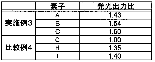
上記実施例1~3とは別の方法を用い、極小凸部を有すサファイア基板を作製した。 <Example 4>
Using a method different from those in Examples 1 to 3, a sapphire substrate having a minimal convex portion was produced.
円筒状マスタースタンパの基材としては、実施例1及び実施例2と同様のものを使用した。実施例1及び実施例2と同様に、レジスト膜を成膜した。 <Production of cylindrical master stamper (mold for resin mold production)>
As the base material of the cylindrical master stamper, the same material as in Example 1 and Example 2 was used. A resist film was formed in the same manner as in Example 1 and Example 2.
得られた円筒状マスタースタンパの表面に対し、実施例1及び実施例2と同様に離型処理を施した。 <Production of resin mold>
A release treatment was performed on the surface of the obtained cylindrical master stamper in the same manner as in Example 1 and Example 2.
1.紫外線を照射の積算光量を1200mJ/cm2にしたこと。
2.ニップロールの押圧力を0.01Mpaにしたこと。 Next, a reel-shaped resin mold was produced using the obtained cylindrical master stamper. The manufacturing conditions of the resin mold were the same as in Example 1 and Example 2 except for the following two items.
1. The accumulated light quantity of irradiation with ultraviolet rays should be 1200 mJ / cm 2 .
2. The pressing force of the nip roll was set to 0.01 MPa.
次に、リール状樹脂モールドG1を鋳型として、反転樹脂モールドを製造した。反転樹脂モールドの製造条件は、紫外線の積算光量を1300mJ/m2にしたこと以外、実施例1及び実施例2と同様にした。以下、得られた複数の凹部より構成される微細パタンを具備する反転樹脂モールドをリール状樹脂モールドG2と称す。 <Production of reverse resin mold>
Next, an inverted resin mold was manufactured using the reel-shaped resin mold G1 as a mold. The manufacturing conditions of the reversal resin mold were the same as those in Example 1 and Example 2 except that the integrated light quantity of ultraviolet rays was 1300 mJ / m 2 . Hereinafter, the obtained reverse resin mold having a fine pattern composed of a plurality of concave portions is referred to as a reel-shaped resin mold G2.
リール状樹脂モールドG2のナノ構造面に対して、下記材料2の希釈液を塗工した。続いて、材料2をナノ構造内部に内包するリール状樹脂モールドのナノ構造面上に、下記材料3の希釈液を塗工し、ナノ加工用フィルムを得た。 <Production of nano-processing film>
The diluted solution of the following
材料3…Bindingpolymer:SR833:SR368:I.184:I.369=77.1g:11.5g:11.5g:1.47g:0.53g
Bindingpolymer…ベンジルメタクリレート80質量%、メタクリル酸20質量%の2元共重合体のメチルエチルケトン溶液(固形分50%、重量平均分子量56000、酸当量430、分散度2.7)
・TTB…チタニウム(IV)テトラブトキシドモノマー(和光純薬工業社製)
・SH710…フェニル変性シリコーン(東レ・ダウコーニング社製)
・3APTMS…3-アクリロキシプロピルトリメトキシシラン(KBM5103(信越シリコーン社製))
・I.184…1-ヒドロキシシクロヘキシルフェニルケトン(BASF社製 Irgacure(登録商標) 184)
・I.369…2-ベンジル-2-ジメチルアミノ-1-(4-モルフォリノフェニル)-ブタノン-1(BASF社製 Irgacure(登録商標) 369)
・SR833…トリシクロデカンジメタノールジアクリレート(SR833(SARTOMER社製))
・SR368…トリス(2-ヒドロキシエチル)イソシアヌレートトリアクリレート(SR833(SARTOMER社製)
Binding polymer: methyl ethyl ketone solution of binary copolymer of 80% by mass of benzyl methacrylate and 20% by mass of methacrylic acid (solid content 50%, weight average molecular weight 56000, acid equivalent 430, dispersity 2.7)
-TTB: Titanium (IV) tetrabutoxide monomer (Wako Pure Chemical Industries, Ltd.)
SH710: Phenyl-modified silicone (Toray Dow Corning)
・ 3APTMS ... 3-acryloxypropyltrimethoxysilane (KBM5103 (manufactured by Shin-Etsu Silicone))
・ I. 184 ... 1-hydroxycyclohexyl phenyl ketone (Irgacure (registered trademark) 184 manufactured by BASF)
・ I. 369... 2-Benzyl-2-dimethylamino-1- (4-morpholinophenyl) -butanone-1 (Irgacure (registered trademark) 369, manufactured by BASF)
SR833: Tricyclodecane dimethanol diacrylate (SR833 (manufactured by SARTOMER))
SR368: Tris (2-hydroxyethyl) isocyanurate triacrylate (SR833 (manufactured by SARTOMER))
作製したナノ加工用フィルムを使用し、光学基板を作製した。光学基板としてはc面サファイア基板を使用した。 <Manufacture of optical substrates>
An optical substrate was produced using the produced nano-processing film. A c-plane sapphire substrate was used as the optical substrate.
実施例4と同様にリール状樹脂モールドG1を製造した。ここで、リール状樹脂モールドG1を得る際のニップの押圧力は0.01Mpaとし、光硬化性樹脂の塗布膜厚(固体分の膜厚)を、3000nmから300nmの範囲内で変更した。ここで、塗布膜厚が1500nm以下の場合は、光硬化性樹脂をプロピレングリコールモノメチルエーテル及びアセトンの混合溶剤にて希釈して、膜厚を調整した。リール状樹脂モールドG1を走査型電子顕微鏡と原子間力顕微鏡により観察し、極小凸部の存在確率を求めた。極小凸部の存在確率は1/3.3~1/50000の範囲で調整できることがわかった。 <Example 5>
A reel-shaped resin mold G1 was manufactured in the same manner as in Example 4. Here, the pressing force of the nip at the time of obtaining the reel-shaped resin mold G1 was set to 0.01 Mpa, and the coating thickness of the photocurable resin (the thickness of the solid portion) was changed within the range of 3000 nm to 300 nm. Here, when the coating film thickness was 1500 nm or less, the photocurable resin was diluted with a mixed solvent of propylene glycol monomethyl ether and acetone to adjust the film thickness. The reel-shaped resin mold G1 was observed with a scanning electron microscope and an atomic force microscope, and the existence probability of the minimum convex portion was obtained. It was found that the existence probability of the minimal convex portion can be adjusted in the range of 1 / 3.3 to 1 / 50,000.
・No.…作製した光学基板に対する管理記号
・Z…極小凸部の存在確率
・Tcv-ave…極小凸部を間においた正常凸部の頂点間の距離の平均値
・IQE…内部量子効率
・LEE比…光取り出し効率比 The meanings of the terms described in Table 4 are as follows.
・ No. ... Control code for the optical substrate produced-Z ... Probability of existence of minimal convex part-Tcv-ave ... Average distance between vertices of normal convex part with minimal convex part in between-IQE ... Internal quantum efficiency-LEE ratio ... Light extraction efficiency ratio

まず、c面片面鏡面サファイア(オフ角:0.2°)の鏡面に対してUV-O3処理を行い、表面を親水化すると共に、パーティクルを除去した。続いて、フォトレジスト用のノボラック樹脂に、ナノ粒子を分散させた。続いて、ナノ粒子の分散したノボラック樹脂をスピンコート法によりサファイア基板上に成膜し、120℃のホットプレート上でプリベークを行った。次にリソグラフィを行い、サファイア基板上に多数の平均間隔が3.2μmの正六方配列にて配列した円錐状のドットを作製した。走査型電子顕微鏡により観察したところ、正常凸部と特異凸部と、が確認された。正常凸部は、走査型電子顕微鏡観察より、平均的に以下のようなドット構造であった。
・ドットの頂点は、曲率半径が0超の丸みを帯びた角部であった。
・ドットの底部の輪郭形状は、略円形であった。
・ドットの側面は2段階の傾斜角度を有していた。この2段階の傾斜角度は、ドットの底部側の方が上部側よりも傾斜角度の小さな傾斜を有していた。
・ドットの底部の径は、1.7μmであった。 <Example 6>
First, the mirror surface of c-plane single-sided mirror sapphire (off angle: 0.2 °) was subjected to UV-O3 treatment to make the surface hydrophilic and remove particles. Subsequently, nanoparticles were dispersed in a novolak resin for photoresist. Subsequently, a novolak resin in which nanoparticles were dispersed was formed on a sapphire substrate by spin coating, and prebaked on a 120 ° C. hot plate. Next, lithography was performed to produce conical dots arranged in a regular hexagonal array with an average interval of 3.2 μm on a sapphire substrate. When observed with a scanning electron microscope, normal convex portions and unique convex portions were confirmed. The normal convex part has the following dot structure on average from observation with a scanning electron microscope.
-The vertex of the dot was a rounded corner with a radius of curvature exceeding zero.
-The outline shape of the bottom of the dot was substantially circular.
-The side surface of the dot had a two-step inclination angle. The two-step inclination angle was such that the bottom side of the dot had a smaller inclination angle than the upper side.
-The diameter of the bottom of the dot was 1.7 μm.
・正常凸部…凹凸構造を構成する複数のドットの中で、特異凸部ではないもの。
・Pave…凹凸構造の平均間隔
・Have…凹凸構造の平均高さ
・φave…凹凸構造のドットの底部の径の平均値
・特異凸部…表面に凸状体又は/及び凹状体を有す凸部
・存在…特異凸部が存在するか否か。〇にて特異凸部が含まれ、×にて含まれないことを意味する。
・被覆率…特異凸部の表面に対する凸状体及び凹状体の平面占有率
・P/R…特異凸部の存在割合
・N…特異凸部の存在割合を求めるのにカウントした凸部の数
・比…特異凸部の存在割合 The meanings of terms in Tables 5 and 6 are as follows.
-Normal convex portion: A plurality of dots constituting the concave-convex structure that are not unique convex portions.
・ Pave: average interval of the concavo-convex structure ・ Have: average height of the concavo-convex structure ・ φave: average value of the diameter of the bottom of the dot of the concavo-convex structure ・ singular convex part: convex having a convex body or / and a concave body on the surface Part / Existence: Whether there is a unique convex part. It means that a singular convex part is included at ◯ and not included at x.
Covering ratio: plane occupancy ratio of convex bodies and concave bodies with respect to the surface of the specific convex parts P / R: existence ratio of the specific convex parts N: number of convex parts counted to determine the existence ratio of the specific convex parts・ Ratio… Existence ratio of unique convex part


表面に凹凸構造面を具備する光学基板を作製し、該基板を使用して半導体発光素子(LED)を作製し、LEDの効率を比較した。 <Example 7 and Example 8>
An optical substrate having a concavo-convex structure surface on the surface was prepared, a semiconductor light emitting device (LED) was manufactured using the substrate, and the efficiency of the LED was compared.
サファイア基板のC面(0001)上に、エッチングマスクとなるSiO2膜を成膜し、フォトリソグラフィ法によりパターニングした。続いて、SiO2から構成されるマスクを利用し、サファイア基板をエッチングすることで凹凸構造Lを作製した。なお、エッチングはウェットエッチングにより行い、エッチング液として、リン酸と硫酸の混酸を用いた。液温は概ね295℃であった。 · Uneven structure C plane of manufacturing sapphire substrate L (0001) on the SiO 2 film serving as an etching mask is formed and patterned by photolithography. Subsequently, the concavo-convex structure L was produced by etching the sapphire substrate using a mask made of SiO 2 . Etching was performed by wet etching, and a mixed acid of phosphoric acid and sulfuric acid was used as an etchant. The liquid temperature was approximately 295 ° C.
・配列…凹凸構造Lの凸部の配列
・PL…凹凸構造Lの平均間隔
・Have…凹凸構造Lの平均高さ
・lcvb…凹凸構造Lの凸部底部幅 The meanings of the terms listed in Table 7 are as follows.
-Arrangement: Arrangement of projections and depressions of concavo-convex structure L-PL ... Average interval of concavo-convex structure L-Have ... Average height of concavo-convex structure L-lcvb ... Bottom width of projections of concavo-convex structure L
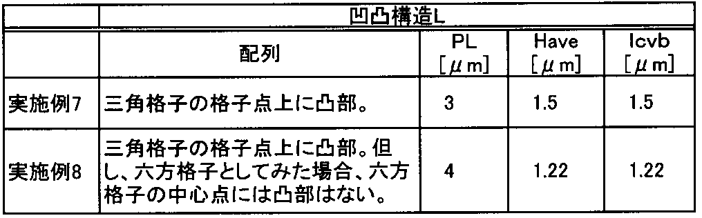
凹凸構造Lの表面上に凹凸構造Sを作製した。 -Production of concavo-convex structure S The concavo-convex structure S was produced on the surface of the concavo-convex structure L.
実施例1と同様の操作を行い、円筒状マスターモールドを得た。 (1) Production of cylindrical master mold The same operation as in Example 1 was performed to obtain a cylindrical master mold.
作製した円筒状マスターモールドを鋳型とし、光ナノインプリント法を適用し、連続的にリール状樹脂モールドG1を作製した。続いて、リール状樹脂モールドG1をテンプレートとして、光ナノインプリント法により、連続的にリール状樹脂モールドG2を得た。 (2) Production of reel-shaped resin mold Using the produced cylindrical master mold as a mold, the optical nanoimprint method was applied to continuously produce a reel-shaped resin mold G1. Subsequently, a reel-shaped resin mold G2 was continuously obtained by an optical nanoimprint method using the reel-shaped resin mold G1 as a template.
リール状樹脂モールドG2をナノ加工用フィルムへと加工した。手順は実施例4と同様とした。但し、材料3を塗工する際に、ナノ構造内部に配置された材料2と塗工された材料3の界面と、材料3の表面と、の距離を1800nmとし、材料3を塗工した後に、95℃の送風乾燥炉内を5分間かけて通過させた。 (3) Production of nano-processing film The reel-shaped resin mold G2 was processed into a nano-processing film. The procedure was the same as in Example 4. However, when the
作製したナノ加工用フィルムを使用し、凹凸構造Lを具備する光学基板の加工を試みた。凹凸構造Lを具備する光学基板としては、表7に記載の基板を使用した。 (4) Nano processing of optical substrate having concavo-convex structure L Using the produced nano-processing film, processing of an optical substrate having concavo-convex structure L was attempted. As the optical substrate having the concavo-convex structure L, the substrates listed in Table 7 were used.
・PS…凹凸構造Sの平均間隔
・Have…凹凸構造Sの平均凸部高さ
・lcvb…凹凸構造Sの凸部底部幅
・PL/PS…凹凸構造Lの平均間隔(PL)と凹凸構造Sの平均間隔(PS)と、の比率
・被覆…凹凸構造Sの凹凸構造Lの凸部及び凹部に対する被覆率 The meanings of the terms described in Table 8 are as follows.
PS: average interval of the concavo-convex structure S. Have: average height of the convex portion of the concavo-convex structure S. lcvb: width of the bottom of the convex portion of the concavo-convex structure S. PL / PS: average interval (PL) of the concavo-convex structure L and the concavo-convex structure S. The ratio of the average interval (PS) to the ratio / covering: the coverage ratio of the concavo-convex structure L of the concavo-convex structure S to the convex and concave portions

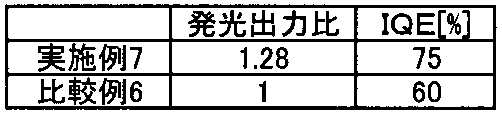

実施例9の凹凸構造(L)を、実施例7と同様に作製、凹凸構造(L)に対して凹凸構造(S)を更に作製した。ここで、凹凸構造(S)の製造方法は実施例7と同様にし、ナノ加工用フィルムのナノ構造を変化させた。ナノ加工用フィルムのナノ構造をパラメータに設定し、実施例7と同様にして光学基板を得、半導体発光素子を作製し、評価した。なお、凹凸構造(S)は、凹凸構造(L)の凸部頂部、凸部側面そして凹部底部に作製されていた。 <Example 9>
The concavo-convex structure (L) of Example 9 was produced in the same manner as in Example 7, and a concavo-convex structure (S) was further produced with respect to the concavo-convex structure (L). Here, the manufacturing method of the concavo-convex structure (S) was the same as in Example 7, and the nanostructure of the film for nanoprocessing was changed. The nanostructure of the film for nanofabrication was set as a parameter, an optical substrate was obtained in the same manner as in Example 7, and a semiconductor light emitting device was produced and evaluated. In addition, the concavo-convex structure (S) was produced on the convex top part, convex part side surface, and concave part bottom part of the concavo-convex structure (L).
・PS…凹凸構造Sの平均間隔
・Have…凹凸構造Sの平均凸部高さ
・lcvb…凹凸構造Sの凸部底部幅
・PL/PS…凹凸構造Lの平均間隔(PL)と凹凸構造Sの平均間隔(PS)と、の比率
・被覆…凹凸構造Sの凹凸構造Lの凸部及び凹部に対する被覆率 The meanings of the terms described in Table 11 are as follows.
PS: average interval of the concavo-convex structure S. Have: average height of the convex portion of the concavo-convex structure S. lcvb: width of the bottom of the convex portion of the concavo-convex structure S. PL / PS: average interval (PL) of the concavo-convex structure L and the concavo-convex structure S. The ratio of the average interval (PS) to the ratio / covering: the coverage ratio of the concavo-convex structure L of the concavo-convex structure S to the convex and concave portions

凹凸構造(L)の凸部頂部上面にのみ凹凸構造(S)を具備した光学基板を作製した。 <Example 10>
An optical substrate having a concavo-convex structure (S) only on the top surface of the convex top of the concavo-convex structure (L) was produced.
リール状樹脂モールドG2をナノ加工用フィルムへと加工した。手順は実施例4と同様とした。但し、材料3を塗工する際に、ナノ構造内部に配置された材料2と塗工された材料3の界面と、材料3の表面と、の距離を350nmとし、材料3を塗工した後に、95℃の送風乾燥炉内を5分間かけて通過させた。 (3) Production of nano-processing film The reel-shaped resin mold G2 was processed into a nano-processing film. The procedure was the same as in Example 4. However, when the
作製したナノ加工用フィルムを使用し、光学基板を加工し、凹凸構造(S)を作製した。 (4) Nano-processing of optical substrate Using the prepared film for nano-processing, the optical substrate was processed to prepare a concavo-convex structure (S).
・平均間隔Paveが3.2μmであり、正六方配列している。
・ドットの底部径は、2.4μmであり、底部形状は略円形。
・ドット間の凹部底部は平坦であった。
・ドット頂部に平坦面のある円錐台形状。ドット頂部の平坦面は略円形であり、その直径は1.6μmであった。
・ドット頂部は略円形のテーブルトップであり、ドット頂部上にのみ凹凸構造(S)が配置されていた。 The obtained optical substrate was observed with a scanning electron microscope. The dot-shaped uneven structure (L) was the following dot-shaped body.
The average interval Pave is 3.2 μm, and regular hexagons are arranged.
-The bottom diameter of the dot is 2.4 μm, and the bottom shape is substantially circular.
-The bottom of the recess between the dots was flat.
-A truncated cone shape with a flat surface at the top of the dot. The flat surface at the top of the dot was substantially circular, and its diameter was 1.6 μm.
The dot top was a substantially circular table top, and the concavo-convex structure (S) was arranged only on the dot top.
・平均間隔Paveが3.2μmであり、正六方配列している。
・ホールの開口部径は、1.5μmであり、開口形状は略円形。
・ホールの深さは、1.4μm。
・ホール間の凸部頂部は平坦であり、この平坦面上にのみ凹凸構造(S)が配置されていた。
・ホールの形状は底面が略円形の円錐であり、円錐の頂部は曲率半径が0超の角部であった。 On the other hand, the hole-shaped uneven structure (L) was the following hole-shaped body.
The average interval Pave is 3.2 μm, and regular hexagons are arranged.
-The opening diameter of the hole is 1.5 μm, and the opening shape is substantially circular.
・ The depth of the hole is 1.4μm.
-The convex part top part between holes was flat, and the uneven structure (S) was arrange | positioned only on this flat surface.
The shape of the hole was a cone having a substantially circular bottom surface, and the top of the cone was a corner with a radius of curvature exceeding zero.
・PS…凹凸構造Sの平均間隔
・Have…凹凸構造Sの平均凸部高さ
・lcvb…凹凸構造Sの凸部底部幅
・PL/PS…凹凸構造Lの平均間隔(PL)と凹凸構造Sの平均間隔(PS)と、の比率
・被覆1…凹凸構造Sの凹凸構造Lの凸部及び凹部に対する被覆率
・被覆2…凹凸構造Lの凸部頂部上面に対する凹凸構造Sの被覆率T The meanings of the terms described in Table 12 are as follows.
PS: average interval of the concavo-convex structure S. Have: average height of the convex portion of the concavo-convex structure S. lcvb: width of the bottom of the convex portion of the concavo-convex structure S. PL / PS: average interval (PL) of the concavo-convex structure L and the concavo-convex structure S. The ratio between the average interval (PS) of the projections and depressions of the concavo-convex structure S and the coverage of the concavo-convex structure L of the concavo-convex structure S.

・PS…凹凸構造Sの平均間隔
・Have…凹凸構造Sの平均凸部高さ
・lcvb…凹凸構造Sの凸部底部幅
・PL/PS…凹凸構造Lの平均間隔(PL)と凹凸構造Sの平均間隔(PS)と、の比率
・被覆1…凹凸構造Sの凹凸構造Lの凸部及び凹部に対する被覆率
・被覆2…凹凸構造Lの凸部頂部上面に対する凹凸構造Sの被覆率T The meanings of the terms described in Table 13 are as follows.
PS: average interval of the concavo-convex structure S. Have: average height of the convex portion of the concavo-convex structure S. lcvb: width of the bottom of the convex portion of the concavo-convex structure S. PL / PS: average interval (PL) of the concavo-convex structure L and the concavo-convex structure S. The ratio between the average interval (PS) of the projections and depressions of the concavo-convex structure S and the coverage of the concavo-convex structure L of the concavo-convex structure S.

積層体マスクを構成する材料として、第1のマスク層に酸化クロム、第2のマスク層に酸化シリコンを選択した。なお、後述の、第1のマスク層(酸化クロム層)及びサファイア基板のウェットエッチングに用いるエッチング液に対する酸化クロムとサファイア基板とのエッチング選択比は3であり、酸化シリコンとサファイア基板とのエッチング選択比は20以上である。 <Example 11>
As materials constituting the laminate mask, chromium oxide was selected for the first mask layer and silicon oxide was selected for the second mask layer. In addition, the etching selectivity of the chromium oxide and the sapphire substrate with respect to an etching solution used for wet etching of the first mask layer (chromium oxide layer) and the sapphire substrate, which will be described later, is 3, and the etching selection between the silicon oxide and the sapphire substrate is performed. The ratio is 20 or more.
マスクを構成する材料として、第1のマスク層に酸化シリコンと酸化タングステンから成る混合物、第2のマスク層に酸化シリコンを選択した。該マスクの組成比はシリコンとタングステンとの比率が、9mol%:1mol%に設定した。なお、後述の、第1のマスク層(酸化シリコン)及びサファイア基板のウェットエッチングに用いるエッチング液に対する、酸化シリコンと酸化タングステンから成る混合物とサファイア基板とのエッチング選択比は3であり、酸化シリコンとサファイア基板とのエッチング選択比は20以上である。 <Example 12>
As materials constituting the mask, a mixture of silicon oxide and tungsten oxide was selected for the first mask layer, and silicon oxide was selected for the second mask layer. The composition ratio of the mask was set such that the ratio of silicon to tungsten was 9 mol%: 1 mol%. Note that the etching selectivity of a mixture of silicon oxide and tungsten oxide and a sapphire substrate with respect to an etching solution used for wet etching of a first mask layer (silicon oxide) and a sapphire substrate, which will be described later, is 3, and The etching selectivity with the sapphire substrate is 20 or more.
・DACHP…OPTOOL DAC HP(ダイキン工業社製)
・M350…トリメチロールプロパン(EO変性)トリアクリレート(東亞合成社製 M350)
・I.184…Irgacure 184(BASFジャパン(株)製)
・I.369…Irgacure 369(BASFジャパン(株)製)
・TTB…チタンテトラブトキシド
・3APTMS…KBM5103(信越シリコーン社製)
・SH710…フェニル変性シリコーン(東レ・ダウコーニング社製)
・SR833…トリシクロデカンジメタノールジアクリレート(SR833(SARTOMER社製))
・SR368…トリス(2-ヒドロキシエチル)イソシアヌレートトリアクリレート(SR368(SARTOMER社製) In this example, the following materials were used.
・ DACHP: OPTOOL DAC HP (manufactured by Daikin Industries)
M350: trimethylolpropane (EO-modified) triacrylate (M350, manufactured by Toagosei Co., Ltd.)
・ I. 184 ... Irgacure 184 (manufactured by BASF Japan)
・ I. 369 ... Irgacure 369 (manufactured by BASF Japan Ltd.)
・ TTB: Titanium tetrabutoxide ・ 3APTMS: KBM5103 (manufactured by Shin-Etsu Silicone)
SH710: Phenyl-modified silicone (Toray Dow Corning)
SR833: Tricyclodecane dimethanol diacrylate (SR833 (manufactured by SARTOMER))
SR368: Tris (2-hydroxyethyl) isocyanurate triacrylate (SR368 (manufactured by SARTOMER)
半導体レーザを用いた直接描画リソグラフィ法により、円筒状石英ガラスの表面に、凹凸構造を形成した。まず、円筒状石英ガラス表面上に、スパッタリング法によりレジスト層を成膜した。スパッタリング法は、ターゲット(レジスト層)として、φ3インチのCuO(8atm%Si含有)を用いて、RF100Wの電力で実施し、20nmのレジスト層を成膜した。続いて、円筒状石英ガラスを回転させながら、波長405nmn半導体レーザを用い露光を行った。次に、露光後のレジスト層を現像した。レジスト層の現像は、0.03wt%のグリシン水溶液を用いて、240sec処理とした。次に、現像したレジスト層をマスクとし、ドライエッチングによるエッチング層(石英ガラス)のエッチングを行った。ドライエッチングは、エッチングガスとしてSF6を用い、処理ガス圧1Pa、処理電力300W、処理時間5分の条件で実施した。最後に、表面に凹凸構造が付与された円筒状石英ガラスから、レジスト層残渣のみを、pH1の硫酸を用い剥離した。剥離時間は6分間とした。 (1) Production of cylindrical master mold An uneven structure was formed on the surface of cylindrical quartz glass by a direct drawing lithography method using a semiconductor laser. First, a resist layer was formed on the cylindrical quartz glass surface by sputtering. The sputtering method was carried out using φ3 inch CuO (containing 8 atm% Si) as a target (resist layer) with a power of RF 100 W to form a 20 nm resist layer. Subsequently, exposure was performed using a semiconductor laser having a wavelength of 405 nm while rotating the cylindrical quartz glass. Next, the resist layer after exposure was developed. The development of the resist layer was performed for 240 seconds using a 0.03 wt% glycine aqueous solution. Next, using the developed resist layer as a mask, the etching layer (quartz glass) was etched by dry etching. Dry etching was performed using SF6 as an etching gas under the conditions of a processing gas pressure of 1 Pa, a processing power of 300 W, and a processing time of 5 minutes. Finally, only the resist layer residue was peeled off from the cylindrical quartz glass having a concavo-convex structure on the surface using sulfuric acid having a pH of 1. The peeling time was 6 minutes.
作製した円筒状マスターモールドを鋳型とし、光ナノインプリント法を適用し、連続的にリール状の樹脂モールドG1を作製した。続いて、リール状の樹脂モールドG1をテンプレートとして、光ナノインプリント法により、連続的にリール状の樹脂モールドG2を得た。樹脂モールドG2を得ることで、円筒状マスターモールドと同一のパターン形状を得た。以下に樹脂モールドG1、G2の作製方法を詳説する。 (2) Production of reel-shaped resin mold Using the produced cylindrical master mold as a mold, the optical nanoimprint method was applied to continuously produce a reel-shaped resin mold G1. Subsequently, a reel-shaped resin mold G2 was continuously obtained by an optical nanoimprint method using the reel-shaped resin mold G1 as a template. By obtaining the resin mold G2, the same pattern shape as the cylindrical master mold was obtained. Hereinafter, a method for producing the resin molds G1 and G2 will be described in detail.
材料A… DACHP:M350:I.184:I.369=17.5g:100g:5.5g:2.0g The following material A was applied to an easily adhesive surface of PET film A-3100 (Toyobo Co., Ltd .:
Material A ... DACHP: M350: I. 184: I.D. 369 = 17.5 g: 100 g: 5.5 g: 2.0 g
リール状の樹脂モールドG2の凹凸構造面に対して、下記材料Bの希釈液を塗工した。続いて、材料Bを凹凸構造内部に内包するリール状の樹脂モールドG2の凹凸構造面上に、下記材料Cの希釈液を塗工し、ナノ加工用フィルムを得た。
材料B…TTB:3APTMS:SH710:I.184:I.369=65.2g:34.8g:5.0g:1.9g:0.7g
材料C…Bindingpolymer:SR833:SR368:I.184:I.369=77.1g:11.5g:11.5g:1.47g:0.53g
Bindingpolymer…ベンジルメタクリレート80質量%、メタクリル酸20質量%の2元共重合体のメチルエチルケトン溶液(固形分50%、重量平均分子量56000、酸当量330、分散度2.7) (3) Production of Nano-Processing Film A diluent for the following material B was applied to the concavo-convex structure surface of the reel-shaped resin mold G2. Subsequently, a dilution liquid of the following material C was applied on the concavo-convex structure surface of the reel-shaped resin mold G2 including the material B inside the concavo-convex structure to obtain a nano-processing film.
Material B ... TTB: 3APTMS: SH710: I. 184: I.D. 369 = 65.2 g: 34.8 g: 5.0 g: 1.9 g: 0.7 g
Material C: Binding polymer: SR833: SR368: I.I. 184: I.D. 369 = 77.1 g: 11.5 g: 11.5 g: 1.47 g: 0.53 g
Binding polymer: Methyl ethyl ketone solution of a binary copolymer of 80% by mass of benzyl methacrylate and 20% by mass of methacrylic acid (solid content 50%, weight average molecular weight 56000, acid equivalent 330, dispersity 2.7)
マスクを構成する材料として、サファイア基板のウェットエッチングに用いるエッチング液に対して耐性がある材料の酸化シリコンを選択した。なお、後述のサファイア基板のウェットエッチング液に対する酸化シリコンとサファイア基板とのエッチング選択比は20以上である。 <Example 13>
As a material constituting the mask, silicon oxide was selected as a material resistant to an etching solution used for wet etching of the sapphire substrate. Note that the etching selectivity of the silicon oxide and the sapphire substrate with respect to the wet etching solution of the sapphire substrate described later is 20 or more.
マスクを構成する材料として、サファイア基板のウェットエッチングに用いるエッチング液に対して耐性がない材料の酸化クロムを選択した。なお、後述のサファイア基板のウェットエッチング液に対する酸化クロムとサファイア基板とのエッチング選択比は3である。 <Example 14>
As a material constituting the mask, chromium oxide was selected as a material having no resistance to an etching solution used for wet etching of the sapphire substrate. In addition, the etching selectivity of the chromium oxide and the sapphire substrate with respect to the wet etching liquid of the sapphire substrate described later is 3.
マスクを構成する材料として、サファイア基板のウェットエッチングに用いるエッチング液に対して耐性がない材料の酸化シリコンと酸化タングステンから成る混合物を選択した。該マスクの組成比は、シリコンとタングステンとの比率が、9mol%:1mol%になるように設定した。なお、後述のサファイア基板のウェットエッチング液に対する酸化シリコンと酸化タングステンの混合物とサファイア基板とのエッチング選択比は3である。 <Example 15>
As a material constituting the mask, a mixture of silicon oxide and tungsten oxide, which is a material that is not resistant to an etchant used for wet etching of the sapphire substrate, was selected. The composition ratio of the mask was set so that the ratio of silicon to tungsten was 9 mol%: 1 mol%. Note that the etching selection ratio of the mixture of silicon oxide and tungsten oxide and the sapphire substrate with respect to the wet etching solution of the sapphire substrate described later is 3.
マスクを構成する材料として、実施例3と同様のサファイア基板のウェットエッチングに用いるエッチング液に対して耐性がない材料の酸化シリコンと酸化タングステンから成る混合物を選択した。該マスクの組成比は、シリコンとタングステンとの比率が、9mol%:1mol%になるように設定した。なお、後述のサファイア基板のウェットエッチング液に対する酸化シリコンと酸化タングステンの混合物とサファイア基板とのエッチング選択比は3である。 <Example 16>
As a material constituting the mask, a mixture composed of silicon oxide and tungsten oxide, which is a material that is not resistant to the etching solution used for wet etching of the sapphire substrate similar to that in Example 3, was selected. The composition ratio of the mask was set so that the ratio of silicon to tungsten was 9 mol%: 1 mol%. Note that the etching selection ratio of the mixture of silicon oxide and tungsten oxide and the sapphire substrate with respect to the wet etching solution of the sapphire substrate described later is 3.
・DACHP…OPTOOL DAC HP(ダイキン工業社製)
・M350…トリメチロールプロパン(EO変性)トリアクリレート(東亞合成社製 M350)
・I.184…Irgacure 184(BASFジャパン(株)製)
・I.369…Irgacure 369(BASFジャパン(株)製)
・TTB…チタンテトラブトキシド
・3APTMS…KBM5103(信越シリコーン社製)
・SH710…フェニル変性シリコーン(東レ・ダウコーニング社製)
・SR833…トリシクロデカンジメタノールジアクリレート(SR833(SARTOMER社製))
・SR368…トリス(2-ヒドロキシエチル)イソシアヌレートトリアクリレート(SR368(SARTOMER社製) In this example, the following materials were used.
・ DACHP: OPTOOL DAC HP (manufactured by Daikin Industries)
M350: trimethylolpropane (EO-modified) triacrylate (M350, manufactured by Toagosei Co., Ltd.)
・ I. 184 ... Irgacure 184 (manufactured by BASF Japan)
・ I. 369 ... Irgacure 369 (manufactured by BASF Japan Ltd.)
・ TTB: Titanium tetrabutoxide ・ 3APTMS: KBM5103 (manufactured by Shin-Etsu Silicone)
SH710: Phenyl-modified silicone (Toray Dow Corning)
SR833: Tricyclodecane dimethanol diacrylate (SR833 (manufactured by SARTOMER))
SR368: Tris (2-hydroxyethyl) isocyanurate triacrylate (SR368 (manufactured by SARTOMER)
半導体レーザを用いた直接描画リソグラフィ法により、円筒状石英ガラスの表面に、凹凸構造を形成した。まず、円筒状石英ガラス表面上に、スパッタリング法によりレジスト層を成膜した。スパッタリング法は、ターゲット(レジスト層)として、φ3インチのCuO(8atm%Si含有)を用いて、RF100Wの電力で実施し、20nmのレジスト層を成膜した。続いて、円筒状石英ガラスを回転させながら、波長405nmn半導体レーザを用い露光を行った。次に、露光後のレジスト層を現像した。レジスト層の現像は、0.03wt%のグリシン水溶液を用いて、240sec処理とした。次に、現像したレジスト層をマスクとし、ドライエッチングによるエッチング層(石英ガラス)のエッチングを行った。ドライエッチングは、エッチングガスとしてSF6を用い、処理ガス圧1Pa、処理電力300W、処理時間5分の条件で実施した。最後に、表面に凹凸構造が付与された円筒状石英ガラスから、レジスト層残渣のみを、pH1の硫酸を用い剥離した。剥離時間は6分間とした。 (1) Production of cylindrical master mold An uneven structure was formed on the surface of cylindrical quartz glass by a direct drawing lithography method using a semiconductor laser. First, a resist layer was formed on the cylindrical quartz glass surface by sputtering. The sputtering method was carried out using φ3 inch CuO (containing 8 atm% Si) as a target (resist layer) with a power of RF 100 W to form a 20 nm resist layer. Subsequently, exposure was performed using a semiconductor laser having a wavelength of 405 nm while rotating the cylindrical quartz glass. Next, the resist layer after exposure was developed. The development of the resist layer was performed for 240 seconds using a 0.03 wt% glycine aqueous solution. Next, using the developed resist layer as a mask, the etching layer (quartz glass) was etched by dry etching. Dry etching was performed using SF6 as an etching gas under the conditions of a processing gas pressure of 1 Pa, a processing power of 300 W, and a processing time of 5 minutes. Finally, only the resist layer residue was peeled off from the cylindrical quartz glass having a concavo-convex structure on the surface using sulfuric acid having a pH of 1. The peeling time was 6 minutes.
作製した円筒状マスターモールドを鋳型とし、光ナノインプリント法を適用し、連続的にリール状の樹脂モールドG1を作製した。続いて、リール状の樹脂モールドG1をテンプレートとして、光ナノインプリント法により、連続的にリール状の樹脂モールドG2を得た。樹脂モールドG2を得ることで、円筒状マスターモールドと同一のパターン形状を得た。以下に樹脂モールドG1、G2の作製方法を詳説する。 (2) Production of reel-shaped resin mold Using the produced cylindrical master mold as a mold, the optical nanoimprint method was applied to continuously produce a reel-shaped resin mold G1. Subsequently, a reel-shaped resin mold G2 was continuously obtained by an optical nanoimprint method using the reel-shaped resin mold G1 as a template. By obtaining the resin mold G2, the same pattern shape as the cylindrical master mold was obtained. Hereinafter, a method for producing the resin molds G1 and G2 will be described in detail.
材料A… DACHP:M350:I.184:I.369=17.5g:100g:5.5g:2.0g The following material A was applied to an easily adhesive surface of PET film A-4100 (manufactured by Toyobo Co., Ltd .:
Material A ... DACHP: M350: I. 184: I.D. 369 = 17.5 g: 100 g: 5.5 g: 2.0 g
リール状の樹脂モールドG2の凹凸構造面に対して、下記材料Bの希釈液を塗工した。続いて、材料Bを凹凸構造内部に内包するリール状の樹脂モールドG2の凹凸構造面上に、下記材料Cの希釈液を塗工し、ナノ加工用フィルムを得た。
材料B…TTB:3APTMS:SH710:I.184:I.369=65.2g:34.8g:5.0g:1.9g:0.7g
材料C…Bindingpolymer:SR833:SR368:I.184:I.369=77.1g:11.5g:11.5g:1.47g:0.53g
Bindingpolymer…ベンジルメタクリレート80質量%、メタクリル酸20質量%の2元共重合体のメチルエチルケトン溶液(固形分50%、重量平均分子量56000、酸当量430、分散度2.7) (3) Production of Nano-Processing Film A diluent for the following material B was applied to the concavo-convex structure surface of the reel-shaped resin mold G2. Subsequently, a dilution liquid of the following material C was applied on the concavo-convex structure surface of the reel-shaped resin mold G2 including the material B inside the concavo-convex structure to obtain a nano-processing film.
Material B ... TTB: 3APTMS: SH710: I. 184: I.D. 369 = 65.2 g: 34.8 g: 5.0 g: 1.9 g: 0.7 g
Material C: Binding polymer: SR833: SR368: I.I. 184: I.D. 369 = 77.1 g: 11.5 g: 11.5 g: 1.47 g: 0.53 g
Binding polymer: methyl ethyl ketone solution of binary copolymer of 80% by mass of benzyl methacrylate and 20% by mass of methacrylic acid (solid content 50%, weight average molecular weight 56000, acid equivalent 430, dispersity 2.7)
This application is based on Japanese Patent Application Japanese Patent Application No. 2012-084208 filed on April 2, 2012, Japanese Patent Application Japanese Patent Application No. 2012-1034889 filed on April 27, 2012, and Japanese Patent Application Special Application filed on April 27, 2012. Japanese Patent Application No. 2012-103490, Japanese Patent Application Japanese Patent Application No. 2012-227295 filed on October 12, 2012, Japanese Patent Application Japanese Patent Application No. 2012-267377 filed on December 6, 2012, Japanese Patent Application filed on December 6, 2012 Based on Japanese Patent Application No. 2012-267488 and Japanese Patent Application No. 2012-280241 filed on Dec. 21, 2012. All these contents are included here.
Claims (28)
- 基板と、前記基板の表面の一部又は全面に形成された凹凸構造と、を具備する光学基板であって、
前記凹凸構造のうち少なくとも一部の領域は、互いに離間して配置された複数の凸部を有すると共に、前記複数の凸部は、第1の高さを有する複数の第1の凸部と、前記第1の高さよりも低い第2の高さを有する複数の第2の凸部とを含み、
隣接する前記第1の凸部間の平均間隔Paveが、下記式(1)を満たし、且つ、
式(1)
50nm≦Pave≦1500nm
前記第2の凸部は、前記凹凸構造の平均凸部高さHaveに対して下記式(2)の関係を満たす凸部高さhnを有すると共に、前記凹凸構造において下記式(3)を満たす確率Zで存在することを特徴とする光学基板。
式(2)
0.6Have≧hn≧0
式(3)
1/10000≦Z≦1/5 An optical substrate comprising a substrate and a concavo-convex structure formed on a part or the entire surface of the substrate,
At least a part of the concavo-convex structure has a plurality of protrusions arranged apart from each other, and the plurality of protrusions includes a plurality of first protrusions having a first height, A plurality of second protrusions having a second height lower than the first height;
The average interval Pave between the adjacent first convex portions satisfies the following formula (1), and
Formula (1)
50 nm ≦ Pave ≦ 1500 nm
The second convex portion has a convex portion height hn that satisfies the relationship of the following formula (2) with respect to the average convex portion height Have of the concave-convex structure, and satisfies the following formula (3) in the concave-convex structure. An optical substrate characterized by existing with probability Z.
Formula (2)
0.6 Have ≧ hn ≧ 0
Formula (3)
1/10000 ≦ Z ≦ 1/5 - 前記領域が、前記複数の凸部のみで構成されると共に、前記確率Zが1/1000以上1/10以下を満たすことを特徴とする請求項1記載の光学基板。 2. The optical substrate according to claim 1, wherein the region includes only the plurality of convex portions and the probability Z satisfies 1/1000 or more and 1/10 or less.
- 前記第2の凸部を間において隣接する第1の凸部間の平均距離Tcv-aveと、前記隣接する第1の凸部の平均間隔Paveとが、下記式(4)の関係を満たすことを特徴とする請求項1又は請求項2記載の光学基板。
式(4)
1.0Pave<Tcv-ave≦11Pave The average distance Tcv-ave between the first convex portions adjacent to each other between the second convex portions and the average interval Pave between the adjacent first convex portions satisfy the relationship of the following formula (4). The optical substrate according to claim 1, wherein:
Formula (4)
1.0 Pave <Tcv-ave ≦ 11 Pave - 基板と、前記基板の一主面上の表面の一部又は全面に形成された凹凸構造と、を具備する光学基板であって、
前記凹凸構造のうち少なくとも一部の領域は、互いに離間して配置された複数の凹部を有すると共に、前記複数の凹部は、第1の深さを有する複数の第1の凹部と、前記第1の深さよりも浅い第2の深さを有する複数の第2の凹部とを含み、
隣接する前記第1の凹部間の平均間隔Paveが、下記式(5)を満たし、且つ、
式(5)
50nm≦Pave≦1500nm
前記第2の凹部は、前記凹凸構造の平均凹部深さDaveに対して下記式(6)の関係を満たす凹部深さdnを有すると共に、前記凹凸構造において下記式(7)を満たす確率Zで存在することを特徴とする光学基板。
式(6)
0.6Dave≧dn≧0
式(7)
1/10000≦Z≦1/5 An optical substrate comprising a substrate and a concavo-convex structure formed on a part or the entire surface of one main surface of the substrate,
At least a part of the concavo-convex structure has a plurality of recesses that are spaced apart from each other, and the plurality of recesses include a plurality of first recesses having a first depth, and the first A plurality of second recesses having a second depth shallower than the depth of
The average interval Pave between the adjacent first recesses satisfies the following formula (5), and
Formula (5)
50 nm ≦ Pave ≦ 1500 nm
The second recess has a recess depth dn that satisfies the relationship of the following expression (6) with respect to the average recess depth Dave of the uneven structure, and a probability Z that satisfies the following expression (7) in the uneven structure: An optical substrate characterized in that it exists.
Formula (6)
0.6 Dave ≧ dn ≧ 0
Formula (7)
1/10000 ≦ Z ≦ 1/5 - 前記領域は、前記複数の凹部のみで構成されると共に、前記確率Zが1/1000以上1/10以下を満たすことを特徴とする請求項4記載の光学基板。 5. The optical substrate according to claim 4, wherein the region includes only the plurality of concave portions and the probability Z satisfies 1/1000 or more and 1/10 or less.
- 前記第2の凹部を間において隣接する第1の凹部間の平均距離Tcc-aveと、前記隣接する第1の凹部の平均間隔Paveとが、下記式(8)の関係を満たすことを特徴とする請求項4又は請求項5記載の光学基板。
式(8)
1.0Pave<Tcc-ave≦11Pave The average distance Tcc-ave between the first recesses adjacent to each other between the second recesses and the average interval Pave between the adjacent first recesses satisfy the relationship of the following formula (8): The optical substrate according to claim 4 or 5.
Formula (8)
1.0 Pave <Tcc-ave ≦ 11 Pave - 基板と、前記基板の表面の一部又は全面に形成された凹凸構造と、を具備する光学基板であって、
前記凹凸構造のうち少なくとも一部分は、互いに離間して配置された複数の凸部を有すると共に、
前記複数の凸部のうち少なくとも1つの凸部は、表面に少なくとも1以上の凸状体又は凹状体を具備する特異凸部であり、且つ、
前記凹凸構造の平均間隔Paveは、1.5μm以上10μm以下であることを特徴とする光学基板。 An optical substrate comprising a substrate and a concavo-convex structure formed on a part or the entire surface of the substrate,
At least a portion of the concavo-convex structure has a plurality of convex portions arranged apart from each other,
At least one convex portion among the plurality of convex portions is a unique convex portion having at least one convex body or concave body on the surface, and
The optical substrate, wherein an average interval Pave of the uneven structure is 1.5 μm or more and 10 μm or less. - 前記特異凸部は、前記凸状体又は前記凹状体の前記凸部の表面に対する被覆率が0%超100%未満であることを特徴とする請求項7記載の光学基板。 8. The optical substrate according to claim 7, wherein the specific convex portion has a coverage ratio of the convex body or the concave body to the surface of the convex portion of more than 0% and less than 100%.
- 基板本体と、前記基板本体の表面の一部又は全面に形成された凹凸構造と、を具備する光学基板であって、
前記凹凸構造は、前記基板本体の主面上に設けられ、第1の平均間隔(PL)を有する複数の凸部及び凹部で構成された第1の凹凸構造(L)と、
前記第1の凹凸構造(L)を構成する前記凸部及び前記凹部の少なくとも一方の表面上に設けられ、第2の平均間隔(PS)を有する複数の凸部及び凹部で構成された第2の凹凸構造(S)と、を含み、
前記第1の平均間隔(PL)と前記第2の平均間隔(PS)と、の比率(PL/PS)は、1超2000以下であることを特徴とする光学基板。 An optical substrate comprising a substrate body, and a concavo-convex structure formed on a part or the entire surface of the substrate body,
The concavo-convex structure is provided on the main surface of the substrate body, and includes a first concavo-convex structure (L) composed of a plurality of convex portions and concave portions having a first average interval (PL),
The 2nd comprised by the some convex part and recessed part which are provided on the surface of at least one of the said convex part and the said recessed part which comprise the said 1st uneven structure (L), and have 2nd average space | interval (PS). An uneven structure (S) of
The optical substrate, wherein a ratio (PL / PS) of the first average interval (PL) and the second average interval (PS) is more than 1 and 2000 or less. - 前記第1の凹凸構造(L)は、互いに離間した複数の凸部から構成されると共に、少なくとも前記第1の凹凸構造(L)の凹部の底部に前記第2の凹凸構造(S)を構成する凸部又は凹部が設けられていることを特徴とする請求項9記載の光学基板。 The first concavo-convex structure (L) includes a plurality of convex portions spaced apart from each other, and the second concavo-convex structure (S) is configured at least at the bottom of the concave portion of the first concavo-convex structure (L). The optical substrate according to claim 9, wherein a convex portion or a concave portion is provided.
- 前記第1の凹凸構造(L)は、互いに離間した複数の凹部から構成されると共に、少なくとも前記第1の凹凸構造(L)の凸部の頂部に前記第2の凹凸構造(S)を構成する凸部又は凹部が設けられることを特徴とする請求項9記載の光学基板。 The first concavo-convex structure (L) includes a plurality of concave portions spaced apart from each other, and the second concavo-convex structure (S) is formed at least on the top of the convex portion of the first concavo-convex structure (L). The optical substrate according to claim 9, wherein a convex portion or a concave portion is provided.
- 前記第2の凹凸構造(S)の、前記第1の凹凸構造(L)に対する被覆率が0%超100%未満であることを特徴とする請求項9から請求項11のいずれかに記載の光学基板。 The coverage of the second concavo-convex structure (S) with respect to the first concavo-convex structure (L) is more than 0% and less than 100%, according to any one of claims 9 to 11. Optical substrate.
- 基板本体と、前記基板本体の表面の一部又は全面に形成された凹凸構造と、を具備する光学基板であって、
前記凹凸構造は、
前記基板本体の主面上に設けられ、第1の平均間隔(PS)を有する複数の凸部及び凹部で構成された第1の凹凸構造(S)と、
前記第1の凹凸構造(S)の表面上に前記第1の凹凸構造(S)が一部露出するように互いに離間して設けられ、第2の平均間隔(PL)を有する複数の凸部で構成された第2の凹凸構造(L)と、を含み、
前記第1の平均間隔(PS)と前記第2の平均間隔(PL)と、の比率(PL/PS)は、1超2000以下であることを特徴とする光学基板。 An optical substrate comprising a substrate body, and a concavo-convex structure formed on a part or the entire surface of the substrate body,
The uneven structure is
A first concavo-convex structure (S) that is provided on the main surface of the substrate body and includes a plurality of convex portions and concave portions having a first average interval (PS);
A plurality of convex portions provided on the surface of the first concavo-convex structure (S) so as to be partially exposed so as to partially expose the first concavo-convex structure (S) and having a second average interval (PL) A second concavo-convex structure (L) composed of
The optical substrate, wherein a ratio (PL / PS) between the first average interval (PS) and the second average interval (PL) is more than 1 and 2000 or less. - 前記凹凸構造(S)を構成する凸部の径は、底部から頂点へ向かって小さくなることを特徴とする請求項9から請求項13のいずれかに記載の光学基板。 The optical substrate according to any one of claims 9 to 13, wherein a diameter of the convex portion constituting the concave-convex structure (S) decreases from the bottom toward the apex.
- 前記第2の凹凸構造(S)のうち少なくとも一部の領域は、互いに離間して配置された複数の凸部を有すると共に、前記複数の凸部は、第1の高さを有する複数の第1の凸部と、前記第1の高さよりも低い第2の高さを有する複数の第2の凸部とを含み、
隣接する前記第1の凸部間の平均間隔Paveが、下記式(1)を満たし、且つ、
式(1)
50nm≦Pave≦1500nm
前記第2の凸部は、前記凹凸構造の平均凸部高さHaveに対して下記式(2)の関係を満たす凸部高さhnを有すると共に、前記凹凸構造において下記式(3)を満たす確率Zで存在することを特徴とする請求項9から請求項14のいずれかに記載の光学基板。
式(2)
0.6Have≧hn≧0
式(3)
1/10000≦Z≦1/5 At least a part of the second concavo-convex structure (S) has a plurality of protrusions arranged apart from each other, and the plurality of protrusions have a plurality of first heights having a first height. One convex portion and a plurality of second convex portions having a second height lower than the first height,
The average interval Pave between the adjacent first convex portions satisfies the following formula (1), and
Formula (1)
50 nm ≦ Pave ≦ 1500 nm
The second convex portion has a convex portion height hn that satisfies the relationship of the following formula (2) with respect to the average convex portion height Have of the concave-convex structure, and satisfies the following formula (3) in the concave-convex structure. The optical substrate according to any one of claims 9 to 14, wherein the optical substrate exists with a probability Z.
Formula (2)
0.6 Have ≧ hn ≧ 0
Formula (3)
1/10000 ≦ Z ≦ 1/5 - 前記領域が、前記複数の凸部のみで構成されることを特徴とする請求項15記載の光学基板。 The optical substrate according to claim 15, wherein the region includes only the plurality of convex portions.
- 前記第2の凸部を介し隣接する第1の凸部間の平均距離Tcv-aveと、前記隣接する第1の凸部の平均間隔Paveとが、下記式(4)の関係を満たすことを特徴とする請求項15又は請求項16記載の光学基板。
式(4)
1.0Pave<Tcv-ave≦11Pave The average distance Tcv-ave between the first convex portions adjacent via the second convex portion and the average interval Pave between the adjacent first convex portions satisfy the relationship of the following formula (4). The optical substrate according to claim 15 or 16, characterized in that
Formula (4)
1.0 Pave <Tcv-ave ≦ 11 Pave - 前記凹凸構造(S)のうち少なくとも一部の領域は、互いに離間して配置された複数の凹部を有すると共に、前記複数の凹部は、第1の深さを有する複数の第1の凹部と、前記第1の深さよりも浅い第2の深さを有する複数の第2の凹部とを含み、
隣接する前記第1の凹部間の平均間隔Paveが、下記式(5)を満たし、且つ、
式(5)
50nm≦Pave≦1500nm
前記第2の凹部は、前記凹凸構造の平均凹部深さDaveに対して下記式(6)の関係を満たす凹部深さdnを有すると共に、前記凹凸構造において下記式(7)を満たす確率Zで存在することを特徴とする請求項9から請求項14のいずれかに記載の光学基板。
式(6)
0.6Dave≧dn≧0
式(7)
1/10000≦Z≦1/5 At least a part of the concavo-convex structure (S) has a plurality of recesses arranged apart from each other, and the plurality of recesses include a plurality of first recesses having a first depth; A plurality of second recesses having a second depth shallower than the first depth;
The average interval Pave between the adjacent first recesses satisfies the following formula (5), and
Formula (5)
50 nm ≦ Pave ≦ 1500 nm
The second recess has a recess depth dn that satisfies the relationship of the following expression (6) with respect to the average recess depth Dave of the uneven structure, and a probability Z that satisfies the following expression (7) in the uneven structure: The optical substrate according to claim 9, wherein the optical substrate is present.
Formula (6)
0.6 Dave ≧ dn ≧ 0
Formula (7)
1/10000 ≦ Z ≦ 1/5 - 前記領域は、前記複数の凹部のみで構成されることを特徴とする請求項18記載の光学基板。 The optical substrate according to claim 18, wherein the region includes only the plurality of concave portions.
- 前記第2の凹部を介し隣接する第1の凹部間の平均距離Tcc-aveと、前記隣接する第1の凹部の平均間隔Paveとが、下記式(8)の関係を満たすことを特徴とする請求項18又は請求項19記載の光学基板。
式(8)
1.0Pave<Tcc-ave≦11Pave The average distance Tcc-ave between the first recesses adjacent via the second recess and the average interval Pave between the adjacent first recesses satisfy the relationship of the following formula (8): 20. An optical substrate according to claim 18 or 19.
Formula (8)
1.0 Pave <Tcc-ave ≦ 11 Pave - 請求項1から請求項20のいずれかに記載の光学基板を、少なくとも1つ以上構成に含むことを特徴とする半導体発光素子。 21. A semiconductor light emitting device comprising at least one optical substrate according to any one of claims 1 to 20 in a configuration.
- 請求項1から請求項20のいずれかに記載の光学基板の凹凸構造面上に少なくとも第1半導体層、発光半導体層及び第2半導体層がこの順に積層されたことを特徴とする半導体発光素子。 21. A semiconductor light-emitting element, wherein at least a first semiconductor layer, a light-emitting semiconductor layer, and a second semiconductor layer are laminated in this order on the concavo-convex structure surface of the optical substrate according to any one of claims 1 to 20.
- 前記基板又は前記基板本体がサファイア、SiC、Si、スピネル又は窒化物半導体からなることを特徴とする請求項22記載の半導体発光素子。 The semiconductor light-emitting element according to claim 22, wherein the substrate or the substrate body is made of sapphire, SiC, Si, spinel, or a nitride semiconductor.
- 前記第1半導体層、前記発光半導体層及び前記第2半導体層がIII-V族系半導体であることを特徴とする請求項22又は請求項23記載の半導体発光素子。 24. The semiconductor light emitting element according to claim 22, wherein the first semiconductor layer, the light emitting semiconductor layer, and the second semiconductor layer are III-V group semiconductors.
- 前記第1半導体層、前記発光半導体層及び前第2半導体層がGaN系半導体であることを特徴とする請求項24記載の半導体発光素子。 25. The semiconductor light emitting element according to claim 24, wherein the first semiconductor layer, the light emitting semiconductor layer, and the front second semiconductor layer are GaN-based semiconductors.
- 請求項1から請求項20のいずれかに記載の光学基板を準備する工程と、
準備した前記光学基板を光学検査する工程と、
光学検査した前記光学基板を使用して半導体発光素子を製造する工程と、
を具備することを特徴とする半導体発光素子の製造方法。 Preparing the optical substrate according to any one of claims 1 to 20,
Optically inspecting the prepared optical substrate;
Producing a semiconductor light emitting device using the optical substrate optically inspected;
The manufacturing method of the semiconductor light-emitting device characterized by the above-mentioned. - 前記光学基板を準備する工程は、表面に微細パタンを具備するモールドを使用した転写法により行われることを特徴とする請求項26記載の半導体発光素子の製造方法。 27. The method of manufacturing a semiconductor light emitting element according to claim 26, wherein the step of preparing the optical substrate is performed by a transfer method using a mold having a fine pattern on the surface.
- 前記光学基板を準備する工程は、光学基板上に少なくとも1層以上のマスクを設ける工程と、前記マスクを使用しウェットエッチングにより前記光学基板をエッチングする工程と、をこの順に含むエッチング法により行われることを特徴とする請求項26又は請求項27記載の半導体発光素子の製造方法。 The step of preparing the optical substrate is performed by an etching method including a step of providing at least one layer of mask on the optical substrate and a step of etching the optical substrate by wet etching using the mask in this order. 28. A method of manufacturing a semiconductor light emitting device according to claim 26 or 27.
Priority Applications (9)
| Application Number | Priority Date | Filing Date | Title |
|---|---|---|---|
| KR1020167035141A KR101862500B1 (en) | 2012-04-02 | 2013-03-29 | Optical substrate, semiconductor light-emitting element, and method for producing semiconductor light-emitting element |
| RU2014144362/28A RU2604568C2 (en) | 2012-04-02 | 2013-03-29 | Optical substrate, semiconductor light-emitting unit and method of making semiconductor light-emitting unit |
| IN1916MUN2014 IN2014MN01916A (en) | 2012-04-02 | 2013-03-29 | |
| KR1020147025962A KR101763460B1 (en) | 2012-04-02 | 2013-03-29 | Optical substrate, semiconductor light-emitting element, and method for producing semiconductor light-emitting element |
| EP13771897.9A EP2835836B1 (en) | 2012-04-02 | 2013-03-29 | Optical substrate, semiconductor light-emitting element, and method for producing semiconductor light-emitting element |
| US14/389,968 US9614136B2 (en) | 2012-04-02 | 2013-03-29 | Optical substrate, semiconductor light-emitting element and method of manufacturing semiconductor light-emitting element |
| CN201380018450.7A CN104205370B (en) | 2012-04-02 | 2013-03-29 | Optical substrate, semiconductor light-emitting element, and method for producing semiconductor light-emitting element |
| JP2014509138A JP6235459B2 (en) | 2012-04-02 | 2013-03-29 | Optical substrate, semiconductor light emitting device, and method of manufacturing semiconductor light emitting device |
| BR112014024516A BR112014024516A2 (en) | 2012-04-02 | 2013-03-29 | optical substrate, semiconductor light-emitting element, and method of manufacturing a semiconductor light-emitting element. |
Applications Claiming Priority (14)
| Application Number | Priority Date | Filing Date | Title |
|---|---|---|---|
| JP2012-084208 | 2012-04-02 | ||
| JP2012084208 | 2012-04-02 | ||
| JP2012-103489 | 2012-04-27 | ||
| JP2012-103490 | 2012-04-27 | ||
| JP2012103490 | 2012-04-27 | ||
| JP2012103489 | 2012-04-27 | ||
| JP2012227295 | 2012-10-12 | ||
| JP2012-227295 | 2012-10-12 | ||
| JP2012-267377 | 2012-12-06 | ||
| JP2012267488 | 2012-12-06 | ||
| JP2012267377 | 2012-12-06 | ||
| JP2012-267488 | 2012-12-06 | ||
| JP2012-280241 | 2012-12-21 | ||
| JP2012280241 | 2012-12-21 |
Publications (1)
| Publication Number | Publication Date |
|---|---|
| WO2013150984A1 true WO2013150984A1 (en) | 2013-10-10 |
Family
ID=49300468
Family Applications (1)
| Application Number | Title | Priority Date | Filing Date |
|---|---|---|---|
| PCT/JP2013/059635 WO2013150984A1 (en) | 2012-04-02 | 2013-03-29 | Optical substrate, semiconductor light-emitting element, and method for producing semiconductor light-emitting element |
Country Status (10)
| Country | Link |
|---|---|
| US (1) | US9614136B2 (en) |
| EP (5) | EP2942819A1 (en) |
| JP (1) | JP6235459B2 (en) |
| KR (2) | KR101763460B1 (en) |
| CN (1) | CN104205370B (en) |
| BR (1) | BR112014024516A2 (en) |
| IN (1) | IN2014MN01916A (en) |
| RU (1) | RU2604568C2 (en) |
| TW (1) | TWI531086B (en) |
| WO (1) | WO2013150984A1 (en) |
Cited By (6)
| Publication number | Priority date | Publication date | Assignee | Title |
|---|---|---|---|---|
| US20150048380A1 (en) * | 2012-04-02 | 2015-02-19 | Asahi Kasei E-Materials Corporation | Optical substrate, semiconductor light-emitting element and method of manufacturing semiconductor light-emitting element |
| JP2015120879A (en) * | 2013-11-20 | 2015-07-02 | 旭化成イーマテリアルズ株式会社 | Resist composition |
| JP2017038054A (en) * | 2015-08-12 | 2017-02-16 | 固美實国際股▲ふん▼有限公司 | Pattern substrate for led |
| EP3057144A4 (en) * | 2013-10-11 | 2017-03-08 | Oji Holdings Corporation | Method for producing substrate for semiconductor light emitting elements, method for manufacturing semiconductor light emitting element, substrate for semiconductor light emitting elements, and semiconductor light emitting element |
| US9978903B2 (en) | 2015-11-26 | 2018-05-22 | Nichia Corporation | Light-emitting element and method for producing the same |
| US10243099B2 (en) | 2017-05-16 | 2019-03-26 | Epistar Corporation | Light-emitting device |
Families Citing this family (28)
| Publication number | Priority date | Publication date | Assignee | Title |
|---|---|---|---|---|
| EP2866091A1 (en) * | 2011-08-31 | 2015-04-29 | Asahi Kasei E-materials Corporation | Nano-imprint mold |
| KR101421026B1 (en) * | 2012-06-12 | 2014-07-22 | 코닝정밀소재 주식회사 | Light extraction layer substrate for oled and method of fabricating thereof |
| WO2014030670A1 (en) * | 2012-08-21 | 2014-02-27 | 王子ホールディングス株式会社 | Substrate for semiconductor light emitting elements, semiconductor light emitting element, method for producing substrate for semiconductor light emitting elements, and method for manufacturing semiconductor light emitting element |
| DE102013108876B4 (en) * | 2013-08-16 | 2022-08-18 | OSRAM Opto Semiconductors Gesellschaft mit beschränkter Haftung | Photolithographic process for producing a structure in a radiation-emitting semiconductor component |
| CN104459854B (en) * | 2013-09-22 | 2017-12-01 | 清华大学 | The preparation method of metal grating |
| CN104459855A (en) * | 2013-09-22 | 2015-03-25 | 清华大学 | Preparation method of metal grating |
| CN104459852B (en) * | 2013-09-22 | 2017-02-01 | 清华大学 | Preparation method of metal grating |
| TWI597863B (en) * | 2013-10-22 | 2017-09-01 | 晶元光電股份有限公司 | Light-emitting device and manufacturing method thereof |
| KR102099441B1 (en) * | 2013-12-19 | 2020-04-09 | 엘지이노텍 주식회사 | Light emittng device |
| AU2014371573B2 (en) * | 2013-12-27 | 2017-09-21 | Jx Nippon Oil & Energy Corporation | Light-emitting element |
| AU2014376585B2 (en) * | 2014-01-10 | 2017-08-31 | Jx Nippon Oil & Energy Corporation | Optical substrate, mold to be used in optical substrate manufacture, and light emitting element including optical substrate |
| US9618836B2 (en) * | 2014-04-22 | 2017-04-11 | Asahi Glass Company, Limited | Reflective mask blank for EUV lithography, substrate with funtion film for the mask blank, and methods for their production |
| JP6438678B2 (en) * | 2014-05-14 | 2018-12-19 | Jxtgエネルギー株式会社 | Film member having an uneven structure |
| CN106662673B (en) * | 2014-07-10 | 2018-11-30 | Scivax股份有限公司 | Optical component and its manufacturing method |
| TWI556002B (en) * | 2014-08-05 | 2016-11-01 | 群創光電股份有限公司 | Anti-reflection structure and electronic device |
| CN105449058A (en) * | 2014-09-02 | 2016-03-30 | 展晶科技(深圳)有限公司 | Epitaxial substrate, method of manufacturing epitaxial substrate and light emitting diode |
| KR102412409B1 (en) * | 2015-10-26 | 2022-06-23 | 엘지전자 주식회사 | Display device using semiconductor light emitting device and method for manufacturing the same |
| TWI635639B (en) * | 2017-01-05 | 2018-09-11 | 機光科技股份有限公司 | High refraction and high thermal conductivity OLED element |
| KR102343099B1 (en) * | 2017-06-07 | 2021-12-24 | 쑤저우 레킨 세미컨덕터 컴퍼니 리미티드 | Semiconductor device |
| CN109427940B (en) * | 2017-08-22 | 2020-04-24 | 比亚迪股份有限公司 | Light emitting diode epitaxial wafer and manufacturing method thereof |
| DE102018116783A1 (en) | 2017-09-29 | 2019-04-04 | Taiwan Semiconductor Manufacturing Co., Ltd. | Semiconductor substrate and method of manufacturing this |
| KR102456458B1 (en) * | 2017-12-27 | 2022-10-18 | 엘지디스플레이 주식회사 | Electroluminescent Display Device |
| US11181668B2 (en) * | 2018-07-13 | 2021-11-23 | University Of Notre Dame Du Lac | High contrast gradient index lens antennas |
| WO2020157741A1 (en) * | 2019-01-28 | 2020-08-06 | B.G. Negev Technologies & Applications Ltd., At Ben-Gurion University | Structure for a waveguide facet |
| US11249206B2 (en) * | 2020-01-06 | 2022-02-15 | Canon Medical Systems Corporation | Method and system for PET detector efficiency normalization |
| CN111785836B (en) * | 2020-06-27 | 2022-12-16 | 上海师范大学 | Solar cell with hole transport layer with moth eye structure and preparation method thereof |
| RU202751U1 (en) * | 2020-08-11 | 2021-03-04 | Постовой Денис Александрович | Diode assembly |
| DE102020215937A1 (en) * | 2020-12-15 | 2022-06-15 | OSRAM Opto Semiconductors Gesellschaft mit beschränkter Haftung | METHOD OF PREPARING A SUBSTRATE WITH A STRUCTURED SURFACE AND SUBSTRATE WITH A STRUCTURED SURFACE |
Citations (20)
| Publication number | Priority date | Publication date | Assignee | Title |
|---|---|---|---|---|
| JP2003318441A (en) | 2001-07-24 | 2003-11-07 | Nichia Chem Ind Ltd | Semiconductor light emitting element |
| JP2003347238A (en) * | 2002-05-29 | 2003-12-05 | Sony Corp | Gallium nitride semiconductor device and method of manufacturing the same |
| JP2005259970A (en) | 2004-03-11 | 2005-09-22 | Nichia Chem Ind Ltd | Semiconductor light emitting element |
| JP2005354020A (en) * | 2004-05-10 | 2005-12-22 | Univ Meijo | Semiconductor light-emitting device manufacturing method and semiconductor light-emitting device |
| JP2007036240A (en) * | 2005-07-22 | 2007-02-08 | Samsung Electro Mech Co Ltd | Gallium-nitride-based light-emitting diode element having vertical structure and manufacturing method thereof |
| JP2007088277A (en) * | 2005-09-22 | 2007-04-05 | Matsushita Electric Works Ltd | Semiconductor light-emitting element and manufacturing method thereof |
| JP2007294972A (en) | 2006-04-25 | 2007-11-08 | Lg Innotek Co Ltd | Light emitting element and method of manufacturing same |
| JP2007311784A (en) * | 2006-05-15 | 2007-11-29 | Samsung Electro Mech Co Ltd | Semiconductor light-emitting device having multi-pattern structure |
| JP2008047860A (en) * | 2006-08-17 | 2008-02-28 | Samsung Electro Mech Co Ltd | Method of forming rugged surface and method of manufacturing gallium nitride light-emitting diode device using the same |
| US20090078954A1 (en) * | 2007-09-21 | 2009-03-26 | Shim Sang Kyun | Semiconductor light emitting device and method for manufacturing the same |
| JP2009130027A (en) * | 2007-11-21 | 2009-06-11 | Sanken Electric Co Ltd | Roughing method of semiconductor light-emitting element wafer and semiconductor light emitting device |
| JP2009242130A (en) * | 2008-03-28 | 2009-10-22 | Dowa Electronics Materials Co Ltd | Substrate for epitaxial growth and method for manufacturing the same, and group iii nitride semiconductor element |
| JP2010074008A (en) * | 2008-09-19 | 2010-04-02 | Nichia Corp | Semiconductor light emitting element |
| JP2010147056A (en) * | 2008-12-16 | 2010-07-01 | Stanley Electric Co Ltd | Epitaxial wafer for group ii-vi or iii-v group compound-based semiconductor light emitting element, and method of manufacturing same |
| JP2010171427A (en) * | 2009-01-21 | 2010-08-05 | National Chung Hsing Univ | Epitaxial structure having low defect density, and production process of the same |
| JP2010225787A (en) * | 2009-03-23 | 2010-10-07 | Yamaguchi Univ | Method for manufacturing sapphire substrate, and semiconductor device |
| JP2012084208A (en) | 2010-10-14 | 2012-04-26 | Toshiba Corp | Diagnosis circuit and semiconductor integrated circuit |
| JP2012103489A (en) | 2010-11-10 | 2012-05-31 | Dainippon Printing Co Ltd | Protective film, polarizing plate, liquid crystal display panel, and display device |
| JP2012103490A (en) | 2010-11-10 | 2012-05-31 | Seiko Epson Corp | Polarization element and method for manufacturing the same, projector, liquid crystal device and electronic equipment |
| JP2012227295A (en) | 2011-04-18 | 2012-11-15 | Sony Computer Entertainment Inc | Electronic apparatus |
Family Cites Families (21)
| Publication number | Priority date | Publication date | Assignee | Title |
|---|---|---|---|---|
| KR100576854B1 (en) * | 2003-12-20 | 2006-05-10 | 삼성전기주식회사 | Fabrication method for nitride semiconductor and nitride semiconductor fabricated thereby |
| US7449215B2 (en) * | 2004-03-05 | 2008-11-11 | Toshiba Matsushita Display Technology Co., Ltd. | Method of manufacturing display device |
| EP1801892A4 (en) | 2004-08-31 | 2008-12-17 | Univ Meijo | Production method for semiconductor light emittingt element and semiconductor light emitting element |
| KR100659373B1 (en) * | 2006-02-09 | 2006-12-19 | 서울옵토디바이스주식회사 | Patterned substrate for light emitting diode and light emitting diode employing the same |
| JP5232969B2 (en) * | 2006-03-23 | 2013-07-10 | 豊田合成株式会社 | Method for manufacturing gallium nitride compound semiconductor light emitting device |
| KR100736623B1 (en) * | 2006-05-08 | 2007-07-09 | 엘지전자 주식회사 | Led having vertical structure and method for making the same |
| US7598105B2 (en) * | 2007-12-21 | 2009-10-06 | Tekcore Co., Ltd. | Light emitting diode structure and method for fabricating the same |
| KR101164663B1 (en) * | 2007-12-28 | 2012-07-12 | 니치아 카가쿠 고교 가부시키가이샤 | Semiconductor light emitting element and method for manufacturing the same |
| TW201029073A (en) | 2009-01-21 | 2010-08-01 | Univ Nat Chunghsing | Epitaxial wafer with low surface defect density |
| KR101134810B1 (en) * | 2009-03-03 | 2012-04-13 | 엘지이노텍 주식회사 | Light emitting device and method for fabricating the same |
| WO2010101348A1 (en) * | 2009-03-05 | 2010-09-10 | 우리엘에스티 주식회사 | Group 3 nitride semiconductor light-emitting device and manufacturing method thereof |
| CN102484183B (en) * | 2009-09-07 | 2015-01-14 | 崇高种子公司 | Semiconductor light emitting element and method for preparing the same |
| JP2012033521A (en) * | 2010-07-28 | 2012-02-16 | Hitachi Cable Ltd | Substrate and light-emitting element |
| JP2012124257A (en) | 2010-12-07 | 2012-06-28 | Toshiba Corp | Semiconductor light-emitting element and method of manufacturing the same |
| WO2013125823A1 (en) * | 2012-02-20 | 2013-08-29 | Seoul Opto Device Co., Ltd. | High efficiency light emitting diode and method of fabricating the same |
| RU2604568C2 (en) * | 2012-04-02 | 2016-12-10 | Асахи Касеи И-Матириалс Корпорейшн | Optical substrate, semiconductor light-emitting unit and method of making semiconductor light-emitting unit |
| CN104221180A (en) * | 2012-04-13 | 2014-12-17 | 旭化成电子材料株式会社 | Light extraction body for semiconductor light-emitting element, and light-emitting element |
| EP3010048B1 (en) * | 2013-06-10 | 2017-08-09 | Asahi Kasei Kabushiki Kaisha | Semiconductor light-emitting device |
| CN105453277B (en) * | 2013-07-30 | 2018-01-30 | 国立研究开发法人情报通信研究机构 | Semiconductor light-emitting elements and its manufacture method |
| TWI632696B (en) * | 2013-10-11 | 2018-08-11 | 王子控股股份有限公司 | Method for producing substrate for semiconductor light emitting elements, method for manufacturing semiconductor light emitting element, ?substrate for semiconductor light emitting elements, and semiconductor light emitting element |
| DE102014108301A1 (en) * | 2014-06-12 | 2015-12-17 | Osram Opto Semiconductors Gmbh | Semiconductor chip and method for producing a semiconductor chip |
-
2013
- 2013-03-29 RU RU2014144362/28A patent/RU2604568C2/en not_active IP Right Cessation
- 2013-03-29 EP EP15174860.5A patent/EP2942819A1/en not_active Withdrawn
- 2013-03-29 CN CN201380018450.7A patent/CN104205370B/en not_active Expired - Fee Related
- 2013-03-29 KR KR1020147025962A patent/KR101763460B1/en active IP Right Grant
- 2013-03-29 KR KR1020167035141A patent/KR101862500B1/en active IP Right Grant
- 2013-03-29 EP EP15174876.1A patent/EP2942821A1/en not_active Withdrawn
- 2013-03-29 EP EP13771897.9A patent/EP2835836B1/en active Active
- 2013-03-29 IN IN1916MUN2014 patent/IN2014MN01916A/en unknown
- 2013-03-29 WO PCT/JP2013/059635 patent/WO2013150984A1/en active Application Filing
- 2013-03-29 US US14/389,968 patent/US9614136B2/en not_active Expired - Fee Related
- 2013-03-29 EP EP15174863.9A patent/EP2942820A1/en not_active Withdrawn
- 2013-03-29 JP JP2014509138A patent/JP6235459B2/en not_active Expired - Fee Related
- 2013-03-29 EP EP15174886.0A patent/EP2942822A1/en not_active Withdrawn
- 2013-03-29 BR BR112014024516A patent/BR112014024516A2/en not_active Application Discontinuation
- 2013-04-02 TW TW102111965A patent/TWI531086B/en not_active IP Right Cessation
Patent Citations (20)
| Publication number | Priority date | Publication date | Assignee | Title |
|---|---|---|---|---|
| JP2003318441A (en) | 2001-07-24 | 2003-11-07 | Nichia Chem Ind Ltd | Semiconductor light emitting element |
| JP2003347238A (en) * | 2002-05-29 | 2003-12-05 | Sony Corp | Gallium nitride semiconductor device and method of manufacturing the same |
| JP2005259970A (en) | 2004-03-11 | 2005-09-22 | Nichia Chem Ind Ltd | Semiconductor light emitting element |
| JP2005354020A (en) * | 2004-05-10 | 2005-12-22 | Univ Meijo | Semiconductor light-emitting device manufacturing method and semiconductor light-emitting device |
| JP2007036240A (en) * | 2005-07-22 | 2007-02-08 | Samsung Electro Mech Co Ltd | Gallium-nitride-based light-emitting diode element having vertical structure and manufacturing method thereof |
| JP2007088277A (en) * | 2005-09-22 | 2007-04-05 | Matsushita Electric Works Ltd | Semiconductor light-emitting element and manufacturing method thereof |
| JP2007294972A (en) | 2006-04-25 | 2007-11-08 | Lg Innotek Co Ltd | Light emitting element and method of manufacturing same |
| JP2007311784A (en) * | 2006-05-15 | 2007-11-29 | Samsung Electro Mech Co Ltd | Semiconductor light-emitting device having multi-pattern structure |
| JP2008047860A (en) * | 2006-08-17 | 2008-02-28 | Samsung Electro Mech Co Ltd | Method of forming rugged surface and method of manufacturing gallium nitride light-emitting diode device using the same |
| US20090078954A1 (en) * | 2007-09-21 | 2009-03-26 | Shim Sang Kyun | Semiconductor light emitting device and method for manufacturing the same |
| JP2009130027A (en) * | 2007-11-21 | 2009-06-11 | Sanken Electric Co Ltd | Roughing method of semiconductor light-emitting element wafer and semiconductor light emitting device |
| JP2009242130A (en) * | 2008-03-28 | 2009-10-22 | Dowa Electronics Materials Co Ltd | Substrate for epitaxial growth and method for manufacturing the same, and group iii nitride semiconductor element |
| JP2010074008A (en) * | 2008-09-19 | 2010-04-02 | Nichia Corp | Semiconductor light emitting element |
| JP2010147056A (en) * | 2008-12-16 | 2010-07-01 | Stanley Electric Co Ltd | Epitaxial wafer for group ii-vi or iii-v group compound-based semiconductor light emitting element, and method of manufacturing same |
| JP2010171427A (en) * | 2009-01-21 | 2010-08-05 | National Chung Hsing Univ | Epitaxial structure having low defect density, and production process of the same |
| JP2010225787A (en) * | 2009-03-23 | 2010-10-07 | Yamaguchi Univ | Method for manufacturing sapphire substrate, and semiconductor device |
| JP2012084208A (en) | 2010-10-14 | 2012-04-26 | Toshiba Corp | Diagnosis circuit and semiconductor integrated circuit |
| JP2012103489A (en) | 2010-11-10 | 2012-05-31 | Dainippon Printing Co Ltd | Protective film, polarizing plate, liquid crystal display panel, and display device |
| JP2012103490A (en) | 2010-11-10 | 2012-05-31 | Seiko Epson Corp | Polarization element and method for manufacturing the same, projector, liquid crystal device and electronic equipment |
| JP2012227295A (en) | 2011-04-18 | 2012-11-15 | Sony Computer Entertainment Inc | Electronic apparatus |
Non-Patent Citations (2)
| Title |
|---|
| IEEE PHOTO. TECH. LETT., vol. 20, 2008, pages 13 |
| J. APPL. PHYS., vol. 103, 2008, pages 014314 |
Cited By (9)
| Publication number | Priority date | Publication date | Assignee | Title |
|---|---|---|---|---|
| US20150048380A1 (en) * | 2012-04-02 | 2015-02-19 | Asahi Kasei E-Materials Corporation | Optical substrate, semiconductor light-emitting element and method of manufacturing semiconductor light-emitting element |
| EP3057144A4 (en) * | 2013-10-11 | 2017-03-08 | Oji Holdings Corporation | Method for producing substrate for semiconductor light emitting elements, method for manufacturing semiconductor light emitting element, substrate for semiconductor light emitting elements, and semiconductor light emitting element |
| US9911897B2 (en) | 2013-10-11 | 2018-03-06 | Oji Holdings Corporation | Method for producing substrate for semiconductor light emitting elements, method for manufacturing semiconductor light emitting element, substrate for semiconductor light emitting elements, and semiconductor light emitting element |
| CN110047981A (en) * | 2013-10-11 | 2019-07-23 | 王子控股株式会社 | Semiconductor light-emitting element substrate and semiconductor light-emitting elements |
| JP2015120879A (en) * | 2013-11-20 | 2015-07-02 | 旭化成イーマテリアルズ株式会社 | Resist composition |
| JP2017038054A (en) * | 2015-08-12 | 2017-02-16 | 固美實国際股▲ふん▼有限公司 | Pattern substrate for led |
| US9978903B2 (en) | 2015-11-26 | 2018-05-22 | Nichia Corporation | Light-emitting element and method for producing the same |
| US10134944B2 (en) | 2015-11-26 | 2018-11-20 | Nichia Corporation | Light-emitting element and method for producing the same |
| US10243099B2 (en) | 2017-05-16 | 2019-03-26 | Epistar Corporation | Light-emitting device |
Also Published As
| Publication number | Publication date |
|---|---|
| CN104205370A (en) | 2014-12-10 |
| JP6235459B2 (en) | 2017-11-22 |
| EP2835836A4 (en) | 2015-08-05 |
| KR20140133867A (en) | 2014-11-20 |
| EP2942822A1 (en) | 2015-11-11 |
| EP2942820A1 (en) | 2015-11-11 |
| US9614136B2 (en) | 2017-04-04 |
| KR101862500B1 (en) | 2018-05-29 |
| US20150048380A1 (en) | 2015-02-19 |
| EP2835836B1 (en) | 2019-06-19 |
| RU2014144362A (en) | 2016-05-27 |
| TWI531086B (en) | 2016-04-21 |
| RU2604568C2 (en) | 2016-12-10 |
| TW201344959A (en) | 2013-11-01 |
| EP2942821A1 (en) | 2015-11-11 |
| EP2835836A1 (en) | 2015-02-11 |
| KR20160148052A (en) | 2016-12-23 |
| BR112014024516A2 (en) | 2017-07-25 |
| KR101763460B1 (en) | 2017-07-31 |
| IN2014MN01916A (en) | 2015-07-10 |
| EP2942819A1 (en) | 2015-11-11 |
| CN104205370B (en) | 2017-03-22 |
| JPWO2013150984A1 (en) | 2015-12-17 |
Similar Documents
| Publication | Publication Date | Title |
|---|---|---|
| JP6235459B2 (en) | Optical substrate, semiconductor light emitting device, and method of manufacturing semiconductor light emitting device | |
| JP5719090B2 (en) | Optical substrate, semiconductor light emitting device, and manufacturing method thereof | |
| KR101843627B1 (en) | Led pattern wafer, led epitaxial wafer, and production method for led epitaxial wafer | |
| TWI420690B (en) | Microfabrication method of substrate, method of manufacturing substrate, and light-emitting element | |
| TWI407588B (en) | Semiconductor light emitting element and manufacturing method thereof | |
| Geng et al. | Enhancement of light output power from LEDs based on monolayer colloidal crystal | |
| JP2013009004A (en) | Light emitting device | |
| JP2014195069A (en) | Semiconductor light-emitting element, manufacturing method of the same and optical base material | |
| JP2016021428A (en) | Semiconductor light emitting element substrate, semiconductor light emitting element, mold and semiconductor light emitting element manufacturing method | |
| JP2016012684A (en) | Semiconductor light emitting element | |
| JP2019125649A (en) | Substrate for semiconductor light-emitting element and semiconductor light-emitting element |
Legal Events
| Date | Code | Title | Description |
|---|---|---|---|
| 121 | Ep: the epo has been informed by wipo that ep was designated in this application |
Ref document number: 13771897 Country of ref document: EP Kind code of ref document: A1 |
|
| ENP | Entry into the national phase |
Ref document number: 2014509138 Country of ref document: JP Kind code of ref document: A |
|
| ENP | Entry into the national phase |
Ref document number: 20147025962 Country of ref document: KR Kind code of ref document: A |
|
| WWE | Wipo information: entry into national phase |
Ref document number: 14389968 Country of ref document: US |
|
| WWE | Wipo information: entry into national phase |
Ref document number: 2013771897 Country of ref document: EP |
|
| NENP | Non-entry into the national phase |
Ref country code: DE |
|
| ENP | Entry into the national phase |
Ref document number: 2014144362 Country of ref document: RU Kind code of ref document: A |
|
| REG | Reference to national code |
Ref country code: BR Ref legal event code: B01A Ref document number: 112014024516 Country of ref document: BR |
|
| ENP | Entry into the national phase |
Ref document number: 112014024516 Country of ref document: BR Kind code of ref document: A2 Effective date: 20141001 |