WO2013150953A1 - 非線形抵抗素子 - Google Patents
非線形抵抗素子 Download PDFInfo
- Publication number
- WO2013150953A1 WO2013150953A1 PCT/JP2013/059245 JP2013059245W WO2013150953A1 WO 2013150953 A1 WO2013150953 A1 WO 2013150953A1 JP 2013059245 W JP2013059245 W JP 2013059245W WO 2013150953 A1 WO2013150953 A1 WO 2013150953A1
- Authority
- WO
- WIPO (PCT)
- Prior art keywords
- ceramic
- resistance element
- electrode plates
- ceramic sheet
- sheet
- Prior art date
Links
Images


Classifications
-
- H—ELECTRICITY
- H01—ELECTRIC ELEMENTS
- H01C—RESISTORS
- H01C7/00—Non-adjustable resistors formed as one or more layers or coatings; Non-adjustable resistors made from powdered conducting material or powdered semi-conducting material with or without insulating material
- H01C7/10—Non-adjustable resistors formed as one or more layers or coatings; Non-adjustable resistors made from powdered conducting material or powdered semi-conducting material with or without insulating material voltage responsive, i.e. varistors
- H01C7/12—Overvoltage protection resistors
-
- H—ELECTRICITY
- H01—ELECTRIC ELEMENTS
- H01C—RESISTORS
- H01C1/00—Details
- H01C1/14—Terminals or tapping points or electrodes specially adapted for resistors; Arrangements of terminals or tapping points or electrodes on resistors
-
- H—ELECTRICITY
- H01—ELECTRIC ELEMENTS
- H01C—RESISTORS
- H01C7/00—Non-adjustable resistors formed as one or more layers or coatings; Non-adjustable resistors made from powdered conducting material or powdered semi-conducting material with or without insulating material
- H01C7/10—Non-adjustable resistors formed as one or more layers or coatings; Non-adjustable resistors made from powdered conducting material or powdered semi-conducting material with or without insulating material voltage responsive, i.e. varistors
- H01C7/1006—Thick film varistors
-
- H—ELECTRICITY
- H01—ELECTRIC ELEMENTS
- H01C—RESISTORS
- H01C7/00—Non-adjustable resistors formed as one or more layers or coatings; Non-adjustable resistors made from powdered conducting material or powdered semi-conducting material with or without insulating material
- H01C7/10—Non-adjustable resistors formed as one or more layers or coatings; Non-adjustable resistors made from powdered conducting material or powdered semi-conducting material with or without insulating material voltage responsive, i.e. varistors
- H01C7/102—Varistor boundary, e.g. surface layers
-
- H—ELECTRICITY
- H01—ELECTRIC ELEMENTS
- H01C—RESISTORS
- H01C1/00—Details
- H01C1/02—Housing; Enclosing; Embedding; Filling the housing or enclosure
- H01C1/022—Housing; Enclosing; Embedding; Filling the housing or enclosure the housing or enclosure being openable or separable from the resistive element
-
- H—ELECTRICITY
- H01—ELECTRIC ELEMENTS
- H01C—RESISTORS
- H01C7/00—Non-adjustable resistors formed as one or more layers or coatings; Non-adjustable resistors made from powdered conducting material or powdered semi-conducting material with or without insulating material
- H01C7/10—Non-adjustable resistors formed as one or more layers or coatings; Non-adjustable resistors made from powdered conducting material or powdered semi-conducting material with or without insulating material voltage responsive, i.e. varistors
- H01C7/105—Varistor cores
- H01C7/108—Metal oxide
- H01C7/112—ZnO type
Definitions
- the present invention relates to a non-linear resistance element, for example, a non-linear resistance element that is used in an electric device incorporating a lightning arrester, a surge absorbing element, a voltage stabilizing element, and the like and protects the electric device from abnormal voltages such as a lightning surge and a switching surge.
- a non-linear resistance element for example, a non-linear resistance element that is used in an electric device incorporating a lightning arrester, a surge absorbing element, a voltage stabilizing element, and the like and protects the electric device from abnormal voltages such as a lightning surge and a switching surge.
- a non-linear resistance element called a varistor has a characteristic that its resistance value changes depending on an applied voltage, that is, a high resistance value when a normal voltage is applied and exhibits an insulation characteristic, and an abnormal high voltage When applied, it has a non-linear voltage-current characteristic showing a low resistance value.
- Varistors having such characteristics are widely used in lightning arresters, surge absorbers, or voltage stabilizing elements for the purpose of absorbing surges and noise.
- This non-linear resistance element includes, for example, bismuth oxide, antimony oxide, and cobalt oxide, which are basic additives that cause nonlinear voltage-current characteristics to be expressed in the main component zinc oxide, and various kinds of additives that are added to improve performance. It consists of a ceramic sintered body obtained by forming and firing a zinc oxide raw material powder containing the above oxide.
- a base conductive layer is formed by baking a silver paste.
- a metal electrode plate made of a conductor such as copper, brass or aluminum is provided. Multiple joints are made by soldering. And the nonlinear resistance element which derived
- a metal electrode plate made of a conductor has a larger coefficient of thermal expansion than an integrally fired ceramic sintered body. Therefore, in the conventional non-linear resistance element, there is a possibility that the ceramic sintered body may be cracked and damaged by the thermal stress when soldering the electrode plate or using the varistor. Moreover, since the ceramic sintered body formed in a sheet shape is fragile with respect to external force, it may be damaged by external force generated during transportation or mounting. In order to avoid such a problem, in the conventional nonlinear resistance element, a measure for increasing the rigidity by forming a thick ceramic sintered body has been taken.
- the interval between the electrode plates of the plurality of electrode plates bonded on the ceramic sintered body needs to be twice or more the plate thickness of the ceramic sintered body.
- the ceramic sintered body since the ceramic sintered body needs to be formed thick, the distance between the electrode plates is widened. As a result, the entire non-linear resistance element is enlarged. As a result, the large-sized nonlinear resistance element has a problem in that it is difficult to mount it in a narrow space on the wiring board.
- the present invention provides a non-linear resistance element capable of reducing the interval between a plurality of electrodes, and aims to make the entire configuration of the non-linear resistance element compact. .
- the nonlinear resistance element of the present invention includes at least a ceramic sheet composed of a plurality of ceramic pieces made of a ceramic sintered body and a sheet-like support member made of an insulating material that supports each of the plurality of ceramic pieces.
- the ceramic piece constitutes each of a plurality of conduction paths penetrating the ceramic sheet in the thickness direction, and the ceramic pieces constituting both ends of the conduction path are partially formed from the support member.
- the both ends of the conductive path formed by a plurality of ceramic pieces are exposed from the support member, and are arranged separately for each unit area where the plurality of ceramic pieces are separated from each other.
- one or a plurality of ceramic pieces arranged in each of the different unit areas are insulated by a portion constituting a boundary region or an intermediate region between different unit areas of the insulating support member.
- the plurality of conductors or electrodes are arranged so as to have electrical contacts with the ceramic pieces arranged in each unit area according to the arrangement pattern of the plurality of unit areas, It is possible to prevent a short circuit of the conductor or electrode.
- the interval between the plurality of conductors or electrodes can be reduced as compared with the prior art in which the ceramic sheet is formed of a bulk ceramic sintered body. Accordingly, the interval between the plurality of unit areas is reduced accordingly, and the ceramic sheet, and thus the non-linear resistance element (varistor or capacitor) that includes the ceramic sheet and the plurality of conductors or electrodes as constituent elements. Varistors, etc.) can be made compact.
- one or both of the pair of main surfaces of the ceramic sheet are electrically connected to the single or plural ceramic pieces disposed in each of the plurality of unit areas, And it is preferable to provide the some electrode plate arrange
- the non-linear resistance element of the configuration the plurality of unit areas are divided so as to be usable as independent non-linear resistance elements (varistors or varistors serving as capacitors) by the insulating boundary region. For this reason, when the size or shape of the electrode plate is changed, a nonlinear resistance element having different electrical characteristics before and after the change of the electrode plate is obtained. For example, when the electrode plate is changed to a large surface area, the surface area of the unit area in contact with the electrode plate is increased, and a nonlinear resistance element having a large energy resistance can be obtained.
- the nonlinear resistance element of the present invention is such that the electrode plate is disposed on each of the pair of main surfaces of the ceramic sheet, and the surface of the electrode plate opposite to the surface in contact with the ceramic sheet A pair of insulative presser plates, and a plurality of the electrode plates electrically connected to the ceramic pieces disposed in the corresponding unit areas, respectively, and the ceramic sheet and the pair thereof A pair of the electrode plates that are in contact with each of the main surfaces of the substrate, and a holding state that is sandwiched between the press plate, and a pair of the electrode plates that are in contact with the ceramic sheet and each of the pair of main surfaces from the press plate It is preferable to include switching means for switching between separated states.
- the ceramic sheet and the pair of electrode plates that are in contact with the pair of main surfaces are sandwiched between the pair of press plates, the ceramic sheet and the pair of main surfaces.
- Switching means clamp screws, clips, etc. for switching between a pair of electrode plates abutting each of them and a separated state separated from the presser plate. That is, unlike the conventional non-linear resistance element, since the ceramic sheet and the electrode plate are not joined by soldering or the like, the ceramic sheet and the electrode plate can be separated and removed.
- the ceramic sheet when the performance of the ceramic sheet deteriorates, the ceramic sheet can be easily replaced. Further, when it is desired to change the electrical characteristics of the nonlinear resistance element, the electrode plate can be easily replaced. Thereby, the maintainability of the nonlinear resistance element is improved.
- Explanatory drawing which shows the nonlinear resistive element in 1st Embodiment of this invention.
- Explanatory drawing which shows the state which has arrange
- BRIEF DESCRIPTION OF THE DRAWINGS In 1st Embodiment of this invention, explanatory drawing which illustrates the electrode plate for replacement
- Explanatory drawing which shows the state which has arrange
- Explanatory drawing which shows the state which has arrange
- Explanatory drawing which shows the state which has arrange
- Explanatory drawing which shows the state which has arrange
- Explanatory drawing which shows the nonlinear resistive element in 6th Embodiment of this invention.
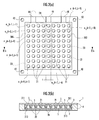
- a nonlinear resistance element 1 according to a first embodiment of the present invention includes a ceramic sheet 2 formed in a sheet shape and a plurality of electrode plates arranged in a separable state on each of a pair of main surfaces of the ceramic sheet 2. 301 to 303, and a pair of insulating pressing plates 4 disposed on the surface of the electrode plates 301 to 303 opposite to the surface in contact with the ceramic sheet 2, respectively.
- the ceramic sheet 2 has a plurality of ceramic pieces (or ceramic beads) 21 made of a ceramic sintered body containing zinc oxide (ZnO) as a main component, and an insulating property that supports each of the ceramic pieces 21 in a separated state. And a support member 22 made of a material. These ceramic pieces 21 have a surface exposed from the surface of the insulating support member 22 and a surface exposed from the back surface of the support member 22. These ceramic pieces 21 are supported by a support member 22 in a state of being spaced apart from each other, and each of these ceramic pieces 21 is an independent non-linear resistance element (also used as a varistor or a capacitor). A plurality of unit areas 23 that can be used as a varistor or the like are formed.
- the ceramic pieces 21 are supported in a state of being separated from each other in the direction parallel to the main surface of the ceramic sheet 2. You may make it contact
- the ceramic piece 21 is not limited to a circular shape, and may be another rectangular shape such as a rectangle or a polygon, an ellipse, a sphere, or an ellipsoid.
- the ceramic sheet 2 is manufactured in the following manner. First, ZnO is a major component, Bi 2 O 3: 0.5mol% , Sb 2 O 3: 1.0mol%, Co 2 O 3: 0.5mol%, MnO 2: 0.5 mol%, Cr 2 Add O 3 : 0.5 mol%, Al (NO 3 ) ⁇ 9H 2 O: 0.01 mol%, add a solvent and a dispersant, mix, and then add a binder to make a slurry, then powder with a spray dryer Create The powder is molded with a mold to obtain a molded body having a diameter of 4.3 mm and a thickness of 1.2 mm. The compact is fired at 1100 ° C. for 2 hours to form a circular ceramic piece 21 having a thickness of 1 m and a diameter of 3.6 mm. Moreover, the ceramic piece 21 is heat-treated as necessary.
- An injection molding method or insert in which a plurality of ceramic pieces 21 obtained in this way are arranged, for example, in a mold so as to be spaced apart from each other and arranged on the same plane, and an insulating resin is injected into a gap between the plurality of ceramic pieces 21
- the ceramic sheet 2 is manufactured by a forming method.
- the ceramic sheet 23 is manufactured by the injection molding method or the insert molding method, but the manufacturing method of the ceramic sheet 2 is not limited to this.
- the ceramic piece 21 and a fluid insulating resin are kneaded and extruded (doctor blade method or extrusion molding method), or the ceramic piece 21 and a resin curable by heat, ultraviolet light, or the like are molded.
- the ceramic sheet 2 may be manufactured by a method in which the resin is hardened.
- the material composition of the ceramic piece 21 is not limited to the Bi 2 O 3 -based nonlinear resistance element 1 in which Bi 2 O 3 is added to zinc oxide as a main component, but is also a Pr 6 O 11 system, a BaTiO 3 system, a SrTiO 3 system.
- a non-linear resistance element 1 of 3 system, TiO 2 system, SnO 2 system or Fe 3 O 4 system may be used.
- the ceramic piece 21 is described as being made of a sintered body containing zinc oxide as a main component.
- non-linear electrical resistance characteristics such as strontium titanate, silicon carbide, and tin oxide are provided. Any ceramic may be used.
- the support member 22 to which the ceramic piece 21 is bonded by using a resin material excellent in flame retardancy, heat resistance and thermal conductivity, it is possible to improve thermal properties and electrical performance. It is effective not only to select the resin material itself, but also to add various additives for improving flame retardancy, heat resistance and thermal conductivity. For example, oxides such as alumina, aluminum nitride and boron nitride, non-oxide additions, particles obtained by insulating the surface of thermally conductive particles (whether metal or non-metal compounds), and in some cases conductive particles You may make it add in a trace amount in the range which does not fall insulation.
- the electrode plates 301 to 303 are made of a flat metal plate made of a conductor such as copper, brass or aluminum, and the terminal portion 31 for electrical connection with a wiring board or the like is a main body portion of the electrode plates 301 to 303. It is extended integrally from.
- the terminal portion 31 for example, the non-linear resistance element can be easily mounted on a wiring board or the like.
- a region surrounded by a two-dot chain line indicates electrode plates 301 to 303 arranged on the upper main surface of the ceramic sheet 2.
- a region surrounded by a broken line indicates a unit area 23 that is defined differently for each embodiment. Here, only the arrangement mode of the unit areas 23 on the upper main surface of the ceramic sheet 2 shown in FIG. 1 is shown.
- two electrode plates 301 and 302 are arranged on the upper main surface of the ceramic sheet 2, and one electrode plate 303 is arranged on the lower main surface.
- the ceramic piece 21 of the ceramic sheet 2 and the electrode plates 301 to 303 may be electrically connected with the conductive resin 5 interposed therebetween. Thereby, even if some gaps are generated on the front and back surfaces of the individual ceramic sheets 2 during production, the ceramic pieces 21 and the electrode plates 301 to 303 can be reliably conducted.
- the conductive resin 5 is formed by applying and drying a conductive paste containing silver particles and a thermoplastic resin on one or both surfaces of the ceramic piece 21 or the ceramic sheet 2.
- a conductive paste containing silver particles and a thermoplastic resin As the material composition of the conductive resin 5, it is possible to use a room temperature curable conductive adhesive containing silver as conductive particles, or a thermosetting conductive adhesive.
- the conductive particles can be copper, gold, carbon, or the like.
- the pressing plate 4 is formed in a flat plate shape having a larger surface area than the ceramic sheet 2 and the electrode plates 301 to 303.
- the male screw portion 41 is screwed into a female screw portion 42 formed on one side of the presser plate 4. That is, by tightening the male screw portion 41, the ceramic sheet 2 and the electrode plates 301 to 303 are fixed while being sandwiched between the presser plates 4. Then, by loosening the male screw portion 41, the ceramic sheet 2 and the electrode plates 301 to 303 are separated from the presser plate 4, respectively.
- the ceramic sheet 2 or the electrode plates 301 to 303 of the nonlinear resistance element body can be easily replaced. Therefore, the maintainability of the non-linear resistance element can be improved.
- the electrical characteristics such as the varistor voltage and the energy tolerance may be required to be changed depending on the specifications of the lightning arrester and surge absorber.
- the conventional non-linear resistance element in which the electrode plate and the ceramic sintered body (ceramic sheet) are soldered, a plurality of non-linear resistance elements are prepared and connected in series or in parallel, and the varistor voltage, energy A measure to adjust the tolerance is considered.
- such a measure secures a space for mounting a plurality of new non-linear resistance elements, and in some cases, it is necessary to change the design of the wiring board. Therefore, the electrical characteristics of the non-linear resistance elements can be changed. It was difficult.
- the ceramic sheet 2 and the electrode plates 301 to 303 are not joined by soldering or the like unlike the conventional nonlinear resistive element.
- the ceramic sheet 2 and the electrode plates 301 to 303 can be separated and replaced. For this reason, the electrical characteristic of the non-linear resistance element 1 can be changed easily.
- a single ceramic sheet 2 having a plurality of ceramic pieces 21 as a constituent element can constitute a plurality of nonlinear resistance elements 1 having different electrical characteristics.
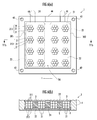
- a region surrounded by a broken line indicates a unit area 23 that is defined differently for each embodiment.
- a region surrounded by a two-dot chain line indicates electrode plates 311 to 314 disposed on the upper main surface of the ceramic sheet 2.
- three electrode plates 311 to 313 are disposed on the upper main surface of the ceramic sheet 2, and two electrode plates 314 are disposed on the lower main surface. And 315 are arranged.
- three unit areas 23 including the three groups of ceramic pieces 21 are defined on the upper main surface of the ceramic sheet 2 (see the broken line in FIG. 3A).
- two unit areas 23 including each of the two groups of the ceramic pieces 21 are defined on the lower main surface of the ceramic sheet 2.
- four electrode plates 321 to 324 are arranged on the upper main surface of the ceramic sheet 2, and two electrodes are arranged on the lower main surface. Plates 325 and 326 are disposed.
- two unit areas 23 including the two groups of ceramic pieces 21 are defined on the upper main surface of the ceramic sheet 2 (see the broken line in FIG. 3C).
- two unit areas 23 including each of the two groups of the ceramic pieces 21 are defined on the lower main surface of the ceramic sheet 2.
- the holding plate 4 has a receiving portion 43 into which the main body portions of the ceramic sheet 2 and the electrode plates 301 to 303 are fitted, and a guide groove in which the terminal portions 31 of the electrode plates 301 to 303 are guided to the outside of the holding plate 4. 44 is formed.
- the presser plate 4 is made of a transparent member such as acrylic resin. Accordingly, the size, shape, and the like of the ceramic sheet 2 and the electrode plates 301 to 303 in use can be confirmed in a state where the nonlinear resistance element 1 is assembled without being disassembled.
- the switching means for switching between the sandwiched state and the separated state of the ceramic sheet 2 and the electrode plates 301 to 303 is not limited to the male screw portion 41 and the female screw portion 42.
- the holding state of the ceramic sheet 2 and the electrode plates 301 to 303 may be fixed by sandwiching both ends of the holding plate 4 with a clip or the like.
- a claw portion may be provided on one presser plate, and the other presser plate may be hooked and fixed using the elasticity of the material.
- the nonlinear resistance element 1 in the second to fifth embodiments is different only in the configuration of the ceramic piece 21 arranged in the unit area 23 in the first embodiment.
- the ceramic piece 21 according to the second embodiment of the present invention is formed in a columnar shape, and is exposed from the surface 211 exposed from the surface of the insulating support member 22 and from the back surface of the support member 22. It has a surface 212.
- the unit area 23 consists of the several ceramic piece 21 with respect to the one unit area 23, and these ceramic pieces 21 are contact
- the ceramic piece 21 according to the third embodiment of the present invention is formed in a flat plate shape, and is exposed from the surface 211 exposed from the surface of the insulating support member 22 and from the back surface of the support member 22. It has a surface 212.
- the unit area 23 consists of the one ceramic piece 21 with respect to the one unit area 23, and the unit area 23 has only two places.
- the ceramic piece 21 in the fourth embodiment of the present invention is formed in a spherical shape and constitutes a plurality of ceramic piece groups 213 that are in contact with each other in the horizontal direction and the thickness direction of the ceramic sheet 2. ing.
- These ceramic piece groups 213 respectively constitute a plurality of conduction paths penetrating in the thickness direction of the ceramic sheet, and these conduction paths are formed by a surface 211 partially protruding from the surface of the support member 22 and the support member 22.
- a surface 212 partially protrudes from the back surface.
- the unit area 23 is composed of a plurality of ceramic piece groups 213 with respect to one unit area 23, and is arranged on the same plane of the ceramic sheet 2 with an insulating support member 22 therebetween.
- the ceramic piece 21 according to the fifth embodiment of the present invention is formed in a spherical shape, a surface 211 protruding from the surface of the insulating support member 22, and a surface protruding from the back surface of the support member 22. 212.
- the unit area 23 is composed of a plurality of ceramic pieces 21 with respect to one unit area 23, and is arranged on the same plane of the ceramic sheet 2 so as to be separated from each other via an insulating support member 22.
- the support member 22 in the fifth embodiment of the present invention is made of an insulating resin excellent in flexibility that can be bent elastically in addition to flame retardancy, heat resistance, and thermal conductivity.
- a synthetic resin such as urethane elastomer or olefin elastomer.
- the ceramic sheet 2 according to the fifth embodiment of the present invention can be bent by the elastic force of the support member 22, so that the electrode plates 301 to 303 are formed to be greatly curved as shown in FIG. Even if it is made, it can be deformed along the surfaces of the electrode plates 301 to 303, and the protruding portion of the ceramic piece 21 can be brought into contact with the electrode plates 301 to 303 reliably.
- the unit area 23 is divided by the boundary region 24 formed of the insulating support member 22. Therefore, when the plurality of electrode plates 301 to 303 are arranged on the same plane in accordance with the arrangement pattern of the plurality of unit areas 23, short-circuiting of these electrode plates 301 to 303 is prevented, which is the same as in the first embodiment. Similarly, the distance t between these electrode plates 301 to 303 is reduced.
- the ceramic sheet 2 and the electrode plates 301 to 303 can be separated and removed depending on the holding plate 4 as in the first embodiment. It is possible. Thereby, even when it is desired to change the electrical characteristics of the nonlinear resistance element 1 or when the performance of the ceramic sheet 2 is deteriorated, the ceramic sheet 2 or the electrode plates 301 to 303 of the nonlinear resistance element body can be easily replaced. It is possible to do it. For example, when the ceramic sheet 3 breaks down, a new ceramic sheet 2 may be replaced, or a ceramic sheet 2 having a different form as shown in another embodiment may be replaced.
- the nonlinear resistance element 1 can be easily changed and assembled can be obtained.
- the ceramic pieces 21 are regularly arranged, but may be irregularly arranged.
- the shape of the ceramic sheet 2 is not limited to a rectangular shape, and may be arbitrarily changed according to its use, such as a circular shape.
- SYMBOLS 1 Nonlinear resistance element 1, 2 ... Ceramic sheet, 21 ... Ceramic piece, 23 ... Unit area, 24 ... Boundary area, 301-303 ... Electrode plate, 4 ... Holding plate.
Landscapes
- Engineering & Computer Science (AREA)
- Microelectronics & Electronic Packaging (AREA)
- Physics & Mathematics (AREA)
- Electromagnetism (AREA)
- Thermistors And Varistors (AREA)
- Connection Of Batteries Or Terminals (AREA)
Abstract
複数の電極間の間隔の狭小化を図ることが可能な非線形抵抗素子を提供する。 非線形抵抗素子を構成する複数のセラミックスシート21が、絶縁性素材から成る支持部材22によりシート状に支持されることにより構成されている。複数のセラミックスピース21が、相互に離間している複数のユニットエリア23のそれぞれに区分されて配置されている。
Description
本発明は非線形抵抗素子に関し、例えば、避雷器、サージ吸収素子、電圧安定化素子などを組み込んだ電気機器に用いられ、雷サージ、開閉サージなどの異常電圧から電気機器を保護する非線形抵抗素子に関する。
一般的にバリスタと称される非線形抵抗素子は、印加電圧によってその抵抗値が変化する特性、つまり、正常な電圧が印加された時には高抵抗値であって絶縁特性を示し、異常な高電圧が印加された時には低抵抗値を示す非直線性の電圧-電流特性を具備する。このような特性を有するバリスタは、サージやノイズの吸収を目的とした避雷器やサージ吸収器、あるいは電圧安定化素子に広く利用されている。
この非線形抵抗素子は、例えば、主成分の酸化亜鉛に非直線性の電圧-電流特性を発現させる基本添加物である酸化ビスマス、酸化アンチモン、酸化コバルトと、さらに性能向上のために添加される各種の酸化物とを含む酸化亜鉛原料粉末を成形して焼成させたセラミック焼結体からなる。
このセラミック焼結体の表面及び裏面には、銀ペーストを焼き付け処理による下地導電層が形成され、その下地導電層の上に、銅、黄銅やアルミなどの導電体からなる金属製の電極板が半田付けにより複数接合される。そして、このセラミック焼結体及び電極板を含む主要部をエポキシ樹脂などでモールドすることにより、そのモールド部から電極部材の端子部を導出した非線形抵抗素子が製品化されている(例えば、特許文献1参照)。
ところで、導電体からなる金属製の電極板は、一体的に焼成されたセラミックス焼結体と比べて熱膨張率が大きい。そのため、従来の非線形抵抗素子では、電極板を半田付け又はバリスタ使用時の熱応力によりセラミック焼結体にクラックが生じ破損するおそれがある。また、シート状に形成されたセラミックス焼結体は外力に対して脆いので、輸送又は実装時などにより発生する外力によっても破損するおそれがある。このような問題を回避するために、従来の非線形抵抗素子では、セラミック焼結体の板厚を厚く形成して剛性を高める対策が行われていた。
一方で、セラミック焼結体上に接合された複数の電極板は、電極板間の短絡を防ぐために、電極板間の間隔をセラミック焼結体の板厚の2倍以上にする必要がある。しかしながら、従来の非線形抵抗素子では、セラミック焼結体が板厚を厚く形成する必要があるため、電極板間の間隔が広大化し、この結果、非線形抵抗素子全体が大型化する。そうすると、大型化した非線形抵抗素子では、配線基板上の狭小スペースへの実装が困難になるという点で問題があった。
そこで、本発明は、上記問題点に鑑み、複数の電極間の間隔の狭小化を図ることが可能な非線形抵抗素子を提供し、非線形抵抗素子の構成全体のコンパクト化を図ることを目的とする。
本発明の非線形抵抗素子は、セラミックス焼結体から成る複数のセラミックスピースと、複数の前記セラミックスピースのそれぞれを支持する絶縁性素材から成るシート状の支持部材とで構成されたセラミックスシートを少なくとも備え、一又は複数の前記セラミックスピースが前記セラミックスシートをその厚み方向に貫通する複数の導通経路のそれぞれを構成し、かつ、前記導通経路の両端を構成する前記セラミックスピースが前記支持部材から部分的に露出している非線形抵抗素子であって、複数の前記セラミックスピースが、相互に離間している複数のユニットエリアのそれぞれに区分されて配置されている状態で、複数の前記セラミックスピースのそれぞれが前記支持部材により支持されていることを特徴とする。
本発明の非線形抵抗素子によれば、複数のセラミックスピースにより形成された導電経路の両端が支持部材から露出し、かつ、複数のセラミックスピースが相互に離間しているユニットエリアごとに区分して配置されている。すなわち、絶縁性の支持部材のうち異なるユニットエリア間の境界領域又は中間領域を構成する部分により、当該異なるユニットエリアのそれぞれに配置されている一又は複数のセラミックスピースが絶縁されている。
このため、複数のユニットエリアの配置パターンにしたがって、複数の導電体又は電極が各ユニットエリアに配置されているセラミックスピースとの電気的接点を有するように配置された場合であっても、当該複数の導電体又は電極が短絡することが防止されうる。これに加えて、セラミックスシートがバルクのセラミック焼結体により構成されている先行技術と比較して、当該複数の導電体又は電極の間隔の狭小化が図られる。したがって、その分だけ、複数のユニットエリアの間隔の狭小化が図られ、セラミックスシート、ひいては当該セラミックスシート及び当該複数の導電体又は電極を構成要素とする非線形抵抗素子(バリスタ、又は、コンデンサ兼用のバリスタなど)のコンパクト化が図られる。
本発明の非線形抵抗素子において、前記セラミックスシートの一対の主面のうち一方又は両方において、複数の前記ユニットエリアのそれぞれに配置されている単一又は複数の前記セラミックスピースと電気的に導通し、かつ、前記支持部材のうち異なる前記ユニットエリア間の境界領域を挟んで相互に離間している状態で配設される複数の電極板を備えていることが好ましい。
当該構成の非線形抵抗素子によれば、複数のユニットエリアが、絶縁性の境界領域によりそれぞれ独立した非線形抵抗素子(バリスタ、又は、コンデンサ兼用バリスタなど)として利用可能に区分されている。このため、電極板の大きさ又は形状等が変更されている場合、電極板の変更前後で異なる電気的特性を有する非線形抵抗素子が得られる。例えば、表面積が大きい電極板に変更されると、電極板と接触するユニットエリアの表面積が増大し、エネルギー耐量の大きい非線形抵抗素子が得られる。
これにより、非線形抵抗素子の全体構成としてのコンパクト化を図りながらも、電極板の変更により非線形抵抗素子の電気的特性の変更が容易に行うことができる。
また、本発明の非線形抵抗素子は、前記セラミックスシートの一対の主面のそれぞれに前記電極板が配設されているものにおいて、前記電極板の前記セラミックスシートに接触する面とは反対側の面にそれぞれ配設される一対の絶縁性の押え板と、複数の前記電極板がそれぞれ対応する複数の前記ユニットエリアに配置されたセラミックスピースと電気的に導通し、かつ、前記セラミックスシートとその一対の主面のそれぞれに当接する一対の前記電極板と前記押え板の間に挟持されている挟持状態と、前記押え板から前記セラミックスシートとその一対の主面のそれぞれに当接する一対の前記電極板とが分離する分離状態とを切り換える切換手段とを備えていることが好ましい。
当該構成の非線形抵抗素子によれば、セラミックスシートとその一対の主面のそれぞれに当接する一対の電極板とが、一対の押え板の間に挟持された挟持状態と、セラミックスシートとその一対の主面のそれぞれに当接する一対の電極板とが押え板から分離した分離状態とを切り換えること切換手段(締付ねじ、クリップなど)を有している。すなわち、従来の非線形抵抗素子のように、セラミックスシート及び電極板が半田付け等により接合されていないため、セラミックスシートと電極板とを分離して取り外すことが可能となっている。
このため、例えば、セラミックスシートの性能が低下した場合は、セラミックスシートの交換を容易に行うことができる。また、非線形抵抗素子の電気的特性を変更したい場合も、電極板を交換することが容易に行うことができる。これにより、非線形抵抗素子の保守性の向上が図られる。
(本発明の第1実施形態)
まずは、本発明に係る非線形抵抗素子の第1の実施形態について、図1及び図2を参照しながら説明する。
本発明の第1の実施形態の非線形抵抗素子1は、シート状に形成されたセラミックスシート2と、セラミックスシート2の一対の主面のそれぞれに分離可能な状態で配設された複数の電極板301~303と、電極板301~303のセラミックスシート2に接触する面とは反対側の面にそれぞれ配設された一対の絶縁性の押え板4とで構成されている。
まずは、本発明に係る非線形抵抗素子の第1の実施形態について、図1及び図2を参照しながら説明する。
本発明の第1の実施形態の非線形抵抗素子1は、シート状に形成されたセラミックスシート2と、セラミックスシート2の一対の主面のそれぞれに分離可能な状態で配設された複数の電極板301~303と、電極板301~303のセラミックスシート2に接触する面とは反対側の面にそれぞれ配設された一対の絶縁性の押え板4とで構成されている。
セラミックスシート2は、酸化亜鉛(ZnO)を主成分とするセラミックス焼結体から成る複数のセラミックスピース(又はセラミックスビーズ)21と、これらのセラミックスピース21のそれぞれを離間させた状態で支持する絶縁性素材から成る支持部材22とで構成されている。これらのセラミックスピース21は、絶縁性の支持部材22の表面から露出する面と、支持部材22の裏面から露出する面を有している。また、これらのセラミックスピース21は、相互に離間して配置させた状態で支持部材22により支持されており、これらの個々のセラミックスピース21は、それぞれ独立した非線形抵抗素子(バリスタ、又は、コンデンサ兼用バリスタなど)として利用可能な複数のユニットエリア23を形成している。
なお、第1の実施形態では、セラミックスピース21は、セラミックシート2の主面に並行な方向について、それぞれを離間させた状態で支持されているが、同一のユニットエリア23内であれば、それぞれ当接させても良い。また、セラミックスピース21は、円形に限定されるものではなく、長方形、多角形などその他の角形、楕円形、球形又は楕円球形などであってもよい。
また、セラミックスシート2は、以下の要領でもって製作される。まず、主成分であるZnOに、Bi2O3:0.5mol%、Sb2O3:1.0mol%、Co2O3:0.5mol%、MnO2:0.5 mol%、Cr2O3:0.5mol%、Al(NO3)・9H2O:0.01mol%を添加して溶剤および分散剤を加えて混合した後、バインダを加えてスラリーを製作しスプレードライヤーで粉体を作成する。その粉体を金型で成形し、直径4.3mm、厚み1.2mmの成形体を得る。その成形体を1100℃で2時間焼成して厚み1mで直径3.6mmの円形のセラミックスピース21を形成する。また、必要に応じてセラミックスピース21を熱処理する。
このようにして得られた複数のセラミックスピース21を、例えば、金型内に相互に離間して同一平面上に並べて、複数のセラミックスピース21の隙間に絶縁性樹脂を注入する射出成形法又はインサート成形法によってセラミックスシート2を製作する。
なお、上記では、射出成形法又はインサート成形法によりセラミックスシート23が製作されると説明しているが、セラミックスシート2の製作方法はこれに限定されない。例えば、セラミックスピース21と流動性がある状態の絶縁性樹脂とを混練して押出す方法(ドクターブレード法や押出成形法)、若しくは、セラミックスピース21と熱や紫外線等で硬化する樹脂とを型に嵌めて樹脂を硬化する方法により、セラミックスシート2を製作してもよい。
また、セラミックスピース21の材料組成としては、主成分である酸化亜鉛にBi2O3を添加したBi2O3系の非線形抵抗素子1に限らず、Pr6O11系、BaTiO3系、SrTiO3系、TiO2系、SnO2系やFe3O4系の非線形抵抗素子1であってもよい。また、上記実施形態では、セラミックスピース21が酸化亜鉛を主成分とする焼結体からなると説明しているが、例えば、チタン酸ストロンチウム、炭化ケイ素、酸化スズなどの非直線性の電気抵抗特性を有するセラミックスであれば良い。
また、セラミックスピース21を接着する支持部材22としては、難燃性、耐熱性や熱伝導性に優れた樹脂材料を用いることにより、熱的性質の向上や電気性能の改善を図ることができる。この樹脂材料そのものの選択だけに限らず、難燃性、耐熱性や熱伝導性を改善するための各種添加物を添加することも有効である。例えば、アルミナ、窒化アルミニウム、窒化ホウ素などの酸化物、非酸化物の添加や、熱伝導性粒子(金属あるいは非金属化合物を問わない)の表面を絶縁加工した粒子、場合によっては導電性粒子を絶縁性が低下しない範囲で微量添加するようにしてもよい。
電極板301~303は、銅、黄銅やアルミなどの導電体からなる金属製の平坦な板材からなり、配線基板などと電気的に接続するための端子部31が電極板301~303の本体部から一体的に延設されている。この端子部31を利用することにより、例えば、非線形抵抗素子が配線基板などへ実装が容易になる。
図2において、二点鎖線で囲まれた領域は、セラミックスシート2の当該上側の主面に配設される電極板301~303を示している。また、図2において、破線で囲まれた領域は、実施例ごとに異なって定義されているユニットエリア23を示している。ここでは、図1に示されているセラミックスシート2の上側の主面におけるユニットエリア23の配置態様のみが示されている。
9行9列に配置されているセラミックスピース21のそれぞれが、9次の正方行列の要素{aij(i=1~9,j=1~9)}により区別されていると考える。
図2に示されている実施例によれば、セラミックスシート2の上側の主面には2つの電極板301及び302が配置され、下側の主面には1つの電極板303が配置される。当該上側の2つの電極板301及び302のそれぞれが当接するセラミックスピース21の組み合わせは、2つの群(aij(i=1~9,j=1~4))及び(aij(i=1~9,j=6~9))のそれぞれにより表される。
すなわち、この場合、セラミックスシート2の上側の主面においては、セラミックスピース21の当該2つの群を包含する2つのユニットエリア23が定義される(図2破線参照)。一方、当該下側の電極板303は、全てセラミックスピース21の群(aij(i=1~9,j=1~9))となっている。
電極板301→セラミックスピース21の群(aij(i=1~9,j=1~4))→電極板303→セラミックスピース21の群(aij(i=1~9,j=6~9))→電極板302という一連の電気導通経路を構成する非線形抵抗素子1が得られる。
また、電極板301及び302は、それぞれに相当するユニットエリア23の間に配置された、セラミックスピース21の群(aij(i=1~9,j=5))が含まれる境界領域24に存在する絶縁性素材によって短絡が防止されている。これにより、セラミックスシート2の上側の主面に配設された電極板301及び302の間隔tの狭小化が図られる。
なお、セラミックスシート2のセラミックスピース21と電極板301~303とは、導電性樹脂5を介在させて導通するようにしても良い。これにより、製造時に個々のセラミックスシート2の表面及び裏面に多少ギャップが発生しても、セラミックスピース21と電極板301~303を確実に導通させることができる。
導電性樹脂5は、セラミックスピース21又はセラミックスシート2の一方あるいは両方の面に銀粒子と熱可塑性樹脂を含む導電ペーストを塗布および乾燥させて形成される。導電性樹脂5の材料組成としては、導電粒子としての銀を含む常温硬化型導電性接着剤やそれ以外に熱硬化型の導電性接着剤を使用することが可能である。さらに、導電粒子としては銀以外にも、銅や金あるいはカーボン等を用いることが可能である。
押え板4は、セラミックスシート2及び電極板301~303よりも大きい表面積を有する平板状に形成されている。また、押え板4の四隅には、セラミックスシート2及び電極板301~303が押え板の間に狭持された狭持状態と、押え板からセラミックスシート及び電極板が分離する分離状態とを切り換えるための雄ねじ部41(切換手段)を有している。この雄ねじ部41は、押え板4の一方に形成された雌ねじ部42に螺合される。すなわち、雄ねじ部41を締め付けることにより、セラミックスシート2及び電極板301~303が押え板4の間に挟持された状態で固定される。そして、雄ねじ部41を緩めることにより、押え板4からセラミックスシート2及び電極板301~303がそれぞれ分離される。
これにより、非線形抵抗素子1の電気的特性を変更したい場合、又は、セラミックスシート2の性能が低下した場合であっても、非線形抵抗素子本体のセラミックスシート2又は電極板301~303の交換が容易に行うことができるので、非線形抵抗素子の保守性の向上が図られる。
例えば、避雷器やサージ吸収器の仕様用途によって、バリスタ電圧、エネルギー耐量等の電気的特性の変更が要求されることがある。このような場合、従来の電極板とセラミック焼結体(セラミックスシート)が半田付けされた非線形抵抗素子では、複数の非線形抵抗素子を用意しこれらを直列又は並列に接続して、バリスタ電圧、エネルギー耐量等を調整するという対策が考えられる。しかしながら、このような対策は、新たな複数の非線形抵抗素子を実装するスペースを確保し、場合によっては、配線基板の設計変更が必要となるため、非線形抵抗素子の電気的特性を変更することが困難であった。
これに対し、本発明に係る第1実施形態の非線形抵抗素子1によれば、従来の非線形抵抗素子のように、セラミックスシート2及び電極板301~303が半田付け等により接合されていないため、セラミックスシート2と電極板301~303とを分離して取り替えることが可能となっている。このため、非線形抵抗素子1の電気的特性を容易に変更することができる。
各電極板301~303と、当該各電極板301~303と当接するセラミックスピース21が含まれている各ユニットエリア23とのそれぞれの面積、形状及び配置態様のうち少なくとも1つが変更されることにより、複数のセラミックスピース21を構成要素とする単一のセラミックスシート2により、複数の異なる電気特性を有する非線形抵抗素子1が構成されうる。
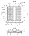
電気特性の異なる非線形抵抗素子1の構成の実施例について、図3を参照しながら説明する。図3(a)~(c)のそれぞれの右側において、破線で囲まれた領域は、実施例ごとに異なって定義されているユニットエリア23を示している。ここでは、図3(a)~(c)のそれぞれの左側に示されているセラミックスシート2の上側の主面におけるユニットエリア23の配置態様のみが示されている。また、図3(a)~(c)のそれぞれの右側において、二点鎖線で囲まれた領域は、セラミックスシート2の当該上側の主面に配設される電極板311~314を示している。
9行9列に配置されているセラミックスピース21のそれぞれが、9次の正方行列の要素{aij(i=1~9,j=1~9)}により区別されていると考える。
図3(a)左側に示されている実施例によれば、セラミックスシート2の上側の主面には3つの電極板311~313が配置され、下側の主面には2つの電極板314及び315が配置される。当該上側の3つの電極板311~313のそれぞれが当接するセラミックスピース21の組み合わせは、3つの群(aij(i=1~4,j=1~4))、(aij(i=1~4,j=6~9))及びaij(i=6~9,j=1~9)のそれぞれにより表される。当該下側の2つの電極板314及び315のそれぞれが当接するセラミックスピース21の組み合わせは、2つの群(aij(i=1~9,j=1~4))及びaij(i=1~9,j=6~9)のそれぞれである。
すなわち、この場合、セラミックスシート2の上側の主面においては、セラミックスピース21の当該3つの群を包含する3つのユニットエリア23が定義される(図3(a)破線参照)。その一方、セラミックスシート2の下側の主面においては、セラミックスピース21の当該2つの群のそれぞれを包含する2つのユニットエリア23が定義される。
電極板311→セラミックスピース21の群(aij(i=1~4,j=1~4))→電極板314→セラミックスピース21の群(aij(i=6~9,j=1~4))→電極板313→セラミックスピース21の群(aij(i=6~9,j=6~9))→電極板315→セラミックスピース21の群(aij(i=1~4,j=6~9))→電極板312という一連の電気導通経路を構成する、バリスタ電圧の大きい非線形抵抗素子1が得られる。
また、電極板311及び312は、それぞれに相当するユニットエリア23の間に配置された、セラミックスピース21の群(aij(i=1~4,j=5))が含まれる境界領域24に存在する絶縁性素材によって短絡が防止されている。電極板311及び313、312及び313、並びに314及び315も同様に短絡が防止されている。これにより、第1の実施形態と同様に、当該電極板の間隔tの狭小化が図られる。
また、図3(b)左側に示されている実施例によれば、セラミックスシート2の上側の主面には4つの電極板321~324が配置され、下側の主面には2つの電極板325及び326が配置される。当該上側の4つの電極板321~324のそれぞれが当接するセラミックスピース21の組み合わせは、4つの群(aij(i=1~4,j=1~4))、(aij(i=1~4,j=6~9))、(aij(i=6~9,j=1~4))及びaij(i=6~9,j=6~9)のそれぞれにより表される。当該下側の2つの電極板325及び326のそれぞれが当接するセラミックスピース21の組み合わせは、2つの群(aij(i=1~4,j=1~9))及びaij(i=6~9,j=1~9)のそれぞれである。
すなわち、この場合、セラミックスシート2の上側の主面においては、セラミックスピース21の当該4つの群を包含する4つのユニットエリア23が定義される(図3(b)破線参照)。その一方、セラミックスシート2の下側の主面においては、セラミックスピース21の当該2つの群のそれぞれを包含する2つのユニットエリア23が定義される。
非線形抵抗素子1が、2つの別個の非線形抵抗素子として構成される。すなわち、電極板321→セラミックスピース21の群(aij(i=1~4,j=1~4))→電極板325→セラミックスピース21の群(aij(i=6~9,j=1~4))→電極板322という一連の電気導通経路と、電極板323→セラミックスピース21の群(aij(i=6~9,j=1~4))→電極板326→セラミックスピース21の群(aij(i=6~9,j=6~9))→電極板324という一連の電気導通経路とのそれぞれにより構成される2つの非線形抵抗素子が構成される。
また、電極板321及び322は、それぞれに相当するユニットエリア23の間に配置された、セラミックスピース21の群(aij(i=1~4,j=5))が含まれる境界領域24に存在する絶縁性素材によって短絡が防止されている。電極板321及び323、322及び324、323及び324、並びに325及び326も同様に短絡が防止されている。これにより、第1の実施形態と同様に、当該電極板の間隔tの狭小化が図られる。
また、図3(c)左側に示されている実施例によれば、セラミックスシート2の上側の主面には2つの電極板331及び332が配置され、下側の主面には2つの電極板333及び334が配置される。当該上側の2つの電極板331及び332のそれぞれが当接するセラミックスピース21の組み合わせは、2つの群(aij(i=1~9,j=1~4))及びaij(i=1~9,j=6~9)のそれぞれにより表される。当該下側の2つの電極板333及び334のそれぞれが当接するセラミックスピース21の組み合わせは、2つの群(aij(i=1~9,j=1~4))及びaij(i=1~9,j=6~9)のそれぞれである。
また、図3(c)左側に示されている実施例によれば、セラミックスシート2の上側の主面には2つの電極板331及び332が配置され、下側の主面には2つの電極板333及び334が配置される。当該上側の2つの電極板331及び332のそれぞれが当接するセラミックスピース21の組み合わせは、2つの群(aij(i=1~9,j=1~4))及びaij(i=1~9,j=6~9)のそれぞれにより表される。当該下側の2つの電極板333及び334のそれぞれが当接するセラミックスピース21の組み合わせは、2つの群(aij(i=1~9,j=1~4))及びaij(i=1~9,j=6~9)のそれぞれである。
すなわち、この場合、セラミックスシート2の上側の主面においては、セラミックスピース21の当該2つの群を包含する2つのユニットエリア23が定義される(図3(c)破線参照)。その一方、セラミックスシート2の下側の主面においては、セラミックスピース21の当該2つの群のそれぞれを包含する2つのユニットエリア23が定義される。
非線形抵抗素子1が、2つの別個の非線形抵抗素子として構成される。すなわち、電極板331→セラミックスピース21の群(aij(i=1~9,j=1~4))→電極板333という一連の電気導通経路と、電極板332→セラミックスピース21の群(aij(i=6~9,j=1~4))→電極板334という一連の電気導通経路とのそれぞれにより構成される2つの非線形抵抗素子が構成される。
また、電極板331及び332は、それぞれに相当するユニットエリア23の間に配置された、セラミックスピース21の群(aij(i=1~9,j=5))が含まれる境界領域24に存在する絶縁性素材によって短絡が防止されている。電極板333及び334も同様に短絡が防止されている。これにより、第1の実施形態と同様に、当該電極板の間隔tの狭小化が図られる。
また、押え板4には、セラミックスシート2及び電極板301~303の本体部が嵌めこまれる受け部43と、電極板301~303の端子部31が押え板4の外側へ案内される案内溝44とが形成されている。これにより、セラミックスシート2及び電極板301~303を押え板4の間に挟みこむ際に、セラミックスシート2及び電極板301~303が所定位置に位置決めされるため、非線形抵抗素子1の組立作業が容易になる。
さらに、押え板4は、アクリル樹脂等の透明部材から成ることが望ましい。これにより、非線形抵抗素子1を分解せずに組み立てられた状態で、使用中のセラミックスシート2及び電極板301~303の大きさ、形状等を確認することができる。
なお、セラミックスシート2及び電極板301~303の挟持状態と分離状態とを切り換える切換手段は、雄ねじ部41及び雌ねじ部42に限定されない。例えば、押え板4の両端をクリップのようなもので挟んで、セラミックスシート2及び電極板301~303の挟持状態を固定しても良い。また、いわゆるスナップフィットのように、一方の押え板に爪部を設け、材料の弾性を利用して他方の押え板を引っ掛けて固定しても良い。
(本発明の他の実施形態)
次に、本発明に係る非線形抵抗素子の第2から5の実施形態について、図4から図7を参照しながら、以下に詳述する。
次に、本発明に係る非線形抵抗素子の第2から5の実施形態について、図4から図7を参照しながら、以下に詳述する。
なお、図1及び2に示した構成と同様の構成については同一の符号を付して説明を省略する。第2から5の実施形態における非線形抵抗素子1は、上記第1実施形態におけるユニットエリア23に配置されたセラミックスピース21の構成のみが相違する。
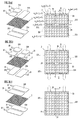
本発明の第2の実施形態におけるセラミックスピース21は、図4に示すように、円柱状に形成され、絶縁性の支持部材22の表面から露出する面211と、支持部材22の裏面から露出する面212を有している。そして、ユニットエリア23は、一のユニットエリア23に対し複数のセラミックスピース21から成り、これらのセラミックスピース21が互いに導通可能に当接されている。
本発明の第3の実施形態におけるセラミックスピース21は、図5に示すように、平板状に形成され、絶縁性の支持部材22の表面から露出する面211と、支持部材22の裏面から露出する面212を有している。そして、ユニットエリア23は、一のユニットエリア23に対し一のセラミックスピース21から成り、ユニットエリア23は二箇所のみとなっている。
本発明の第4の実施形態におけるセラミックスピース21は、図6に示すように、球状に形成され、セラミックスシート2の水平方向及び厚み方向にそれぞれ相互に当接する複数のセラミックピース群213を構成している。これらのセラミックスピース群213は、セラミックスシートの厚み方向に貫通する複数の導通経路をそれぞれ構成し、これらの導通経路は、支持部材22の表面から部分的に突出する面211と、支持部材22の裏面から部分的に突出する面212を有している。そして、ユニットエリア23は、一のユニットエリア23に対し複数のセラミックピース群213から成り、セラミックスシート2の同一平面上に絶縁性の支持部材22を介して相互に離間して並べられている。
本発明の第5の実施形態におけるセラミックスピース21は、図7に示すように、球状に形成され、絶縁性の支持部材22の表面から突出する面211と、支持部材22の裏面から突出する面212を有している。そして、ユニットエリア23は、一のユニットエリア23に対し複数のセラミックスピース21から成り、セラミックスシート2の同一平面上に絶縁性の支持部材22を介して相互に離間して並べられている。
また、本発明の第5の実施形態における支持部材22は、難燃性、耐熱性や熱伝導性に加えて、弾性的に撓み得る可撓性に優れた絶縁性樹脂から構成されている。例えば、ウレタン系エラストマーやオレフィン系エラストマーなどの合成樹脂から成るものであることが望ましい。
これにより、本発明の第5の実施形態におけるセラミックスシート2は、支持部材22の弾性力によって撓ませることができるので、図7に示すように、電極板301~303が大きく湾曲するように形成されていても、この電極板301~303の表面に沿うように変形させ、セラミックスピース21の突出部分を当該電極板301~303に対して確実に当接させることができる。
これらの図5から7に示す第2から5の実施形態は、何れも、ユニットエリア23が絶縁性の支持部材22から成る境界領域24によって区分されている。このため、複数の電極板301~303が複数のユニットエリア23の配置パターンにしたがって同一平面上に配設された場合、これらの電極板301~303の短絡が防止され、第1の実施形態と同様に、これらの電極板301~303の間隔tの狭小化が図られる。
また、これらの図5から7に示す第2から5の実施形態は、第1実施形態と同様に、押え板4によっては、セラミックスシート2と電極板301~303とを分離して取り外すことが可能となっている。
これにより、非線形抵抗素子1の電気的特性を変更したい場合、又は、セラミックスシート2の性能が低下した場合であっても、非線形抵抗素子本体のセラミックスシート2又は電極板301~303の交換が容易に行うことが可能となっている。例えば、セラミックスシート3が故障等した場合、新しいセラミックスシート2を取り替えても良く、他の実施形態に示す形態が異なるセラミックスシート2に取り替えても良い。また、従来のように一体的に焼成されたセラミック焼結体から成るセラミックスシート2に取り替えても良く、このような場合であっても、図8に示す第6の実施形態ように、電極板301~303の単端子と多端子の交換等が容易に行えるので、非線形抵抗素子1の変更及び組み立てが容易に行えるという本発明の効果を得ることができる。
これにより、非線形抵抗素子1の電気的特性を変更したい場合、又は、セラミックスシート2の性能が低下した場合であっても、非線形抵抗素子本体のセラミックスシート2又は電極板301~303の交換が容易に行うことが可能となっている。例えば、セラミックスシート3が故障等した場合、新しいセラミックスシート2を取り替えても良く、他の実施形態に示す形態が異なるセラミックスシート2に取り替えても良い。また、従来のように一体的に焼成されたセラミック焼結体から成るセラミックスシート2に取り替えても良く、このような場合であっても、図8に示す第6の実施形態ように、電極板301~303の単端子と多端子の交換等が容易に行えるので、非線形抵抗素子1の変更及び組み立てが容易に行えるという本発明の効果を得ることができる。
以上、本発明の実施形態について図面を参照して説明したが、本発明はこれに限定されない。例えば、図1から7に示す上記第1から5の実施形態では、セラミックスピース21が規則的に配置されているが、不規則的に配置されていてもよい。セラミックスシート2の形状は、矩形状に限らず、円形状等、その用途に合わせて任意に変更されうる。
1‥非線形抵抗素子1、2‥セラミックスシート、21‥セラミックスピース、 23‥ユニットエリア、24‥境界領域、301~303‥電極板、4‥押え板。
Claims (3)
- セラミックス焼結体から成る複数のセラミックスピースと、複数の前記セラミックスピースのそれぞれを支持する絶縁性素材から成るシート状の支持部材とで構成されたセラミックスシートを少なくとも備え、
一又は複数の前記セラミックスピースが前記セラミックスシートをその厚み方向に貫通する複数の導通経路のそれぞれを構成し、かつ、前記導通経路の両端を構成する前記セラミックスピースが前記支持部材から部分的に露出している非線形抵抗素子であって、
複数の前記セラミックスピースが、相互に離間している複数のユニットエリアのそれぞれに区分されて配置されている状態で、複数の前記セラミックスピースのそれぞれが前記支持部材により支持されていることを特徴とする非線形抵抗素子。 - 請求項1記載の非線形抵抗素子において、
前記セラミックスシートの一対の主面のうち一方又は両方において、複数の前記ユニットエリアのそれぞれに配置されている単一又は複数の前記セラミックスピースと電気的に導通し、かつ、前記支持部材のうち異なる前記ユニットエリア間の境界領域を挟んで相互に離間している状態で配設される複数の電極板を備えていることを特徴とする非線形抵抗素子。 - 請求項2記載の非線形抵抗素子において、前記セラミックスシートの一対の主面のそれぞれに前記電極板が配設されているものにおいて、
前記電極板の前記セラミックスシートに接触する面とは反対側の面にそれぞれ配設される一対の絶縁性の押え板と
複数の前記電極板がそれぞれ対応する複数の前記ユニットエリアに配置されたセラミックスピースと電気的に導通し、かつ、前記セラミックスシートとその一対の主面のそれぞれに当接する一対の前記電極板と前記押え板の間に挟持されている挟持状態と、前記押え板から前記セラミックスシートとその一対の主面のそれぞれに当接する一対の前記電極板とが分離する分離状態とを切り換える切換手段とを備えることを特徴とする非線形抵抗素子。
Priority Applications (4)
| Application Number | Priority Date | Filing Date | Title |
|---|---|---|---|
| EP13772928.1A EP2704158B1 (en) | 2012-04-04 | 2013-03-28 | Nonlinear resistive element |
| KR1020137031796A KR20140140475A (ko) | 2012-04-04 | 2013-03-28 | 비선형 저항 소자 |
| CN201380001516.1A CN103563014B (zh) | 2012-04-04 | 2013-03-28 | 非线性电阻元件 |
| US14/119,989 US8902039B2 (en) | 2012-04-04 | 2013-03-28 | Non-linear resistive element |
Applications Claiming Priority (2)
| Application Number | Priority Date | Filing Date | Title |
|---|---|---|---|
| JP2012-085966 | 2012-04-04 | ||
| JP2012085966A JP5998329B2 (ja) | 2012-04-04 | 2012-04-04 | 非線形抵抗素子 |
Publications (1)
| Publication Number | Publication Date |
|---|---|
| WO2013150953A1 true WO2013150953A1 (ja) | 2013-10-10 |
Family
ID=49300443
Family Applications (1)
| Application Number | Title | Priority Date | Filing Date |
|---|---|---|---|
| PCT/JP2013/059245 WO2013150953A1 (ja) | 2012-04-04 | 2013-03-28 | 非線形抵抗素子 |
Country Status (6)
| Country | Link |
|---|---|
| US (1) | US8902039B2 (ja) |
| EP (1) | EP2704158B1 (ja) |
| JP (1) | JP5998329B2 (ja) |
| KR (1) | KR20140140475A (ja) |
| CN (1) | CN103563014B (ja) |
| WO (1) | WO2013150953A1 (ja) |
Families Citing this family (11)
| Publication number | Priority date | Publication date | Assignee | Title |
|---|---|---|---|---|
| JP5998328B2 (ja) | 2012-04-04 | 2016-09-28 | 音羽電機工業株式会社 | 非線形抵抗素子 |
| TWI600354B (zh) * | 2014-09-03 | 2017-09-21 | 光頡科技股份有限公司 | 具高彎折力之微電阻結構及其製造方法 |
| US10083781B2 (en) | 2015-10-30 | 2018-09-25 | Vishay Dale Electronics, Llc | Surface mount resistors and methods of manufacturing same |
| WO2017075842A1 (zh) * | 2015-11-05 | 2017-05-11 | 隆科电子(惠阳)有限公司 | 一种通过紧固件固定的mov元器件结构 |
| CN105469915A (zh) * | 2015-11-05 | 2016-04-06 | 隆科电子(惠阳)有限公司 | 一种通过紧固件固定的mov元器件结构 |
| CN105304243A (zh) * | 2015-11-12 | 2016-02-03 | 郑品章 | 压敏电阻 |
| CN106782957B (zh) * | 2017-01-17 | 2019-05-17 | 隆科电子(惠阳)有限公司 | 一种具有放电结构的复合型mov组件 |
| US10438729B2 (en) | 2017-11-10 | 2019-10-08 | Vishay Dale Electronics, Llc | Resistor with upper surface heat dissipation |
| KR102139772B1 (ko) * | 2018-11-27 | 2020-07-31 | 삼성전기주식회사 | 바리스터 및 바리스터 제조 방법 |
| US11545284B2 (en) * | 2019-01-16 | 2023-01-03 | Panasonic Intellectual Property Management Co., Ltd. | Varistor assembly |
| TWI687944B (zh) * | 2019-08-15 | 2020-03-11 | 聚鼎科技股份有限公司 | 正溫度係數元件 |
Citations (5)
| Publication number | Priority date | Publication date | Assignee | Title |
|---|---|---|---|---|
| JPS60211801A (ja) * | 1984-04-05 | 1985-10-24 | 松下電器産業株式会社 | バリスタ |
| JPH0262005A (ja) * | 1988-08-29 | 1990-03-01 | Matsushita Electric Ind Co Ltd | シート状バリスタ |
| JP2004006519A (ja) | 2002-05-31 | 2004-01-08 | Otowa Denki Kogyo Kk | 多端子バリスタ |
| JP2008218749A (ja) * | 2007-03-05 | 2008-09-18 | Toshiba Corp | ZnOバリスター粉末 |
| WO2012046765A1 (ja) * | 2010-10-05 | 2012-04-12 | 音羽電機工業株式会社 | 非線形抵抗素子及びその製造方法 |
Family Cites Families (9)
| Publication number | Priority date | Publication date | Assignee | Title |
|---|---|---|---|---|
| GB1037822A (en) * | 1961-12-15 | 1966-08-03 | Ass Elect Ind | Improvements relating to non-linear electrical resistance elements |
| NL6901659A (ja) * | 1969-02-01 | 1970-08-04 | ||
| US3648002A (en) | 1970-05-04 | 1972-03-07 | Essex International Inc | Current control apparatus and methods of manufacture |
| US5262754A (en) * | 1992-09-23 | 1993-11-16 | Electromer Corporation | Overvoltage protection element |
| US6055147A (en) * | 1998-06-24 | 2000-04-25 | Current Technology, Inc. | Apparatus for providing independent over-current protection to a plurality of electrical devices and transient-voltage suppression system employing the apparatus |
| US6323751B1 (en) * | 1999-11-19 | 2001-11-27 | General Electric Company | Current limiter device with an electrically conductive composite material and method of manufacturing |
| TW543258B (en) * | 2001-10-08 | 2003-07-21 | Polytronics Technology Corp | Over current protection apparatus and its manufacturing method |
| DE102006033710B4 (de) * | 2006-07-20 | 2013-04-11 | Epcos Ag | Verfahren zur Herstellung einer Widerstandsanordnung |
| DE102007030653B4 (de) | 2007-07-02 | 2017-04-13 | Phoenix Contact Gmbh & Co. Kg | Überspannungsschutzelement |
-
2012
- 2012-04-04 JP JP2012085966A patent/JP5998329B2/ja active Active
-
2013
- 2013-03-28 EP EP13772928.1A patent/EP2704158B1/en active Active
- 2013-03-28 US US14/119,989 patent/US8902039B2/en active Active
- 2013-03-28 KR KR1020137031796A patent/KR20140140475A/ko not_active Application Discontinuation
- 2013-03-28 WO PCT/JP2013/059245 patent/WO2013150953A1/ja active Application Filing
- 2013-03-28 CN CN201380001516.1A patent/CN103563014B/zh active Active
Patent Citations (5)
| Publication number | Priority date | Publication date | Assignee | Title |
|---|---|---|---|---|
| JPS60211801A (ja) * | 1984-04-05 | 1985-10-24 | 松下電器産業株式会社 | バリスタ |
| JPH0262005A (ja) * | 1988-08-29 | 1990-03-01 | Matsushita Electric Ind Co Ltd | シート状バリスタ |
| JP2004006519A (ja) | 2002-05-31 | 2004-01-08 | Otowa Denki Kogyo Kk | 多端子バリスタ |
| JP2008218749A (ja) * | 2007-03-05 | 2008-09-18 | Toshiba Corp | ZnOバリスター粉末 |
| WO2012046765A1 (ja) * | 2010-10-05 | 2012-04-12 | 音羽電機工業株式会社 | 非線形抵抗素子及びその製造方法 |
Non-Patent Citations (1)
| Title |
|---|
| See also references of EP2704158A4 * |
Also Published As
| Publication number | Publication date |
|---|---|
| JP2013219092A (ja) | 2013-10-24 |
| KR20140140475A (ko) | 2014-12-09 |
| US8902039B2 (en) | 2014-12-02 |
| EP2704158A1 (en) | 2014-03-05 |
| US20140085043A1 (en) | 2014-03-27 |
| CN103563014B (zh) | 2017-09-01 |
| JP5998329B2 (ja) | 2016-09-28 |
| CN103563014A (zh) | 2014-02-05 |
| EP2704158B1 (en) | 2016-05-25 |
| EP2704158A4 (en) | 2014-10-22 |
Similar Documents
| Publication | Publication Date | Title |
|---|---|---|
| JP5998329B2 (ja) | 非線形抵抗素子 | |
| JP5640249B2 (ja) | 非線形抵抗素子及びその製造方法 | |
| KR20200118833A (ko) | 에너지 처리 용량이 향상된 케스케이드 바리스터 | |
| KR101813407B1 (ko) | 복합 전자 부품 및 그 실장 기판 | |
| US20220020532A1 (en) | Electrical component having layered structure with improved breakdown performance | |
| JP2004006519A (ja) | 多端子バリスタ | |
| JP5998328B2 (ja) | 非線形抵抗素子 | |
| KR20220034546A (ko) | 전자 부품 | |
| JP5079632B2 (ja) | 静電気保護素子 | |
| KR101468138B1 (ko) | 적층형 칩 소자 | |
| KR100340130B1 (ko) | 정 온도 계수 서미스터와 배리스터 복합소자 및 그 제조방법 | |
| JP2007305934A (ja) | サージ防護デバイス | |
| JP2013182930A (ja) | 積層型複合電子部品 | |
| CN203480967U (zh) | 层叠型ptc热敏电阻 | |
| KR101282912B1 (ko) | 배리스터장치 | |
| JP2004006517A (ja) | 多端子バリスタ | |
| WO2015087573A1 (ja) | 複合電子部品 | |
| JP2007165526A (ja) | チップ形正特性サーミスタ | |
| JP2007184306A (ja) | チップ形正特性サーミスタ |
Legal Events
| Date | Code | Title | Description |
|---|---|---|---|
| WWE | Wipo information: entry into national phase |
Ref document number: 14119989 Country of ref document: US |
|
| 121 | Ep: the epo has been informed by wipo that ep was designated in this application |
Ref document number: 13772928 Country of ref document: EP Kind code of ref document: A1 |
|
| ENP | Entry into the national phase |
Ref document number: 20137031796 Country of ref document: KR Kind code of ref document: A |
|
| NENP | Non-entry into the national phase |
Ref country code: DE |