WO2013129333A1 - 表示装置 - Google Patents
表示装置 Download PDFInfo
- Publication number
- WO2013129333A1 WO2013129333A1 PCT/JP2013/054805 JP2013054805W WO2013129333A1 WO 2013129333 A1 WO2013129333 A1 WO 2013129333A1 JP 2013054805 W JP2013054805 W JP 2013054805W WO 2013129333 A1 WO2013129333 A1 WO 2013129333A1
- Authority
- WO
- WIPO (PCT)
- Prior art keywords
- detection
- period
- signal
- display device
- display
- Prior art date
- Legal status (The legal status is an assumption and is not a legal conclusion. Google has not performed a legal analysis and makes no representation as to the accuracy of the status listed.)
- Ceased
Links
Images





Classifications
-
- G—PHYSICS
- G06—COMPUTING OR CALCULATING; COUNTING
- G06F—ELECTRIC DIGITAL DATA PROCESSING
- G06F3/00—Input arrangements for transferring data to be processed into a form capable of being handled by the computer; Output arrangements for transferring data from processing unit to output unit, e.g. interface arrangements
- G06F3/01—Input arrangements or combined input and output arrangements for interaction between user and computer
- G06F3/03—Arrangements for converting the position or the displacement of a member into a coded form
- G06F3/041—Digitisers, e.g. for touch screens or touch pads, characterised by the transducing means
- G06F3/0412—Digitisers structurally integrated in a display
-
- G—PHYSICS
- G06—COMPUTING OR CALCULATING; COUNTING
- G06F—ELECTRIC DIGITAL DATA PROCESSING
- G06F3/00—Input arrangements for transferring data to be processed into a form capable of being handled by the computer; Output arrangements for transferring data from processing unit to output unit, e.g. interface arrangements
- G06F3/01—Input arrangements or combined input and output arrangements for interaction between user and computer
- G06F3/03—Arrangements for converting the position or the displacement of a member into a coded form
- G06F3/041—Digitisers, e.g. for touch screens or touch pads, characterised by the transducing means
- G06F3/0416—Control or interface arrangements specially adapted for digitisers
- G06F3/0418—Control or interface arrangements specially adapted for digitisers for error correction or compensation, e.g. based on parallax, calibration or alignment
- G06F3/04184—Synchronisation with the driving of the display or the backlighting unit to avoid interferences generated internally
-
- G—PHYSICS
- G09—EDUCATION; CRYPTOGRAPHY; DISPLAY; ADVERTISING; SEALS
- G09G—ARRANGEMENTS OR CIRCUITS FOR CONTROL OF INDICATING DEVICES USING STATIC MEANS TO PRESENT VARIABLE INFORMATION
- G09G3/00—Control arrangements or circuits, of interest only in connection with visual indicators other than cathode-ray tubes
- G09G3/20—Control arrangements or circuits, of interest only in connection with visual indicators other than cathode-ray tubes for presentation of an assembly of a number of characters, e.g. a page, by composing the assembly by combination of individual elements arranged in a matrix no fixed position being assigned to or needed to be assigned to the individual characters or partial characters
- G09G3/34—Control arrangements or circuits, of interest only in connection with visual indicators other than cathode-ray tubes for presentation of an assembly of a number of characters, e.g. a page, by composing the assembly by combination of individual elements arranged in a matrix no fixed position being assigned to or needed to be assigned to the individual characters or partial characters by control of light from an independent source
- G09G3/36—Control arrangements or circuits, of interest only in connection with visual indicators other than cathode-ray tubes for presentation of an assembly of a number of characters, e.g. a page, by composing the assembly by combination of individual elements arranged in a matrix no fixed position being assigned to or needed to be assigned to the individual characters or partial characters by control of light from an independent source using liquid crystals
- G09G3/3611—Control of matrices with row and column drivers
- G09G3/3614—Control of polarity reversal in general
-
- G—PHYSICS
- G09—EDUCATION; CRYPTOGRAPHY; DISPLAY; ADVERTISING; SEALS
- G09G—ARRANGEMENTS OR CIRCUITS FOR CONTROL OF INDICATING DEVICES USING STATIC MEANS TO PRESENT VARIABLE INFORMATION
- G09G3/00—Control arrangements or circuits, of interest only in connection with visual indicators other than cathode-ray tubes
- G09G3/20—Control arrangements or circuits, of interest only in connection with visual indicators other than cathode-ray tubes for presentation of an assembly of a number of characters, e.g. a page, by composing the assembly by combination of individual elements arranged in a matrix no fixed position being assigned to or needed to be assigned to the individual characters or partial characters
- G09G3/34—Control arrangements or circuits, of interest only in connection with visual indicators other than cathode-ray tubes for presentation of an assembly of a number of characters, e.g. a page, by composing the assembly by combination of individual elements arranged in a matrix no fixed position being assigned to or needed to be assigned to the individual characters or partial characters by control of light from an independent source
- G09G3/36—Control arrangements or circuits, of interest only in connection with visual indicators other than cathode-ray tubes for presentation of an assembly of a number of characters, e.g. a page, by composing the assembly by combination of individual elements arranged in a matrix no fixed position being assigned to or needed to be assigned to the individual characters or partial characters by control of light from an independent source using liquid crystals
- G09G3/3611—Control of matrices with row and column drivers
- G09G3/3648—Control of matrices with row and column drivers using an active matrix
-
- G—PHYSICS
- G09—EDUCATION; CRYPTOGRAPHY; DISPLAY; ADVERTISING; SEALS
- G09G—ARRANGEMENTS OR CIRCUITS FOR CONTROL OF INDICATING DEVICES USING STATIC MEANS TO PRESENT VARIABLE INFORMATION
- G09G3/00—Control arrangements or circuits, of interest only in connection with visual indicators other than cathode-ray tubes
- G09G3/20—Control arrangements or circuits, of interest only in connection with visual indicators other than cathode-ray tubes for presentation of an assembly of a number of characters, e.g. a page, by composing the assembly by combination of individual elements arranged in a matrix no fixed position being assigned to or needed to be assigned to the individual characters or partial characters
- G09G3/34—Control arrangements or circuits, of interest only in connection with visual indicators other than cathode-ray tubes for presentation of an assembly of a number of characters, e.g. a page, by composing the assembly by combination of individual elements arranged in a matrix no fixed position being assigned to or needed to be assigned to the individual characters or partial characters by control of light from an independent source
- G09G3/36—Control arrangements or circuits, of interest only in connection with visual indicators other than cathode-ray tubes for presentation of an assembly of a number of characters, e.g. a page, by composing the assembly by combination of individual elements arranged in a matrix no fixed position being assigned to or needed to be assigned to the individual characters or partial characters by control of light from an independent source using liquid crystals
- G09G3/3611—Control of matrices with row and column drivers
- G09G3/3696—Generation of voltages supplied to electrode drivers
-
- G—PHYSICS
- G06—COMPUTING OR CALCULATING; COUNTING
- G06F—ELECTRIC DIGITAL DATA PROCESSING
- G06F3/00—Input arrangements for transferring data to be processed into a form capable of being handled by the computer; Output arrangements for transferring data from processing unit to output unit, e.g. interface arrangements
- G06F3/01—Input arrangements or combined input and output arrangements for interaction between user and computer
- G06F3/03—Arrangements for converting the position or the displacement of a member into a coded form
- G06F3/041—Digitisers, e.g. for touch screens or touch pads, characterised by the transducing means
- G06F3/044—Digitisers, e.g. for touch screens or touch pads, characterised by the transducing means by capacitive means
Definitions
- the present invention relates to a display device that displays an image.
- display devices including an input device in which a display driving device that displays an image and an input detection device that detects a user's contact (or approach) operation to the display driving device have been widely used.
- a display device is generally manufactured by separately manufacturing a touch panel included in the input detection device and a display panel included in the display driving device, and overlaying the touch panel on the display panel.
- Patent Document 1 discloses a technique for synchronizing the touch screen controller and the display by providing timing information to a touch screen controller (input detection device) from a display driving circuit that drives the display panel. .
- Patent Document 2 all or a part of the plurality of drive electrodes are continuously scanned within a period in which the display screen is displayed a predetermined number of times by display scanning drive that scans and drives the plurality of drive electrodes.
- a technique for performing detection scanning driving to be performed for a display screen more than a predetermined number of times is disclosed.
- Japanese Patent Publication Japanese Patent Laid-Open No. 2010-108501 (published May 13, 2010)” Japanese Patent Publication “Japanese Unexamined Patent Publication No. 2011-13760 (published on January 20, 2011)”
- the display device including the input detection device as described above has a problem that the detection accuracy in the input detection device cannot be sufficiently obtained due to noise generated in the display driving device.
- the display device is a liquid crystal display device
- noise often occurs when the liquid crystal included in the display drive device is driven.
- noise is generated when a voltage corresponding to image data is applied to a pixel in order to display an image on the display driving device.
- the inventor found that a period with less noise due to driving of the liquid crystal is present in addition to the blanking period.
- the present invention has been made on the basis of the inventor's knowledge in order to solve the above-mentioned problems, and its main object is to secure a longer detection period and to obtain a high detection accuracy. Is to provide.
- a display device includes a display driving device that displays an image, and an input detection device that detects an approach or contact of an object to the display driving device.
- a display device wherein the display driving device is connected to each of a plurality of scanning lines, a plurality of image signal lines arranged to intersect the plurality of scanning lines, and the plurality of image signal lines.
- a display panel including a pixel electrode and a common electrode disposed to face each of the pixel electrodes; a scanning line driving circuit for sequentially supplying a scanning signal to the plurality of scanning lines; and the plurality of image signal lines.
- a signal line driving circuit for sequentially supplying image signals to the common electrode, and a constant voltage is applied to the common electrode at least during a scanning period in which the scanning signal is supplied to the scanning line.
- a detection panel for detecting approach or contact the detection panel being arranged along the display panel, wherein the detection panel starts supplying scanning signals to the m-th (m is a natural number) scanning line; From the period until the supply of the scanning signal to the (m + 1) th scanning line starts, the approach of the object in the detectable period that is a period excluding the rising period of the image signal supplied to the image signal line Alternatively, contact detection is performed.
- the display device can secure a longer detection period in order to detect an input operation on the detection panel, thereby obtaining high detection accuracy.
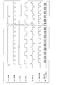
- 6 is a timing chart illustrating the timing of detection processing when the driving method of the display device according to the embodiment of the present invention is a one-dot inversion driving method.
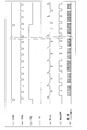
- 6 is a timing chart showing the timing of detection processing when the display device driving method according to an embodiment of the present invention is a one-column inversion driving method. It is a block diagram which shows the outline of the whole structure of the display apparatus which concerns on other embodiment of this invention. It is a timing chart which shows the timing of a detection process in case the drive system of the display apparatus which concerns on further another embodiment of this invention is a 1 dot inversion drive system.
- 4 is a graph showing characteristics of a TFT using an oxide semiconductor, a TFT using a-Si, and a TFT using LTPS in the display device according to each embodiment of the present invention.
- FIG. 1 is a block diagram showing an outline of the overall configuration of the display device 1 according to the present embodiment.
- the display device 1 includes a display drive device 10, an input detection device 20, and a system-side control unit 30.
- the display driving device 10 includes a display panel 11, a scanning line driving circuit 12, a signal line driving circuit 13, a common electrode driving circuit 14, a timing control unit (control means) 15, and a power supply circuit 16. ing.
- an active matrix type liquid crystal display device is employed as the display driving device 10. Therefore, the display panel 11 of the present embodiment is an active matrix type liquid crystal display panel, and the other components described above are for driving the liquid crystal display panel.
- the display panel 11 includes a plurality of gate signal lines (scanning lines) G and a plurality of source signal lines (image signal lines) S, and is defined by the gate signal lines G and the source signal lines S.
- a plurality of pixels (pixel regions) are provided. Note that the plurality of pixels are arranged in a so-called lattice pattern including a plurality of pixel columns and a plurality of pixel rows.
- the display panel 11 is provided with a total of N source signal lines S and a total of M gate signal lines G, and M rows ⁇ N columns (M and N are natural numbers). A plurality of pixels are provided.
- the nth source signal line is S (n)
- the mth gate signal line is G (m) (m and n are natural numbers satisfying m ⁇ M and n ⁇ N, respectively).
- the display panel 11 includes, for each pixel region, the pixel electrode and the pixel electrode by a gate electrode supplied to the pixel electrode, the common electrode disposed to face the pixel electrode, and the gate signal line G.
- TFT switching element
- the plurality of gate signal lines G are juxtaposed in the pixel column direction (direction along the pixel column). Each of the plurality of gate signal lines G is electrically connected to each pixel of the corresponding pixel row of the plurality of pixel rows.
- the plurality of source signal lines S are juxtaposed in the pixel row direction (the direction along the pixel rows), and all are orthogonal to each of the plurality of gate signal lines G.
- Each of the plurality of source signal lines S is electrically connected to each pixel of the corresponding pixel column of the plurality of pixel columns.
- the gate signal line G supplies the gate signal supplied from the scanning line driving circuit 12 to the connected TFT.
- the source signal line S supplies the source signal supplied from the signal line driver circuit 13 to the pixel electrode through the connected TFT.
- the display panel is a liquid crystal display panel
- the present invention is not limited to this, and may be, for example, an EL display or a plasma display. .
- the scanning line driving circuit 12 sequentially selects and scans the plurality of gate signal lines G. Specifically, the scanning line driving circuit 12 sequentially selects a plurality of gate signal lines G, and with respect to the selected gate signal line G, switching elements (TFTs) provided in each pixel on the gate signal line G. ) Is supplied with a scanning signal having an on-voltage for switching on.
- TFTs switching elements
- the signal line drive circuit 13 While the gate signal line G is selected, the signal line drive circuit 13 supplies a source signal corresponding to the image data from the corresponding source signal line S to each pixel on the gate signal line G. More specifically, the signal line drive circuit 13 calculates the value of the voltage to be output to each pixel on the selected gate signal line G based on the input image signal, and uses the voltage of that value as a source. Output from the output amplifier toward each source signal line S. As a result, a source signal is supplied to each pixel on the selected gate signal line G, and the source signal is written.
- the common electrode drive circuit 14 supplies a predetermined common voltage for driving the common electrode to the common electrode provided in each of the plurality of pixels.
- the timing control unit 15 is a control unit that controls the scanning line driving circuit 12, the signal line driving circuit 13, and the common electrode driving circuit 14.
- the image signal and the control signal are input to the timing control unit 15 from the system control unit 30.
- the image signal includes a clock signal, a synchronization signal, an image data signal, and the like.
- the image may be a moving image or a still image.
- the timing control unit 15 outputs various control signals for operating each driving circuit in synchronization with each driving circuit.
- the timing control unit 15 supplies a gate start pulse signal, a gate clock signal GCK, and a gate output control signal GOE to the scanning line driving circuit 12.
- the scanning line driving circuit 12 starts scanning the plurality of gate signal lines G. Then, the scanning line driving circuit 12 sequentially supplies an ON voltage to each gate signal line G in accordance with the gate clock signal GCK and the gate output control signal GOE.
- the timing control unit 15 outputs a source start pulse signal, a source latch strobe signal, and a source clock signal to the signal line driving circuit 13. Based on the source start pulse signal, the signal line drive circuit 13 stores the input image data of each pixel in a register according to the source clock signal, and the image data for each source signal line S according to the next source latch strobe signal. The source signal corresponding to the is supplied.
- the timing control unit 15 can switch the driving method of the display device 1 by switching the driving method of the display driving device 10, and can control the scanning line driving circuit 12 and the signal line driving circuit 13 according to the switched driving method. preferable.
- a driving method in addition to a normal driving method, for example, a dot inversion driving method for inverting the polarity of a scanning signal supplied to the gate signal line G every i (i is a natural number) rows, and a source signal line S
- a column inversion driving method of inverting the curve of the source signal supplied to each j (j is a natural number) column can be mentioned, but is not limited thereto.
- a line inversion driving method, an interlace driving method, and the like can be given.
- any driving method switched by the timing control unit 15 is a polarity inversion driving method.
- the display driving device 10 can be driven using the polarity inversion driving method, high detection accuracy can be obtained while reducing the burn-in of the display panel 11.
- the display driving apparatus 10 further includes a detection synchronization signal generation unit (synchronization signal supply unit) 151.
- a detection synchronization signal generation unit 151 as one function of the timing control unit 15.
- the detection synchronization signal generation unit 151 generates a detection synchronization signal (synchronization signal) that indicates the timing of detection processing when detecting a user input operation in the detection unit 21 described later.
- the detection synchronization signal generation unit 151 generates a detection synchronization signal according to the driving method switched by the timing control unit 15. The detection synchronization signal will be described later.
- the detection synchronization signal generation unit 151 outputs polarity inversion information indicating the polarity inversion of the source signal supplied from the timing control unit 15 to the signal line drive circuit 13 to the detection unit control unit 22. May be.
- the power supply circuit 16 supplies a voltage to each of the scanning line driving circuit 12, the signal line driving circuit 13, and the common electrode driving circuit 14, as indicated by a dotted arrow in FIG. To do.
- the input detection device 20 includes a detection unit (detection panel) 21 and a detection unit control unit 22.
- the configuration of the detection unit 21 will be described with reference to FIG.
- FIG. 2 is a diagram schematically illustrating the configuration of the detection unit 21.
- the detection unit 21 is a unit that detects the approach or contact of an object (for example, a finger or a touch pen) (hereinafter also referred to as a detection process), and is disposed along the display panel 11 provided in the display driving device 10, for example. This is realized by a touch panel.
- a detection process for example, a touch panel.
- the detection unit 21 is, for example, a capacitive touch panel will be described as an example.
- the detection unit 21 includes a plurality of drive lines D and a plurality of sense lines C, and the plurality of drive lines D and the plurality of sense lines C are provided so as to be orthogonal to each other. ing.
- the detection unit 21 is provided with a total number of P drive lines D and a total number of Q sense lines C (P and Q are natural numbers).
- the pth drive line is D (p)
- the qth sense line is C (q) (p and q are natural numbers satisfying p ⁇ P and q ⁇ Q, respectively).
- the drive line D is sequentially supplied with a detection pulse signal from the first drive line D (1) to the Pth drive line D (P). Further, when the detection pulse signal is supplied to the drive line D, the value of the capacitance of the sense line C changes when the user's finger or touch pen touches or approaches the detection unit 21. The detection unit 21 detects the approach or contact of the object by outputting the changed capacitance value of the sense line C.
- the detection unit control unit 22 controls the timing of detection processing in the detection unit 21. For example, the detection unit control unit 22 starts the supply of the scanning signal to the m-th gate signal line G (m) constituting the display panel 11 included in the display driving device 10, and then the m + 1-th gate signal line G. In the period until the supply of the scanning signal at (m + 1), the detection unit 21 detects the contact of the object in the period excluding the rising period of the image signal supplied to each source signal line S. Control timing.
- the detection unit control unit 22 acquires a detection synchronization signal from the timing control unit 15 included in the display driving device 10 as indicated by a thick arrow in FIG.
- the detection unit control unit 22 determines the timing for supplying the detection pulse signal to the detection unit 21 based on the acquired detection synchronization signal, and also determines the number of pulses included in the supplied pulse signal.
- the detection unit control unit 22 sequentially supplies the detection pulse signal determined based on the detection synchronization signal to each drive line D included in the detection unit 21. In this way, the detection unit control unit 22 performs contact detection of an object by the detection unit 21 based on the detection synchronization signal supplied from the display driving device 10.
- the detection unit control unit 22 acquires a change in the capacitance value of the sense line C output from the detection unit 21.
- the detection unit control unit 22 detects a user input operation in the detection unit 21 based on the obtained change in the capacitance value of the sense line C.
- the detection unit control unit 22 supplies detection data indicating the detected user input operation to the system-side control unit 30.
- the system-side control unit 30 outputs an image signal and a control signal to the timing control unit 15 included in the display driving device 10. Further, the system-side control unit 30 acquires detection data supplied from the detection unit control unit 22. The system-side control unit 30 controls each unit of the display device 1 based on the acquired detection data.
- the display panel 11 and the detection unit 21 that is a detection panel are formed in close contact with each other so that air does not enter (an air layer is not formed). According to this, the thickness of the display device 1 in the direction in which the display panel 11 and the detection unit 21 overlap can be reduced.
- the display panel 11 and the detection unit 21 that is a detection panel may be integrally formed. According to this, the thickness of the display device 1 in the direction in which the display panel 11 and the detection unit 21 overlap can be further reduced. Moreover, since it is not necessary to provide the display panel 11 and the detection part 21 separately, the number of parts of the display apparatus 1 can be reduced, and thereby cost can be reduced.
- FIG. 3 is a graph showing a measurement result of noise generated in each horizontal synchronization period in the display panel 11.
- 3A shows noise during the first to third horizontal synchronization periods (1H to 3H) in the xth frame (x is a natural number), and
- FIG. 3B shows the first to third frames in the x + 1th frame. Noise during the third horizontal synchronization period (1H to 3H) is shown.
- Vsync indicates a frame start signal for notifying the start of each frame
- GOE indicates a period of horizontal synchronization (H sync)
- Noise indicates a display panel. No. 11 shows noise generated.
- Hsync and GCK can be cited in addition to GOE.
- a period including a scanning period for scanning each gate signal line (corresponding to a period in which DOE is at a high level) and a horizontal blanking period (corresponding to a period in which DOE is at a low level) are horizontal.
- the supply of the source signal to the source signal line S is started simultaneously with the start of the first horizontal synchronization period.
- noise is generated immediately after the start of the first horizontal synchronization period, that is, immediately after the start of supply of the source signal to the source signal line S. It becomes smaller (stable).
- noise is generated immediately after the start of the second horizontal synchronization period, and the noise is stabilized after a certain period.
- noise is generated immediately after the start of the third horizontal synchronization period, and the noise is stabilized after a certain period.
- the period from the start of each horizontal synchronization period to the elapse of a certain period corresponds to the rising or falling period of the source signal supplied to the source signal line S.
- the rising period and the falling period of the source signal may not be distinguished from each other and both may be expressed as a “rising period”.
- the period from the start of the first horizontal synchronization period to the stabilization of the noise is 9.0 ⁇ s.
- the period from the start of the second horizontal synchronization period to the stabilization of noise is 7.6 ⁇ s
- the period from the start of the third horizontal synchronization period to the stabilization of noise is 9.0 ⁇ s.
- the period from the start of the first horizontal synchronization period to the occurrence of noise is 1.8 ⁇ s.
- the period from the start of the second horizontal synchronization period to the occurrence of noise is 0.4 ⁇ s, and the period from the start of the third horizontal synchronization period to the occurrence of noise is 1.8 ⁇ s.
- the supply of the source signal to the source signal line S is started simultaneously with the start of the first horizontal synchronization period.
- noise occurs immediately after the start of the first horizontal synchronization period, that is, immediately after the start of supply of the source signal to the source signal line S. It becomes smaller (stable).
- noise is generated immediately after the start of the second horizontal synchronization period, and the noise is stabilized after a certain period.
- noise is generated immediately after the start of the third horizontal synchronization period, and the noise is stabilized after a certain period.
- the period during which the noise is large is small.
- the inventor has found that there is a (stable) period.
- the reason why the period of high noise and the period of low noise exist in the horizontal synchronization period is that the potential of the source signal line S fluctuates greatly (ie, the pixel electrode) due to the start of supply of the source signal to the source signal line S.
- the potential of the source electrode line S fluctuates greatly, and noise is generated. Thereafter, the variation in the potential of the source signal line S is small (that is, the variation in the potential of the pixel electrode is small) until the supply of the source signal is terminated. This is because it becomes small and stable.
- Non-detection period a period in which the noise is large (a rising period of the source signal supplied to the source signal line S) during the horizontal synchronization period, from the start of the horizontal synchronization period until the noise becomes stable, is referred to as a non-detection period. To do.
- the time constant ⁇ is on the order of several ⁇ s (it also changes depending on the panel size and resolution).
- each horizontal synchronization period in the n frame and the n + 1 frame does not significantly affect the period until the noise is stabilized, whereas each horizontal synchronization period is an odd period (1H in FIG. 3). 3H) or an even period (2H in FIG. 3), the period until the noise becomes stable may be different.
- a non-detection period is set for each of the different periods until the noise becomes stable (in FIG. 3, two non-detection periods are set). It is preferable to set a period.
- the detection synchronization signal generation unit 151 the period during which the noise is stable during the horizontal synchronization period (that is, the period excluding the non-detection period) and the detection in the detection unit 21 A detection synchronization signal is generated to synchronize with the period for processing.
- the detection synchronization signal is a signal for instructing the timing of detection processing when detecting a user input operation in the detection unit 21 according to the driving method of the display device 1 switched by the timing control unit 15.
- the input detection device 20 acquires the detection synchronization signal generated by the detection synchronization signal generation unit 151 included in the display driving device 10, and performs detection processing by the detection unit 21 at the timing indicated by the detection synchronization signal.
- the detection synchronization signal is a non-detection period in a period from when the supply of the scanning signal to a certain gate signal line G is started until the operation signal is supplied to the next gate signal line G of the certain gate signal line G.
- the signal is preferably a signal indicating the start timing of the detectable period, which is a period excluding “”, and more preferably a signal indicating the start timing to the end timing of the detectable period (that is, the detectable period itself).
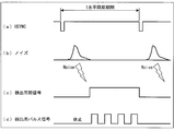
- FIG. 4 is a timing chart showing the detection synchronization signal generated in the detection synchronization signal generation unit 151 according to this embodiment.
- This noise is caused by, for example, the rise of the source signal supplied to the source signal line S as described above.
- the detection synchronization signal generating unit 151 generates a detection synchronization signal during one horizontal synchronization period and after the non-detection period shown in (b) has elapsed, as shown in FIG.
- the generated detection synchronization signal is supplied to the detection unit control unit 22 included in the input detection device 20.
- the detection unit control unit 22 generates a detection pulse signal as shown in (d) of FIG. 4 based on the supplied detection synchronization signal.
- the detection unit 21 can perform detection processing during a period in which the influence of noise generated in the display driving device 10 is small, and thus high detection accuracy can be obtained.
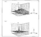
- FIG. 5 is a graph showing the detection accuracy of the user input operation in the detection unit 21.
- 5A shows the detection accuracy when the display driving device 10 and the input detection device 20 are not synchronized by the detection synchronization signal
- FIG. 5B shows the detection accuracy when the synchronization is performed.
- the x-axis and the y-axis indicate the position in the detection unit 21, and the z-axis indicates the change in capacitance of the detection unit 21 detected by the detection unit 21, respectively. Yes.
- the detection synchronization signal synchronizes the image display operation in the display drive device 10 and the input operation detection operation in the input detection device 20 (that is, in the detection unit 21 in the horizontal synchronization period excluding the non-detection period).
- the detection process is performed), as shown in FIG. 5B, only the change A can be detected efficiently. become.
- the non-detection period is from the start of the horizontal synchronization period to the time when noise is stabilized
- the present invention is not limited to this.
- a configuration shown in FIG. 3 in which the period from the start of the first horizontal synchronization period to the occurrence of noise is a period that is not included in the non-detection period (that is, a period for performing detection processing in the detection unit 21). May be.
- frame inversion driving is performed in which the polarity of the source signal supplied to each source signal line S is inverted between the x-th frame and the x + 1-th frame.
- the present invention is not limited to this.
- two-frame inversion driving in which the polarity of the source signal is inverted every two frames
- X-frame inversion driving in which the polarity of the source signal is inverted every X frames (X is a natural number) may be performed.
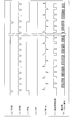
- FIG. 6 is a timing chart showing the timing of detection processing when the driving method of the display device 1 is the one-dot inversion driving method.
- 6A shows a vertical synchronization signal (VSYNC)
- FIG. 6B shows a horizontal synchronization signal (HSYNC)
- FIG. 6C shows a frame polarity signal (FPOL) indicating the polarity of each frame
- FPOL frame polarity signal
- LPOL line polarity signal
- LPOL line polarity signal
- g indicates a detection pulse signal.
- the horizontal synchronization signal includes a frame period (corresponding to a period when VSYNC is at a high level) and a vertical blanking period (corresponding to a period when VSYNC is at a low level).
- the control unit 15 controls the scanning line driving circuit 12 and the signal line driving circuit 13 so as to refresh the image displayed on the display panel 11 in the frame period.
- the frame polarity signal is inverted for each frame period indicated by the vertical synchronization signal, as shown in (a) and (c) of FIG. Further, as shown in FIGS. 6B and 6D, the line polarity signal is inverted every horizontal synchronization period indicated by the horizontal synchronization signal.
- the detection synchronization signal generation unit 151 generates a detection synchronization signal in which the noisy period shown in (e) is a non-detection period. At this time, as shown in FIG. 6 (e), since the absolute values of the noise are substantially the same, each horizontal synchronization is performed during a period when the detection synchronization signal generated by the detection synchronization signal generation unit 151 is at a high level. It becomes substantially constant over the period.
- the timing control unit 15 supplies the detection synchronization signal generated by the detection synchronization signal generation unit 151 to the detection unit control unit 22.
- the detection unit control unit 22 generates a detection pulse signal shown in (g) of FIG. 6 according to the supplied detection synchronization signal, and supplies the generated detection pulse signal to the detection unit 21.
- the detection unit 21 performs detection processing according to the detection pulse signal supplied from the detection unit control unit 22.
- the driving method of the display device 1 is the dot inversion driving method, as shown in FIG. 6F
- the period in which the detection synchronization signal is at a high level is substantially constant in each horizontal synchronization period.
- the timing of the detection process and the length of the period for performing the detection process are substantially constant in each horizontal synchronization period, as shown in (g).
- the detection part 21 can perform a detection process in the period when the influence of the noise which generate
- FIG. 7 is a timing chart showing the timing of detection processing when the driving method of the display device 1 is the one-column inversion driving method.
- 7A shows the vertical synchronization signal (VSYNC),
- VSYNC shows the horizontal synchronization signal (HSYNC),
- FPOL frame polarity signal
- LPOL line polarity signal
- e shows noise
- f shows a detection synchronization signal
- g shows a detection pulse signal.
- the frame polarity signal is inverted every frame period indicated by the vertical synchronization signal, as shown in FIGS. Further, the line polarity signal is constant regardless of the frame period and the horizontal synchronization period indicated by the horizontal synchronization signal, as shown in FIGS.
- the detection synchronization signal generation unit 151 generates a detection synchronization signal in which the noisy period shown in (e) is a non-detection period.
- the period during which the detection synchronization signal generated by the detection synchronization signal generation unit 151 is at a high level is also horizontal. It will be different for each synchronization period.
- the timing control unit 15 supplies the detection synchronization signal generated by the detection synchronization signal generation unit 151 to the detection unit control unit 22.
- the detection unit control unit 22 generates the detection pulse signal shown in (g) of FIG. 7 according to the supplied detection synchronization signal, and supplies the generated detection pulse signal to the detection unit 21.
- the detection unit 21 performs detection processing according to the detection pulse signal supplied from the detection unit control unit 22.
- the driving method of the display device 1 is a column inversion driving method, as shown in (f) of FIG. 7, the period during which the detection synchronization signal is at a high level differs for each horizontal synchronization period. And the length of the period for performing the detection process also differ for each horizontal synchronization period as shown in (g).
- the detection part 21 can perform a detection process in the period when the influence of the noise which generate
- the detection synchronization signal generation unit 151 when the timing control unit 15 switches the driving method of the display device 1, the detection synchronization signal generation unit 151 performs detection processing timing according to the switched driving method. It is possible to generate a detection synchronization signal indicating Therefore, the detection unit 21 can perform detection processing at a timing suitable for the driving method switched by the timing control unit 15.
- the configuration in which the detection synchronization signal generation unit 151 generates the detection synchronization signal according to the driving method of the display device 1 has been described as an example.
- the present invention is not limited to this. Absent.
- the display device 1 includes a storage unit (not shown) that stores a detection synchronization signal corresponding to each driving method in advance, and the detection device 1 is switched by the timing control unit 15.
- a configuration may be employed in which a detection synchronization signal corresponding to the driving method is read from the storage unit.
- the detection synchronization signal is a signal indicating a period during which the detection process in the detection unit 21 can be performed
- the present invention is not limited to this.
- a configuration in which the detection synchronization signal is a signal that indicates the start timing of the detection process in the detection unit 21 may be employed.
- the timing control unit 15 may determine which drive method is the current drive method based on a combination of the line polarity signal and the frame polarity signal. In this case, the timing control unit 15 may generate a detection synchronization signal suitable for the driving method determined by the combination of the line polarity signal and the frame polarity signal.
- the timing control unit 15 can generate a detection synchronization signal suitable for the current driving method even when the current driving method is not recognized. it can.
- FIG. 8 is a diagram showing an overall configuration of the display device 1 according to the present embodiment.
- the display device 2 according to this embodiment is configured so that the detection synchronization signal is input to the system control unit 30 ′ from the detection synchronization signal generation unit 151 ′ included in the timing control unit 15 ′. Except for being supplied from the side control unit 30 ′ to the detection unit control unit 22 ′ included in the input detection device 20 ′, the configuration is the same as that of the display device 1 described in the first embodiment.
- the timing control unit 15 ′ included in the display driving device 10 ′ outputs the detection synchronization signal generated by the detection synchronization signal generation unit 151 ′ to the system-side control unit 30 ′.
- the system-side control unit 30 ′ supplies the detection synchronization signal acquired from the timing control unit 15 ′ to the detection unit control unit 22 ′ included in the input detection device 20 ′.
- the detection unit control unit 22 ′ determines the timing for supplying the detection pulse signal to the detection unit 21 and also determines the number of pulses to be supplied. .
- the system-side control unit 30 ′ detects polarity inversion information indicating polarity inversion of the source signal (video signal) supplied to the signal line drive circuit 13 via the timing control unit 15. You may output to control part 22 '.
- FIGS. 3 Another embodiment of the present invention will be described with reference to FIGS.
- the present embodiment is implemented except that the detection unit control unit 22 has a function of setting a detection period for designating the timing of detection processing in the detection unit 21 regardless of the detection synchronization signal.
- the display device 1 is the same as the display device 1 according to the first embodiment.
- the timing control unit 15 includes the display device 1. The operation of the display device 1 when the driving method is switched between the dot inversion driving method and the column inversion driving method will be described.
- FIG. 9 is a timing chart showing detection processing timing when the driving method of the display device 1 is switched to the one-dot inversion driving method.
- 9A shows the vertical synchronizing signal (VSYNC)
- FIG. 9B shows the horizontal synchronizing signal (HSYNC)
- FIG. 9C shows the frame polarity signal (FPOL)
- FIG. 9D shows the line polarity signal shown.
- (LPOL) shows noise
- (f) shows a detection period indicating the timing of detection processing in the detection unit 21 set by the detection unit control unit 22, and
- (g) shows a detection pulse. The signal is shown.
- the horizontal synchronization signal includes a frame period (corresponding to a period when VSYNC is at a high level) and a vertical blanking period (corresponding to a period when VSYNC is at a low level).
- the control unit 15 controls the scanning line driving circuit 12 and the signal line driving circuit 13 so as to refresh the image displayed on the display panel 11 in the frame period.
- the frame polarity signal is inverted every frame period indicated by the vertical synchronization signal, as shown in FIGS. Further, as shown in FIGS. 9B and 9D, the line polarity signal is inverted every horizontal synchronization period indicated by the horizontal synchronization signal.
- the detection unit control unit 22 sets a detection period in which the noisy period shown in (e) is set as a non-detection period. At this time, as shown in (e) of FIG. 9, since the absolute values of the noise are substantially the same, the high level in the period (f) of FIG. 9 is set as the detection period by the detection unit control unit 22. Corresponding to the period of time) becomes substantially constant in each horizontal synchronization period.
- the detection unit control unit 22 generates a detection pulse signal shown in (g) of FIG. 9 according to the set detection period, and supplies the generated detection pulse signal to the detection unit 21.
- the detection unit 21 performs detection processing according to the detection pulse signal supplied from the detection unit control unit 22.
- the detection period is substantially constant in each horizontal synchronization period.
- the length of the period during which processing is performed is substantially constant in each horizontal synchronization period.
- the detection unit 21 can perform detection processing in a period in which the influence of noise generated in the display driving device 10 is small according to the detection period set by the detection unit control unit 22, so that high detection accuracy is achieved. Obtainable.
- FIG. 10 is a timing chart showing the timing of detection processing when the driving method of the display device 1 is switched to the one-column inversion driving method.
- 10A shows the vertical synchronization signal (VSYNC)
- FIG. 10B shows the horizontal synchronization signal (HSYNC)
- FIG. 10C shows the frame polarity signal (FPOL)
- FIG. 10D shows the line polarity signal (HPOL).
- LPOL line polarity signal
- (e) shows noise
- (f) shows a detection period indicating the timing of detection processing in the detection unit 21 set by the detection unit control unit 22, and
- g shows a detection pulse signal. Is shown.
- the frame polarity signal is inverted every frame period indicated by the vertical synchronization signal, as shown in FIGS. Further, the line polarity signal is constant regardless of the frame period and the horizontal synchronization period indicated by the horizontal synchronization signal, as shown in FIGS.
- the detection unit control unit 22 sets a detection period in which the noisy period shown in (e) is set as a non-detection period.
- the high level in the period (f) in FIG. 10 is set as the detection period. (Corresponding to the period of time) becomes different for each horizontal synchronization period.
- the detection unit control unit 22 generates a detection pulse signal shown in (g) of FIG. 10 according to the set detection period, and supplies the generated detection pulse signal to the detection unit 21.
- the detection unit 21 performs detection processing according to the detection pulse signal supplied from the detection unit control unit 22.
- the detection period is different for each horizontal synchronization period, so that the detection process timing and the detection process are performed.
- the length of the period also differs for each horizontal synchronization period as shown in (g).
- the detection unit 21 can perform detection processing in a period in which the influence of noise generated in the display driving device 10 is small according to the detection period set by the detection unit control unit 22, so that high detection accuracy is achieved. Obtainable.
- the detection unit control unit 22 sets the detection processing timing according to the switched driving method.
- the detection period shown can be set. Therefore, the detection unit 21 can perform detection processing at a timing suitable for the driving method switched by the timing control unit 15.
- the detection unit control unit 22 has been described by taking as an example a configuration in which the detection period according to the driving method of the display device 1 is set.
- the present invention is not limited to this.
- the display device 1 includes a storage unit (not shown) that stores data indicating a detection period corresponding to each driving method in advance, and the detection unit control unit 22 is switched by the timing control unit 15.
- a configuration in which data indicating a detection period corresponding to one driving method is read from the storage unit may be employed.
- the detection unit control unit 22 may determine which drive method is the current drive method based on a combination of the line polarity signal and the frame polarity signal. In this case, the detection part control part 22 should just generate
- the timing control unit 15 can generate a detection synchronization signal suitable for the current driving method even when the current driving method is not recognized. it can.
- the TFT included in the display panel 11 is not particularly limited, but a TFT having a semiconductor layer made of a so-called oxide semiconductor can be used as the TFT.
- the oxide semiconductor include IGZO (InGaZnOx).
- FIG. 11 is a diagram showing characteristics of various TFTs. Specifically, FIG. 11 shows the characteristics of each of a TFT using an oxide semiconductor, a TFT using a-Si (amorphous silicon), and a TFT using LTPS (Low Temperature / Poly Silicon). .
- the horizontal axis (Vgh) indicates the voltage value of the on-voltage supplied to the gate in each TFT
- the vertical axis (Id) indicates the amount of current between the source and drain in each TFT.
- a period indicated as “TFT-on” in the figure indicates a period in which the transistor is on according to the voltage value of the on-voltage
- a period indicated as “TFT-off” in the figure Indicates a period in which it is in an OFF state according to the voltage value of the ON voltage.
- a TFT using an oxide semiconductor has about 20 to 50 times higher electron mobility in the on state than a TFT using a-Si, and has excellent on characteristics. Therefore, it is easy to increase the refresh rate (for example, 60 Hz or more).
- the display panel 11 included in the display driving devices 10 and 10 ′ employs a TFT using an oxide semiconductor having such excellent on characteristics for each pixel, thereby reducing the size of the TFT. Pixels can be driven. Thereby, the display panel 11 can reduce the proportion of the area occupied by the TFT in each pixel. That is, the aperture ratio in each pixel can be increased, and the backlight transmittance can be increased. As a result, a backlight with low power consumption can be adopted or the luminance of the backlight can be suppressed, so that power consumption can be reduced.
- the writing time of the source signal to each pixel can be shortened, so that the refresh rate of the display panel 11 can be easily increased.
- a TFT using an oxide semiconductor has a leakage current in an off state of about 1/100 of that of a TFT using a-Si, and the leakage current hardly occurs.
- the off characteristics are very good.
- the refresh rate for example, 30 Hz or less.
- the display panel 11 employs a TFT using such an oxide semiconductor having excellent off characteristics for each pixel, so that the source signal of each of the plurality of pixels included in the display panel 11 is obtained. Since the written state can be maintained for a long time, the refresh rate of the display panel 11 can be easily lowered.
- the display device is a display device including a display driving device that displays an image and an input detection device that detects the approach or contact of an object to the display driving device.
- the display driving device includes a plurality of scanning lines, a plurality of image signal lines arranged to intersect the plurality of scanning lines, and a pixel electrode connected to each of the plurality of image signal lines.
- a display panel including a common electrode disposed to face each of the pixel electrodes, a scanning line driving circuit for sequentially supplying scanning signals to the plurality of scanning lines, and images sequentially to the plurality of image signal lines.
- a signal line driving circuit for supplying a signal, and a constant voltage is applied to the common electrode at least during a scanning period in which a scanning signal is supplied to the scanning line.
- Object approach or contact A detection panel that is arranged along the display panel, and the detection panel is m + 1-th from the start of supply of the scanning signal to the m-th (m is a natural number) scanning line. Detection of approach or contact of the object in a detectable period, which is a period excluding the rising period of the image signal supplied to the image signal line, of the period until the supply of the scan signal to the scan line is started It is characterized by that.
- the input detection device detects contact or approach of an object in a period excluding a rising period of an image signal supplied to the pixel electrode via the image signal line.
- the display device is in a stable period of noise except for the rising period in which noise is generated due to the rising of the image signal supplied to the pixel electrode through the image signal line. The contact or approach of the object can be detected.
- the display device can secure a longer detection period in order to detect an input operation on the detection panel, thereby obtaining high detection accuracy. Further, since the display device can obtain a high S / N ratio, high detection accuracy can be obtained.
- the “rise period” refers to a period during which the image signal supplied to the pixel electrode rises or falls.
- the display device is the display apparatus according to aspect 1, in which the scanning signal is applied to the m + 1th scanning line from the time when the supply of the scanning signal to the mth scanning line (m is a natural number) is started.
- the period until the supply is started preferably includes the scanning period and the horizontal blanking period.
- the display driving device further includes synchronization signal supply means for supplying a synchronization signal indicating the start timing of the detectable period to the detection panel.
- the detection panel starts detecting the approach or contact of the object in synchronization with the synchronization signal.
- the detection panel starts detecting the approach or contact of the object in the detectable period indicated by the synchronization signal supplied from the synchronization signal supply unit. Accordingly, the detection panel can detect the approach or contact of the object in a period in which the influence of noise generated in the display driving device is small, and thus high detection accuracy can be obtained.
- the display device further includes control means for switching the drive system of the display drive apparatus in the above-described aspect 3, and the synchronization signal supply means has a drive system switched by the control means. It is preferable to output a synchronization signal indicating the start timing of the corresponding detectable period.
- the said detection panel can detect the approach or contact of the said object in the detectable period suitable for the drive system switched by the said control means, it can acquire high detection accuracy. it can.
- the display device further includes control means for switching the drive system of the display drive apparatus in the above-described aspect 1 or 2, and the detection panel has a drive system switched by the control means. It is preferable to detect the approach or contact of the object in a corresponding detectable period.
- the detection panel can perform detection processing during a period in which the influence of noise generated in the display driving device is small, and can be detected suitable for the driving method switched by the control unit. Since the approach or contact of the object can be detected during the period, high detection accuracy can be obtained.
- the drive system switched by the control means is a polarity inversion drive system.
- the display driving device can be driven using the polarity inversion driving method, high detection accuracy can be obtained while reducing the burn-in of the display panel.
- the display device is the display apparatus according to any one of aspects 1 to 6, wherein the display panel is connected to the pixel electrode and an image signal line corresponding to the pixel electrode by a scanning signal supplied to the scanning line. It is preferable that a switching element for turning on / off electrical connection is further provided, and that the switching element includes a semiconductor layer made of an oxide semiconductor.
- the frame period that is, the refresh rate can be changed by adopting the switching element having a semiconductor layer made of an oxide semiconductor that is excellent in on characteristics and off characteristics. Becomes easier.
- the oxide semiconductor is preferably IGZO.
- the display panel and the detection panel are formed in close contact with each other.
- the thickness of the display device in the direction in which the display panel and the detection panel overlap can be reduced.
- the display panel and the detection panel are integrally formed.
- the thickness of the display device in the direction in which the display panel and the detection panel overlap can be further reduced.
- the number of parts of the display device can be reduced, thereby reducing the cost.
- the present invention is applied to a display device in which a TFT using an oxide semiconductor is adopted in each pixel has been described.
- the present invention can also be applied to a display device that employs other TFTs for each pixel, such as a TFT using a TFT.
- the display device can be suitably used in a television receiver, a personal computer, a car navigation system, a mobile phone, a smartphone, a tablet PC, a digital camera, a digital video camera, and the like.
Landscapes
- Engineering & Computer Science (AREA)
- Theoretical Computer Science (AREA)
- General Engineering & Computer Science (AREA)
- Physics & Mathematics (AREA)
- General Physics & Mathematics (AREA)
- Human Computer Interaction (AREA)
- Chemical & Material Sciences (AREA)
- Crystallography & Structural Chemistry (AREA)
- Computer Hardware Design (AREA)
- Control Of Indicators Other Than Cathode Ray Tubes (AREA)
- Liquid Crystal Display Device Control (AREA)
- Thin Film Transistor (AREA)
Abstract
Description
本発明の一実施形態に係る表示装置について、図1から図5を参照して説明する。但し、この実施形態に記載されている構成は、特に特定的な記載がない限り、この発明の範囲をそれのみに限定する趣旨ではなく、単なる説明例に過ぎない。
はじめに、図1を参照して、本実施形態に係る表示装置1の構成例について説明する。図1は、本実施形態に係る表示装置1の全体構成の概略を示すブロック図である。
表示駆動装置10は、図1に示すように、表示パネル11、走査線駆動回路12、信号線駆動回路13、共通電極駆動回路14、タイミングコントロール部(制御手段)15、および電源回路16を備えている。
表示パネル11は、複数のゲート信号ライン(走査線)G、及び、複数のソース信号ライン(画像信号線)Sを備えており、また、ゲート信号ラインGとソース信号ラインSとにより画定される複数の画素(画素領域)を備えている。なお、複数の画素は、複数の画素列および複数の画素行からなる、いわゆる格子状に配設されている。
走査線駆動回路12は、複数のゲート信号ラインGを順次選択して走査する。具体的には、走査線駆動回路12は、複数のゲート信号ラインGを順次選択し、選択したゲート信号ラインGに対して、当該ゲート信号ラインG上の各画素に備えられたスイッチング素子(TFT)をオンに切り替えるためのオン電圧を有する走査信号を供給する。
信号線駆動回路13は、ゲート信号ラインGが選択されている間、そのゲート信号ラインG上の各画素に対して、対応するソース信号ラインSから、画像データに応じたソース信号を供給する。具体的に説明すると、信号線駆動回路13は、入力された画像信号に基づいて、選択されたゲート信号ラインG上の各画素に出力すべき電圧の値を算出し、その値の電圧をソース出力アンプから各ソース信号ラインSに向けて出力する。その結果、選択されたゲート信号ラインG上の各画素に対してソース信号が供給され、ソース信号が書き込まれることとなる。
共通電極駆動回路14は、複数の画素の各々に設けられている共通電極に対し、当該共通電極を駆動するための所定の共通電圧を供給する。
タイミングコントロール部15は、走査線駆動回路12、信号線駆動回路13、及び共通電極駆動回路14を制御する制御手段である。
ここで、本実施形態の表示駆動装置10は、検出同期信号生成部(同期信号供給手段)151をさらに備えている。例えば、図1に示す例では、表示駆動装置10に、タイミングコントロール部15の1つの機能として、検出同期信号生成部151が設けられている。
電源回路16は、図1において点線矢印で示されているように、電源回路16は、走査線駆動回路12、信号線駆動回路13、および共通電極駆動回路14の各々に対して、電圧を供給する。
次に、入力検出装置20について説明する。入力検出装置20は、図1に示すように、検出部(検出パネル)21、及び、検出部コントロール部22を備えている。ここで、図2を参照して、検出部21の構成を説明する。図2は、検出部21の構成の概略を示す図である。
検出部21は、物体(例えば、指又はタッチペンなど)の接近又は接触を検出する(以降、検出処理とも記載する)手段であり、例えば、表示駆動装置10の備える表示パネル11に沿って配置されるタッチパネルなどによって実現される。なお、本実施形態では、検出部21が、例えば静電容量型タッチパネルである場合を例に挙げて説明する。
検出部コントロール部22は、検出部21における検出処理のタイミングを制御する。例えば、検出部コントロール部22は、表示駆動装置10の備える表示パネル11を構成するm本目のゲート信号ラインG(m)に走査信号の供給が開始された時点から、m+1本目のゲート信号ラインG(m+1)に走査信号の供給が開始されるまでの期間のうち、各ソース信号ラインSに供給される画像信号の立ち上がり期間を除く期間において、検出部21における物体の接触検出が行われるよう、タイミングを制御する。
システム側コントロール部30は、表示駆動装置10が備えるタイミングコントロール部15に、画像信号、および制御信号を出力する。また、システム側コントロール部30は、検出部コントロール部22から供給される検出データを取得する。システム側コントロール部30は、取得した検出データに基づいて、表示装置1の各部を制御する。
次に、帰線期間以外に存在する、液晶の駆動に起因するノイズの少ない(ノイズが安定している)期間について、図3を参照して説明する。図3は、表示パネル11において、各水平同期期間に発生するノイズの測定結果を示すグラフである。図3の(a)は、第xフレーム(xは自然数)における、第1~第3水平同期期間(1H~3H)中のノイズを示し、(b)は、第x+1フレームにおける、第1~第3水平同期期間(1H~3H)中のノイズを示している。図3の(a)及び(b)において、「Vsync」は各フレームの開始を通知するフレーム開始シグナルを示し、「GOE」は水平同期(Hシンク)の周期を示し、「Noise」は表示パネル11において発生するノイズを示している。なお、一般的な水平同期信号として、GOEの他にHsync及びGCK等を挙げることができる。
以降では、水平同期期間中であって、水平同期期間の開始からノイズが安定するまでの、ノイズの大きい期間(ソース信号ラインSに供給されるソース信号の立ち上がり期間)を、非検出期間と呼称する。
本実施形態に係る表示装置1は、検出同期信号生成部151において、水平同期期間中であってノイズが安定している期間(すなわち、非検出期間を除いた期間)と、検出部21における検出処理を行う期間との同期を図る検出同期信号を生成する。検出同期信号は、タイミングコントロール部15によって切り替えられた表示装置1の駆動方式に応じて、検出部21におけるユーザの入力操作を検出する際の検出処理のタイミングを指示する信号である。
次に、検出部21における、ユーザの入力操作の検出精度について、図5を参照して説明する。図5は、検出部21におけるユーザの入力操作の検出精度を示すグラフである。図5の(a)は、検出同期信号による表示駆動装置10と入力検出装置20との同期を行わない場合の検出精度を示し、(b)は同期を行った場合の検出精度を示している。なお、図5の(a)及び(b)において、それぞれ、x軸及びy軸は検出部21における位置を示し、z軸は検出部21において検出される検出部21のキャパシタンスの変化を示している。
になる。
次に、タイミングコントロール部15が、表示装置1の駆動方式を、ドット反転駆動方式と、及びカラム反転駆動方式とで切り替えた場合の、表示装置1の動作について説明する。
まず、タイミングコントロール部15が、表示装置1の駆動方式を、1行のゲート信号ラインG毎(i=1)に走査信号の極性を反転する1ドット反転駆動方式に切り替えた場合の検出部21における検出処理のタイミングを、図6を参照して説明する。
次に、タイミングコントロール部15が、表示装置1の駆動方式を、1列のソース信号ラインS毎(j=1)にソース信号の極性を反転する1カラム反転駆動方式に切り替えた場合の検出部21における検出処理のタイミングを、図7を参照して説明する。
本発明の他の実施形態について、図8に基づいて説明する。なお、説明の便宜上、実施形態1に係る構成要素と同様の機能を有する構成要素には同一の番号を付し、その説明を省略する。本実施形態では、主に、実施形態1との相違点について説明するものとする。
本発明の他の実施形態について、図9及び図10に基づいて説明する。なお、本実施形態は、検出部コントロール部22が、検出同期信号によらず、検出部21における検出処理のタイミングを指定するための検出期間を設定する機能を有していること以外は、実施形態1に係る表示装置1と同様である。
検出部コントロール部22が、検出同期信号によらずに検出部21における検出処理のタイミングを指定するための検出期間を設定する機能を有している場合に、タイミングコントロール部15が、表示装置1の駆動方式を、ドット反転駆動方式と、及びカラム反転駆動方式とで切り替えた場合の、表示装置1の動作について説明する。
まず、タイミングコントロール部15が、表示装置1の駆動方式を、1行のゲート信号ラインG毎(i=1)に走査信号の極性を反転する1ドット反転駆動方式に切り替えた場合の検出部21における検出処理のタイミングを、図9を参照して説明する。
次に、タイミングコントロール部15が、表示装置1の駆動方式を、1列のソース信号ラインS毎(j=1)にソース信号の極性を反転する1カラム反転駆動方式に切り替えた場合の検出部21における検出処理のタイミングを、図10を参照して説明する。
上述の実施形態では、表示パネル11の備えるTFTを特に限定していなかったが、TFTとして、いわゆる酸化物半導体を材料とする半導体層を有するTFTを採用することができる。酸化物半導体には、例えばIGZO(InGaZnOx)が含まれる。
本発明の態様1に係る表示装置は、上述のように、画像を表示する表示駆動装置と、当該表示駆動装置への物体の接近又は接触を検出する入力検出装置と、を備えた表示装置であって、上記表示駆動装置は、複数の走査線と、当該複数の走査線と交差するように配置された複数の画像信号線と、当該複数の画像信号線の各々に接続された画素電極と、当該画素電極の各々に対向するように配置された共通電極とを備える表示パネルと、上記複数の走査線に順次走査信号を供給する走査線駆動回路と、上記複数の画像信号線に順次画像信号を供給する信号線駆動回路と、を備え、上記共通電極には、少なくとも、走査線に走査信号が供給されている走査期間において一定の電圧が印加されており、上記入力検出装置は、上記物体の接近又は接触を検出する検出パネルであって上記表示パネルに沿って配置された検出パネルを備え、上記検出パネルは、m本目(mは自然数)の走査線に走査信号の供給が開始される時点から、m+1本目の走査線に上記走査信号の供給が開始されるまでの期間のうち、上記画像信号線に供給される画像信号の立ち上がり期間を除く期間である検出可能期間において、上記物体の接近又は接触の検出を行う、ことを特徴としている。
以上、本発明の実施形態及について説明したが、本発明は上述した実施形態に限定されるものではなく、請求項に示した範囲で種々の変更が可能である。すなわち、請求項に示した範囲で適宜変更した技術的手段を組み合わせて得られる実施形態についても本発明の技術的範囲に含まれる。
10、10’ 表示駆動装置
11 表示パネル
12 走査線駆動回路
13 信号線駆動回路
14 共通電極駆動回路
15、15’ タイミングコントロール部(制御手段)
16 電源回路
20、20’ 入力検出装置
21 検出部(検出パネル)
22、22’ 検出部コントロール部
30、30’ システム側コントロール部
151、151’ 検出同期信号生成部(同期信号供給手段)
Claims (10)
- 画像を表示する表示駆動装置と、当該表示駆動装置への物体の接近又は接触を検出する入力検出装置と、を備えた表示装置であって、
上記表示駆動装置は、
複数の走査線と、当該複数の走査線と交差するように配置された複数の画像信号線と、当該複数の画像信号線の各々に接続された画素電極と、当該画素電極の各々に対向するように配置された共通電極とを備える表示パネルと、
上記複数の走査線に順次走査信号を供給する走査線駆動回路と、
上記複数の画像信号線に順次画像信号を供給する信号線駆動回路と、を備え、
上記共通電極には、少なくとも、走査線に走査信号が供給されている走査期間において一定の電圧が印加されており、
上記入力検出装置は、上記物体の接近又は接触を検出する検出パネルであって上記表示パネルに沿って配置された検出パネルを備え、
上記検出パネルは、m本目(mは自然数)の走査線に走査信号の供給が開始される時点から、m+1本目の走査線に上記走査信号の供給が開始されるまでの期間のうち、上記画像信号線に供給される画像信号の立ち上がり期間を除く期間である検出可能期間において、上記物体の接近又は接触の検出を行う、
ことを特徴とする表示装置。 - 上記m本目(mは自然数)の走査線に走査信号の供給が開始される時点からm+1本目の走査線に上記走査信号の供給が開始されるまでの期間には、上記走査期間と、水平帰線期間と、が含まれている、
ことを特徴とする請求項1に記載の表示装置。 - 上記表示駆動装置は、上記検出可能期間の開始タイミングを示す同期信号を上記検出パネルに供給する同期信号供給手段をさらに備え、
上記検出パネルは、上記同期信号に同期して、上記物体の接近又は接触の検出を開始する、
ことを特徴とする請求項1又は2に記載の表示装置。 - 上記表示駆動装置の駆動方式を切り替える制御手段をさらに備え、
上記同期信号供給手段は、上記制御手段によって切り替えられた駆動方式に応じた検出可能期間の開始タイミングを示す同期信号を出力する、
ことを特徴とする請求項3に記載の表示装置。 - 上記表示駆動装置の駆動方式を切り替える制御手段をさらに備え、
上記検出パネルは、上記制御手段によって切り替えられた駆動方式に応じた検出可能期間において上記物体の接近又は接触の検出を行う、
ことを特徴とする請求項1又は2に記載の表示装置。 - 上記制御手段によって切り替えられる駆動方式は、何れも極性反転駆動方式である、
ことを特徴とする請求項4又は5に記載の表示装置。 - 上記表示パネルは、上記走査線に供給される走査信号によって上記画素電極と当該画素電極に対応する画像信号線との電気的な接続をオンオフするスイッチング素子をさらに備え、
上記スイッチング素子は、酸化物半導体を材料とする半導体層を有している、
ことを特徴とする請求項1から6の何れか1項に記載の表示装置。 - 上記酸化物半導体は、IGZOである、
ことを特徴とする請求項7に記載の表示装置。 - 上記表示パネルと、上記検出パネルとが、密着して形成されている、
ことを特徴とする請求項1から8の何れか1項に記載の表示装置。 - 上記表示パネルと、上記検出パネルとが、一体に形成されている、
ことを特徴とする請求項1から8の何れか1項に記載の表示装置。
Priority Applications (2)
| Application Number | Priority Date | Filing Date | Title |
|---|---|---|---|
| US14/382,025 US9411454B2 (en) | 2012-03-02 | 2013-02-25 | Display device |
| JP2014502215A JP5893720B2 (ja) | 2012-03-02 | 2013-02-25 | 表示装置 |
Applications Claiming Priority (2)
| Application Number | Priority Date | Filing Date | Title |
|---|---|---|---|
| JP2012047403 | 2012-03-02 | ||
| JP2012-047403 | 2012-03-02 |
Publications (1)
| Publication Number | Publication Date |
|---|---|
| WO2013129333A1 true WO2013129333A1 (ja) | 2013-09-06 |
Family
ID=49082530
Family Applications (1)
| Application Number | Title | Priority Date | Filing Date |
|---|---|---|---|
| PCT/JP2013/054805 Ceased WO2013129333A1 (ja) | 2012-03-02 | 2013-02-25 | 表示装置 |
Country Status (4)
| Country | Link |
|---|---|
| US (1) | US9411454B2 (ja) |
| JP (1) | JP5893720B2 (ja) |
| TW (1) | TWI547930B (ja) |
| WO (1) | WO2013129333A1 (ja) |
Cited By (4)
| Publication number | Priority date | Publication date | Assignee | Title |
|---|---|---|---|---|
| CN108205389A (zh) * | 2016-12-16 | 2018-06-26 | 意法半导体亚太私人有限公司 | 降低触摸数据样本中的噪声 |
| US11119604B2 (en) | 2016-11-11 | 2021-09-14 | Sharp Kabushiki Kaisha | Display device and touch sensor with accurate touch detection and low power consumption |
| JPWO2023007646A1 (ja) * | 2021-07-29 | 2023-02-02 | ||
| JP2023145227A (ja) * | 2022-03-28 | 2023-10-11 | 株式会社ワコム | センサコントロールボード、表示装置及び表示装置の制御方法 |
Families Citing this family (10)
| Publication number | Priority date | Publication date | Assignee | Title |
|---|---|---|---|---|
| WO2015047374A1 (en) * | 2013-09-30 | 2015-04-02 | Rinand Solutions Llc | Operating multiple functions in a display of an electronic device |
| US9726922B1 (en) | 2013-12-20 | 2017-08-08 | Apple Inc. | Reducing display noise in an electronic device |
| US10296123B2 (en) | 2015-03-06 | 2019-05-21 | Apple Inc. | Reducing noise in a force signal in an electronic device |
| US10185397B2 (en) | 2015-03-08 | 2019-01-22 | Apple Inc. | Gap sensor for haptic feedback assembly |
| US10416811B2 (en) | 2015-09-24 | 2019-09-17 | Apple Inc. | Automatic field calibration of force input sensors |
| CN107454283B (zh) * | 2016-06-01 | 2020-12-01 | 联发科技股份有限公司 | 视频信号输出系统与方法 |
| CN106648212B (zh) * | 2016-10-31 | 2020-04-03 | 京东方科技集团股份有限公司 | 一种显示基板、装置及制作方法 |
| CN110462571B (zh) * | 2019-04-15 | 2023-05-26 | 深圳市汇顶科技股份有限公司 | 触控显示面板的电容检测方法、触控显示面板的电容检测电路及触控显示面板 |
| KR102570352B1 (ko) * | 2019-06-11 | 2023-08-24 | 엘지디스플레이 주식회사 | 터치표시장치, 터치구동회로 및 펜 터치 센싱 방법 |
| KR102910490B1 (ko) * | 2021-04-02 | 2026-01-12 | 삼성디스플레이 주식회사 | 표시 장치 및 이의 구동 방법 |
Citations (5)
| Publication number | Priority date | Publication date | Assignee | Title |
|---|---|---|---|---|
| JPH06187082A (ja) * | 1992-08-12 | 1994-07-08 | Philips Electron Nv | 電子装置 |
| JPH0990908A (ja) * | 1995-09-22 | 1997-04-04 | Sharp Corp | 液晶表示装置 |
| JPH11143635A (ja) * | 1997-11-14 | 1999-05-28 | Sharp Corp | 液晶タブレット装置 |
| WO2006043660A1 (ja) * | 2004-10-22 | 2006-04-27 | Sharp Kabushiki Kaisha | タッチセンサ付き表示装置およびその駆動方法 |
| WO2009125614A1 (ja) * | 2008-04-11 | 2009-10-15 | シャープ株式会社 | 表示装置および表示装置の駆動方法 |
Family Cites Families (13)
| Publication number | Priority date | Publication date | Assignee | Title |
|---|---|---|---|---|
| JPH08106358A (ja) * | 1994-08-10 | 1996-04-23 | Fujitsu Ltd | タブレット機能付き液晶表示装置、アクティブマトリクス型液晶表示装置及びタブレット機能付き液晶表示装置の駆動方法 |
| TW491959B (en) * | 1998-05-07 | 2002-06-21 | Fron Tec Kk | Active matrix type liquid crystal display devices, and substrate for the same |
| EP1143406A3 (en) * | 2000-03-28 | 2003-01-22 | Varintelligent (Bvi) Limited | A driving scheme for liquid crystal displays |
| JP3506235B2 (ja) * | 2000-08-18 | 2004-03-15 | シャープ株式会社 | 液晶表示装置の駆動装置および駆動方法 |
| JP5305630B2 (ja) * | 2006-12-05 | 2013-10-02 | キヤノン株式会社 | ボトムゲート型薄膜トランジスタの製造方法及び表示装置の製造方法 |
| JP2009216900A (ja) * | 2008-03-10 | 2009-09-24 | Sharp Corp | 携帯端末及び携帯端末のフレームレート設定方法 |
| KR20090112118A (ko) * | 2008-04-23 | 2009-10-28 | 엘지이노텍 주식회사 | 표시장치 |
| US20100110040A1 (en) | 2008-10-30 | 2010-05-06 | Samsung Electronics Co., Ltd. | Touch controller having increased sensing sensitivity, and display driving circuit and display device and system having the touch controller |
| JP5178631B2 (ja) * | 2009-05-26 | 2013-04-10 | 株式会社ジャパンディスプレイウェスト | タッチセンサ、表示装置および電子機器 |
| JP5439059B2 (ja) | 2009-06-30 | 2014-03-12 | 株式会社ジャパンディスプレイ | 表示装置およびその駆動方法 |
| WO2011050113A1 (en) * | 2009-10-20 | 2011-04-28 | Cypress Semiconductor Corporation | Method and apparatus for reducing coupled noise influence in touch screen controllers. |
| US20130016057A1 (en) * | 2010-04-01 | 2013-01-17 | Tomohiko Nishimura | Touch-sensor-equipped display device |
| TWI403948B (zh) * | 2010-06-08 | 2013-08-01 | Au Optronics Corp | 降低觸控面板雜訊的方法 |
-
2013
- 2013-02-25 JP JP2014502215A patent/JP5893720B2/ja not_active Expired - Fee Related
- 2013-02-25 US US14/382,025 patent/US9411454B2/en not_active Expired - Fee Related
- 2013-02-25 WO PCT/JP2013/054805 patent/WO2013129333A1/ja not_active Ceased
- 2013-03-01 TW TW102107397A patent/TWI547930B/zh not_active IP Right Cessation
Patent Citations (5)
| Publication number | Priority date | Publication date | Assignee | Title |
|---|---|---|---|---|
| JPH06187082A (ja) * | 1992-08-12 | 1994-07-08 | Philips Electron Nv | 電子装置 |
| JPH0990908A (ja) * | 1995-09-22 | 1997-04-04 | Sharp Corp | 液晶表示装置 |
| JPH11143635A (ja) * | 1997-11-14 | 1999-05-28 | Sharp Corp | 液晶タブレット装置 |
| WO2006043660A1 (ja) * | 2004-10-22 | 2006-04-27 | Sharp Kabushiki Kaisha | タッチセンサ付き表示装置およびその駆動方法 |
| WO2009125614A1 (ja) * | 2008-04-11 | 2009-10-15 | シャープ株式会社 | 表示装置および表示装置の駆動方法 |
Cited By (6)
| Publication number | Priority date | Publication date | Assignee | Title |
|---|---|---|---|---|
| US11119604B2 (en) | 2016-11-11 | 2021-09-14 | Sharp Kabushiki Kaisha | Display device and touch sensor with accurate touch detection and low power consumption |
| CN108205389A (zh) * | 2016-12-16 | 2018-06-26 | 意法半导体亚太私人有限公司 | 降低触摸数据样本中的噪声 |
| CN108205389B (zh) * | 2016-12-16 | 2022-12-27 | 意法半导体亚太私人有限公司 | 降低触摸数据样本中的噪声 |
| JPWO2023007646A1 (ja) * | 2021-07-29 | 2023-02-02 | ||
| JP7688695B2 (ja) | 2021-07-29 | 2025-06-04 | 株式会社ワコム | ペン信号の検出方法、センサコントローラ、及び位置検出システム |
| JP2023145227A (ja) * | 2022-03-28 | 2023-10-11 | 株式会社ワコム | センサコントロールボード、表示装置及び表示装置の制御方法 |
Also Published As
| Publication number | Publication date |
|---|---|
| JP5893720B2 (ja) | 2016-03-23 |
| US9411454B2 (en) | 2016-08-09 |
| JPWO2013129333A1 (ja) | 2015-07-30 |
| TW201346875A (zh) | 2013-11-16 |
| TWI547930B (zh) | 2016-09-01 |
| US20150022476A1 (en) | 2015-01-22 |
Similar Documents
| Publication | Publication Date | Title |
|---|---|---|
| JP5893720B2 (ja) | 表示装置 | |
| KR101348023B1 (ko) | 표시 장치 및 그 구동 방법, 및 전자 기기 | |
| US10289228B2 (en) | Display device having counter electrodes used as both common electrodes and scan electrodes | |
| US9268437B2 (en) | Display device, method for driving display device, and electronic equipment | |
| WO2011145360A1 (ja) | 表示装置およびその駆動方法、ならびに表示システム | |
| JP5801423B2 (ja) | 表示装置およびその駆動方法 | |
| WO2013024754A1 (ja) | 表示装置 | |
| US20170168640A1 (en) | Display device | |
| JP5805795B2 (ja) | 表示装置およびその駆動方法 | |
| WO2013047456A1 (ja) | 表示装置およびその駆動方法、ならびに該表示装置を備えた表示システム | |
| JP2010237651A (ja) | 液晶表示装置、該装置に用いられるタイミングコントローラ及び信号処理方法 | |
| WO2012161022A1 (ja) | 表示装置、液晶表示装置、および駆動方法 | |
| WO2013118685A1 (ja) | 表示装置およびその駆動方法 | |
| JP5823603B2 (ja) | 駆動装置および表示装置 | |
| JPWO2013118651A1 (ja) | 表示装置およびその駆動方法 | |
| JP2014006456A (ja) | 表示装置 | |
| JP2018190072A (ja) | 半導体装置、表示装置、及び、タッチコントローラ | |
| TWI540359B (zh) | 顯示裝置、電子機器、顯示裝置之控制方法及電子機器之控制方法 | |
| KR102265238B1 (ko) | 인셀 터치방식 액정표시장치 | |
| KR102474338B1 (ko) | 액정표시장치 및 그 구동방법 | |
| CN104170002B (zh) | 驱动装置和显示装置 | |
| JP2025082603A (ja) | インセルタッチパネル、及びインセルタッチパネルの制御方法 | |
| JP2007240725A (ja) | 液晶装置及びその駆動方法 |
Legal Events
| Date | Code | Title | Description |
|---|---|---|---|
| 121 | Ep: the epo has been informed by wipo that ep was designated in this application |
Ref document number: 13755171 Country of ref document: EP Kind code of ref document: A1 |
|
| ENP | Entry into the national phase |
Ref document number: 2014502215 Country of ref document: JP Kind code of ref document: A |
|
| WWE | Wipo information: entry into national phase |
Ref document number: 14382025 Country of ref document: US |
|
| NENP | Non-entry into the national phase |
Ref country code: DE |
|
| 122 | Ep: pct application non-entry in european phase |
Ref document number: 13755171 Country of ref document: EP Kind code of ref document: A1 |