WO2013118716A1 - Substrate having multilayer reflection film, reflective mask blank, mask blank, method for manufacturing same, reflective mask, and mask - Google Patents
Substrate having multilayer reflection film, reflective mask blank, mask blank, method for manufacturing same, reflective mask, and mask Download PDFInfo
- Publication number
- WO2013118716A1 WO2013118716A1 PCT/JP2013/052599 JP2013052599W WO2013118716A1 WO 2013118716 A1 WO2013118716 A1 WO 2013118716A1 JP 2013052599 W JP2013052599 W JP 2013052599W WO 2013118716 A1 WO2013118716 A1 WO 2013118716A1
- Authority
- WO
- WIPO (PCT)
- Prior art keywords
- mark
- reference mark
- defect
- mask blank
- substrate
- Prior art date
Links
- 239000000758 substrate Substances 0.000 title claims abstract description 203
- 238000004519 manufacturing process Methods 0.000 title claims description 59
- 238000000034 method Methods 0.000 title claims description 44
- 230000007547 defect Effects 0.000 claims abstract description 356
- 238000007689 inspection Methods 0.000 claims abstract description 123
- 239000010408 film Substances 0.000 claims description 348
- 238000010894 electron beam technology Methods 0.000 claims description 102
- 230000015572 biosynthetic process Effects 0.000 claims description 84
- 239000006096 absorbing agent Substances 0.000 claims description 54
- 238000012546 transfer Methods 0.000 claims description 39
- 239000010409 thin film Substances 0.000 claims description 20
- 238000000609 electron-beam lithography Methods 0.000 abstract description 7
- 239000011521 glass Substances 0.000 description 40
- 238000001514 detection method Methods 0.000 description 39
- 239000000463 material Substances 0.000 description 38
- 239000010410 layer Substances 0.000 description 31
- 239000007789 gas Substances 0.000 description 18
- 238000012545 processing Methods 0.000 description 16
- 230000010363 phase shift Effects 0.000 description 14
- 229910052715 tantalum Inorganic materials 0.000 description 13
- 230000003287 optical effect Effects 0.000 description 12
- 230000003746 surface roughness Effects 0.000 description 12
- 238000010884 ion-beam technique Methods 0.000 description 11
- 239000011651 chromium Substances 0.000 description 9
- 238000012937 correction Methods 0.000 description 9
- 230000008569 process Effects 0.000 description 9
- 229910052710 silicon Inorganic materials 0.000 description 9
- XUIMIQQOPSSXEZ-UHFFFAOYSA-N Silicon Chemical compound [Si] XUIMIQQOPSSXEZ-UHFFFAOYSA-N 0.000 description 8
- 230000000737 periodic effect Effects 0.000 description 8
- 230000001681 protective effect Effects 0.000 description 8
- 239000010703 silicon Substances 0.000 description 8
- GUVRBAGPIYLISA-UHFFFAOYSA-N tantalum atom Chemical compound [Ta] GUVRBAGPIYLISA-UHFFFAOYSA-N 0.000 description 8
- IJGRMHOSHXDMSA-UHFFFAOYSA-N Atomic nitrogen Chemical compound N#N IJGRMHOSHXDMSA-UHFFFAOYSA-N 0.000 description 7
- VYZAMTAEIAYCRO-UHFFFAOYSA-N Chromium Chemical compound [Cr] VYZAMTAEIAYCRO-UHFFFAOYSA-N 0.000 description 7
- 229910052804 chromium Inorganic materials 0.000 description 7
- 229910052757 nitrogen Inorganic materials 0.000 description 7
- 229910004298 SiO 2 Inorganic materials 0.000 description 6
- 238000010586 diagram Methods 0.000 description 6
- 238000005530 etching Methods 0.000 description 6
- 238000005259 measurement Methods 0.000 description 6
- 230000007261 regionalization Effects 0.000 description 6
- 239000004065 semiconductor Substances 0.000 description 6
- 229910052723 transition metal Inorganic materials 0.000 description 6
- 150000003624 transition metals Chemical class 0.000 description 6
- 229910010413 TiO 2 Inorganic materials 0.000 description 5
- 150000001875 compounds Chemical class 0.000 description 5
- 229910052760 oxygen Inorganic materials 0.000 description 5
- 238000000059 patterning Methods 0.000 description 5
- 238000005498 polishing Methods 0.000 description 5
- QAOWNCQODCNURD-UHFFFAOYSA-N Sulfuric acid Chemical compound OS(O)(=O)=O QAOWNCQODCNURD-UHFFFAOYSA-N 0.000 description 4
- 239000006061 abrasive grain Substances 0.000 description 4
- 230000001133 acceleration Effects 0.000 description 4
- QVGXLLKOCUKJST-UHFFFAOYSA-N atomic oxygen Chemical compound [O] QVGXLLKOCUKJST-UHFFFAOYSA-N 0.000 description 4
- 239000000460 chlorine Substances 0.000 description 4
- 239000001301 oxygen Substances 0.000 description 4
- 238000000206 photolithography Methods 0.000 description 4
- OKTJSMMVPCPJKN-UHFFFAOYSA-N Carbon Chemical compound [C] OKTJSMMVPCPJKN-UHFFFAOYSA-N 0.000 description 3
- ZOKXTWBITQBERF-UHFFFAOYSA-N Molybdenum Chemical compound [Mo] ZOKXTWBITQBERF-UHFFFAOYSA-N 0.000 description 3
- KJTLSVCANCCWHF-UHFFFAOYSA-N Ruthenium Chemical compound [Ru] KJTLSVCANCCWHF-UHFFFAOYSA-N 0.000 description 3
- VYPSYNLAJGMNEJ-UHFFFAOYSA-N Silicium dioxide Chemical compound O=[Si]=O VYPSYNLAJGMNEJ-UHFFFAOYSA-N 0.000 description 3
- 229910004535 TaBN Inorganic materials 0.000 description 3
- 229910052796 boron Inorganic materials 0.000 description 3
- 229910052799 carbon Inorganic materials 0.000 description 3
- 238000005516 engineering process Methods 0.000 description 3
- 238000001900 extreme ultraviolet lithography Methods 0.000 description 3
- 238000007373 indentation Methods 0.000 description 3
- 238000001459 lithography Methods 0.000 description 3
- 229910052751 metal Inorganic materials 0.000 description 3
- 239000002184 metal Substances 0.000 description 3
- 230000000116 mitigating effect Effects 0.000 description 3
- 229910052750 molybdenum Inorganic materials 0.000 description 3
- 239000011733 molybdenum Substances 0.000 description 3
- 239000010955 niobium Substances 0.000 description 3
- 229910052707 ruthenium Inorganic materials 0.000 description 3
- 235000012239 silicon dioxide Nutrition 0.000 description 3
- 229910052726 zirconium Inorganic materials 0.000 description 3
- XKRFYHLGVUSROY-UHFFFAOYSA-N Argon Chemical compound [Ar] XKRFYHLGVUSROY-UHFFFAOYSA-N 0.000 description 2
- BVKZGUZCCUSVTD-UHFFFAOYSA-L Carbonate Chemical compound [O-]C([O-])=O BVKZGUZCCUSVTD-UHFFFAOYSA-L 0.000 description 2
- ZAMOUSCENKQFHK-UHFFFAOYSA-N Chlorine atom Chemical compound [Cl] ZAMOUSCENKQFHK-UHFFFAOYSA-N 0.000 description 2
- YCKRFDGAMUMZLT-UHFFFAOYSA-N Fluorine atom Chemical compound [F] YCKRFDGAMUMZLT-UHFFFAOYSA-N 0.000 description 2
- PXHVJJICTQNCMI-UHFFFAOYSA-N Nickel Chemical compound [Ni] PXHVJJICTQNCMI-UHFFFAOYSA-N 0.000 description 2
- QCWXUUIWCKQGHC-UHFFFAOYSA-N Zirconium Chemical compound [Zr] QCWXUUIWCKQGHC-UHFFFAOYSA-N 0.000 description 2
- 229910000420 cerium oxide Inorganic materials 0.000 description 2
- 229910052801 chlorine Inorganic materials 0.000 description 2
- 239000008119 colloidal silica Substances 0.000 description 2
- 230000000052 comparative effect Effects 0.000 description 2
- 239000010432 diamond Substances 0.000 description 2
- 229910003460 diamond Inorganic materials 0.000 description 2
- 229910052731 fluorine Inorganic materials 0.000 description 2
- 239000011737 fluorine Substances 0.000 description 2
- 229910052735 hafnium Inorganic materials 0.000 description 2
- 238000001755 magnetron sputter deposition Methods 0.000 description 2
- -1 molybdenum silicide compound Chemical class 0.000 description 2
- 229910052758 niobium Inorganic materials 0.000 description 2
- GUCVJGMIXFAOAE-UHFFFAOYSA-N niobium atom Chemical compound [Nb] GUCVJGMIXFAOAE-UHFFFAOYSA-N 0.000 description 2
- BMMGVYCKOGBVEV-UHFFFAOYSA-N oxo(oxoceriooxy)cerium Chemical compound [Ce]=O.O=[Ce]=O BMMGVYCKOGBVEV-UHFFFAOYSA-N 0.000 description 2
- 230000002093 peripheral effect Effects 0.000 description 2
- 239000011241 protective layer Substances 0.000 description 2
- 229910052703 rhodium Inorganic materials 0.000 description 2
- 239000010948 rhodium Substances 0.000 description 2
- MHOVAHRLVXNVSD-UHFFFAOYSA-N rhodium atom Chemical compound [Rh] MHOVAHRLVXNVSD-UHFFFAOYSA-N 0.000 description 2
- RMAQACBXLXPBSY-UHFFFAOYSA-N silicic acid Chemical compound O[Si](O)(O)O RMAQACBXLXPBSY-UHFFFAOYSA-N 0.000 description 2
- 239000002356 single layer Substances 0.000 description 2
- 238000004528 spin coating Methods 0.000 description 2
- 238000004544 sputter deposition Methods 0.000 description 2
- 229910021350 transition metal silicide Inorganic materials 0.000 description 2
- ITWBWJFEJCHKSN-UHFFFAOYSA-N 1,4,7-triazonane Chemical compound C1CNCCNCCN1 ITWBWJFEJCHKSN-UHFFFAOYSA-N 0.000 description 1
- ZOXJGFHDIHLPTG-UHFFFAOYSA-N Boron Chemical compound [B] ZOXJGFHDIHLPTG-UHFFFAOYSA-N 0.000 description 1
- 229910052581 Si3N4 Inorganic materials 0.000 description 1
- 229910003071 TaON Inorganic materials 0.000 description 1
- RTAQQCXQSZGOHL-UHFFFAOYSA-N Titanium Chemical compound [Ti] RTAQQCXQSZGOHL-UHFFFAOYSA-N 0.000 description 1
- 229910052786 argon Inorganic materials 0.000 description 1
- 230000008859 change Effects 0.000 description 1
- 238000004140 cleaning Methods 0.000 description 1
- 230000002950 deficient Effects 0.000 description 1
- 239000006185 dispersion Substances 0.000 description 1
- 238000001312 dry etching Methods 0.000 description 1
- 230000000694 effects Effects 0.000 description 1
- 238000007687 exposure technique Methods 0.000 description 1
- 239000002241 glass-ceramic Substances 0.000 description 1
- VBJZVLUMGGDVMO-UHFFFAOYSA-N hafnium atom Chemical compound [Hf] VBJZVLUMGGDVMO-UHFFFAOYSA-N 0.000 description 1
- 230000010354 integration Effects 0.000 description 1
- 238000001659 ion-beam spectroscopy Methods 0.000 description 1
- 150000002500 ions Chemical group 0.000 description 1
- 229910021344 molybdenum silicide Inorganic materials 0.000 description 1
- 229910052759 nickel Inorganic materials 0.000 description 1
- 150000004767 nitrides Chemical class 0.000 description 1
- 239000010453 quartz Substances 0.000 description 1
- 238000005546 reactive sputtering Methods 0.000 description 1
- 238000011946 reduction process Methods 0.000 description 1
- 230000008929 regeneration Effects 0.000 description 1
- 238000011069 regeneration method Methods 0.000 description 1
- 150000003304 ruthenium compounds Chemical class 0.000 description 1
- 229910021332 silicide Inorganic materials 0.000 description 1
- 150000003377 silicon compounds Chemical class 0.000 description 1
- HQVNEWCFYHHQES-UHFFFAOYSA-N silicon nitride Chemical compound N12[Si]34N5[Si]62N3[Si]51N64 HQVNEWCFYHHQES-UHFFFAOYSA-N 0.000 description 1
- 229910052814 silicon oxide Inorganic materials 0.000 description 1
- 230000001629 suppression Effects 0.000 description 1
- 229910052719 titanium Inorganic materials 0.000 description 1
- 239000010936 titanium Substances 0.000 description 1
- WFKWXMTUELFFGS-UHFFFAOYSA-N tungsten Chemical compound [W] WFKWXMTUELFFGS-UHFFFAOYSA-N 0.000 description 1
- 229910052721 tungsten Inorganic materials 0.000 description 1
- 239000010937 tungsten Substances 0.000 description 1
- 229910052720 vanadium Inorganic materials 0.000 description 1
- GPPXJZIENCGNKB-UHFFFAOYSA-N vanadium Chemical compound [V]#[V] GPPXJZIENCGNKB-UHFFFAOYSA-N 0.000 description 1
- 238000001039 wet etching Methods 0.000 description 1
- 229910052724 xenon Inorganic materials 0.000 description 1
- FHNFHKCVQCLJFQ-UHFFFAOYSA-N xenon atom Chemical compound [Xe] FHNFHKCVQCLJFQ-UHFFFAOYSA-N 0.000 description 1
- 229910052727 yttrium Inorganic materials 0.000 description 1
Images


Classifications
-
- H—ELECTRICITY
- H01—ELECTRIC ELEMENTS
- H01L—SEMICONDUCTOR DEVICES NOT COVERED BY CLASS H10
- H01L21/00—Processes or apparatus adapted for the manufacture or treatment of semiconductor or solid state devices or of parts thereof
- H01L21/02—Manufacture or treatment of semiconductor devices or of parts thereof
- H01L21/027—Making masks on semiconductor bodies for further photolithographic processing not provided for in group H01L21/18 or H01L21/34
- H01L21/0271—Making masks on semiconductor bodies for further photolithographic processing not provided for in group H01L21/18 or H01L21/34 comprising organic layers
- H01L21/0273—Making masks on semiconductor bodies for further photolithographic processing not provided for in group H01L21/18 or H01L21/34 comprising organic layers characterised by the treatment of photoresist layers
- H01L21/0274—Photolithographic processes
-
- G—PHYSICS
- G03—PHOTOGRAPHY; CINEMATOGRAPHY; ANALOGOUS TECHNIQUES USING WAVES OTHER THAN OPTICAL WAVES; ELECTROGRAPHY; HOLOGRAPHY
- G03F—PHOTOMECHANICAL PRODUCTION OF TEXTURED OR PATTERNED SURFACES, e.g. FOR PRINTING, FOR PROCESSING OF SEMICONDUCTOR DEVICES; MATERIALS THEREFOR; ORIGINALS THEREFOR; APPARATUS SPECIALLY ADAPTED THEREFOR
- G03F1/00—Originals for photomechanical production of textured or patterned surfaces, e.g., masks, photo-masks, reticles; Mask blanks or pellicles therefor; Containers specially adapted therefor; Preparation thereof
- G03F1/22—Masks or mask blanks for imaging by radiation of 100nm or shorter wavelength, e.g. X-ray masks, extreme ultraviolet [EUV] masks; Preparation thereof
- G03F1/24—Reflection masks; Preparation thereof
-
- G—PHYSICS
- G03—PHOTOGRAPHY; CINEMATOGRAPHY; ANALOGOUS TECHNIQUES USING WAVES OTHER THAN OPTICAL WAVES; ELECTROGRAPHY; HOLOGRAPHY
- G03F—PHOTOMECHANICAL PRODUCTION OF TEXTURED OR PATTERNED SURFACES, e.g. FOR PRINTING, FOR PROCESSING OF SEMICONDUCTOR DEVICES; MATERIALS THEREFOR; ORIGINALS THEREFOR; APPARATUS SPECIALLY ADAPTED THEREFOR
- G03F1/00—Originals for photomechanical production of textured or patterned surfaces, e.g., masks, photo-masks, reticles; Mask blanks or pellicles therefor; Containers specially adapted therefor; Preparation thereof
- G03F1/38—Masks having auxiliary features, e.g. special coatings or marks for alignment or testing; Preparation thereof
- G03F1/44—Testing or measuring features, e.g. grid patterns, focus monitors, sawtooth scales or notched scales
-
- G—PHYSICS
- G03—PHOTOGRAPHY; CINEMATOGRAPHY; ANALOGOUS TECHNIQUES USING WAVES OTHER THAN OPTICAL WAVES; ELECTROGRAPHY; HOLOGRAPHY
- G03F—PHOTOMECHANICAL PRODUCTION OF TEXTURED OR PATTERNED SURFACES, e.g. FOR PRINTING, FOR PROCESSING OF SEMICONDUCTOR DEVICES; MATERIALS THEREFOR; ORIGINALS THEREFOR; APPARATUS SPECIALLY ADAPTED THEREFOR
- G03F1/00—Originals for photomechanical production of textured or patterned surfaces, e.g., masks, photo-masks, reticles; Mask blanks or pellicles therefor; Containers specially adapted therefor; Preparation thereof
- G03F1/68—Preparation processes not covered by groups G03F1/20 - G03F1/50
- G03F1/82—Auxiliary processes, e.g. cleaning or inspecting
- G03F1/84—Inspecting
Definitions
- the present invention relates to a substrate with a multilayer reflective film, a reflective mask blank and a reflective mask, a mask blank and a mask, a method of manufacturing a substrate with a multilayer reflective film, a method of manufacturing a reflective mask blank, and The present invention relates to a mask blank manufacturing method.
- a fine pattern is formed using a photolithography method.
- a number of transfer masks usually called photomasks, are used to form this fine pattern.
- This transfer mask is generally provided with a fine pattern made of a metal thin film or the like on a translucent glass substrate, and the photolithographic method is also used in the manufacture of this transfer mask.
- a mask blank having a thin film (for example, a light shielding film) for forming a transfer pattern (mask pattern) on a translucent substrate such as a glass substrate is used for manufacturing a transfer mask by photolithography.
- the production of a transfer mask using the mask blank includes a drawing process for drawing a desired pattern on the resist film formed on the mask blank, and developing the resist film after drawing to form a desired resist pattern.
- the developing process is formed, the etching process is performed to etch the thin film using the resist pattern as a mask, and the process is performed to peel and remove the remaining resist pattern.
- a desired pattern is drawn on the resist film formed on the mask blank, and then a developing solution is supplied to dissolve a portion of the resist film that is soluble in the developing solution, thereby forming a resist pattern.
- the resist pattern is used as a mask to remove the exposed portion of the thin film on which the resist pattern is not formed by dry etching or wet etching, thereby forming a desired mask pattern on the translucent substrate. Form. Thus, a transfer mask is completed.
- phase shift mask As a type of transfer mask, a phase shift mask is known in addition to a binary mask having a light-shielding film pattern made of a chromium-based material on a conventional translucent substrate.
- This phase shift type mask has a structure having a phase shift film on a translucent substrate, and this phase shift film has a predetermined phase difference.
- a material containing a molybdenum silicide compound is used.
- binary masks using a material containing a metal silicide compound such as molybdenum as a light-shielding film have been used.
- EUV lithography which is an exposure technique using extreme ultraviolet (hereinafter referred to as “EUV”) light
- EUV light refers to light in the wavelength band of the soft X-ray region or the vacuum ultraviolet region, and specifically refers to light having a wavelength of about 0.2 to 100 nm.
- a reflective mask has been proposed as a mask used in this EUV lithography. In such a reflective mask, a multilayer reflective film that reflects exposure light is formed on a substrate, and an absorber film that absorbs exposure light is formed in a pattern on the multilayer reflective film.
- the position of a substrate defect is specified by the distance from that position with the substrate center as the origin (0,0). For this reason, the positional accuracy is low, and there is a variation in detection between apparatuses, and it is difficult to avoid in the order of ⁇ m even when patterning is performed on a pattern forming thin film while avoiding defects. For this reason, the defect is avoided by changing the pattern transfer direction or by roughly shifting the transfer position on the order of mm.
- Patent Document 1 a size equivalent to a sphere equivalent diameter of 30 to 30 mm is formed on the film forming surface of a reflective mask blank substrate for EUV lithography so that the position of a minute defect having a sphere equivalent diameter of about 30 nm can be accurately identified. It is disclosed to form at least three marks of 100 nm.
- Patent Document 1 discloses that an auxiliary mark for identifying the mark is formed around the mark. The auxiliary mark is used to roughly specify the position where the mark is formed. Even if it can be done, the presence of the mark itself cannot be easily recognized unless a special inspection device with extremely high detection accuracy is used, so that it is difficult to specify an accurate reference point.
- the reference mark In order to form a reference mark on a mask blank substrate or the like and manage the relative position of the reference mark and the defect with high accuracy (coordinate management), the reference mark is easy to detect, in other words, it can be detected reliably.
- the variation in the defect detection position based on the reference mark is small (for example, in order to realize the above-described defect mitigation technology, the variation in the defect detection position when the reference mark is used as a reference point is 100 nm or less)
- Patent Document 1 and the like is still insufficient to satisfy such a requirement.
- the present invention has been made in view of such a conventional problem, and the object of the present invention is, firstly, with a multilayer reflective film on which a reference mark for performing defect coordinate management with high accuracy is formed.
- the present inventor has paid particular attention to the size and shape of the reference mark, and as a result of intensive studies, the main mark having a point-symmetric shape and a size within a specific range, and the main mark
- the reference mark By forming a reference mark consisting of auxiliary marks placed around the mark, the reference mark can be reliably detected by both an electron beam drawing machine and an optical defect inspection device regardless of the device. Since the deviation of the reference point of the defect position determined by the scanning of the electron beam and the defect inspection light can be reduced, the variation of the defect detection position inspected based on the reference mark can be suppressed to 100 nm or less. I found.
- the reference mark can be the main mark only.
- the present inventor completed the present invention as a result of further intensive studies based on the above elucidated facts. That is, in order to solve the above problems, the present invention has the following configuration.
- (Configuration 1) A substrate with a multilayer reflective film in which a multilayer reflective film that reflects EUV light is formed on the substrate, and a reference mark serving as a reference for a defect position in defect information is formed on the substrate with the multilayer reflective film, The reference mark has a main mark for determining a reference point of the defect position, and the main mark has a point-symmetric shape and 200 nm with respect to the scanning direction of the electron beam or the defect inspection light.
- a substrate with a multilayer reflective film characterized by having a portion having a width of 10 ⁇ m or less.
- the multilayer reflective film-coated substrate according to the present invention is provided with a reference mark serving as a reference for the defect position in the defect information, and this reference mark determines the reference point for the defect position.
- the main mark has a point-symmetric shape and has a width of 200 nm to 10 ⁇ m with respect to the scanning direction of the electron beam or defect inspection light.
- the reference mark configured in this way can be easily detected by any of an electron beam drawing machine, an optical type or EUV light, and an electron beam defect inspection apparatus, in other words, can be reliably detected.
- it since it has a point-symmetric shape, it is possible to reduce the deviation of the reference point determined by scanning with an electron beam and defect inspection light.
- the reference mark it is possible to further reduce the size of the reference mark by forming a reference mark by edge reference, or by specifying the reference mark formation position with a coordinate measuring instrument after forming the reference mark at an arbitrary position.
- the reference mark can be the main mark only. If the size of the reference mark can be reduced in this way, when, for example, FIB (focused ion beam) is used as the reference mark forming means, the processing time can be shortened and the reference mark detection time can also be shortened. Therefore, the variation in the defect detection position inspected based on the reference mark is small.
- FIB focused ion beam
- defect inspection it is possible to determine the reference point of the defect position and obtain accurate defect information (defect map) including the defect position (relative position between the reference point and the defect) information.
- defect map defect information
- the drawing data is corrected (corrected) with high accuracy so as to reduce the influence of the defect by collating with drawing data (mask pattern data) designed in advance based on the defect information. As a result, defects can be reduced in the finally manufactured reflective mask.
- the reference mark is composed of a main mark for determining a reference point of the defect position, and an auxiliary mark arranged around the main mark, the main mark having a point-symmetric shape, and
- the multilayer reflective film-coated substrate according to the present invention is provided with a reference mark serving as a reference for the defect position in the defect information, and this reference mark determines the reference point for the defect position.
- the main mark has a point-symmetric shape and has a width of 200 nm to 10 ⁇ m with respect to the scanning direction of the electron beam or defect inspection light.
- the reference mark configured in this manner can be easily detected by either an electron beam drawing machine or an optical defect inspection apparatus, in other words, can be reliably detected.
- it since it has a point-symmetric shape, it is possible to reduce the deviation of the reference point determined by scanning with an electron beam and defect inspection light.
- the variation in the defect detection position inspected based on the reference mark is small.
- the defect inspection it is possible to determine the reference point of the defect position and acquire the accurate defect information (defect map) including the defect position (relative position of the reference point and the defect) information.
- the drawing data is corrected (corrected) with high accuracy so as to reduce the influence of the defect by collating with drawing data (mask pattern data) designed in advance based on the defect information. As a result, defects can be reduced in the finally manufactured reflective mask.
- (Configuration 3) The multilayer reflective film-coated substrate according to Configuration 1 or 2, wherein the main mark has a polygonal shape having at least two sets of sides that are perpendicular to and parallel to the scanning direction of an electron beam or defect inspection light.
- the main mark has a polygonal shape (for example, a quadrangular shape, an octagonal shape, etc.) having at least two sets of sides that are perpendicular to and parallel to the scanning direction of the electron beam drawing machine or the defect inspection light.
- (Configuration 4) 4. The multilayer reflective film according to claim 1, wherein the auxiliary mark has a rectangular shape having a short side parallel to a long side perpendicular to a scanning direction of an electron beam or defect inspection light. With board. As in Configuration 4, the auxiliary mark has a rectangular shape having a short side parallel to a long side perpendicular to the scanning direction of the electron beam or the defect inspection light. Therefore, the position of the main mark can be easily specified.
- (Configuration 6) A reflective mask blank, wherein an absorber film that absorbs EUV light is formed on the multilayer reflective film in the multilayer reflective film-coated substrate according to any one of Structures 1 to 5. On the multilayer reflective film in the substrate with the multilayer reflective film having the above structure, an absorber film that absorbs EUV light serving as a transfer pattern is formed, so that a reference mark serving as a reference for a defect position in defect information is formed. A reflective mask blank is obtained.
- (Configuration 7) A reflective mask blank in which a multilayer reflective film that reflects EUV light on a substrate and an absorber film that absorbs EUV light is formed on the multilayer reflective film, and the defect information on the reflective mask blank
- a reference mark serving as a reference for the defect position is formed, the reference mark has a main mark for determining a reference point of the defect position, and the main mark has a point-symmetric shape
- a reflective mask blank having a portion with a width of 200 nm or more and 10 ⁇ m or less with respect to the scanning direction of the electron beam or defect inspection light.
- a reference mark serving as a reference for the defect position in the defect information is formed on the absorber film, and the reference mark is a reference point for the defect position. It has a main mark for determination.
- the main mark has a point-symmetric shape and has a width of 200 nm to 10 ⁇ m with respect to the scanning direction of the electron beam or defect inspection light.
- the reference mark configured in this way can be easily detected by any of an electron beam drawing machine, an optical type or EUV light, and an electron beam defect inspection apparatus, in other words, can be reliably detected.
- it since it has a point-symmetric shape, it is possible to reduce the deviation of the reference point determined by scanning with an electron beam and defect inspection light.
- the reference mark it is possible to further reduce the size of the reference mark by forming a reference mark by edge reference, or by specifying the reference mark formation position with a coordinate measuring instrument after forming the reference mark at an arbitrary position.
- the reference mark can be the main mark only. If the size of the reference mark can be reduced in this way, when, for example, FIB (focused ion beam) is used as the reference mark forming means, the processing time can be shortened and the reference mark detection time can also be shortened. Therefore, the variation in the defect detection position inspected based on the reference mark is small.
- FIB focused ion beam
- defect inspection it is possible to determine the reference point of the defect position and obtain accurate defect information (defect map) including the defect position (relative position between the reference point and the defect) information.
- defect map defect information
- the drawing data is corrected (corrected) with high accuracy so as to reduce the influence of the defect by collating with drawing data (mask pattern data) designed in advance based on the defect information. As a result, defects can be reduced in the finally manufactured reflective mask.
- Configuration 10 The reflective mask according to any one of Structures 7 to 9, wherein the main mark has a polygonal shape having at least two sets of sides that are perpendicular to and parallel to the scanning direction of the electron beam or the defect inspection light. blank.
- the main mark has a polygonal shape (for example, a quadrangular shape, an octagonal shape, etc.) having at least two sets of sides that are perpendicular to and parallel to the scanning direction of the electron beam drawing machine or the defect inspection light.
- (Configuration 11) 10 The reflective mask blank according to Configuration 9, wherein the auxiliary mark has a rectangular shape having a short side parallel to a long side perpendicular to the scanning direction of an electron beam or defect inspection light. As in Configuration 11, the auxiliary mark has a rectangular shape having a short side parallel to a long side perpendicular to the scanning direction of the electron beam or the defect inspection light. Therefore, the position of the main mark can be easily specified.
- (Configuration 12) A reflective mask, wherein the absorber film in the reflective mask blank according to any one of Structures 6 to 11 is patterned. The reflective mask obtained by patterning the absorber film in the reflective mask blank having the above configuration has reduced defects by correcting and correcting drawing data based on defect information in the substrate with the multilayer reflective film or the reflective mask blank. Things are obtained.
- the mask blank according to the present invention is provided with a reference mark serving as a reference for the defect position in the defect information, as in Configuration 1, and the reference mark is a reference point for the defect position. It has a main mark for determination.
- the main mark has a point-symmetric shape and has a width of 200 nm to 10 ⁇ m with respect to the scanning direction of the electron beam or defect inspection light.
- the reference mark configured in this way can be easily detected by any of an electron beam drawing machine, an optical type or EUV light, and an electron beam defect inspection apparatus, in other words, can be reliably detected.
- the deviation of the reference point of the defect position determined by scanning with the electron beam or the defect inspection light can be reduced.
- the reference mark it is possible to further reduce the size of the reference mark by forming a reference mark by edge reference, or by specifying the reference mark formation position with a coordinate measuring instrument after forming the reference mark at an arbitrary position.
- the reference mark can be the main mark only. If the size of the reference mark can be reduced in this way, when, for example, FIB (focused ion beam) is used as the reference mark forming means, the processing time can be shortened and the reference mark detection time can also be shortened. Therefore, the variation in the defect detection position inspected based on the reference mark is small.
- FIB focused ion beam
- defect inspection it is possible to determine the reference point of the defect position and acquire the accurate defect information (defect map) including the defect position (relative position of the reference point and the defect) information.
- defect map defect map
- the drawing data is corrected (corrected) with high accuracy so as to reduce the influence of the defect by collating with drawing data (mask pattern data) designed in advance based on the defect information.
- mask pattern data drawing data
- the main mark has a point-symmetric shape and is scanned with an electron beam or defect inspection light.
- a mask blank having a width of 200 nm to 10 ⁇ m with respect to the direction.
- the mask blank according to the present invention is provided with a reference mark serving as a reference for the defect position in the defect information, as in Configuration 2, and the reference mark is a reference point for the defect position. It consists of a main mark for determination, and auxiliary marks arranged around the main mark.
- the main mark has a point-symmetric shape and has a width of 200 nm to 10 ⁇ m with respect to the scanning direction of the electron beam or defect inspection light.
- the reference mark configured in this manner can be easily detected by either an electron beam drawing machine or an optical defect inspection apparatus, in other words, can be reliably detected.
- the deviation of the reference point of the defect position determined by scanning with the electron beam or the defect inspection light can be reduced.
- the variation in the defect detection position inspected based on the reference mark is small.
- the defect inspection it is possible to determine the reference point of the defect position and acquire the accurate defect information (defect map) including the defect position (relative position of the reference point and the defect) information.
- the drawing data is corrected (corrected) with high accuracy so as to reduce the influence of the defect by collating with drawing data (mask pattern data) designed in advance based on the defect information. As a result, defects in the finally manufactured mask can be reduced.
- (Configuration 17) A method for manufacturing a substrate with a multilayer reflective film according to any one of Structures 1 to 5, wherein after forming the reference mark, a position of the reference mark is specified by a coordinate measuring instrument, and the reference mark is formed.
- the position of the reference mark is specified by a coordinate measuring instrument, the substrate with the multilayer reflective film on which the reference mark is formed, and the position of the reference mark
- a coordinate measuring instrument By manufacturing a substrate with a multilayer reflective film in association with information, a user who is provided with this multilayer reflective film substrate can reliably detect the reference mark in a short time using the information on the formation position of this reference mark. can do.
- the reference coordinates of the electron beam drawing machine can be converted. Therefore, the user who is provided with the substrate with the multilayer reflective film can easily collate the defect position specified by the defect inspection apparatus based on the reference mark with the drawing data with high accuracy, and is finally manufactured. Defects can be reliably reduced in the mask.
- (Configuration 18) 18. The method for manufacturing a substrate with a multilayer reflective film according to Configuration 16 or 17, wherein defect information based on the reference mark is further added to the formation position information of the reference mark.
- the substrate with the multilayer reflective film is provided by adding the defect information based on the reference mark to the formation position information of the reference mark and manufacturing the substrate with the multilayer reflective film.
- the user can detect the fiducial mark reliably in a short time using the fiducial mark formation position information, and in the mask manufacturing, the drawing is performed so that the influence of the defect is reduced based on the defect information.
- the data can be corrected (corrected) with high accuracy, and defects can be reduced in the finally manufactured mask.
- the reference mark formation position information in association with each other, the user can shorten the reference mark using the reference mark formation position information in mask manufacturing using the reflective mask blank. It can be reliably detected in time.
- (Configuration 20) The method of manufacturing a reflective mask blank according to any one of Structures 6 to 11, wherein the reference mark is formed at a predetermined position from an origin set with reference to an edge coordinate of the substrate, and the reference mark is formed.
- a reflective mask blank is manufactured by associating the reflective mask blank in which the reference mark is formed at a predetermined position from the origin set with reference to the edge coordinates of the substrate, and the formation position coordinate of the reference mark.
- the user who is provided with the reflective mask blank can reliably detect the reference mark in a short time by using the formation position information of the reference mark.
- the reference coordinates of the electron beam drawing machine can be converted. Therefore, the user who is provided with the substrate with the multilayer reflective film can easily collate the defect position specified by the defect inspection apparatus based on the reference mark with the drawing data with high accuracy, and is finally manufactured. Defects can be reliably reduced in the mask.
- Configuration 22 The mask blank manufacturing method according to Configuration 13 or 14, wherein the reference mark is formed at a predetermined position from an origin set with reference to an edge coordinate of the substrate, and the reference mark is formed. And a manufacturing method of a mask blank, wherein the reference mark formation position information is associated with each other.
- a mask blank is manufactured by associating a mask blank in which the reference mark is formed at a predetermined position from the origin set with reference to the edge coordinates of the substrate and the formation position information of the reference mark.
- the user who is provided with the mask blank can reliably detect the reference mark in a short time by using the formation position information of the reference mark.
- the reference coordinates of the electron beam drawing machine can be converted. Therefore, the user who is provided with the mask blank can easily collate the defect position specified by the defect inspection apparatus based on the reference mark with the drawing data with high accuracy, and the defect in the finally manufactured mask Can be reliably reduced.
- (Configuration 24) 24 The method of manufacturing a mask blank according to Configuration 22 or 23, wherein defect information based on the reference mark is further added to the formation position information of the reference mark.
- the defect information based on the reference mark is further added to the reference mark formation position information and provided to the user, so that the user can use the reference mark formation position information as a reference. Marks can be detected reliably in a short time, and in mask manufacturing, drawing data is corrected (corrected) with high accuracy so that the influence of defects is reduced based on this defect information. Defects can be reduced in the manufactured mask.
- a reference mark that can be reliably detected by either an electron beam drawing machine or a defect inspection apparatus, and that has a small deviation of the reference point of the defect position determined by scanning of the electron beam and the defect inspection light.
- a substrate With a multilayer reflective film, a reflective mask blank, and a mask blank capable of highly accurately performing defect coordinate management (reference mark and defect relative position management).
- a reflective mask and a mask in which defects are reduced by using these multilayer reflective film-coated substrates and mask blanks and correcting drawing data based on these defect information. Can do.
- a reference mark is formed based on an edge reference, or after forming the reference mark, a substrate with a multilayer reflective film, a reflective mask blank, and a mask blank whose reference mark formation position is specified by a coordinate measuring instrument,
- a substrate with a multilayer reflective film, a reflective mask blank, and a method for manufacturing the mask blank which are associated with the formation position information of these reference marks.
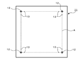
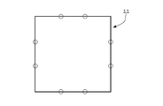
- FIG. 1 is a plan view of a mask blank glass substrate showing an example of arrangement of fiducial marks.
- two types of marks are formed: a rough alignment mark 12 having a relatively large size and a reference mark 13 of the present invention which is a small fine mark.
- these reference marks are shown on the surface of the glass substrate 11, but FIG. 1 merely shows an arrangement example of the reference marks on the main surface of the glass substrate. It is needless to say that the present invention is not limited to an embodiment in which the glass substrate is directly formed.
- the rough alignment mark 12 does not itself serve as a reference mark, but has a role for easily detecting the position of the reference mark 13.
- the fiducial mark 13 is small in size, and it is difficult to visually estimate the position. In addition, if it is attempted to detect the reference mark 13 from the beginning with inspection light or an electron beam, the detection takes a long time, and if a resist film is formed, unnecessary resist exposure may occur, which is not preferable.
- the reference mark 13 can be detected quickly and easily.
- FIG. 1 shows an example in which the rough alignment marks 12 are arranged at four locations near the corner on the main surface of the rectangular glass substrate 11 and the reference marks 13 are arranged at two locations near each rough alignment mark 12. ing.
- Both the rough alignment mark 12 and the reference mark 13 are preferably formed on the boundary line of the pattern formation region indicated by the broken line A on the main surface of the substrate, or on the outer peripheral side from the pattern formation region.
- too close to the outer periphery of the substrate is not preferable because the flatness of the main surface of the substrate may be a region where the flatness is not very good or may intersect with other types of recognition marks.
- the number of reference marks and rough alignment marks is not particularly limited. Although at least three reference marks are required, three or more reference marks may be used.
- the main mark is roughly specified around the main mark for determining a position (reference point) serving as a reference for the defect position. Since the auxiliary mark is arranged, the rough alignment mark 12 may not be provided if there is no particular inconvenience for detecting the reference mark 13 of the present invention from the beginning with inspection light or an electron beam. That is, in the present invention, as shown in FIG. 15, the rough alignment marks are not provided, and for example, the reference marks 13 of the present invention are arranged at four locations near the corner on the main surface of the glass substrate 11 as an example. It may be. As a result, the process of forming a relatively large rough alignment mark can be omitted, and the mark processing time can be greatly reduced.
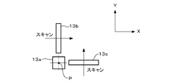
- FIG. 2 is a diagram showing a shape example and an arrangement example of the main mark and auxiliary mark constituting the reference mark of the present invention.
- FIG. 3 is a diagram for explaining a method of determining a reference point using the reference mark of the present invention.
- the reference mark serves as a reference for the defect position in the defect information.
- the reference mark 13 of the present invention includes a main mark for determining a position (reference point) to be a reference for the defect position, and the main mark.
- auxiliary marks arranged around the.
- the main mark has a point-symmetric shape and has a width of 200 nm or more and 10 ⁇ m or less with respect to the scanning direction of the electron beam or defect inspection light. Is to have.
- the main mark 13a has a polygonal shape having at least two sets of sides which are perpendicular to and parallel to the scanning direction of the electron beam drawing machine or the defect inspection light (X direction and Y direction in FIG. 3). Is preferred.
- the main mark 13a has a polygonal shape having at least two sets of sides that are perpendicular to and parallel to the scanning direction of the electron beam or the defect inspection light, so that it can be detected by the electron beam drawing machine and the defect inspection apparatus. And the variation of the defect detection position can be further suppressed.
- the main mark 13a is a square having the same length in both the vertical and horizontal directions (X and Y directions).
- the vertical and horizontal lengths (L) are 200 nm or more and 10 ⁇ m or less, respectively.
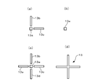
- the main mark 13a may be a point-symmetric shape. For example, as shown in FIG. 4A, the square corners are rounded, as shown in FIG. 4B, as shown in FIG. 4B, as shown in FIG. ) As shown in FIG. Also in this case, the size (length and width) L) of the main mark 13a is set to 200 nm or more and 10 ⁇ m or less. As a specific example, when the main mark 13a has a cross shape, the size (vertical and horizontal length) can be set to 5 ⁇ m or more and 10 ⁇ m or less. Although not shown, the main mark 13a may be a regular circle having a diameter of 200 nm to 10 ⁇ m.
- the two auxiliary marks 13b and 13c are arranged around the main mark 13a along the scanning direction of the electron beam or defect inspection light (X direction and Y direction in FIG. 3).
- the auxiliary marks 13b and 13c have a rectangular shape having a short side parallel to a long side perpendicular to the scanning direction of the electron beam or the defect inspection light. Since the auxiliary mark has a rectangular shape having a short side parallel to the long side perpendicular to the scanning direction of the electron beam or the defect inspection light, the auxiliary mark can be reliably detected by scanning with an electron beam drawing machine or a defect inspection device. The position of the main mark can be easily specified.
- the long side is a length that can be detected by the minimum number of scans of the electron beam drawing machine and the defect inspection apparatus. For example, it is desirable to have a length of 25 ⁇ m or more and 600 ⁇ m or less. On the other hand, if the length of the long side is short, for example, less than 25 ⁇ m, it may be difficult to detect the auxiliary mark by scanning with an electron beam drawing machine or a defect inspection apparatus. Further, if the length of the long side is long, for example, if it exceeds 600 ⁇ m, the processing time may exceed 1 hour / location depending on the method of forming the reference mark, which is not preferable. More preferably, the length of the long side is 25 ⁇ m or more and 400 ⁇ m or less, and more preferably 25 ⁇ m or more and 200 ⁇ m or less.
- auxiliary marks 13b and 13c and the main mark 13a may be separated from each other by a predetermined distance or may not be separated from each other.
- the interval is not particularly limited. However, in the present invention, it is preferable to set the distance to, for example, about 25 ⁇ m to 50 ⁇ m.
- Each of the main mark 13a and the auxiliary marks 13b and 13c has a concave cross-sectional shape and is a reference mark that can be recognized by providing a desired depth in the height direction of the reference mark.
- the cross-sectional shape is formed so as to spread from the bottom of the concave shape toward the surface side, and the inclination angle of the side wall of the reference mark in this case is It is preferably 75 ° or more. More preferably, it is 80 ° or more, and more preferably 85 ° or more.
- a reference point serving as a reference for the defect position is determined as follows (see FIG. 3).
- the position of the main mark 13a can be roughly specified by scanning the auxiliary marks 13b and 13c with an electron beam or defect inspection light in the X and Y directions and detecting these auxiliary marks. After scanning the electron beam or the inspection light in the X direction and the Y direction on the main mark 13a whose position is specified, the intersection P (usually the main mark) on the main mark 13a (detected by the scanning of the auxiliary mark) The reference point is determined with the approximate center of ().
- the main mark 13a has a point-symmetric shape and has a width of 200 nm or more and 10 ⁇ m or less with respect to the scanning direction of the electron beam or defect inspection light.
- the inventor examined the relationship between the width of the main mark 13a and the contrast with the electron beam, and the relationship between the width of the main mark 13a and the variation in the defect detection position.
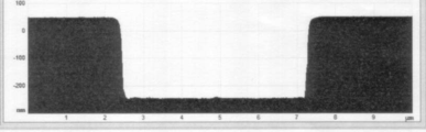
- FIG. 13 is a diagram showing the relationship between the width of the main mark and the electron beam contrast
- FIG. 14 is a diagram showing the relationship between the width of the main mark and the maximum variation in the defect detection position.
- FIG. 13 shows a multilayer reflective film (total film) in which a Si film (film thickness: 4.2 nm) and a Mo film (film thickness: 2.8 nm) are stacked for 40 periods on a SiO 2 —TiO 2 glass substrate.
- a square main mark is formed at a predetermined position (thickness: 280 nm) (all layers of the multilayer reflective film are removed by FIB).
- a Ru protective film film thickness: 2.5 nm
- an absorber film EB reflection intensity detected when EB (electron beam) is scanned on the main mark for a reflective mask blank with a resist film (total film thickness: 70 nm) and resist film (film thickness: 100 nm)
- FIG. 14 shows a multilayer reflective film in which a Si film (film thickness: 4.2 nm) and a Mo film (film thickness: 2.8 nm) are laminated on a SiO 2 —TiO 2 glass substrate for 40 periods.
- a defect inspection system (Teron600 series manufactured by KLA-Tencor) is applied to a substrate with a multilayer reflective film in which a square main mark is formed at a predetermined position (total thickness of 280 nm) (the multilayer reflective film is removed by FIB). This is the result of detecting the main mark and measuring the variation in the defect detection position.
- the variation in the defect detection position was determined by performing defect inspection five times and determining the variation in the defect position based on the detected reference coordinates.
- the width of the main mark 13a is less than 200 nm, the EB contrast is greatly reduced. That is, since it becomes difficult to detect the main mark by EB (electron beam) scanning, it is impossible to correct and correct the drawing data with high accuracy.
- the contrast when the width of the main mark 13a is 100 nm is 0.006, the contrast when the width is 200 nm is 0.016, and the difference in contrast is 2.75 times.
- the width of the main mark 13a exceeds 10 ⁇ m, the variation in the defect detection position exceeds 100 nm.
- the main mark 13a has a portion having a width of 200 nm to 10 ⁇ m with respect to the scanning direction of the electron beam or the defect inspection light. is there.
- the width is narrow (specifically, 30 to 100 nm as described in Patent Document 1), an absorber film or the like is formed thereon.
- the concave portion of the reference mark is filled, and there is a disadvantage that it is difficult to detect the reference mark.
- the auxiliary marks 13b and 13c preferably have a rectangular shape having a short side parallel to a long side perpendicular to the scanning direction of the electron beam or the defect inspection light. It is preferable that the side has a length that can be detected by the minimum number of scans of the electron beam drawing machine and the defect inspection apparatus, for example, a length of 25 ⁇ m to 600 ⁇ m. However, for example, if a length of about several hundred ⁇ m is formed with a focused ion beam, a long processing time is required. Therefore, the auxiliary mark can be divided into several rectangles as shown in FIG. FIG. 6 is an example specifically showing such an embodiment.
- One of the main marks 13a having a size of 5 ⁇ m ⁇ 5 ⁇ m (in the Y direction) has a rectangular auxiliary mark 13b1 having a size of 50 ⁇ m ⁇ 1 ⁇ m. 13b6 are arranged at equal intervals, and the interval (space) between the auxiliary marks is 50 ⁇ m.
- the auxiliary mark is removed in the first scan (first scan), the auxiliary mark is also removed in the second scan (second scan) shifted upward (Y direction) by 60 ⁇ m, and further shifted by 60 ⁇ m upward.
- the auxiliary mark 13b5 can be detected by the third scan (the third scan). Even if the auxiliary mark is divided in this way, and the long side length of each divided auxiliary mark is shortened, it is possible to determine the scanning rule and reliably detect the auxiliary mark with as few scans as possible. is there. Further, by dividing the auxiliary mark in this way, the overall processing time can be shortened.
- the position where the main mark 13a and the auxiliary marks 13b and 13c constituting the reference mark 13 of the present invention are formed is not particularly limited.
- it may be formed at any position as long as the multilayer reflective film is formed.
- any position of a substrate, a base layer (described later), a multilayer reflective film, a protective film (capping layer, buffer layer), an absorber film, and an etching mask film formed on the absorber film may be used.
- the reference mark after the formation of the reference mark, it is preferable to form the reference mark on the absorber film in the reflective mask blank from the viewpoint of suppressing a change in optical characteristics (for example, reflectance) due to cleaning.
- defect inspection in the reflective mask blank and defect coordinate management based on the reference mark can be performed as follows.
- a defect inspection apparatus performs defect inspection on the substrate with the multilayer reflection film formed on the substrate, using the center of the substrate main surface as a reference point, and the defect and position information detected by the defect inspection. And get.
- the reference mark of the present invention is formed at a predetermined position of the absorber film to obtain a reflective mask blank on which the reference mark is formed. Defect inspection is performed by a defect inspection apparatus with reference to the reference mark. Since the absorber film is formed on the multilayer reflective film as described above, the defect inspection data also reflects the defect inspection of the substrate with the multilayer reflective film obtained above.
- the defect inspection data of the substrate with the multilayer reflective film with the defect inspection data of the reflective mask blank can be obtained based on the reference mark.
- the method of forming the main mark 13a and the auxiliary marks 13b and 13c constituting the reference mark 13 of the present invention is not particularly limited.
- the cross-sectional shape of the above-mentioned reference mark is a concave shape
- the photolithographic method, the formation of a concave portion by laser light or ion beam, the processing mark by scanning a diamond needle, the indentation by a minute indenter, the stamping by the imprint method Can be formed.
- the reference mark of the present invention can be easily detected by either an electron beam drawing machine or an optical defect inspection apparatus, In other words, it can be reliably detected.
- the deviation of the reference point of the defect position determined by scanning with the electron beam or the defect inspection light can be reduced. Therefore, the variation in the defect detection position inspected based on the reference mark is small. Thereby, in the defect inspection, it is possible to determine the reference point of the defect position and acquire the accurate defect information (defect map) including the defect position (relative position of the reference point and the defect) information.
- the drawing data is corrected (corrected) with high accuracy so as to reduce the influence of the defect by collating with drawing data (mask pattern data) designed in advance based on the defect information.
- drawing data mask pattern data
- the present invention is not limited to such an embodiment.
- the position of the auxiliary mark relative to the main mark is arbitrary as long as the positional relationship between the main mark and the auxiliary mark is specified.
- the edge can be used as the reference point instead of the center of the main mark.
- the reference mark 13 of the present invention is formed on the boundary line of the pattern formation region indicated by the broken line A on the main surface of the substrate or at an arbitrary position on the outer peripheral side from the pattern formation region (FIG. 1, In this case, it is preferable to form a reference mark on the basis of an edge or specify a reference mark forming position with a coordinate measuring instrument after forming the reference mark.
- 17 and 18 are diagrams for explaining a method of forming a reference mark based on an edge.
- FIB focused ion beam
- the edge of the substrate with the multilayer reflective film is detected.
- the edge of the glass substrate 11 of the multilayer reflective film-coated substrate can be recognized by a secondary electron image, a secondary ion image, or an optical image.
- the reference mark is processed by other methods (for example, indentation), it can be recognized by an optical image. As shown in FIG.
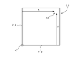
- the edge coordinates of eight sides (locations with circles) of the glass substrate 11 are confirmed, and tilt correction is performed.
- the origin in this case can be arbitrarily set, and may be the corner or center of the substrate.
- FIG. 18 shows a predetermined position from the origin O (0, 0) set at an arbitrary corner of the substrate on the basis of the edge, specifically, the X distance from the edge of the end face 11A on both sides of the origin O, and the end face 11B.
- the reference mark 13 is formed at a distance Y from the edge.
- the reference mark formation coordinates (X, Y) with reference to the origin O (0, 0) serve as reference mark formation position information. The same applies to the reference marks formed at other positions.
- the reference mark formation position can be easily specified.
- This coordinate measuring instrument measures the formation coordinates of a reference mark on the basis of an edge.
- a high-accuracy pattern position measuring device (LMS-IPRO4 manufactured by KLA-Tencor) can be used, and a specified reference mark is formed.
- the coordinates serve as reference mark formation position information.
- the coordinate measuring instrument also has a role of converting to the reference coordinates of the electron beam drawing machine, the user who is provided with the substrate with the multilayer reflective film can easily determine the defect position specified by the defect inspection apparatus based on the reference mark, It becomes possible to collate with drawing data with high accuracy, and defects in a finally manufactured mask can be reliably reduced.
- the reference mark 13 of the present invention is composed of the main mark and auxiliary mark described above, the width of the main mark is 200 nm to 10 ⁇ m, and the long side of the auxiliary mark is, for example, a size of 25 ⁇ m to 250 ⁇ m.
- the FIB as the reference mark forming means because the processing time of the reference mark can be shortened. Further, the detection time of the reference mark can be shortened, which is preferable.
- FIG. 16 shows an example of the shape and arrangement of the reference mark in the case of forming with the edge reference as described above.
- a configured reference mark is a typical example.
- the auxiliary mark is not necessarily required, and for example, only the main mark 13a as shown in FIG.
- a substrate with a multilayer reflective film in which the reference mark is formed at a predetermined position from the origin set with reference to the edge coordinates of the substrate and reference mark formation position information (reference mark formation coordinates) in this case
- reference mark formation position information reference mark formation coordinates
- the position of the reference mark is specified with a coordinate measuring instrument, and the substrate with the multilayer reflective film on which the reference mark is formed, and the formation of the reference mark in this case
- the user can reliably detect the reference mark in a short time using the reference mark formation position information.
- the reference coordinates of the electron beam drawing machine can be converted. Therefore, the user who is provided with the substrate with the multilayer reflective film can easily collate the defect position specified by the defect inspection apparatus based on the reference mark with the drawing data with high accuracy, and is finally manufactured. Defects can be reliably reduced in the mask.
- defect information position information, size, etc.
- the reference mark is added to the reference mark formation position information and provided to the user so that the user can use the reference mark formation position information.
- the reference mark can be reliably detected in a short time, and the drawing data is corrected (corrected) with high accuracy so as to reduce the influence of the defect based on the defect information. Defects can be reduced.
- a reflective mask blank in which an absorber film that absorbs EUV light is formed on the multilayer reflective film in the substrate with the multilayer reflective film on which the reference mark is formed is associated with the formation position information of the reference mark in association with the user.
- the user can reliably detect the reference mark in a short time using the reference mark formation position information in mask manufacturing using the reflective mask blank.
- the mask blank in which a thin film to be a transfer pattern is formed on the substrate the mask blank in which the reference mark is formed at a predetermined position from the origin set with reference to the edge coordinates of the substrate, and the reference in this case
- the mask blank in which the reference mark is formed by specifying the formation position of the reference mark with a coordinate measuring instrument after providing the user with the mark formation position information in association with each other or after forming the reference mark on the mask blank And the reference mark formation position information in this case are provided to the user in association with each other, so that the user can reliably detect the reference mark in a short time using the reference mark formation position information.
- the defect information based on the reference mark is added to the reference mark formation position information and provided to the user, so that the user can reduce the influence of the defect based on the defect information.
- the drawing data can be corrected (corrected) with high accuracy, and defects can be reduced in the finally manufactured mask.
- the present invention also provides a substrate 30 with a multilayer reflective film in which the reference mark 13 of the present invention is formed on the multilayer reflective film 31 that reflects EUV light.
- FIG. 7 shows an example in which the reference mark 13 is formed by removing a part of the film that forms the multilayer reflective film 31, but the reference mark 13 is formed by removing all the layers that constitute the multilayer reflective film 31. May be formed.
- the multilayer reflective film is a multilayer film in which a low refractive index layer and a high refractive index layer are alternately laminated. In general, a thin film of a heavy element or a compound thereof and a thin film of a light element or a compound thereof are alternately arranged. In addition, a multi-layer film laminated for about 40 to 60 periods is used.
- a Mo / Si periodic laminated film in which Mo films and Si films are alternately laminated for about 40 cycles is preferably used.
- Ru / Si periodic multilayer film, Mo / Be periodic multilayer film, Mo compound / Si compound periodic multilayer film, Si / Nb periodic multilayer film, Si / Mo / Examples include Ru periodic multilayer films, Si / Mo / Ru / Mo periodic multilayer films, and Si / Ru / Mo / Ru periodic multilayer films.
- the material may be appropriately selected depending on the exposure wavelength.
- the glass substrate 11 has a range of 0 ⁇ 1.0 ⁇ 10 ⁇ 7 / ° C., more preferably 0 ⁇ 0.3 ⁇ 10, in order to prevent distortion of the pattern due to heat during exposure.
- Those having a low thermal expansion coefficient in the range of ⁇ 7 / ° C. are preferably used, and as a material having a low thermal expansion coefficient in this range, for example, SiO 2 —TiO 2 glass, multicomponent glass ceramics, etc. are used. I can do it.
- the main surface of the glass substrate 11 on which the transfer pattern is formed is subjected to surface processing so as to have high flatness from the viewpoint of obtaining at least pattern transfer accuracy and position accuracy.
- the flatness is preferably 0.1 ⁇ m or less, particularly preferably 0.05 ⁇ m or less, in the main surface 142 mm ⁇ 142 mm region on the side where the transfer pattern of the glass substrate 11 is formed.
- the main surface opposite to the side on which the transfer pattern is formed is a surface that is electrostatically chucked when being set in the exposure apparatus, and has a flatness of 1 ⁇ m or less, preferably 0.8 mm in a 142 mm ⁇ 142 mm region. 5 ⁇ m or less.
- the glass substrate 11 of the multilayer reflective film-coated substrate as described above, a material having a low thermal expansion coefficient such as SiO 2 —TiO 2 glass is used.
- a material having a low thermal expansion coefficient such as SiO 2 —TiO 2 glass is used.
- As the surface roughness it is difficult to realize high smoothness of, for example, RMS of 0.1 nm or less. Therefore, as shown in FIG. 7, it is preferable to form a base layer 21 on the surface of the glass substrate 11 for the purpose of reducing the surface roughness of the glass substrate 11 or reducing defects on the surface of the glass substrate 11.
- the material for the underlayer 21 it is not necessary to have a light-transmitting property with respect to the exposure light, and a material that provides high smoothness and good defect quality when the surface of the underlayer is precisely polished is preferably selected. Is done.
- Si or a silicon compound containing Si for example, SiO 2 , SiON, etc.
- Si is particularly preferable.
- the surface of the underlayer 21 is preferably a surface that has been precisely polished so as to have the smoothness required for a mask blank substrate. It is desirable that the surface of the underlayer 21 be precisely polished so that the root mean square roughness (RMS) is 0.15 nm or less, particularly preferably 0.1 nm or less. Further, the surface of the underlayer 21 has Rmax / RMS of 2 to 10 in relation to the maximum surface roughness (Rmax) in consideration of the influence on the surface of the multilayer reflective film formed on the underlayer 21. In particular, it is desirable to perform precision polishing so as to be 2 to 8.
- the film thickness of the underlayer 21 is preferably in the range of 75 nm to 300 nm, for example.
- the present invention provides a reflective mask blank in which an absorber film serving as a transfer pattern is formed on the multilayer reflective film in the substrate with the multilayer reflective film having the above-described structure, and a thin film serving as a transfer pattern on a glass substrate for mask blank. Also provided is a mask blank in which is formed.
- the substrate with a multilayer reflective film is a reflective mask blank for manufacturing a reflective mask, that is, a multilayer reflective film that reflects exposure light (EUV light) on the substrate, and a pattern that absorbs exposure light (EUV light). It can be used as a substrate for a reflective mask blank provided with an absorber film for formation in order.
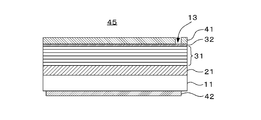
- FIG. 8 shows that a protective layer (capping layer) 32 and an absorber film 41 for pattern formation that absorbs EUV light are formed on the multilayer reflective film 31 in the substrate 30 with the multilayer reflective film on which the reference mark 13 of FIG. 7 is formed.
- the reflection type mask blank 40 currently formed is shown.
- a back conductive film 42 is provided on the side of the glass substrate 11 opposite to the side on which the multilayer reflective film or the like is formed.
- the absorber film 41 has a function of absorbing exposure light such as EUV light.
- tantalum (Ta) alone or a material containing Ta as a main component is preferably used.
- a material having Ta as a main component a material containing Ta and B, a material containing Ta and N, a material containing Ta and B and further containing at least one of O and N, a material containing Ta and Si, Ta A material containing Si and N, a material containing Ta and Ge, a material containing Ta, Ge and N are used.
- the protective film 32 and the buffer film are provided between the multilayer reflective film and the absorber film for the purpose of protecting the multilayer reflective film during patterning or pattern correction of the absorber film 41.
- the material for the protective film is mainly the above-described chromium-based material. Is used.
- the present invention also provides a reflective mask blank 45 in which the reference mark 13 of the present invention is formed on an absorber film 41 that absorbs EUV light, as shown in FIG. Note that, in FIG. 19, the same parts as those in FIG. FIG.
- the reference film 13 is formed by removing the absorber film 41 so that the protective film 32 is exposed.
- the reference mark 13 is formed by removing part of the absorber film 41.
- the reference mark 13 is formed so that the multilayer reflective film 31 is exposed by removing the absorber film 41 and the protective film 32, or the substrate film 11 is removed by removing the absorber film 41, the protective film 32, and the multilayer reflective film 31.
- the reference mark 13 may be formed so that is exposed.
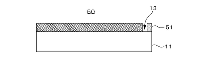
- FIG. 9 shows a binary mask blank 50 in which a light shielding film 51 is formed on the glass substrate 11.
- the reference mark 13 of the present invention is formed on the light shielding film 51.
- a phase shift mask blank can be obtained by providing a phase shift film or a phase shift film and a light shielding film on the glass substrate 11.
- the base layer 21 may be provided on the surface of the glass substrate 11 as necessary.
- This light shielding film may be a single layer or a plurality of layers (for example, a laminated structure of a light shielding layer and an antireflection layer).
- the light shielding layer may be composed of a plurality of layers.
- the phase shift film may be a single layer or a plurality of layers.
- a mask blank for example, a binary mask blank including a light shielding film formed of a material containing chromium (Cr), or a light shielding film formed of a material containing transition metal and silicon (Si).
- Binary mask blank provided, binary mask blank provided with light-shielding film formed of material containing tantalum (Ta), formed of material containing silicon (Si), or material containing transition metal and silicon (Si)
- a phase shift type mask blank provided with the phase shift film that is used.
- the material containing chromium (Cr) examples include chromium alone and chromium-based materials (CrO, CrN, CrC, CrON, CrCN, CrOC, CrOCN, etc.).
- chromium-based materials CrO, CrN, CrC, CrON, CrCN, CrOC, CrOCN, etc.
- tantalum (Ta) in addition to tantalum alone, a compound of tantalum and another metal element (for example, Hf, Zr, etc.), at least one of nitrogen, oxygen, carbon, and boron in addition to tantalum
- a material containing two elements specifically, a material containing TaN, TaO, TaC, TaB, TaON, TaCN, TaBN, TaCO, TaBO, TaBC, TaCON, TaBON, TaBCN, TaBCON, and the like.
- the material containing silicon (Si) a material further containing at least one element of nitrogen, oxygen, and carbon, specifically, a silicon nitride, an oxide, a carbide, an oxynitride, A material containing a carbonate or carbonitride is preferred.
- the material containing the transition metal and silicon (Si) in addition to the material containing the transition metal and silicon, the material further contains at least one element of nitrogen, oxygen and carbon in addition to the transition metal and silicon. Is mentioned. Specifically, a transition metal silicide or a material containing a transition metal silicide nitride, oxide, carbide, oxynitride, carbonate, or carbonitride is preferable.
- molybdenum As the transition metal, molybdenum, tantalum, tungsten, titanium, chromium, hafnium, nickel, vanadium, zirconium, ruthenium, rhodium, niobium, and the like are applicable. Of these, molybdenum is particularly preferred.
- the present invention also provides a reflective mask in which the absorber film in the reflective mask blank having the above configuration is patterned, and a mask in which the thin film in the mask blank having the above configuration is patterned.
- FIG. 10 shows a reflective mask 60 including an absorber film pattern 41a in which the absorber film 41 in the reflective mask blank 40 of FIG. 8 is patterned.
- FIG. 11 shows a binary mask 70 including a light shielding film pattern 51a in which the light shielding film 51 in the binary mask blank 50 of FIG. 9 is patterned.
- a method for patterning a thin film such as the absorber film or the light shielding film to be a transfer pattern in the mask blank a photolithography method is most preferable.
- a thin film to be a transfer pattern is patterned on the above-described mask blank glass substrate even in a phase shift mask blank having a structure including a phase shift film or a phase shift film and a light shielding film.
- a phase shift mask can be obtained.
- Example 1 A SiO 2 —TiO 2 glass substrate (size is about 152.) which is stepwise polished with cerium oxide abrasive grains or colloidal silica abrasive grains using a double-side polishing apparatus, and the substrate surface is surface-treated with low concentration silicic acid. 4 mm ⁇ about 152.4 mm and a thickness of about 6.35 mm). The surface roughness of the obtained glass substrate was 0.25 nm in terms of root mean square roughness (RMS) (measured with an atomic force microscope. The measurement area was 1 ⁇ m ⁇ 1 ⁇ m.).
- RMS root mean square roughness
- the flatness of the front and back surfaces of this glass substrate is about 290 nm. Met.
- the surface shape was adjusted by performing local surface processing on the glass substrate surface.
- the flatness of the front and back surfaces was 80 nm, which was 100 nm or less, in a 142 mm ⁇ 142 mm measurement region. there were.
- a B-doped Si target is used, a mixed gas of Ar gas and He gas is used as a sputtering gas, and a 100 nm Si underlayer is formed by DC magnetron sputtering, and then thermal energy is applied to the Si film.
- the stress reduction process was performed.
- the surface shape (surface morphology, flatness) and surface roughness of the obtained Si underlayer surface were measured, the measurement area of 142 mm ⁇ 142 mm was 80 nm and 100 nm or less. Moreover, the surface roughness was 0.08 nm in terms of root mean square roughness RMS in a measurement area of 1 ⁇ m ⁇ 1 ⁇ m, which was very good. Since RMS has an extremely high smoothness of 0.1 nm or less, background noise in a high-sensitivity defect inspection apparatus is reduced, and it is effective in terms of suppressing detection of pseudo defects. Further, the maximum surface roughness (Rmax) was 0.60 nm and Rmax / RMS was 7.5 in the measurement region of 1 ⁇ m ⁇ 1 ⁇ m, and the variation in surface roughness was small and good.
- a Si film (film thickness: 4.2 nm) and a Mo film (film thickness: 2.8 nm) are laminated on the Si underlayer for 40 periods, and multilayer reflection is performed.
- a film (total film thickness 280 nm) was formed to obtain a substrate with a multilayer reflective film.
- a reference mark having the following surface shape and a concave cross section was formed at a predetermined location on the surface of the multilayer reflective film.
- the reference mark was formed using a focused ion beam.
- the conditions at this time were an acceleration voltage of 50 kV and a beam current value of 20 pA.
- the above-mentioned main mark and auxiliary mark are formed as a reference mark so as to have an arrangement relationship as shown in FIG.
- the main mark 13a is a rectangle having a size of 5 ⁇ m ⁇ 5 ⁇ m, and the depth is set to about 280 nm because all layers constituting the multilayer reflective film are removed.
- the auxiliary marks 13b and 13c are both a rectangle having a size of 1 ⁇ m ⁇ 200 ⁇ m, and the depth is set to about 280 nm because all the layers constituting the multilayer reflective film are removed.
- the inclination angle of the side wall was 85 degrees, and the radius of curvature of the ridge line portion between the multilayer reflective film surface and the side wall was about
- the cross-sectional shape was as good as 250 nm.
- the fiducial mark formed on the multilayer reflective film has a high contrast of 0.025 and can be detected with high accuracy by an electron beam lithography apparatus or a blanks inspection apparatus, and the variation in the defect detection position is 83 nm or less and 100 nm or less. I confirmed that I can do it.
- the surface of the multilayer reflective film was inspected for defects using a blanks defect inspection apparatus (Teron 600 series manufactured by KLA-Tencor).
- a reference point is determined based on the above-described reference mark, and convex and concave defect position information and defect size information based on the relative position with the determined reference point are acquired, and a defect map is created.
- the reflectance of the multilayer reflective film surface of the substrate with the multilayer reflective film was evaluated by an EUV reflectometer, it was as good as 67% ⁇ 0.2% due to suppression of variations in the surface roughness of the underlayer. .
- a capping layer (film thickness: 2.5 nm) made of RuNb, a TaBN film (film thickness: 56 nm), and a TaBO film (film thickness: 14 nm) are laminated on the multilayer reflective film.
- An absorber layer made of a film was formed, and a CrN conductive film (film thickness: 20 nm) was formed on the back surface to obtain an EUV reflective mask blank.
- the obtained EUV reflective mask blank was subjected to defect inspection with a blanks defect inspection apparatus (Teron 600 series manufactured by KLA-Teccor). Similar to the above, the defect information obtained by obtaining the convex and concave defect position information and the defect size information using the above-mentioned reference mark as a reference, and making the EUV reflective mask blank correspond to these defect position information and defect size information. An attached EUV reflective mask blank was obtained.
- an EUV reflective mask was manufactured using this EUV reflective mask blank with defect information.
- an electron beam drawing resist was applied on an EUV reflective mask blank by a spin coating method and baked to form a resist film.
- mask pattern data designed in advance, and corrected to mask pattern data that does not affect pattern transfer using the exposure apparatus, or for pattern transfer. If it is determined that there is an effect, for example, if the defect is not corrected by mask pattern data with correction pattern data added so that the defect is hidden under the pattern, or if the corrected pattern data cannot be dealt with, the defect after mask fabrication The mask pattern data is corrected so that the load of correction can be reduced.
- a mask pattern is drawn and developed on the above-described resist film with an electron beam to form a resist pattern.
- the mask pattern data can be corrected with high accuracy.
- the absorber layer is removed by etching the TaBO film with a fluorine-based gas (CF 4 gas) and the TaBN film with a chlorine-based gas (Cl 2 gas) to form an absorber layer pattern on the capping layer. Formed. Further, the resist pattern remaining on the absorber layer pattern was removed with hot sulfuric acid to obtain an EUV reflective mask.
- the obtained EUV reflective mask was inspected with a mask defect inspection apparatus (Teron 600 series manufactured by KLA-Tencor), no convex defect was confirmed on the multilayer reflective film.
- Example 2 A reflective mask blank was produced in the same manner as in Example 1 except that the reference mark in Example 1 was not formed on the multilayer reflective film but was formed on the absorber film.
- the cross-sectional shape of the fiducial mark was observed with an atomic force microscope (AFM), as in Example 1, the inclination angle of the side wall was 87 degrees, and the radius of curvature of the ridgeline between the absorber film surface side wall was about 120 nm. And a good cross-sectional shape.
- the reference mark formed on the absorber film has a high contrast of 0.020 and can be detected with high accuracy by an electron beam lithography apparatus or a blanks defect inspection apparatus, and the variation of the defect detection position is 81 nm, so that the reproducibility is high. It was confirmed that it could be detected.
- the surface of the multilayer reflective film of the multilayer reflective film-coated substrate having the multilayer reflective film formed on the substrate is measured with a blanks defect inspection apparatus (Teron600 series manufactured by KLA-Tencor) as the center of the substrate main surface.
- a blanks defect inspection apparatus Teon600 series manufactured by KLA-Tencor
- the convex and concave defect position information and the defect size information are obtained with reference to the reference mark using the same blank defect inspection apparatus as described above.
- the defect information of the substrate with the multilayer reflective film and the defect information of the reflective mask blank by collating based on a plurality of defects that match, the reflective mask blank and these defect positions An EUV reflective mask blank with defect information corresponding to information and defect size information was obtained.
- Example 1 an EUV reflective mask was produced.
- the obtained EUV reflective mask was inspected with a mask defect inspection apparatus (Teron 600 series manufactured by KLA-Tencor), no convex defect was confirmed on the multilayer reflective film.
- a mask defect inspection apparatus Teon 600 series manufactured by KLA-Tencor
- the reflective mask thus obtained is set in an exposure apparatus and pattern transfer is performed on a semiconductor substrate on which a resist film is formed, there is no defect in the transfer pattern due to the reflective mask, and good pattern transfer can be performed. it can.
- Synthetic quartz substrate (size is about 152.4 mm x about 152.4 mm), which is polished stepwise with cerium oxide abrasive grains or colloidal silica abrasive grains using a double-side polishing machine, and the substrate surface is surface-treated with low concentration silicic acid. And a thickness of about 6.35 mm).
- the surface roughness of the obtained glass substrate was 0.2 nm in terms of root mean square roughness (RMS). Further, the flatness of the front and back surfaces of the glass substrate was about 290 nm.
- a light shielding film composed of a TaN film and a TaO film was formed on the glass substrate as follows.
- the TaN film was formed to a thickness of 44.9 nm by reactive sputtering (DC sputtering) at 1.5 kW, and subsequently, using a Ta target, a mixed gas atmosphere of argon (Ar) and oxygen (O 2 ) (
- a light-shielding film for ArF excimer laser (wavelength 193 nm) composed of the above laminate was formed to prepare a binary mask blank. The optical density of the light-shielding film with respect to ArF excimer laser was 3.0, and the surface reflectance was 19.5%.
- the same reference marks as in Example 1 were formed at predetermined locations on the surface of the light shielding film.
- the reference mark was formed using a focused ion beam.
- the conditions at this time were an acceleration voltage of 50 kV and a beam current value of 20 pA.
- the cross-sectional shape of the reference mark was observed with an atomic force microscope (AFM), as in Example 1, the inclination angle of the side wall was 83 degrees, and the curvature radius of the ridge line portion between the light shielding film surface and the side wall was about 300 nm.
- the cross-sectional shape was good.
- This reference mark formed on the light-shielding film has a high contrast of 0.02 and can be detected with high accuracy by an electron beam lithography apparatus or a blanks inspection apparatus, and it has been confirmed that the variation in defect detection position is 80 nm and can be detected with good reproducibility. .
- the obtained binary mask blank was subjected to defect inspection with a blanks defect inspection apparatus (Teron 600 series manufactured by KLA-Teccor). With reference to the reference mark formed on the above-mentioned light shielding film, the defect position information of the convex and concave and the defect size information are acquired, and the binary mask blank is associated with the defect position information and the defect size information. A binary mask blank was obtained.
- a binary mask was manufactured using this binary mask blank with defect information.
- an electron beam drawing resist was applied on a binary mask blank by a spin coating method and baked to form a resist film.
- the correction pattern data is corrected to the added mask pattern data, or for defects that cannot be dealt with even with the corrected pattern data, the load of defect correction after mask fabrication can be reduced.
- the mask pattern data was corrected, and based on the corrected mask pattern data, a mask pattern was drawn and developed on the above-described resist film with an electron beam to form a resist pattern. Also in the present embodiment, the relative positional relationship between the reference mark and the defect could be managed with high accuracy, so that the mask pattern data could be corrected with high accuracy.
- the TaO film was removed by etching with a fluorine-based gas (CF 4 gas) and the TaN film was etched with a chlorine-based gas (Cl 2 gas) to form a light-shielding film pattern. Further, the resist pattern remaining on the light shielding film pattern was removed with hot sulfuric acid to obtain a binary mask.
- a mask defect inspection apparatus Teon600 series manufactured by KLA-Tencor
- no convex defect was confirmed on the glass substrate.
- a reflective mask was prepared in order.
- a mask defect inspection apparatus Teon 600 series manufactured by KLA-Tencor
- several tens of convex defects were confirmed on the multilayer reflective film.
- the reason why several dozen convex defects were confirmed on the multilayer reflective film was examined in detail, and the detection reproducibility of the reference mark produced in this comparative example was poor (especially in the defect defect inspection apparatus). It was found that this was because correction / correction of the mask pattern data based on it could not be performed with high accuracy.
- Example 4 A reference mark having a concave cross section was formed at a predetermined location on the surface of the multilayer reflective film of the substrate with the multilayer reflective film of Example 1.
- the fiducial mark was formed using FIB (focused ion beam) as in Example 1.
- the conditions at this time were an acceleration voltage of 50 kV and a beam current value of 20 pA.
- the eight edge coordinates of the four sides of the substrate were confirmed, tilt correction was performed, and the origin was set at an arbitrary corner of the substrate. Then, a fiducial mark was formed by FIB at a predetermined position from the origin set by the edge reference in this way.
- reference marks are formed at positions of 8000 ⁇ m and 8000 ⁇ m from the respective edges of both end faces adjacent to the origin set at an arbitrary corner of the substrate on the basis of the edge, and in the same manner, a total of four locations within the substrate surface. Formed.
- the reference marks were formed such that the main marks and auxiliary marks described above were arranged as shown in FIG.
- the main mark 13a is a rectangle having a size of 5 ⁇ m ⁇ 5 ⁇ m, and the depth is set to about 280 nm because all layers constituting the multilayer reflective film are removed.
- auxiliary marks 13b and 13c are both a rectangle having a size of 1 ⁇ m ⁇ 120 ⁇ m, and the depth is set to about 280 nm because all layers constituting the multilayer reflective film are removed.
- This reference mark formed on the multilayer reflective film has the same high contrast as that of the first embodiment in the electron beam drawing apparatus or the blanks inspection apparatus, and uses the formation position information (reference mark formation coordinates) of the reference mark, It was confirmed that it can be detected accurately and in a short time. Compared with Example 1, the processing time of the reference mark could be shortened by about 30%.
- Example 5 A reference mark was formed on a substrate with a multilayer reflective film in the same manner as in Example 3 except that only a rectangular main mark having a size of 5 ⁇ m ⁇ 5 ⁇ m was used as the reference mark.
- This reference mark formed on the substrate with the multilayer reflective film is an electron beam lithography apparatus or a blanks inspection apparatus, and has a contrast as high as that of the first embodiment, and uses the formation position information (reference mark formation coordinates) of the reference mark. Thus, it was confirmed that it could be detected accurately and in a short time. Compared with Example 1, the processing time of the reference mark could be shortened by about 60%.
- Example 6 As a reference mark, only a rectangular main mark having a size of 5 ⁇ m ⁇ 5 ⁇ m was formed at an arbitrary position. Specifically, the reference mark was a reference mark having a concave cross-sectional shape at a predetermined position on the surface of the multilayer reflective film of the substrate with the multilayer reflective film of Example 1.
- the fiducial mark was formed using FIB (focused ion beam) as in Example 1. The conditions at this time were an acceleration voltage of 50 kV and a beam current value of 20 pA. Thereafter, the center coordinates of the reference mark were measured with a high-precision pattern position measuring device (LMS-IPRO4 manufactured by KLA-Tencor).
- LMS-IPRO4 high-precision pattern position measuring device
- This reference mark formed on the substrate with the multilayer reflective film is an electron beam lithography apparatus or a blanks inspection apparatus, and has a contrast as high as that of the first embodiment, and uses the formation position information (reference mark formation coordinates) of the reference mark. Thus, it was confirmed that it could be detected accurately and in a short time.
- the reference marks are formed by using the focused ion beam.
- the present invention is not limited to this. As described above, it can be formed by a photolithographic method, formation of a recess by a laser beam or the like, a processing mark obtained by scanning a diamond needle, an indentation by a minute indenter, a stamping by an imprint method, or the like.
- the example in which the base layer is formed on both the multilayer reflective film-coated substrate and the reflective mask blank has been described.
- the present invention is not limited to this. It may be a substrate with a multilayer reflective film in which an underlayer is not formed, or a reflective mask blank.
Abstract
Description
従来は、ブランクス検査等において、基板の欠陥の存在位置を、基板センターを原点(0,0)とし、その位置からの距離で特定していた。このため、位置精度が低く、装置間でも検出のばらつきがあり、パターン描画時に、欠陥を避けてパターン形成用薄膜にパターニングする場合でもμmオーダーでの回避は困難であった。このため、パターンを転写する方向を変えたり、転写する位置をmmオーダーでラフにずらして欠陥を回避していた。 As described above, as the demand for miniaturization in the lithography process increases, problems in the lithography process are becoming prominent. One of the problems is related to defect information on a mask blank substrate or the like used in a lithography process.
Conventionally, in a blank inspection or the like, the position of a substrate defect is specified by the distance from that position with the substrate center as the origin (0,0). For this reason, the positional accuracy is low, and there is a variation in detection between apparatuses, and it is difficult to avoid in the order of μm even when patterning is performed on a pattern forming thin film while avoiding defects. For this reason, the defect is avoided by changing the pattern transfer direction or by roughly shifting the transfer position on the order of mm.
特許文献1には、球相当直径で30nm程度の微小な欠陥の位置を正確に特定できるように、EUVリソグラフィ用反射型マスクブランク用基板の成膜面に、大きさが球相当直径で30~100nmの少なくとも3つのマークを形成することが開示されている。 Under such circumstances, for the purpose of increasing the inspection accuracy of the defect position, for example, a proposal has been made in which a reference mark is formed on a mask blank substrate and the position of the defect is specified using this as a reference position.
In Patent Document 1, a size equivalent to a sphere equivalent diameter of 30 to 30 mm is formed on the film forming surface of a reflective mask blank substrate for EUV lithography so that the position of a minute defect having a sphere equivalent diameter of about 30 nm can be accurately identified. It is disclosed to form at least three marks of 100 nm.
また最近では、マスクブランクの欠陥データとデバイスパターンデータとを元に、欠陥が存在している箇所に吸収体パターンが形成されるように描画データを補正して、欠陥を軽減させる試み(Defect mitigation technology)が提案されている。上述の技術を実現するためには、多層反射膜上に吸収体膜が形成され、さらに吸収体パターンを形成するためのレジスト膜が形成されたレジスト膜付きマスクブランクの状態で、電子線描画機においても電子線で基準マークを検出し、検出した基準点に基づいて、補正・修正した描画データを元に電子線描画が行われるが、基準マークについても、電子線走査に対して一定のコントラストが必要で、上記特許文献1に開示されている大きさのマークでは、電子線走査に対するコントラストが十分に得られないという問題がある。 It is theoretically possible to increase the inspection accuracy of the defect position of the mask blank by the method disclosed in Patent Document 1. However, since the mark size is as small as 30 to 100 nm in sphere equivalent diameter, for example, it is difficult to detect with a normally used defect inspection apparatus or the like, and there is a problem that the reproducibility of detection is poor. It is difficult to determine a reference position for identification. Patent Document 1 discloses that an auxiliary mark for identifying the mark is formed around the mark. The auxiliary mark is used to roughly specify the position where the mark is formed. Even if it can be done, the presence of the mark itself cannot be easily recognized unless a special inspection device with extremely high detection accuracy is used, so that it is difficult to specify an accurate reference point.
Recently, an attempt has been made to reduce defects by correcting drawing data so that an absorber pattern is formed at a position where a defect exists based on defect data and device pattern data of a mask blank (Defective mitigation). technology) has been proposed. In order to realize the above-described technique, an electron beam lithography machine is used in the state of a mask blank with a resist film in which an absorber film is formed on a multilayer reflective film and a resist film for forming an absorber pattern is further formed. The electron beam is detected based on the detected reference point and the electron beam is drawn based on the corrected / corrected drawing data. However, the reference mark also has a constant contrast with respect to the electron beam scanning. In the case of a mark having a size disclosed in Patent Document 1, there is a problem that sufficient contrast for electron beam scanning cannot be obtained.
すなわち、上記課題を解決するため、本発明は以下の構成を有する。
(構成1)
基板上にEUV光を反射する多層反射膜が形成されている多層反射膜付き基板であって、該多層反射膜付き基板に、欠陥情報における欠陥位置の基準となる基準マークが形成されており、前記基準マークは、前記欠陥位置の基準点を決定するためのメインマークを有し、前記メインマークは、点対称の形状であって、且つ、電子線又は欠陥検査光の走査方向に対して200nm以上10μm以下の幅の部分を有することを特徴とする多層反射膜付き基板。 The present inventor completed the present invention as a result of further intensive studies based on the above elucidated facts.
That is, in order to solve the above problems, the present invention has the following configuration.
(Configuration 1)
A substrate with a multilayer reflective film in which a multilayer reflective film that reflects EUV light is formed on the substrate, and a reference mark serving as a reference for a defect position in defect information is formed on the substrate with the multilayer reflective film, The reference mark has a main mark for determining a reference point of the defect position, and the main mark has a point-symmetric shape and 200 nm with respect to the scanning direction of the electron beam or the defect inspection light. A substrate with a multilayer reflective film, characterized by having a portion having a width of 10 μm or less.
基板上にEUV光を反射する多層反射膜が形成されている多層反射膜付き基板であって、該多層反射膜付き基板に、欠陥情報における欠陥位置の基準となる基準マークが形成されており、前記基準マークは、前記欠陥位置の基準点を決定するためのメインマークと、該メインマークの周囲に配置された補助マークとから構成され、前記メインマークは、点対称の形状であって、且つ、電子線又は欠陥検査光の走査方向に対して200nm以上10μm以下の幅の部分を有することを特徴とする多層反射膜付き基板。 (Configuration 2)
A substrate with a multilayer reflective film in which a multilayer reflective film that reflects EUV light is formed on the substrate, and a reference mark serving as a reference for a defect position in defect information is formed on the substrate with the multilayer reflective film, The reference mark is composed of a main mark for determining a reference point of the defect position, and an auxiliary mark arranged around the main mark, the main mark having a point-symmetric shape, and A substrate with a multilayer reflective film, having a portion having a width of 200 nm or more and 10 μm or less with respect to the scanning direction of the electron beam or defect inspection light.
前記メインマークは、電子線又は欠陥検査光の走査方向に対して垂直で且つ平行な辺を少なくとも2組有する多角形状であることを特徴とする構成1又は2に記載の多層反射膜付き基板。
構成3にあるように、前記メインマークは、電子線描画機又は欠陥検査光の走査方向に対して垂直で且つ平行な辺を少なくとも2組有する多角形状(例えば、四角形状、八角形状等)であることにより、電子線描画機、欠陥検査装置による検出の容易性(確実性)を向上させ、また、欠陥検出位置のばらつきを更に抑えることができる。 (Configuration 3)
3. The multilayer reflective film-coated substrate according to
As in Configuration 3, the main mark has a polygonal shape (for example, a quadrangular shape, an octagonal shape, etc.) having at least two sets of sides that are perpendicular to and parallel to the scanning direction of the electron beam drawing machine or the defect inspection light. As a result, the easiness (certainty) of detection by the electron beam drawing machine and the defect inspection apparatus can be improved, and the variation in the defect detection position can be further suppressed.
前記補助マークは、電子線又は欠陥検査光の走査方向に対して垂直な長辺と平行な短辺を有する矩形状であることを特徴とする構成1乃至3のいずれかに記載の多層反射膜付き基板。
構成4にあるように、前記補助マークは、電子線又は欠陥検査光の走査方向に対して垂直な長辺と平行な短辺を有する矩形状であることにより、電子線描画機、欠陥検査装置の走査により確実に検出できるため、メインマークの位置を容易に特定することができる。 (Configuration 4)
4. The multilayer reflective film according to claim 1, wherein the auxiliary mark has a rectangular shape having a short side parallel to a long side perpendicular to a scanning direction of an electron beam or defect inspection light. With board.
As in Configuration 4, the auxiliary mark has a rectangular shape having a short side parallel to a long side perpendicular to the scanning direction of the electron beam or the defect inspection light. Therefore, the position of the main mark can be easily specified.
前記基準マークは、前記多層反射膜に形成されていることを特徴とする構成1乃至4のいずれかに記載の多層反射膜付き基板。
構成5にあるように、前記基準マークを多層反射膜付き基板における多層反射膜に形成することにより、多層反射膜成膜後の欠陥検査において、電子線、及び欠陥検査光の走査で基準マークを検出し易くなる。また、描画データの補正・修正等によっても回避できない欠陥が発見された多層反射膜付き基板を廃棄せずに、多層反射膜を剥離除去してガラス基板を再生(再利用)することも可能である。 (Configuration 5)
The substrate with a multilayer reflective film according to any one of Structures 1 to 4, wherein the reference mark is formed on the multilayer reflective film.
As in
構成1乃至5のいずれかに記載の多層反射膜付き基板における前記多層反射膜上に、EUV光を吸収する吸収体膜が形成されていることを特徴とする反射型マスクブランク。
上記構成の多層反射膜付き基板における多層反射膜上に、転写パターンとなるEUV光を吸収する吸収体膜が形成されていることにより、欠陥情報における欠陥位置の基準となる基準マークが形成されている反射型マスクブランクが得られる。 (Configuration 6)
6. A reflective mask blank, wherein an absorber film that absorbs EUV light is formed on the multilayer reflective film in the multilayer reflective film-coated substrate according to any one of Structures 1 to 5.
On the multilayer reflective film in the substrate with the multilayer reflective film having the above structure, an absorber film that absorbs EUV light serving as a transfer pattern is formed, so that a reference mark serving as a reference for a defect position in defect information is formed. A reflective mask blank is obtained.
基板上にEUV光を反射する多層反射膜と、前記多層反射膜上に、EUV光を吸収する吸収体膜が形成されている反射型マスクブランクであって、該反射型マスクブランクに、欠陥情報における欠陥位置の基準となる基準マークが形成されており、前記基準マークは、前記欠陥位置の基準点を決定するためのメインマークを有し、前記メインマークは、点対称の形状であって、且つ、電子線又は欠陥検査光の走査方向に対して200nm以上10μm以下の幅の部分を有することを特徴とする反射型マスクブランク。
構成7にあるように、本発明に係る反射型マスクブランクは、欠陥情報における欠陥位置の基準となる基準マークが吸収体膜に形成されており、この基準マークは、前記欠陥位置の基準点を決定するためのメインマークを有している。そして、このメインマークは、点対称の形状であって、且つ、電子線又は欠陥検査光の走査方向に対して200nm以上10μm以下の幅の部分を有するものとなっている。このように構成された基準マークは、電子線描画機、光学式あるいはEUV光、電子線の欠陥検査装置のいずれでも容易に検出でき、言い換えれば確実に検出することができる。しかも、点対称の形状をしているので、電子線、欠陥検査光の走査によって決定される基準点のずれを小さくすることができる。また、エッジ基準で基準マークを形成したり、基準マークを任意の位置に形成後、座標計測器で基準マーク形成位置を特定することにより、基準マークのサイズをより小さくすることが可能であり、その場合、基準マークをメインマークのみとすることが可能である。このように基準マークのサイズを小さくできると、基準マークの形成手段として例えばFIB(集束イオンビーム)を使用した場合、加工時間が短縮でき、また基準マークの検出時間についても短縮できる。従って、基準マークを元に検査した欠陥検出位置のばらつきが小さい。また、これによって、欠陥検査においては、欠陥位置の基準点を決定し、欠陥位置(基準点と欠陥の相対位置)情報を含む精度の良い欠陥情報(欠陥マップ)を取得することができる。さらに、マスクの製造においては、この欠陥情報に基づいて、予め設計しておいた描画データ(マスクパターンデータ)と照合し、欠陥による影響が低減するように描画データを高い精度で修正(補正)することが可能になり、その結果として、最終的に製造される反射型マスクにおいて欠陥を低減させることができる。 (Configuration 7)
A reflective mask blank in which a multilayer reflective film that reflects EUV light on a substrate and an absorber film that absorbs EUV light is formed on the multilayer reflective film, and the defect information on the reflective mask blank A reference mark serving as a reference for the defect position is formed, the reference mark has a main mark for determining a reference point of the defect position, and the main mark has a point-symmetric shape, A reflective mask blank having a portion with a width of 200 nm or more and 10 μm or less with respect to the scanning direction of the electron beam or defect inspection light.
As in Configuration 7, in the reflective mask blank according to the present invention, a reference mark serving as a reference for the defect position in the defect information is formed on the absorber film, and the reference mark is a reference point for the defect position. It has a main mark for determination. The main mark has a point-symmetric shape and has a width of 200 nm to 10 μm with respect to the scanning direction of the electron beam or defect inspection light. The reference mark configured in this way can be easily detected by any of an electron beam drawing machine, an optical type or EUV light, and an electron beam defect inspection apparatus, in other words, can be reliably detected. In addition, since it has a point-symmetric shape, it is possible to reduce the deviation of the reference point determined by scanning with an electron beam and defect inspection light. In addition, it is possible to further reduce the size of the reference mark by forming a reference mark by edge reference, or by specifying the reference mark formation position with a coordinate measuring instrument after forming the reference mark at an arbitrary position. In that case, the reference mark can be the main mark only. If the size of the reference mark can be reduced in this way, when, for example, FIB (focused ion beam) is used as the reference mark forming means, the processing time can be shortened and the reference mark detection time can also be shortened. Therefore, the variation in the defect detection position inspected based on the reference mark is small. In addition, by this, in the defect inspection, it is possible to determine the reference point of the defect position and obtain accurate defect information (defect map) including the defect position (relative position between the reference point and the defect) information. Further, in the manufacture of the mask, the drawing data is corrected (corrected) with high accuracy so as to reduce the influence of the defect by collating with drawing data (mask pattern data) designed in advance based on the defect information. As a result, defects can be reduced in the finally manufactured reflective mask.
前記基準マークは、前記吸収体膜に形成されていることを特徴とする構成7記載の反射型マスクブランク。
構成8にあるように、前記吸収体膜に基準マークを形成する過程で、多層反射膜への欠陥発生のリスクが少ないこと、反射型マスクを作成する際には吸収体膜パターンとして加工する材料なので、FIBやエッチングで加工がしやすいこと、多層反射膜の膜厚に比べて吸収体膜の膜厚は薄いので、加工時間が短縮できること、等の利点を有するので好ましい。
(構成9)
前記基準マークは、前記メインマークと、該メインマークの周囲に配置された補助マークとから構成されていることを特徴とする構成7又は8記載の反射型マスクブランク。
構成9にあるように、基準マークは、メインマークと該メインマークの周囲に配置された補助マークとから構成されているので、電子描画機、光学式あるいはEUV光、電子線の欠陥検査装置でメインマークを検出しやすくなる。 (Configuration 8)
The reflective mask blank according to Configuration 7, wherein the reference mark is formed on the absorber film.
As in Structure 8, there is less risk of defect occurrence in the multilayer reflective film in the process of forming the reference mark on the absorber film, and a material that is processed as an absorber film pattern when creating a reflective mask Therefore, it is preferable because it has advantages such as easy processing by FIB and etching, and a thin film of the absorber film compared to the film thickness of the multilayer reflective film, so that the processing time can be shortened.
(Configuration 9)
9. The reflective mask blank according to Configuration 7 or 8, wherein the reference mark includes the main mark and auxiliary marks arranged around the main mark.
As described in Structure 9, since the reference mark is composed of a main mark and auxiliary marks arranged around the main mark, it can be used with an electronic drawing machine, an optical or EUV light, and an electron beam defect inspection apparatus. It becomes easier to detect the main mark.
前記メインマークは、電子線又は欠陥検査光の走査方向に対して垂直で且つ平行な辺を少なくとも2組有する多角形状であることを特徴とする構成7乃至9のいずれかに記載の反射型マスクブランク。
構成10にあるように、前記メインマークは、電子線描画機又は欠陥検査光の走査方向に対して垂直で且つ平行な辺を少なくとも2組有する多角形状(例えば、四角形状、八角形状等)であることにより、電子線描画機、欠陥検査装置による検出の容易性(確実性)を向上させ、また、欠陥検出位置のばらつきを更に抑えることができる。 (Configuration 10)
The reflective mask according to any one of Structures 7 to 9, wherein the main mark has a polygonal shape having at least two sets of sides that are perpendicular to and parallel to the scanning direction of the electron beam or the defect inspection light. blank.
As in
前記補助マークは、電子線又は欠陥検査光の走査方向に対して垂直な長辺と平行な短辺を有する矩形状であることを特徴とする構成9記載の反射型マスクブランク。
構成11にあるように、前記補助マークは、電子線又は欠陥検査光の走査方向に対して垂直な長辺と平行な短辺を有する矩形状であることにより、電子線描画機、欠陥検査装置の走査により確実に検出できるため、メインマークの位置を容易に特定することができる。
(構成12)
構成6乃至11のいずれかに記載の反射型マスクブランクにおける前記吸収体膜がパターニングされていることを特徴とする反射型マスク。
上記構成の反射型マスクブランクにおける吸収体膜がパターニングされて得られる反射型マスクは、多層反射膜付き基板又は反射型マスクブランクにおける欠陥情報に基づく描画データの補正・修正によって、欠陥を低減させたものが得られる。 (Configuration 11)
10. The reflective mask blank according to Configuration 9, wherein the auxiliary mark has a rectangular shape having a short side parallel to a long side perpendicular to the scanning direction of an electron beam or defect inspection light.
As in
(Configuration 12)
A reflective mask, wherein the absorber film in the reflective mask blank according to any one of Structures 6 to 11 is patterned.
The reflective mask obtained by patterning the absorber film in the reflective mask blank having the above configuration has reduced defects by correcting and correcting drawing data based on defect information in the substrate with the multilayer reflective film or the reflective mask blank. Things are obtained.
基板上に転写パターンとなる薄膜が形成されているマスクブランクであって、該マスクブランクに、欠陥情報における欠陥位置の基準となる基準マークが形成されており、前記基準マークは、前記欠陥位置の基準点を決定するためのメインマークを有し、前記メインマークは、点対称の形状であって、且つ、電子線又は欠陥検査光の走査方向に対して200nm以上10μm以下の幅の部分を有することを特徴とするマスクブランク。 (Configuration 13)
A mask blank in which a thin film to be a transfer pattern is formed on a substrate, and a reference mark serving as a reference of a defect position in defect information is formed on the mask blank, and the reference mark A main mark for determining a reference point, the main mark having a point-symmetric shape and having a width of 200 nm to 10 μm with respect to the scanning direction of the electron beam or defect inspection light; A mask blank characterized by that.
基板上に転写パターンとなる薄膜が形成されているマスクブランクであって、該マスクブランクに、欠陥情報における欠陥位置の基準となる基準マークが形成されており、前記基準マークは、前記欠陥位置の基準点を決定するためのメインマークと、該メインマークの周囲に配置された補助マークとから構成され、前記メインマークは、点対称の形状であって、且つ、電子線又は欠陥検査光の走査方向に対して200nm以上10μm以下の幅の部分を有することを特徴とするマスクブランク。 (Configuration 14)
A mask blank in which a thin film to be a transfer pattern is formed on a substrate, and a reference mark serving as a reference of a defect position in defect information is formed on the mask blank, and the reference mark It is composed of a main mark for determining a reference point and auxiliary marks arranged around the main mark. The main mark has a point-symmetric shape and is scanned with an electron beam or defect inspection light. A mask blank having a width of 200 nm to 10 μm with respect to the direction.
構成13又は14に記載のマスクブランクにおける前記薄膜がパターニングされていることを特徴とするマスク。
上記構成のマスクブランクにおける薄膜がパターニングされて得られるマスクは、マスクブランクにおける欠陥情報に基づく描画データの修正によって、欠陥を低減させたものが得られる。 (Configuration 15)
The mask, wherein the thin film in the mask blank according to
A mask obtained by patterning a thin film in the mask blank having the above-described configuration can be obtained by reducing defects by correcting drawing data based on defect information in the mask blank.
構成1乃至5のいずれかに記載の多層反射膜付き基板の製造方法であって、前記基準マークを、前記基板のエッジ座標を基準に設定した原点からの所定の位置に形成し、前記基準マークを形成した前記多層反射膜付き基板と、前記基準マークの形成位置情報とを対応付けることを特徴とする多層反射膜付き基板の製造方法。
このように、基板のエッジ座標を基準に設定した原点からの所定の位置に前記基準マークを形成した多層反射膜付き基板と、前記基準マークの形成位置情報とを対応付けて多層反射膜付き基板を製造することにより、この多層反射膜付き基板を提供されたユーザーは、この基準マークの形成位置情報を利用して基準マークを短時間で確実に検出することができる。 (Configuration 16)
6. The method for manufacturing a substrate with a multilayer reflective film according to any one of Structures 1 to 5, wherein the reference mark is formed at a predetermined position from an origin set with reference to an edge coordinate of the substrate, and the reference mark A method for manufacturing a substrate with a multilayer reflective film, comprising associating the substrate with a multilayer reflective film formed with the reference mark formation position information.
As described above, the multilayer reflective film-coated substrate in which the reference mark is formed at a predetermined position from the origin set based on the edge coordinates of the substrate and the formation position information of the reference mark are associated with each other. By manufacturing this, the user who is provided with the multilayer reflective film-coated substrate can reliably detect the reference mark in a short time using the reference mark formation position information.
構成1乃至5のいずれかに記載の多層反射膜付き基板の製造方法であって、前記基準マークを形成した後、座標計測器で前記基準マークの形成位置を特定し、前記基準マークを形成した前記多層反射膜付き基板と、前記基準マークの形成位置情報とを対応付けることを特徴とする多層反射膜付き基板の製造方法。
このように、多層反射膜付き基板に基準マークを形成した後、座標計測器で前記基準マークの形成位置を特定し、前記基準マークを形成した多層反射膜付き基板と、前記基準マークの形成位置情報とを対応付けて多層反射膜付き基板を製造することにより、この多層反射膜付き基板を提供されたユーザーは、この基準マークの形成位置情報を利用して基準マークを短時間で確実に検出することができる。また、基準マークの形成位置を座標計測器で特定することにより、電子線描画機の基準座標の変換が可能となる。したがって、多層反射膜付き基板を提供されたユーザーは、容易に基準マークに基づき欠陥検査装置により特定した欠陥位置と、描画データとを高精度に照合することが可能となり、最終的に製造されるマスクにおいて欠陥を確実に低減させることができる。 (Configuration 17)
A method for manufacturing a substrate with a multilayer reflective film according to any one of Structures 1 to 5, wherein after forming the reference mark, a position of the reference mark is specified by a coordinate measuring instrument, and the reference mark is formed. A method for producing a substrate with a multilayer reflective film, wherein the substrate with a multilayer reflective film and the formation position information of the reference mark are associated with each other.
Thus, after forming the reference mark on the substrate with the multilayer reflective film, the position of the reference mark is specified by a coordinate measuring instrument, the substrate with the multilayer reflective film on which the reference mark is formed, and the position of the reference mark By manufacturing a substrate with a multilayer reflective film in association with information, a user who is provided with this multilayer reflective film substrate can reliably detect the reference mark in a short time using the information on the formation position of this reference mark. can do. In addition, by specifying the formation position of the reference mark with the coordinate measuring instrument, the reference coordinates of the electron beam drawing machine can be converted. Therefore, the user who is provided with the substrate with the multilayer reflective film can easily collate the defect position specified by the defect inspection apparatus based on the reference mark with the drawing data with high accuracy, and is finally manufactured. Defects can be reliably reduced in the mask.
前記基準マークの形成位置情報に、さらに前記基準マークを基準とした欠陥情報を加えることを特徴とする構成16又は17に記載の多層反射膜付き基板の製造方法。
構成18にあるように、前記基準マークの形成位置情報に、さらに前記基準マークを基準とした欠陥情報を加えて多層反射膜付き基板を製造することにより、この多層反射膜付き基板を提供されたユーザーはこの基準マークの形成位置情報を利用して基準マークを短時間で確実に検出することができるとともに、マスクの製造においては、この欠陥情報に基づいて、欠陥による影響が低減するように描画データを高い精度で修正(補正)し、最終的に製造されるマスクにおいて欠陥を低減させることができる。 (Configuration 18)
18. The method for manufacturing a substrate with a multilayer reflective film according to Configuration 16 or 17, wherein defect information based on the reference mark is further added to the formation position information of the reference mark.
According to the configuration 18, the substrate with the multilayer reflective film is provided by adding the defect information based on the reference mark to the formation position information of the reference mark and manufacturing the substrate with the multilayer reflective film. The user can detect the fiducial mark reliably in a short time using the fiducial mark formation position information, and in the mask manufacturing, the drawing is performed so that the influence of the defect is reduced based on the defect information. The data can be corrected (corrected) with high accuracy, and defects can be reduced in the finally manufactured mask.
構成16乃至18のいずれかに記載の前記基準マークを形成した前記多層反射膜付き基板における前記多層反射膜上に、EUV光を吸収する吸収体膜が形成されている反射型マスクブランクと、前記基準マークの形成位置情報とを対応付けることを特徴とする反射型マスクブランクの製造方法。
構成19のように、構成16乃至18のいずれかに記載の前記基準マークを形成した多層反射膜付き基板における多層反射膜上に、EUV光を吸収する吸収体膜が形成された反射型マスクブランクと、前記基準マークの形成位置情報とを対応付けてユーザーに提供することにより、ユーザーは、この反射型マスクブランクを用いるマスク製造において、この基準マークの形成位置情報を利用して基準マークを短時間で確実に検出することができる。 (Configuration 19)
A reflective mask blank in which an absorber film that absorbs EUV light is formed on the multilayer reflective film in the multilayer reflective film-coated substrate on which the reference mark according to any one of configurations 16 to 18 is formed; A method of manufacturing a reflective mask blank, characterized by associating with reference mark formation position information.
A reflective mask blank in which an absorber film that absorbs EUV light is formed on a multilayer reflective film in a substrate with a multilayer reflective film in which the reference mark according to any one of Structures 16 to 18 is formed as in Configuration 19. And the reference mark formation position information in association with each other, the user can shorten the reference mark using the reference mark formation position information in mask manufacturing using the reflective mask blank. It can be reliably detected in time.
構成6乃至11のいずれかに記載の反射型マスクブランクの製造方法であって、前記基準マークを、前記基板のエッジ座標を基準に設定した原点からの所定の位置に形成し、前記基準マークを形成した前記反射型マスクブランクと、前記基準マークの形成位置情報とを対応付けることを特徴とする反射型マスクブランクの製造方法。
このように、基板のエッジ座標を基準に設定した原点からの所定の位置に前記基準マークを形成した反射型マスクブランクと、前記基準マークの形成位置座標とを対応付けて反射型マスクブランクを製造することにより、この反射型マスクブランクを提供されたユーザーは、この基準マークの形成位置情報を利用して基準マークを短時間で確実に検出することができる。 (Configuration 20)
The method of manufacturing a reflective mask blank according to any one of Structures 6 to 11, wherein the reference mark is formed at a predetermined position from an origin set with reference to an edge coordinate of the substrate, and the reference mark is formed. A method of manufacturing a reflective mask blank, wherein the formed reflective mask blank is associated with formation position information of the reference mark.
Thus, a reflective mask blank is manufactured by associating the reflective mask blank in which the reference mark is formed at a predetermined position from the origin set with reference to the edge coordinates of the substrate, and the formation position coordinate of the reference mark. Thus, the user who is provided with the reflective mask blank can reliably detect the reference mark in a short time by using the formation position information of the reference mark.
請求項6乃至11のいずれかに記載の反射型マスクブランクの製造方法であって、前記基準マークを形成した後、座標計測器で前記基準マークの形成位置を特定し、前記基準マークを形成した前記反射型マスクブランクと、前記基準マークの形成位置情報とを対応付けることを特徴とする反射型マスクブランクの製造方法。
このように、反射型マスクブランクに基準マークを形成した後、座標計測器で前記基準マークの形成位置を特定し、前記基準マークを形成した反射型マスクブランクと、前記基準マークの形成位置情報とを対応付けて反射型マスクブランクを製造することにより、この反射型マスクブランクを提供されたユーザーは、この基準マークの形成位置情報を利用して基準マークを短時間で確実に検出することができる。また、基準マークの形成位置を座標計測器で特定することにより、電子線描画機の基準座標の変換が可能となる。したがって、多層反射膜付き基板を提供されたユーザーは、容易に基準マークに基づき欠陥検査装置により特定した欠陥位置と、描画データとを高精度に照合することが可能となり、最終的に製造されるマスクにおいて欠陥を確実に低減させることができる。 (Configuration 21)
It is a manufacturing method of the reflective mask blank in any one of Claims 6 thru | or 11, Comprising: After forming the said reference mark, the formation position of the said reference mark was specified with the coordinate measuring device, and the said reference mark was formed. A method of manufacturing a reflective mask blank, wherein the reflective mask blank and the reference mark formation position information are associated with each other.
Thus, after forming the reference mark on the reflective mask blank, the coordinate mark is used to identify the formation position of the reference mark, the reflective mask blank on which the reference mark is formed, and the formation position information of the reference mark. By manufacturing the reflective mask blank in association with each other, the user who is provided with this reflective mask blank can reliably detect the reference mark in a short time using the formation position information of the reference mark. . In addition, by specifying the formation position of the reference mark with the coordinate measuring instrument, the reference coordinates of the electron beam drawing machine can be converted. Therefore, the user who is provided with the substrate with the multilayer reflective film can easily collate the defect position specified by the defect inspection apparatus based on the reference mark with the drawing data with high accuracy, and is finally manufactured. Defects can be reliably reduced in the mask.
構成13又は14に記載のマスクブランクの製造方法であって、前記基準マークを、前記基板のエッジ座標を基準に設定した原点からの所定の位置に形成し、前記基準マークを形成した前記マスクブランクと、前記基準マークの形成位置情報とを対応付けることを特徴とするマスクブランクの製造方法。
構成22にあるように、基板のエッジ座標を基準に設定した原点からの所定の位置に前記基準マークを形成したマスクブランクと、前記基準マークの形成位置情報とを対応付けてマスクブランクを製造することにより、このマスクブランクを提供されたユーザーは、この基準マークの形成位置情報を利用して基準マークを短時間で確実に検出することができる。 (Configuration 22)
The mask blank manufacturing method according to
As in Configuration 22, a mask blank is manufactured by associating a mask blank in which the reference mark is formed at a predetermined position from the origin set with reference to the edge coordinates of the substrate and the formation position information of the reference mark. Thus, the user who is provided with the mask blank can reliably detect the reference mark in a short time by using the formation position information of the reference mark.
構成13又は14に記載のマスクブランクの製造方法であって、前記基準マークを形成した後、座標計測器で前記基準マークの形成位置を特定し、前記基準マークを形成した前記マスクブランクと、前記基準マークの形成位置情報とを対応付けることを特徴とするマスクブランクの製造方法。
構成23のように、マスクブランクに基準マークを形成した後、座標計測器で前記基準マークの形成位置を特定し、前記基準マークを形成したマスクブランクと、前記基準マークの形成位置情報とを対応付けてマスクブランクを製造することによりマスクブランクを提供されたユーザーは、この基準マークの形成位置情報を利用して基準マークを短時間で確実に検出することができる。また、基準マークの形成位置を座標計測器で特定することにより、電子線描画機の基準座標の変換が可能となる。したがって、マスクブランクを提供されたユーザーは、容易に基準マークに基づき欠陥検査装置により特定した欠陥位置と、描画データとを高精度に照合することが可能となり、最終的に製造されるマスクにおいて欠陥を確実に低減させることができる。 (Configuration 23)
The mask blank manufacturing method according to
After forming the reference mark on the mask blank as in Configuration 23, the coordinate mark is used to identify the formation position of the reference mark, and the mask blank on which the reference mark is formed corresponds to the formation position information of the reference mark. In addition, a user who is provided with a mask blank by manufacturing the mask blank can reliably detect the reference mark in a short time using the formation position information of the reference mark. In addition, by specifying the formation position of the reference mark with the coordinate measuring instrument, the reference coordinates of the electron beam drawing machine can be converted. Therefore, the user who is provided with the mask blank can easily collate the defect position specified by the defect inspection apparatus based on the reference mark with the drawing data with high accuracy, and the defect in the finally manufactured mask Can be reliably reduced.
前記基準マークの形成位置情報に、さらに前記基準マークを基準とした欠陥情報を加えることを特徴とする構成22又は23に記載のマスクブランクの製造方法。
構成24にあるように、前記基準マークの形成位置情報に、さらに前記基準マークを基準とした欠陥情報を加えてユーザーに提供することにより、ユーザーはこの基準マークの形成位置情報を利用して基準マークを短時間で確実に検出することができるとともに、マスクの製造においては、この欠陥情報に基づいて、欠陥による影響が低減するように描画データを高い精度で修正(補正)し、最終的に製造されるマスクにおいて欠陥を低減させることができる。 (Configuration 24)
24. The method of manufacturing a mask blank according to Configuration 22 or 23, wherein defect information based on the reference mark is further added to the formation position information of the reference mark.
According to the structure 24, the defect information based on the reference mark is further added to the reference mark formation position information and provided to the user, so that the user can use the reference mark formation position information as a reference. Marks can be detected reliably in a short time, and in mask manufacturing, drawing data is corrected (corrected) with high accuracy so that the influence of defects is reduced based on this defect information. Defects can be reduced in the manufactured mask.
また、本発明によれば、これら多層反射膜付き基板、マスクブランクを使用し、これらの欠陥情報に基づき、描画データの修正を行なうことで欠陥を低減させた反射型マスク及びマスクを提供することができる。
また、本発明によれば、エッジ基準で基準マークを形成したり、或いは基準マークの形成後、座標計測器で基準マーク形成位置を特定した多層反射膜付き基板、反射型マスクブランク及びマスクブランクと、これらの基準マークの形成位置情報とを対応付けした多層反射膜付き基板、反射型マスクブランク及びマスクブランクの製造方法を提供することができる。 According to the present invention, a reference mark that can be reliably detected by either an electron beam drawing machine or a defect inspection apparatus, and that has a small deviation of the reference point of the defect position determined by scanning of the electron beam and the defect inspection light. By forming the substrate, it is possible to provide a substrate with a multilayer reflective film, a reflective mask blank, and a mask blank capable of highly accurately performing defect coordinate management (reference mark and defect relative position management).
In addition, according to the present invention, there is provided a reflective mask and a mask in which defects are reduced by using these multilayer reflective film-coated substrates and mask blanks and correcting drawing data based on these defect information. Can do.
In addition, according to the present invention, a reference mark is formed based on an edge reference, or after forming the reference mark, a substrate with a multilayer reflective film, a reflective mask blank, and a mask blank whose reference mark formation position is specified by a coordinate measuring instrument, In addition, it is possible to provide a substrate with a multilayer reflective film, a reflective mask blank, and a method for manufacturing the mask blank, which are associated with the formation position information of these reference marks.
[基準マーク]
まず、本発明における基準マーク(以下、「本発明の基準マーク」とも呼ぶ。)について詳しく説明する。
図1は、基準マークの配置例を示すマスクブランク用ガラス基板の平面図である。
図1では、相対的に大きさの大きなラフアライメントマーク12と小さなファインマークである本発明の基準マーク13の2種類のマークを形成している。なお、図1では、ガラス基板11の表面にこれら基準マークを示しているが、図1はあくまでもガラス基板主表面上での基準マークの配置例を示すものであり、本発明をこれら基準マークがガラス基板に直接形成されている態様に限定する趣旨ではないことは勿論である。 Hereinafter, embodiments of the present invention will be described in detail.
[Reference mark]
First, the reference mark in the present invention (hereinafter also referred to as “reference mark of the present invention”) will be described in detail.
FIG. 1 is a plan view of a mask blank glass substrate showing an example of arrangement of fiducial marks.
In FIG. 1, two types of marks are formed: a
基準マーク、ラフアライメントマークの個数は特に限定されない。基準マークについては、最低3個必要であるが、3個以上であっても構わない。 FIG. 1 shows an example in which the rough alignment marks 12 are arranged at four locations near the corner on the main surface of the
The number of reference marks and rough alignment marks is not particularly limited. Although at least three reference marks are required, three or more reference marks may be used.
すなわち、本発明においては、図15に示すように、上記ラフアライメントマークは設けずに、例えば一例としてガラス基板11の主表面上のコーナー近傍の4箇所に本発明の基準マーク13を配置するようにしてもよい。これによって、相対的に大きさの大きなラフアライメントマークの形成工程を省くことができ、マークの加工時間を大幅に短縮できる。 As will be described below, in the
That is, in the present invention, as shown in FIG. 15, the rough alignment marks are not provided, and for example, the reference marks 13 of the present invention are arranged at four locations near the corner on the main surface of the
上記基準マークは、欠陥情報における欠陥位置の基準となるものであるが、本発明の基準マーク13は、欠陥位置の基準となる位置(基準点)を決定するためのメインマークと、該メインマークの周囲に配置された補助マークとから構成される。そして、本発明の基準マークにおける特徴の一つは、上記メインマークは、点対称の形状であって、且つ、電子線又は欠陥検査光の走査方向に対して200nm以上10μm以下の幅の部分を有することである。 FIG. 2 is a diagram showing a shape example and an arrangement example of the main mark and auxiliary mark constituting the reference mark of the present invention. FIG. 3 is a diagram for explaining a method of determining a reference point using the reference mark of the present invention.
The reference mark serves as a reference for the defect position in the defect information. However, the
本発明において、上記メインマーク13aは、電子線描画機又は欠陥検査光の走査方向(図3におけるX方向及びY方向)に対して垂直で且つ平行な辺を少なくとも2組有する多角形状であることが好適である。このように、上記メインマーク13aは、電子線又は欠陥検査光の走査方向に対して垂直で且つ平行な辺を少なくとも2組有する多角形状であることにより、電子線描画機、欠陥検査装置による検出の容易性(確実性)を向上させ、また、欠陥検出位置のばらつきを更に抑えることができる。図2及び図3では、具体例として、上記メインマーク13aが、縦横(X及びY方向)が同じ長さの正方形である場合を示している。この場合、縦横の長さ(L)がそれぞれ200nm以上10μm以下である。 2 and 3 show, as an example, a
In the present invention, the
なお、上記メインマーク13a、補助マーク13b、13cはいずれも断面形状を凹形状とし、基準マークの高さ方向に所望の深さを設けることで認識し得る基準マークとしている。電子線や欠陥検査光による検出精度を向上させる観点から、凹形状の底部から表面側へ向かって広がるように形成された断面形状であることが好ましく、この場合の基準マークの側壁の傾斜角度は75°以上であることが好ましい。さらに好ましくは、80°以上、さらに好ましくは、85°以上とすることが望ましい。 Further, the
Each of the
上記補助マーク13b,13c上を電子線、あるいは欠陥検査光がX方向、Y方向に走査し、これら補助マークを検出することにより、メインマーク13aの位置を大まかに特定することができる。位置が特定された上記メインマーク13a上を電子線、あるいは検査光がX方向及びY方向に走査後、(上記補助マークの走査により検出された)メインマーク13a上の交点P(通常、メインマークの略中心)をもって基準点を決定する。 Using the reference mark, a reference point serving as a reference for the defect position is determined as follows (see FIG. 3).
The position of the
また、たとえば基準マークを多層反射膜に形成した場合、その幅が狭いと(具体的には、特許文献1に記載されているような30~100nmであると)、その上に吸収体膜等を成膜すると、基準マークの凹部が埋まってしまい、基準マークを検出することが困難になるという不都合も生じる。 As shown in FIG. 13, when the width of the
For example, when the reference mark is formed on the multilayer reflective film, if the width is narrow (specifically, 30 to 100 nm as described in Patent Document 1), an absorber film or the like is formed thereon. When the film is formed, the concave portion of the reference mark is filled, and there is a disadvantage that it is difficult to detect the reference mark.
そこで、上記補助マークを、図5に示すように、いくつかの矩形に分割することができる。図6は、このような態様を具体的に示した例であり、5μm×5μmの大きさのメインマーク13aの一方(Y方向)に、50μm×1μmの大きさの矩形状の補助マーク13b1~13b6を等間隔で配置し、各補助マーク間の間隔(スペース)は50μmとする。 By the way, as described above, the
Therefore, the auxiliary mark can be divided into several rectangles as shown in FIG. FIG. 6 is an example specifically showing such an embodiment. One of the
このように補助マークを分割し、分割した個々の補助マークの長辺の長さを短くしても、走査ルールを決めて、出来るだけ少ない走査回数で補助マークを確実に検出することが可能である。また、このように補助マークを分割することで、全体の加工時間の短縮が図れる。 In this case, for example, the auxiliary mark is removed in the first scan (first scan), the auxiliary mark is also removed in the second scan (second scan) shifted upward (Y direction) by 60 μm, and further shifted by 60 μm upward. Further, the auxiliary mark 13b5 can be detected by the third scan (the third scan).
Even if the auxiliary mark is divided in this way, and the long side length of each divided auxiliary mark is shortened, it is possible to determine the scanning rule and reliably detect the auxiliary mark with as few scans as possible. is there. Further, by dividing the auxiliary mark in this way, the overall processing time can be shortened.
また、基準マーク形成後、洗浄による光学特性(たとえば、反射率)の変化を抑制する観点からは、反射型マスクブランクにおける吸収体膜に基準マークを形成することが好ましい。この場合、多層反射膜付き基板の段階では基準マークが形成されていないので、反射型マスクブランクにおける欠陥検査と、基準マークを基準にした欠陥の座標管理は以下のようにして行うことができる。 Note that in a reflective mask that uses EUV light as exposure light, defects present in the multilayer reflective film are almost impossible to correct and can become serious phase defects on the transfer pattern. In order to reduce defects, defect information on the multilayer reflective film is important. Therefore, it is desirable to obtain defect information by performing defect inspection at least after the multilayer reflective film is formed. For that purpose, it is preferable to form the fiducial mark of the present invention on a substrate with a multilayer reflective film. In particular, it is preferable to form the fiducial mark of the present invention on the multilayer reflective film from the viewpoint of easy detection and substrate regeneration.
In addition, after the formation of the reference mark, it is preferable to form the reference mark on the absorber film in the reflective mask blank from the viewpoint of suppressing a change in optical characteristics (for example, reflectance) due to cleaning. In this case, since the reference mark is not formed at the stage of the substrate with the multilayer reflective film, defect inspection in the reflective mask blank and defect coordinate management based on the reference mark can be performed as follows.
上記の基準マークを基準にして欠陥検査装置により欠陥検査を行う。上記の通り吸収体膜は多層反射膜上に形成するので、この欠陥検査データは、上記で取得した多層反射膜付き基板の欠陥検査も反映されている。従って、多層反射膜付き基板の欠陥と反射型マスクブランクの欠陥が一致している欠陥を元に、多層反射膜付き基板の欠陥検査データと、反射型マスクブランクの欠陥検査データを照合することにより、上記基準マークを基準にした多層反射膜付き基板の欠陥検査データと、反射型マスクブランクの欠陥検査データを得ることができる。 First, a defect inspection apparatus performs defect inspection on the substrate with the multilayer reflection film formed on the substrate, using the center of the substrate main surface as a reference point, and the defect and position information detected by the defect inspection. And get. Next, after forming a protective film and an absorber film on the multilayer reflective film, the reference mark of the present invention is formed at a predetermined position of the absorber film to obtain a reflective mask blank on which the reference mark is formed.
Defect inspection is performed by a defect inspection apparatus with reference to the reference mark. Since the absorber film is formed on the multilayer reflective film as described above, the defect inspection data also reflects the defect inspection of the substrate with the multilayer reflective film obtained above. Therefore, by comparing the defect inspection data of the substrate with the multilayer reflective film with the defect inspection data of the reflective mask blank based on the defect in which the defect of the substrate with the multilayer reflective film and the defect of the reflective mask blank match. The defect inspection data for the substrate with the multilayer reflective film and the defect inspection data for the reflective mask blank can be obtained based on the reference mark.
図17及び図18はそれぞれエッジ基準で基準マークを形成する方法を説明するための図である。
例えば、基準マーク形成手段としてFIB(集束イオンビーム)を採用し、多層反射膜付き基板に基準マークを形成する場合、多層反射膜付き基板のエッジの検出を行う。基準マークをFIBで加工する場合、多層反射膜付き基板のガラス基板11のエッジは、2次電子像、2次イオン像、あるいは光学像で認識することができる。また、基準マークをその他の方法(例えば圧痕)で加工する場合は、光学像で認識することができる。図17に示すように、例えばガラス基板11(図示の便宜上多層反射膜の図示は省略している)の四辺の8箇所(丸印を付した箇所)のエッジ座標を確認し、チルト補正して、原点(0,0)出しを行う。この場合の原点は任意に設定可能であり、基板の角部でも中心でもよい。 First, a method for forming a reference mark based on the edge reference will be described.
17 and 18 are diagrams for explaining a method of forming a reference mark based on an edge.
For example, when FIB (focused ion beam) is adopted as the reference mark forming means and the reference mark is formed on the substrate with the multilayer reflective film, the edge of the substrate with the multilayer reflective film is detected. When the fiducial mark is processed by FIB, the edge of the
また、例えば多層反射膜付き基板に基準マークを形成した後、座標計測器で前記基準マークの形成位置を特定し、前記基準マークを形成した多層反射膜付き基板と、この場合の基準マークの形成位置情報(特定した基準マークの位置座標)とを対応付けてユーザーに提供することにより、ユーザーは、この基準マークの形成位置情報を利用して基準マークを短時間で確実に検出することができる。また、基準マークの形成位置を座標計測器で特定することにより、電子線描画機の基準座標の変換が可能となる。したがって、多層反射膜付き基板を提供されたユーザーは、容易に基準マークに基づき欠陥検査装置により特定した欠陥位置と、描画データとを高精度に照合することが可能となり、最終的に製造されるマスクにおいて欠陥を確実に低減させることができる。 Also, for example, a substrate with a multilayer reflective film in which the reference mark is formed at a predetermined position from the origin set with reference to the edge coordinates of the substrate, and reference mark formation position information (reference mark formation coordinates) in this case By providing the information to the user, the user can reliably detect the reference mark in a short time using the reference mark formation position information, for example, in the mask manufacturing process.
Further, for example, after forming a reference mark on a substrate with a multilayer reflective film, the position of the reference mark is specified with a coordinate measuring instrument, and the substrate with the multilayer reflective film on which the reference mark is formed, and the formation of the reference mark in this case By providing the user with the positional information (positional coordinates of the identified reference mark) in association with the user, the user can reliably detect the reference mark in a short time using the reference mark formation position information. . In addition, by specifying the formation position of the reference mark with the coordinate measuring instrument, the reference coordinates of the electron beam drawing machine can be converted. Therefore, the user who is provided with the substrate with the multilayer reflective film can easily collate the defect position specified by the defect inspection apparatus based on the reference mark with the drawing data with high accuracy, and is finally manufactured. Defects can be reliably reduced in the mask.
また、マスクブランクにおいても、基準マークの形成位置情報に、さらに前記基準マークを基準とした欠陥情報を加えてユーザーに提供することにより、ユーザーはこの欠陥情報に基づいて、欠陥による影響が低減するように描画データを高い精度で修正(補正)し、最終的に製造されるマスクにおいて欠陥を低減させることができる。 Further, in the mask blank in which a thin film to be a transfer pattern is formed on the substrate, the mask blank in which the reference mark is formed at a predetermined position from the origin set with reference to the edge coordinates of the substrate, and the reference in this case The mask blank in which the reference mark is formed by specifying the formation position of the reference mark with a coordinate measuring instrument after providing the user with the mark formation position information in association with each other or after forming the reference mark on the mask blank And the reference mark formation position information in this case are provided to the user in association with each other, so that the user can reliably detect the reference mark in a short time using the reference mark formation position information. .
Also in the mask blank, the defect information based on the reference mark is added to the reference mark formation position information and provided to the user, so that the user can reduce the influence of the defect based on the defect information. Thus, the drawing data can be corrected (corrected) with high accuracy, and defects can be reduced in the finally manufactured mask.
本発明は、図7に示すように、EUV光を反射する多層反射膜31に本発明の基準マーク13が形成されている多層反射膜付き基板30についても提供する。
図7においては、多層反射膜31を構成する一部の膜を除去して基準マーク13が形成されている例を示すが、多層反射膜31を構成する全ての層を除去して基準マーク13を形成しても良い。
上記多層反射膜は、低屈折率層と高屈折率層を交互に積層させた多層膜であり、一般的には、重元素又はその化合物の薄膜と、軽元素又はその化合物の薄膜とが交互に40~60周期程度積層された多層膜が用いられる。 [Substrate with multilayer reflective film]
As shown in FIG. 7, the present invention also provides a
FIG. 7 shows an example in which the
The multilayer reflective film is a multilayer film in which a low refractive index layer and a high refractive index layer are alternately laminated. In general, a thin film of a heavy element or a compound thereof and a thin film of a light element or a compound thereof are alternately arranged. In addition, a multi-layer film laminated for about 40 to 60 periods is used.
下地層21の膜厚は、例えば75nm~300nmの範囲が好ましい。 The surface of the
The film thickness of the
本発明は、上記構成の多層反射膜付き基板における前記多層反射膜上に、転写パターンとなる吸収体膜が形成されている反射型マスクブランク、マスクブランク用ガラス基板上に、転写パターンとなる薄膜が形成されているマスクブランクについても提供する。
上記多層反射膜付き基板は、反射型マスクを製造するための反射型マスクブランク、すなわち、基板上に露光光(EUV光)を反射する多層反射膜と、露光光(EUV光)を吸収するパターン形成用の吸収体膜とを順に備える反射型マスクブランク用の基板として用いることができる。
図8は、図7の基準マーク13が形成された多層反射膜付き基板30における多層反射膜31上に、保護層(キャッピング層)32及びEUV光を吸収するパターン形成用の吸収体膜41が形成されている反射型マスクブランク40を示す。なお、ガラス基板11の多層反射膜等が形成されている側とは反対側に裏面導電膜42が設けられている。 [Mask blank]
The present invention provides a reflective mask blank in which an absorber film serving as a transfer pattern is formed on the multilayer reflective film in the substrate with the multilayer reflective film having the above-described structure, and a thin film serving as a transfer pattern on a glass substrate for mask blank. Also provided is a mask blank in which is formed.
The substrate with a multilayer reflective film is a reflective mask blank for manufacturing a reflective mask, that is, a multilayer reflective film that reflects exposure light (EUV light) on the substrate, and a pattern that absorbs exposure light (EUV light). It can be used as a substrate for a reflective mask blank provided with an absorber film for formation in order.
8 shows that a protective layer (capping layer) 32 and an
また、本発明は、図19に示すように、EUV光を吸収する吸収体膜41に本発明の基準マーク13が形成されている反射型マスクブランク45についても提供する。なお、図19において、図8と同等箇所には同一符号を付した。
図19においては、保護膜32が露出するように吸収体膜41を除去して基準マーク13が形成されている例を示すが、吸収体膜41の途中まで除去して基準マーク13を形成したり、吸収体膜41と保護膜32を除去して多層反射膜31が露出するように基準マーク13を形成したり、吸収体膜41、保護膜32、多層反射膜31を除去して基板11が露出するように基準マーク13を形成してもよい。 Usually, the
The present invention also provides a reflective mask blank 45 in which the
FIG. 19 shows an example in which the
また、図示していないが、ガラス基板11上に、位相シフト膜、あるいは位相シフト膜及び遮光膜を備えることにより、位相シフト型マスクブランクが得られる。また、ガラス基板11の表面に必要に応じて前記下地層21を設ける構成としてもよい。
この遮光膜は、単層でも複数層(例えば遮光層と反射防止層との積層構造)としてもよい。また、遮光膜を遮光層と反射防止層との積層構造とする場合、この遮光層を複数層からなる構造としてもよい。また、上記位相シフト膜についても、単層でも複数層としてもよい。 FIG. 9 shows a binary mask blank 50 in which a
Although not shown, a phase shift mask blank can be obtained by providing a phase shift film or a phase shift film and a light shielding film on the
This light shielding film may be a single layer or a plurality of layers (for example, a laminated structure of a light shielding layer and an antireflection layer). Further, when the light shielding film has a laminated structure of a light shielding layer and an antireflection layer, the light shielding layer may be composed of a plurality of layers. The phase shift film may be a single layer or a plurality of layers.
上記タンタル(Ta)を含有する材料としては、タンタル単体のほかに、タンタルと他の金属元素(例えば、Hf、Zr等)との化合物、タンタルにさらに窒素、酸素、炭素及びホウ素のうち少なくとも1つの元素を含む材料、具体的には、TaN、TaO,TaC,TaB,TaON,TaCN,TaBN,TaCO,TaBO,TaBC,TaCON,TaBON,TaBCN,TaBCONを含む材料などが挙げられる。 Examples of the material containing chromium (Cr) include chromium alone and chromium-based materials (CrO, CrN, CrC, CrON, CrCN, CrOC, CrOCN, etc.).
As the material containing tantalum (Ta), in addition to tantalum alone, a compound of tantalum and another metal element (for example, Hf, Zr, etc.), at least one of nitrogen, oxygen, carbon, and boron in addition to tantalum A material containing two elements, specifically, a material containing TaN, TaO, TaC, TaB, TaON, TaCN, TaBN, TaCO, TaBO, TaBC, TaCON, TaBON, TaBCN, TaBCON, and the like.
また、上記遷移金属とケイ素(Si)を含有する材料としては、遷移金属とケイ素を含有する材料のほかに、遷移金属及びケイ素に、さらに窒素、酸素及び炭素のうち少なくとも1つの元素を含む材料が挙げられる。具体的には、遷移金属シリサイド、または遷移金属シリサイドの窒化物、酸化物、炭化物、酸窒化物、炭酸化物、あるいは炭酸窒化物を含む材料が好適である。遷移金属には、モリブデン、タンタル、タングステン、チタン、クロム、ハフニウム、ニッケル、バナジウム、ジルコニウム、ルテニウム、ロジウム、ニオブ等が適用可能である。この中でも特にモリブデンが好適である。 As the material containing silicon (Si), a material further containing at least one element of nitrogen, oxygen, and carbon, specifically, a silicon nitride, an oxide, a carbide, an oxynitride, A material containing a carbonate or carbonitride is preferred.
Moreover, as the material containing the transition metal and silicon (Si), in addition to the material containing the transition metal and silicon, the material further contains at least one element of nitrogen, oxygen and carbon in addition to the transition metal and silicon. Is mentioned. Specifically, a transition metal silicide or a material containing a transition metal silicide nitride, oxide, carbide, oxynitride, carbonate, or carbonitride is preferable. As the transition metal, molybdenum, tantalum, tungsten, titanium, chromium, hafnium, nickel, vanadium, zirconium, ruthenium, rhodium, niobium, and the like are applicable. Of these, molybdenum is particularly preferred.
本発明は、上記構成の反射型マスクブランクにおける前記吸収体膜がパターニングされている反射型マスク、上記構成のマスクブランクにおける前記薄膜がパターニングされているマスクについても提供する。
図10は、図8の反射型マスクブランク40における吸収体膜41がパターニングされた吸収体膜パターン41aを備える反射型マスク60を示す。 [mask]
The present invention also provides a reflective mask in which the absorber film in the reflective mask blank having the above configuration is patterned, and a mask in which the thin film in the mask blank having the above configuration is patterned.
FIG. 10 shows a
マスクブランクにおける転写パターンとなる上記吸収体膜または上記遮光膜等の薄膜をパターニングする方法は、フォトリソグラフィー法が最も好適である。
なお、図示していないが、上述のマスクブランク用ガラス基板上に、位相シフト膜、あるいは位相シフト膜及び遮光膜を備える構造の位相シフト型マスクブランクにおいても、転写パターンとなる薄膜をパターニングすることにより、位相シフト型マスクが得られる。 FIG. 11 shows a
As a method for patterning a thin film such as the absorber film or the light shielding film to be a transfer pattern in the mask blank, a photolithography method is most preferable.
Although not shown, a thin film to be a transfer pattern is patterned on the above-described mask blank glass substrate even in a phase shift mask blank having a structure including a phase shift film or a phase shift film and a light shielding film. Thus, a phase shift mask can be obtained.
(実施例1)
両面研磨装置を用い、酸化セリウム砥粒やコロイダルシリカ砥粒により段階的に研磨し、低濃度のケイフッ酸で基板表面を表面処理したSiO2-TiO2系のガラス基板(大きさが約152.4mm×約152.4mm、厚さが約6.35mm)を準備した。得られたガラス基板の表面粗さは、二乗平均平方根粗さ(RMS)で0.25nmであった(原子間力顕微鏡にて測定した。測定領域は1μm×1μm。)。 Hereinafter, the embodiment of the present invention will be described more specifically with reference to examples.
(Example 1)
A SiO 2 —TiO 2 glass substrate (size is about 152.) which is stepwise polished with cerium oxide abrasive grains or colloidal silica abrasive grains using a double-side polishing apparatus, and the substrate surface is surface-treated with low concentration silicic acid. 4 mm × about 152.4 mm and a thickness of about 6.35 mm). The surface roughness of the obtained glass substrate was 0.25 nm in terms of root mean square roughness (RMS) (measured with an atomic force microscope. The measurement area was 1 μm × 1 μm.).
次に、ガラス基板表面に局所表面加工を施し表面形状を調整した。
得られたガラス基板表面の表面形状(表面形態、平坦度)と表面粗さを測定したところ、142mm×142mmの測定領域において、表裏面の平坦度は80nmで、100nm以下 となっており良好であった。 As a result of measuring the surface shape (surface form, flatness) of the front and back surfaces of this glass substrate with a flatness measuring device (UltraFlat manufactured by Tropel) (measurement area 148 mm × 148 mm), the flatness of the front and back surfaces of the glass substrate is about 290 nm. Met.
Next, the surface shape was adjusted by performing local surface processing on the glass substrate surface.
When the surface shape (surface morphology, flatness) and surface roughness of the obtained glass substrate surface were measured, the flatness of the front and back surfaces was 80 nm, which was 100 nm or less, in a 142 mm × 142 mm measurement region. there were.
得られたSi下地層表面の表面形状(表面形態、平坦度)と表面粗さを測定したところ、142mm×142mmの測定領域において、80nmで、100nm以下となっており良好であった。また、表面粗さは、1μm×1μmの測定領域において、二乗平均平方根粗さRMSで0.08nmとなっており極めて良好であった。RMSで0.1nm以下と極めて高い平滑性を有しているので、高感度の欠陥検査装置におけるバックグランドノイズが低減し、擬似欠陥検出抑制の点でも効果がある。
また、最大表面粗さ(Rmax)は、1μm×1μmの測定領域において、0.60nmで、Rmax/RMSは7.5となっており、表面粗さのばらつきは小さく良好であった。 Thereafter, in order to maintain the surface shape and reduce the surface roughness on the surface of the Si underlayer, precision polishing using a single-side polishing apparatus was performed.
When the surface shape (surface morphology, flatness) and surface roughness of the obtained Si underlayer surface were measured, the measurement area of 142 mm × 142 mm was 80 nm and 100 nm or less. Moreover, the surface roughness was 0.08 nm in terms of root mean square roughness RMS in a measurement area of 1 μm × 1 μm, which was very good. Since RMS has an extremely high smoothness of 0.1 nm or less, background noise in a high-sensitivity defect inspection apparatus is reduced, and it is effective in terms of suppressing detection of pseudo defects.
Further, the maximum surface roughness (Rmax) was 0.60 nm and Rmax / RMS was 7.5 in the measurement region of 1 μm × 1 μm, and the variation in surface roughness was small and good.
なお、本実施例では、基準マークとして、前述のメインマークと補助マークを図2に示すような配置関係となるように形成した。メインマーク13aは、大きさが5μm×5μmの矩形、深さは多層反射膜を構成する全ての層を除去したので、約280nmとした。また、補助マーク13b,13cはいずれも、大きさが1μm×200μmの矩形、深さは多層反射膜を構成する全ての層を除去したので、約280nmとした。 Next, a reference mark having the following surface shape and a concave cross section was formed at a predetermined location on the surface of the multilayer reflective film. The reference mark was formed using a focused ion beam. The conditions at this time were an acceleration voltage of 50 kV and a beam current value of 20 pA.
In the present embodiment, the above-mentioned main mark and auxiliary mark are formed as a reference mark so as to have an arrangement relationship as shown in FIG. The
多層反射膜に形成したこの基準マークは、電子線描画装置やブランクス検査装置で、コントラストが0.025と高く、精度良く検出でき、しかも欠陥検出位置のばらつきも83nmで100nm以下となり再現性良く検出できることを確認した。 When the cross-sectional shape of the reference mark was observed with an atomic force microscope (AFM), as shown in FIG. 12, the inclination angle of the side wall was 85 degrees, and the radius of curvature of the ridge line portion between the multilayer reflective film surface and the side wall was about The cross-sectional shape was as good as 250 nm.
The fiducial mark formed on the multilayer reflective film has a high contrast of 0.025 and can be detected with high accuracy by an electron beam lithography apparatus or a blanks inspection apparatus, and the variation in the defect detection position is 83 nm or less and 100 nm or less. I confirmed that I can do it.
まず、EUV反射型マスクブランク上に電子線描画用レジストをスピンコーティング法により塗布、ベーキングしてレジスト膜を形成した。
次に、EUV反射型マスクブランクの欠陥情報に基づいて、予め設計しておいたマスクパターンデータと照合し、露光装置を用いたパターン転写に影響のないマスクパターンデータに修正するか、パターン転写に影響があると判断した場合には、例えば欠陥をパターンの下に隠すように修正パターンデータを追加したマスクパターンデータに修正するか、修正パターンデータでも対応ができない欠陥については、マスク作製後の欠陥修正の負荷が低減できるマスクパターンデータに修正し、この修正されたマスクパターンデータに基づいて、上述のレジスト膜に対して電子線によりマスクパターンを描画、現像を行い、レジストパターンを形成した。本実施例では、上記基準マークと欠陥との相対位置関係が高い精度で管理できたので、マスクパターンデータの修正を高精度で行うことができた。 Next, an EUV reflective mask was manufactured using this EUV reflective mask blank with defect information.
First, an electron beam drawing resist was applied on an EUV reflective mask blank by a spin coating method and baked to form a resist film.
Next, based on the defect information of the EUV reflective mask blank, it is compared with mask pattern data designed in advance, and corrected to mask pattern data that does not affect pattern transfer using the exposure apparatus, or for pattern transfer. If it is determined that there is an effect, for example, if the defect is not corrected by mask pattern data with correction pattern data added so that the defect is hidden under the pattern, or if the corrected pattern data cannot be dealt with, the defect after mask fabrication The mask pattern data is corrected so that the load of correction can be reduced. Based on the corrected mask pattern data, a mask pattern is drawn and developed on the above-described resist film with an electron beam to form a resist pattern. In this embodiment, since the relative positional relationship between the reference mark and the defect can be managed with high accuracy, the mask pattern data can be corrected with high accuracy.
さらに、吸収体層パターン上に残ったレジストパターンを熱硫酸で除去し、EUV反射型マスクを得た。
この得られたEUV反射型マスクについてマスク欠陥検査装置(KLA-Tencor社製Teron600シリーズ)により検査したところ、多層反射膜上に凸欠陥は確認されなかった。
こうして得られた反射型マスクを露光装置にセットし、レジスト膜を形成した半導体基板上へのパターン転写を行う場合、反射型マスク起因の転写パターンの欠陥も無く、良好なパターン転写を行うことができる。 Using this resist pattern as a mask, the absorber layer is removed by etching the TaBO film with a fluorine-based gas (CF 4 gas) and the TaBN film with a chlorine-based gas (Cl 2 gas) to form an absorber layer pattern on the capping layer. Formed.
Further, the resist pattern remaining on the absorber layer pattern was removed with hot sulfuric acid to obtain an EUV reflective mask.
When the obtained EUV reflective mask was inspected with a mask defect inspection apparatus (
When the reflective mask thus obtained is set in an exposure apparatus and pattern transfer is performed on a semiconductor substrate on which a resist film is formed, there is no defect in the transfer pattern due to the reflective mask, and good pattern transfer can be performed. it can.
上記実施例1における基準マークを多層反射膜に形成せず、吸収体膜に形成した以外は実施例1と同様にして反射型マスクブランクを作製した。
基準マークの断面形状を原子間力顕微鏡(AFM)により観察したところ、実施例1と同様、側壁の傾斜角度が87度、吸収体膜表面の側壁との間の稜線部の曲率半径が約120nmと良好な断面形状であった。
また、吸収体膜に形成したこの基準マークは、電子線描画装置やブランクス欠陥検査装置で、コントラストが0.020と高く、精度良く検出でき、しかも欠陥検出位置のばらつきも81nmとなり、再現性よく検出できることを確認した。 (Example 2)
A reflective mask blank was produced in the same manner as in Example 1 except that the reference mark in Example 1 was not formed on the multilayer reflective film but was formed on the absorber film.
When the cross-sectional shape of the fiducial mark was observed with an atomic force microscope (AFM), as in Example 1, the inclination angle of the side wall was 87 degrees, and the radius of curvature of the ridgeline between the absorber film surface side wall was about 120 nm. And a good cross-sectional shape.
Further, the reference mark formed on the absorber film has a high contrast of 0.020 and can be detected with high accuracy by an electron beam lithography apparatus or a blanks defect inspection apparatus, and the variation of the defect detection position is 81 nm, so that the reproducibility is high. It was confirmed that it could be detected.
実施例1と同様に、EUV反射型マスクを作製した。この得られたEUV反射型マスクについてマスク欠陥検査装置(KLA-Tencor社製Teron600シリーズ)により検査したところ、多層反射膜上に凸欠陥は確認されなかった。
こうして得られた反射型マスクを露光装置にセットし、レジスト膜を形成した半導体基板上へのパターン転写を行う場合、反射型マスク起因の転写パターンの欠陥も無く、良好なパターン転写を行うことができる。 In this example, the surface of the multilayer reflective film of the multilayer reflective film-coated substrate having the multilayer reflective film formed on the substrate is measured with a blanks defect inspection apparatus (Teron600 series manufactured by KLA-Tencor) as the center of the substrate main surface. With respect to the reflective mask blank on which the absorber film is formed, the convex and concave defect position information and the defect size information are obtained with reference to the reference mark using the same blank defect inspection apparatus as described above. Finally, in the defect information of the substrate with the multilayer reflective film and the defect information of the reflective mask blank, by collating based on a plurality of defects that match, the reflective mask blank and these defect positions An EUV reflective mask blank with defect information corresponding to information and defect size information was obtained.
As in Example 1, an EUV reflective mask was produced. When the obtained EUV reflective mask was inspected with a mask defect inspection apparatus (
When the reflective mask thus obtained is set in an exposure apparatus and pattern transfer is performed on a semiconductor substrate on which a resist film is formed, there is no defect in the transfer pattern due to the reflective mask, and good pattern transfer can be performed. it can.
両面研磨装置を用い、酸化セリウム砥粒やコロイダルシリカ砥粒により段階的に研磨し、低濃度のケイフッ酸で基板表面を表面処理した合成石英基板(大きさが約152.4mm×約152.4mm、厚さが約6.35mm)を準備した。得られたガラス基板の表面粗さは、二乗平均平方根粗さ(RMS)で0.2nmであった。また、ガラス基板表面及び裏面の平坦度は約290nmであった。 (Example 3)
Synthetic quartz substrate (size is about 152.4 mm x about 152.4 mm), which is polished stepwise with cerium oxide abrasive grains or colloidal silica abrasive grains using a double-side polishing machine, and the substrate surface is surface-treated with low concentration silicic acid. And a thickness of about 6.35 mm). The surface roughness of the obtained glass substrate was 0.2 nm in terms of root mean square roughness (RMS). Further, the flatness of the front and back surfaces of the glass substrate was about 290 nm.
ターゲットにタンタル(Ta)ターゲットを用い、キセノン(Xe)と窒素(N2)の混合ガス雰囲気(ガス圧0.076Pa、ガス流量比 Xe:N2=11sccm:15sccm)で、DC電源の電力を1.5kWとし、反応性スパッタリング(DCスパッタリング)により、TaN膜を膜厚44.9nmで成膜し、引き続いて、Taターゲットを用い、アルゴン(Ar)と酸素(O2)の混合ガス雰囲気(ガス圧0.3Pa、ガス流量比 Ar:O2=58sccm:32.5sccm)で、DC電源の電力を0.7kWとし、TaO膜を膜厚13nmで成膜することにより、TaN膜とTaO膜の積層からなるArFエキシマレーザー(波長193nm)用遮光膜を形成して、バイナリマスクブランクを作製した。なお、ArFエキシマレーザーに対する遮光膜の光学濃度は3.0、表面反射率は19.5%であった。 Next, a light shielding film composed of a TaN film and a TaO film was formed on the glass substrate as follows.
A tantalum (Ta) target is used as the target, and the power of the DC power source is set in a mixed gas atmosphere of xenon (Xe) and nitrogen (N 2 ) (gas pressure 0.076 Pa, gas flow ratio Xe: N 2 = 11 sccm: 15 sccm). The TaN film was formed to a thickness of 44.9 nm by reactive sputtering (DC sputtering) at 1.5 kW, and subsequently, using a Ta target, a mixed gas atmosphere of argon (Ar) and oxygen (O 2 ) ( A TaN film and a TaO film are formed by forming a TaO film with a film thickness of 13 nm with a gas pressure of 0.3 Pa and a gas flow rate ratio of Ar: O 2 = 58 sccm: 32.5 sccm and a DC power supply of 0.7 kW. A light-shielding film for ArF excimer laser (wavelength 193 nm) composed of the above laminate was formed to prepare a binary mask blank. The optical density of the light-shielding film with respect to ArF excimer laser was 3.0, and the surface reflectance was 19.5%.
基準マークの断面形状を原子間力顕微鏡(AFM)により観察したところ、実施例1と同様、側壁の傾斜角度が83度、遮光膜表面と側壁との間の稜線部の曲率半径が約300nmと良好な断面形状であった。
遮光膜に形成したこの基準マークは、電子線描画装置やブランクス検査装置で、コントラストが0.02と高く、精度良く検出でき、しかも欠陥検出位置のばらつきも80nmとなり再現性良く検出できることを確認した。 Next, the same reference marks as in Example 1 were formed at predetermined locations on the surface of the light shielding film. The reference mark was formed using a focused ion beam. The conditions at this time were an acceleration voltage of 50 kV and a beam current value of 20 pA.
When the cross-sectional shape of the reference mark was observed with an atomic force microscope (AFM), as in Example 1, the inclination angle of the side wall was 83 degrees, and the curvature radius of the ridge line portion between the light shielding film surface and the side wall was about 300 nm. The cross-sectional shape was good.
This reference mark formed on the light-shielding film has a high contrast of 0.02 and can be detected with high accuracy by an electron beam lithography apparatus or a blanks inspection apparatus, and it has been confirmed that the variation in defect detection position is 80 nm and can be detected with good reproducibility. .
まず、バイナリマスクブランク上に電子線描画用レジストをスピンコーティング法により塗布、ベーキングしてレジスト膜を形成した。
次に、実施例1と同様、バイナリマスクブランクの欠陥情報に基づいて、予め設計しておいたマスクパターンデータと照合し、露光装置を用いたパターン転写に影響のないマスクパターンデータに修正するか、パターン転写に影響があると判断した場合には、修正パターンデータを追加したマスクパターンデータに修正するか、修正パターンデータでも対応ができない欠陥については、マスク作製後の欠陥修正の負荷が低減できるマスクパターンデータに修正し、この修正されたマスクパターンデータに基づいて、上述のレジスト膜に対して電子線によりマスクパターンを描画、現像を行い、レジストパターンを形成した。本実施例においても、上記基準マークと欠陥との相対位置関係が高い精度で管理できたので、マスクパターンデータの修正を高精度で行うことができた。 Next, a binary mask was manufactured using this binary mask blank with defect information.
First, an electron beam drawing resist was applied on a binary mask blank by a spin coating method and baked to form a resist film.
Next, as in the first embodiment, based on the defect information of the binary mask blank, is it matched with the mask pattern data designed in advance and corrected to the mask pattern data that does not affect the pattern transfer using the exposure apparatus? If it is determined that the pattern transfer is affected, the correction pattern data is corrected to the added mask pattern data, or for defects that cannot be dealt with even with the corrected pattern data, the load of defect correction after mask fabrication can be reduced. The mask pattern data was corrected, and based on the corrected mask pattern data, a mask pattern was drawn and developed on the above-described resist film with an electron beam to form a resist pattern. Also in the present embodiment, the relative positional relationship between the reference mark and the defect could be managed with high accuracy, so that the mask pattern data could be corrected with high accuracy.
さらに、遮光膜パターン上に残ったレジストパターンを熱硫酸で除去し、バイナリマスクを得た。
この得られたバイナリマスクについてマスク欠陥検査装置((KLA-Tencor社製Teron600シリーズ)により検査したところ、ガラス基板上に凸欠陥は確認されなかった。
こうして得られたバイナリマスクを露光装置にセットし、レジスト膜を形成した半導体基板上へのパターン転写を行ったところ、転写パターンの欠陥も無く、良好なパターン転写を行えた。 Using this resist pattern as a mask, the TaO film was removed by etching with a fluorine-based gas (CF 4 gas) and the TaN film was etched with a chlorine-based gas (Cl 2 gas) to form a light-shielding film pattern.
Further, the resist pattern remaining on the light shielding film pattern was removed with hot sulfuric acid to obtain a binary mask.
When the obtained binary mask was inspected by a mask defect inspection apparatus (Teron600 series manufactured by KLA-Tencor), no convex defect was confirmed on the glass substrate.
When the binary mask obtained in this way was set in an exposure apparatus and pattern transfer was performed on a semiconductor substrate on which a resist film was formed, there was no defect in the transfer pattern, and good pattern transfer could be performed.
上記実施例1における基準マークのうちのメインマークの大きさを100nm×100nmの矩形としたこと以外は、実施例1と同様に、基準マークを形成した多層反射膜付き基板、反射型マスクブランク、反射型マスクを順に作製した。
この得られたEUV反射型マスクについてマスク欠陥検査装置(KLA-Tencor社製Teron600シリーズ)により検査したところ、多層反射膜上に数十個の凸欠陥が確認された。
多層反射膜上に数十個の凸欠陥が確認された原因を詳細に検討したところ、本比較例で作製した基準マークの検出再現性が悪く(特に欠陥欠陥検査装置において)、その欠陥情報に基づくマスクパターンデータの補正・修正を高精度で行うことができなかったためであることが判明した。 (Comparative example)
A substrate with a multilayer reflective film on which a reference mark is formed, a reflective mask blank, except that the size of the main mark among the reference marks in Example 1 is a rectangle of 100 nm × 100 nm, as in Example 1. A reflective mask was prepared in order.
When the obtained EUV reflective mask was inspected by a mask defect inspection apparatus (
The reason why several dozen convex defects were confirmed on the multilayer reflective film was examined in detail, and the detection reproducibility of the reference mark produced in this comparative example was poor (especially in the defect defect inspection apparatus). It was found that this was because correction / correction of the mask pattern data based on it could not be performed with high accuracy.
実施例1の多層反射膜付き基板の上記多層反射膜の表面の所定の箇所に断面形状が凹形状の基準マークを形成した。基準マークの形成は実施例1と同じくFIB(集束イオンビーム)を用いて行った。この時の条件は加速電圧50kV、ビーム電流値20pAとした。
本実施例では、上記基板の四辺の8箇所のエッジ座標を確認し、チルト補正して、基板の任意の角部に原点を設定した。そして、このようにエッジ基準で設定した原点からの所定の位置にFIBで基準マークを形成した。具体的には、エッジ基準で基板の任意の角部に設定した原点の両隣の端面のそれぞれのエッジから8000μm、8000μmの位置に基準マークを形成し、同様にして基板面内に全部で4箇所に形成した。
基準マークは前述のメインマークと補助マークとを図16(a)に示すような配置関係となるように形成した。メインマーク13aは、大きさが5μm×5μmの矩形、深さは多層反射膜を構成する全ての層を除去したので、約280nmとした。また、補助マーク13b,13cはいずれも、大きさが1μm×120μmの矩形、深さは多層反射膜を構成する全ての層を除去したので、約280nmとした。
多層反射膜に形成したこの基準マークは、電子線描画装置やブランクス検査装置で、コントラストが実施例1と同程度に高く、上記基準マークの形成位置情報(基準マーク形成座標)を利用して、精度良く短時間で検出できることを確認した。
また、実施例1と対比して、基準マークの加工時間を約3割短縮することができた。 (Example 4)
A reference mark having a concave cross section was formed at a predetermined location on the surface of the multilayer reflective film of the substrate with the multilayer reflective film of Example 1. The fiducial mark was formed using FIB (focused ion beam) as in Example 1. The conditions at this time were an acceleration voltage of 50 kV and a beam current value of 20 pA.
In this example, the eight edge coordinates of the four sides of the substrate were confirmed, tilt correction was performed, and the origin was set at an arbitrary corner of the substrate. Then, a fiducial mark was formed by FIB at a predetermined position from the origin set by the edge reference in this way. Specifically, reference marks are formed at positions of 8000 μm and 8000 μm from the respective edges of both end faces adjacent to the origin set at an arbitrary corner of the substrate on the basis of the edge, and in the same manner, a total of four locations within the substrate surface. Formed.
The reference marks were formed such that the main marks and auxiliary marks described above were arranged as shown in FIG. The
This reference mark formed on the multilayer reflective film has the same high contrast as that of the first embodiment in the electron beam drawing apparatus or the blanks inspection apparatus, and uses the formation position information (reference mark formation coordinates) of the reference mark, It was confirmed that it can be detected accurately and in a short time.
Compared with Example 1, the processing time of the reference mark could be shortened by about 30%.
基準マークとして、大きさが5μm×5μmの矩形のメインマークのみとしたこと以外は、実施例3と同様にして多層反射膜付き基板に基準マークを形成した。
多層反射膜付き基板に形成したこの基準マークは、電子線描画装置やブランクス検査装置で、コントラストが実施例1と同程度に高く、上記基準マークの形成位置情報(基準マーク形成座標)を利用して、精度良く短時間で検出できることを確認した。
また、実施例1と比較して、基準マークの加工時間を、約6割短縮することができた。 (Example 5)
A reference mark was formed on a substrate with a multilayer reflective film in the same manner as in Example 3 except that only a rectangular main mark having a size of 5 μm × 5 μm was used as the reference mark.
This reference mark formed on the substrate with the multilayer reflective film is an electron beam lithography apparatus or a blanks inspection apparatus, and has a contrast as high as that of the first embodiment, and uses the formation position information (reference mark formation coordinates) of the reference mark. Thus, it was confirmed that it could be detected accurately and in a short time.
Compared with Example 1, the processing time of the reference mark could be shortened by about 60%.
基準マークとして、大きさが5μm×5μmの矩形のメインマークのみを、任意の位置に形成した。具体的には、基準マークは実施例1の多層反射膜付き基板の上記多層反射膜の表面の所定の箇所に断面形状が凹形状の基準マークとした。基準マークの形成は実施例1と同じくFIB(集束イオンビーム)を用いて行った。この時の条件は加速電圧50kV、ビーム電流値20pAとした。その後、高精度パターン位置測定装置(KLA-Tencor社製LMS-IPRO4)で基準マークの中心座標を計測した。その結果、基板の左上コーナーを原点として、それぞれ、(8022μm、8011μm)、(7999μm、144005μm)、(144004μm、8017μm)、(143982μm、144010μm)の位置に形成されていることを確認した。
多層反射膜付き基板に形成したこの基準マークは、電子線描画装置やブランクス検査装置で、コントラストが実施例1と同程度に高く、上記基準マークの形成位置情報(基準マーク形成座標)を利用して、精度良く短時間で検出できることを確認した。 (Example 6)
As a reference mark, only a rectangular main mark having a size of 5 μm × 5 μm was formed at an arbitrary position. Specifically, the reference mark was a reference mark having a concave cross-sectional shape at a predetermined position on the surface of the multilayer reflective film of the substrate with the multilayer reflective film of Example 1. The fiducial mark was formed using FIB (focused ion beam) as in Example 1. The conditions at this time were an acceleration voltage of 50 kV and a beam current value of 20 pA. Thereafter, the center coordinates of the reference mark were measured with a high-precision pattern position measuring device (LMS-IPRO4 manufactured by KLA-Tencor). As a result, it was confirmed that the upper left corner of the substrate was formed at the positions of (8022 μm, 8011 μm), (7999 μm, 144005 μm), (144004 μm, 8017 μm), and (1433982 μm, 144010 μm), respectively.
This reference mark formed on the substrate with the multilayer reflective film is an electron beam lithography apparatus or a blanks inspection apparatus, and has a contrast as high as that of the first embodiment, and uses the formation position information (reference mark formation coordinates) of the reference mark. Thus, it was confirmed that it could be detected accurately and in a short time.
また、上述の実施例では、多層反射膜付き基板、反射型マスクブランクともに、下地層を形成した例を挙げて説明したが、これに限られない。下地層が形成されていない多層反射膜付き基板、反射型マスクブランクであっても構わない。 In the above-described embodiments, the reference marks are formed by using the focused ion beam. However, the present invention is not limited to this. As described above, it can be formed by a photolithographic method, formation of a recess by a laser beam or the like, a processing mark obtained by scanning a diamond needle, an indentation by a minute indenter, a stamping by an imprint method, or the like.
In the above-described embodiments, the example in which the base layer is formed on both the multilayer reflective film-coated substrate and the reflective mask blank has been described. However, the present invention is not limited to this. It may be a substrate with a multilayer reflective film in which an underlayer is not formed, or a reflective mask blank.
12 ラフアライメントマーク
13 基準マーク(ファインマーク)
13a メインマーク
13b、13c 補助マーク
21 下地層
30 多層反射膜付き基板
31 多層反射膜
32 保護層
40 反射型マスクブランク
41 吸収体膜
50 バイナリマスクブランク
51 遮光膜
60 反射型マスク
70 バイナリマスク
11
Claims (24)
- 基板上にEUV光を反射する多層反射膜が形成されている多層反射膜付き基板であって、
該多層反射膜付き基板に、欠陥情報における欠陥位置の基準となる基準マークが形成されており、
前記基準マークは、前記欠陥位置の基準点を決定するためのメインマークを有し、
前記メインマークは、点対称の形状であって、且つ、電子線又は欠陥検査光の走査方向に対して200nm以上10μm以下の幅の部分を有することを特徴とする多層反射膜付き基板。 A substrate with a multilayer reflective film in which a multilayer reflective film that reflects EUV light is formed on the substrate,
A reference mark serving as a reference for the defect position in the defect information is formed on the multilayer reflective film-coated substrate,
The reference mark has a main mark for determining a reference point of the defect position,
The substrate having a multilayer reflective film, wherein the main mark has a point-symmetric shape and has a width of 200 nm or more and 10 μm or less with respect to a scanning direction of an electron beam or defect inspection light. - 基板上にEUV光を反射する多層反射膜が形成されている多層反射膜付き基板であって、
該多層反射膜付き基板に、欠陥情報における欠陥位置の基準となる基準マークが形成されており、
前記基準マークは、前記欠陥位置の基準点を決定するためのメインマークと、該メインマークの周囲に配置された補助マークとから構成され、
前記メインマークは、点対称の形状であって、且つ、電子線又は欠陥検査光の走査方向に対して200nm以上10μm以下の幅の部分を有することを特徴とする多層反射膜付き基板。 A substrate with a multilayer reflective film in which a multilayer reflective film that reflects EUV light is formed on the substrate,
A reference mark serving as a reference for the defect position in the defect information is formed on the multilayer reflective film-coated substrate,
The reference mark is composed of a main mark for determining a reference point of the defect position, and an auxiliary mark arranged around the main mark,
The substrate having a multilayer reflective film, wherein the main mark has a point-symmetric shape and has a width of 200 nm or more and 10 μm or less with respect to a scanning direction of an electron beam or defect inspection light. - 前記メインマークは、電子線又は欠陥検査光の走査方向に対して垂直で且つ平行な辺を少なくとも2組有する多角形状であることを特徴とする請求項1又は2に記載の多層反射膜付き基板。 3. The multilayer reflective film-coated substrate according to claim 1, wherein the main mark has a polygonal shape having at least two sets of sides that are perpendicular to and parallel to the scanning direction of the electron beam or the defect inspection light. .
- 前記補助マークは、電子線又は欠陥検査光の走査方向に対して垂直な長辺と平行な短辺を有する矩形状であることを特徴とする請求項2に記載の多層反射膜付き基板。 3. The substrate with a multilayer reflective film according to claim 2, wherein the auxiliary mark has a rectangular shape having a short side parallel to a long side perpendicular to a scanning direction of an electron beam or defect inspection light.
- 前記基準マークは、前記多層反射膜に形成されていることを特徴とする請求項1乃至4のいずれかに記載の多層反射膜付き基板。 The substrate with a multilayer reflective film according to any one of claims 1 to 4, wherein the reference mark is formed on the multilayer reflective film.
- 請求項1乃至5のいずれかに記載の多層反射膜付き基板における前記多層反射膜上に、EUV光を吸収する吸収体膜が形成されていることを特徴とする反射型マスクブランク。 A reflective mask blank, wherein an absorber film that absorbs EUV light is formed on the multilayer reflective film in the multilayer reflective film-coated substrate according to any one of claims 1 to 5.
- 基板上にEUV光を反射する多層反射膜と、前記多層反射膜上に、EUV光を吸収する吸収体膜が形成されている反射型マスクブランクであって、
該反射型マスクブランクに、欠陥情報における欠陥位置の基準となる基準マークが形成されており、
前記基準マークは、前記欠陥位置の基準点を決定するためのメインマークを有し、
前記メインマークは、点対称の形状であって、且つ、電子線又は欠陥検査光の走査方向に対して200nm以上10μm以下の幅の部分を有することを特徴とする反射型マスクブランク。 A reflective mask blank in which a multilayer reflective film that reflects EUV light on a substrate, and an absorber film that absorbs EUV light is formed on the multilayer reflective film,
A reference mark serving as a reference for the defect position in the defect information is formed on the reflective mask blank,
The reference mark has a main mark for determining a reference point of the defect position,
The reflective mask blank characterized in that the main mark has a point-symmetric shape and has a width of 200 nm or more and 10 μm or less with respect to the scanning direction of the electron beam or defect inspection light. - 前記基準マークは、前記吸収体膜に形成されていることを特徴とする請求項7記載の反射型マスクブランク。 The reflective mask blank according to claim 7, wherein the reference mark is formed on the absorber film.
- 前記基準マークは、前記メインマークと、該メインマークの周囲に配置された補助マークとから構成されていることを特徴とする請求項7又は8記載の反射型マスクブランク。 The reflective mask blank according to claim 7 or 8, wherein the reference mark comprises the main mark and auxiliary marks arranged around the main mark.
- 前記メインマークは、電子線又は欠陥検査光の走査方向に対して垂直で且つ平行な辺を少なくとも2組有する多角形状であることを特徴とする請求項7乃至9のいずれかに記載の反射型マスクブランク。 10. The reflection type according to claim 7, wherein the main mark has a polygonal shape having at least two sets of sides that are perpendicular to and parallel to the scanning direction of the electron beam or the defect inspection light. Mask blank.
- 前記補助マークは、電子線又は欠陥検査光の走査方向に対して垂直な長辺と平行な短辺を有する矩形状であることを特徴とする請求項9記載の反射型マスクブランク。 10. The reflective mask blank according to claim 9, wherein the auxiliary mark has a rectangular shape having a short side parallel to a long side perpendicular to a scanning direction of an electron beam or defect inspection light.
- 請求項6乃至11のいずれかに記載の反射型マスクブランクにおける前記吸収体膜がパターニングされていることを特徴とする反射型マスク。 12. A reflective mask, wherein the absorber film in the reflective mask blank according to claim 6 is patterned.
- 基板上に転写パターンとなる薄膜が形成されているマスクブランクであって、
該マスクブランクに、欠陥情報における欠陥位置の基準となる基準マークが形成されており、
前記基準マークは、前記欠陥位置の基準点を決定するためのメインマークを有し、
前記メインマークは、点対称の形状であって、且つ、電子線又は欠陥検査光の走査方向に対して200nm以上10μm以下の幅の部分を有することを特徴とするマスクブランク。 A mask blank in which a thin film to be a transfer pattern is formed on a substrate,
A reference mark serving as a reference for the defect position in the defect information is formed on the mask blank,
The reference mark has a main mark for determining a reference point of the defect position,
The main mark has a point-symmetric shape and has a portion having a width of 200 nm or more and 10 μm or less with respect to a scanning direction of an electron beam or defect inspection light. - 基板上に転写パターンとなる薄膜が形成されているマスクブランクであって、
該マスクブランクに、欠陥情報における欠陥位置の基準となる基準マークが形成されており、
前記基準マークは、前記欠陥位置の基準点を決定するためのメインマークと、該メインマークの周囲に配置された補助マークとから構成され、
前記メインマークは、点対称の形状であって、且つ、電子線又は欠陥検査光の走査方向に対して200nm以上10μm以下の幅の部分を有することを特徴とするマスクブランク。 A mask blank in which a thin film to be a transfer pattern is formed on a substrate,
A reference mark serving as a reference for the defect position in the defect information is formed on the mask blank,
The reference mark is composed of a main mark for determining a reference point of the defect position, and an auxiliary mark arranged around the main mark,
The main mark has a point-symmetric shape and has a portion having a width of 200 nm or more and 10 μm or less with respect to a scanning direction of an electron beam or defect inspection light. - 請求項13又は14に記載のマスクブランクにおける前記薄膜がパターニングされていることを特徴とするマスク。 A mask, wherein the thin film in the mask blank according to claim 13 or 14 is patterned.
- 請求項1乃至5のいずれかに記載の多層反射膜付き基板の製造方法であって、
前記基準マークを、前記基板のエッジ座標を基準に設定した原点からの所定の位置に形成し、
前記基準マークを形成した前記多層反射膜付き基板と、前記基準マークの形成位置情報とを対応付けることを特徴とする多層反射膜付き基板の製造方法。 A method for manufacturing a substrate with a multilayer reflective film according to any one of claims 1 to 5,
Forming the reference mark at a predetermined position from the origin set with reference to the edge coordinates of the substrate;
A method of manufacturing a substrate with a multilayer reflective film, wherein the substrate with a multilayer reflective film on which the reference mark is formed is associated with formation position information of the reference mark. - 請求項1乃至5のいずれかに記載の多層反射膜付き基板の製造方法であって、
前記基準マークを形成した後、座標計測器で前記基準マークの形成位置を特定し、
前記基準マークを形成した前記多層反射膜付き基板と、前記基準マークの形成位置情報とを対応付けることを特徴とする多層反射膜付き基板の製造方法。 A method for manufacturing a substrate with a multilayer reflective film according to any one of claims 1 to 5,
After forming the reference mark, specify the formation position of the reference mark with a coordinate measuring instrument,
A method of manufacturing a substrate with a multilayer reflective film, wherein the substrate with a multilayer reflective film on which the reference mark is formed is associated with formation position information of the reference mark. - 前記基準マークの形成位置情報に、さらに前記基準マークを基準とした欠陥情報を加えることを特徴とする請求項16又は17に記載の多層反射膜付き基板の製造方法。 18. The method for manufacturing a substrate with a multilayer reflective film according to claim 16, wherein defect information based on the reference mark is further added to the formation position information of the reference mark.
- 請求項16乃至18のいずれかに記載の前記基準マークを形成した前記多層反射膜付き基板における前記多層反射膜上に、EUV光を吸収する吸収体膜が形成されている反射型マスクブランクと、前記基準マークの形成位置情報とを対応付けることを特徴とする反射型マスクブランクの製造方法。 A reflective mask blank in which an absorber film that absorbs EUV light is formed on the multilayer reflective film in the multilayer reflective film-coated substrate on which the reference mark according to any one of claims 16 to 18 is formed, A method of manufacturing a reflective mask blank, wherein the reference mark formation position information is associated.
- 請求項6乃至11のいずれかに記載の反射型マスクブランクの製造方法であって、
前記基準マークを、前記基板のエッジ座標を基準に設定した原点からの所定の位置に形成し、
前記基準マークを形成した前記反射型マスクブランクと、前記基準マークの形成位置情報とを対応付けることを特徴とする反射型マスクブランクの製造方法。 It is a manufacturing method of the reflective mask blank in any one of Claims 6 thru | or 11, Comprising:
Forming the reference mark at a predetermined position from the origin set with reference to the edge coordinates of the substrate;
A method of manufacturing a reflective mask blank, comprising associating the reflective mask blank on which the reference mark is formed with the formation position information of the reference mark. - 請求項6乃至11のいずれかに記載の反射型マスクブランクの製造方法であって、
前記基準マークを形成した後、座標計測器で前記基準マークの形成位置を特定し、
前記基準マークを形成した前記反射型マスクブランクと、前記基準マークの形成位置情報とを対応付けることを特徴とする反射型マスクブランクの製造方法。 It is a manufacturing method of the reflective mask blank in any one of Claims 6 thru | or 11, Comprising:
After forming the reference mark, specify the formation position of the reference mark with a coordinate measuring instrument,
A method of manufacturing a reflective mask blank, comprising associating the reflective mask blank on which the reference mark is formed with the formation position information of the reference mark. - 請求項13又は14に記載のマスクブランクの製造方法であって、
前記基準マークを、前記基板のエッジ座標を基準に設定した原点からの所定の位置に形成し、
前記基準マークを形成した前記マスクブランクと、前記基準マークの形成位置情報とを対応付けることを特徴とするマスクブランクの製造方法。 A method for producing a mask blank according to claim 13 or 14,
Forming the reference mark at a predetermined position from the origin set with reference to the edge coordinates of the substrate;
A method of manufacturing a mask blank, comprising associating the mask blank on which the reference mark is formed with the formation position information of the reference mark. - 請求項13又は14に記載のマスクブランクの製造方法であって、
前記基準マークを形成した後、座標計測器で前記基準マークの形成位置を特定し、
前記基準マークを形成した前記マスクブランクと、前記基準マークの形成位置情報とを対応付けることを特徴とするマスクブランクの製造方法。 A method for producing a mask blank according to claim 13 or 14,
After forming the reference mark, specify the formation position of the reference mark with a coordinate measuring instrument,
A method of manufacturing a mask blank, comprising associating the mask blank on which the reference mark is formed with the formation position information of the reference mark. - 前記基準マークの形成位置情報に、さらに前記基準マークを基準とした欠陥情報を加えることを特徴とする請求項22又は23に記載のマスクブランクの製造方法。
The mask blank manufacturing method according to claim 22 or 23, wherein defect information based on the reference mark is further added to the formation position information of the reference mark.
Priority Applications (4)
| Application Number | Priority Date | Filing Date | Title |
|---|---|---|---|
| KR1020217002000A KR102304805B1 (en) | 2012-02-10 | 2013-02-05 | Substrate having multilayer reflection film, reflective mask blank, mask blank, method for manufacturing same, reflective mask, and mask |
| KR1020147011683A KR102207990B1 (en) | 2012-02-10 | 2013-02-05 | Substrate having multilayer reflection film, reflective mask blank, mask blank, method for manufacturing same, reflective mask, and mask |
| US14/355,477 US9423685B2 (en) | 2012-02-10 | 2013-02-05 | Multilayer reflective film formed substrate, reflective mask blank, mask blank, methods of manufacturing the same, reflective mask, and mask |
| US15/216,072 US10126641B2 (en) | 2012-02-10 | 2016-07-21 | Multilayer reflective film formed substrate, reflective mask blank, mask blank, methods of manufacturing the same, reflective mask, and mask |
Applications Claiming Priority (4)
| Application Number | Priority Date | Filing Date | Title |
|---|---|---|---|
| JP2012-027638 | 2012-02-10 | ||
| JP2012027638 | 2012-02-10 | ||
| JP2012-289264 | 2012-12-30 | ||
| JP2012289264A JP6460617B2 (en) | 2012-02-10 | 2012-12-30 | Reflective mask blank, reflective mask manufacturing method, and reflective mask blank manufacturing method |
Related Child Applications (2)
| Application Number | Title | Priority Date | Filing Date |
|---|---|---|---|
| US14/355,477 A-371-Of-International US9423685B2 (en) | 2012-02-10 | 2013-02-05 | Multilayer reflective film formed substrate, reflective mask blank, mask blank, methods of manufacturing the same, reflective mask, and mask |
| US15/216,072 Division US10126641B2 (en) | 2012-02-10 | 2016-07-21 | Multilayer reflective film formed substrate, reflective mask blank, mask blank, methods of manufacturing the same, reflective mask, and mask |
Publications (1)
| Publication Number | Publication Date |
|---|---|
| WO2013118716A1 true WO2013118716A1 (en) | 2013-08-15 |
Family
ID=48947479
Family Applications (1)
| Application Number | Title | Priority Date | Filing Date |
|---|---|---|---|
| PCT/JP2013/052599 WO2013118716A1 (en) | 2012-02-10 | 2013-02-05 | Substrate having multilayer reflection film, reflective mask blank, mask blank, method for manufacturing same, reflective mask, and mask |
Country Status (5)
| Country | Link |
|---|---|
| US (2) | US9423685B2 (en) |
| JP (1) | JP6460617B2 (en) |
| KR (2) | KR102304805B1 (en) |
| TW (2) | TWI651587B (en) |
| WO (1) | WO2013118716A1 (en) |
Cited By (4)
| Publication number | Priority date | Publication date | Assignee | Title |
|---|---|---|---|---|
| WO2014050891A1 (en) * | 2012-09-28 | 2014-04-03 | 旭硝子株式会社 | Reflective mask blank for euv-lithography and manufacturing method therefor, and reflective mask for euv-lithography and manufacturing method therefor |
| WO2014129527A1 (en) * | 2013-02-22 | 2014-08-28 | Hoya株式会社 | Method for manufacturing reflective mask blank, and method for manufacturing reflective mask |
| CN106716085A (en) * | 2014-09-08 | 2017-05-24 | 贝克顿·迪金森公司 | Enhanced platen for pharmaceutical compounding |
| TWI830018B (en) * | 2020-04-21 | 2024-01-21 | 日商Agc股份有限公司 | Reflective mask substrate for EUV lithography |
Families Citing this family (15)
| Publication number | Priority date | Publication date | Assignee | Title |
|---|---|---|---|---|
| JP6561099B2 (en) * | 2012-02-10 | 2019-08-14 | Hoya株式会社 | MANUFACTURING METHOD FOR SUBSTRATE WITH MULTILAYER REFLECTIVE FILM, MANUFACTURING METHOD FOR REFLECTIVE MASK BLANK |
| DE102013211403B4 (en) * | 2013-06-18 | 2020-12-17 | Carl Zeiss Smt Gmbh | Method and device for the automated determination of a reference point of an alignment mark on a substrate of a photolithographic mask |
| KR101567057B1 (en) * | 2013-11-15 | 2015-11-09 | 주식회사 에스앤에스텍 | Blankmask for Extreme Ultra-Violet Lithography and Photomask using the same |
| JP6713251B2 (en) * | 2015-03-30 | 2020-06-24 | Hoya株式会社 | Substrate with multilayer reflective film, reflective mask blank, reflective mask, and manufacturing method thereof |
| DE102015210650A1 (en) * | 2015-06-10 | 2016-12-15 | E.G.O. Elektro-Gerätebau GmbH | Induction heater and induction hob with such induction heating |
| JP6517660B2 (en) * | 2015-10-20 | 2019-05-22 | 株式会社東芝 | Mask substrate and method of manufacturing mask substrate |
| SG11201807712YA (en) | 2016-03-31 | 2018-10-30 | Hoya Corp | Method for manufacturing reflective mask blank, reflective mask blank, method for manufacturing reflective mask, reflective mask, and method for manufacturing semiconductor device |
| TWI712849B (en) * | 2017-02-17 | 2020-12-11 | 聯華電子股份有限公司 | Extreme ultraviolet mask |
| KR102653352B1 (en) * | 2017-06-21 | 2024-04-02 | 호야 가부시키가이샤 | Multilayer reflective film-attached substrate, reflective mask blank and reflective mask, and manufacturing method of semiconductor device |
| US10795270B2 (en) | 2017-08-25 | 2020-10-06 | Taiwan Semiconductor Manufacturing Co., Ltd. | Methods of defect inspection |
| TWI667530B (en) * | 2017-09-28 | 2019-08-01 | 日商紐富來科技股份有限公司 | Inspection method and inspection device |
| KR102374206B1 (en) | 2017-12-05 | 2022-03-14 | 삼성전자주식회사 | Method of fabricating semiconductor device |
| TWI710850B (en) * | 2018-03-23 | 2020-11-21 | 日商Hoya股份有限公司 | Photomask, photomask blank, method of manufacturing a photomask, and method of manufacturing an electronic device |
| WO2019225736A1 (en) | 2018-05-25 | 2019-11-28 | Hoya株式会社 | Reflective mask blank, reflective mask, production method therefor, and semiconductor device production method |
| US20210333717A1 (en) * | 2020-04-23 | 2021-10-28 | Taiwan Semiconductor Manufacturing Co., Ltd. | Extreme ultraviolet mask and method of manufacturing the same |
Citations (5)
| Publication number | Priority date | Publication date | Assignee | Title |
|---|---|---|---|---|
| JP2003248299A (en) * | 2002-02-26 | 2003-09-05 | Toshiba Corp | Mask substrate and method of manufacturing the same |
| JP2004170948A (en) * | 2002-10-30 | 2004-06-17 | Nikon Corp | Pattern transfer mask, method for manufacturing mask and exposure method |
| WO2008129914A1 (en) * | 2007-04-17 | 2008-10-30 | Asahi Glass Company, Limited | Euv mask blank |
| JP2009251412A (en) * | 2008-04-09 | 2009-10-29 | Renesas Technology Corp | Device and method for inspecting mask blank, method of manufacturing reflection type exposure mask, and method of manufacturing semiconductor integrated circuit |
| JP2010272553A (en) * | 2009-05-19 | 2010-12-02 | Renesas Electronics Corp | Defect inspection device and defect inspection method for mask blank, and method of manufacturing semiconductor device |
Family Cites Families (5)
| Publication number | Priority date | Publication date | Assignee | Title |
|---|---|---|---|---|
| JP2008129914A (en) | 2006-11-22 | 2008-06-05 | Toshiba Corp | Software verification model generation device and method |
| KR20100037799A (en) * | 2008-10-02 | 2010-04-12 | 삼성전자주식회사 | Method for manufacturing a reflective photomask for euv lithography while avoiding defect by inserting and opening of fiducial mark |
| KR101569896B1 (en) * | 2009-03-16 | 2015-11-17 | 삼성전자주식회사 | Reflective Photomask And Method Of Fabricating The Same |
| KR101650370B1 (en) * | 2009-03-26 | 2016-08-23 | 호야 가부시키가이샤 | Substrate provided with multilayer reflection film for reflective mask, reflective mask blank, and methods for manufacturing the substrate and the mask blank |
| TWI494682B (en) * | 2009-11-18 | 2015-08-01 | Hoya Corp | Method of reproducing a substrate, method of manufacturing a mask blank, method of manufacturing a substrate with a multilayer reflective film and method of manufacturing a reflective-type mask blank |
-
2012
- 2012-12-30 JP JP2012289264A patent/JP6460617B2/en active Active
-
2013
- 2013-02-05 KR KR1020217002000A patent/KR102304805B1/en active IP Right Grant
- 2013-02-05 US US14/355,477 patent/US9423685B2/en active Active
- 2013-02-05 WO PCT/JP2013/052599 patent/WO2013118716A1/en active Application Filing
- 2013-02-05 KR KR1020147011683A patent/KR102207990B1/en active IP Right Grant
- 2013-02-07 TW TW106129912A patent/TWI651587B/en active
- 2013-02-07 TW TW102104989A patent/TWI604266B/en active
-
2016
- 2016-07-21 US US15/216,072 patent/US10126641B2/en active Active
Patent Citations (5)
| Publication number | Priority date | Publication date | Assignee | Title |
|---|---|---|---|---|
| JP2003248299A (en) * | 2002-02-26 | 2003-09-05 | Toshiba Corp | Mask substrate and method of manufacturing the same |
| JP2004170948A (en) * | 2002-10-30 | 2004-06-17 | Nikon Corp | Pattern transfer mask, method for manufacturing mask and exposure method |
| WO2008129914A1 (en) * | 2007-04-17 | 2008-10-30 | Asahi Glass Company, Limited | Euv mask blank |
| JP2009251412A (en) * | 2008-04-09 | 2009-10-29 | Renesas Technology Corp | Device and method for inspecting mask blank, method of manufacturing reflection type exposure mask, and method of manufacturing semiconductor integrated circuit |
| JP2010272553A (en) * | 2009-05-19 | 2010-12-02 | Renesas Electronics Corp | Defect inspection device and defect inspection method for mask blank, and method of manufacturing semiconductor device |
Cited By (8)
| Publication number | Priority date | Publication date | Assignee | Title |
|---|---|---|---|---|
| WO2014050891A1 (en) * | 2012-09-28 | 2014-04-03 | 旭硝子株式会社 | Reflective mask blank for euv-lithography and manufacturing method therefor, and reflective mask for euv-lithography and manufacturing method therefor |
| US9268207B2 (en) | 2012-09-28 | 2016-02-23 | Asahi Glass Company, Limited | Reflective mask blank for EUV lithography, method of manufacturing thereof, reflective mask for EUV lithography and method of manufacturing thereof |
| WO2014129527A1 (en) * | 2013-02-22 | 2014-08-28 | Hoya株式会社 | Method for manufacturing reflective mask blank, and method for manufacturing reflective mask |
| JPWO2014129527A1 (en) * | 2013-02-22 | 2017-02-02 | Hoya株式会社 | Reflective mask blank manufacturing method and reflective mask manufacturing method |
| US10067419B2 (en) | 2013-02-22 | 2018-09-04 | Hoya Corporation | Method for manufacturing reflective mask blank, and method for manufacturing reflective mask |
| US11131921B2 (en) | 2013-02-22 | 2021-09-28 | Hoya Corporation | Method for manufacturing reflective mask blank, and method for manufacturing reflective mask |
| CN106716085A (en) * | 2014-09-08 | 2017-05-24 | 贝克顿·迪金森公司 | Enhanced platen for pharmaceutical compounding |
| TWI830018B (en) * | 2020-04-21 | 2024-01-21 | 日商Agc股份有限公司 | Reflective mask substrate for EUV lithography |
Also Published As
| Publication number | Publication date |
|---|---|
| JP6460617B2 (en) | 2019-01-30 |
| KR102304805B1 (en) | 2021-09-24 |
| US20140302429A1 (en) | 2014-10-09 |
| KR20210010669A (en) | 2021-01-27 |
| US10126641B2 (en) | 2018-11-13 |
| JP2013179270A (en) | 2013-09-09 |
| TWI604266B (en) | 2017-11-01 |
| TWI651587B (en) | 2019-02-21 |
| TW201344342A (en) | 2013-11-01 |
| KR102207990B1 (en) | 2021-01-26 |
| US20170010525A1 (en) | 2017-01-12 |
| KR20140121812A (en) | 2014-10-16 |
| TW201812440A (en) | 2018-04-01 |
| US9423685B2 (en) | 2016-08-23 |
Similar Documents
| Publication | Publication Date | Title |
|---|---|---|
| JP6460617B2 (en) | Reflective mask blank, reflective mask manufacturing method, and reflective mask blank manufacturing method | |
| US11131921B2 (en) | Method for manufacturing reflective mask blank, and method for manufacturing reflective mask | |
| JP6509987B2 (en) | Reflective mask blank and method of manufacturing the same, and reflective mask and method of manufacturing the same | |
| US9229316B2 (en) | Method for producing substrate with multilayer reflective film, method for producing reflective mask blank and method for producing reflective mask | |
| JP7286604B2 (en) | Method for manufacturing reflective mask blank, method for manufacturing reflective mask, and method for manufacturing semiconductor device | |
| JP6282844B2 (en) | Substrate with thin film and method for manufacturing transfer mask | |
| JPWO2019078206A1 (en) | Manufacturing method for substrates with multilayer reflective films, reflective mask blanks, reflective masks, and semiconductor devices | |
| WO2020095959A1 (en) | Multilayer reflection film-provided substrate, reflective mask blank, reflective mask producing method, and semiconductor device producing method | |
| JP6561099B2 (en) | MANUFACTURING METHOD FOR SUBSTRATE WITH MULTILAYER REFLECTIVE FILM, MANUFACTURING METHOD FOR REFLECTIVE MASK BLANK | |
| JP6713251B2 (en) | Substrate with multilayer reflective film, reflective mask blank, reflective mask, and manufacturing method thereof |
Legal Events
| Date | Code | Title | Description |
|---|---|---|---|
| 121 | Ep: the epo has been informed by wipo that ep was designated in this application |
Ref document number: 13746418 Country of ref document: EP Kind code of ref document: A1 |
|
| ENP | Entry into the national phase |
Ref document number: 20147011683 Country of ref document: KR Kind code of ref document: A |
|
| WWE | Wipo information: entry into national phase |
Ref document number: 14355477 Country of ref document: US |
|
| NENP | Non-entry into the national phase |
Ref country code: DE |
|
| 122 | Ep: pct application non-entry in european phase |
Ref document number: 13746418 Country of ref document: EP Kind code of ref document: A1 |