WO2020095959A1 - Multilayer reflection film-provided substrate, reflective mask blank, reflective mask producing method, and semiconductor device producing method - Google Patents
Multilayer reflection film-provided substrate, reflective mask blank, reflective mask producing method, and semiconductor device producing method Download PDFInfo
- Publication number
- WO2020095959A1 WO2020095959A1 PCT/JP2019/043546 JP2019043546W WO2020095959A1 WO 2020095959 A1 WO2020095959 A1 WO 2020095959A1 JP 2019043546 W JP2019043546 W JP 2019043546W WO 2020095959 A1 WO2020095959 A1 WO 2020095959A1
- Authority
- WO
- WIPO (PCT)
- Prior art keywords
- film
- defect
- substrate
- coordinates
- coordinate
- Prior art date
Links
- 239000000758 substrate Substances 0.000 title claims abstract description 208
- 238000000034 method Methods 0.000 title claims description 61
- 239000004065 semiconductor Substances 0.000 title claims description 24
- 230000007547 defect Effects 0.000 claims abstract description 278
- 238000007689 inspection Methods 0.000 claims abstract description 77
- 238000006243 chemical reaction Methods 0.000 claims abstract description 46
- 239000006096 absorbing agent Substances 0.000 claims description 88
- 238000012546 transfer Methods 0.000 claims description 66
- 238000004519 manufacturing process Methods 0.000 claims description 23
- 238000005259 measurement Methods 0.000 abstract description 3
- 239000010408 film Substances 0.000 description 428
- 239000007789 gas Substances 0.000 description 38
- 239000010410 layer Substances 0.000 description 35
- 239000000463 material Substances 0.000 description 34
- 230000001681 protective effect Effects 0.000 description 32
- 238000010894 electron beam technology Methods 0.000 description 26
- 239000011521 glass Substances 0.000 description 12
- 230000009466 transformation Effects 0.000 description 12
- 150000001875 compounds Chemical class 0.000 description 11
- 238000012545 processing Methods 0.000 description 11
- 229910052715 tantalum Inorganic materials 0.000 description 11
- 239000000460 chlorine Substances 0.000 description 10
- 229910052757 nitrogen Inorganic materials 0.000 description 9
- 230000008569 process Effects 0.000 description 9
- PXFBZOLANLWPMH-UHFFFAOYSA-N 16-Epiaffinine Natural products C1C(C2=CC=CC=C2N2)=C2C(=O)CC2C(=CC)CN(C)C1C2CO PXFBZOLANLWPMH-UHFFFAOYSA-N 0.000 description 8
- 230000000694 effects Effects 0.000 description 8
- 229910052731 fluorine Inorganic materials 0.000 description 8
- 230000003287 optical effect Effects 0.000 description 8
- YCKRFDGAMUMZLT-UHFFFAOYSA-N Fluorine atom Chemical compound [F] YCKRFDGAMUMZLT-UHFFFAOYSA-N 0.000 description 7
- 230000015572 biosynthetic process Effects 0.000 description 7
- 229910052796 boron Inorganic materials 0.000 description 7
- 239000011651 chromium Substances 0.000 description 7
- 239000011737 fluorine Substances 0.000 description 7
- 230000000737 periodic effect Effects 0.000 description 7
- ZAMOUSCENKQFHK-UHFFFAOYSA-N Chlorine atom Chemical compound [Cl] ZAMOUSCENKQFHK-UHFFFAOYSA-N 0.000 description 6
- 229910004535 TaBN Inorganic materials 0.000 description 6
- 229910052801 chlorine Inorganic materials 0.000 description 6
- 238000001755 magnetron sputter deposition Methods 0.000 description 6
- 238000005498 polishing Methods 0.000 description 6
- 230000009467 reduction Effects 0.000 description 6
- 229910052707 ruthenium Inorganic materials 0.000 description 6
- 239000000126 substance Substances 0.000 description 6
- 238000005530 etching Methods 0.000 description 5
- 238000001659 ion-beam spectroscopy Methods 0.000 description 5
- 229910052710 silicon Inorganic materials 0.000 description 5
- QAOWNCQODCNURD-UHFFFAOYSA-N Sulfuric acid Chemical compound OS(O)(=O)=O QAOWNCQODCNURD-UHFFFAOYSA-N 0.000 description 4
- 238000005516 engineering process Methods 0.000 description 4
- 238000001459 lithography Methods 0.000 description 4
- 229910052750 molybdenum Inorganic materials 0.000 description 4
- 229910052758 niobium Inorganic materials 0.000 description 4
- 238000005546 reactive sputtering Methods 0.000 description 4
- 238000004364 calculation method Methods 0.000 description 3
- 229910052799 carbon Inorganic materials 0.000 description 3
- 229910052804 chromium Inorganic materials 0.000 description 3
- 238000010586 diagram Methods 0.000 description 3
- 238000001900 extreme ultraviolet lithography Methods 0.000 description 3
- 229910052760 oxygen Inorganic materials 0.000 description 3
- 229910052703 rhodium Inorganic materials 0.000 description 3
- 230000003746 surface roughness Effects 0.000 description 3
- 239000010409 thin film Substances 0.000 description 3
- 229910052726 zirconium Inorganic materials 0.000 description 3
- IJGRMHOSHXDMSA-UHFFFAOYSA-N Atomic nitrogen Chemical compound N#N IJGRMHOSHXDMSA-UHFFFAOYSA-N 0.000 description 2
- 229910004298 SiO 2 Inorganic materials 0.000 description 2
- XUIMIQQOPSSXEZ-UHFFFAOYSA-N Silicon Chemical compound [Si] XUIMIQQOPSSXEZ-UHFFFAOYSA-N 0.000 description 2
- 229910010413 TiO 2 Inorganic materials 0.000 description 2
- 239000006061 abrasive grain Substances 0.000 description 2
- 239000007864 aqueous solution Substances 0.000 description 2
- 150000001845 chromium compounds Chemical class 0.000 description 2
- 230000000052 comparative effect Effects 0.000 description 2
- 238000001514 detection method Methods 0.000 description 2
- 238000011161 development Methods 0.000 description 2
- 238000001312 dry etching Methods 0.000 description 2
- 239000007788 liquid Substances 0.000 description 2
- 230000005012 migration Effects 0.000 description 2
- 238000013508 migration Methods 0.000 description 2
- 239000000203 mixture Substances 0.000 description 2
- 238000000059 patterning Methods 0.000 description 2
- 229910052697 platinum Inorganic materials 0.000 description 2
- 229910052702 rhenium Inorganic materials 0.000 description 2
- 239000010703 silicon Substances 0.000 description 2
- 239000002344 surface layer Substances 0.000 description 2
- GUVRBAGPIYLISA-UHFFFAOYSA-N tantalum atom Chemical compound [Ta] GUVRBAGPIYLISA-UHFFFAOYSA-N 0.000 description 2
- 229910052727 yttrium Inorganic materials 0.000 description 2
- OKTJSMMVPCPJKN-UHFFFAOYSA-N Carbon Chemical compound [C] OKTJSMMVPCPJKN-UHFFFAOYSA-N 0.000 description 1
- KZBUYRJDOAKODT-UHFFFAOYSA-N Chlorine Chemical compound ClCl KZBUYRJDOAKODT-UHFFFAOYSA-N 0.000 description 1
- VYZAMTAEIAYCRO-UHFFFAOYSA-N Chromium Chemical compound [Cr] VYZAMTAEIAYCRO-UHFFFAOYSA-N 0.000 description 1
- KJTLSVCANCCWHF-UHFFFAOYSA-N Ruthenium Chemical compound [Ru] KJTLSVCANCCWHF-UHFFFAOYSA-N 0.000 description 1
- 229910003902 SiCl 4 Inorganic materials 0.000 description 1
- VYPSYNLAJGMNEJ-UHFFFAOYSA-N Silicium dioxide Chemical compound O=[Si]=O VYPSYNLAJGMNEJ-UHFFFAOYSA-N 0.000 description 1
- 230000002378 acidificating effect Effects 0.000 description 1
- 239000000956 alloy Substances 0.000 description 1
- 229910045601 alloy Inorganic materials 0.000 description 1
- QVGXLLKOCUKJST-UHFFFAOYSA-N atomic oxygen Chemical compound [O] QVGXLLKOCUKJST-UHFFFAOYSA-N 0.000 description 1
- 230000008901 benefit Effects 0.000 description 1
- 229910000420 cerium oxide Inorganic materials 0.000 description 1
- 230000008859 change Effects 0.000 description 1
- 238000004140 cleaning Methods 0.000 description 1
- 239000008119 colloidal silica Substances 0.000 description 1
- 238000012937 correction Methods 0.000 description 1
- 229910003460 diamond Inorganic materials 0.000 description 1
- 239000010432 diamond Substances 0.000 description 1
- 230000004069 differentiation Effects 0.000 description 1
- 238000004049 embossing Methods 0.000 description 1
- -1 for example Substances 0.000 description 1
- 239000002241 glass-ceramic Substances 0.000 description 1
- 229910052739 hydrogen Inorganic materials 0.000 description 1
- 238000007373 indentation Methods 0.000 description 1
- 238000010884 ion-beam technique Methods 0.000 description 1
- 229910052746 lanthanum Inorganic materials 0.000 description 1
- 239000011159 matrix material Substances 0.000 description 1
- 230000004048 modification Effects 0.000 description 1
- 238000012986 modification Methods 0.000 description 1
- BMMGVYCKOGBVEV-UHFFFAOYSA-N oxo(oxoceriooxy)cerium Chemical compound [Ce]=O.O=[Ce]=O BMMGVYCKOGBVEV-UHFFFAOYSA-N 0.000 description 1
- 239000001301 oxygen Substances 0.000 description 1
- 229910052763 palladium Inorganic materials 0.000 description 1
- 230000010363 phase shift Effects 0.000 description 1
- 238000000206 photolithography Methods 0.000 description 1
- 238000012887 quadratic function Methods 0.000 description 1
- 238000002310 reflectometry Methods 0.000 description 1
- 230000008439 repair process Effects 0.000 description 1
- 239000002356 single layer Substances 0.000 description 1
- 239000000243 solution Substances 0.000 description 1
- 238000004544 sputter deposition Methods 0.000 description 1
- 150000003482 tantalum compounds Chemical class 0.000 description 1
- 238000013518 transcription Methods 0.000 description 1
- 230000035897 transcription Effects 0.000 description 1
- 238000011282 treatment Methods 0.000 description 1
Images


Classifications
-
- G—PHYSICS
- G01—MEASURING; TESTING
- G01N—INVESTIGATING OR ANALYSING MATERIALS BY DETERMINING THEIR CHEMICAL OR PHYSICAL PROPERTIES
- G01N21/00—Investigating or analysing materials by the use of optical means, i.e. using sub-millimetre waves, infrared, visible or ultraviolet light
- G01N21/84—Systems specially adapted for particular applications
- G01N21/88—Investigating the presence of flaws or contamination
- G01N21/95—Investigating the presence of flaws or contamination characterised by the material or shape of the object to be examined
- G01N21/956—Inspecting patterns on the surface of objects
-
- G—PHYSICS
- G03—PHOTOGRAPHY; CINEMATOGRAPHY; ANALOGOUS TECHNIQUES USING WAVES OTHER THAN OPTICAL WAVES; ELECTROGRAPHY; HOLOGRAPHY
- G03F—PHOTOMECHANICAL PRODUCTION OF TEXTURED OR PATTERNED SURFACES, e.g. FOR PRINTING, FOR PROCESSING OF SEMICONDUCTOR DEVICES; MATERIALS THEREFOR; ORIGINALS THEREFOR; APPARATUS SPECIALLY ADAPTED THEREFOR
- G03F1/00—Originals for photomechanical production of textured or patterned surfaces, e.g., masks, photo-masks, reticles; Mask blanks or pellicles therefor; Containers specially adapted therefor; Preparation thereof
- G03F1/22—Masks or mask blanks for imaging by radiation of 100nm or shorter wavelength, e.g. X-ray masks, extreme ultraviolet [EUV] masks; Preparation thereof
- G03F1/24—Reflection masks; Preparation thereof
-
- G—PHYSICS
- G03—PHOTOGRAPHY; CINEMATOGRAPHY; ANALOGOUS TECHNIQUES USING WAVES OTHER THAN OPTICAL WAVES; ELECTROGRAPHY; HOLOGRAPHY
- G03F—PHOTOMECHANICAL PRODUCTION OF TEXTURED OR PATTERNED SURFACES, e.g. FOR PRINTING, FOR PROCESSING OF SEMICONDUCTOR DEVICES; MATERIALS THEREFOR; ORIGINALS THEREFOR; APPARATUS SPECIALLY ADAPTED THEREFOR
- G03F1/00—Originals for photomechanical production of textured or patterned surfaces, e.g., masks, photo-masks, reticles; Mask blanks or pellicles therefor; Containers specially adapted therefor; Preparation thereof
- G03F1/68—Preparation processes not covered by groups G03F1/20 - G03F1/50
- G03F1/82—Auxiliary processes, e.g. cleaning or inspecting
- G03F1/84—Inspecting
-
- G—PHYSICS
- G03—PHOTOGRAPHY; CINEMATOGRAPHY; ANALOGOUS TECHNIQUES USING WAVES OTHER THAN OPTICAL WAVES; ELECTROGRAPHY; HOLOGRAPHY
- G03F—PHOTOMECHANICAL PRODUCTION OF TEXTURED OR PATTERNED SURFACES, e.g. FOR PRINTING, FOR PROCESSING OF SEMICONDUCTOR DEVICES; MATERIALS THEREFOR; ORIGINALS THEREFOR; APPARATUS SPECIALLY ADAPTED THEREFOR
- G03F7/00—Photomechanical, e.g. photolithographic, production of textured or patterned surfaces, e.g. printing surfaces; Materials therefor, e.g. comprising photoresists; Apparatus specially adapted therefor
- G03F7/20—Exposure; Apparatus therefor
Definitions
- the present invention relates to a substrate with a multilayer reflective film, a reflective mask blank, a reflective mask manufacturing method, and a semiconductor device manufacturing method.
- EUV lithography which is an exposure technology using extreme ultra violet (hereinafter referred to as EUV) light
- EUV light refers to light in the wavelength band of the soft X-ray region or the vacuum ultraviolet region, specifically, light having a wavelength of about 0.2 to 100 nm.
- a reflective mask has been proposed as a mask used in EUV lithography.
- the reflective mask has a multilayer reflective film that reflects exposure light formed on a substrate such as glass or silicon, and an absorber film pattern that absorbs exposure light is formed on the multilayer reflective film.
- a reflective mask mounted on the exposure machine In an exposure machine that performs pattern transfer, light incident on a reflective mask mounted on the exposure machine is absorbed in a portion having an absorber film pattern and reflected by a multilayer reflective film in a portion having no absorber film pattern. Then, the reflected light image is transferred onto a semiconductor substrate such as a silicon wafer via a reflection optical system.
- One of the problems is a problem regarding defect information of a mask blank substrate used in a lithography process.
- the position of the defect on the board is specified by the distance from the origin using the coordinate system managed by the defect inspection device with the board center as the origin (0, 0). For this reason, the reference of the absolute value coordinates is not clear, the position accuracy is low, and there are variations in detection among devices. Further, even when the pattern forming thin film is patterned while avoiding defects during pattern writing, it is difficult to avoid defects on the order of ⁇ m. For this reason, the pattern transfer direction is changed, or the transfer position is roughly shifted in the mm order to avoid defects.
- defect position information In order to accurately specify the position of the defect on the multilayer reflective film, it is preferable to obtain defect position information by performing a defect inspection after forming the multilayer reflective film. For that purpose, it is preferable to form the reference mark on the multilayer reflective film formed on the substrate.
- Patent Document 1 in order to accurately specify the position of a minute defect having a sphere-equivalent diameter of about 30 nm, a reflective mask blank substrate for EUV lithography having at least a sphere-equivalent diameter of 30 to 100 nm is used. Forming three marks is disclosed.
- the technology that corrects the drawing data so that the absorber film pattern is formed at the location where the defect exists and reduces the defect Proposed.
- a pattern is formed on the resist film formed on the absorber film by using an electron beam drawing machine.
- the electron beam writer also detects the reference mark with the electron beam and draws a pattern based on the corrected / corrected drawing data based on the detected reference point.
- the coordinate system of the defect inspection device for acquiring the defect data of the mask blank is different from the coordinate system of the electron beam writer. Therefore, when performing electron beam drawing using the reference mark and defect data acquired by the defect inspection apparatus, it is necessary to convert the data into the coordinate system of the electron beam drawing machine.
- the present invention is a substrate with a multilayer reflective film and a reflective mask blank capable of improving the conversion accuracy from the coordinate system of a defect inspection device that detects defects on a multilayer reflective film to the coordinate system of other devices. It is an object of the present invention to provide a method for manufacturing a reflective mask and a method for manufacturing a semiconductor device.
- the present inventors have earnestly studied to improve the accuracy of conversion from the coordinate system of the defect inspection device that detects defects on the multilayer reflective film to the coordinate system of other devices. As a result, they found that there is a correlation between the number of reference marks serving as the reference of the defect position and the coordinate conversion accuracy, and completed the present invention.
- a substrate with a multilayer reflective film comprising: a substrate; and a multilayer reflective film formed on the substrate for reflecting EUV light, It is provided with a reference mark serving as a reference for the position of a defect in the substrate with the multilayer reflective film,
- the multilayer reflective film coated substrate wherein the number of the reference marks is the number previously determined by the following procedures (1) to (7).
- (1) Obtain a first defect coordinate of a defect and a first reference mark coordinate of the reference mark in another substrate with a multilayer reflection film having a plurality of reference marks by the defect inspection device having the first coordinate system. To do.
- the coordinate measuring instrument having the second coordinate system acquires the second defect coordinate of the defect and the second reference mark coordinate of the reference mark in the another multilayer reflective film coated substrate.
- a conversion coefficient for converting the coordinates from the first coordinate system to the second coordinate system is calculated based on the first reference mark coordinates and the second reference mark coordinates.
- the first defect coordinates acquired by the defect inspection apparatus in (1) above can be converted into a third coordinate system based on the second coordinate system. Convert to the defect coordinates of.
- a value of 3 ⁇ is obtained for the difference between the second defect coordinates acquired by the coordinate measuring instrument in (2) above and the third defect coordinates converted in (4) above.
- a value of 3 ⁇ is obtained.
- the number of reference marks having a value of 3 ⁇ of less than 50 nm is determined.
- a reflective mask blank comprising: the substrate with a multilayer reflective film according to any one of configurations 1 to 3; and a laminated film formed on the substrate with a multilayer reflective film.
- a reflective mask blank comprising a substrate and a substrate with a multilayer reflective film having a multilayer reflective film formed on the substrate for reflecting EUV light, and a laminated film formed on the substrate with the multilayer reflective film,
- the substrate with a multilayer reflective film is provided with a reference mark serving as a reference for the position of a defect in the substrate with a multilayer reflective film
- the laminated film includes a transfer reference mark to which the reference mark is transferred
- the reflective mask blank is characterized in that the number of the reference marks is the number determined in advance by the following steps (1) to (7).
- (1) Obtain a first defect coordinate of a defect and a first reference mark coordinate of the reference mark in another substrate with a multilayer reflection film having a plurality of reference marks by the defect inspection device having the first coordinate system. To do.
- (2) Second coordinate coordinates of defects in a reflective mask blank having a laminated film formed on another substrate having a multilayer reflective film and a transfer reference mark by a coordinate measuring instrument having a second coordinate system To obtain the second fiducial mark coordinates of.
- a conversion coefficient for converting the coordinates from the first coordinate system to the second coordinate system is calculated based on the first reference mark coordinates and the second reference mark coordinates.
- the first defect coordinates acquired by the defect inspection apparatus in (1) above can be converted into a third coordinate system based on the second coordinate system. Convert to the defect coordinates of. (5) For the difference between the second defect coordinates acquired by the coordinate measuring instrument in (2) above and the third defect coordinates converted in (4) above, a value of 3 ⁇ is obtained. (6) Obtain the correspondence between the number of reference marks and 3 ⁇ . (7) The number of reference marks having a value of 3 ⁇ of less than 50 nm is determined.
- (Configuration 9) A method of manufacturing a reflective mask, comprising the step of forming a laminated film pattern on the laminated film in the reflective mask blank according to Structure 4 or Structure 8.
- Configuration 10 A method for manufacturing a semiconductor device, comprising the step of forming a transfer pattern on a semiconductor substrate using the reflective mask manufactured by the method for manufacturing a reflective mask according to configuration 9.
- substrate with a multilayer reflective film and reflective type which can improve the conversion precision from the coordinate system of the defect inspection apparatus for detecting the defect on a multilayer reflective film to the coordinate system of other apparatuses.
- a mask blank can be provided.
- a method for manufacturing a reflective mask in which defects are reduced by using these substrates with a multilayer reflective film or a reflective mask blank and correcting writing data based on the defect information thereof, and A method for manufacturing a semiconductor device can be provided.
- FIG. 3 is a plan view of a substrate with a multilayer reflective film and an enlarged view of a reference mark. It is a schematic diagram which shows the cross section of a reflective mask blank. It is a schematic diagram which shows the manufacturing method of a reflective mask. 1 shows a pattern transfer device. The location where the FM is formed when the number of FMs is 8 is shown. 9 is a graph showing the value of 3 ⁇ when the number of FMs is 3 to 8. 9 is a graph showing a calculation result of 3 ⁇ when the number N of reference marks is increased to 200. The formation location of the FM when the number of FMs is 16 is shown. The locations where the AM and FM are formed when the number of AMs is 28 and the number of FMs is 4 are shown. The formation location of the FM when the number of FMs is 3 is shown.
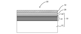
- FIG. 1 is a schematic view showing a cross section of a substrate with a multilayer reflective film according to this embodiment.
- the substrate 10 with a multilayer reflective film includes a substrate 12 and a multilayer reflective film 14 that reflects EUV light that is exposure light.
- the substrate 10 with a multilayer reflective film may include a protective film 18 for protecting the multilayer reflective film 14.
- the multilayer reflective film 14 is formed on the substrate 12, and the protective film 18 is formed on the multilayer reflective film 14.
- the substrate with a multilayer reflective film 10 has four or more reference marks that serve as references for defect positions.
- “on” a substrate or a film includes not only the case where the substrate or the film is in contact with the upper surface but also the case where the substrate or the film is not in contact with the upper surface. That is, “on” the substrate or film includes a case where a new film is formed above the substrate or film, a case where another film is interposed between the substrate and the film, and the like. .. In addition, “upward” does not necessarily mean an upper side in the vertical direction. The term "on top” merely indicates a relative positional relationship between the substrate and the film.
- the substrate 12 used in the substrate 10 with the multilayer reflective film of the present embodiment has a low heat within the range of 0 ⁇ 5 ppb / ° C. in order to prevent distortion of the absorber film pattern due to heat during exposure.
- Those having a coefficient of expansion are preferably used.
- As a material having a low coefficient of thermal expansion in this range for example, SiO 2 —TiO 2 glass, multi-component glass ceramics, etc. can be used.
- the main surface on the side of the substrate 12 where the transfer pattern (the absorber film pattern described later corresponds to this) is preferably processed to enhance the flatness.
- the flatness is preferably 0.1 ⁇ m or less, more preferably 0.05 ⁇ m or less, particularly preferably 0.05 ⁇ m or less in a 132 mm ⁇ 132 mm area of the main surface of the substrate 12 on the side where the transfer pattern is formed. It is preferably 0.03 ⁇ m or less.
- the main surface on the side opposite to the side on which the transfer pattern is formed is a surface fixed to the exposure device by an electrostatic chuck and has a flatness of 1 ⁇ m or less, more preferably 0, in an area of 142 mm ⁇ 142 mm. It is 0.5 ⁇ m or less, particularly preferably 0.03 ⁇ m or less.
- the flatness is a value representing the warp (deformation amount) of the surface indicated by TIR (Total Indicated Reading), and the plane determined by the least squares method with the substrate surface as a reference is the focal plane. It is the absolute value of the height difference between the highest position of the substrate surface above the plane and the lowest position of the substrate surface below the focal plane.
- the surface roughness of the main surface of the substrate 12 on which the transfer pattern is formed is preferably 0.1 nm or less in terms of root mean square roughness (RMS).
- the surface roughness can be measured with an atomic force microscope.
- the substrate 12 preferably has high rigidity in order to prevent the film (such as the multilayer reflective film 14) formed thereon from being deformed due to film stress.
- the substrate 12 preferably has a high Young's modulus of 65 GPa or more.
- the substrate 10 with a multilayer reflective film includes a substrate 12 and a multilayer reflective film 14 formed on the substrate 12.
- the multilayer reflective film 14 is, for example, a multilayer film in which elements having different refractive indexes are periodically stacked.
- the multilayer reflective film 14 has a function of reflecting EUV light.
- the multilayer reflective film 14 includes a thin film of a light element or its compound (high refractive index layer) which is a high refractive index material and a thin film of a heavy element or its compound (low refractive index layer) which is a low refractive index material. ) And are alternately laminated for about 40 to 60 cycles.
- the high refractive index layer and the low refractive index layer may be laminated in this order for a plurality of cycles from the substrate 12 side. In this case, one (high refractive index layer / low refractive index layer) laminated structure has one cycle.
- a plurality of low refractive index layers and a plurality of high refractive index layers may be laminated in this order from the substrate 12 side in this order.
- one (low refractive index layer / high refractive index layer) laminated structure has one cycle.
- the uppermost layer of the multilayer reflective film 14, that is, the surface layer of the multilayer reflective film 14 opposite to the substrate 12 is preferably a high refractive index layer.
- the uppermost layer is the low refractive index layer.
- the low-refractive index layer is the surface of the multi-layer reflective film 14
- the low-refractive index layer is easily oxidized and the reflectivity of the multi-layer reflective film is reduced.
- a high refractive index layer is formed.
- the uppermost layer is the high refractive index layer. In that case, the uppermost high refractive index layer becomes the surface of the multilayer reflective film 14.
- the high refractive index layer may be a layer containing Si.
- the high refractive index layer may include a simple substance of Si or may include a Si compound.
- the Si compound may include Si and at least one element selected from the group consisting of B, C, N, and O.
- the low refractive index material is at least one element selected from the group consisting of Mo, Ru, Rh, and Pt, or at least selected from the group consisting of Mo, Ru, Rh, and Pt. Alloys containing one element can be used.
- a Mo / Si multilayer film in which Mo films and Si films are alternately laminated for about 40 to 60 cycles can be preferably used.
- the multilayer reflective film used in the EUV light region for example, Ru / Si periodic multilayer film, Mo / Be periodic multilayer film, Mo compound / Si compound periodic multilayer film, Si / Nb periodic multilayer film, Si / A Mo / Ru periodic multilayer film, a Si / Mo / Ru / Mo periodic multilayer film, a Si / Ru / Mo / Ru periodic multilayer film, or the like can be used.
- the material of the multilayer reflective film can be selected in consideration of the exposure wavelength.
- the reflectance of such a multilayer reflective film 14 alone is, for example, 65% or more.
- the upper limit of the reflectance of the multilayer reflective film 14 is 73%, for example.
- the thickness and period of the layers included in the multilayer reflective film 14 can be selected so as to satisfy Bragg's law.
- the multilayer reflective film 14 can be formed by a known method.
- the multilayer reflective film 14 can be formed by, for example, an ion beam sputtering method.
- the multilayer reflection film 14 is a Mo / Si multilayer film
- a Mo film having a thickness of about 3 nm is formed on the substrate 12 by using an Mo target by an ion beam sputtering method.
- a Si target is used to form a Si film having a thickness of about 4 nm.
- the multilayer reflective film 14 in which Mo / Si films are laminated for 40 to 60 cycles.
- the surface layer of the multilayer reflective film 14 on the side opposite to the substrate 12 is a layer containing Si (Si film).
- the thickness of the Mo / Si film for one cycle is 7 nm.
- the substrate 10 with a multilayer reflective film of the present embodiment may include a protective film 18 formed on the multilayer reflective film 14.
- the protective film 18 has a function of protecting the multilayer reflective film 14 at the time of patterning or pattern modification of the absorber film described later.
- the protective film 18 is provided, for example, between the multilayer reflective film 14 and the absorber film.
- the material of the protective film 18 examples include Ru, Ru- (Nb, Zr, Y, B, Ti, La, Mo, Co or Re) compounds, Si- (Ru, Rh, Cr or B) compounds, Si, Materials such as Zr, Nb, La and B can be used. Further, a compound in which nitrogen, oxygen, or carbon is added to these can be used. Of these, when a material containing ruthenium (Ru) is applied, the reflectance characteristic of the multilayer reflective film becomes better.
- the material of the protective film 18 is preferably Ru or a Ru- (Nb, Zr, Y, B, Ti, La, Mo, Co or Re) compound.
- the thickness of the protective film 18 is, for example, 1 nm to 5 nm.
- the protective film 18 can be formed by a known method.
- the protective film 18 can be formed by, for example, a magnetron sputtering method or an ion beam sputtering method.
- the substrate 10 with a multilayer reflection film may further have a back surface conductive film on the main surface of the substrate 12 opposite to the side where the multilayer reflection film 14 is formed.
- the back surface conductive film is used when the substrate 10 with a multilayer reflective film or the reflective mask blank is attracted by an electrostatic chuck.
- the substrate 10 with a multilayer reflective film may include a base film formed between the substrate 12 and the multilayer reflective film 14.
- the base film is formed for the purpose of improving the smoothness of the surface of the substrate 12, for example.
- the base film is formed for the purpose of, for example, reducing defects, improving the reflectance of the multilayer reflective film, and correcting the stress of the multilayer reflective film.
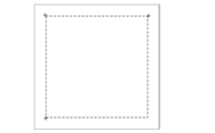
- FIG. 2 is a plan view of the substrate 10 with a multilayer reflective film according to this embodiment.
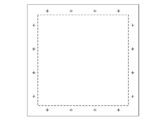
- reference marks 20 are formed in the vicinity of the four corners of the substantially rectangular substrate 10 with a multilayer reflective film.
- the reference mark 20 is a mark used as a reference for the defect position in the defect information.
- FIG. 2 shows an example in which four reference marks 20 are formed, the number of reference marks 20 may be four or more. Further, the four or more reference marks 20 may be arranged on at least two axes.
- an absorber film pattern is formed in a region inside the broken line A (a region of 132 mm ⁇ 132 mm) when a reflective mask is manufactured. In the region outside the broken line A, the absorber film pattern is not formed when the reflective mask is manufactured.
- the reference mark 20 is preferably formed in a region where the absorber film pattern is not formed, that is, in the region above the broken line A or outside the broken line A.
- the reference mark 20 has a substantially cross shape.
- the widths W1 and W2 of the reference mark 20 having a substantially cross shape are, for example, 200 nm or more and 10 ⁇ m or less.
- the length L of the reference mark 20 is, for example, 100 ⁇ m or more and 1500 ⁇ m or less.
- FIG. 2 shows an example of the reference mark 20 having a substantially cross shape, the shape of the reference mark 20 is not limited to this.
- the shape of the reference mark 20 may be, for example, a substantially L shape, a circle, a triangle, a quadrangle, or the like in plan view.
- the cross-sectional shape of the reference mark 20 is, for example, concave.
- concave as used herein means that when the cross section of the substrate 10 with a multilayer reflection film (a cross section perpendicular to the main surface of the substrate 10 with a multilayer reflection film) is viewed, the reference mark 20 faces downward, for example, a step shape or It means that it is formed so as to be concave in a curved shape.
- the depth D of the reference mark 20 formed in a concave shape is preferably 30 nm or more.
- the depth D of the reference mark 20 may be the depth at which the substrate 12 is exposed, but is preferably 100 nm or less, and more preferably 50 nm or less. When the depth D is small, the effect of the present invention can be obtained more significantly.
- the depth D means the distance in the vertical direction from the surface of the substrate with a multilayer reflective film 10 to the deepest position of the bottom of the reference mark 20.
- the method of forming the reference mark 20 is not particularly limited.
- the reference mark 20 can be formed, for example, by laser processing on the surface of the substrate 10 with a multilayer reflective film. At this time, the reference mark 20 may be formed after the multilayer reflective film 14 is formed, and then the protective film 18 may be formed. Alternatively, the multilayer reflective film 14 and the protective film 18 may be formed and then the reference mark 20 is formed. It may be formed.
- the laser processing conditions are as follows, for example.
- Laser power 1 to 120 mW
- Scan speed 0.1-20 mm / s
- Pulse frequency 1 to 100 MHz Pulse width: 3ns to 1000s
- the laser used for laser processing the reference mark 20 may be continuous wave or pulse wave.
- the width W of the reference mark 20 can be made smaller than that of the continuous wave even if the depth D of the reference mark 20 is about the same. Therefore, when the pulse wave is used, it is possible to form the reference mark 20 which has a higher contrast than the continuous wave and is easily detected by the defect inspection device or the electron beam drawing device.
- the method of forming the reference mark 20 is not limited to the laser.
- the reference mark 20 can be formed by, for example, a photolithography method, an FIB (focused ion beam), a processing mark obtained by scanning with a diamond stylus, an indentation by a minute indenter, or an embossing by an imprint method.
- FIB focused ion beam
- the cross-sectional shape of the reference mark 20 is not limited to the concave shape.
- the cross-sectional shape of the reference mark 20 may be a convex shape protruding upward.
- the reference mark 20 has a convex cross-sectional shape, it can be formed by partial film formation by FIB or sputtering.
- the height H of the reference mark 20 formed in a convex shape is preferably 30 nm or more.
- the height H of the reference mark 20 is preferably 100 nm or less, and more preferably 50 nm or less. When the height H is small, the effect of the present invention can be more remarkably obtained.
- the height H means the distance in the vertical direction from the surface of the substrate 10 with the multilayer reflective film to the highest position of the reference mark 20.
- the defect inspection apparatus acquires the reference mark 20 and the coordinates of the defect with high accuracy.
- an absorber film is formed on the protective film 18 of the substrate 10 with the multilayer reflective film.
- a resist film is formed on the absorber film.
- a hard mask film (or an etching mask film) may be formed between the absorber film and the resist film.
- the concave reference mark 20 formed on the substrate 10 with the multilayer reflective film is transferred to the absorber film and the resist film.
- the concave reference mark 20 formed on the substrate 10 with the multilayer reflection film is transferred to the absorber film, the hard mask film and the resist film. ..
- the reference mark 20 formed on the substrate 10 with the multilayer reflective film needs to have a high contrast that can be detected by the defect inspection apparatus.
- a mask substrate / blank defect inspection device "MAGICSM7360" for EUV exposure made by Lasertec which has an inspection light source wavelength of 266 nm
- an EUV made by KLA-Tencor which has an inspection light source wavelength of 193 nm
- a mask / blank defect inspection apparatus “Teron 600 series, for example, Teron 610” or an ABI (Actinic Blank Inspection) apparatus whose inspection light source wavelength is the same as the exposure light source wavelength of 13.5 nm can be used.
- the reference mark 20 transferred to the absorber film and / or the resist film thereon needs to have a high contrast that can be detected by the coordinate measuring device and / or the electron beam drawing device.
- the coordinate measuring device for example, "LAMS-IPRO4" manufactured by KLA-Tencor Co., which measures coordinates with a laser having a wavelength of 365 nm, "PROVE” manufactured by Carl Zeiss Co., which measures coordinates with a laser having a wavelength of 193 nm, and / or A coordinate measuring device mounted on the electron beam drawing apparatus can be used.
- the effect of the present invention can be more remarkably obtained when the coordinate measuring device has a wavelength different from that of the above-described defect inspection device.
- the reference mark 20 can be used as an FM (fiducial mark), for example.
- the FM is a mark used as a reference for defect coordinates when a pattern is drawn by an electron beam drawing apparatus.
- the FM usually has a cross shape as shown in FIG.
- the reference mark 20 By using the reference mark 20 as an FM, defect coordinates can be managed with high accuracy.
- the reference mark 20 transferred to the resist film is used as an FM that is a reference for the defect position.
- the defect coordinates acquired by the defect inspection apparatus can be converted into the coordinate system of the electron beam drawing apparatus by detecting the FM with the electron beam drawing apparatus.
- the drawing data of the pattern drawn by the electron beam drawing apparatus can be corrected so that the defect is arranged under the absorber film pattern. By correcting the writing data, it is possible to reduce the influence of defects on the finally manufactured reflective mask.
- the reference mark 20 can also be used as an AM (alignment mark).
- AM is a mark that can be used as a reference for defect coordinates when inspecting a defect on the substrate 10 with a multilayer reflection film by a defect inspection device.
- AM is not directly used when drawing a pattern by an electron beam drawing apparatus.
- the shape of the AM in plan view is, for example, a circle, a quadrangle, or a cross.
- the FM is formed on the laminated film described later on the substrate 10 with the multilayer reflective film.
- the AM is transferred to the laminated film, but the detection accuracy of the AM can be improved by partially removing the laminated film on the AM.
- AM can be detected by a defect inspection device and a coordinate measuring device.
- the FM can be detected by the coordinate measuring device and the electron beam drawing device. Since both AM and FM can be detected by the coordinate measuring device, their relative positional relationship can be managed with high accuracy. Therefore, it is possible to highly accurately convert the AM-based defect coordinates acquired by the defect inspection apparatus into the FM-based defect coordinates used in the electron beam drawing apparatus.
- the number of AMs is larger than the number of FMs.
- the substrate 10 with a multilayer reflection film of the present embodiment has four or more (for example, N) reference marks 20 (four reference marks in FIG. 2) that serve as references for the positions of defects in the substrate 10 with a multilayer reflection film.
- the value of 3 ⁇ obtained by the following procedures (1) to (5) is less than 50 nm.
- the defect inspection apparatus having the first coordinate system acquires the first defect coordinate of the defect in the substrate 10 with the multilayer reflection film and the first reference mark coordinate of the reference mark 20.
- the coordinate measuring instrument having the second coordinate system acquires the second defect coordinate of the defect and the second reference mark coordinate of the reference mark 20 in the substrate 10 with the multilayer reflection film.
- the defect inspection apparatus obtains the first defect coordinates of the defect in the multilayer reflection film coated substrate 10 and the first reference mark coordinates (x, y) of the N reference marks 20. ..
- the defect inspection device for example, the defect inspection device described above can be used.
- the number of defects for obtaining the value of 3 ⁇ is preferably 3 or more, more preferably 9 or more, and further preferably 15 or more.
- the variation in the size of the N reference marks is small.
- the size of the N reference marks is preferably within ⁇ 5% of their average value, and more preferably within ⁇ 3%.
- the “size” here means, for example, the area of the reference mark in plan view.
- the coordinate measuring instrument acquires the second defect coordinate of the defect in the substrate 10 with the multilayer reflective film and the second reference mark coordinate (u, v) of the N reference marks 20. ..
- the coordinate measuring device for example, the above-mentioned coordinate measuring device can be used.
- the origin can be set at the center of the board.
- the origin may be set at an arbitrary corner of the substrate after acquiring edge coordinates at eight positions (two positions per side) on the four sides of the substrate and performing appropriate tilt correction.
- the coordinates of the reference mark 20 are determined by detecting the edges of the reference mark 20. It can be set at the intersection with the center line of.
- the conversion coefficient for converting the coordinates from the first coordinate system of the defect inspection device to the second coordinate system of the coordinate measuring device is calculated.
- linear conversion affine conversion
- an example of the method of calculating the transform coefficient using the affine transform will be described.
- this function ⁇ is a quadratic function, in order to find a, b, c that minimizes this function, this expression is partially differentiated by a, b, c.
- Partial differentiation is a function that represents the gradient of the error function, so the point where the partially differentiated function is 0 is the minimum value, which is also the minimum value. This can be expressed as follows.
- the conversion coefficient calculated in the above (3) is used to transfer the first defect coordinates acquired by the defect inspection device in the above (1) to the second coordinate system of the coordinate measuring instrument. Convert.
- a value of 3 ⁇ is set for the difference between the second defect coordinate acquired by the coordinate measuring instrument in the above (2) and the third defect coordinate converted in the above (4).
- the difference between the second defect coordinates “actually” acquired by the coordinate measuring device and the third defect coordinate converted into the second coordinate system of the coordinate measuring device using the conversion coefficient is 3 ⁇ .
- Find the value. 3 ⁇ is three times the standard deviation ⁇ . The fact that 3 ⁇ is small means that the conversion accuracy from the first coordinate system of the defect inspection apparatus to the second coordinate system of the coordinate measuring instrument is high.
- the second defect coordinate acquired by the coordinate measuring instrument in (2) above is (s j , t j ), and the third defect coordinate converted into the second coordinate system of the coordinate measuring instrument in (4) above. If the defect coordinates of (S j , T j ) are (S j , T j ), the difference between these coordinates is (s j -S j , t j -T j ). In this case, the value of 3 ⁇ can be obtained by calculating the standard deviation ⁇ of j pieces of data for each of the x-coordinate and the y-coordinate.
- the value of ⁇ can be obtained by the least squares method by applying the result obtained by actually measuring the number of reference marks 20 and measuring 3 ⁇ to the above equation (1).
- the number of reference marks 20 increases, the conversion accuracy of defect coordinates can be improved, and the number of reference marks 20 can be determined based on a desired 3 ⁇ .
- the number of reference marks 20 is preferably 4 or more, and 3 ⁇ can be set to less than 50 nm. Further, the number of reference marks 20 is more preferably 8 or more, and 3 ⁇ can be set to less than 25 nm. The number of reference marks 20 is more preferably 16 or more, and 3 ⁇ can be set to less than 20 nm. Further, from the viewpoint of increasing the number of processes for forming the reference marks 20 and increasing the number of defects when the number of the reference marks 20 is too large, the number of the reference marks 20 is preferably 100 or less. Further, when the number of reference marks 20 exceeds 60, the decrease width of 3 ⁇ tends to be small, and therefore the number of reference marks 20 is more preferably 60 or less.
- the value of 3 ⁇ obtained by the above steps (1) to (5) is less than 50 nm.
- the value of 3 ⁇ is less than 50 nm for both the x-coordinate and y-coordinate data.
- the conversion accuracy from the first coordinate system of the defect inspection apparatus to the second coordinate system of the coordinate measuring device can be improved.
- a user who is provided with the substrate with a multilayer reflective film 10 can collate the defect position specified by the defect inspection device with the drawing data with high accuracy, and in the finally manufactured reflective mask. Defects can be surely reduced.
- the second embodiment uses another substrate with a multilayer reflection film to obtain the correspondence between the number of reference marks and 3 ⁇ , and to provide the multilayer reflection having the number of reference marks determined based on the correspondence. It is different from the first embodiment in that it is a substrate with a film. Other than that, it is the same as the first embodiment. That is, the substrate 10 with a multilayer reflection film of the present embodiment is provided with the reference mark 20 that serves as a reference for the position of a defect in the substrate 10 with a multilayer reflection film, and the number of the reference marks 20 is determined by the following procedure (1 )-(7).
- (1) Obtain a first defect coordinate of a defect and a first reference mark coordinate of the reference mark in another substrate with a multilayer reflection film having a plurality of reference marks by the defect inspection device having the first coordinate system. To do.
- (2) The coordinate measuring instrument having the second coordinate system acquires the second defect coordinate of the defect and the second reference mark coordinate of the reference mark in the another multilayer reflective film coated substrate.
- (3) A conversion coefficient for converting the coordinates from the first coordinate system to the second coordinate system is calculated based on the first reference mark coordinates and the second reference mark coordinates.
- the first defect coordinates acquired by the defect inspection apparatus in (1) above can be converted into a third coordinate system based on the second coordinate system. Convert to the defect coordinates of.
- steps (1) to (5) are the same as the steps (1) to (5) of the first embodiment, except that another substrate with a multilayer reflective film is used.
- Defects in another substrate with a multilayer reflective film may be real defects or programmed defects.
- another substrate with a multilayer reflection film may be one substrate with a multilayer reflection film on which N reference marks are formed.
- the above steps (1) to (6) are performed on one substrate with a multilayer reflection film to obtain the correspondence between the number of reference marks and 3 ⁇ , and the above correspondence is performed in step (7).
- the number of reference marks is determined based on the relationship.
- the other substrate with a multilayer reflective film may be a plurality of substrates with a multilayer reflective film on which 4 to N different reference marks are formed.
- the above steps (1) to (5) are performed for each substrate with a multilayer reflective film, and in step (6), the correspondence between the number of reference marks and 3 ⁇ is acquired, and step (7) At, the number of reference marks is determined based on the correspondence.
- an optimum number of reference marks 20 is provided according to the shape of the reference mark, the defect inspection device and / or the coordinate measuring instrument.
- the substrate 10 with a multilayer reflective film can be obtained.
- FIG. 3 is a schematic view showing a cross section of the reflective mask blank 30 of this embodiment.
- the reflective mask blank 30 of the present embodiment can be manufactured by forming the laminated film 28 on the protective film 18 of the substrate 10 with the multilayer reflective film described above.
- the laminated film 28 may be an absorber film that absorbs EUV light.
- the laminated film 28 is an absorber film will be described.
- the absorber film has a function of absorbing EUV light which is exposure light. That is, the difference between the EUV light reflectance of the multilayer reflective film 14 (including the protective film 18 if there is a protective film 18) and the EUV light reflectance of the absorber film is a predetermined value or more. ..
- the reflectance of the absorber film for EUV light is 0.1% or more and 40% or less.
- the absorber film in the reflective mask blank 30 may be called a phase shift film.
- the absorber film preferably has a function of absorbing EUV light and can be removed by etching or the like. It is preferable that the absorber film can be etched by dry etching using a chlorine (Cl) -based gas or a fluorine (F) -based gas.
- the material of the absorber film is not particularly limited as long as the absorber film has such a function.
- the absorber film may have a single layer or a laminated structure.
- a plurality of films made of the same material may be laminated or a plurality of films made of different materials may be laminated.
- the material and composition may change stepwise and / or continuously in the thickness direction of the film.
- the material of the absorber film is preferably tantalum (Ta) alone or a material containing Ta, for example.
- the material containing Ta is, for example, a material containing Ta and B, a material containing Ta and N, a material containing Ta and B and at least one of O and N, a material containing Ta and Si, and Ta and Si.
- the absorber film is composed of, for example, Ni simple substance, Ni-containing material, Cr simple substance, Cr-containing material, Ru simple substance, Ru-containing material, Pd simple substance, Pd-containing material, Mo simple substance, and Mo-containing material. It may include at least one selected from the group.
- the thickness of the absorber film is preferably 30 nm to 100 nm.
- the absorber film can be formed by a known method such as a magnetron sputtering method or an ion beam sputtering method.
- the resist film 32 may be formed on the absorber film (laminated film 28). This aspect is shown in FIG. A resist pattern can be formed by drawing and exposing a pattern on the resist film 32 with an electron beam drawing apparatus and then performing a developing process. By performing dry etching on the absorber film using this resist pattern as a mask, a pattern can be formed on the absorber film.
- the laminated film 28 may include an absorber film and a hard mask film formed on the absorber film.
- the hard mask film is used as a mask when patterning the absorber film.
- the hard mask film and the absorber film are formed of materials having different etching selectivity.
- the material of the absorber film contains tantalum or a tantalum compound
- the material of the hard mask film preferably contains chromium or a chromium compound.
- the chromium compound preferably contains Cr and at least one selected from the group consisting of N, O, C, and H.
- the reflective mask blank 30 of the present embodiment includes four or more (for example, N) reference marks 20 that serve as a reference for the position of a defect on the substrate 10 with a multilayer reflective film.
- the absorber film (laminated film 28) formed on the substrate 10 with the multilayer reflective film may include a transfer reference mark to which the shape of the reference mark 20 is transferred.
- a transfer reference mark to which the shape of the reference mark 20 is transferred.
- the reference mark 20 is concave
- a concave transfer reference mark is formed on the absorber film (laminated film 28) formed thereon.
- a convex transfer reference mark is formed on the absorber film (laminated film 28) formed thereon.
- the reference mark 20 of this embodiment is the same as the reference mark 20 of the first embodiment.
- the transfer reference mark also has a substantially cross shape.
- the widths W1 'and W2' of the transfer reference mark having a substantially cross shape are, for example, 200 nm or more and 10 ⁇ m or less.
- the deviation ⁇ W ( (
- / W1) ⁇ 100) of the width W1 ′ (W2 ′) of the transfer reference mark from the width W1 (W2) of the reference mark 20 may be 10% or less. preferable.
- the deviation ⁇ W is 1% or more, and further the ⁇ W is 3% or more, the effect of the present invention can be more remarkably obtained.
- the length L ′ of the transfer reference mark is, for example, 100 ⁇ m or more and 1500 ⁇ m or less.
- the deviation ⁇ L ( (
- / L) ⁇ 100) of the length L ′ of the transfer reference mark from the length L of the reference mark 20 is preferably 1% or less. Further, when the deviation ⁇ L is 0.05% or more, the effect of the present invention can be more remarkably obtained.
- the transfer reference mark 20 when the reference mark 20 has a substantially circular shape, the transfer reference mark also has a substantially circular shape.
- the deviation (absolute value) of the diameter of the transfer reference mark from the diameter of the reference mark 20 is preferably 10% or less. Further, when the deviation is 1% or more, and further the deviation is 3% or more, the effect of the present invention is more remarkably obtained.
- the transfer reference mark 20 When the reference mark 20 is concave (convex), the transfer reference mark is also concave (convex).
- the depth D '(height H') of the transfer reference mark is preferably 30 nm or more.
- the depth D '(height H') is preferably 100 nm or less, and more preferably 50 nm or less.
- the deviation ⁇ D ( ⁇ H) of the depth D ′ (height H ′) of the transfer reference mark from the depth D (height H) of the reference mark 20 is preferably 10% or less. Further, when the deviation ⁇ D ( ⁇ H) is 0.05% or more, and further when ⁇ D ( ⁇ H) is 1% or more, the effect of the present invention can be more remarkably obtained.
- the value of 3 ⁇ obtained by the following procedures (1) to (5) may be less than 50 nm.
- the defect inspection apparatus having the first coordinate system acquires the first defect coordinate of the defect in the substrate 10 with the multilayer reflection film and the first reference mark coordinate of the reference mark 20.
- the coordinate measuring instrument having the second coordinate system acquires the second defect coordinate of the defect in the reflective mask blank 30 and the second reference mark coordinate of the transfer reference mark.
- the first defect coordinates acquired by the defect inspection apparatus in the above (1) are compared with the second coordinate system of the coordinate measuring machine as a reference. Convert to 3 defect coordinates.
- a value of 3 ⁇ is obtained.
- steps (1) to (5) are the same as the steps (1) to (5) in the substrate 10 with a multilayer reflective film according to the first embodiment described above, but in the step (2), the coordinate measuring device is used. The difference is that the second defect coordinate of the defect in the reflective mask blank 30 and the second reference mark coordinate of the transfer reference mark are acquired.
- the number of reference marks 20 can be determined based on the desired 3 ⁇ .
- the number of reference marks 20 is preferably 4 or more, and 3 ⁇ can be set to less than 50 nm. Further, the number of reference marks 20 is more preferably 8 or more, and 3 ⁇ can be set to less than 25 nm.
- the number of reference marks 20 is more preferably 16 or more, and 3 ⁇ can be set to less than 20 nm.
- the number of the reference marks 20 is preferably 100 or less. Further, when the number of reference marks 20 exceeds 60, the decrease width of 3 ⁇ tends to be small, and therefore the number of reference marks 20 is more preferably 60 or less.
- the value of 3 ⁇ obtained by the above steps (1) to (5) is less than 50 nm.
- the value of 3 ⁇ is less than 50 nm for both the x-coordinate and y-coordinate data.
- the conversion accuracy from the first coordinate system of the defect inspection apparatus to the second coordinate system of the coordinate measuring device can be improved.
- the user who is provided with the reflective mask blank 30 can collate the defect position specified by the defect inspection device with the drawing data with high accuracy, and the defect is produced in the finally manufactured reflective mask. Can be reliably reduced.
- the second fiducial mark coordinates of the transcription fiducial mark transferred to the absorber film (laminated film 28) are acquired in the above procedure (2). Since the FM on the absorber film is used as a reference when a pattern is drawn on the resist film by the electron beam drawing apparatus, by using the second reference mark coordinates of the transfer reference mark transferred to the absorber film, The coordinate conversion accuracy can be further improved. That is, when the absorber film (laminated film 28) is formed on the reference mark, the width and depth of the transfer reference mark transferred to the absorber film are changed, so that the position of the detected reference mark is changed. There are cases.
- the second reference mark coordinates of the transfer reference mark transferred to the absorber film are acquired, and the conversion coefficient is calculated based on the acquired second reference mark coordinates to consider the effect of the reference mark position deviation.
- the converted coefficient can be calculated. As a result, it becomes possible to further improve the coordinate conversion accuracy in the procedure (4).
- the fourth embodiment uses another substrate with a multilayer reflective film and another reflective mask blank having a laminated film on the other substrate with a multilayer reflective film to determine the number of reference marks and 3 ⁇ .
- the reflective mask blank 30 is different from the third embodiment in that the reflective mask blank 30 has the reference marks the number of which is obtained based on the corresponding relationship. Other than that, it is the same as the third embodiment.
- the reflective mask blank 30 of this embodiment includes the reference mark 20 that serves as a reference for the position of a defect in the substrate 10 with a multilayer reflective film.
- the absorber film (laminated film 28) formed on the substrate 10 with the multilayer reflection film includes a transfer reference mark to which the shape of the reference mark 20 is transferred.
- the number of the reference marks 20 is the number obtained in advance by the following procedures (1) to (7). (1) Obtain a first defect coordinate of a defect and a first reference mark coordinate of the reference mark in another substrate with a multilayer reflection film having a plurality of reference marks by the defect inspection device having the first coordinate system. To do.
- a conversion coefficient for converting the coordinates from the first coordinate system to the second coordinate system is calculated based on the first reference mark coordinates and the second reference mark coordinates.
- the first defect coordinates acquired by the defect inspection apparatus in (1) above can be converted into a third coordinate system based on the second coordinate system. Convert to the defect coordinates of.
- the steps (1) to (5) are the same as the steps (1) to (5) of the third embodiment, except that another substrate with a multilayer reflective film and another reflective mask blank are used. is there.
- Another multilayer reflective film coated substrate is the same as that of the third embodiment.
- Another reflective mask blank has a plurality of transfer reference marks to which the reference marks formed on another substrate with a multilayer reflective film are transferred.
- the number of reference marks is obtained using another substrate with a multilayer reflective film and another reflective mask blank, the shape of the reference mark, the shape of the transfer reference mark, the defect inspection device and / or the coordinate measuring instrument. According to the above, it is possible to obtain the substrate 10 with a multilayer reflective film having the optimum number of reference marks 20.
- the reflective mask blank 30 of this embodiment can be used to manufacture the reflective mask 40 of this embodiment.
- a method for manufacturing the reflective mask 40 will be described.
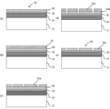
- FIG. 4 is a schematic view showing a method of manufacturing the reflective mask 40.
- a reflective mask blank 30 having the absorber film (laminated film 28) is prepared (FIG. 4A).
- the resist film 32 is formed on the absorber film (FIG. 4B).
- a pattern is drawn on the resist film 32 by an electron beam drawing apparatus, and a development / rinse process is performed to form a resist pattern 32a (FIG. 4C).
- the absorber film (laminated film 28) is dry-etched. As a result, the portion of the absorber film that is not covered with the resist pattern 32a is etched to form the absorber film pattern 28a (FIG. 4D).
- etching gas for example, chlorine-based gas such as Cl 2 , SiCl 4 , CHCl 3 and CCl 4 , a mixed gas containing these chlorine-based gas and O 2 in a predetermined ratio, chlorine-based gas and He are predetermined.
- the resist pattern 32a is removed with, for example, a resist stripping solution.
- the reflective mask 40 of the present embodiment is obtained by performing a wet cleaning process using an acidic or alkaline aqueous solution (FIG. 4E).
- a transfer pattern can be formed on the semiconductor substrate by lithography using the reflective mask 40 of this embodiment. This transfer pattern has a shape obtained by transferring the absorber film pattern 28a of the reflective mask 40.
- a semiconductor device can be manufactured by forming a transfer pattern on the semiconductor substrate using the reflective mask 40.
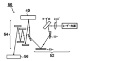
- FIG. 5 shows the pattern transfer device 50.
- the pattern transfer device 50 includes a laser plasma X-ray source 52, a reflective mask 40, and a reduction optical system 54.
- An X-ray reflection mirror is used as the reduction optical system 54.
- the pattern reflected by the reflective mask 40 is normally reduced to about 1/4 by the reduction optical system 54.
- a wavelength band of 13 to 14 nm is used as the exposure wavelength, and it is preset so that the optical path is in vacuum.
- the EUV light generated by the laser plasma X-ray source 52 is made incident on the reflective mask 40.
- the light reflected by the reflective mask 40 is transferred onto the semiconductor substrate 56 with resist via the reduction optical system 54.
- the light incident on the reflective mask 40 is absorbed by the absorber film and is not reflected at the portion where the absorber film pattern 28a is present. On the other hand, the light incident on the portion without the absorber film pattern 28a is reflected by the multilayer reflective film 14.
- the light reflected by the reflective mask 40 enters the reduction optical system 54.
- the light incident on the reduction optical system 54 forms a transfer pattern on the resist layer on the semiconductor substrate 56 with resist.
- a resist pattern can be formed on the semiconductor substrate 56 with resist.
- etching the semiconductor substrate 56 using the resist pattern as a mask for example, a predetermined wiring pattern can be formed on the semiconductor substrate.
- a semiconductor device is manufactured through these steps and other necessary steps.
- the reflective mask blank of this embodiment determines the number of FMs according to, for example, the second embodiment or the fourth embodiment described above.
- a method for manufacturing a reflective mask blank comprising: A step of forming a multilayer reflective film on the substrate to form a substrate with the multilayer reflective film; Forming a number of FMs determined on the basis of a desired 3 ⁇ on the surface of the substrate with a multilayer reflective film; Using the defect inspection apparatus, the first defect coordinates of the defect on the surface of the substrate with the multilayer reflection film and the first FM coordinates of the FM are acquired, and the first FM coordinates are used as a reference. Obtaining a defect map showing the first defect coordinates; A method of manufacturing a reflective mask blank, comprising: forming a laminated film having a transfer FM on which the FM is transferred, on the substrate having the multilayer reflective film.
- the user provided with the reflective mask blank and the defect map can collate the defect position specified by the defect inspection device with the drawing data with high accuracy based on the transfer FM, and finally manufactured. It is possible to reliably reduce defects in the reflective mask.
- the reflective mask blank of the present embodiment determines the number of AMs according to, for example, the second embodiment or the fourth embodiment described above.
- a method for manufacturing a reflective mask blank comprising: A step of forming a multilayer reflective film on the substrate to form a substrate with the multilayer reflective film; Forming a number of AMs determined on the basis of a desired 3 ⁇ on the surface of the substrate with the multilayer reflective film;
- the defect inspection apparatus is used to acquire the first defect coordinates of the defects on the surface of the substrate with the multilayer reflection film and the first AM coordinates of the AM, and thus the first AM coordinates are used as a reference.
- the user provided with the reflective mask blank and the second defect map can collate the defect position specified by the defect inspection apparatus with the drawing data with high accuracy based on FM, and finally, It is possible to surely reduce defects in the manufactured reflective mask.
- Example 1 An SiO 2 —TiO 2 glass substrate (6 inch square, thickness 6.35 mm) was prepared. The end face of this glass substrate was chamfered and ground, and then rough-polished with a polishing liquid containing cerium oxide abrasive grains. The glass substrate after these treatments was set in a carrier of a double-sided polishing machine, and precision polishing was performed under a predetermined polishing condition using an alkaline aqueous solution containing colloidal silica abrasive grains as a polishing liquid. After finishing the precision polishing, the glass substrate was washed.
- the surface roughness of the main surface of the obtained glass substrate was a root mean square roughness (RMS) of 0.10 nm or less.
- the flatness of the main surface of the obtained glass substrate was 30 nm or less in a measurement area of 132 mm ⁇ 132 mm.
- a multilayer reflective film was formed by periodically stacking a Mo film / Si film on the main surface of the glass substrate opposite to the side where the back surface conductive film was formed.
- a Mo target and a Si target were used, and a Mo film and a Si film were alternately laminated on the substrate by ion beam sputtering (using Ar).
- the Mo film has a thickness of 2.8 nm.
- the thickness of the Si film is 4.2 nm.
- the thickness of the Mo / Si film for one cycle is 7.0 nm.
- Such Mo / Si films were laminated for 40 cycles, and finally a Si film was formed to a thickness of 4.0 nm to form a multilayer reflective film.
- a protective film containing a Ru compound was formed on the multilayer reflective film. Specifically, a RuNb target (Ru: 80 atomic%, Nb: 20 atomic%) is used, and a protective film made of a RuNb film is formed on the multilayer reflective film by DC magnetron sputtering in an Ar gas atmosphere. did. The protective film had a thickness of 2.5 nm.
- An FM was formed on the protective film by laser processing.
- the laser processing conditions were as follows.
- Laser type Semiconductor laser with a wavelength of 405 nm
- Laser output 20 mW (continuous wave)
- Spot size 430nm ⁇
- the shape and dimensions of the FM were as follows. Shape: Almost cross-shaped Depth D: 40 nm Width W1, W2: 1 ⁇ m Length L: 1 mm
- the FM formation location was as shown in FIG. 6, and was outside the 132 mm ⁇ 132 mm effective area (area indicated by the broken line).
- the defect inspection device (ABI manufactured by Lasertec Co., Ltd.), the first defect coordinate of the defect in the substrate with the multilayer reflective film and the first FM coordinate of the FM were acquired.
- the number of defects was four.
- An absorber film was formed on the protective film of the substrate with the multilayer reflective film to manufacture a reflective mask blank. Specifically, an absorber film made of a laminated film of TaBN (thickness 56 nm) and TaBO (thickness 14 nm) was formed by DC magnetron sputtering.
- the TaBN film was formed using a TaB target by reactive sputtering in a mixed gas atmosphere of Ar gas and N 2 gas.
- the TaBO film was formed by reactive sputtering in a mixed gas atmosphere of Ar gas and O 2 gas using a TaB target.
- the transfer FM to which the FM was transferred was formed on the laminated film.
- the second defect coordinates of the defects in the reflective mask blank and the second FM coordinates of the transfer FM were acquired.
- a conversion coefficient for converting the coordinates from the first coordinate system of the defect inspection apparatus to the second coordinate system of the coordinate measuring instrument was calculated using the acquired first FM coordinates and second FM coordinates. ..
- the above-mentioned affine transformation formula was used to calculate the transformation coefficient.
- the first defect coordinates acquired by the defect inspection apparatus were converted into the second coordinate system of the coordinate measuring instrument to acquire the third defect coordinates.
- the difference between the third defect coordinate obtained by the conversion and the second defect coordinate obtained by the coordinate measuring instrument was obtained for each of the X coordinate and the Y coordinate.
- Such “difference” absolute value
- ⁇ and 3 ⁇ of this “difference” were calculated.
- 3 ⁇ was 24.2 nm in X coordinate and 23.3 nm in Y coordinate, and both were less than 50 nm.
- a resist film was formed on the absorber film of the reflective mask blank manufactured above.
- a pattern was drawn on the resist film using an electron beam drawing apparatus. When drawing a pattern, four transfer FMs were used as a reference for defect coordinates. After drawing the pattern, a predetermined development process was performed to form a resist pattern on the absorber film.
- a pattern was formed on the absorber film using the resist pattern as a mask. Specifically, the upper TaBO film was dry-etched with a fluorine-based gas (CF 4 gas), and then the lower TaBN film was dry-etched with a chlorine-based gas (Cl 2 gas).
- CF 4 gas fluorine-based gas
- Cl 2 gas chlorine-based gas
- the reflective mask according to Example 1 was obtained by removing the resist pattern remaining on the absorber film pattern with hot sulfuric acid.
- a mask defect inspection apparatus Teon 600 series manufactured by KLA-Tencor
- Example 2 A substrate with a multilayer reflective film and a reflective mask blank were manufactured in the same manner as in Example 1 except that the number of FMs was changed from 8 to 16.
- the FM formation location was as shown in FIG. 9, and was outside the 132 mm ⁇ 132 mm effective area (area indicated by the broken line).
- 3 ⁇ was calculated in the same manner as in Example 1. As a result, in the case of 16 FMs, 3 ⁇ was X coordinate of 18.2 nm and Y coordinate of 18.0 nm, and both were less than 50 nm.
- Example 2 Similar to Example 1, a reflection type mask of Example 2 was obtained by drawing a pattern on a resist film by an electron beam drawing device based on the position information of defects with the transfer FM as a reference.
- a mask defect inspection apparatus Teon 600 series manufactured by KLA-Tencor
- Example 3 A multilayer reflective film-coated substrate of Example 3 using the multilayer reflective film-coated substrate and the reflective mask blank having the eight FMs of Example 1 as another multilayer reflective film-coated substrate and another reflective mask blank. And a reflective mask blank was produced. From the correspondence between the number of FMs obtained in Example 1 and 3 ⁇ , the number of FMs with 3 ⁇ of less than 30 nm was calculated, and the number of FMs was set to 7. In the same manner as in Example 1, the multilayer reflective film and the protective film were formed on the main surface of the glass substrate opposite to the side where the back surface conductive film was formed. FM was formed on the protective film by laser processing, and a substrate with a multilayer reflective film having 7 FMs was manufactured. The shape and dimensions of the FM were as follows. Shape: Almost cross-shaped Depth D: 40 nm Width W1, W2: 1 ⁇ m Length L: 1m
- Example 2 In the same manner as in Example 1, a defect inspection apparatus (ABI, manufactured by Lasertec Co., Ltd.) was used to obtain the first defect coordinates of the defects in the substrate with the multilayer reflective film and the first FM coordinates of the FM, A defect map showing the first defect coordinates with respect to the first FM coordinates was obtained. The number of defects was 5.
- Example 2 In the same manner as in Example 1, a laminated film in which the transfer FM was formed was formed on the protective film, and a reflective mask blank was produced.
- the deviation ⁇ D of the transfer FM depth D ′ from the FM depth D was almost zero.
- the deviations ⁇ W1 and ⁇ W2 of the transfer FM widths W1 ′ and W2 ′ from the FM widths W1 and W2 were 7%, respectively.
- the deviation ⁇ L of the transfer FM length L ′ from the FM length L was 0.1%.
- the second defect coordinates of the defects in the reflective mask blank and the second FM coordinates of the transfer FM were acquired. Similar to the first embodiment, the first defect coordinate is converted into the second coordinate system of the coordinate measuring instrument, and the third defect coordinate obtained by the conversion and the second defect coordinate obtained by the coordinate measuring instrument are converted. The difference from the defect coordinate was obtained for each of the X coordinate and the Y coordinate. As a result, 3 ⁇ was less than 30 nm.
- a reflective mask was manufactured in the same manner as in Example 1.
- a mask defect inspection apparatus Teon 600 series manufactured by KLA-Tencor
- Example 4 Based on the results of FIG. 8 described above, 28 AMs were calculated as the number of AMs having 3 ⁇ of less than 20 nm, and a substrate with a multilayer reflective film and a reflective mask blank of Example 4 were produced. In the same manner as in Example 1, the multilayer reflective film and the protective film were formed on the main surface of the glass substrate opposite to the side where the back surface conductive film was formed.
- AM was formed on the protective film by laser processing.
- the laser processing conditions were as follows.
- Laser type Semiconductor laser with a wavelength of 405 nm
- Laser output 20 mW (continuous wave)
- Spot size 430nm ⁇
- the shape and dimensions of the AM were as follows. Shape: almost circular Depth: 40 nm Diameter: 0.9 ⁇ m
- the AM formation location was as shown in FIG. 10, and was outside the 132 mm ⁇ 132 mm effective area (the area indicated by the broken line).
- the first defect coordinates of the defects in the substrate with the multilayer reflective film and the first AM coordinates of 28 AMs were acquired.
- An absorber film was formed on the protective film of the substrate with the multilayer reflective film to manufacture a reflective mask blank. Specifically, an absorber film made of a laminated film of TaBN (thickness 56 nm) and TaBO (thickness 14 nm) was formed by DC magnetron sputtering.
- the TaBN film was formed using a TaB target by reactive sputtering in a mixed gas atmosphere of Ar gas and N 2 gas.
- the TaBO film was formed by reactive sputtering in a mixed gas atmosphere of Ar gas and O 2 gas using a TaB target.
- 28 transfer AMs to which AMs were transferred were formed.
- the deviation ⁇ D of the transfer AM depth D ′ from the AM depth D was almost zero.
- the deviation of the diameter of the transferred AM from the diameter of the AM was 6%.
- FM was formed on the surface of the absorber film by FIB processing.
- the conditions for FIB processing were as follows. Accelerating voltage: 50kV Beam current value: 20pA
- the shape and dimensions of the FM were as follows. Shape: Almost cross-shaped Depth D: 70 nm Width W1, W2: 5 ⁇ m Length L: 1 mm
- LMS-IPRO4 manufactured by KLA-Tencor
- the first defect coordinates acquired by the defect inspection device were converted into the second coordinate system of the coordinate measuring instrument, and the third defect coordinates were acquired.
- a resist film was formed on the absorber film of the reflective mask blank manufactured above.
- a pattern was drawn on the resist film using an electron beam drawing apparatus.
- FM was used as a reference for defect coordinates.
- the relative positional relationship between the transfer AM and FM was acquired by a coordinate measuring device.
- the position information of the defect with AM as a reference was converted into the position information of the defect with FM as a reference.
- a pattern was drawn on the resist film by an electron beam drawing apparatus based on the position information of the defect based on the FM.
- a pattern was formed on the absorber film using the resist pattern as a mask. Specifically, the upper TaBO film was dry-etched with a fluorine-based gas (CF 4 gas), and then the lower TaBN film was dry-etched with a chlorine-based gas (Cl 2 gas).
- CF 4 gas fluorine-based gas
- Cl 2 gas chlorine-based gas
- the reflective mask according to Example 4 was obtained by removing the resist pattern remaining on the absorber film pattern with hot sulfuric acid.
- a mask defect inspection apparatus Teon 600 series manufactured by KLA-Tencor
- Example 1 A substrate with a multilayer reflective film and a reflective mask blank were manufactured in the same manner as in Example 1 except that the number of FMs was changed from 8 to 3.
- the FM formation location was as shown in FIG. 11, and was outside the 132 mm ⁇ 132 mm effective area (the area indicated by the broken line).
- a reflection type mask of Comparative Example 1 was obtained by drawing a pattern on a resist film by an electron beam drawing apparatus based on the position information of the defect based on the transfer FM.
- the obtained EUV reflective mask was inspected by a mask defect inspection device (Teron 600 series manufactured by KLA-Tencor), the accuracy of coordinate conversion was poor, and therefore the defect could not be hidden under the absorber film pattern. Defects were confirmed in the exposed areas of the multilayer reflective film.
Abstract
The present invention allows improvement in the accuracy of conversion from a coordinate system of a defect inspection device for detecting defects on a multilayer reflection film into a coordinate system of a device other than the defect inspection device. This multilayer reflection film-provided substrate includes reference marks, the number of which is predetermined through steps (1) to (7). In step (1), the defect inspection device acquires first defect coordinates of defects and first reference mark coordinates of reference marks on a different multilayer reflection film-provided substrate. In step (2), a coordinate measurement device acquires second defect coordinates of the defects and second reference mark coordinates of the reference marks on the different multilayer reflection film-provided substrate. In step (3), a conversion coefficient for performing coordinate conversion from a coordinate system of the defect inspection device into a coordinate system of the coordinate measurement device is calculated on the basis of the first reference mark coordinates and the second reference mark coordinates. In step (4), the first defect coordinates are converted into third defect coordinates with use of the conversion coefficient calculated in step (3). In step (5), the value of 3σ is obtained for the difference between the second defect coordinates and the third defect coordinates. In step (6), the correspondence relationship between the number of the reference marks and 3σ is acquired. In step (7), the number of the reference marks at which the value of 3σ becomes less than 50 nm, is determined.
Description
本発明は、多層反射膜付き基板、反射型マスクブランク、反射型マスクの製造方法、及び半導体装置の製造方法に関する。
The present invention relates to a substrate with a multilayer reflective film, a reflective mask blank, a reflective mask manufacturing method, and a semiconductor device manufacturing method.
近年における超LSIデバイスの高密度化、高精度化の更なる要求に伴い、極紫外(Extreme Ultra Violet、以下、EUVと称す)光を用いた露光技術であるEUVリソグラフィーが有望視されている。ここで、EUV光とは、軟X線領域又は真空紫外線領域の波長帯の光を指し、具体的には波長が0.2~100nm程度の光のことである。EUVリソグラフィーにおいて用いられるマスクとして、反射型マスクが提案されている。反射型マスクは、ガラスやシリコンなどの基板上に、露光光を反射する多層反射膜が形成され、その多層反射膜の上に露光光を吸収する吸収体膜パターンが形成されたものである。パターン転写を行う露光機において、それに搭載された反射型マスクに入射した光は、吸収体膜パターンのある部分では吸収され、吸収体膜パターンのない部分では多層反射膜により反射される。そして反射された光像が、反射光学系を介してシリコンウエハ等の半導体基板上に転写される。
EUV lithography, which is an exposure technology using extreme ultra violet (hereinafter referred to as EUV) light, is regarded as promising with the recent demand for higher density and higher precision of VLSI devices. Here, the EUV light refers to light in the wavelength band of the soft X-ray region or the vacuum ultraviolet region, specifically, light having a wavelength of about 0.2 to 100 nm. A reflective mask has been proposed as a mask used in EUV lithography. The reflective mask has a multilayer reflective film that reflects exposure light formed on a substrate such as glass or silicon, and an absorber film pattern that absorbs exposure light is formed on the multilayer reflective film. In an exposure machine that performs pattern transfer, light incident on a reflective mask mounted on the exposure machine is absorbed in a portion having an absorber film pattern and reflected by a multilayer reflective film in a portion having no absorber film pattern. Then, the reflected light image is transferred onto a semiconductor substrate such as a silicon wafer via a reflection optical system.
リソグラフィー工程での微細化に対する要求が高まることにより、リソグラフィー工程における課題が顕著になりつつある。その課題の1つが、リソグラフィー工程で用いられるマスクブランク用基板等の欠陥情報に関する問題である。
Due to the increasing demands for miniaturization in the lithography process, the problems in the lithography process are becoming more prominent. One of the problems is a problem regarding defect information of a mask blank substrate used in a lithography process.
従来は、ブランクス検査等において、基板の欠陥の存在位置を、基板センターを原点(0,0)とし、欠陥検査装置が管理する座標系を用いて、その原点からの距離で特定していた。このため、絶対値座標の基準が明確でなく、位置精度が低く、装置間でも検出のばらつきがあった。また、パターン描画時に、欠陥を避けてパターン形成用薄膜にパターニングする場合でも、μmオーダーでの欠陥の回避は困難であった。このため、パターンを転写する方向を変えたり、転写する位置をmmオーダーでラフにずらしたりして、欠陥を回避していた。
Conventionally, in the blanks inspection, etc., the position of the defect on the board is specified by the distance from the origin using the coordinate system managed by the defect inspection device with the board center as the origin (0, 0). For this reason, the reference of the absolute value coordinates is not clear, the position accuracy is low, and there are variations in detection among devices. Further, even when the pattern forming thin film is patterned while avoiding defects during pattern writing, it is difficult to avoid defects on the order of μm. For this reason, the pattern transfer direction is changed, or the transfer position is roughly shifted in the mm order to avoid defects.
このような状況下、例えばマスクブランク用基板に基準マークを形成し、基準マークを基準として欠陥の位置を特定することが提案されている。マスクブランク用基板に基準マークを形成することにより、装置毎に欠陥の位置を特定するための基準がずれることが防止される。
Under such circumstances, it has been proposed to form a reference mark on a mask blank substrate, for example, and specify the position of the defect based on the reference mark. By forming the reference mark on the mask blank substrate, it is possible to prevent the reference for specifying the position of the defect for each device from being deviated.
露光光としてEUV光を使用する反射型マスクにおいては、多層反射膜上の欠陥の位置を正確に特定することが特に重要である。なぜなら、多層反射膜に存在する欠陥は、修正がほとんど不可能である上に、転写パターン上で重大な位相欠陥となり得るためである。
In a reflective mask that uses EUV light as the exposure light, it is particularly important to accurately identify the position of the defect on the multilayer reflective film. The reason is that the defects existing in the multilayer reflective film are almost impossible to repair, and in addition, they can be serious phase defects on the transfer pattern.
多層反射膜上の欠陥の位置を正確に特定するためには、多層反射膜を形成した後に欠陥検査を行うことで、欠陥の位置情報を取得することが好ましい。そのためには、基板上に形成された多層反射膜に、基準マークを形成することが好ましい。
In order to accurately specify the position of the defect on the multilayer reflective film, it is preferable to obtain defect position information by performing a defect inspection after forming the multilayer reflective film. For that purpose, it is preferable to form the reference mark on the multilayer reflective film formed on the substrate.
特許文献1には、球相当直径で30nm程度の微小な欠陥の位置を正確に特定できるように、EUVリソグラフィー用反射型マスクブランク用基板等に、大きさが球相当直径で30~100nmの少なくとも3つのマークを形成することが開示されている。
In Patent Document 1, in order to accurately specify the position of a minute defect having a sphere-equivalent diameter of about 30 nm, a reflective mask blank substrate for EUV lithography having at least a sphere-equivalent diameter of 30 to 100 nm is used. Forming three marks is disclosed.
マスクブランクの欠陥データとデバイスパターンデータとを元に、欠陥が存在している箇所に吸収体膜パターンが形成されるように描画データを補正して、欠陥を軽減させる技術(Defect mitigation technology)が提案されている。このような技術を実現するために、例えば、多層反射膜上に吸収体膜が形成された反射型マスクブランクにおいて、吸収体膜上に形成されたレジスト膜に電子線描画機を用いてパターンを描画する際に、電子線描画機においても電子線で基準マークを検出し、検出した基準点に基づいて、補正・修正した描画データを元にパターンを描画することが行われる。
Based on the mask blank defect data and the device pattern data, the technology (Defect migration technology) that corrects the drawing data so that the absorber film pattern is formed at the location where the defect exists and reduces the defect Proposed. In order to realize such a technique, for example, in a reflective mask blank in which an absorber film is formed on a multilayer reflection film, a pattern is formed on the resist film formed on the absorber film by using an electron beam drawing machine. At the time of drawing, the electron beam writer also detects the reference mark with the electron beam and draws a pattern based on the corrected / corrected drawing data based on the detected reference point.
マスクブランクの欠陥データを取得するための欠陥検査装置の座標系は、電子線描画機の座標系と異なっている。このため、欠陥検査装置で取得した基準マーク及び欠陥のデータを用いて電子線描画を行う際には、当該データを電子線描画機の座標系に変換する必要がある。
The coordinate system of the defect inspection device for acquiring the defect data of the mask blank is different from the coordinate system of the electron beam writer. Therefore, when performing electron beam drawing using the reference mark and defect data acquired by the defect inspection apparatus, it is necessary to convert the data into the coordinate system of the electron beam drawing machine.
しかし、欠陥検査装置の座標系から電子線描画機の座標系への変換精度が悪いと、上述のDefect mitigation technologyを実施したときに、描画データの補正・修正を高精度で行うことができないという問題が生じる。
However, if the accuracy of conversion from the coordinate system of the defect inspection device to the coordinate system of the electron beam drawing machine is poor, it is impossible to correct and correct drawing data with high accuracy when the above-mentioned Defect migration technology is executed. The problem arises.
そこで、本発明は、多層反射膜上の欠陥を検出する欠陥検査装置の座標系から、それ以外の装置の座標系への変換精度を向上させることのできる多層反射膜付き基板、反射型マスクブランク、反射型マスクの製造方法、及び半導体装置の製造方法を提供することを目的とする。
Therefore, the present invention is a substrate with a multilayer reflective film and a reflective mask blank capable of improving the conversion accuracy from the coordinate system of a defect inspection device that detects defects on a multilayer reflective film to the coordinate system of other devices. It is an object of the present invention to provide a method for manufacturing a reflective mask and a method for manufacturing a semiconductor device.
本発明者らは、多層反射膜上の欠陥を検出する欠陥検査装置の座標系から、それ以外の装置の座標系への変換精度を向上させることについて鋭意研究を行った。その結果、欠陥位置の基準となる基準マークの個数と、座標変換精度との間に相関があることを見出し、本発明を完成させた。
The present inventors have earnestly studied to improve the accuracy of conversion from the coordinate system of the defect inspection device that detects defects on the multilayer reflective film to the coordinate system of other devices. As a result, they found that there is a correlation between the number of reference marks serving as the reference of the defect position and the coordinate conversion accuracy, and completed the present invention.
上記課題を解決するため、本発明は以下の構成を有する。
(構成1)
基板と、該基板上に形成されたEUV光を反射する多層反射膜とを有する多層反射膜付き基板であって、
前記多層反射膜付き基板における欠陥の位置の基準となる基準マークを備えており、
前記基準マークの個数は、以下の手順(1)~(7)によって予め求められた個数であることを特徴とする、多層反射膜付き基板。
(1)第1の座標系を有する欠陥検査装置によって、複数の基準マークを有する別の多層反射膜付き基板における欠陥の第1の欠陥座標、及び、基準マークの第1の基準マーク座標を取得する。
(2)第2の座標系を有する座標計測器によって、前記別の多層反射膜付き基板における前記欠陥の第2の欠陥座標、及び、前記基準マークの第2の基準マーク座標を取得する。
(3)前記第1の基準マーク座標及び前記第2の基準マーク座標に基づいて、前記第1の座標系から前記第2の座標系へ座標を変換するための変換係数を算出する。
(4)上記(3)で算出された変換係数を用いて、上記(1)において前記欠陥検査装置によって取得された前記第1の欠陥座標を、前記第2の座標系を基準とした第3の欠陥座標へ変換する。
(5)上記(2)において前記座標計測器によって取得された前記第2の欠陥座標と、上記(4)で変換された第3の欠陥座標との間の差について、3σの値を求める。
(6)基準マークの個数と3σとの対応関係を取得する。
(7)3σの値が、50nm未満となる基準マークの個数を決定する。 In order to solve the above problems, the present invention has the following configurations.
(Structure 1)
A substrate with a multilayer reflective film, comprising: a substrate; and a multilayer reflective film formed on the substrate for reflecting EUV light,
It is provided with a reference mark serving as a reference for the position of a defect in the substrate with the multilayer reflective film,
The multilayer reflective film coated substrate, wherein the number of the reference marks is the number previously determined by the following procedures (1) to (7).
(1) Obtain a first defect coordinate of a defect and a first reference mark coordinate of the reference mark in another substrate with a multilayer reflection film having a plurality of reference marks by the defect inspection device having the first coordinate system. To do.
(2) The coordinate measuring instrument having the second coordinate system acquires the second defect coordinate of the defect and the second reference mark coordinate of the reference mark in the another multilayer reflective film coated substrate.
(3) A conversion coefficient for converting the coordinates from the first coordinate system to the second coordinate system is calculated based on the first reference mark coordinates and the second reference mark coordinates.
(4) Using the conversion coefficient calculated in (3) above, the first defect coordinates acquired by the defect inspection apparatus in (1) above can be converted into a third coordinate system based on the second coordinate system. Convert to the defect coordinates of.
(5) For the difference between the second defect coordinates acquired by the coordinate measuring instrument in (2) above and the third defect coordinates converted in (4) above, a value of 3σ is obtained.
(6) Obtain the correspondence between the number of reference marks and 3σ.
(7) The number of reference marks having a value of 3σ of less than 50 nm is determined.
(構成2)
前記基準マークの個数は、8個以上である、構成1に記載の多層反射膜付き基板。 (Structure 2)
The multilayer reflective film-coated substrate according to Configuration 1, wherein the number of the reference marks is 8 or more.
前記基準マークの個数は、8個以上である、構成1に記載の多層反射膜付き基板。 (Structure 2)
The multilayer reflective film-coated substrate according to Configuration 1, wherein the number of the reference marks is 8 or more.
(構成3)
前記基準マークの個数は、16個以上である、構成1または構成2に記載の多層反射膜付き基板。 (Structure 3)
The substrate with a multilayer reflective film according toconfiguration 1 or 2, wherein the number of the reference marks is 16 or more.
前記基準マークの個数は、16個以上である、構成1または構成2に記載の多層反射膜付き基板。 (Structure 3)
The substrate with a multilayer reflective film according to
(構成4)
構成1から構成3のうちいずれかに記載の多層反射膜付き基板と、該多層反射膜付き基板上に形成された積層膜とを有する反射型マスクブランク。 (Structure 4)
A reflective mask blank comprising: the substrate with a multilayer reflective film according to any one of configurations 1 to 3; and a laminated film formed on the substrate with a multilayer reflective film.
構成1から構成3のうちいずれかに記載の多層反射膜付き基板と、該多層反射膜付き基板上に形成された積層膜とを有する反射型マスクブランク。 (Structure 4)
A reflective mask blank comprising: the substrate with a multilayer reflective film according to any one of configurations 1 to 3; and a laminated film formed on the substrate with a multilayer reflective film.
(構成5)
基板及び該基板上に形成されたEUV光を反射する多層反射膜を有する多層反射膜付き基板と、該多層反射膜付き基板上に形成された積層膜とを有する反射型マスクブランクであって、
前記多層反射膜付き基板は、該多層反射膜付き基板における欠陥の位置の基準となる基準マークを備えており、
前記積層膜は、前記基準マークが転写された転写基準マークを備えており、
前記基準マークの個数は、以下の手順(1)~(7)によって予め求められた個数であることを特徴とする、反射型マスクブランク。
(1)第1の座標系を有する欠陥検査装置によって、複数の基準マークを有する別の多層反射膜付き基板における欠陥の第1の欠陥座標、及び、基準マークの第1の基準マーク座標を取得する。
(2)第2の座標系を有する座標計測器によって、前記別の多層反射膜付き基板上に形成された積層膜を有する反射型マスクブランクにおける欠陥の第2の欠陥座標、及び、転写基準マークの第2の基準マーク座標を取得する。
(3)前記第1の基準マーク座標及び前記第2の基準マーク座標に基づいて、前記第1の座標系から前記第2の座標系へ座標を変換するための変換係数を算出する。
(4)上記(3)で算出された変換係数を用いて、上記(1)において前記欠陥検査装置によって取得された前記第1の欠陥座標を、前記第2の座標系を基準とした第3の欠陥座標へ変換する。
(5)上記(2)において前記座標計測器によって取得された前記第2の欠陥座標と、上記(4)で変換された第3の欠陥座標との間の差について、3σの値を求める。
(6)基準マークの個数と3σとの対応関係を取得する。
(7)3σの値が、50nm未満となる基準マークの個数を決定する。 (Structure 5)
A reflective mask blank comprising a substrate and a substrate with a multilayer reflective film having a multilayer reflective film formed on the substrate for reflecting EUV light, and a laminated film formed on the substrate with the multilayer reflective film,
The substrate with a multilayer reflective film is provided with a reference mark serving as a reference for the position of a defect in the substrate with a multilayer reflective film,
The laminated film includes a transfer reference mark to which the reference mark is transferred,
The reflective mask blank is characterized in that the number of the reference marks is the number determined in advance by the following steps (1) to (7).
(1) Obtain a first defect coordinate of a defect and a first reference mark coordinate of the reference mark in another substrate with a multilayer reflection film having a plurality of reference marks by the defect inspection device having the first coordinate system. To do.
(2) Second coordinate coordinates of defects in a reflective mask blank having a laminated film formed on another substrate having a multilayer reflective film and a transfer reference mark by a coordinate measuring instrument having a second coordinate system To obtain the second fiducial mark coordinates of.
(3) A conversion coefficient for converting the coordinates from the first coordinate system to the second coordinate system is calculated based on the first reference mark coordinates and the second reference mark coordinates.
(4) Using the conversion coefficient calculated in (3) above, the first defect coordinates acquired by the defect inspection apparatus in (1) above can be converted into a third coordinate system based on the second coordinate system. Convert to the defect coordinates of.
(5) For the difference between the second defect coordinates acquired by the coordinate measuring instrument in (2) above and the third defect coordinates converted in (4) above, a value of 3σ is obtained.
(6) Obtain the correspondence between the number of reference marks and 3σ.
(7) The number of reference marks having a value of 3σ of less than 50 nm is determined.
(構成6)
前記基準マークの個数は、8個以上である、構成5に記載の反射型マスクブランク。 (Structure 6)
6. The reflective mask blank according to configuration 5, wherein the number of the reference marks is 8 or more.
前記基準マークの個数は、8個以上である、構成5に記載の反射型マスクブランク。 (Structure 6)
6. The reflective mask blank according to configuration 5, wherein the number of the reference marks is 8 or more.
(構成7)
前記基準マークの個数は、16個以上である、構成5または構成6に記載の反射型マスクブランク。 (Structure 7)
7. The reflective mask blank according toconfiguration 5 or 6, wherein the number of the reference marks is 16 or more.
前記基準マークの個数は、16個以上である、構成5または構成6に記載の反射型マスクブランク。 (Structure 7)
7. The reflective mask blank according to
(構成8)
前記積層膜は、EUV光を吸収する吸収体膜を含む、構成4から構成7のうちいずれかに記載の反射型マスクブランク。 (Structure 8)
8. The reflective mask blank according to any one ofconfigurations 4 to 7, wherein the laminated film includes an absorber film that absorbs EUV light.
前記積層膜は、EUV光を吸収する吸収体膜を含む、構成4から構成7のうちいずれかに記載の反射型マスクブランク。 (Structure 8)
8. The reflective mask blank according to any one of
(構成9)
構成4または構成8に記載の反射型マスクブランクにおける前記積層膜に積層膜パターンを形成する工程を有する、反射型マスクの製造方法。 (Configuration 9)
9. A method of manufacturing a reflective mask, comprising the step of forming a laminated film pattern on the laminated film in the reflective mask blank according toStructure 4 or Structure 8.
構成4または構成8に記載の反射型マスクブランクにおける前記積層膜に積層膜パターンを形成する工程を有する、反射型マスクの製造方法。 (Configuration 9)
9. A method of manufacturing a reflective mask, comprising the step of forming a laminated film pattern on the laminated film in the reflective mask blank according to
(構成10)
構成9に記載の反射型マスクの製造方法によって製造された反射型マスクを使用して、半導体基板上に転写パターンを形成する工程を有する、半導体装置の製造方法。 (Configuration 10)
A method for manufacturing a semiconductor device, comprising the step of forming a transfer pattern on a semiconductor substrate using the reflective mask manufactured by the method for manufacturing a reflective mask according to configuration 9.
本発明によれば、多層反射膜上の欠陥を検出するための欠陥検査装置の座標系から、それ以外の装置の座標系への変換精度を向上させることのできる多層反射膜付き基板及び反射型マスクブランクを提供することができる。また、本発明によれば、これら多層反射膜付き基板又は反射型マスクブランクを使用し、これらの欠陥情報に基づき、描画データの修正を行なうことで欠陥を低減させた反射型マスクの製造方法及び半導体装置の製造方法を提供することができる。
ADVANTAGE OF THE INVENTION According to this invention, the board | substrate with a multilayer reflective film and reflective type which can improve the conversion precision from the coordinate system of the defect inspection apparatus for detecting the defect on a multilayer reflective film to the coordinate system of other apparatuses. A mask blank can be provided. Further, according to the present invention, a method for manufacturing a reflective mask in which defects are reduced by using these substrates with a multilayer reflective film or a reflective mask blank and correcting writing data based on the defect information thereof, and A method for manufacturing a semiconductor device can be provided.
(第1の実施形態)
以下、本発明の実施形態について詳細に説明する。
[多層反射膜付き基板]
図1は、本実施形態の多層反射膜付き基板の断面を示す模式図である。
図1に示すように、多層反射膜付き基板10は、基板12と、露光光であるEUV光を反射する多層反射膜14とを備えている。さらに、多層反射膜付き基板10は、多層反射膜14を保護するための保護膜18を備えてもよい。本実施形態では、基板12の上に多層反射膜14が形成されており、多層反射膜14の上に保護膜18が形成されている。後述するように、多層反射膜付き基板10は、欠陥位置の基準となる4個以上の基準マークを備えている。 (First embodiment)
Hereinafter, embodiments of the present invention will be described in detail.
[Substrate with multilayer reflective film]
FIG. 1 is a schematic view showing a cross section of a substrate with a multilayer reflective film according to this embodiment.
As shown in FIG. 1, thesubstrate 10 with a multilayer reflective film includes a substrate 12 and a multilayer reflective film 14 that reflects EUV light that is exposure light. Further, the substrate 10 with a multilayer reflective film may include a protective film 18 for protecting the multilayer reflective film 14. In this embodiment, the multilayer reflective film 14 is formed on the substrate 12, and the protective film 18 is formed on the multilayer reflective film 14. As will be described later, the substrate with a multilayer reflective film 10 has four or more reference marks that serve as references for defect positions.
以下、本発明の実施形態について詳細に説明する。
[多層反射膜付き基板]
図1は、本実施形態の多層反射膜付き基板の断面を示す模式図である。
図1に示すように、多層反射膜付き基板10は、基板12と、露光光であるEUV光を反射する多層反射膜14とを備えている。さらに、多層反射膜付き基板10は、多層反射膜14を保護するための保護膜18を備えてもよい。本実施形態では、基板12の上に多層反射膜14が形成されており、多層反射膜14の上に保護膜18が形成されている。後述するように、多層反射膜付き基板10は、欠陥位置の基準となる4個以上の基準マークを備えている。 (First embodiment)
Hereinafter, embodiments of the present invention will be described in detail.
[Substrate with multilayer reflective film]
FIG. 1 is a schematic view showing a cross section of a substrate with a multilayer reflective film according to this embodiment.
As shown in FIG. 1, the
なお、本明細書において、基板や膜の「上に」とは、その基板や膜の上面に接触する場合だけでなく、その基板や膜の上面に接触しない場合も含む。すなわち、基板や膜の「上に」とは、その基板や膜の上方に新たな膜が形成される場合や、その基板や膜との間に他の膜が介在している場合等を含む。また、「上に」とは、必ずしも鉛直方向における上側を意味するものではない。「上に」とは、基板や膜などの相対的な位置関係を示しているに過ぎない。
In this specification, “on” a substrate or a film includes not only the case where the substrate or the film is in contact with the upper surface but also the case where the substrate or the film is not in contact with the upper surface. That is, “on” the substrate or film includes a case where a new film is formed above the substrate or film, a case where another film is interposed between the substrate and the film, and the like. .. In addition, “upward” does not necessarily mean an upper side in the vertical direction. The term "on top" merely indicates a relative positional relationship between the substrate and the film.
<基板>
本実施形態の多層反射膜付き基板10に使用される基板12としては、EUV露光の場合、露光時の熱による吸収体膜パターンの歪みを防止するため、0±5ppb/℃の範囲内の低熱膨張係数を有するものが好ましく用いられる。この範囲の低熱膨張係数を有する素材としては、例えば、SiO2-TiO2系ガラス、多成分系ガラスセラミックス等を用いることができる。 <Substrate>
In the case of EUV exposure, thesubstrate 12 used in the substrate 10 with the multilayer reflective film of the present embodiment has a low heat within the range of 0 ± 5 ppb / ° C. in order to prevent distortion of the absorber film pattern due to heat during exposure. Those having a coefficient of expansion are preferably used. As a material having a low coefficient of thermal expansion in this range, for example, SiO 2 —TiO 2 glass, multi-component glass ceramics, etc. can be used.
本実施形態の多層反射膜付き基板10に使用される基板12としては、EUV露光の場合、露光時の熱による吸収体膜パターンの歪みを防止するため、0±5ppb/℃の範囲内の低熱膨張係数を有するものが好ましく用いられる。この範囲の低熱膨張係数を有する素材としては、例えば、SiO2-TiO2系ガラス、多成分系ガラスセラミックス等を用いることができる。 <Substrate>
In the case of EUV exposure, the
基板12の転写パターン(後述の吸収体膜パターンがこれに対応する)が形成される側の主表面は、平坦度を高めるために加工されることが好ましい。基板12の主表面の平坦度を高めることによって、パターンの位置精度や転写精度を高めることができる。例えば、EUV露光の場合、基板12の転写パターンが形成される側の主表面の132mm×132mmの領域において、平坦度が0.1μm以下であることが好ましく、更に好ましくは0.05μm以下、特に好ましくは0.03μm以下である。また、転写パターンが形成される側と反対側の主表面は、露光装置に静電チャックによって固定される面であって、その142mm×142mmの領域において、平坦度が1μm以下、更に好ましくは0.5μm以下、特に好ましくは0.03μm以下である。なお、本明細書において平坦度は、TIR(Total Indicated Reading)で示される表面の反り(変形量)を表す値で、基板表面を基準として最小二乗法で定められる平面を焦平面とし、この焦平面より上にある基板表面の最も高い位置と、焦平面より下にある基板表面の最も低い位置との高低差の絶対値である。
The main surface on the side of the substrate 12 where the transfer pattern (the absorber film pattern described later corresponds to this) is preferably processed to enhance the flatness. By increasing the flatness of the main surface of the substrate 12, the positional accuracy and transfer accuracy of the pattern can be improved. For example, in the case of EUV exposure, the flatness is preferably 0.1 μm or less, more preferably 0.05 μm or less, particularly preferably 0.05 μm or less in a 132 mm × 132 mm area of the main surface of the substrate 12 on the side where the transfer pattern is formed. It is preferably 0.03 μm or less. Further, the main surface on the side opposite to the side on which the transfer pattern is formed is a surface fixed to the exposure device by an electrostatic chuck and has a flatness of 1 μm or less, more preferably 0, in an area of 142 mm × 142 mm. It is 0.5 μm or less, particularly preferably 0.03 μm or less. In this specification, the flatness is a value representing the warp (deformation amount) of the surface indicated by TIR (Total Indicated Reading), and the plane determined by the least squares method with the substrate surface as a reference is the focal plane. It is the absolute value of the height difference between the highest position of the substrate surface above the plane and the lowest position of the substrate surface below the focal plane.
EUV露光の場合、基板12の転写パターンが形成される側の主表面の表面粗さは、二乗平均平方根粗さ(RMS)で0.1nm以下であることが好ましい。なお表面粗さは、原子間力顕微鏡で測定することができる。
In the case of EUV exposure, the surface roughness of the main surface of the substrate 12 on which the transfer pattern is formed is preferably 0.1 nm or less in terms of root mean square roughness (RMS). The surface roughness can be measured with an atomic force microscope.
基板12は、その上に形成される膜(多層反射膜14など)の膜応力による変形を防止するために、高い剛性を有していることが好ましい。特に、基板12は、65GPa以上の高いヤング率を有していることが好ましい。
The substrate 12 preferably has high rigidity in order to prevent the film (such as the multilayer reflective film 14) formed thereon from being deformed due to film stress. In particular, the substrate 12 preferably has a high Young's modulus of 65 GPa or more.
<多層反射膜>
多層反射膜付き基板10は、基板12と、基板12の上に形成された多層反射膜14とを備えている。多層反射膜14は、例えば、屈折率の異なる元素が周期的に積層された多層膜からなる。多層反射膜14は、EUV光を反射する機能を有している。 <Multilayer reflective film>
Thesubstrate 10 with a multilayer reflective film includes a substrate 12 and a multilayer reflective film 14 formed on the substrate 12. The multilayer reflective film 14 is, for example, a multilayer film in which elements having different refractive indexes are periodically stacked. The multilayer reflective film 14 has a function of reflecting EUV light.
多層反射膜付き基板10は、基板12と、基板12の上に形成された多層反射膜14とを備えている。多層反射膜14は、例えば、屈折率の異なる元素が周期的に積層された多層膜からなる。多層反射膜14は、EUV光を反射する機能を有している。 <Multilayer reflective film>
The
一般的には、多層反射膜14は、高屈折率材料である軽元素又はその化合物の薄膜(高屈折率層)と、低屈折率材料である重元素又はその化合物の薄膜(低屈折率層)とが交互に40~60周期程度積層された多層膜からなる。
多層反射膜14を形成するために、基板12側から高屈折率層と低屈折率層をこの順に複数周期積層してもよい。この場合、1つの(高屈折率層/低屈折率層)の積層構造が、1周期となる。
多層反射膜14を形成するために、基板12側から低屈折率層と高屈折率層をこの順に複数周期積層してもよい。この場合、1つの(低屈折率層/高屈折率層)の積層構造が、1周期となる。 In general, the multilayerreflective film 14 includes a thin film of a light element or its compound (high refractive index layer) which is a high refractive index material and a thin film of a heavy element or its compound (low refractive index layer) which is a low refractive index material. ) And are alternately laminated for about 40 to 60 cycles.
In order to form the multilayerreflective film 14, the high refractive index layer and the low refractive index layer may be laminated in this order for a plurality of cycles from the substrate 12 side. In this case, one (high refractive index layer / low refractive index layer) laminated structure has one cycle.
In order to form the multilayerreflective film 14, a plurality of low refractive index layers and a plurality of high refractive index layers may be laminated in this order from the substrate 12 side in this order. In this case, one (low refractive index layer / high refractive index layer) laminated structure has one cycle.
多層反射膜14を形成するために、基板12側から高屈折率層と低屈折率層をこの順に複数周期積層してもよい。この場合、1つの(高屈折率層/低屈折率層)の積層構造が、1周期となる。
多層反射膜14を形成するために、基板12側から低屈折率層と高屈折率層をこの順に複数周期積層してもよい。この場合、1つの(低屈折率層/高屈折率層)の積層構造が、1周期となる。 In general, the multilayer
In order to form the multilayer
In order to form the multilayer
なお、多層反射膜14の最上層、すなわち多層反射膜14の基板12と反対側の表面層は、高屈折率層であることが好ましい。基板12側から高屈折率層と低屈折率層をこの順に積層する場合は、最上層が低屈折率層となる。しかし、低屈折率層が多層反射膜14の表面である場合、低屈折率層が容易に酸化されることで多層反射膜の反射率が減少してしまうので、その低屈折率層の上に高屈折率層を形成する。一方、基板12側から低屈折率層と高屈折率層をこの順に積層する場合は、最上層が高屈折率層となる。その場合は、最上層の高屈折率層が、多層反射膜14の表面となる。
The uppermost layer of the multilayer reflective film 14, that is, the surface layer of the multilayer reflective film 14 opposite to the substrate 12 is preferably a high refractive index layer. When the high refractive index layer and the low refractive index layer are laminated in this order from the substrate 12 side, the uppermost layer is the low refractive index layer. However, when the low-refractive index layer is the surface of the multi-layer reflective film 14, the low-refractive index layer is easily oxidized and the reflectivity of the multi-layer reflective film is reduced. A high refractive index layer is formed. On the other hand, when the low refractive index layer and the high refractive index layer are laminated in this order from the substrate 12 side, the uppermost layer is the high refractive index layer. In that case, the uppermost high refractive index layer becomes the surface of the multilayer reflective film 14.
本実施形態において、高屈折率層は、Siを含む層であってもよい。高屈折率層は、Si単体を含んでもよく、Si化合物を含んでもよい。Si化合物は、Siと、B、C、N、及びOからなる群から選択される少なくとも1つの元素を含んでもよい。Siを含む層を高屈折率層として使用することによって、EUV光の反射率に優れた多層反射膜が得られる。
In the present embodiment, the high refractive index layer may be a layer containing Si. The high refractive index layer may include a simple substance of Si or may include a Si compound. The Si compound may include Si and at least one element selected from the group consisting of B, C, N, and O. By using the layer containing Si as the high refractive index layer, a multilayer reflective film having excellent EUV light reflectance can be obtained.
本実施形態において、低屈折率材料としては、Mo、Ru、Rh、及びPtからなる群から選択される少なくとも1つの元素、あるいは、Mo、Ru、Rh、及びPtからなる群から選択される少なくとも1つの元素を含む合金を使用することができる。
In the present embodiment, the low refractive index material is at least one element selected from the group consisting of Mo, Ru, Rh, and Pt, or at least selected from the group consisting of Mo, Ru, Rh, and Pt. Alloys containing one element can be used.
例えば、波長13~14nmのEUV光のための多層反射膜14としては、好ましくは、Mo膜とSi膜を交互に40~60周期程度積層したMo/Si多層膜を用いることができる。その他に、EUV光の領域で使用される多層反射膜として、例えば、Ru/Si周期多層膜、Mo/Be周期多層膜、Mo化合物/Si化合物周期多層膜、Si/Nb周期多層膜、Si/Mo/Ru周期多層膜、Si/Mo/Ru/Mo周期多層膜、Si/Ru/Mo/Ru周期多層膜などを用いることができる。露光波長を考慮して、多層反射膜の材料を選択することができる。
For example, as the multilayer reflective film 14 for EUV light having a wavelength of 13 to 14 nm, a Mo / Si multilayer film in which Mo films and Si films are alternately laminated for about 40 to 60 cycles can be preferably used. In addition, as the multilayer reflective film used in the EUV light region, for example, Ru / Si periodic multilayer film, Mo / Be periodic multilayer film, Mo compound / Si compound periodic multilayer film, Si / Nb periodic multilayer film, Si / A Mo / Ru periodic multilayer film, a Si / Mo / Ru / Mo periodic multilayer film, a Si / Ru / Mo / Ru periodic multilayer film, or the like can be used. The material of the multilayer reflective film can be selected in consideration of the exposure wavelength.
このような多層反射膜14の単独での反射率は、例えば65%以上である。多層反射膜14の反射率の上限は、例えば73%である。なお、多層反射膜14に含まれる層の厚み及び周期は、ブラッグの法則を満たすように選択することができる。
The reflectance of such a multilayer reflective film 14 alone is, for example, 65% or more. The upper limit of the reflectance of the multilayer reflective film 14 is 73%, for example. The thickness and period of the layers included in the multilayer reflective film 14 can be selected so as to satisfy Bragg's law.
多層反射膜14は、公知の方法によって形成できる。多層反射膜14は、例えば、イオンビームスパッタ法により形成できる。
The multilayer reflective film 14 can be formed by a known method. The multilayer reflective film 14 can be formed by, for example, an ion beam sputtering method.
例えば、多層反射膜14がMo/Si多層膜である場合、イオンビームスパッタ法により、Moターゲットを用いて、厚さ3nm程度のMo膜を基板12の上に形成する。次に、Siターゲットを用いて、厚さ4nm程度のSi膜を形成する。このような操作を繰り返すことによって、Mo/Si膜が40~60周期積層した多層反射膜14を形成することができる。このとき、多層反射膜14の基板12と反対側の表面層は、Siを含む層(Si膜)である。1周期のMo/Si膜の厚みは、7nmとなる。
For example, when the multilayer reflection film 14 is a Mo / Si multilayer film, a Mo film having a thickness of about 3 nm is formed on the substrate 12 by using an Mo target by an ion beam sputtering method. Next, a Si target is used to form a Si film having a thickness of about 4 nm. By repeating such an operation, it is possible to form the multilayer reflective film 14 in which Mo / Si films are laminated for 40 to 60 cycles. At this time, the surface layer of the multilayer reflective film 14 on the side opposite to the substrate 12 is a layer containing Si (Si film). The thickness of the Mo / Si film for one cycle is 7 nm.
<保護膜>
本実施形態の多層反射膜付き基板10は、多層反射膜14の上に形成された保護膜18を備えてもよい。保護膜18は、後述の吸収体膜のパターニングあるいはパターン修正の際に、多層反射膜14を保護する機能を有している。保護膜18は、例えば、多層反射膜14と吸収体膜との間に設けられる。 <Protective film>
Thesubstrate 10 with a multilayer reflective film of the present embodiment may include a protective film 18 formed on the multilayer reflective film 14. The protective film 18 has a function of protecting the multilayer reflective film 14 at the time of patterning or pattern modification of the absorber film described later. The protective film 18 is provided, for example, between the multilayer reflective film 14 and the absorber film.
本実施形態の多層反射膜付き基板10は、多層反射膜14の上に形成された保護膜18を備えてもよい。保護膜18は、後述の吸収体膜のパターニングあるいはパターン修正の際に、多層反射膜14を保護する機能を有している。保護膜18は、例えば、多層反射膜14と吸収体膜との間に設けられる。 <Protective film>
The
保護膜18の材料としては、例えば、Ru、Ru-(Nb、Zr、Y、B、Ti、La、Mo、Co又はRe)化合物、Si-(Ru、Rh、Cr又はB)化合物、Si、Zr、Nb、La、B等の材料を使用することができる。また、これらに窒素、酸素又は炭素を添加した化合物を用いることができる。これらのうち、ルテニウム(Ru)を含む材料を適用すると、多層反射膜の反射率特性がより良好となる。具体的には、保護膜18の材料は、Ru、又は、Ru-(Nb、Zr、Y、B、Ti、La、Mo、Co又はRe)化合物であることが好ましい。保護膜18の厚みは、例えば、1nm~5nmである。保護膜18は、公知の方法によって形成できる。保護膜18は、例えば、マグネトロンスパッタリング法やイオンビームスパッタ法によって形成できる。
Examples of the material of the protective film 18 include Ru, Ru- (Nb, Zr, Y, B, Ti, La, Mo, Co or Re) compounds, Si- (Ru, Rh, Cr or B) compounds, Si, Materials such as Zr, Nb, La and B can be used. Further, a compound in which nitrogen, oxygen, or carbon is added to these can be used. Of these, when a material containing ruthenium (Ru) is applied, the reflectance characteristic of the multilayer reflective film becomes better. Specifically, the material of the protective film 18 is preferably Ru or a Ru- (Nb, Zr, Y, B, Ti, La, Mo, Co or Re) compound. The thickness of the protective film 18 is, for example, 1 nm to 5 nm. The protective film 18 can be formed by a known method. The protective film 18 can be formed by, for example, a magnetron sputtering method or an ion beam sputtering method.
多層反射膜付き基板10は、さらに、基板12の多層反射膜14が形成されている側とは反対側の主表面上に、裏面導電膜を有してもよい。裏面導電膜は、静電チャックによって多層反射膜付き基板10あるいは反射型マスクブランクを吸着する際に使用される。
The substrate 10 with a multilayer reflection film may further have a back surface conductive film on the main surface of the substrate 12 opposite to the side where the multilayer reflection film 14 is formed. The back surface conductive film is used when the substrate 10 with a multilayer reflective film or the reflective mask blank is attracted by an electrostatic chuck.
多層反射膜付き基板10は、基板12と多層反射膜14との間に形成された下地膜を備えてもよい。下地膜は、例えば、基板12の表面の平滑性向上の目的で形成される。下地膜は、例えば、欠陥低減、多層反射膜の反射率向上、多層反射膜の応力補正等の目的で形成される。
The substrate 10 with a multilayer reflective film may include a base film formed between the substrate 12 and the multilayer reflective film 14. The base film is formed for the purpose of improving the smoothness of the surface of the substrate 12, for example. The base film is formed for the purpose of, for example, reducing defects, improving the reflectance of the multilayer reflective film, and correcting the stress of the multilayer reflective film.
<基準マーク>
図2は、本実施形態の多層反射膜付き基板10の平面図である。
図2に示すように、略矩形状の多層反射膜付き基板10の4つの角部の近傍には、基準マーク20がそれぞれ形成されている。基準マーク20は、欠陥情報における欠陥位置の基準として使用されるマークである。図2では、基準マーク20が4個形成されている例を示しているが、基準マーク20の個数は4個以上であってもよい。また、4個以上の基準マーク20は、少なくとも2軸上に配置されればよい。 <Reference mark>
FIG. 2 is a plan view of thesubstrate 10 with a multilayer reflective film according to this embodiment.
As shown in FIG. 2, reference marks 20 are formed in the vicinity of the four corners of the substantiallyrectangular substrate 10 with a multilayer reflective film. The reference mark 20 is a mark used as a reference for the defect position in the defect information. Although FIG. 2 shows an example in which four reference marks 20 are formed, the number of reference marks 20 may be four or more. Further, the four or more reference marks 20 may be arranged on at least two axes.
図2は、本実施形態の多層反射膜付き基板10の平面図である。
図2に示すように、略矩形状の多層反射膜付き基板10の4つの角部の近傍には、基準マーク20がそれぞれ形成されている。基準マーク20は、欠陥情報における欠陥位置の基準として使用されるマークである。図2では、基準マーク20が4個形成されている例を示しているが、基準マーク20の個数は4個以上であってもよい。また、4個以上の基準マーク20は、少なくとも2軸上に配置されればよい。 <Reference mark>
FIG. 2 is a plan view of the
As shown in FIG. 2, reference marks 20 are formed in the vicinity of the four corners of the substantially
図2に示す多層反射膜付き基板10において、破線Aの内側の領域(132mm×132mmの領域)には、反射型マスクを製造するときに吸収体膜パターンが形成される。破線Aの外側の領域には、反射型マスクを製造するときに吸収体膜パターンが形成されない。基準マーク20は、好ましくは、吸収体膜パターンが形成されない領域、すなわち、破線Aの上、あるいは、破線Aの外側の領域に形成される。
In the substrate 10 with a multilayer reflective film shown in FIG. 2, an absorber film pattern is formed in a region inside the broken line A (a region of 132 mm × 132 mm) when a reflective mask is manufactured. In the region outside the broken line A, the absorber film pattern is not formed when the reflective mask is manufactured. The reference mark 20 is preferably formed in a region where the absorber film pattern is not formed, that is, in the region above the broken line A or outside the broken line A.
図2に示すように、基準マーク20は、略十字型形状を有している。略十字型形状を有する基準マーク20の幅W1、W2は、例えば、200nm以上10μm以下である。基準マーク20の長さLは、例えば、100μm以上1500μm以下である。図2では、略十字型形状を有する基準マーク20の例を示しているが、基準マーク20の形状はこれに限定されない。基準マーク20の形状は、例えば、平面視で略L字型、円形、三角形又は四角形等であってもよい。
As shown in FIG. 2, the reference mark 20 has a substantially cross shape. The widths W1 and W2 of the reference mark 20 having a substantially cross shape are, for example, 200 nm or more and 10 μm or less. The length L of the reference mark 20 is, for example, 100 μm or more and 1500 μm or less. Although FIG. 2 shows an example of the reference mark 20 having a substantially cross shape, the shape of the reference mark 20 is not limited to this. The shape of the reference mark 20 may be, for example, a substantially L shape, a circle, a triangle, a quadrangle, or the like in plan view.
基準マーク20の断面形状は、例えば凹状である。ここでいう「凹状」とは、多層反射膜付き基板10の断面(多層反射膜付き基板10の主表面に垂直な断面)を見たときに、基準マーク20が下方に向けて例えば段差状あるいは湾曲状に凹むようにして形成されていることを意味する。凹状に形成された基準マーク20の深さDは、好ましくは、30nm以上である。基準マーク20の深さDは、基板12が露出する深さとしてもよいが、100nm以下が好ましく、50nm以下であることがより好ましい。深さDが小さい場合には、本発明の効果がより顕著に得られる。深さDとは、多層反射膜付き基板10の表面から、基準マーク20の底部の最も深い位置までの垂直方向の距離のことを意味する。
The cross-sectional shape of the reference mark 20 is, for example, concave. The term "concave" as used herein means that when the cross section of the substrate 10 with a multilayer reflection film (a cross section perpendicular to the main surface of the substrate 10 with a multilayer reflection film) is viewed, the reference mark 20 faces downward, for example, a step shape or It means that it is formed so as to be concave in a curved shape. The depth D of the reference mark 20 formed in a concave shape is preferably 30 nm or more. The depth D of the reference mark 20 may be the depth at which the substrate 12 is exposed, but is preferably 100 nm or less, and more preferably 50 nm or less. When the depth D is small, the effect of the present invention can be obtained more significantly. The depth D means the distance in the vertical direction from the surface of the substrate with a multilayer reflective film 10 to the deepest position of the bottom of the reference mark 20.
基準マーク20の形成方法は、特に制限されない。基準マーク20は、例えば、多層反射膜付き基板10の表面にレーザ加工によって形成することができる。このとき、多層反射膜14を成膜した後に基準マーク20を形成し、その後保護膜18を成膜してもよいし、多層反射膜14及び保護膜18を成膜し、その後基準マーク20を形成してもよい。レーザ加工の条件は、例えば、以下の通りである。
レーザの種類(波長):紫外線~可視光領域。例えば、波長405nmの半導体レーザ。
レーザ出力:1~120 mW
スキャン速度:0.1~20 mm/s
パルス周波数:1~100 MHz
パルス幅:3ns~1000s The method of forming thereference mark 20 is not particularly limited. The reference mark 20 can be formed, for example, by laser processing on the surface of the substrate 10 with a multilayer reflective film. At this time, the reference mark 20 may be formed after the multilayer reflective film 14 is formed, and then the protective film 18 may be formed. Alternatively, the multilayer reflective film 14 and the protective film 18 may be formed and then the reference mark 20 is formed. It may be formed. The laser processing conditions are as follows, for example.
Laser type (wavelength): UV to visible light range. For example, a semiconductor laser with a wavelength of 405 nm.
Laser power: 1 to 120 mW
Scan speed: 0.1-20 mm / s
Pulse frequency: 1 to 100 MHz
Pulse width: 3ns to 1000s
レーザの種類(波長):紫外線~可視光領域。例えば、波長405nmの半導体レーザ。
レーザ出力:1~120 mW
スキャン速度:0.1~20 mm/s
パルス周波数:1~100 MHz
パルス幅:3ns~1000s The method of forming the
Laser type (wavelength): UV to visible light range. For example, a semiconductor laser with a wavelength of 405 nm.
Laser power: 1 to 120 mW
Scan speed: 0.1-20 mm / s
Pulse frequency: 1 to 100 MHz
Pulse width: 3ns to 1000s
基準マーク20をレーザ加工する際に使用するレーザは、連続波でもよく、パルス波でもよい。パルス波を用いた場合、連続波と比較して、基準マーク20の深さDが同程度であっても、基準マーク20の幅Wをより小さくすることが可能である。このため、パルス波を用いた場合、連続波と比較して、よりコントラストが大きく、欠陥検査装置や電子線描画装置によって検出し易い基準マーク20を形成することができる。
The laser used for laser processing the reference mark 20 may be continuous wave or pulse wave. When the pulse wave is used, the width W of the reference mark 20 can be made smaller than that of the continuous wave even if the depth D of the reference mark 20 is about the same. Therefore, when the pulse wave is used, it is possible to form the reference mark 20 which has a higher contrast than the continuous wave and is easily detected by the defect inspection device or the electron beam drawing device.
基準マーク20の形成方法は、レーザに限定されない。基準マーク20は、例えば、フォトリソ法、FIB(集束イオンビーム)、ダイヤモンド針を走査しての加工痕、微小圧子によるインデンション、インプリント法による型押しなどで形成することができる。
The method of forming the reference mark 20 is not limited to the laser. The reference mark 20 can be formed by, for example, a photolithography method, an FIB (focused ion beam), a processing mark obtained by scanning with a diamond stylus, an indentation by a minute indenter, or an embossing by an imprint method.
基準マーク20の断面形状は、凹状に限定されない。例えば、基準マーク20の断面形状は、上方に突出する凸状であってもよい。基準マーク20の断面形状が凸状の場合、FIBやスパッタリング法などによる部分成膜などで形成することができる。凸状に形成された基準マーク20の高さHは、好ましくは、30nm以上である。基準マーク20の高さHは、100nm以下が好ましく、50nm以下であることがより好ましい。高さHが小さい場合には、本発明の効果がより顕著に得られる。高さHとは、多層反射膜付き基板10の表面から、基準マーク20の最も高い位置までの垂直方向の距離のことを意味する。
The cross-sectional shape of the reference mark 20 is not limited to the concave shape. For example, the cross-sectional shape of the reference mark 20 may be a convex shape protruding upward. When the reference mark 20 has a convex cross-sectional shape, it can be formed by partial film formation by FIB or sputtering. The height H of the reference mark 20 formed in a convex shape is preferably 30 nm or more. The height H of the reference mark 20 is preferably 100 nm or less, and more preferably 50 nm or less. When the height H is small, the effect of the present invention can be more remarkably obtained. The height H means the distance in the vertical direction from the surface of the substrate 10 with the multilayer reflective film to the highest position of the reference mark 20.
多層反射膜付き基板10に基準マーク20を形成した場合には、欠陥検査装置によって、基準マーク20及び欠陥の座標を高精度に取得する。次に、多層反射膜付き基板10の保護膜18の上に、吸収体膜を形成する。次に、吸収体膜の上に、レジスト膜を形成する。吸収体膜とレジスト膜との間には、ハードマスク膜(あるいはエッチングマスク膜)が形成されてもよい。
When the reference mark 20 is formed on the substrate 10 with the multilayer reflective film, the defect inspection apparatus acquires the reference mark 20 and the coordinates of the defect with high accuracy. Next, an absorber film is formed on the protective film 18 of the substrate 10 with the multilayer reflective film. Next, a resist film is formed on the absorber film. A hard mask film (or an etching mask film) may be formed between the absorber film and the resist film.
多層反射膜付き基板10に形成された凹状の基準マーク20は、吸収体膜及びレジスト膜に転写される。吸収体膜とレジスト膜との間にハードマスク膜が形成される場合、多層反射膜付き基板10に形成された凹状の基準マーク20は、吸収体膜、ハードマスク膜及びレジスト膜に転写される。
The concave reference mark 20 formed on the substrate 10 with the multilayer reflective film is transferred to the absorber film and the resist film. When the hard mask film is formed between the absorber film and the resist film, the concave reference mark 20 formed on the substrate 10 with the multilayer reflection film is transferred to the absorber film, the hard mask film and the resist film. ..
したがって、多層反射膜付き基板10に形成された基準マーク20は、欠陥検査装置によって検出可能な程度に高いコントラストを有している必要がある。欠陥検査装置としては、例えば、検査光源波長が266nmであるレーザーテック社製のEUV露光用のマスク・サブストレート/ブランク欠陥検査装置「MAGICSM7360」、検査光源波長が193nmであるKLA-Tencor社製のEUV・マスク/ブランク欠陥検査装置「Teron600シリーズ、例えばTeron610」、あるいは、検査光源波長が露光光源波長の13.5nmと同じであるABI(Actinic Blank Inspection)装置を用いることができる。
Therefore, the reference mark 20 formed on the substrate 10 with the multilayer reflective film needs to have a high contrast that can be detected by the defect inspection apparatus. As the defect inspection device, for example, a mask substrate / blank defect inspection device "MAGICSM7360" for EUV exposure made by Lasertec, which has an inspection light source wavelength of 266 nm, and an EUV made by KLA-Tencor, which has an inspection light source wavelength of 193 nm A mask / blank defect inspection apparatus “Teron 600 series, for example, Teron 610” or an ABI (Actinic Blank Inspection) apparatus whose inspection light source wavelength is the same as the exposure light source wavelength of 13.5 nm can be used.
また、吸収体膜及び/又はその上のレジスト膜に転写された基準マーク20は、座標計測器及び/又は電子線描画装置によって検出可能な程度に高いコントラストを有している必要がある。座標計測器としては、例えば、波長365nmのレーザで座標計測を行うKLA-Tencor社製の「LMS-IPRO4」、波長193nmのレーザで座標計測を行うCarl Zeiss社製の「PROVE」及び/又は、電子線描画装置に搭載されている座標計測器を用いることができる。座標計測器は、上記の欠陥検査装置と波長が異なる方が本発明の効果がより顕著に得られる。
Further, the reference mark 20 transferred to the absorber film and / or the resist film thereon needs to have a high contrast that can be detected by the coordinate measuring device and / or the electron beam drawing device. As the coordinate measuring device, for example, "LAMS-IPRO4" manufactured by KLA-Tencor Co., which measures coordinates with a laser having a wavelength of 365 nm, "PROVE" manufactured by Carl Zeiss Co., which measures coordinates with a laser having a wavelength of 193 nm, and / or A coordinate measuring device mounted on the electron beam drawing apparatus can be used. The effect of the present invention can be more remarkably obtained when the coordinate measuring device has a wavelength different from that of the above-described defect inspection device.
基準マーク20は、例えば、FM(フィデュシャルマーク)として使用できる。FMとは、電子線描画装置によってパターンを描画する際に、欠陥座標の基準として使用されるマークである。FMは、通常、図2に示すような十字型形状である。
The reference mark 20 can be used as an FM (fiducial mark), for example. The FM is a mark used as a reference for defect coordinates when a pattern is drawn by an electron beam drawing apparatus. The FM usually has a cross shape as shown in FIG.
基準マーク20をFMとして使用することにより、欠陥座標を高精度に管理することができる。電子線描画装置によってレジスト膜にパターンを描画する際、レジスト膜に転写された基準マーク20は、欠陥位置の基準であるFMとして使用される。例えば、電子線描画装置によってFMを検出することにより、欠陥検査装置で取得した欠陥座標を、電子線描画装置の座標系に変換することができる。これにより、例えば、欠陥が吸収体膜パターンの下に配置するように、電子線描画装置によって描画されるパターンの描画データを補正することができる。描画データを補正することによって、最終的に製造される反射型マスクへの欠陥による影響を低減することができる。
By using the reference mark 20 as an FM, defect coordinates can be managed with high accuracy. When a pattern is drawn on the resist film by the electron beam drawing apparatus, the reference mark 20 transferred to the resist film is used as an FM that is a reference for the defect position. For example, the defect coordinates acquired by the defect inspection apparatus can be converted into the coordinate system of the electron beam drawing apparatus by detecting the FM with the electron beam drawing apparatus. Thereby, for example, the drawing data of the pattern drawn by the electron beam drawing apparatus can be corrected so that the defect is arranged under the absorber film pattern. By correcting the writing data, it is possible to reduce the influence of defects on the finally manufactured reflective mask.
基準マーク20は、AM(アライメントマーク)としても使用できる。AMは、欠陥検査装置で多層反射膜付き基板10上の欠陥を検査した際に、欠陥座標の基準として使用できるマークである。しかし、AMは、電子線描画装置によってパターンを描画する際には、直接使用されない。AMの平面視における形状は、例えば、円形、四角形、又は十字型である。
The reference mark 20 can also be used as an AM (alignment mark). AM is a mark that can be used as a reference for defect coordinates when inspecting a defect on the substrate 10 with a multilayer reflection film by a defect inspection device. However, AM is not directly used when drawing a pattern by an electron beam drawing apparatus. The shape of the AM in plan view is, for example, a circle, a quadrangle, or a cross.
多層反射膜付き基板10上にAMを形成した場合には、多層反射膜付き基板10上の後述の積層膜にFMを形成する。AMは、積層膜に転写されるが、AM上の積層膜を一部除去することにより、AMの検出精度を上げることもできる。AMは、欠陥検査装置及び座標計測器で検出可能である。FMは、座標計測器及び電子線描画装置で検出可能である。AMとFMは共に座標計測器で検出することが可能であるため、これらの相対的な位置関係を高精度に管理することができる。したがって、欠陥検査装置によって取得されたAMを基準とする欠陥座標を、電子線描画装置で使用するFMを基準とする欠陥座標に高精度に変換することができる。なお、AMの個数は、FMの個数よりも多い。
When the AM is formed on the substrate 10 with the multilayer reflective film, the FM is formed on the laminated film described later on the substrate 10 with the multilayer reflective film. The AM is transferred to the laminated film, but the detection accuracy of the AM can be improved by partially removing the laminated film on the AM. AM can be detected by a defect inspection device and a coordinate measuring device. The FM can be detected by the coordinate measuring device and the electron beam drawing device. Since both AM and FM can be detected by the coordinate measuring device, their relative positional relationship can be managed with high accuracy. Therefore, it is possible to highly accurately convert the AM-based defect coordinates acquired by the defect inspection apparatus into the FM-based defect coordinates used in the electron beam drawing apparatus. The number of AMs is larger than the number of FMs.
本実施形態の多層反射膜付き基板10は、該多層反射膜付き基板10における欠陥の位置の基準となる4個以上(例えばN個)の基準マーク20(図2では4個の基準マーク)を備えており、以下の手順(1)~(5)によって求められる3σの値が、50nm未満である。
(1)第1の座標系を有する欠陥検査装置によって、多層反射膜付き基板10における欠陥の第1の欠陥座標、及び、基準マーク20の第1の基準マーク座標を取得する。
(2)第2の座標系を有する座標計測器によって、多層反射膜付き基板10における前記欠陥の第2の欠陥座標、及び、前記基準マーク20の第2の基準マーク座標を取得する。
(3)前記第1の基準マーク座標、及び、前記第2の基準マーク座標に基づいて、欠陥検査装置の第1の座標系から座標計測器の第2の座標系へ座標を変換するための変換係数を算出する。
(4)上記(3)で算出された変換係数を用いて、上記(1)において欠陥検査装置によって取得された第1の欠陥座標を、座標計測器の第2の座標系を基準とした第3の欠陥座標へ変換する。
(5)上記(2)において座標計測器によって取得された第2の欠陥座標と、上記(4)で変換された第3の欠陥座標との間の差について、3σの値を求める。 Thesubstrate 10 with a multilayer reflection film of the present embodiment has four or more (for example, N) reference marks 20 (four reference marks in FIG. 2) that serve as references for the positions of defects in the substrate 10 with a multilayer reflection film. The value of 3σ obtained by the following procedures (1) to (5) is less than 50 nm.
(1) The defect inspection apparatus having the first coordinate system acquires the first defect coordinate of the defect in thesubstrate 10 with the multilayer reflection film and the first reference mark coordinate of the reference mark 20.
(2) The coordinate measuring instrument having the second coordinate system acquires the second defect coordinate of the defect and the second reference mark coordinate of thereference mark 20 in the substrate 10 with the multilayer reflection film.
(3) For converting the coordinates from the first coordinate system of the defect inspection device to the second coordinate system of the coordinate measuring device based on the first reference mark coordinates and the second reference mark coordinates. Calculate the conversion factor.
(4) Using the conversion coefficient calculated in the above (3), the first defect coordinates acquired by the defect inspection apparatus in the above (1) are compared with the second coordinate system of the coordinate measuring machine as a reference. Convert to 3 defect coordinates.
(5) For the difference between the second defect coordinate acquired by the coordinate measuring instrument in (2) above and the third defect coordinate converted in (4) above, a value of 3σ is obtained.
(1)第1の座標系を有する欠陥検査装置によって、多層反射膜付き基板10における欠陥の第1の欠陥座標、及び、基準マーク20の第1の基準マーク座標を取得する。
(2)第2の座標系を有する座標計測器によって、多層反射膜付き基板10における前記欠陥の第2の欠陥座標、及び、前記基準マーク20の第2の基準マーク座標を取得する。
(3)前記第1の基準マーク座標、及び、前記第2の基準マーク座標に基づいて、欠陥検査装置の第1の座標系から座標計測器の第2の座標系へ座標を変換するための変換係数を算出する。
(4)上記(3)で算出された変換係数を用いて、上記(1)において欠陥検査装置によって取得された第1の欠陥座標を、座標計測器の第2の座標系を基準とした第3の欠陥座標へ変換する。
(5)上記(2)において座標計測器によって取得された第2の欠陥座標と、上記(4)で変換された第3の欠陥座標との間の差について、3σの値を求める。 The
(1) The defect inspection apparatus having the first coordinate system acquires the first defect coordinate of the defect in the
(2) The coordinate measuring instrument having the second coordinate system acquires the second defect coordinate of the defect and the second reference mark coordinate of the
(3) For converting the coordinates from the first coordinate system of the defect inspection device to the second coordinate system of the coordinate measuring device based on the first reference mark coordinates and the second reference mark coordinates. Calculate the conversion factor.
(4) Using the conversion coefficient calculated in the above (3), the first defect coordinates acquired by the defect inspection apparatus in the above (1) are compared with the second coordinate system of the coordinate measuring machine as a reference. Convert to 3 defect coordinates.
(5) For the difference between the second defect coordinate acquired by the coordinate measuring instrument in (2) above and the third defect coordinate converted in (4) above, a value of 3σ is obtained.
上記手順(1)では、欠陥検査装置によって、多層反射膜付き基板10における欠陥の第1の欠陥座標、及び、N個の基準マーク20の第1の基準マーク座標(x, y)を取得する。欠陥検査装置としては、例えば、上述した欠陥検査装置を用いることができる。また、3σの値を求めるための欠陥の個数は、3個以上が好ましく、9個以上がより好ましく、15個以上がさらに好ましい。また、N個の基準マークの大きさのばらつきは、小さい方が好ましい。例えば、N個の基準マークの大きさは、それらの平均値から±5%以内であることが好ましく、より好ましくは±3%以内である。ここでいう「大きさ」は、例えば、基準マークの平面視における面積を意味する。
In the procedure (1), the defect inspection apparatus obtains the first defect coordinates of the defect in the multilayer reflection film coated substrate 10 and the first reference mark coordinates (x, y) of the N reference marks 20. .. As the defect inspection device, for example, the defect inspection device described above can be used. Further, the number of defects for obtaining the value of 3σ is preferably 3 or more, more preferably 9 or more, and further preferably 15 or more. Further, it is preferable that the variation in the size of the N reference marks is small. For example, the size of the N reference marks is preferably within ± 5% of their average value, and more preferably within ± 3%. The “size” here means, for example, the area of the reference mark in plan view.
上記手順(2)では、座標計測器によって、多層反射膜付き基板10における欠陥の第2の欠陥座標、及び、N個の基準マーク20の第2の基準マーク座標(u, v)を取得する。座標計測器としては、例えば、上述した座標計測器を用いることができる。
In the procedure (2), the coordinate measuring instrument acquires the second defect coordinate of the defect in the substrate 10 with the multilayer reflective film and the second reference mark coordinate (u, v) of the N reference marks 20. .. As the coordinate measuring device, for example, the above-mentioned coordinate measuring device can be used.
上記手順(1)及び(2)において座標を検出する際には、例えば、基板の中心に原点を設定することができる。あるいは、基板の四辺の8箇所(一辺につき2箇所)のエッジ座標を取得し、適切なチルト補正を行った後、基板の任意の角部に原点を設定してもよい。
When detecting the coordinates in steps (1) and (2) above, for example, the origin can be set at the center of the board. Alternatively, the origin may be set at an arbitrary corner of the substrate after acquiring edge coordinates at eight positions (two positions per side) on the four sides of the substrate and performing appropriate tilt correction.
図2に示すように、基準マーク20の形状が十字型である場合、基準マーク20の座標は、基準マーク20のエッジを検出することにより、該エッジ間の幅W1の中心線と、幅W2の中心線との交点に設定することができる。
As shown in FIG. 2, when the reference mark 20 has a cross shape, the coordinates of the reference mark 20 are determined by detecting the edges of the reference mark 20. It can be set at the intersection with the center line of.
上記手順(3)では、手順(1)で取得したN個の基準マーク20の第1の基準マーク座標(x, y)、及び、手順(2)で取得したN個の基準マーク20の第2の基準マーク座標(u, v)に基づいて、欠陥検査装置の第1の座標系から座標計測器の第2の座標系へ座標を変換するための変換係数を算出する。変換係数の算出には、例えば、線形変換(アフィン変換)を用いることができる。以下、アフィン変換を用いた変換係数の算出方法の一例について説明する。
In the above procedure (3), the first fiducial mark coordinates (x, y) of the N fiducial marks 20 acquired in the procedure (1) and the N fiducial marks 20 of the N reference marks 20 acquired in the procedure (2). Based on the reference mark coordinates (u, v) of 2, the conversion coefficient for converting the coordinates from the first coordinate system of the defect inspection device to the second coordinate system of the coordinate measuring device is calculated. For the calculation of the conversion coefficient, for example, linear conversion (affine conversion) can be used. Hereinafter, an example of the method of calculating the transform coefficient using the affine transform will be described.
欠陥検査装置で取得したn個の座標データ(x1, y1), (x2, y2), ・ ・ ・ , (xn, yn) と、それに対応する座標計測器で取得したn個の座標データ(u1, v1), (u2, v2), ・ ・ ・ , (un, vn) があるとき、欠陥検査装置の第1の座標系から座標計測器の第2の座標系への変換には、アフィン変換を用いることができる。
N coordinate data (x 1 , y 1 ), (x 2 , y 2 ), ・ ・ ・, (x n , y n ) acquired by the defect inspection device and n acquired by the coordinate measuring device corresponding to it pieces of the coordinate data (u 1, v 1), (u 2, v 2), · · ·, when there is (u n, v n), first from the first coordinate system of the defect inspection apparatus of the coordinate measuring instrument Affine transformation can be used for the transformation into the coordinate system of 2.
アフィン変換は、xとyに関する変換係数が独立なので、xとyは別々に解くことができる。xに関する式を例に挙げると、i番目の座標データをアフィン変換の式に代入すると、xi = aui+bvi +c となるが、導かれる変換式には誤差が存在するために、この式は成立しない。その誤差量δiは、単純に右辺から左辺を引いたものとなり、δi = aui + bvi + c - xi となる。
Since the affine transformation has independent transformation coefficients for x and y, x and y can be solved separately. Taking the formula for x as an example, substituting the i-th coordinate data into the formula for affine transformation yields x i = au i + bv i + c, but since there is an error in the transformation formula that is derived, This formula does not hold. The error amount δ i is simply the right side minus the left side, and δ i = au i + bv i + c-x i .
ここで、n 個の座標データがある場合、n 個の誤差量に関する式をたてることができる。最小二乗法を使って、それらの誤差量が最小となるa, b, cを求める。ここで、二乗和の誤差関数φは、以下の式で表すことができる。
Here, if there are n coordinate data, it is possible to formulate an equation for n error amounts. The least squares method is used to find a, b, c that minimize the error amount. Here, the error function φ of the sum of squares can be expressed by the following formula.

この関数φは二次関数なので、この関数が最小となるa, b, cを求めるために、この式をa, b, c で偏微分する。偏微分すると、誤差関数の勾配を表す関数となるので、偏微分した関数が0となるところが極小値であり、それは最小値でもある。これを式で表すと、以下のとおりとなる。
Since this function φ is a quadratic function, in order to find a, b, c that minimizes this function, this expression is partially differentiated by a, b, c. Partial differentiation is a function that represents the gradient of the error function, so the point where the partially differentiated function is 0 is the minimum value, which is also the minimum value. This can be expressed as follows.

これらの式は、連立一次方程式なので、行列を用いて整理すると、以下の行列式を得ることができる。この連立方程式を解けば、誤差が最小となるa, b, c、すなわち変換係数を求めることができる。xについて説明したが、yについても同様に解くことができる。
Since these equations are simultaneous linear equations, if you rearrange them using a matrix, you can obtain the following determinant. By solving this simultaneous equation, it is possible to obtain a, b, c that minimizes the error, that is, the conversion coefficient. We have explained about x, but we can solve for y as well.

上記手順(4)では、上記(3)で算出された変換係数を用いて、上記(1)において欠陥検査装置によって取得された第1の欠陥座標を、座標計測器の第2の座標系へ変換する。座標の変換には、例えば、アフィン変換の式 xi = aui +bvi +cを用いることができる。
In the procedure (4), the conversion coefficient calculated in the above (3) is used to transfer the first defect coordinates acquired by the defect inspection device in the above (1) to the second coordinate system of the coordinate measuring instrument. Convert. For the transformation of the coordinates, for example, the affine transformation formula x i = au i + bv i + c can be used.
上記手順(5)では、上記(2)において座標計測器によって取得された第2の欠陥座標と、上記(4)で変換された第3の欠陥座標との間の差について、3σの値を求める。つまり、座標計測器によって「実際に」取得された第2の欠陥座標と、変換係数を用いて座標計測器の第2の座標系へ変換された第3の欠陥座標との差について、3σの値を求める。3σは、標準偏差σの3倍である。3σが小さいということは、欠陥検査装置の第1の座標系から座標計測器の第2の座標系への変換精度が高いことを意味する。
In the procedure (5), a value of 3σ is set for the difference between the second defect coordinate acquired by the coordinate measuring instrument in the above (2) and the third defect coordinate converted in the above (4). Ask. That is, the difference between the second defect coordinates “actually” acquired by the coordinate measuring device and the third defect coordinate converted into the second coordinate system of the coordinate measuring device using the conversion coefficient is 3σ. Find the value. 3σ is three times the standard deviation σ. The fact that 3σ is small means that the conversion accuracy from the first coordinate system of the defect inspection apparatus to the second coordinate system of the coordinate measuring instrument is high.
例えば、上記(2)において座標計測器によって取得された第2の欠陥座標が(sj, tj)であり、上記(4)において座標計測器の第2の座標系へ変換された第3の欠陥座標が(Sj, Tj)である場合、それらの座標の差は、(sj - Sj, tj - Tj)である。この場合、x座標とy座標のそれぞれについて、例えばj個分のデータの標準偏差σを計算することによって、3σの値を求めることができる。
For example, the second defect coordinate acquired by the coordinate measuring instrument in (2) above is (s j , t j ), and the third defect coordinate converted into the second coordinate system of the coordinate measuring instrument in (4) above. If the defect coordinates of (S j , T j ) are (S j , T j ), the difference between these coordinates is (s j -S j , t j -T j ). In this case, the value of 3σ can be obtained by calculating the standard deviation σ of j pieces of data for each of the x-coordinate and the y-coordinate.
本発明者らは、後述するように、基準マーク20の個数をNとしたときに、3σがN1/2に反比例する傾向があることを見出した。すなわち、比例定数をαとしたとき、以下の式が成立することを見出した。
The present inventors have found that 3σ tends to be inversely proportional to N 1/2 when the number of reference marks 20 is N, as described later. That is, it was found that the following equation holds when the proportional constant is α.
3σ=α/N1/2 ・・・(1)
3σ = α / N 1/2 (1)
αの値は、実際に基準マーク20の個数を変えて3σを測定した結果を上記式(1)に適用し、最小二乗法によって求めることができる。
The value of α can be obtained by the least squares method by applying the result obtained by actually measuring the number of reference marks 20 and measuring 3σ to the above equation (1).
これによると、基準マーク20の個数が多い程、欠陥の座標の変換精度を向上させることができ、所望の3σに基づいて基準マーク20の個数を決定することができる。基準マーク20の個数は4個以上が好ましく、3σを50nm未満とすることができる。また、基準マーク20の個数は8個以上がより好ましく、3σを25nm未満とすることができる。また、基準マーク20の個数は16個以上がさらに好ましく、3σを20nm未満とすることができる。また、基準マーク20を形成するための工数が増えること、及び、基準マーク20が多すぎると欠陥が増加する観点から、基準マーク20の個数は、100個以下が好ましい。さらに、基準マーク20が60個を超える場合、3σの減少幅が小さくなる傾向があることから、基準マーク20の個数は、60個以下がより好ましい。
According to this, as the number of reference marks 20 increases, the conversion accuracy of defect coordinates can be improved, and the number of reference marks 20 can be determined based on a desired 3σ. The number of reference marks 20 is preferably 4 or more, and 3σ can be set to less than 50 nm. Further, the number of reference marks 20 is more preferably 8 or more, and 3σ can be set to less than 25 nm. The number of reference marks 20 is more preferably 16 or more, and 3σ can be set to less than 20 nm. Further, from the viewpoint of increasing the number of processes for forming the reference marks 20 and increasing the number of defects when the number of the reference marks 20 is too large, the number of the reference marks 20 is preferably 100 or less. Further, when the number of reference marks 20 exceeds 60, the decrease width of 3σ tends to be small, and therefore the number of reference marks 20 is more preferably 60 or less.
本実施形態の多層反射膜付き基板10は、上記の手順(1)~(5)によって求められる3σの値が、50nm未満である。好ましくは、x座標及びy座標の両方のデータについて、3σの値が50nm未満である。3σの値が50nm未満であることにより、欠陥検査装置の第1の座標系から、座標計測器の第2の座標系への変換精度を向上させることができる。
In the substrate 10 with a multilayer reflective film of the present embodiment, the value of 3σ obtained by the above steps (1) to (5) is less than 50 nm. Preferably, the value of 3σ is less than 50 nm for both the x-coordinate and y-coordinate data. When the value of 3σ is less than 50 nm, the conversion accuracy from the first coordinate system of the defect inspection apparatus to the second coordinate system of the coordinate measuring device can be improved.
これにより、多層反射膜付き基板10を提供されたユーザーは、欠陥検査装置により特定した欠陥位置と、描画データとを高精度に照合することが可能となり、最終的に製造される反射型マスクにおいて欠陥を確実に低減させることができる。
As a result, a user who is provided with the substrate with a multilayer reflective film 10 can collate the defect position specified by the defect inspection device with the drawing data with high accuracy, and in the finally manufactured reflective mask. Defects can be surely reduced.
(第2の実施形態)
第2の実施形態は、別の多層反射膜付き基板を使用して、基準マークの個数と3σとの対応関係を取得し、該対応関係に基づいて決定された個数の基準マークを有する多層反射膜付き基板である点が、第1の実施形態とは異なる。それ以外は、第1の実施形態と同様である。
すなわち、本実施形態の多層反射膜付き基板10は、該多層反射膜付き基板10における欠陥の位置の基準となる基準マーク20を備えており、該基準マーク20の個数は、以下の手順(1)~(7)によって予め求められた個数である。
(1)第1の座標系を有する欠陥検査装置によって、複数の基準マークを有する別の多層反射膜付き基板における欠陥の第1の欠陥座標、及び、基準マークの第1の基準マーク座標を取得する。
(2)第2の座標系を有する座標計測器によって、前記別の多層反射膜付き基板における前記欠陥の第2の欠陥座標、及び、前記基準マークの第2の基準マーク座標を取得する。
(3)前記第1の基準マーク座標及び前記第2の基準マーク座標に基づいて、前記第1の座標系から前記第2の座標系へ座標を変換するための変換係数を算出する。
(4)上記(3)で算出された変換係数を用いて、上記(1)において前記欠陥検査装置によって取得された前記第1の欠陥座標を、前記第2の座標系を基準とした第3の欠陥座標へ変換する。
(5)上記(2)において前記座標計測器によって取得された前記第2の欠陥座標と、上記(4)で変換された第3の欠陥座標との間の差について、3σの値を求める。
(6)基準マークの個数と3σとの対応関係を取得する。
(7)所望の3σの値(例えば、50nm未満)となる基準マークの個数を決定する。 (Second embodiment)
The second embodiment uses another substrate with a multilayer reflection film to obtain the correspondence between the number of reference marks and 3σ, and to provide the multilayer reflection having the number of reference marks determined based on the correspondence. It is different from the first embodiment in that it is a substrate with a film. Other than that, it is the same as the first embodiment.
That is, thesubstrate 10 with a multilayer reflection film of the present embodiment is provided with the reference mark 20 that serves as a reference for the position of a defect in the substrate 10 with a multilayer reflection film, and the number of the reference marks 20 is determined by the following procedure (1 )-(7).
(1) Obtain a first defect coordinate of a defect and a first reference mark coordinate of the reference mark in another substrate with a multilayer reflection film having a plurality of reference marks by the defect inspection device having the first coordinate system. To do.
(2) The coordinate measuring instrument having the second coordinate system acquires the second defect coordinate of the defect and the second reference mark coordinate of the reference mark in the another multilayer reflective film coated substrate.
(3) A conversion coefficient for converting the coordinates from the first coordinate system to the second coordinate system is calculated based on the first reference mark coordinates and the second reference mark coordinates.
(4) Using the conversion coefficient calculated in (3) above, the first defect coordinates acquired by the defect inspection apparatus in (1) above can be converted into a third coordinate system based on the second coordinate system. Convert to the defect coordinates of.
(5) For the difference between the second defect coordinate acquired by the coordinate measuring instrument in (2) above and the third defect coordinate converted in (4) above, a value of 3σ is obtained.
(6) Obtain the correspondence between the number of reference marks and 3σ.
(7) The number of reference marks having a desired value of 3σ (for example, less than 50 nm) is determined.
第2の実施形態は、別の多層反射膜付き基板を使用して、基準マークの個数と3σとの対応関係を取得し、該対応関係に基づいて決定された個数の基準マークを有する多層反射膜付き基板である点が、第1の実施形態とは異なる。それ以外は、第1の実施形態と同様である。
すなわち、本実施形態の多層反射膜付き基板10は、該多層反射膜付き基板10における欠陥の位置の基準となる基準マーク20を備えており、該基準マーク20の個数は、以下の手順(1)~(7)によって予め求められた個数である。
(1)第1の座標系を有する欠陥検査装置によって、複数の基準マークを有する別の多層反射膜付き基板における欠陥の第1の欠陥座標、及び、基準マークの第1の基準マーク座標を取得する。
(2)第2の座標系を有する座標計測器によって、前記別の多層反射膜付き基板における前記欠陥の第2の欠陥座標、及び、前記基準マークの第2の基準マーク座標を取得する。
(3)前記第1の基準マーク座標及び前記第2の基準マーク座標に基づいて、前記第1の座標系から前記第2の座標系へ座標を変換するための変換係数を算出する。
(4)上記(3)で算出された変換係数を用いて、上記(1)において前記欠陥検査装置によって取得された前記第1の欠陥座標を、前記第2の座標系を基準とした第3の欠陥座標へ変換する。
(5)上記(2)において前記座標計測器によって取得された前記第2の欠陥座標と、上記(4)で変換された第3の欠陥座標との間の差について、3σの値を求める。
(6)基準マークの個数と3σとの対応関係を取得する。
(7)所望の3σの値(例えば、50nm未満)となる基準マークの個数を決定する。 (Second embodiment)
The second embodiment uses another substrate with a multilayer reflection film to obtain the correspondence between the number of reference marks and 3σ, and to provide the multilayer reflection having the number of reference marks determined based on the correspondence. It is different from the first embodiment in that it is a substrate with a film. Other than that, it is the same as the first embodiment.
That is, the
(1) Obtain a first defect coordinate of a defect and a first reference mark coordinate of the reference mark in another substrate with a multilayer reflection film having a plurality of reference marks by the defect inspection device having the first coordinate system. To do.
(2) The coordinate measuring instrument having the second coordinate system acquires the second defect coordinate of the defect and the second reference mark coordinate of the reference mark in the another multilayer reflective film coated substrate.
(3) A conversion coefficient for converting the coordinates from the first coordinate system to the second coordinate system is calculated based on the first reference mark coordinates and the second reference mark coordinates.
(4) Using the conversion coefficient calculated in (3) above, the first defect coordinates acquired by the defect inspection apparatus in (1) above can be converted into a third coordinate system based on the second coordinate system. Convert to the defect coordinates of.
(5) For the difference between the second defect coordinate acquired by the coordinate measuring instrument in (2) above and the third defect coordinate converted in (4) above, a value of 3σ is obtained.
(6) Obtain the correspondence between the number of reference marks and 3σ.
(7) The number of reference marks having a desired value of 3σ (for example, less than 50 nm) is determined.
上記手順(1)~(5)は、別の多層反射膜付き基板を用いる点が異なるだけで、第1の実施形態の手順(1)~(5)と同様である。
The above steps (1) to (5) are the same as the steps (1) to (5) of the first embodiment, except that another substrate with a multilayer reflective film is used.
別の多層反射膜付き基板における欠陥は、実欠陥でもよいし、プログラム欠陥でもよい。
また、別の多層反射膜付き基板は、N個の基準マークが形成された1つの多層反射膜付き基板であってもよい。この場合には、1つの多層反射膜付き基板に対して、上記手順(1)~(6)を行って基準マークの個数と3σとの対応関係を取得し、手順(7)にて前記対応関係に基づいて基準マークの個数を決定する。 Defects in another substrate with a multilayer reflective film may be real defects or programmed defects.
Further, another substrate with a multilayer reflection film may be one substrate with a multilayer reflection film on which N reference marks are formed. In this case, the above steps (1) to (6) are performed on one substrate with a multilayer reflection film to obtain the correspondence between the number of reference marks and 3σ, and the above correspondence is performed in step (7). The number of reference marks is determined based on the relationship.
別の多層反射膜付き基板は、互いに異なる4個~N個の基準マークが形成された複数の多層反射膜付き基板であってもよい。この場合には、各々の多層反射膜付き基板に対して上記手順(1)~(5)を行い、手順(6)で基準マークの個数と3σとの対応関係を取得し、手順(7)にて前記対応関係に基づいて基準マークの個数を決定する。
本実施形態では、別の多層反射膜付き基板を用いて基準マークの個数を求めるため、基準マークの形状、欠陥検査装置及び/又は座標計測器に応じて、最適な個数の基準マーク20を有する多層反射膜付き基板10を得ることができる。 The other substrate with a multilayer reflective film may be a plurality of substrates with a multilayer reflective film on which 4 to N different reference marks are formed. In this case, the above steps (1) to (5) are performed for each substrate with a multilayer reflective film, and in step (6), the correspondence between the number of reference marks and 3σ is acquired, and step (7) At, the number of reference marks is determined based on the correspondence.
In the present embodiment, since the number of reference marks is obtained by using another substrate with a multilayer reflection film, an optimum number of reference marks 20 is provided according to the shape of the reference mark, the defect inspection device and / or the coordinate measuring instrument. Thesubstrate 10 with a multilayer reflective film can be obtained.
本実施形態では、別の多層反射膜付き基板を用いて基準マークの個数を求めるため、基準マークの形状、欠陥検査装置及び/又は座標計測器に応じて、最適な個数の基準マーク20を有する多層反射膜付き基板10を得ることができる。 The other substrate with a multilayer reflective film may be a plurality of substrates with a multilayer reflective film on which 4 to N different reference marks are formed. In this case, the above steps (1) to (5) are performed for each substrate with a multilayer reflective film, and in step (6), the correspondence between the number of reference marks and 3σ is acquired, and step (7) At, the number of reference marks is determined based on the correspondence.
In the present embodiment, since the number of reference marks is obtained by using another substrate with a multilayer reflection film, an optimum number of reference marks 20 is provided according to the shape of the reference mark, the defect inspection device and / or the coordinate measuring instrument. The
(第3の実施形態)
[反射型マスクブランク]
図3は、本実施形態の反射型マスクブランク30の断面を示す模式図である。上述の多層反射膜付き基板10の保護膜18上に積層膜28を形成することにより、本実施形態の反射型マスクブランク30を製造できる。特に制限するものではないが、積層膜28は、EUV光を吸収する吸収体膜であってもよい。以下、積層膜28が吸収体膜である例について説明する。 (Third Embodiment)
[Reflective mask blank]
FIG. 3 is a schematic view showing a cross section of the reflective mask blank 30 of this embodiment. The reflective mask blank 30 of the present embodiment can be manufactured by forming thelaminated film 28 on the protective film 18 of the substrate 10 with the multilayer reflective film described above. Although not particularly limited, the laminated film 28 may be an absorber film that absorbs EUV light. Hereinafter, an example in which the laminated film 28 is an absorber film will be described.
[反射型マスクブランク]
図3は、本実施形態の反射型マスクブランク30の断面を示す模式図である。上述の多層反射膜付き基板10の保護膜18上に積層膜28を形成することにより、本実施形態の反射型マスクブランク30を製造できる。特に制限するものではないが、積層膜28は、EUV光を吸収する吸収体膜であってもよい。以下、積層膜28が吸収体膜である例について説明する。 (Third Embodiment)
[Reflective mask blank]
FIG. 3 is a schematic view showing a cross section of the reflective mask blank 30 of this embodiment. The reflective mask blank 30 of the present embodiment can be manufactured by forming the
吸収体膜は、露光光であるEUV光を吸収する機能を有する。すなわち、多層反射膜14(保護膜18がある場合には保護膜18を含む)のEUV光に対する反射率と、吸収体膜のEUV光に対する反射率との差は、所定値以上となっている。例えば、吸収体膜のEUV光に対する反射率は、0.1%以上40%以下である。多層反射膜14で反射された光と、吸収体膜で反射された光との間には、所定の位相差があってもよい。なお、この場合、反射型マスクブランク30における吸収体膜は、位相シフト膜と呼ばれることがある。
The absorber film has a function of absorbing EUV light which is exposure light. That is, the difference between the EUV light reflectance of the multilayer reflective film 14 (including the protective film 18 if there is a protective film 18) and the EUV light reflectance of the absorber film is a predetermined value or more. .. For example, the reflectance of the absorber film for EUV light is 0.1% or more and 40% or less. There may be a predetermined phase difference between the light reflected by the multilayer reflective film 14 and the light reflected by the absorber film. In this case, the absorber film in the reflective mask blank 30 may be called a phase shift film.
吸収体膜は、EUV光を吸収する機能を有し、かつ、エッチング等により除去可能であることが好ましい。吸収体膜は、塩素(Cl)系ガスやフッ素(F)系ガスによるドライエッチングでエッチング可能であることが好ましい。このような機能を吸収体膜が有する限り、吸収体膜の材料は、特に制限されない。
The absorber film preferably has a function of absorbing EUV light and can be removed by etching or the like. It is preferable that the absorber film can be etched by dry etching using a chlorine (Cl) -based gas or a fluorine (F) -based gas. The material of the absorber film is not particularly limited as long as the absorber film has such a function.
吸収体膜は、単層でもよく、積層構造を有してもよい。吸収体膜が積層構造を有する場合、同一材料からなる複数の膜が積層されてもよく、異なる材料からなる複数の膜が積層されてもよい。吸収体膜が積層構造を有する場合、材料や組成が膜の厚み方向に段階的及び/又は連続的に変化してもよい。
The absorber film may have a single layer or a laminated structure. When the absorber film has a laminated structure, a plurality of films made of the same material may be laminated or a plurality of films made of different materials may be laminated. When the absorber film has a laminated structure, the material and composition may change stepwise and / or continuously in the thickness direction of the film.
吸収体膜の材料は、例えば、タンタル(Ta)単体、又は、Taを含む材料が好ましい。Taを含む材料は、例えば、TaとBを含む材料、TaとNを含む材料、TaとBと、O及びNのうち少なくとも1つとを含む材料、TaとSiを含む材料、TaとSiとNを含む材料、TaとGeを含む材料、TaとGeとNを含む材料、TaとPdを含む材料、TaとRuを含む材料、TaとTiを含む材料等である。
The material of the absorber film is preferably tantalum (Ta) alone or a material containing Ta, for example. The material containing Ta is, for example, a material containing Ta and B, a material containing Ta and N, a material containing Ta and B and at least one of O and N, a material containing Ta and Si, and Ta and Si. A material containing N, a material containing Ta and Ge, a material containing Ta, Ge and N, a material containing Ta and Pd, a material containing Ta and Ru, a material containing Ta and Ti, and the like.
吸収体膜は、例えば、Ni単体、Niを含む材料、Cr単体、Crを含む材料、Ru単体、Ruを含む材料、Pd単体、Pdを含む材料、Mo単体、及び、Moを含む材料からなる群から選択される少なくとも1つを含んでもよい。
The absorber film is composed of, for example, Ni simple substance, Ni-containing material, Cr simple substance, Cr-containing material, Ru simple substance, Ru-containing material, Pd simple substance, Pd-containing material, Mo simple substance, and Mo-containing material. It may include at least one selected from the group.
吸収体膜の厚みは、好ましくは、30nm~100nmである。
吸収体膜は、公知の方法、例えば、マグネトロンスパッタリング法や、イオンビームスパッタリング法などによって形成することができる。 The thickness of the absorber film is preferably 30 nm to 100 nm.
The absorber film can be formed by a known method such as a magnetron sputtering method or an ion beam sputtering method.
吸収体膜は、公知の方法、例えば、マグネトロンスパッタリング法や、イオンビームスパッタリング法などによって形成することができる。 The thickness of the absorber film is preferably 30 nm to 100 nm.
The absorber film can be formed by a known method such as a magnetron sputtering method or an ion beam sputtering method.
本実施形態の反射型マスクブランク30において、吸収体膜(積層膜28)の上に、レジスト膜32が形成されてもよい。図3にはこの態様が示されている。レジスト膜32に電子線描画装置によってパターンを描画及び露光した後、現像工程を経ることによって、レジストパターンを形成することができる。このレジストパターンをマスクとして吸収体膜にドライエッチングを行うことによって、吸収体膜にパターンを形成することができる。
In the reflective mask blank 30 of this embodiment, the resist film 32 may be formed on the absorber film (laminated film 28). This aspect is shown in FIG. A resist pattern can be formed by drawing and exposing a pattern on the resist film 32 with an electron beam drawing apparatus and then performing a developing process. By performing dry etching on the absorber film using this resist pattern as a mask, a pattern can be formed on the absorber film.
本実施形態の反射型マスクブランク30において、積層膜28は、吸収体膜と、該吸収体膜上に形成されたハードマスク膜とを含んでもよい。ハードマスク膜は、吸収体膜をパターニングする際のマスクとして使用される。ハードマスク膜と吸収体膜は、エッチング選択性が互いに異なる材料によって形成される。吸収体膜の材料がタンタルあるいはタンタル化合物を含む場合、ハードマスク膜の材料は、クロム又はクロム化合物を含むことが好ましい。クロム化合物は、好ましくは、Crと、N、O、C、及びHからなる群から選択される少なくとも一つを含む。
In the reflective mask blank 30 of the present embodiment, the laminated film 28 may include an absorber film and a hard mask film formed on the absorber film. The hard mask film is used as a mask when patterning the absorber film. The hard mask film and the absorber film are formed of materials having different etching selectivity. When the material of the absorber film contains tantalum or a tantalum compound, the material of the hard mask film preferably contains chromium or a chromium compound. The chromium compound preferably contains Cr and at least one selected from the group consisting of N, O, C, and H.
本実施形態の反射型マスクブランク30は、多層反射膜付き基板10における欠陥の位置の基準となる4個以上(例えばN個)の基準マーク20を備えている。多層反射膜付き基板10上に形成された吸収体膜(積層膜28)は、基準マーク20の形状が転写された転写基準マークを備えてもよい。例えば、基準マーク20が凹状である場合、その上に形成された吸収体膜(積層膜28)には、凹状の転写基準マークが形成される。また、基準マーク20が凸状である場合、その上に形成された吸収体膜(積層膜28)には、凸状の転写基準マークが形成される。
The reflective mask blank 30 of the present embodiment includes four or more (for example, N) reference marks 20 that serve as a reference for the position of a defect on the substrate 10 with a multilayer reflective film. The absorber film (laminated film 28) formed on the substrate 10 with the multilayer reflective film may include a transfer reference mark to which the shape of the reference mark 20 is transferred. For example, when the reference mark 20 is concave, a concave transfer reference mark is formed on the absorber film (laminated film 28) formed thereon. When the reference mark 20 has a convex shape, a convex transfer reference mark is formed on the absorber film (laminated film 28) formed thereon.
本実施形態の基準マーク20は、第1の実施形態の基準マーク20と同様である。例えば、基準マーク20が略十字型形状の場合には、転写基準マークも略十字型形状となる。略十字型形状を有する転写基準マークの幅W1’、W2’は、例えば、200nm以上10μm以下である。転写基準マークの幅W1’(W2’)の、基準マーク20の幅W1(W2)からのずれΔW(=(|W1-W1’|/W1)×100)は、10%以下であることが好ましい。また、ずれΔWが1%以上、さらにはΔWが3%以上である場合には、本発明の効果がより顕著に得られる。転写基準マークの長さL’は、例えば、100μm以上1500μm以下である。転写基準マークの長さL’の基準マーク20の長さLからのずれΔL(=(|L-L’|/L)×100)は、1%以下であることが好ましい。また、ずれΔLが0.05%以上である場合には、本発明の効果がより顕著に得られる。
The reference mark 20 of this embodiment is the same as the reference mark 20 of the first embodiment. For example, when the reference mark 20 has a substantially cross shape, the transfer reference mark also has a substantially cross shape. The widths W1 'and W2' of the transfer reference mark having a substantially cross shape are, for example, 200 nm or more and 10 μm or less. The deviation ΔW (= (| W1−W1 ′ | / W1) × 100) of the width W1 ′ (W2 ′) of the transfer reference mark from the width W1 (W2) of the reference mark 20 may be 10% or less. preferable. Further, when the deviation ΔW is 1% or more, and further the ΔW is 3% or more, the effect of the present invention can be more remarkably obtained. The length L ′ of the transfer reference mark is, for example, 100 μm or more and 1500 μm or less. The deviation ΔL (= (| L−L ′ | / L) × 100) of the length L ′ of the transfer reference mark from the length L of the reference mark 20 is preferably 1% or less. Further, when the deviation ΔL is 0.05% or more, the effect of the present invention can be more remarkably obtained.
また、例えば、基準マーク20が略円形形状の場合には、転写基準マークも略円形形状となる。転写基準マークの直径の、基準マーク20の直径からのずれ(絶対値)は、10%以下であることが好ましい。また、ずれが1%以上、さらにはずれが3%以上である場合には、本発明の効果がより顕著に得られる。
Further, for example, when the reference mark 20 has a substantially circular shape, the transfer reference mark also has a substantially circular shape. The deviation (absolute value) of the diameter of the transfer reference mark from the diameter of the reference mark 20 is preferably 10% or less. Further, when the deviation is 1% or more, and further the deviation is 3% or more, the effect of the present invention is more remarkably obtained.
基準マーク20が凹状(凸状)である場合、転写基準マークも凹状(凸状)となる。転写基準マークの深さD’(高さH’)は、好ましくは、30nm以上である。深さD’(高さH’)は、100nm以下が好ましく、50nm以下であることがより好ましい。転写基準マークの深さD’(高さH’)の、基準マーク20の深さD(高さH)からのずれΔD(ΔH)は、10%以下であることが好ましい。また、ずれΔD(ΔH)が0.05%以上、さらにはΔD(ΔH)が1%以上である場合には、本発明の効果がより顕著に得られる。
When the reference mark 20 is concave (convex), the transfer reference mark is also concave (convex). The depth D '(height H') of the transfer reference mark is preferably 30 nm or more. The depth D '(height H') is preferably 100 nm or less, and more preferably 50 nm or less. The deviation ΔD (ΔH) of the depth D ′ (height H ′) of the transfer reference mark from the depth D (height H) of the reference mark 20 is preferably 10% or less. Further, when the deviation ΔD (ΔH) is 0.05% or more, and further when ΔD (ΔH) is 1% or more, the effect of the present invention can be more remarkably obtained.
吸収体膜(積層膜28)が転写基準マークを備える場合、以下の手順(1)~(5)によって求められる3σの値が、50nm未満であってもよい。
(1)第1の座標系を有する欠陥検査装置によって、多層反射膜付き基板10における欠陥の第1の欠陥座標、及び、基準マーク20の第1の基準マーク座標を取得する。
(2)第2の座標系を有する座標計測器によって、反射型マスクブランク30における欠陥の第2の欠陥座標、及び、転写基準マークの第2の基準マーク座標を取得する。
(3)前記第1の基準マーク座標、及び、前記第2の基準マーク座標に基づいて、欠陥検査装置の第1の座標系から座標計測器の第2の座標系へ座標を変換するための変換係数を算出する。
(4)上記(3)で算出された変換係数を用いて、上記(1)において欠陥検査装置によって取得された第1の欠陥座標を、座標計測器の第2の座標系を基準とした第3の欠陥座標へ変換する。
(5)上記(2)において座標計測器によって取得された第2の欠陥座標と、上記(4)で変換された第3の欠陥座標との間の差について、3σの値を求める。 When the absorber film (laminated film 28) is provided with the transfer reference mark, the value of 3σ obtained by the following procedures (1) to (5) may be less than 50 nm.
(1) The defect inspection apparatus having the first coordinate system acquires the first defect coordinate of the defect in thesubstrate 10 with the multilayer reflection film and the first reference mark coordinate of the reference mark 20.
(2) The coordinate measuring instrument having the second coordinate system acquires the second defect coordinate of the defect in the reflective mask blank 30 and the second reference mark coordinate of the transfer reference mark.
(3) For converting the coordinates from the first coordinate system of the defect inspection device to the second coordinate system of the coordinate measuring device based on the first reference mark coordinates and the second reference mark coordinates. Calculate the conversion factor.
(4) Using the conversion coefficient calculated in the above (3), the first defect coordinates acquired by the defect inspection apparatus in the above (1) are compared with the second coordinate system of the coordinate measuring machine as a reference. Convert to 3 defect coordinates.
(5) For the difference between the second defect coordinate acquired by the coordinate measuring instrument in (2) above and the third defect coordinate converted in (4) above, a value of 3σ is obtained.
(1)第1の座標系を有する欠陥検査装置によって、多層反射膜付き基板10における欠陥の第1の欠陥座標、及び、基準マーク20の第1の基準マーク座標を取得する。
(2)第2の座標系を有する座標計測器によって、反射型マスクブランク30における欠陥の第2の欠陥座標、及び、転写基準マークの第2の基準マーク座標を取得する。
(3)前記第1の基準マーク座標、及び、前記第2の基準マーク座標に基づいて、欠陥検査装置の第1の座標系から座標計測器の第2の座標系へ座標を変換するための変換係数を算出する。
(4)上記(3)で算出された変換係数を用いて、上記(1)において欠陥検査装置によって取得された第1の欠陥座標を、座標計測器の第2の座標系を基準とした第3の欠陥座標へ変換する。
(5)上記(2)において座標計測器によって取得された第2の欠陥座標と、上記(4)で変換された第3の欠陥座標との間の差について、3σの値を求める。 When the absorber film (laminated film 28) is provided with the transfer reference mark, the value of 3σ obtained by the following procedures (1) to (5) may be less than 50 nm.
(1) The defect inspection apparatus having the first coordinate system acquires the first defect coordinate of the defect in the
(2) The coordinate measuring instrument having the second coordinate system acquires the second defect coordinate of the defect in the reflective mask blank 30 and the second reference mark coordinate of the transfer reference mark.
(3) For converting the coordinates from the first coordinate system of the defect inspection device to the second coordinate system of the coordinate measuring device based on the first reference mark coordinates and the second reference mark coordinates. Calculate the conversion factor.
(4) Using the conversion coefficient calculated in the above (3), the first defect coordinates acquired by the defect inspection apparatus in the above (1) are compared with the second coordinate system of the coordinate measuring machine as a reference. Convert to 3 defect coordinates.
(5) For the difference between the second defect coordinate acquired by the coordinate measuring instrument in (2) above and the third defect coordinate converted in (4) above, a value of 3σ is obtained.
上記手順(1)~(5)は、上述した第1の実施形態の多層反射膜付き基板10における手順(1)~(5)と同様であるが、手順(2)において、座標計測器によって反射型マスクブランク30における欠陥の第2の欠陥座標、及び、転写基準マークの第2の基準マーク座標を取得している点が異なる。
The above steps (1) to (5) are the same as the steps (1) to (5) in the substrate 10 with a multilayer reflective film according to the first embodiment described above, but in the step (2), the coordinate measuring device is used. The difference is that the second defect coordinate of the defect in the reflective mask blank 30 and the second reference mark coordinate of the transfer reference mark are acquired.
本発明者らは、後述の実施例1の表1及び図7に示されるように、基準マーク20の個数をNとしたときに、3σがN1/2に反比例する傾向があることを見出した。すなわち、比例定数をαとしたとき、以下の式が成立することを見出した。
The inventors found that 3σ tends to be inversely proportional to N 1/2 when the number of reference marks 20 is N, as shown in Table 1 of Example 1 and FIG. 7 described later. It was That is, it was found that the following equation holds when the proportional constant is α.
3σ=α/N1/2 ・・・(1)
3σ = α / N 1/2 (1)
例えば、表1に示す結果を上記式(1)に適用し、最小二乗法により、αの値を求めることができる。αは装置によって異なる係数であり、この場合、α=70である。
For example, by applying the result shown in Table 1 to the above formula (1), the value of α can be obtained by the least square method. α is a coefficient that differs depending on the device, and in this case, α = 70.
図8に、α=70を代入した上記式(1)のグラフを示す。
このグラフより、基準マーク20の個数が多い程、欠陥の座標の変換精度が向上することが分かる。基準マーク20の個数は、所望の3σに基づいて決定することができる。基準マーク20の個数は4個以上が好ましく、3σを50nm未満とすることができる。また、基準マーク20の個数は8個以上がより好ましく、3σを25nm未満とすることができる。また、基準マーク20の個数は16個以上がさらに好ましく、3σを20nm未満とすることができる。また、基準マーク20を形成するための工数が増えること、及び、基準マーク20が多すぎると欠陥が増加する観点から、基準マーク20の個数は、100個以下が好ましい。さらに、基準マーク20が60個を超える場合、3σの減少幅が小さくなる傾向があることから、基準マーク20の個数は、60個以下がより好ましい。 FIG. 8 shows a graph of the above formula (1) in which α = 70 is substituted.
From this graph, it can be seen that the more the number of reference marks 20 is, the higher the conversion accuracy of the defect coordinates is. The number of reference marks 20 can be determined based on the desired 3σ. The number of reference marks 20 is preferably 4 or more, and 3σ can be set to less than 50 nm. Further, the number of reference marks 20 is more preferably 8 or more, and 3σ can be set to less than 25 nm. The number of reference marks 20 is more preferably 16 or more, and 3σ can be set to less than 20 nm. Further, from the viewpoint of increasing the number of processes for forming the reference marks 20 and increasing the number of defects when the number of the reference marks 20 is too large, the number of the reference marks 20 is preferably 100 or less. Further, when the number of reference marks 20 exceeds 60, the decrease width of 3σ tends to be small, and therefore the number of reference marks 20 is more preferably 60 or less.
本実施形態の反射型マスクブランク30において、上記の手順(1)~(5)によって求められる3σの値が、50nm未満である。好ましくは、x座標及びy座標の両方のデータについて、3σの値が50nm未満である。3σの値が50nm未満であることにより、欠陥検査装置の第1の座標系から、座標計測器の第2の座標系への変換精度を向上させることができる。
In the reflective mask blank 30 of this embodiment, the value of 3σ obtained by the above steps (1) to (5) is less than 50 nm. Preferably, the value of 3σ is less than 50 nm for both the x-coordinate and y-coordinate data. When the value of 3σ is less than 50 nm, the conversion accuracy from the first coordinate system of the defect inspection apparatus to the second coordinate system of the coordinate measuring device can be improved.
これにより、反射型マスクブランク30を提供されたユーザーは、欠陥検査装置により特定した欠陥位置と、描画データとを高精度に照合することが可能となり、最終的に製造される反射型マスクにおいて欠陥を確実に低減させることができる。
As a result, the user who is provided with the reflective mask blank 30 can collate the defect position specified by the defect inspection device with the drawing data with high accuracy, and the defect is produced in the finally manufactured reflective mask. Can be reliably reduced.
本実施形態の反射型マスクブランク30では、上記手順(2)において、吸収体膜(積層膜28)に転写された転写基準マークの第2の基準マーク座標を取得している。電子線描画装置によってレジスト膜にパターンを描画する際には、吸収体膜上のFMを基準として用いるため、吸収体膜に転写された転写基準マークの第2の基準マーク座標を使用することにより、座標の変換精度をより向上させることができる。すなわち、基準マークの上に吸収体膜(積層膜28)が形成されると、吸収体膜に転写された転写基準マークの幅や深さが変わることによって、検出される基準マークの位置が変わる場合がある。吸収体膜に転写された転写基準マークの第2の基準マーク座標を取得し、この取得した第2の基準マーク座標に基づいて変換係数を算出することによって、基準マークの位置ずれの影響を考慮した変換係数を算出することが可能となる。その結果、上記手順(4)における座標の変換精度をより向上させることが可能となる。
In the reflective mask blank 30 of the present embodiment, the second fiducial mark coordinates of the transcription fiducial mark transferred to the absorber film (laminated film 28) are acquired in the above procedure (2). Since the FM on the absorber film is used as a reference when a pattern is drawn on the resist film by the electron beam drawing apparatus, by using the second reference mark coordinates of the transfer reference mark transferred to the absorber film, The coordinate conversion accuracy can be further improved. That is, when the absorber film (laminated film 28) is formed on the reference mark, the width and depth of the transfer reference mark transferred to the absorber film are changed, so that the position of the detected reference mark is changed. There are cases. The second reference mark coordinates of the transfer reference mark transferred to the absorber film are acquired, and the conversion coefficient is calculated based on the acquired second reference mark coordinates to consider the effect of the reference mark position deviation. The converted coefficient can be calculated. As a result, it becomes possible to further improve the coordinate conversion accuracy in the procedure (4).
(第4の実施形態)
第4の実施形態は、別の多層反射膜付き基板と、該別の多層反射膜付き基板上に積層膜を有する別の反射型マスクブランクとを使用して、基準マークの個数と3σとの対応関係を取得し、該対応関係に基づいて決定された個数の基準マークを有する反射型マスクブランク30である点が、第3の実施形態とは異なる。それ以外は、第3の実施形態と同様である。 (Fourth Embodiment)
The fourth embodiment uses another substrate with a multilayer reflective film and another reflective mask blank having a laminated film on the other substrate with a multilayer reflective film to determine the number of reference marks and 3σ. The reflective mask blank 30 is different from the third embodiment in that the reflective mask blank 30 has the reference marks the number of which is obtained based on the corresponding relationship. Other than that, it is the same as the third embodiment.
すなわち、本実施形態の反射型マスクブランク30は、多層反射膜付き基板10における欠陥の位置の基準となる基準マーク20を備えている。多層反射膜付き基板10上に形成された吸収体膜(積層膜28)は、基準マーク20の形状が転写された転写基準マークを備える。前記基準マーク20の個数は、以下の手順(1)~(7)によって予め求められた個数である。
(1)第1の座標系を有する欠陥検査装置によって、複数の基準マークを有する別の多層反射膜付き基板における欠陥の第1の欠陥座標、及び、基準マークの第1の基準マーク座標を取得する。
(2)第2の座標系を有する座標計測器によって、前記別の多層反射膜付き基板上に形成された積層膜を有する別の反射型マスクブランクにおける欠陥の第2の欠陥座標、及び、転写基準マークの第2の基準マーク座標を取得する。
(3)前記第1の基準マーク座標及び前記第2の基準マーク座標に基づいて、前記第1の座標系から前記第2の座標系へ座標を変換するための変換係数を算出する。
(4)上記(3)で算出された変換係数を用いて、上記(1)において前記欠陥検査装置によって取得された前記第1の欠陥座標を、前記第2の座標系を基準とした第3の欠陥座標へ変換する。
(5)上記(2)において前記座標計測器によって取得された前記第2の欠陥座標と、上記(4)で変換された第3の欠陥座標との間の差について、3σの値を求める。
(6)基準マークの個数と3σとの対応関係を取得する。
(7)所望の3σの値(例えば、50nm未満)となる基準マークの個数を決定する。
上記手順(1)~(5)は、別の多層反射膜付き基板及び別の反射型マスクブランクを用いる点が異なるだけで、第3の実施形態の手順(1)~(5)と同様である。
別の多層反射膜付き基板は、第3の実施形態と同様である。別の反射型マスクブランクは、別の多層反射膜付き基板に形成された基準マークが転写された複数の転写基準マークを有する。 That is, the reflective mask blank 30 of this embodiment includes thereference mark 20 that serves as a reference for the position of a defect in the substrate 10 with a multilayer reflective film. The absorber film (laminated film 28) formed on the substrate 10 with the multilayer reflection film includes a transfer reference mark to which the shape of the reference mark 20 is transferred. The number of the reference marks 20 is the number obtained in advance by the following procedures (1) to (7).
(1) Obtain a first defect coordinate of a defect and a first reference mark coordinate of the reference mark in another substrate with a multilayer reflection film having a plurality of reference marks by the defect inspection device having the first coordinate system. To do.
(2) A second defect coordinate of a defect in another reflective mask blank having a laminated film formed on the another substrate with a multilayer reflective film, and transfer by a coordinate measuring instrument having a second coordinate system. Obtain the second fiducial mark coordinates of the fiducial mark.
(3) A conversion coefficient for converting the coordinates from the first coordinate system to the second coordinate system is calculated based on the first reference mark coordinates and the second reference mark coordinates.
(4) Using the conversion coefficient calculated in (3) above, the first defect coordinates acquired by the defect inspection apparatus in (1) above can be converted into a third coordinate system based on the second coordinate system. Convert to the defect coordinates of.
(5) For the difference between the second defect coordinates acquired by the coordinate measuring instrument in (2) above and the third defect coordinates converted in (4) above, a value of 3σ is obtained.
(6) Obtain the correspondence between the number of reference marks and 3σ.
(7) The number of reference marks having a desired value of 3σ (for example, less than 50 nm) is determined.
The steps (1) to (5) are the same as the steps (1) to (5) of the third embodiment, except that another substrate with a multilayer reflective film and another reflective mask blank are used. is there.
Another multilayer reflective film coated substrate is the same as that of the third embodiment. Another reflective mask blank has a plurality of transfer reference marks to which the reference marks formed on another substrate with a multilayer reflective film are transferred.
(1)第1の座標系を有する欠陥検査装置によって、複数の基準マークを有する別の多層反射膜付き基板における欠陥の第1の欠陥座標、及び、基準マークの第1の基準マーク座標を取得する。
(2)第2の座標系を有する座標計測器によって、前記別の多層反射膜付き基板上に形成された積層膜を有する別の反射型マスクブランクにおける欠陥の第2の欠陥座標、及び、転写基準マークの第2の基準マーク座標を取得する。
(3)前記第1の基準マーク座標及び前記第2の基準マーク座標に基づいて、前記第1の座標系から前記第2の座標系へ座標を変換するための変換係数を算出する。
(4)上記(3)で算出された変換係数を用いて、上記(1)において前記欠陥検査装置によって取得された前記第1の欠陥座標を、前記第2の座標系を基準とした第3の欠陥座標へ変換する。
(5)上記(2)において前記座標計測器によって取得された前記第2の欠陥座標と、上記(4)で変換された第3の欠陥座標との間の差について、3σの値を求める。
(6)基準マークの個数と3σとの対応関係を取得する。
(7)所望の3σの値(例えば、50nm未満)となる基準マークの個数を決定する。
上記手順(1)~(5)は、別の多層反射膜付き基板及び別の反射型マスクブランクを用いる点が異なるだけで、第3の実施形態の手順(1)~(5)と同様である。
別の多層反射膜付き基板は、第3の実施形態と同様である。別の反射型マスクブランクは、別の多層反射膜付き基板に形成された基準マークが転写された複数の転写基準マークを有する。 That is, the reflective mask blank 30 of this embodiment includes the
(1) Obtain a first defect coordinate of a defect and a first reference mark coordinate of the reference mark in another substrate with a multilayer reflection film having a plurality of reference marks by the defect inspection device having the first coordinate system. To do.
(2) A second defect coordinate of a defect in another reflective mask blank having a laminated film formed on the another substrate with a multilayer reflective film, and transfer by a coordinate measuring instrument having a second coordinate system. Obtain the second fiducial mark coordinates of the fiducial mark.
(3) A conversion coefficient for converting the coordinates from the first coordinate system to the second coordinate system is calculated based on the first reference mark coordinates and the second reference mark coordinates.
(4) Using the conversion coefficient calculated in (3) above, the first defect coordinates acquired by the defect inspection apparatus in (1) above can be converted into a third coordinate system based on the second coordinate system. Convert to the defect coordinates of.
(5) For the difference between the second defect coordinates acquired by the coordinate measuring instrument in (2) above and the third defect coordinates converted in (4) above, a value of 3σ is obtained.
(6) Obtain the correspondence between the number of reference marks and 3σ.
(7) The number of reference marks having a desired value of 3σ (for example, less than 50 nm) is determined.
The steps (1) to (5) are the same as the steps (1) to (5) of the third embodiment, except that another substrate with a multilayer reflective film and another reflective mask blank are used. is there.
Another multilayer reflective film coated substrate is the same as that of the third embodiment. Another reflective mask blank has a plurality of transfer reference marks to which the reference marks formed on another substrate with a multilayer reflective film are transferred.
本実施形態では、別の多層反射膜付き基板及び別の反射型マスクブランクを用いて基準マークの個数を求めるため、基準マークの形状、転写基準マークの形状、欠陥検査装置及び/又は座標計測器に応じて、最適な個数の基準マーク20を有する多層反射膜付き基板10を得ることができる。
In the present embodiment, since the number of reference marks is obtained using another substrate with a multilayer reflective film and another reflective mask blank, the shape of the reference mark, the shape of the transfer reference mark, the defect inspection device and / or the coordinate measuring instrument. According to the above, it is possible to obtain the substrate 10 with a multilayer reflective film having the optimum number of reference marks 20.
[反射型マスクの製造方法]
本実施形態の反射型マスクブランク30を使用して、本実施形態の反射型マスク40を製造することができる。以下、反射型マスク40の製造方法について説明する。 [Method for manufacturing reflective mask]
The reflective mask blank 30 of this embodiment can be used to manufacture thereflective mask 40 of this embodiment. Hereinafter, a method for manufacturing the reflective mask 40 will be described.
本実施形態の反射型マスクブランク30を使用して、本実施形態の反射型マスク40を製造することができる。以下、反射型マスク40の製造方法について説明する。 [Method for manufacturing reflective mask]
The reflective mask blank 30 of this embodiment can be used to manufacture the
図4は、反射型マスク40の製造方法を示す模式図である。
図4に示すように、まず、基板12と、基板12の上に形成された多層反射膜14と、多層反射膜14の上に形成された保護膜18と、保護膜18の上に形成された吸収体膜(積層膜28)とを有する反射型マスクブランク30を準備する(図4(a))。つぎに、吸収体膜の上に、レジスト膜32を形成する(図4(b))。レジスト膜32に、電子線描画装置によってパターンを描画し、さらに現像・リンス工程を経ることによって、レジストパターン32aを形成する(図4(c))。 FIG. 4 is a schematic view showing a method of manufacturing thereflective mask 40.
As shown in FIG. 4, first, thesubstrate 12, the multilayer reflective film 14 formed on the substrate 12, the protective film 18 formed on the multilayer reflective film 14, and the protective film 18 formed on the protective film 18. A reflective mask blank 30 having the absorber film (laminated film 28) is prepared (FIG. 4A). Next, the resist film 32 is formed on the absorber film (FIG. 4B). A pattern is drawn on the resist film 32 by an electron beam drawing apparatus, and a development / rinse process is performed to form a resist pattern 32a (FIG. 4C).
図4に示すように、まず、基板12と、基板12の上に形成された多層反射膜14と、多層反射膜14の上に形成された保護膜18と、保護膜18の上に形成された吸収体膜(積層膜28)とを有する反射型マスクブランク30を準備する(図4(a))。つぎに、吸収体膜の上に、レジスト膜32を形成する(図4(b))。レジスト膜32に、電子線描画装置によってパターンを描画し、さらに現像・リンス工程を経ることによって、レジストパターン32aを形成する(図4(c))。 FIG. 4 is a schematic view showing a method of manufacturing the
As shown in FIG. 4, first, the
レジストパターン32aをマスクとして、吸収体膜(積層膜28)をドライエッチングする。これにより、吸収体膜のレジストパターン32aによって被覆されていない部分がエッチングされ、吸収体膜パターン28aが形成される(図4(d))。
Using the resist pattern 32a as a mask, the absorber film (laminated film 28) is dry-etched. As a result, the portion of the absorber film that is not covered with the resist pattern 32a is etched to form the absorber film pattern 28a (FIG. 4D).
なお、エッチングガスとしては、例えば、Cl2,SiCl4,CHCl3,CCl4等の塩素系ガス、これら塩素系ガス及びO2を所定の割合で含む混合ガス、塩素系ガス及びHeを所定の割合で含む混合ガス、塩素系ガス及びArを所定の割合で含む混合ガス、CF4,CHF3,C2F6,C3F6,C4F6,C4F8,CH2F2,CH3F,C3F8,SF6,F等のフッ素系ガス、これらフッ素系ガス及びO2を所定の割合で含む混合ガス、フッ素系ガス及びHeを所定の割合で含む混合ガス、フッ素系ガス及びArを所定の割合で含む混合ガス等を使用することができる。
In addition, as the etching gas, for example, chlorine-based gas such as Cl 2 , SiCl 4 , CHCl 3 and CCl 4 , a mixed gas containing these chlorine-based gas and O 2 in a predetermined ratio, chlorine-based gas and He are predetermined. Mixed gas containing ratio, mixed gas containing chlorine gas and Ar in a predetermined ratio, CF 4 , CHF 3 , C 2 F 6 , C 3 F 6 , C 4 F 6 , C 4 F 8 and CH 2 F 2 , CH 3 F, C 3 F 8 , SF 6 , F, and other fluorine-based gas, mixed gas containing these fluorine-based gas and O 2 in a predetermined ratio, mixed gas containing fluorine-based gas and He in a predetermined ratio, A mixed gas or the like containing a fluorine-based gas and Ar in a predetermined ratio can be used.
吸収体膜パターン28aが形成された後、例えば、レジスト剥離液によりレジストパターン32aを除去する。レジストパターン32aを除去した後、酸性やアルカリ性の水溶液を用いたウェット洗浄工程を経ることによって、本実施形態の反射型マスク40が得られる(図4(e))。
After the absorber film pattern 28a is formed, the resist pattern 32a is removed with, for example, a resist stripping solution. After removing the resist pattern 32a, the reflective mask 40 of the present embodiment is obtained by performing a wet cleaning process using an acidic or alkaline aqueous solution (FIG. 4E).
[半導体装置の製造方法]
本実施形態の反射型マスク40を使用したリソグラフィーにより、半導体基板上に転写パターンを形成することができる。この転写パターンは、反射型マスク40の吸収体膜パターン28aが転写された形状を有している。半導体基板上に反射型マスク40によって転写パターンを形成することによって、半導体装置を製造することができる。 [Semiconductor Device Manufacturing Method]
A transfer pattern can be formed on the semiconductor substrate by lithography using thereflective mask 40 of this embodiment. This transfer pattern has a shape obtained by transferring the absorber film pattern 28a of the reflective mask 40. A semiconductor device can be manufactured by forming a transfer pattern on the semiconductor substrate using the reflective mask 40.
本実施形態の反射型マスク40を使用したリソグラフィーにより、半導体基板上に転写パターンを形成することができる。この転写パターンは、反射型マスク40の吸収体膜パターン28aが転写された形状を有している。半導体基板上に反射型マスク40によって転写パターンを形成することによって、半導体装置を製造することができる。 [Semiconductor Device Manufacturing Method]
A transfer pattern can be formed on the semiconductor substrate by lithography using the
図5を用いて、レジスト付き半導体基板56にEUV光によってパターンを転写する方法について説明する。
A method for transferring a pattern to the semiconductor substrate 56 with resist by EUV light will be described with reference to FIG.
図5は、パターン転写装置50を示している。パターン転写装置50は、レーザープラズマX線源52、反射型マスク40、及び、縮小光学系54等を備えている。縮小光学系54としては、X線反射ミラーが用いられている。
FIG. 5 shows the pattern transfer device 50. The pattern transfer device 50 includes a laser plasma X-ray source 52, a reflective mask 40, and a reduction optical system 54. An X-ray reflection mirror is used as the reduction optical system 54.
反射型マスク40で反射されたパターンは、縮小光学系54により、通常1/4程度に縮小される。例えば、露光波長として13~14nmの波長帯を使用し、光路が真空中になるように予め設定する。このような条件で、レーザープラズマX線源52で発生したEUV光を、反射型マスク40に入射させる。反射型マスク40によって反射された光を、縮小光学系54を介して、レジスト付き半導体基板56上に転写する。
The pattern reflected by the reflective mask 40 is normally reduced to about 1/4 by the reduction optical system 54. For example, a wavelength band of 13 to 14 nm is used as the exposure wavelength, and it is preset so that the optical path is in vacuum. Under these conditions, the EUV light generated by the laser plasma X-ray source 52 is made incident on the reflective mask 40. The light reflected by the reflective mask 40 is transferred onto the semiconductor substrate 56 with resist via the reduction optical system 54.
反射型マスク40に入射した光は、吸収体膜パターン28aのある部分では、吸収体膜に吸収されて反射されない。一方、吸収体膜パターン28aのない部分に入射した光は、多層反射膜14により反射される。
The light incident on the reflective mask 40 is absorbed by the absorber film and is not reflected at the portion where the absorber film pattern 28a is present. On the other hand, the light incident on the portion without the absorber film pattern 28a is reflected by the multilayer reflective film 14.
反射型マスク40によって反射された光は、縮小光学系54に入射する。縮小光学系54に入射した光は、レジスト付き半導体基板56上のレジスト層に転写パターンを形成する。露光されたレジスト層を現像することによって、レジスト付き半導体基板56上にレジストパターンを形成することができる。レジストパターンをマスクとして半導体基板56をエッチングすることにより、半導体基板上に例えば所定の配線パターンを形成することができる。このような工程及びその他の必要な工程を経ることで、半導体装置が製造される。
The light reflected by the reflective mask 40 enters the reduction optical system 54. The light incident on the reduction optical system 54 forms a transfer pattern on the resist layer on the semiconductor substrate 56 with resist. By developing the exposed resist layer, a resist pattern can be formed on the semiconductor substrate 56 with resist. By etching the semiconductor substrate 56 using the resist pattern as a mask, for example, a predetermined wiring pattern can be formed on the semiconductor substrate. A semiconductor device is manufactured through these steps and other necessary steps.
多層反射膜付き基板上に形成された基準マークがFMである場合、本実施形態の反射型マスクブランクは、例えば、上述の第2の実施形態又は第4の実施形態によって、FMの個数を決定し、以下の方法によって製造することができる。
反射型マスクブランクの製造方法であって、
基板上に、多層反射膜を成膜して、多層反射膜付き基板を形成する工程と、
前記多層反射膜付き基板の表面に、所望の3σに基づいて決定された個数のFMを形成する工程と、
欠陥検査装置を用いて、前記多層反射膜付き基板の表面の欠陥の第1の欠陥座標、及び、前記FMの第1のFM座標を取得することにより、前記第1のFM座標を基準とした第1の欠陥座標を示す欠陥マップを取得する工程と、
前記多層反射膜付き基板の上に、前記FMが転写された転写FMを有する積層膜を成膜する工程と、を備える反射型マスクブランクの製造方法。 When the reference mark formed on the substrate with the multilayer reflective film is FM, the reflective mask blank of this embodiment determines the number of FMs according to, for example, the second embodiment or the fourth embodiment described above. However, it can be manufactured by the following method.
A method for manufacturing a reflective mask blank, comprising:
A step of forming a multilayer reflective film on the substrate to form a substrate with the multilayer reflective film;
Forming a number of FMs determined on the basis of a desired 3σ on the surface of the substrate with a multilayer reflective film;
Using the defect inspection apparatus, the first defect coordinates of the defect on the surface of the substrate with the multilayer reflection film and the first FM coordinates of the FM are acquired, and the first FM coordinates are used as a reference. Obtaining a defect map showing the first defect coordinates;
A method of manufacturing a reflective mask blank, comprising: forming a laminated film having a transfer FM on which the FM is transferred, on the substrate having the multilayer reflective film.
上記反射型マスクブランク及び欠陥マップを提供されたユーザーは、転写FMに基づいて、欠陥検査装置により特定した欠陥位置と、描画データとを高精度に照合することが可能となり、最終的に製造される反射型マスクにおいて欠陥を確実に低減させることができる。
The user provided with the reflective mask blank and the defect map can collate the defect position specified by the defect inspection device with the drawing data with high accuracy based on the transfer FM, and finally manufactured. It is possible to reliably reduce defects in the reflective mask.
多層反射膜付き基板上に形成された基準マークがAMである場合、本実施形態の反射型マスクブランクは、例えば、上述の第2の実施形態又は第4の実施形態によって、AMの個数を決定し、以下の方法によって製造することができる。
反射型マスクブランクの製造方法であって、
基板上に、多層反射膜を成膜して、多層反射膜付き基板を形成する工程と、
前記多層反射膜付き基板の表面に、所望の3σに基づいて決定された個数のAMを形成する工程と、
欠陥検査装置を用いて、前記多層反射膜付き基板の表面の欠陥の第1の欠陥座標、及び、前記AMの第1のAM座標を取得することにより、第1のAM座標を基準とした第1の欠陥座標を示す第1の欠陥マップを取得する工程と、
前記多層反射膜付き基板の上に、前記AMが転写された転写AMを有する積層膜を成膜する工程と、
前記積層膜の表面に、FMを形成する工程と、
座標計測器を用いて、前記転写AMの第2のAM座標及び前記FMのFM座標を取得することにより、前記第1の欠陥マップを、前記FM座標を基準とする第1の欠陥座標を示す第2の欠陥マップに変換する工程と、を備える反射型マスクブランクの製造方法。 When the reference mark formed on the substrate with the multilayer reflective film is AM, the reflective mask blank of the present embodiment determines the number of AMs according to, for example, the second embodiment or the fourth embodiment described above. However, it can be manufactured by the following method.
A method for manufacturing a reflective mask blank, comprising:
A step of forming a multilayer reflective film on the substrate to form a substrate with the multilayer reflective film;
Forming a number of AMs determined on the basis of a desired 3σ on the surface of the substrate with the multilayer reflective film;
The defect inspection apparatus is used to acquire the first defect coordinates of the defects on the surface of the substrate with the multilayer reflection film and the first AM coordinates of the AM, and thus the first AM coordinates are used as a reference. Acquiring a first defect map showing defect coordinates of 1.
A step of forming a laminated film having a transfer AM to which the AM is transferred, on the substrate with the multilayer reflection film;
Forming a FM on the surface of the laminated film;
By using the coordinate measuring device to obtain the second AM coordinate of the transfer AM and the FM coordinate of the FM, the first defect map is shown showing the first defect coordinate based on the FM coordinate. And a step of converting into a second defect map.
上記反射型マスクブランク及び第2の欠陥マップを提供されたユーザーは、FMに基づいて、欠陥検査装置により特定した欠陥位置と、描画データとを高精度に照合することが可能となり、最終的に製造される反射型マスクにおいて欠陥を確実に低減させることができる。
The user provided with the reflective mask blank and the second defect map can collate the defect position specified by the defect inspection apparatus with the drawing data with high accuracy based on FM, and finally, It is possible to surely reduce defects in the manufactured reflective mask.
以下、本発明のさらに具体的な実施例について説明する。
<実施例1>
SiO2-TiO2系のガラス基板(6インチ角、厚さが6.35mm)を準備した。このガラス基板の端面を面取り加工、及び研削加工し、更に酸化セリウム砥粒を含む研磨液で粗研磨処理した。これらの処理を終えたガラス基板を両面研磨装置のキャリアにセットし、研磨液にコロイダルシリカ砥粒を含むアルカリ水溶液を用い、所定の研磨条件で精密研磨を行った。精密研磨終了後、ガラス基板に対し洗浄処理を行った。得られたガラス基板の主表面の表面粗さは、二乗平均平方根粗さ(RMS)で、0.10nm以下であった。得られたガラス基板の主表面の平坦度は、測定領域132mm×132mmにおいて、30nm以下であった。 Hereinafter, more specific examples of the present invention will be described.
<Example 1>
An SiO 2 —TiO 2 glass substrate (6 inch square, thickness 6.35 mm) was prepared. The end face of this glass substrate was chamfered and ground, and then rough-polished with a polishing liquid containing cerium oxide abrasive grains. The glass substrate after these treatments was set in a carrier of a double-sided polishing machine, and precision polishing was performed under a predetermined polishing condition using an alkaline aqueous solution containing colloidal silica abrasive grains as a polishing liquid. After finishing the precision polishing, the glass substrate was washed. The surface roughness of the main surface of the obtained glass substrate was a root mean square roughness (RMS) of 0.10 nm or less. The flatness of the main surface of the obtained glass substrate was 30 nm or less in a measurement area of 132 mm × 132 mm.
上記のガラス基板の裏面に、以下の条件で、CrNからなる裏面導電膜をマグネトロンスパッタリング法により形成した。
(条件):Crターゲット、Ar+N2ガス雰囲気(Ar:N2=90%:10%)、膜組成(Cr:90原子%、N:10原子%)、膜厚20nm A back surface conductive film made of CrN was formed on the back surface of the glass substrate under the following conditions by magnetron sputtering.
(Conditions): Cr target, Ar + N 2 gas atmosphere (Ar: N 2 = 90%: 10%), film composition (Cr: 90 atom%, N: 10 atom%),film thickness 20 nm
(条件):Crターゲット、Ar+N2ガス雰囲気(Ar:N2=90%:10%)、膜組成(Cr:90原子%、N:10原子%)、膜厚20nm A back surface conductive film made of CrN was formed on the back surface of the glass substrate under the following conditions by magnetron sputtering.
(Conditions): Cr target, Ar + N 2 gas atmosphere (Ar: N 2 = 90%: 10%), film composition (Cr: 90 atom%, N: 10 atom%),
ガラス基板の裏面導電膜が形成された側と反対側の主表面上に、Mo膜/Si膜を周期的に積層することで多層反射膜を形成した。
A multilayer reflective film was formed by periodically stacking a Mo film / Si film on the main surface of the glass substrate opposite to the side where the back surface conductive film was formed.
具体的には、MoターゲットとSiターゲットを使用し、イオンビームスパッタリング(Arを使用)により、基板上に、Mo膜及びSi膜を交互に積層した。Mo膜の厚みは、2.8nmである。Si膜の厚みは、4.2nmである。1周期のMo/Si膜の厚みは、7.0nmである。このようなMo/Si膜を、40周期積層し、最後にSi膜を4.0nmの膜厚で成膜し、多層反射膜を形成した。
Specifically, a Mo target and a Si target were used, and a Mo film and a Si film were alternately laminated on the substrate by ion beam sputtering (using Ar). The Mo film has a thickness of 2.8 nm. The thickness of the Si film is 4.2 nm. The thickness of the Mo / Si film for one cycle is 7.0 nm. Such Mo / Si films were laminated for 40 cycles, and finally a Si film was formed to a thickness of 4.0 nm to form a multilayer reflective film.
多層反射膜の上に、Ru化合物を含む保護膜を形成した。具体的には、RuNbターゲット(Ru:80原子%、Nb:20原子%)を使用し、Arガス雰囲気にて、DCマグネトロンスパッタリングにより、多層反射膜の上に、RuNb膜からなる保護膜を形成した。保護膜の厚みは、2.5nmであった。
A protective film containing a Ru compound was formed on the multilayer reflective film. Specifically, a RuNb target (Ru: 80 atomic%, Nb: 20 atomic%) is used, and a protective film made of a RuNb film is formed on the multilayer reflective film by DC magnetron sputtering in an Ar gas atmosphere. did. The protective film had a thickness of 2.5 nm.
保護膜の上に、レーザ加工によって、FMを形成した。
レーザ加工の条件は、以下の通りであった。
レーザの種類:波長405nmの半導体レーザ
レーザの出力:20mW(連続波)
スポットサイズ:430nmφ An FM was formed on the protective film by laser processing.
The laser processing conditions were as follows.
Laser type: Semiconductor laser with a wavelength of 405 nm Laser output: 20 mW (continuous wave)
Spot size: 430nmφ
FMの形状及び寸法は、以下の通りであった。
形状:略十字型
深さD:40nm
幅W1,W2:1μm
長さL:1mm The shape and dimensions of the FM were as follows.
Shape: Almost cross-shaped Depth D: 40 nm
Width W1, W2: 1 μm
Length L: 1 mm
形状:略十字型
深さD:40nm
幅W1,W2:1μm
長さL:1mm The shape and dimensions of the FM were as follows.
Shape: Almost cross-shaped Depth D: 40 nm
Width W1, W2: 1 μm
Length L: 1 mm
FMは、8個形成した。
FMの形成箇所は、図6に示す通りであり、132mm×132mmの有効領域(破線で示す領域)の外側であった。 Eight FM were formed.
The FM formation location was as shown in FIG. 6, and was outside the 132 mm × 132 mm effective area (area indicated by the broken line).
FMの形成箇所は、図6に示す通りであり、132mm×132mmの有効領域(破線で示す領域)の外側であった。 Eight FM were formed.
The FM formation location was as shown in FIG. 6, and was outside the 132 mm × 132 mm effective area (area indicated by the broken line).
欠陥検査装置(レーザーテック株式会社製、ABI)を用いて、多層反射膜付き基板における欠陥の第1の欠陥座標、及び、FMの第1のFM座標を取得した。欠陥の個数は、4個だった。
Using the defect inspection device (ABI manufactured by Lasertec Co., Ltd.), the first defect coordinate of the defect in the substrate with the multilayer reflective film and the first FM coordinate of the FM were acquired. The number of defects was four.
多層反射膜付き基板の保護膜の上に吸収体膜を形成し、反射型マスクブランクを製造した。具体的には、TaBN(厚み56nm)とTaBO(厚み14nm)の積層膜からなる吸収体膜を、DCマグネトロンスパッタリングにより形成した。TaBN膜は、TaBターゲットを使用し、ArガスとN2ガスの混合ガス雰囲気における反応性スパッタリングにより形成した。TaBO膜は、TaBターゲットを使用し、ArガスとO2ガスの混合ガス雰囲気における反応性スパッタリングにより形成した。積層膜には、FMが転写された転写FMが形成されていた。
An absorber film was formed on the protective film of the substrate with the multilayer reflective film to manufacture a reflective mask blank. Specifically, an absorber film made of a laminated film of TaBN (thickness 56 nm) and TaBO (thickness 14 nm) was formed by DC magnetron sputtering. The TaBN film was formed using a TaB target by reactive sputtering in a mixed gas atmosphere of Ar gas and N 2 gas. The TaBO film was formed by reactive sputtering in a mixed gas atmosphere of Ar gas and O 2 gas using a TaB target. The transfer FM to which the FM was transferred was formed on the laminated film.
座標計測器(KLA-Tencor社製LMS-IPRO4)を用いて、反射型マスクブランクにおける欠陥の第2の欠陥座標、及び、転写FMの第2のFM座標を取得した。
Using the coordinate measuring device (LMS-IPRO4 manufactured by KLA-Tencor), the second defect coordinates of the defects in the reflective mask blank and the second FM coordinates of the transfer FM were acquired.
取得した第1のFM座標、及び、第2のFM座標を用いて、欠陥検査装置の第1の座標系から座標計測器の第2の座標系へ座標を変換するための変換係数を算出した。変換係数の算出には、上述のアフィン変換の式を用いた。
A conversion coefficient for converting the coordinates from the first coordinate system of the defect inspection apparatus to the second coordinate system of the coordinate measuring instrument was calculated using the acquired first FM coordinates and second FM coordinates. .. The above-mentioned affine transformation formula was used to calculate the transformation coefficient.
算出した変換係数を用いて、欠陥検査装置によって取得された第1の欠陥座標を、座標計測器の第2の座標系へ変換して第3の欠陥座標を取得した。
Using the calculated conversion coefficient, the first defect coordinates acquired by the defect inspection apparatus were converted into the second coordinate system of the coordinate measuring instrument to acquire the third defect coordinates.
変換によって求められた第3の欠陥座標と、座標計測器によって取得された第2の欠陥座標との差を、X座標及びY座標それぞれについて求めた。すべての欠陥データについてこのような「差」(絶対値)を計算し、この「差」についての標準偏差σ、及び、3σを計算した。この結果、FMが8個の場合の3σは、X座標が24.2nm、Y座標が23.3nmであり、いずれも50nm未満であった。
The difference between the third defect coordinate obtained by the conversion and the second defect coordinate obtained by the coordinate measuring instrument was obtained for each of the X coordinate and the Y coordinate. Such “difference” (absolute value) was calculated for all the defect data, and the standard deviation σ and 3σ of this “difference” were calculated. As a result, in the case of 8 FMs, 3σ was 24.2 nm in X coordinate and 23.3 nm in Y coordinate, and both were less than 50 nm.
また、FMの個数を3~7の間で変化させて、上述のFMの個数が8個の場合と同様に、3σの値を計算した。FMの個数が3~8の場合の3σの計算結果を、以下の表1、及び、図7のグラフに示す。
Also, the number of FMs was changed between 3 and 7, and the value of 3σ was calculated as in the case where the number of FMs was 8 as described above. The calculation results of 3σ when the number of FMs is 3 to 8 are shown in Table 1 below and the graph of FIG. 7.

表1及び図7に示す通り、FMの個数が4個以上の場合、3σがX座標及びY座標ともに50nm未満であり、欠陥検査装置の第1の座標系から座標計測器の第2の座標系への変換精度が高かった。
As shown in Table 1 and FIG. 7, when the number of FMs is 4 or more, 3σ is less than 50 nm in both the X coordinate and the Y coordinate, and the first coordinate system of the defect inspection device to the second coordinate of the coordinate measuring device. The conversion accuracy to the system was high.
上記で製造した反射型マスクブランクの吸収体膜上に、レジスト膜を形成した。電子線描画装置を用いて、レジスト膜にパターンを描画した。パターンを描画する際には、4個の転写FMを欠陥座標の基準として使用した。パターンを描画した後、所定の現像処理を行い、吸収体膜上にレジストパターンを形成した。
A resist film was formed on the absorber film of the reflective mask blank manufactured above. A pattern was drawn on the resist film using an electron beam drawing apparatus. When drawing a pattern, four transfer FMs were used as a reference for defect coordinates. After drawing the pattern, a predetermined development process was performed to form a resist pattern on the absorber film.
レジストパターンをマスクとして、吸収体膜にパターンを形成した。具体的には、フッ素系ガス(CF4ガス)により、上層のTaBO膜をドライエッチングした後、塩素系ガス(Cl2ガス)により、下層のTaBN膜をドライエッチングした。
A pattern was formed on the absorber film using the resist pattern as a mask. Specifically, the upper TaBO film was dry-etched with a fluorine-based gas (CF 4 gas), and then the lower TaBN film was dry-etched with a chlorine-based gas (Cl 2 gas).
吸収体膜パターン上に残ったレジストパターンを、熱硫酸で除去することで、実施例1に係る反射型マスクが得られた。この得られたEUV反射型マスクについてマスク欠陥検査装置(KLA-Tencor社製Teron600シリーズ)により検査したところ、吸収体膜パターンの多層反射膜の露出領域に欠陥は確認されなかった。
The reflective mask according to Example 1 was obtained by removing the resist pattern remaining on the absorber film pattern with hot sulfuric acid. When the obtained EUV reflective mask was inspected by a mask defect inspection apparatus (Teron 600 series manufactured by KLA-Tencor), no defect was confirmed in the exposed region of the multilayer reflective film of the absorber film pattern.
<実施例2>
FMの個数を8個から16個に変更した以外は、上記実施例1と同様に、多層反射膜付き基板及び反射型マスクブランクを製造した。
FMの形成箇所は、図9に示す通りであり、132mm×132mmの有効領域(破線で示す領域)の外側であった。 <Example 2>
A substrate with a multilayer reflective film and a reflective mask blank were manufactured in the same manner as in Example 1 except that the number of FMs was changed from 8 to 16.
The FM formation location was as shown in FIG. 9, and was outside the 132 mm × 132 mm effective area (area indicated by the broken line).
実施例1と同様にして3σを計算した。この結果、FMが16個の場合の3σは、X座標が18.2nm、Y座標が18.0nmであり、いずれも50nm未満であった。
3σ was calculated in the same manner as in Example 1. As a result, in the case of 16 FMs, 3σ was X coordinate of 18.2 nm and Y coordinate of 18.0 nm, and both were less than 50 nm.
実施例1と同様に、転写FMを基準とする欠陥の位置情報に基づき、電子線描画装置によって、レジスト膜にパターンを描画することにより、実施例2の反射型マスクを得た。この得られたEUV反射型マスクについてマスク欠陥検査装置(KLA-Tencor社製Teron600シリーズ)により検査したところ、吸収体膜パターンの多層反射膜の露出領域に欠陥は確認されなかった。
Similar to Example 1, a reflection type mask of Example 2 was obtained by drawing a pattern on a resist film by an electron beam drawing device based on the position information of defects with the transfer FM as a reference. When the obtained EUV reflective mask was inspected by a mask defect inspection apparatus (Teron 600 series manufactured by KLA-Tencor), no defect was confirmed in the exposed region of the multilayer reflective film of the absorber film pattern.
<実施例3>
実施例1の8個のFMが形成された多層反射膜付き基板及び反射型マスクブランクを別の多層反射膜付き基板及び別の反射型マスクブランクとして用いて、実施例3の多層反射膜付き基板及び反射型マスクブランクを作製した。
実施例1で求められたFMの個数と3σとの対応関係から、3σが30nm未満となるFMの個数を算出し、FMの個数を7個とした。
実施例1と同様にして、ガラス基板の裏面導電膜が形成された側と反対側の主表面上に多層反射膜及び保護膜を形成した。保護膜の上にレーザ加工によってFMを形成し、7個のFMを有する多層反射膜付き基板を作製した。
FMの形状及び寸法は、以下の通りであった。
形状:略十字型
深さD:40nm
幅W1,W2:1μm
長さL:1m <Example 3>
A multilayer reflective film-coated substrate of Example 3 using the multilayer reflective film-coated substrate and the reflective mask blank having the eight FMs of Example 1 as another multilayer reflective film-coated substrate and another reflective mask blank. And a reflective mask blank was produced.
From the correspondence between the number of FMs obtained in Example 1 and 3σ, the number of FMs with 3σ of less than 30 nm was calculated, and the number of FMs was set to 7.
In the same manner as in Example 1, the multilayer reflective film and the protective film were formed on the main surface of the glass substrate opposite to the side where the back surface conductive film was formed. FM was formed on the protective film by laser processing, and a substrate with a multilayer reflective film having 7 FMs was manufactured.
The shape and dimensions of the FM were as follows.
Shape: Almost cross-shaped Depth D: 40 nm
Width W1, W2: 1 μm
Length L: 1m
実施例1と同様にして、欠陥検査装置(レーザーテック株式会社製、ABI)を用いて、多層反射膜付き基板における欠陥の第1の欠陥座標、及び、FMの第1のFM座標を取得し、第1のFM座標に対する第1の欠陥座標を示す欠陥マップを得た。欠陥の個数は、5個だった。
In the same manner as in Example 1, a defect inspection apparatus (ABI, manufactured by Lasertec Co., Ltd.) was used to obtain the first defect coordinates of the defects in the substrate with the multilayer reflective film and the first FM coordinates of the FM, A defect map showing the first defect coordinates with respect to the first FM coordinates was obtained. The number of defects was 5.
実施例1と同様にして、保護膜の上に転写FMが形成された積層膜を成膜し、反射型マスクブランクを作製した。転写FMの深さD’の、FMの深さDからのずれΔDは、ほぼ0であった。転写FMの幅W1’,W2’の、FMの幅W1,W2からのずれΔW1、ΔW2は、各々7%であった。転写FMの長さL’の、FMの長さLからのずれΔLは、0.1%であった。
In the same manner as in Example 1, a laminated film in which the transfer FM was formed was formed on the protective film, and a reflective mask blank was produced. The deviation ΔD of the transfer FM depth D ′ from the FM depth D was almost zero. The deviations ΔW1 and ΔW2 of the transfer FM widths W1 ′ and W2 ′ from the FM widths W1 and W2 were 7%, respectively. The deviation ΔL of the transfer FM length L ′ from the FM length L was 0.1%.
座標計測器(KLA-Tencor社製LMS-IPRO4)を用いて、反射型マスクブランクにおける欠陥の第2の欠陥座標、及び、転写FMの第2のFM座標を取得した。実施例1と同様にして、第1の欠陥座標を、座標計測器の第2の座標系に変換し、変換によって求められた第3の欠陥座標と、座標計測器によって取得された第2の欠陥座標との差を、X座標及びY座標それぞれについて求めた。この結果、3σは30nm未満を満たしていた。
Using the coordinate measuring device (LMS-IPRO4 manufactured by KLA-Tencor), the second defect coordinates of the defects in the reflective mask blank and the second FM coordinates of the transfer FM were acquired. Similar to the first embodiment, the first defect coordinate is converted into the second coordinate system of the coordinate measuring instrument, and the third defect coordinate obtained by the conversion and the second defect coordinate obtained by the coordinate measuring instrument are converted. The difference from the defect coordinate was obtained for each of the X coordinate and the Y coordinate. As a result, 3σ was less than 30 nm.
上記で製造した反射型マスクブランクを用いて、実施例1と同様にして反射型マスクを作製した。この得られた反射型マスクについて、マスク欠陥検査装置(KLA-Tencor社製Teron600シリーズ)により検査したところ、吸収体膜パターンの多層反射膜の露出領域に欠陥は確認されなかった。
Using the reflective mask blank manufactured above, a reflective mask was manufactured in the same manner as in Example 1. When the obtained reflective mask was inspected by a mask defect inspection apparatus (Teron 600 series manufactured by KLA-Tencor), no defect was confirmed in the exposed region of the multilayer reflective film of the absorber film pattern.
<実施例4>
上述の図8の結果に基づいて、3σが20nm未満となるAMの個数として28個を算出し、実施例4の多層反射膜付き基板及び反射型マスクブランクを作製した。
実施例1と同様にして、ガラス基板の裏面導電膜が形成された側と反対側の主表面上に多層反射膜及び保護膜を形成した。 <Example 4>
Based on the results of FIG. 8 described above, 28 AMs were calculated as the number of AMs having 3σ of less than 20 nm, and a substrate with a multilayer reflective film and a reflective mask blank of Example 4 were produced.
In the same manner as in Example 1, the multilayer reflective film and the protective film were formed on the main surface of the glass substrate opposite to the side where the back surface conductive film was formed.
保護膜の上に、レーザ加工によって、AMを形成した。
レーザ加工の条件は、以下の通りであった。
レーザの種類:波長405nmの半導体レーザ
レーザの出力:20mW(連続波)
スポットサイズ:430nmφ AM was formed on the protective film by laser processing.
The laser processing conditions were as follows.
Laser type: Semiconductor laser with a wavelength of 405 nm Laser output: 20 mW (continuous wave)
Spot size: 430nmφ
レーザ加工の条件は、以下の通りであった。
レーザの種類:波長405nmの半導体レーザ
レーザの出力:20mW(連続波)
スポットサイズ:430nmφ AM was formed on the protective film by laser processing.
The laser processing conditions were as follows.
Laser type: Semiconductor laser with a wavelength of 405 nm Laser output: 20 mW (continuous wave)
Spot size: 430nmφ
AMの形状及び寸法は、以下の通りであった。
形状:略円形
深さ:40nm
直径:0.9μm The shape and dimensions of the AM were as follows.
Shape: almost circular Depth: 40 nm
Diameter: 0.9 μm
形状:略円形
深さ:40nm
直径:0.9μm The shape and dimensions of the AM were as follows.
Shape: almost circular Depth: 40 nm
Diameter: 0.9 μm
AMは、28個形成した。
AMの形成箇所は、図10に示す通りであり、132mm×132mmの有効領域(破線で示す領域)の外側であった。 28 AMs were formed.
The AM formation location was as shown in FIG. 10, and was outside the 132 mm × 132 mm effective area (the area indicated by the broken line).
AMの形成箇所は、図10に示す通りであり、132mm×132mmの有効領域(破線で示す領域)の外側であった。 28 AMs were formed.
The AM formation location was as shown in FIG. 10, and was outside the 132 mm × 132 mm effective area (the area indicated by the broken line).
欠陥検査装置(レーザーテック株式会社製、ABI)を用いて、多層反射膜付き基板における欠陥の第1の欠陥座標、及び、28個のAMの第1のAM座標を取得した。
Using a defect inspection device (ABI manufactured by Lasertec Co., Ltd.), the first defect coordinates of the defects in the substrate with the multilayer reflective film and the first AM coordinates of 28 AMs were acquired.
多層反射膜付き基板の保護膜の上に吸収体膜を形成し、反射型マスクブランクを製造した。具体的には、TaBN(厚み56nm)とTaBO(厚み14nm)の積層膜からなる吸収体膜を、DCマグネトロンスパッタリングにより形成した。TaBN膜は、TaBターゲットを使用し、ArガスとN2ガスの混合ガス雰囲気における反応性スパッタリングにより形成した。TaBO膜は、TaBターゲットを使用し、ArガスとO2ガスの混合ガス雰囲気における反応性スパッタリングにより形成した。吸収体膜(積層膜)には、AMが転写された28個の転写AMが形成されていた。転写AMの深さD’の、AMの深さDからのずれΔDは、ほぼ0であった。転写AMの直径の、AMの直径からのずれは、6%であった。
An absorber film was formed on the protective film of the substrate with the multilayer reflective film to manufacture a reflective mask blank. Specifically, an absorber film made of a laminated film of TaBN (thickness 56 nm) and TaBO (thickness 14 nm) was formed by DC magnetron sputtering. The TaBN film was formed using a TaB target by reactive sputtering in a mixed gas atmosphere of Ar gas and N 2 gas. The TaBO film was formed by reactive sputtering in a mixed gas atmosphere of Ar gas and O 2 gas using a TaB target. In the absorber film (laminated film), 28 transfer AMs to which AMs were transferred were formed. The deviation ΔD of the transfer AM depth D ′ from the AM depth D was almost zero. The deviation of the diameter of the transferred AM from the diameter of the AM was 6%.
吸収体膜の表面に、FIB加工によって、FMを形成した。
FIB加工の条件は、以下の通りであった。
加速電圧:50kV
ビーム電流値:20pA FM was formed on the surface of the absorber film by FIB processing.
The conditions for FIB processing were as follows.
Accelerating voltage: 50kV
Beam current value: 20pA
FIB加工の条件は、以下の通りであった。
加速電圧:50kV
ビーム電流値:20pA FM was formed on the surface of the absorber film by FIB processing.
The conditions for FIB processing were as follows.
Accelerating voltage: 50kV
Beam current value: 20pA
FMの形状及び寸法は、以下の通りであった。
形状:略十字型
深さD:70nm
幅W1,W2:5μm
長さL:1mm The shape and dimensions of the FM were as follows.
Shape: Almost cross-shaped Depth D: 70 nm
Width W1, W2: 5 μm
Length L: 1 mm
形状:略十字型
深さD:70nm
幅W1,W2:5μm
長さL:1mm The shape and dimensions of the FM were as follows.
Shape: Almost cross-shaped Depth D: 70 nm
Width W1, W2: 5 μm
Length L: 1 mm
FMは、4個形成した。
FMの形成箇所は、図10に示す通りであり、132mm×132mmの有効領域(破線で示す領域)の外側であった。 Four FMs were formed.
The place where the FM was formed was as shown in FIG. 10, and was outside the effective area of 132 mm × 132 mm (the area indicated by the broken line).
FMの形成箇所は、図10に示す通りであり、132mm×132mmの有効領域(破線で示す領域)の外側であった。 Four FMs were formed.
The place where the FM was formed was as shown in FIG. 10, and was outside the effective area of 132 mm × 132 mm (the area indicated by the broken line).
座標計測器(KLA-Tencor社製LMS-IPRO4)を用いて、反射型マスクブランクにおける欠陥の第2の欠陥座標、及び、28個の転写AMの第2のAM座標を取得した。
Using a coordinate measuring device (LMS-IPRO4 manufactured by KLA-Tencor), the second defect coordinates of the defects in the reflective mask blank and the second AM coordinates of 28 transfer AMs were acquired.
取得したAMの第1のAM座標、及び、転写AMの第2のAM座標を用いて、欠陥検査装置の第1の座標系から座標計測器の第2の座標系へ座標を変換するための変換係数を算出した。変換係数の算出には、上述のアフィン変換の式を用いた。
For converting the coordinates from the first coordinate system of the defect inspection apparatus to the second coordinate system of the coordinate measuring instrument using the acquired first AM coordinate of the AM and second AM coordinate of the transfer AM. The conversion factor was calculated. The above-mentioned affine transformation formula was used to calculate the transformation coefficient.
算出した変換係数を用いて、欠陥検査装置によって取得された第1の欠陥座標を、座標計測器の第2の座標系へ変換し、第3の欠陥座標を取得した。
Using the calculated conversion coefficient, the first defect coordinates acquired by the defect inspection device were converted into the second coordinate system of the coordinate measuring instrument, and the third defect coordinates were acquired.
変換によって求められた第3の欠陥座標と、座標計測器によって取得された第2の欠陥座標との差を、X座標及びY座標それぞれについて求めた。すべての欠陥データについてこのような「差」(絶対値)を計算し、この「差」についての標準偏差σ、及び、3σを計算した。この結果、AMの個数が28個の場合の3σは、X座標が14.9nm、Y座標が14.1nmであり、いずれも50nm未満であった。
The difference between the third defect coordinate obtained by the conversion and the second defect coordinate obtained by the coordinate measuring instrument was obtained for each of the X coordinate and the Y coordinate. Such “difference” (absolute value) was calculated for all the defect data, and the standard deviation σ and 3σ of this “difference” were calculated. As a result, when the number of AMs was 28, 3σ was 14.9 nm in X coordinate and 14.1 nm in Y coordinate, and both were less than 50 nm.
上記で製造した反射型マスクブランクの吸収体膜上に、レジスト膜を形成した。電子線描画装置を用いて、レジスト膜にパターンを描画した。パターンを描画する際には、FMを欠陥座標の基準として使用した。具体的には、転写AMとFMの相対的な位置関係を、座標計測器によって取得した。この位置関係を用いて、AMを基準とする欠陥の位置情報を、FMを基準とする欠陥の位置情報に変換した。FMを基準とする欠陥の位置情報に基づき、電子線描画装置によって、レジスト膜にパターンを描画した。
A resist film was formed on the absorber film of the reflective mask blank manufactured above. A pattern was drawn on the resist film using an electron beam drawing apparatus. When drawing a pattern, FM was used as a reference for defect coordinates. Specifically, the relative positional relationship between the transfer AM and FM was acquired by a coordinate measuring device. Using this positional relationship, the position information of the defect with AM as a reference was converted into the position information of the defect with FM as a reference. A pattern was drawn on the resist film by an electron beam drawing apparatus based on the position information of the defect based on the FM.
レジストパターンをマスクとして、吸収体膜にパターンを形成した。具体的には、フッ素系ガス(CF4ガス)により、上層のTaBO膜をドライエッチングした後、塩素系ガス(Cl2ガス)により、下層のTaBN膜をドライエッチングした。
A pattern was formed on the absorber film using the resist pattern as a mask. Specifically, the upper TaBO film was dry-etched with a fluorine-based gas (CF 4 gas), and then the lower TaBN film was dry-etched with a chlorine-based gas (Cl 2 gas).
吸収体膜パターン上に残ったレジストパターンを、熱硫酸で除去することで、実施例4に係る反射型マスクが得られた。この得られたEUV反射型マスクについてマスク欠陥検査装置(KLA-Tencor社製Teron600シリーズ)により検査したところ、吸収体膜パターンの多層反射膜の露出領域に欠陥は確認されなかった。
The reflective mask according to Example 4 was obtained by removing the resist pattern remaining on the absorber film pattern with hot sulfuric acid. When the obtained EUV reflective mask was inspected by a mask defect inspection apparatus (Teron 600 series manufactured by KLA-Tencor), no defect was confirmed in the exposed region of the multilayer reflective film of the absorber film pattern.
<比較例1>
FMの個数を8個から3個に変更した以外は、上記実施例1と同様に、多層反射膜付き基板及び反射型マスクブランクを製造した。
FMの形成箇所は、図11に示す通りであり、132mm×132mmの有効領域(破線で示す領域)の外側であった。 <Comparative Example 1>
A substrate with a multilayer reflective film and a reflective mask blank were manufactured in the same manner as in Example 1 except that the number of FMs was changed from 8 to 3.
The FM formation location was as shown in FIG. 11, and was outside the 132 mm × 132 mm effective area (the area indicated by the broken line).
実施例1と同様にして、3σを計算した。この結果、FMが3個の場合の3σは、X座標が62.7nm、Y座標が57.3nmであり、いずれも50nm以上であった。
3σ was calculated in the same manner as in Example 1. As a result, the 3σ in the case of three FMs was 62.7 nm in the X coordinate and 57.3 nm in the Y coordinate, and both were 50 nm or more.
実施例1と同様に、転写FMを基準とする欠陥の位置情報に基づき、電子線描画装置によって、レジスト膜にパターンを描画することにより、比較例1の反射型マスクを得た。この得られたEUV反射型マスクについてマスク欠陥検査装置(KLA-Tencor社製Teron600シリーズ)により検査したところ、座標変換の精度が悪いため、吸収体膜パターンの下に欠陥を隠すことができず、多層反射膜の露出領域に欠陥が確認された。
Similar to Example 1, a reflection type mask of Comparative Example 1 was obtained by drawing a pattern on a resist film by an electron beam drawing apparatus based on the position information of the defect based on the transfer FM. When the obtained EUV reflective mask was inspected by a mask defect inspection device (Teron 600 series manufactured by KLA-Tencor), the accuracy of coordinate conversion was poor, and therefore the defect could not be hidden under the absorber film pattern. Defects were confirmed in the exposed areas of the multilayer reflective film.
10 多層反射膜付き基板
12 基板
14 多層反射膜
18 保護膜
20 基準マーク
28 積層膜
30 反射型マスクブランク
40 反射型マスク
50 パターン転写装置
56 半導体基板 10 Substrate with MultilayerReflective Film 12 Substrate 14 Multilayer Reflective Film 18 Protective Film 20 Reference Mark 28 Laminated Film 30 Reflective Mask Blank 40 Reflective Mask 50 Pattern Transfer Device 56 Semiconductor Substrate
12 基板
14 多層反射膜
18 保護膜
20 基準マーク
28 積層膜
30 反射型マスクブランク
40 反射型マスク
50 パターン転写装置
56 半導体基板 10 Substrate with Multilayer
Claims (10)
- 基板と、該基板上に形成されたEUV光を反射する多層反射膜とを有する多層反射膜付き基板であって、
前記多層反射膜付き基板における欠陥の位置の基準となる基準マークを備えており、
前記基準マークの個数は、以下の手順(1)~(7)によって予め求められた個数であることを特徴とする、多層反射膜付き基板。
(1)第1の座標系を有する欠陥検査装置によって、複数の基準マークを有する別の多層反射膜付き基板における欠陥の第1の欠陥座標、及び、基準マークの第1の基準マーク座標を取得する。
(2)第2の座標系を有する座標計測器によって、前記別の多層反射膜付き基板における前記欠陥の第2の欠陥座標、及び、前記基準マークの第2の基準マーク座標を取得する。
(3)前記第1の基準マーク座標及び前記第2の基準マーク座標に基づいて、前記第1の座標系から前記第2の座標系へ座標を変換するための変換係数を算出する。
(4)上記(3)で算出された変換係数を用いて、上記(1)において前記欠陥検査装置によって取得された前記第1の欠陥座標を、前記第2の座標系を基準とした第3の欠陥座標へ変換する。
(5)上記(2)において前記座標計測器によって取得された前記第2の欠陥座標と、上記(4)で変換された第3の欠陥座標との間の差について、3σの値を求める。
(6)基準マークの個数と3σとの対応関係を取得する。
(7)3σの値が、50nm未満となる基準マークの個数を決定する。 A substrate with a multilayer reflective film, comprising: a substrate; and a multilayer reflective film formed on the substrate for reflecting EUV light,
It is provided with a reference mark serving as a reference for the position of a defect in the substrate with the multilayer reflective film,
The multilayer reflective film coated substrate, wherein the number of the reference marks is the number previously determined by the following procedures (1) to (7).
(1) Obtain a first defect coordinate of a defect and a first reference mark coordinate of the reference mark in another substrate with a multilayer reflection film having a plurality of reference marks by the defect inspection device having the first coordinate system. To do.
(2) The coordinate measuring instrument having the second coordinate system acquires the second defect coordinate of the defect and the second reference mark coordinate of the reference mark in the another multilayer reflective film coated substrate.
(3) A conversion coefficient for converting the coordinates from the first coordinate system to the second coordinate system is calculated based on the first reference mark coordinates and the second reference mark coordinates.
(4) Using the conversion coefficient calculated in (3) above, the first defect coordinates acquired by the defect inspection apparatus in (1) above can be converted into a third coordinate system based on the second coordinate system. Convert to the defect coordinates of.
(5) For the difference between the second defect coordinates acquired by the coordinate measuring instrument in (2) above and the third defect coordinates converted in (4) above, a value of 3σ is obtained.
(6) Obtain the correspondence between the number of reference marks and 3σ.
(7) The number of reference marks having a value of 3σ of less than 50 nm is determined. - 前記基準マークの個数は、8個以上である、請求項1に記載の多層反射膜付き基板。 The substrate with a multilayer reflective film according to claim 1, wherein the number of the reference marks is 8 or more.
- 前記基準マークの個数は、16個以上である、請求項1または請求項2に記載の多層反射膜付き基板。 The substrate with a multilayer reflective film according to claim 1 or 2, wherein the number of the reference marks is 16 or more.
- 請求項1から請求項3のうちいずれか1項に記載の多層反射膜付き基板と、該多層反射膜付き基板上に形成された積層膜とを有する反射型マスクブランク。 A reflective mask blank comprising the substrate with a multilayer reflective film according to any one of claims 1 to 3 and a laminated film formed on the substrate with a multilayer reflective film.
- 基板及び該基板上に形成されたEUV光を反射する多層反射膜を有する多層反射膜付き基板と、該多層反射膜付き基板上に形成された積層膜とを有する反射型マスクブランクであって、
前記多層反射膜付き基板は、該多層反射膜付き基板における欠陥の位置の基準となる基準マークを備えており、
前記積層膜は、前記基準マークが転写された転写基準マークを備えており、
前記基準マークの個数は、以下の手順(1)~(7)によって予め求められた個数であることを特徴とする、反射型マスクブランク。
(1)第1の座標系を有する欠陥検査装置によって、複数の基準マークを有する別の多層反射膜付き基板における欠陥の第1の欠陥座標、及び、基準マークの第1の基準マーク座標を取得する。
(2)第2の座標系を有する座標計測器によって、前記別の多層反射膜付き基板上に形成された積層膜を有する反射型マスクブランクにおける欠陥の第2の欠陥座標、及び、転写基準マークの第2の基準マーク座標を取得する。
(3)前記第1の基準マーク座標及び前記第2の基準マーク座標に基づいて、前記第1の座標系から前記第2の座標系へ座標を変換するための変換係数を算出する。
(4)上記(3)で算出された変換係数を用いて、上記(1)において前記欠陥検査装置によって取得された前記第1の欠陥座標を、前記第2の座標系を基準とした第3の欠陥座標へ変換する。
(5)上記(2)において前記座標計測器によって取得された前記第2の欠陥座標と、上記(4)で変換された第3の欠陥座標との間の差について、3σの値を求める。
(6)基準マークの個数と3σとの対応関係を取得する。
(7)3σの値が、50nm未満となる基準マークの個数を決定する。 A reflective mask blank comprising a substrate and a substrate with a multilayer reflective film having a multilayer reflective film formed on the substrate for reflecting EUV light, and a laminated film formed on the substrate with the multilayer reflective film,
The substrate with a multilayer reflective film is provided with a reference mark serving as a reference for the position of a defect in the substrate with a multilayer reflective film,
The laminated film includes a transfer reference mark to which the reference mark is transferred,
The reflective mask blank is characterized in that the number of the reference marks is the number determined in advance by the following steps (1) to (7).
(1) Obtain a first defect coordinate of a defect and a first reference mark coordinate of the reference mark in another substrate with a multilayer reflection film having a plurality of reference marks by the defect inspection device having the first coordinate system. To do.
(2) Second coordinate coordinates of defects in a reflective mask blank having a laminated film formed on another substrate having a multilayer reflective film and a transfer reference mark by a coordinate measuring instrument having a second coordinate system To obtain the second fiducial mark coordinates of.
(3) A conversion coefficient for converting the coordinates from the first coordinate system to the second coordinate system is calculated based on the first reference mark coordinates and the second reference mark coordinates.
(4) Using the conversion coefficient calculated in (3) above, the first defect coordinates acquired by the defect inspection apparatus in (1) above can be converted into a third coordinate system based on the second coordinate system. Convert to the defect coordinates of.
(5) For the difference between the second defect coordinates acquired by the coordinate measuring instrument in (2) above and the third defect coordinates converted in (4) above, a value of 3σ is obtained.
(6) Obtain the correspondence between the number of reference marks and 3σ.
(7) The number of reference marks having a value of 3σ of less than 50 nm is determined. - 前記基準マークの個数は、8個以上である、請求項5に記載の反射型マスクブランク。 The reflective mask blank according to claim 5, wherein the number of the reference marks is eight or more.
- 前記基準マークの個数は、16個以上である、請求項5または請求項6に記載の反射型マスクブランク。 The reflective mask blank according to claim 5 or 6, wherein the number of the reference marks is 16 or more.
- 前記積層膜は、EUV光を吸収する吸収体膜を含む、請求項4から請求項7のうちいずれか1項に記載の反射型マスクブランク。 The reflective mask blank according to any one of claims 4 to 7, wherein the laminated film includes an absorber film that absorbs EUV light.
- 請求項4または請求項8に記載の反射型マスクブランクにおける前記積層膜に積層膜パターンを形成する工程を有する、反射型マスクの製造方法。 A method for manufacturing a reflective mask, comprising the step of forming a laminated film pattern on the laminated film in the reflective mask blank according to claim 4 or 8.
- 請求項9に記載の反射型マスクの製造方法によって製造された反射型マスクを使用して、半導体基板上に転写パターンを形成する工程を有する、半導体装置の製造方法。 A method for manufacturing a semiconductor device, comprising the step of forming a transfer pattern on a semiconductor substrate using the reflective mask manufactured by the method for manufacturing a reflective mask according to claim 9.
Priority Applications (1)
| Application Number | Priority Date | Filing Date | Title |
|---|---|---|---|
| JP2020555553A JPWO2020095959A1 (en) | 2018-11-07 | 2019-11-06 | Substrate with multi-layer reflective film, reflective mask blank, reflective mask manufacturing method, and semiconductor device manufacturing method |
Applications Claiming Priority (2)
| Application Number | Priority Date | Filing Date | Title |
|---|---|---|---|
| JP2018209973 | 2018-11-07 | ||
| JP2018-209973 | 2018-11-07 |
Publications (1)
| Publication Number | Publication Date |
|---|---|
| WO2020095959A1 true WO2020095959A1 (en) | 2020-05-14 |
Family
ID=70612060
Family Applications (1)
| Application Number | Title | Priority Date | Filing Date |
|---|---|---|---|
| PCT/JP2019/043546 WO2020095959A1 (en) | 2018-11-07 | 2019-11-06 | Multilayer reflection film-provided substrate, reflective mask blank, reflective mask producing method, and semiconductor device producing method |
Country Status (3)
| Country | Link |
|---|---|
| JP (1) | JPWO2020095959A1 (en) |
| TW (1) | TWI829797B (en) |
| WO (1) | WO2020095959A1 (en) |
Cited By (2)
| Publication number | Priority date | Publication date | Assignee | Title |
|---|---|---|---|---|
| CN113674250A (en) * | 2021-08-25 | 2021-11-19 | 长鑫存储技术有限公司 | Photomask defect detection method and device, electronic equipment, storage medium and chip |
| KR20220133122A (en) | 2021-03-24 | 2022-10-04 | 호야 가부시키가이샤 | Method for manufacturing substrate with multilayer reflective film, reflective mask blank and manufacturing method thereof, and manufacturing method for reflective mask |
Citations (4)
| Publication number | Priority date | Publication date | Assignee | Title |
|---|---|---|---|---|
| JP2003248299A (en) * | 2002-02-26 | 2003-09-05 | Toshiba Corp | Mask substrate and method of manufacturing the same |
| WO2008129914A1 (en) * | 2007-04-17 | 2008-10-30 | Asahi Glass Company, Limited | Euv mask blank |
| JP2013191733A (en) * | 2012-03-14 | 2013-09-26 | Lasertec Corp | Defective coordinate measuring apparatus, defective coordinate measuring method, mask manufacturing method, and reference mask |
| JP2015090421A (en) * | 2013-11-06 | 2015-05-11 | Hoya株式会社 | Thin film-provided substrate and method of producing mask for transfer |
Family Cites Families (4)
| Publication number | Priority date | Publication date | Assignee | Title |
|---|---|---|---|---|
| JP5133087B2 (en) * | 2007-02-23 | 2013-01-30 | 株式会社ニューフレアテクノロジー | Manufacturing method of semiconductor device |
| JP2011108942A (en) * | 2009-11-19 | 2011-06-02 | Renesas Electronics Corp | Reflective exposure mask, method of manufacturing the same, and method of manufacturing semiconductor device |
| SG10201911502WA (en) * | 2013-09-27 | 2020-02-27 | Hoya Corp | Conductive film coated substrate, multilayer reflective film coated substrate, reflective mask blank, reflective mask, and semiconductor device manufacturing method |
| JP6339807B2 (en) * | 2014-01-16 | 2018-06-06 | 株式会社ニューフレアテクノロジー | Exposure mask manufacturing method, exposure mask manufacturing system, and semiconductor device manufacturing method |
-
2019
- 2019-11-06 WO PCT/JP2019/043546 patent/WO2020095959A1/en active Application Filing
- 2019-11-06 TW TW108140273A patent/TWI829797B/en active
- 2019-11-06 JP JP2020555553A patent/JPWO2020095959A1/en active Pending
Patent Citations (4)
| Publication number | Priority date | Publication date | Assignee | Title |
|---|---|---|---|---|
| JP2003248299A (en) * | 2002-02-26 | 2003-09-05 | Toshiba Corp | Mask substrate and method of manufacturing the same |
| WO2008129914A1 (en) * | 2007-04-17 | 2008-10-30 | Asahi Glass Company, Limited | Euv mask blank |
| JP2013191733A (en) * | 2012-03-14 | 2013-09-26 | Lasertec Corp | Defective coordinate measuring apparatus, defective coordinate measuring method, mask manufacturing method, and reference mask |
| JP2015090421A (en) * | 2013-11-06 | 2015-05-11 | Hoya株式会社 | Thin film-provided substrate and method of producing mask for transfer |
Cited By (3)
| Publication number | Priority date | Publication date | Assignee | Title |
|---|---|---|---|---|
| KR20220133122A (en) | 2021-03-24 | 2022-10-04 | 호야 가부시키가이샤 | Method for manufacturing substrate with multilayer reflective film, reflective mask blank and manufacturing method thereof, and manufacturing method for reflective mask |
| CN113674250A (en) * | 2021-08-25 | 2021-11-19 | 长鑫存储技术有限公司 | Photomask defect detection method and device, electronic equipment, storage medium and chip |
| CN113674250B (en) * | 2021-08-25 | 2023-10-20 | 长鑫存储技术有限公司 | Photomask defect detection method and device, electronic equipment, storage medium and chip |
Also Published As
| Publication number | Publication date |
|---|---|
| JPWO2020095959A1 (en) | 2021-10-07 |
| TWI829797B (en) | 2024-01-21 |
| TW202036668A (en) | 2020-10-01 |
Similar Documents
| Publication | Publication Date | Title |
|---|---|---|
| JP6357143B2 (en) | Reflective mask blank manufacturing method and reflective mask manufacturing method | |
| JP6460617B2 (en) | Reflective mask blank, reflective mask manufacturing method, and reflective mask blank manufacturing method | |
| JP6509987B2 (en) | Reflective mask blank and method of manufacturing the same, and reflective mask and method of manufacturing the same | |
| US11852964B2 (en) | Method for manufacturing reflective mask blank, reflective mask blank, method for manufacturing reflective mask, reflective mask, and method for manufacturing semiconductor device | |
| JP7286544B2 (en) | Substrate with multilayer reflective film, reflective mask blank, reflective mask, and method for manufacturing semiconductor device | |
| WO2020095959A1 (en) | Multilayer reflection film-provided substrate, reflective mask blank, reflective mask producing method, and semiconductor device producing method | |
| JP2015090421A (en) | Thin film-provided substrate and method of producing mask for transfer | |
| JP6561099B2 (en) | MANUFACTURING METHOD FOR SUBSTRATE WITH MULTILAYER REFLECTIVE FILM, MANUFACTURING METHOD FOR REFLECTIVE MASK BLANK | |
| JP2016188911A (en) | Multilayer reflection coating-fitted substrate, reflection type mask blank, reflection type mask and production methods therefor | |
| JP7168573B2 (en) | Substrate with multilayer reflective film, reflective mask blank, reflective mask, and method for manufacturing semiconductor device | |
| WO2024004843A1 (en) | Method for manufacturing thin film-equipped substrate, thin film-equipped substrate, method for manufacturing multilayer reflective film-equipped substrate, multilayer reflective film-equipped substrate, reflective mask blank, method for manufacturing reflective mask, and method for manufacturing semiconductor device | |
| JP2022151654A (en) | Production method of substrate with multilayer reflection film, reflective mask blank and production method thereof and production method of reflective mask |
Legal Events
| Date | Code | Title | Description |
|---|---|---|---|
| 121 | Ep: the epo has been informed by wipo that ep was designated in this application |
Ref document number: 19881619 Country of ref document: EP Kind code of ref document: A1 |
|
| ENP | Entry into the national phase |
Ref document number: 2020555553 Country of ref document: JP Kind code of ref document: A |
|
| NENP | Non-entry into the national phase |
Ref country code: DE |
|
| 122 | Ep: pct application non-entry in european phase |
Ref document number: 19881619 Country of ref document: EP Kind code of ref document: A1 |