WO2013105362A1 - Procédé permettant de produire une batterie - Google Patents
Procédé permettant de produire une batterie Download PDFInfo
- Publication number
- WO2013105362A1 WO2013105362A1 PCT/JP2012/081284 JP2012081284W WO2013105362A1 WO 2013105362 A1 WO2013105362 A1 WO 2013105362A1 JP 2012081284 W JP2012081284 W JP 2012081284W WO 2013105362 A1 WO2013105362 A1 WO 2013105362A1
- Authority
- WO
- WIPO (PCT)
- Prior art keywords
- negative electrode
- current collector
- ultrasonic welding
- lead tab
- positive electrode
- Prior art date
Links
Images


Classifications
-
- H—ELECTRICITY
- H01—ELECTRIC ELEMENTS
- H01M—PROCESSES OR MEANS, e.g. BATTERIES, FOR THE DIRECT CONVERSION OF CHEMICAL ENERGY INTO ELECTRICAL ENERGY
- H01M4/00—Electrodes
- H01M4/02—Electrodes composed of, or comprising, active material
- H01M4/64—Carriers or collectors
- H01M4/66—Selection of materials
- H01M4/661—Metal or alloys, e.g. alloy coatings
-
- H—ELECTRICITY
- H01—ELECTRIC ELEMENTS
- H01M—PROCESSES OR MEANS, e.g. BATTERIES, FOR THE DIRECT CONVERSION OF CHEMICAL ENERGY INTO ELECTRICAL ENERGY
- H01M50/00—Constructional details or processes of manufacture of the non-active parts of electrochemical cells other than fuel cells, e.g. hybrid cells
- H01M50/50—Current conducting connections for cells or batteries
- H01M50/543—Terminals
- H01M50/547—Terminals characterised by the disposition of the terminals on the cells
- H01M50/55—Terminals characterised by the disposition of the terminals on the cells on the same side of the cell
-
- H—ELECTRICITY
- H01—ELECTRIC ELEMENTS
- H01M—PROCESSES OR MEANS, e.g. BATTERIES, FOR THE DIRECT CONVERSION OF CHEMICAL ENERGY INTO ELECTRICAL ENERGY
- H01M50/00—Constructional details or processes of manufacture of the non-active parts of electrochemical cells other than fuel cells, e.g. hybrid cells
- H01M50/50—Current conducting connections for cells or batteries
- H01M50/531—Electrode connections inside a battery casing
- H01M50/536—Electrode connections inside a battery casing characterised by the method of fixing the leads to the electrodes, e.g. by welding
-
- H—ELECTRICITY
- H01—ELECTRIC ELEMENTS
- H01M—PROCESSES OR MEANS, e.g. BATTERIES, FOR THE DIRECT CONVERSION OF CHEMICAL ENERGY INTO ELECTRICAL ENERGY
- H01M50/00—Constructional details or processes of manufacture of the non-active parts of electrochemical cells other than fuel cells, e.g. hybrid cells
- H01M50/50—Current conducting connections for cells or batteries
- H01M50/543—Terminals
- H01M50/552—Terminals characterised by their shape
- H01M50/553—Terminals adapted for prismatic, pouch or rectangular cells
-
- H—ELECTRICITY
- H01—ELECTRIC ELEMENTS
- H01M—PROCESSES OR MEANS, e.g. BATTERIES, FOR THE DIRECT CONVERSION OF CHEMICAL ENERGY INTO ELECTRICAL ENERGY
- H01M50/00—Constructional details or processes of manufacture of the non-active parts of electrochemical cells other than fuel cells, e.g. hybrid cells
- H01M50/50—Current conducting connections for cells or batteries
- H01M50/543—Terminals
- H01M50/562—Terminals characterised by the material
-
- H—ELECTRICITY
- H01—ELECTRIC ELEMENTS
- H01M—PROCESSES OR MEANS, e.g. BATTERIES, FOR THE DIRECT CONVERSION OF CHEMICAL ENERGY INTO ELECTRICAL ENERGY
- H01M50/00—Constructional details or processes of manufacture of the non-active parts of electrochemical cells other than fuel cells, e.g. hybrid cells
- H01M50/50—Current conducting connections for cells or batteries
- H01M50/543—Terminals
- H01M50/564—Terminals characterised by their manufacturing process
- H01M50/566—Terminals characterised by their manufacturing process by welding, soldering or brazing
-
- Y—GENERAL TAGGING OF NEW TECHNOLOGICAL DEVELOPMENTS; GENERAL TAGGING OF CROSS-SECTIONAL TECHNOLOGIES SPANNING OVER SEVERAL SECTIONS OF THE IPC; TECHNICAL SUBJECTS COVERED BY FORMER USPC CROSS-REFERENCE ART COLLECTIONS [XRACs] AND DIGESTS
- Y02—TECHNOLOGIES OR APPLICATIONS FOR MITIGATION OR ADAPTATION AGAINST CLIMATE CHANGE
- Y02E—REDUCTION OF GREENHOUSE GAS [GHG] EMISSIONS, RELATED TO ENERGY GENERATION, TRANSMISSION OR DISTRIBUTION
- Y02E60/00—Enabling technologies; Technologies with a potential or indirect contribution to GHG emissions mitigation
- Y02E60/10—Energy storage using batteries
Definitions
- the present invention relates to a battery manufacturing method.
- the present invention relates to a battery manufacturing method including a step of welding a plurality of current collectors constituting a plurality of electrodes to a lead tab.
- Non-aqueous electrolyte batteries represented by lithium ion secondary batteries are widely used as power sources for portable devices such as mobile phones and notebook personal computers because of their high energy density. With higher performance of portable devices, further increase in capacity of lithium ion secondary batteries is being promoted. In order to further improve the energy density, a laminated lithium ion sheathed with a flexible laminate sheet in which a metal foil such as an aluminum foil is used as a core material and a heat-fusible resin film is laminated as an adhesive layer on its inner surface Secondary batteries are often used.
- a sheet-like positive electrode and a sheet-like negative electrode are alternately laminated via a separator.
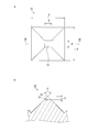
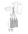
- FIG. 5 is a perspective plan view showing a schematic configuration of a general laminated lithium ion secondary battery 60.
- 61p is a positive electrode and 61n is a negative electrode.
- the positive and negative electrodes 61p and 61n each have a current collector made of metal foil as a base material layer.
- the substantially rectangular electrode portions 71p and 71n and the ear portions 62p protruding from one side of the electrode portions 71p and 71n. , 62n.
- an electrode mixture layer containing an active material is applied and formed on both surfaces of the current collector, while no electrode mixture layer is applied and formed on the ear portions 62p and 62n.
- the positive electrode 61p and the negative electrode 61n are alternately stacked via the separator 66 to constitute an electrode stacked body 67.
- the ears 62p of the plurality of positive electrodes 61p are overlapped with each other and welded by lead tabs 63p and welds 64p.
- the ears 62n of the plurality of negative electrodes 61n are overlapped with each other and welded by lead tabs 63n and welds 64n.
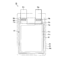
- 68 is an exterior housing the electrode laminate 67.
- the exterior 68 is composed of two laminate sheets (exterior materials) 69 having flexibility.
- the two laminate sheets 69 are heat-sealed and sealed by a heat seal part 69a along the outer peripheral edge.
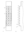
- FIG. 6 is a cross-sectional view along the thickness direction showing a schematic configuration of the negative electrode weld 64n and the vicinity thereof.
- 65p is a positive electrode current collector
- 66p is a positive electrode mixture layer applied to both surfaces of the positive electrode current collector 65p
- 65n is a negative electrode current collector
- 66n is applied to both surfaces of the negative electrode current collector 65n. Negative electrode mixture layer.
- a plurality of negative electrode current collectors 65n constituting the negative electrode ear portion 62n are superimposed on the negative electrode lead tab 63n, and these are integrally welded at the welding portion 64n.
- the configuration of the positive electrode weld 64p is substantially the same as that shown in FIG. 6 (see, for example, Patent Document 1).
- the positive electrode current collector 65p an aluminum foil with a thickness of about 15 ⁇ m is generally used, and as the positive electrode lead tab 63p, an aluminum thin plate with a thickness of about 200 ⁇ m is used.
- a copper foil having a thickness of about 10 ⁇ m is generally used as the negative electrode current collector 65n, and a nickel-plated copper thin plate having a thickness of about 200 ⁇ m is used as the negative electrode lead tab 63n.
- ultrasonic welding is used to weld the current collectors 65p and 65n constituting the ears 62p and 62n and the lead tabs 63p and 63n at the welds 64p and 64n.
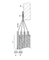
- FIG. 7 shows a case where the negative electrode weld 64n is formed, the positive electrode weld 64p is substantially the same.
- a plurality of negative electrode current collectors 65n constituting lead tabs 63n and ears 62n are sequentially stacked on the upper surface 51 of the anvil 50, and the chip 10 is placed on the negative electrode current collector 65n. While pressing the chip 10 against the negative electrode current collector 65n with the load F so as to compress the lead tab 63n and the negative electrode current collector 65n between the chip 10 and the anvil 50, the vibration is generated in a direction orthogonal to the direction of the load F.
- a sonic vibration S is applied to the chip 10.
- the ultrasonic vibration applied through the chip 10 heats the interfaces of the plurality of negative electrode current collectors 65n and the lead tabs 63n by frictional heat, thereby forming welds 64n (see FIGS. 5 and 6).
- the surface 51 (hereinafter referred to as “holding surface”) 51 that contacts the lead tab 63n of the anvil 50 is formed with fine irregularities of a predetermined shape.
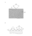
- FIG. 8A is a plan view showing an example of the shape of the processed surface 11 of the chip 10, and FIG. 8B is a front view thereof.
- a plurality of protrusions 15 having a quadrangular pyramid shape (a shape obtained by cutting off the top of the quadrangular pyramid along a plane parallel to the bottom surface) are formed on the processing surface 11 in vertical and horizontal directions. It is arranged in a grid in the direction.
- the shapes and dimensions of the plurality of protrusions 15 are the same.
- FIG. 9 is an enlarged plan view showing an example of a welded portion 64n formed by ultrasonic welding using the tip 10 having the processed surface 11 shown in FIGS. 8A and 8B.
- the processed surface 11 was in contact with the surface of the welded portion 64n shown in FIG.
- the uppermost negative electrode current collector 65n (hereinafter referred to as “the uppermost negative electrode current collector 65n”) has a protrusion 15 (FIGS. 8A and 8B) on the processed surface 11.
- the welding mark 25 which is a substantially quadrangular pyramid-shaped concave portion is formed by being pressed.
- the tear 30 is a tear generated in the uppermost negative electrode current collector 65n by ultrasonic welding.
- the tear 30 is likely to occur in the vicinity of the welding marks 25 arranged at the peripheral portion, particularly at the four corners, among the plurality of welding marks 25 arranged in a lattice shape.
- the ear portion 62n is thinner than the electrode portion because the mixture layer 66n is not formed. Since the plurality of negative electrode current collectors 65n constituting such thin ear portions 62n are bundled in the thickness direction between the chip 10 and the lead tab 63n, tension is easily applied to the negative electrode current collector 65n. .
- the uppermost negative electrode current collector 65n is locally extended along the shape of the protrusion 15. Therefore, in the uppermost negative electrode current collector 65n, it is considered that the tear 30 is likely to occur at a position in the vicinity of the welding mark 25 in the peripheral portion where the largest tension is easily applied among the plurality of welding marks 25.
- a rolled copper foil having relatively excellent elongation resistance is used as the copper foil constituting the negative electrode current collector 65n.
- this first method has a problem that the cost of the battery increases because the rolled copper foil is more expensive than the electrolytic copper foil.
- a copper dummy thin plate 80 having substantially the same thickness as the lead tab 63n is sandwiched between the chip 10 and the uppermost negative electrode current collector 65n.
- “dummy thin plate 80 / a plurality of negative electrode current collectors 65n / lead tabs 63n” are integrally ultrasonically welded. Since the processed surface 11 of the chip 10 is not pressed against the uppermost negative electrode current collector 65n, the weld mark 25 is hardly formed on the uppermost negative electrode current collector 65n. Therefore, the occurrence of the tear 30 can be suppressed.
- this second method has a problem that it is necessary to prepare the dummy thin plate 80, so that the cost is high, a problem that the ultrasonic welding work becomes complicated, and a problem that the welded portion 64n becomes thick. Yes.
- the current collector breakage may adversely affect the voltage characteristics of the finally obtained lithium ion secondary battery. Therefore, tearing reduces the manufacturing yield of the battery and also reduces the reliability of the battery.
- An object of the present invention is to provide a method of manufacturing a battery in which a current collector constituting an ear portion is hardly broken when the electrode ear portion and a lead tab are ultrasonically welded.
- a current collector is provided as a base material layer, and an electrode portion in which an electrode mixture layer is formed in a predetermined region of the current collector, and the electrode mixture layer is not formed.
- a plurality of electrodes each having an ear portion are stacked, and the plurality of ear portions and a lead tab having a thickness greater than that of the current collector are ultrasonically welded.
- the plurality of ears and the lead tab are disposed between a processing surface on which a plurality of protrusions of an ultrasonic welding tip are formed and a holding surface of the anvil, and the plurality of ears and While pressing the lead tab with the processing surface and the holding surface, ultrasonic vibration is applied from the processing surface to the plurality of ears and the lead tab.
- the ears farthest from the lead tab are in contact with the holding surface and the lead tabs are in contact with the processing surface. Place between.
- the lead tab comes into contact with the ultrasonic welding tip and the ear comes into contact with the anvil. Therefore, when ultrasonic welding is performed, the current collector constituting the ear is broken. The possibility can be reduced.
- FIG. 1 is a diagram showing a schematic configuration of an example of an ultrasonic welding machine used in the present invention.
- 2A is an enlarged plan view of the protrusion formed on the processed surface of the chip
- FIG. 2B is an enlarged cross-sectional view of the protrusion along the line 2B-2B in FIG. 2A.
- 3A is a plan view of the holding surface of the anvil
- FIG. 3B is an enlarged cross-sectional view of the protrusion formed on the holding surface of the anvil.
- FIG. 4 is a side view showing an ultrasonic welding process according to an embodiment of the present invention for forming a negative electrode weld.
- FIG. 5 is a perspective plan view showing a schematic configuration of a general laminated lithium ion secondary battery.
- FIG. 5 is a perspective plan view showing a schematic configuration of a general laminated lithium ion secondary battery.
- FIG. 6 is a cross-sectional view showing a schematic configuration of a welded portion between the ear portion of the negative electrode and the REIT tab and the vicinity thereof in the laminated lithium ion secondary battery shown in FIG.
- FIG. 7 is a side view showing a conventional ultrasonic welding process for forming the welded portion shown in FIG.
- FIG. 8A is a plan view showing an example of the shape of the processed surface of a conventional tip used in the ultrasonic welding process
- FIG. 8B is a front view thereof.
- FIG. 9 is an enlarged plan view showing an example of a welded portion formed by ultrasonic welding using the tip having the processed surface shown in FIGS. 8A and 8B.
- FIG. 10 is a side view showing a conventional ultrasonic welding process for preventing the current collector from being broken.
- the plurality of electrodes are electrodes for negative electrodes.
- the tear in the welding part of the copper foil generally used as a collector which comprises the electrode for negative electrodes can be reduced.
- the current collector is an electrolytic copper foil. Therefore, since the electrolytic copper foil is cheaper than the rolled copper foil, the cost of the battery can be reduced.
- the ultrasonic welder 1 includes a transmitter 2 that outputs an electrical signal having a predetermined frequency in the ultrasonic band, and a transducer that converts the electrical signal from the transmitter 2 into mechanical vibration in the ultrasonic band. 3, a booster 4 that converts the mechanical vibration generated by the vibrator 3 into ultrasonic vibration of a predetermined amplitude, a horn 5 that resonates by the ultrasonic vibration from the booster 4, and a super provided at one end of the horn 5.
- a sonic welding tip (hereinafter simply referred to as “tip”) 10 and an anvil 50 disposed to face the tip 10 are provided.
- the member to be welded is placed on the holding surface 51 of the anvil 50 and supported by the anvil 50.
- the processed surface 11 of the tip 10 is pressed against the member to be welded on the anvil 50, and a predetermined ultrasonic vibration is applied to the member to be welded through the tip 10.
- the configuration of the ultrasonic welding machine 1 used in the present invention is not limited to FIG.
- any known ultrasonic welding machine can be used.
- the chip 10 and the horn 5 may be constituted by one integrated part or may be constituted by separate parts.
- a plurality of protrusions protruding toward the anvil 50 are formed on the processed surface 11 of the chip 10.
- the arrangement of the plurality of protrusions and the shape of each protrusion are arbitrary.
- the processed surface 11 may be formed with a plurality of protrusions 15 having a quadrangular frustum shape shown in FIGS. 8A and 8B.
- 2A is an enlarged plan view of the protrusion 15
- FIG. 2B is an enlarged cross-sectional view of the protrusion 15 taken along the line 2B-2B of FIG. 2A.
- the protrusion 15 has a top portion 19 indicated by a two-dot chain line of a regular quadrangular pyramid having an angle (vertical angle) ⁇ of 90 ° formed by two opposing slopes parallel to the bottom surface of the quadrangular pyramid. It has a quadrangular frustum shape cut off along the surface.
- the bottom surface of the quadrangular pyramid is preferably a square having a side length A of 0.4 to 1.2 mm
- the top surface 16 is preferably a square having a side length B of 0.04 to 0.6 mm.
- the height C of the top 19 cut off is preferably 0.04 to 0.6 mm.
- the shape and size of the protrusion formed on the processed surface 11 are not limited thereto.
- the arrangement and the number of protrusions on the processed surface 11 are not limited to 16 in total in 2 rows ⁇ 8 columns in FIG. 8B.
- the plurality of protrusions formed on the processing surface 11 do not have to have the same shape and dimensions, and a plurality of kinds of protrusions having different shapes or dimensions may be mixed. Further, the protrusions do not have to be arranged in a lattice shape, and may be any arrangement such as a honeycomb shape.
- a plurality of protrusions protruding toward the chip 10 are also formed on the holding surface 51 of the anvil 50.
- 3A is a plan view of the holding surface 51 of the anvil 50
- FIG. 3B is an enlarged cross-sectional view of the protrusion 55 formed on the holding surface 51 of the anvil 50.
- a plurality of grooves 52 are formed in a lattice shape so as to be orthogonal to each other.
- each groove 52 has a V-shaped cross section with an internal angle of 90 °.
- a regular quadrangular pyramid-shaped protrusion 55 is formed between adjacent grooves 52.
- the height H of the protrusions 55 is preferably 0.2 to 0.5 mm, and the pitch P of the protrusions 55 is preferably 0.4 to 0.7 mm.
- the protrusion 55 illustrated in FIGS. 3A and 3B is merely an example, and the shape and dimensions of the protrusion formed on the holding surface 51 are not limited thereto. The arrangement and number of protrusions on the holding surface 51 are also arbitrary.
- the protrusion 15 formed on the processed surface 11 of the chip 10 is provided in order to efficiently transmit the ultrasonic vibration of the chip 10 to the member to be welded.
- the protrusion 55 formed on the holding surface 51 of the anvil 50 is provided to hold the member to be welded on the holding surface 51 so that the member to be welded does not move with the tip 10.
- the height and pitch of the protrusions 15 formed on the processed surface 11 are set larger than those of the protrusions 55 formed on the holding surface 51.
- FIG. 4 is a side view showing an ultrasonic welding process according to an embodiment of the present invention for forming the negative electrode weld 64n.
- the arrangement of the lead tab 63n as a member to be welded and the plurality of negative electrode current collectors 65n is reversed from FIG. ing. That is, in the present invention, a plurality of negative electrode current collectors 65n and lead tabs 63n are placed in this order on the holding surface 51 of the anvil 50, and the processed surface 11 of the chip 10 is pressed against the lead tabs 63n with a load F. In this state, an ultrasonic vibration S that vibrates in a direction orthogonal to the direction of the load F is applied to the chip 10 to ultrasonically weld the plurality of negative electrode current collectors 65n and the lead tabs 63n to each other.
- the protrusion 15 formed on the processed surface 11 of the chip 10 is not directly pressed against the negative electrode current collector 65n, the negative electrode current collector 65n is welded by the protrusion 15 as shown in FIG. The mark 25 is not formed, and the tear 30 does not occur.
- the lowermost negative electrode current collector 65n (hereinafter referred to as the “lowermost negative electrode current collector 65n”) with which the holding surface 51 of the anvil 50 abuts among the plurality of current collectors 65n, There may be a case where a welding mark (concave portion) is formed by pressing the protrusion 55 formed on the holding surface 51.
- a welding mark concave portion
- the inventor has confirmed through experiments that it is relatively easy to set ultrasonic welding conditions so that the lowermost negative electrode current collector 65n is not broken.
- the negative electrode current collector 65n is connected to the negative electrode current collector 65n during ultrasonic welding.
- tension is applied, in FIG. 7, the stress tends to concentrate in the vicinity of the portion where the protrusion 15 of the uppermost negative electrode current collector 65n contacts.
- the protrusion 15 of the chip 10 that is ultrasonically vibrated is directly pressed against the uppermost negative electrode current collector 65n, the protrusion 15 of the uppermost negative electrode current collector 65n is extremely pressed.
- the protrusion 15 on the processed surface 11 of the chip 10 is in contact with the lead tab 63n.
- the lead tab 63n is thicker than the negative electrode current collector 65n, the lead tab 63n may be broken. There is almost no.
- the negative electrode current collector 65n and the lead tab 63n constituting the ear portion 62n are ultrasonically welded to form the welded portion 64n, the negative electrode current collector 65n is broken. The possibility of doing so can be reduced. Therefore, the yield is improved and a highly reliable battery can be provided.
- the negative electrode current collector since the occurrence of breakage of the negative electrode current collector can be reduced, a relatively inexpensive electrolytic copper foil can be used as the negative electrode current collector, so that the cost of the battery can be reduced. Further, it is not necessary to use the dummy thin plate 80 shown in FIG.
- the breakage of the negative electrode current collector 65n can be reduced by an extremely simple method in which the lead tab 63n is arranged on the anvil 50 side and the negative electrode current collector 65n is arranged on the chip 10 side.
- the ultrasonic welding apparatus 1 including the tip 10 and the anvil 50 can be used as it is without any change, so that the cost effectiveness is extremely high.
- the negative electrode weld 64n is formed has been described.
- the positive electrode weld 64p can also be formed by the same method, and in this case, the same effect as described above can be obtained.
- Embodiment 2 The ultrasonic welding process of the present invention described in Embodiment 1 can be used for welding the electrode tabs and lead tabs of a battery (particularly, the laminated lithium ion secondary battery 60 shown in FIG. 5).
- the general configuration of the lithium ion secondary battery 60 will be outlined below.
- the positive electrode 61p has, for example, a structure in which a layer (positive electrode mixture layer) 66p made of a positive electrode mixture containing a positive electrode active material, a conductive additive, a binder, and the like is formed on one or both surfaces of the current collector 65p.
- a layer (positive electrode mixture layer) 66p made of a positive electrode mixture containing a positive electrode active material, a conductive additive, a binder, and the like is formed on one or both surfaces of the current collector 65p.
- a positive electrode active material consists of an active material which can occlude / release lithium ion.
- Such a positive electrode active material includes, for example, lithium having a layered structure represented by Li 1 + x MO 2 ( ⁇ 0.1 ⁇ x ⁇ 0.1, M: Co, Ni, Mn, Al, Mg, etc.) Transition metal oxide, LiMn 2 O 4 , lithium manganese oxide having a spinel structure in which part of the element is replaced with another element, and olivine type represented by LiMPO 4 (M: Co, Ni, Mn, Fe, etc.) It preferably consists of any one of compounds.
- Lithium-containing transition metal oxide of the above layered structure for example, LiCoO 2, LiNi 1-x Co xy Al y O 2 (0.1 ⁇ x ⁇ 0.3,0.01 ⁇ y ⁇ 0.2), And an oxide containing at least Co, Ni and Mn (LiMn 1/3 Ni 1/3 Co 1/3 O 2 , LiMn 5/12 Ni 5/12 Co 1/6 O 2 , LiNi 3/5 Mn 1/5 Co 1/5 O 2 or LiNi 0.5 Co 0.2 Mn 0.3 ) is preferable.
- the current collector 65p of the positive electrode 61p is preferably made of, for example, an aluminum foil or an aluminum alloy foil.
- the thickness of the current collector 65p varies depending on the size and capacity of the battery, but is preferably 0.01 to 0.02 mm, for example.
- the positive electrode 61p is manufactured by the following method.
- a positive electrode mixture containing the above-described positive electrode active material, a conductive additive such as graphite, acetylene black, carbon black, and fibrous carbon, and a binder such as polyvinylidene fluoride (PVDF) is used as N-methyl-2-pyrrolidone.
- a paste-like or slurry-like composition uniformly dispersed using a solvent such as (NMP) is prepared (the binder may be dissolved in the solvent). This composition is intermittently applied onto a strip-shaped current collector and dried. You may adjust the thickness of a positive mix layer by press processing as needed.
- the long positive electrode substrate (electrode substrate) thus obtained is cut into a predetermined shape using, for example, a Thomson blade to obtain the positive electrode 61p.
- the thickness of the positive electrode mixture layer 66p in the positive electrode 61p is preferably 30 to 100 ⁇ m per side.
- the content of each component in the positive electrode mixture layer 66p is preferably positive electrode active material: 90 to 98% by mass, conductive auxiliary agent: 1 to 5% by mass, and binder: 1 to 5% by mass.
- the positive electrode lead tab 63p is preferably made of aluminum or an aluminum alloy.
- the thickness of the positive electrode lead tab 63p is preferably 20 to 300 ⁇ m.
- the positive electrode lead tab 63 p is led out to the outside of the outer package 68, but a positive electrode terminal of another member is connected to the positive electrode lead tab 63 p and the positive electrode terminal is led out of the outer package 68. Also good.
- the material of such a positive electrode terminal is determined from the viewpoint of facilitating connection with a device that uses the battery 60. For example, aluminum or an aluminum alloy can be used.
- the thickness of the positive electrode terminal is preferably 50 to 300 ⁇ m.
- the ultrasonic welding method of the present invention described in the first embodiment can be used.
- various methods such as resistance welding, laser welding, caulking, and adhesion using a conductive adhesive can also be used.
- the negative electrode 61n has, for example, a structure in which a layer (negative electrode mixture layer) 66n containing a negative electrode active material capable of occluding and releasing lithium ions is formed on one surface or both surfaces of the current collector 65n.
- Negative electrode active materials include graphite, pyrolytic carbons, cokes, glassy carbons, fired organic polymer compounds, mesocarbon microbeads (MCMB), and carbon that can occlude and release lithium ions such as carbon fibers. It is preferable that it consists of 1 type, or 2 or more types of mixtures of system material.
- the negative electrode active material may be an element such as Si, Sn, Ge, Bi, Sb, or In, an alloy of Si, Sn, Ge, Bi, Sb, or In, a lithium-containing nitride, or a lithium metal such as lithium oxide. It is preferably made of any of a compound (LiTi 3 O 12 or the like) that can be charged and discharged at a near low voltage, lithium metal, and a lithium / aluminum alloy.
- a copper foil is suitable as the current collector 65n of the negative electrode 61n. Copper foils are roughly classified into electrolytic copper foils and rolled copper foils depending on the manufacturing method. Electrolytic copper foil is relatively inexpensive. The thickness of the current collector 65n varies depending on the size or capacity of the battery, but is preferably 0.005 to 0.02 mm, for example.
- the negative electrode 61n is manufactured by the following method.
- the negative electrode active material described above a binder (such as a mixed binder of rubber binder such as PVDF or styrene butadiene rubber (SBR) and carboxymethyl cellulose (CMC)), and graphite, acetylene black, carbon black, etc.
- a paste-like or slurry-like composition in which a negative electrode mixture containing a conductive aid or the like is uniformly dispersed using a solvent such as NMP or water is prepared (the binder may be dissolved in the solvent). .
- This composition is intermittently applied onto a strip-shaped current collector and dried. You may adjust the thickness or density of a negative mix layer by press processing as needed.
- the long negative electrode substrate (electrode substrate) thus obtained is cut into a predetermined shape using, for example, a Thomson blade to obtain a negative electrode 61n.
- the thickness of the negative electrode mixture layer 66n in the negative electrode 61n is preferably 30 to 100 ⁇ m per side.
- the content of each component in the negative electrode mixture layer 66n is preferably 90 to 98% by mass of the negative electrode active material and 1 to 5% by mass of the binder.
- the content of the conductive auxiliary in the negative electrode mixture layer 66n is preferably 1 to 5% by mass.
- the negative electrode lead tab 63n is preferably made of copper. If necessary, nickel plating or the like may be applied to the surface.
- the thickness of the negative electrode lead tab 63n is preferably 20 to 300 ⁇ m.
- the negative electrode lead tab 63 n is led out to the outside of the outer package 68, but a negative electrode terminal of another member is connected to the negative electrode lead tab 63 n and the negative electrode terminal is led out of the outer package 68. Also good.
- the material of such a negative electrode terminal is determined from the viewpoint of facilitating connection with a device that uses the battery 60. For example, nickel, nickel-plated copper, nickel-copper clad, and the like can be used. Further, the thickness of the negative electrode terminal is preferably 50 to 300 ⁇ m, similarly to the positive electrode terminal.
- the ultrasonic welding method of the present invention described in the first embodiment can be used.
- the ultrasonic welding method of the present invention can reduce the occurrence of tearing of the metal foil, even when using an electrolytic copper foil having relatively poor elongation resistance as the negative electrode current collector 65n, A battery in which the ear 62n made of the negative electrode current collector 65n is not broken can be manufactured. As a result, the cost of the battery can be reduced by using a relatively inexpensive electrolytic copper foil.
- various methods such as resistance welding, laser welding, caulking, adhesion with a conductive adhesive, and the like can be used as a method for connecting the ear 62n and the negative electrode lead tab 63n.
- the separator 66 includes a porous film that separates the positive electrode 61p and the negative electrode 61n and transmits lithium ions.
- the separator 66 preferably has a safety mechanism (shutdown characteristic) that melts and closes the hole when the battery 60 abnormally generates heat and reaches a high temperature (for example, 100 to 140 ° C.).
- the porous film is preferably made of a thermoplastic resin having a melting point of about 80 to 140 ° C., and specifically, preferably made of a polyolefin polymer such as polypropylene or polyethylene.
- the thickness of the porous film is not particularly limited, but is preferably 10 to 50 ⁇ m.
- the separator 66 may be formed by coating a plate-like inorganic fine particle layer on the porous film. Thereby, the thermal contraction of the separator 66 at the time of abnormal heat generation can be suppressed, and safety can be improved.
- the separator 66 may have a laminated structure of the porous film and the heat-resistant porous substrate.
- a fibrous material having a heat resistant temperature of 150 ° C. or higher can be used as the heat resistant porous substrate.
- the fibrous material may be formed of at least one material selected from the group consisting of cellulose and its modified products, polyolefin, polyethylene terephthalate, polybutylene terephthalate, polypropylene, polyester, polyacrylonitrile, aramid, polyamideimide, and polyimide. it can. Specifically, it is preferably made of a nonwoven fabric made of the above materials.
- Heat resistance of a porous substrate means that substantial dimensional change due to softening or the like does not occur. Specifically, is the upper limit temperature (heat resistant temperature) at which the rate of shrinkage (shrinkage ratio) with respect to the length of the porous substrate at room temperature maintained at 5% or less is sufficiently higher than the shutdown temperature of the separator? The heat resistance is evaluated based on the result. In order to increase the safety of the laminated battery after shutdown, it is desirable that the porous substrate has a heat resistance higher by 20 ° C. than the shutdown temperature. More specifically, the heat resistance temperature of the porous substrate is 150 ° C. It is preferable that the temperature is higher than or equal to ° C, and more preferable that the temperature is higher than or equal to 180 ° C.
- a solution (nonaqueous electrolytic solution) in which a solute such as LiPF 6 or LiBF 4 is dissolved in a high dielectric constant solvent or an organic solvent can be used.
- a solute such as LiPF 6 or LiBF 4
- a high dielectric constant solvent any of ethylene carbonate (EC), propylene carbonate (PC), and ⁇ -butyrolactone (BL) can be used.
- a low viscosity solvent such as linear dimethyl carbonate (DMC), diethyl carbonate (DEC), or methyl ethyl carbonate (EMC) can be used.
- the solvent for the electrolytic solution it is preferable to use a mixed solvent of the above-described high dielectric constant solvent and low viscosity solvent.
- PVDF a rubber-based material, an alicyclic epoxy, a material having an oxetane-based three-dimensional crosslinked structure, and the like may be mixed and solidified into the above-described solution to form a polymer electrolyte.
- the separator 66 is interposed between the positive electrode 61p and the negative electrode 61n, and the positive electrode 61p and the negative electrode 61n are alternately stacked to form an electrode laminate 67.
- the method for producing the electrode laminate 67 is not particularly limited.
- the band-shaped separator 66 is alternately zigzag-folded by alternately repeating mountain folds and valley folds at regular intervals, and the positive electrode 61p is sandwiched between the one surface side of the separator 66 and each valley fold portion, and the other surface side
- the electrode laminate 67 can be formed by sandwiching the negative electrode 61n in each valley folded portion.
- the electrode stack 67 may be formed by forming a plurality of rectangular bags with the separators 66 and inserting the positive electrodes 61p into the bags made of the separators 66 alternately with the negative electrodes 61n. .
- the positive electrode lead tab 63p is connected to the positive electrode ear portion 62p of the plurality of positive electrode electrodes 61p protruding from the electrode laminate 67 thus obtained.
- the negative electrode lead tab 63n is connected to the negative electrode ears 62n of the plurality of negative electrodes 61n protruding from the electrode laminate 67.
- Two laminate sheets 69 having a substantially rectangular shape are arranged above and below the electrode laminate 67 thus obtained, and two laminate sheets are disposed along three sides excluding the side where the positive electrode lead tab 63p and the negative electrode lead tab 63n are formed.
- 69 is heat-sealed to form a laminate sheet 69 into a bag shape.
- one rectangular laminate sheet is folded and stacked so as to sandwich the electrode laminate 67, and heat-sealed along two opposing sides to form a laminate sheet in a bag shape It may be formed.
- an electrolytic solution is injected into the bag of the laminate sheet 69.
- the laminate sheet 69 is heat-sealed together with the positive and negative lead tabs 63p and 63n along the side that is not heat-sealed, whereby the lithium ion secondary battery 60 is obtained.
- the configuration of the laminate sheet 69 is not particularly limited, and for example, a known laminate sheet used as an exterior material of a laminated lithium ion secondary battery can be used.
- a multilayer sheet in which a modified polyolefin layer is laminated as a heat-fusible resin layer on one side of a base layer made of aluminum can be used.
- the positive electrode lead tab 63p and the negative electrode lead tab 63n are drawn from the same short side of the substantially rectangular laminate sheet 69, but may be drawn from different sides.
- the chip 10 of the present invention can also be used for manufacturing a lithium ion secondary battery other than the laminated type.
- An electrode laminate 67 (see FIG. 5) for the laminated lithium ion secondary battery 60 was prepared as follows.
- the positive electrode current collector 65p an aluminum foil having a thickness of 15 ⁇ m was used.
- the negative electrode current collector 65n an electrolytic copper foil having a thickness of 10 ⁇ m was used.
- a negative electrode mixture layer 66n having a thickness of 126 ⁇ m was applied and formed in a predetermined region on both surfaces of the current collector 65n to obtain a negative electrode 61n.
- a strip-shaped separator 66 made of a porous film and having a thickness of 21 ⁇ m is folded in a zigzag shape, and the positive electrode 61p is sandwiched from one side of the separator 66 to each valley fold, and the above-mentioned each valley fold from the other side.
- the negative electrode 61n was sandwiched to obtain an electrode laminate 67 in which 19 positive electrodes 61p and 20 negative electrodes 61n were alternately stacked with separators 66 interposed therebetween.
- the tabs 62n of the 20 negative electrodes 61n protruding from one side of the electrode laminate 67 and the lead tabs 63n (20 mm width Cu—Ni) having a thickness of 200 ⁇ m and a width of 20 mm were joined by ultrasonic welding.
- the lead tab 63n is obtained by performing nickel plating on both surfaces of a copper thin plate.
- 16 projections 15 having a truncated pyramid shape were arranged in a grid in 2 rows ⁇ 8 columns. . 2A and 2B, the bottom surface of the protrusion 15 is a square having a side length A of 1.2 mm, and the upper surface 16 is a square having a side length B of 0.96 mm. The height C of the top portion 19 from which the protrusions 15 were cut off was 0.48 mm.
- a plurality of projections 55 having a regular quadrangular pyramid shape are formed on the holding surface 51 of the anvil 50 used for ultrasonic welding by a plurality of grooves 52 formed in a lattice shape. It had been.
- the height H of the protrusions 55 was 0.25 mm, and the pitch P of the protrusions 55 was 0.5 mm.
- ultrasonic welding was performed under a plurality of types of ultrasonic welding conditions in which the load F applied to the chip 10, the amplitude of the ultrasonic vibration S, the welding time, and the like were different.
- the welded portion 64n was observed with a digital microscope, and the presence or absence of breakage of the current collector 65n constituting the ear portion 62n and the presence or absence of poor welding at the welded portion 64n were examined.
- the battery manufacturing method of the present invention can be preferably used for manufacturing a secondary battery in which sheet-like positive electrodes and sheet-like negative electrodes are alternately arranged via separators.
Landscapes
- Chemical & Material Sciences (AREA)
- Chemical Kinetics & Catalysis (AREA)
- Electrochemistry (AREA)
- General Chemical & Material Sciences (AREA)
- Engineering & Computer Science (AREA)
- Manufacturing & Machinery (AREA)
- Materials Engineering (AREA)
- Connection Of Batteries Or Terminals (AREA)
Abstract
Selon la présente invention, un soudage par ultrasons est effectué avec une pluralité de sections d'oreille (62n) et une languette avant (63n) disposées entre une enclume (50) et une pointe (10) de manière à ce que les sections d'oreille (62n) entrent en contact avec la surface usinée (51) de l'enclume (50), et la languette avant (63n) entre en contact avec la surface usinée (11) de la pointe (10) du soudage par ultrasons. En conséquence de quoi, il est possible de réduire le phénomène de rupture d'un collecteur qui configure les sections d'oreille (62n).
Applications Claiming Priority (2)
| Application Number | Priority Date | Filing Date | Title |
|---|---|---|---|
| JP2012-004303 | 2012-01-12 | ||
| JP2012004303 | 2012-01-12 |
Publications (1)
| Publication Number | Publication Date |
|---|---|
| WO2013105362A1 true WO2013105362A1 (fr) | 2013-07-18 |
Family
ID=48781324
Family Applications (1)
| Application Number | Title | Priority Date | Filing Date |
|---|---|---|---|
| PCT/JP2012/081284 WO2013105362A1 (fr) | 2012-01-12 | 2012-12-03 | Procédé permettant de produire une batterie |
Country Status (1)
| Country | Link |
|---|---|
| WO (1) | WO2013105362A1 (fr) |
Cited By (6)
| Publication number | Priority date | Publication date | Assignee | Title |
|---|---|---|---|---|
| WO2018159197A1 (fr) * | 2017-02-28 | 2018-09-07 | 日立オートモティブシステムズ株式会社 | Accumulateur |
| EP3316349A4 (fr) * | 2015-06-25 | 2018-12-26 | NEC Energy Devices, Inc. | Procédé de fabrication de dispositif électrochimique |
| JP2021018845A (ja) * | 2019-07-17 | 2021-02-15 | 古河電池株式会社 | 非水電解質二次電池およびその製造方法 |
| CN113097656A (zh) * | 2021-05-10 | 2021-07-09 | 厦门海辰新能源科技有限公司 | 极片、电芯组件和电池 |
| US20220241890A1 (en) * | 2019-07-31 | 2022-08-04 | Vehicle Energy Japan Inc. | Ultrasonic horn, secondary battery, and method for manufacturing secondary battery |
| WO2024062522A1 (fr) * | 2022-09-20 | 2024-03-28 | 株式会社 東芝 | Batterie secondaire et procédé de fabrication d'une batterie secondaire |
Citations (3)
| Publication number | Priority date | Publication date | Assignee | Title |
|---|---|---|---|---|
| JP2008000638A (ja) * | 2006-06-20 | 2008-01-10 | Nec Tokin Corp | 超音波ホーン |
| JP2011071109A (ja) * | 2009-08-27 | 2011-04-07 | Toshiba Corp | 電池 |
| JP2011204552A (ja) * | 2010-03-26 | 2011-10-13 | Mitsubishi Heavy Ind Ltd | 電池、及びこの電池の製造に用いられる超音波溶接システム |
-
2012
- 2012-12-03 WO PCT/JP2012/081284 patent/WO2013105362A1/fr active Application Filing
Patent Citations (3)
| Publication number | Priority date | Publication date | Assignee | Title |
|---|---|---|---|---|
| JP2008000638A (ja) * | 2006-06-20 | 2008-01-10 | Nec Tokin Corp | 超音波ホーン |
| JP2011071109A (ja) * | 2009-08-27 | 2011-04-07 | Toshiba Corp | 電池 |
| JP2011204552A (ja) * | 2010-03-26 | 2011-10-13 | Mitsubishi Heavy Ind Ltd | 電池、及びこの電池の製造に用いられる超音波溶接システム |
Cited By (9)
| Publication number | Priority date | Publication date | Assignee | Title |
|---|---|---|---|---|
| EP3316349A4 (fr) * | 2015-06-25 | 2018-12-26 | NEC Energy Devices, Inc. | Procédé de fabrication de dispositif électrochimique |
| WO2018159197A1 (fr) * | 2017-02-28 | 2018-09-07 | 日立オートモティブシステムズ株式会社 | Accumulateur |
| JPWO2018159197A1 (ja) * | 2017-02-28 | 2019-06-27 | 日立オートモティブシステムズ株式会社 | 二次電池 |
| JP2021018845A (ja) * | 2019-07-17 | 2021-02-15 | 古河電池株式会社 | 非水電解質二次電池およびその製造方法 |
| JP7336287B2 (ja) | 2019-07-17 | 2023-08-31 | 古河電池株式会社 | 非水電解質二次電池およびその製造方法 |
| US20220241890A1 (en) * | 2019-07-31 | 2022-08-04 | Vehicle Energy Japan Inc. | Ultrasonic horn, secondary battery, and method for manufacturing secondary battery |
| CN113097656A (zh) * | 2021-05-10 | 2021-07-09 | 厦门海辰新能源科技有限公司 | 极片、电芯组件和电池 |
| CN113097656B (zh) * | 2021-05-10 | 2023-04-25 | 厦门海辰储能科技股份有限公司 | 极片、电芯组件和电池 |
| WO2024062522A1 (fr) * | 2022-09-20 | 2024-03-28 | 株式会社 東芝 | Batterie secondaire et procédé de fabrication d'une batterie secondaire |
Similar Documents
| Publication | Publication Date | Title |
|---|---|---|
| WO2013105361A1 (fr) | Bec de soudage par ultrasons, machine de soudage par ultrasons et procédé de production de batterie | |
| JP5768137B2 (ja) | シート状電極の製造方法 | |
| JP5830953B2 (ja) | 二次電池、バッテリユニットおよびバッテリモジュール | |
| JP5701688B2 (ja) | 積層式電池およびその製造方法 | |
| US20120244423A1 (en) | Laminate case secondary battery | |
| JP6504158B2 (ja) | 積層型電池及びその製造方法 | |
| US20110244304A1 (en) | Stack type battery | |
| JP2015199095A (ja) | 超音波溶接装置、及び電池の製造方法 | |
| WO2015129320A1 (fr) | Électrode pour cellule secondaire, cellule secondaire et procédé de fabrication d'électrode pour cellule secondaire et de cellule secondaire | |
| JP2009176513A (ja) | 非水電解質電池および非水電解質電池の製造方法 | |
| WO2013105362A1 (fr) | Procédé permettant de produire une batterie | |
| KR20120053463A (ko) | 비-수성 전해질 전지 | |
| WO2011002064A1 (fr) | Batterie stratifiée | |
| CN107851768B (zh) | 电化学器件的制造方法 | |
| JP2012221804A (ja) | 組電池 | |
| WO2014141640A1 (fr) | Cellule extérieure de stratifié | |
| JP2012151036A (ja) | ラミネート形電池 | |
| JP5161421B2 (ja) | 非水電解質電池 | |
| JP2013165054A (ja) | 電池 | |
| WO2017098995A1 (fr) | Dispositif électrochimique et procédé de sa fabrication | |
| JP2017107719A (ja) | 角形二次電池 | |
| JP2012164476A (ja) | ラミネート形電池およびそれを備えた積層型電池 | |
| JP2009110812A (ja) | 電池及びその製造方法 | |
| JP6781074B2 (ja) | 二次電池 | |
| JP2011216209A (ja) | ラミネート形電池およびその製造方法 |
Legal Events
| Date | Code | Title | Description |
|---|---|---|---|
| 121 | Ep: the epo has been informed by wipo that ep was designated in this application |
Ref document number: 12864891 Country of ref document: EP Kind code of ref document: A1 |
|
| NENP | Non-entry into the national phase |
Ref country code: DE |
|
| 122 | Ep: pct application non-entry in european phase |
Ref document number: 12864891 Country of ref document: EP Kind code of ref document: A1 |
|
| NENP | Non-entry into the national phase |
Ref country code: JP |