WO2013103045A1 - スクライブ方法 - Google Patents
スクライブ方法 Download PDFInfo
- Publication number
- WO2013103045A1 WO2013103045A1 PCT/JP2012/078668 JP2012078668W WO2013103045A1 WO 2013103045 A1 WO2013103045 A1 WO 2013103045A1 JP 2012078668 W JP2012078668 W JP 2012078668W WO 2013103045 A1 WO2013103045 A1 WO 2013103045A1
- Authority
- WO
- WIPO (PCT)
- Prior art keywords
- scribing
- cutting edge
- groove
- scribe
- substrate
- Prior art date
- Legal status (The legal status is an assumption and is not a legal conclusion. Google has not performed a legal analysis and makes no representation as to the accuracy of the status listed.)
- Ceased
Links
Images



Classifications
-
- H—ELECTRICITY
- H10—SEMICONDUCTOR DEVICES; ELECTRIC SOLID-STATE DEVICES NOT OTHERWISE PROVIDED FOR
- H10F—INORGANIC SEMICONDUCTOR DEVICES SENSITIVE TO INFRARED RADIATION, LIGHT, ELECTROMAGNETIC RADIATION OF SHORTER WAVELENGTH OR CORPUSCULAR RADIATION
- H10F19/00—Integrated devices, or assemblies of multiple devices, comprising at least one photovoltaic cell covered by group H10F10/00, e.g. photovoltaic modules
- H10F19/30—Integrated devices, or assemblies of multiple devices, comprising at least one photovoltaic cell covered by group H10F10/00, e.g. photovoltaic modules comprising thin-film photovoltaic cells
- H10F19/31—Integrated devices, or assemblies of multiple devices, comprising at least one photovoltaic cell covered by group H10F10/00, e.g. photovoltaic modules comprising thin-film photovoltaic cells having multiple laterally adjacent thin-film photovoltaic cells deposited on the same substrate
- H10F19/33—Patterning processes to connect the photovoltaic cells, e.g. laser cutting of conductive or active layers
-
- Y—GENERAL TAGGING OF NEW TECHNOLOGICAL DEVELOPMENTS; GENERAL TAGGING OF CROSS-SECTIONAL TECHNOLOGIES SPANNING OVER SEVERAL SECTIONS OF THE IPC; TECHNICAL SUBJECTS COVERED BY FORMER USPC CROSS-REFERENCE ART COLLECTIONS [XRACs] AND DIGESTS
- Y02—TECHNOLOGIES OR APPLICATIONS FOR MITIGATION OR ADAPTATION AGAINST CLIMATE CHANGE
- Y02E—REDUCTION OF GREENHOUSE GAS [GHG] EMISSIONS, RELATED TO ENERGY GENERATION, TRANSMISSION OR DISTRIBUTION
- Y02E10/00—Energy generation through renewable energy sources
- Y02E10/50—Photovoltaic [PV] energy
- Y02E10/541—CuInSe2 material PV cells
-
- Y—GENERAL TAGGING OF NEW TECHNOLOGICAL DEVELOPMENTS; GENERAL TAGGING OF CROSS-SECTIONAL TECHNOLOGIES SPANNING OVER SEVERAL SECTIONS OF THE IPC; TECHNICAL SUBJECTS COVERED BY FORMER USPC CROSS-REFERENCE ART COLLECTIONS [XRACs] AND DIGESTS
- Y02—TECHNOLOGIES OR APPLICATIONS FOR MITIGATION OR ADAPTATION AGAINST CLIMATE CHANGE
- Y02P—CLIMATE CHANGE MITIGATION TECHNOLOGIES IN THE PRODUCTION OR PROCESSING OF GOODS
- Y02P70/00—Climate change mitigation technologies in the production process for final industrial or consumer products
- Y02P70/50—Manufacturing or production processes characterised by the final manufactured product
Definitions
- the present invention relates to a scribing method used for manufacturing a solar cell submodule, and more particularly, to a scribing method capable of performing stable scribing for a long period of time and extending the life of a blade used.
- a solar cell is configured by a large number of solar cells having a laminated structure in which a semiconductor photoelectric conversion layer that generates a current by light absorption is sandwiched between a back electrode and a transparent electrode, which are connected in series on an insulating substrate.
- solar cells those using chalcopyrite-based CuInSe 2 (CIS) or Cu (In, Ga) Se 2 (hereinafter also simply referred to as CIGS) for the photoelectric conversion layer have been studied.
- CIS chalcopyrite-based CuInSe 2
- Cu (In, Ga) Se 2 hereinafter also simply referred to as CIGS
- a solar cell using a CIGS film as a photoelectric conversion layer has been studied actively because it has a relatively high efficiency and has a high light absorption rate, so that it can be made thin.
- a conventional solar cell having a configuration shown in FIG. 9A is known, and an integrated structure is obtained through an integration process described below.
- the back electrode 112 made of Mo layers separated from each other is formed on the surface of the insulating substrate 110, for example, by forming a first separation groove P ⁇ b> 1.
- a photoelectric conversion layer 114 made of a CIGS layer is formed so as to cover the first separation groove P1 and the back electrode 112.
- a buffer layer 116 made of a CdS layer is formed on the photoelectric conversion layer 114.
- a second separation groove P2 reaching the back electrode 112 from the buffer layer 116 is formed by mechanical scribing at a position different from the first separation groove P1.
- the photoelectric conversion layer 114 and the buffer layer 116 are divided by the second separation groove P2.
- a transparent electrode 118 made of AZO (Al 2 O 3 : ZnO) is formed so as to cover the buffer layer 116 and fill the second separation groove P2.
- a third separation groove P3 reaching the back electrode 112 from the transparent electrode 118 is formed at a position different from the first separation groove P1 and the second separation groove P2, for example, by mechanical scribing.
- the back surface electrode 112, the photoelectric conversion layer 114, the buffer layer 116, and the transparent electrode 118 separated by the third separation groove P3 constitute a solar battery cell 120.
- the solar battery cell 120 is formed to extend in the width direction W of the insulating substrate 110.
- the solar battery cell 120 is connected in series with the solar battery cell 120 adjacent in the longitudinal direction L of the edge substrate 110.
- the first separation groove P1, the second separation groove P2, and the third separation groove P3 are fine grooves each having a width of about 30 to 60 ⁇ m.
- a mechanical scribe device is used to form a fine groove of about 30 to 60 ⁇ m.
- FIG. 10A when the workpiece B is scribed using a case where the cutting edge 130 is new, that is, in the case of a new blade, as shown in FIG. A normal scribe region 140 is obtained, and a predetermined scribe groove is formed.
- edge part 134 of the cutting edge is used when a new blade is used, the following problems occur.
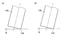
- the edge portion 134 of the new blade has significant initial wear, and a chamfered portion 132 is formed as shown in FIG. 10 (b), resulting in a decrease in surface pressure due to an increase in contact area.
- slip occurs and a scribe groove formation failure occurs.
- load control maintenance is required, which affects the operation of the scribe.
- a scribing apparatus shown in Patent Document 1 has been proposed.
- the tip of the cylindrical body is tapered with a predetermined taper angle, and the blade with the tapered tip flattened is pressed vertically against the scribe portion of the work surface with a predetermined pressure.
- Means for scribing by moving along the work surface means for measuring the size of the flat part of the blade tip, and controlling the pressing force of the blade according to the measured size of the flat part
- a mechanical scribing device constituted by the above-mentioned means.
- the means for measuring the size of the flat portion at the tip of the blade includes a camera unit, and the size of the flat portion at the tip of the blade is measured by the camera unit.
- An object of the present invention is to provide a scribing method that eliminates the problems based on the above-described conventional technology and enables stable scribing over a long period of time.
- the present invention forms a groove in a workpiece by pressing the cutting edge against the workpiece at a specified angle and moving the cutting edge in a predetermined scribe direction while maintaining the specified angle.
- a scribing method including a scribing step, wherein the tip portion of the blade edge is aged or chamfered by chamfering.
- a notch forming process that forms a notch at the groove forming start position of the workpiece using the cutting edge, and after the cutting is formed, the cutting edge is separated from the workpiece, and then the scribing process It is preferable to shift to. Moreover, it is preferable that a notch formation process inclines in the scribing direction side rather than the angle of the blade edge in a scribing process, and forms a notch in a groove
- the chamfering amount at the tip of the blade edge is 5 ⁇ m to 50 ⁇ m.
- the angle of the blade edge in the scribing step is 60 ° or more and less than 90 °.
- the angle at which the blade edge is inclined toward the scribe direction in the notch forming step is 5 ° to 10 °.
- the tip of the cutting edge is chamfered in advance by aging or chamfering, so that stable scribing can be achieved for a long period of time. Further, slip generated by the initial wear is suppressed, and the quality of the groove is deteriorated, and the condition setting change and operation loss associated therewith can be reduced. Furthermore, a groove can be formed with a low load by forming a cut at the groove formation start position. As a result, it is possible to suppress the wear of the blade edge and damage such as chipping of the blade edge, thereby extending the life of the blade edge.
- FIG. 1 It is typical sectional drawing which shows an example of the solar cell module formed using the scribing method of embodiment of this invention.
- FIG. 1 (A)-(g) is typical sectional drawing which shows the manufacturing method of the solar cell module formed using the scribing method of embodiment of this invention in order of a process.
- (A), (b) is a schematic diagram which shows an example of the scribing method of embodiment of this invention, respectively.
- (A) is a graph which shows the relationship between the amount of initial wear of a blade edge
- (b) is a graph which shows the relationship between a blade edge
- (c) is a blade edge load, and a scribe. It is a graph which shows the relationship with distance.
- FIG. 1 It is a schematic diagram for demonstrating the abrasion amount of a blade edge
- (A), (b) is a schematic plan view which shows the scribing method of embodiment of this invention in process order.
- (A), (b) is a schematic diagram which shows the other example of the scribing method of embodiment of this invention, respectively.
- (A) is typical sectional drawing which shows the conventional solar cell,
- (b) is a typical top view which shows the conventional solar cell.
- (A), (b) is a schematic diagram which shows the conventional scribing method, respectively.
- (A) to (c) are schematic views showing the form of grooves obtained by a scribing method.
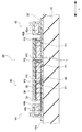
- FIG. 1 is a schematic cross-sectional view showing an example of a solar cell module formed using the scribing method of the embodiment of the present invention.
- 2 (a) to 2 (g) are schematic cross-sectional views showing a method for manufacturing a solar cell module formed using the scribing method of the embodiment of the present invention in the order of steps.
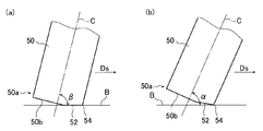
- 3A and 3B are schematic views showing an example of the scribing method according to the embodiment of the present invention.
- the solar cell module 30 shown in FIG. 1 can be formed using the scribing method of the present embodiment.
- the solar cell module 30 is an integrated structure in which solar cells 40 that are photoelectric conversion elements are joined in series.
- the solar cell module 30 includes an insulating substrate 10 (hereinafter simply referred to as a substrate 10) and a plurality of solar cells formed on the surface 10a of the substrate 10 and electrically connected in series in the longitudinal direction L of the substrate 10. 40, a first conductive member 42 connected to one of the plurality of solar cells 40, and a second conductive member 44 connected to the other side.
- the solar cell 40, the first conductive member 42, and the second conductive member 44 are in the width direction orthogonal to the longitudinal direction L of the substrate 10, as in the conventional solar cell 100 (see FIG. 9B). It is the structure extended to W long.
- the substrate 10 of the present embodiment may be exposed to a high temperature exceeding 400 ° C. when the photoelectric conversion layer 34 is formed. Even if the substrate 10 is exposed to this high temperature, the substrate 10 has a predetermined strength. Those that hold are used.
- the substrate 10 for example, soda lime glass, high strain point glass, or non-alkali glass is used.
- the substrate 10 may be a resin substrate or a substrate with an insulating layer in which an electrical insulating layer is formed on the surface of a metal substrate.
- an anodized aluminum plate can be used.
- a substrate 10 in which a stainless steel plate is bonded to an anodized aluminum plate can be used.
- an anodized aluminum plate having an anodized film coated with molybdenum can be used for the substrate 10.
- polyimide may be used for the substrate 10.
- a substrate in which a polyimide base material is coated with molybdenum can be used as the substrate 10. Note that when a substrate coated with molybdenum as described above is used, the coated molybdenum serves as a back electrode.
- a substrate with an insulating layer in which an electric insulating layer is formed on the surface of a metal substrate can be used.
- a JIS 1N99 material purity 99.99 mass% having a thickness of 300 ⁇ m is anodized to form a porous anodic oxide film having a thickness of 5 ⁇ m.
- anodizing treatment for example, an oxalic acid aqueous solution having a concentration of 1 mol / L and a temperature of 55 ° C. is used as the electrolytic bath, and the electrolytic treatment is performed in the electrolytic bath for 5 minutes under a constant voltage condition of 40V.
- NeoCool BD36 manufactured by Yamato Kagaku Co.
- Pear Stirrer PS-100 manufactured by EYELA
- GP0650-2R Teakasago Manufacturing Co., Ltd.
- the substrate 10 of the present embodiment has, for example, a flat plate shape, and the shape, size, and the like are appropriately determined according to the size of the solar cell module 30 to be applied.
- the substrate 10 is, for example, a quadrangular shape or a rectangular shape having a side length exceeding 1 m.
- a back electrode 32, a photoelectric conversion layer 34, a buffer layer 36, and a transparent electrode 38 are sequentially stacked on the front surface 10 a of the substrate 10, and the solar battery cell 40 has a back electrode 32, a photoelectric conversion layer 34, a buffer layer 36, and a transparent electrode.
- the electrode 38 is configured.
- the back electrode 32 is separated from the adjacent back electrode 32 by, for example, a plurality of first separation grooves P1 provided in the longitudinal direction L of the substrate 10 at predetermined intervals.
- the width of the first separation groove P1 is, for example, 50 ⁇ m.
- the photoelectric conversion layer 34 is formed on the back electrode 32 while filling the first separation groove P1.
- a buffer layer 36 is formed on the surface of the photoelectric conversion layer 34.
- a second division groove P2 that penetrates the buffer layer 36 and the photoelectric conversion layer 34 and reaches the surface of the back electrode 34 is formed at a position different from the first separation groove P1.
- a transparent electrode 38 is formed on the buffer layer 36 so as to fill the second dividing groove P2.
- the width of the second separation groove P2 is, for example, 50 ⁇ m.
- a third separation groove P3 that passes through the transparent electrode 38, the buffer layer 36, and the photoelectric conversion layer 34 and reaches the surface of the back electrode 32 is formed at a position different from the first separation groove P1 and the second division groove P2. Yes.
- a plurality of solar cells 40 are formed by the third separation groove P3.
- the width of the third separation groove P3 is, for example, 50 ⁇ m.
- the back electrode 32 and the transparent electrode 38 are both for taking out the current generated in the photoelectric conversion layer 34. Both the back electrode 32 and the transparent electrode 38 are made of a conductive material. The transparent electrode 38 on the light incident side needs to have translucency.
- the back electrode 32 is made of, for example, Mo, Cr, or W and a combination thereof.
- the back electrode 32 may have a single layer structure or a laminated structure such as a two-layer structure.
- the back electrode 32 is preferably composed of Mo.
- the formation method of the back surface electrode 32 is not specifically limited, For example, it can form by vapor phase film-forming methods, such as an electron beam vapor deposition method and a sputtering method.
- the back electrode 32 generally has a thickness of about 800 nm, but the back electrode 32 preferably has a thickness of 400 nm to 1000 nm (1 ⁇ m).
- the film thickness of the back electrode 32 thinner than a general one, the material cost of the back electrode 32 can be reduced, and further, the formation speed of the back electrode 32 can be increased.
- the photoelectric conversion layer 34 is a layer that generates a current by absorbing light that has passed through the transparent electrode 38 and the buffer layer 36, and has a photoelectric conversion function.
- the light absorption layer 34 is composed of, for example, a CIGS film, and the CIGS film is made of a semiconductor having a chalcopyrite crystal structure.
- the composition of the CIGS film is, for example, Cu (In 1-x Ga x ) Se 2 (CIGS).
- CIGS film forming method 1) a multi-source deposition method, 2) a selenization method, 3) a sputtering method, 4) a hybrid sputtering method, and 5) a mechanochemical process method are known.
- Other CIGS film forming methods include screen printing, proximity sublimation, MOCVD, and spray (wet film forming).
- a fine particle film containing an Ib group element, a IIIb group element, and a VIb group element is formed on a substrate by a screen printing method (wet film forming method) or a spray method (wet film forming method), and then pyrolyzed ( At this time, a crystal having a desired composition can be obtained by performing a thermal decomposition treatment in a VIb group element atmosphere (JP-A-9-74065, JP-A-9-74213, etc.).
- a film forming method shows good photoelectric conversion efficiency if CIGS is formed on the substrate as long as the temperature is 500 ° C. or higher, but the process time is short in consideration of manufacturing in a roll-to-roll method. Multisource deposition is preferred.
- the bilayer method is suitable.
- the buffer layer 36 is formed to protect the photoelectric conversion layer 34 when the transparent electrode 38 is formed and to transmit light incident on the transparent electrode 38 to the photoelectric conversion layer 34.
- the buffer layer 36 is made of, for example, a compound containing at least a IIb group element and a VIb group element such as CdS, Zn (O, S, OH), or In (S, OH).
- the buffer layer 36 constitutes a pn junction layer together with the photoelectric conversion layer 34.
- the buffer layer 36 preferably has a thickness of 20 to 100 nm.
- the buffer layer 36 is formed by, for example, a CBD (chemical bath deposition) method.
- the transparent electrode 38 is made of, for example, ZnO doped with Al, B, Ga, In, or the like, or ITO (indium tin oxide).
- the transparent electrode 38 may have a single layer structure or a laminated structure such as a two-layer structure.
- the thickness of the transparent electrode 38 is not particularly limited and is preferably 0.3 to 1 ⁇ m.
- the method for forming the transparent electrode 38 is not particularly limited, and can be formed by a vapor deposition method such as an electron beam evaporation method or a sputtering method.
- a first conductive member 42 is connected on the back electrode 32 at the right end.
- the first conductive member 42 is for taking out an output from a negative electrode to be described later.
- the solar cell 40 is formed on the back electrode 32 at the right end.
- the solar cell 40 is removed by laser scribe or mechanical scribe to expose the back electrode 32.
- the first conductive member 42 is, for example, an elongated belt-like member, extends substantially linearly in the width direction of the substrate 10, and is connected to the right end back electrode 32. As shown in FIG. 1, the first conductive member 42 is, for example, a copper ribbon 42a covered with an indium copper alloy coating 42b. The first conductive member 42 is connected to the back electrode 32 by, for example, ultrasonic soldering.
- the second conductive member 44 is for taking out output from a positive electrode, which will be described later, to the outside.
- the second conductive member 44 is an elongated belt-like member, extends substantially linearly in the width direction of the substrate 10, and is connected to the back electrode 32 at the left end.
- the solar cells 40 are formed on the leftmost back electrode 32.
- the solar cells 40 are removed by mechanical scribing to expose the back electrode 32.
- the second conductive member 44 has the same configuration as the first conductive member 42.
- a copper ribbon 44a is covered with a coating material 44b of indium copper alloy.
- the first conductive member 42 and the second conductive member 44 may be tin-plated copper ribbons.
- the connection between the first conductive member 42 and the second conductive member 44 is not limited to the ultrasonic soldering.
- the first conductive member 42 and the second conductive member 44 may be connected using a conductive adhesive or a conductive tape.
- the solar cell module 30 when light enters the solar cell 40 from the transparent electrode 38 side, this light passes through the transparent electrode 38 and the buffer layer 36, and an electromotive force is generated in the photoelectric conversion layer 34. A current from the transparent electrode 38 toward the back electrode 32 is generated.
- the arrows shown in FIG. 1 indicate the direction of current, and the direction of movement of electrons is opposite to the direction of current. For this reason, in the solar cell 40, the leftmost back electrode 32 in FIG. 1 becomes a positive electrode (plus electrode), and the rightmost back electrode 32 becomes a negative electrode (minus electrode).
- the electric power generated in the solar cell module 30 can be taken out of the solar cell module 30 from the first conductive member 42 and the second conductive member 44.
- the first conductive member 42 is a negative electrode
- the second conductive member 44 is a positive electrode.
- the first conductive member 42 and the second conductive member 44 may have opposite polarities, and appropriately change according to the configuration of the solar cell 40, the configuration of the solar cell module 30, and the like.
- the scribing method of the present embodiment will be specifically described by taking as an example the manufacturing method of the solar cell module 30 shown in FIGS.
- a blade of single crystal diamond is used.
- a molybdenum (Mo) film is formed as the conductive film 12 on the surface of the insulating substrate 10.
- the first separation groove P ⁇ b> 1 is formed in the conductive film 12 by, for example, laser scribing, and the back electrodes 32 separated from each other are formed.
- the CIGS film 14 to be the photoelectric conversion layer 34 is formed by, for example, any one of the above-described CIGS films so as to cover the first separation groove P ⁇ b> 1 and the back electrode 32.
- the CdS film 16 to be the buffer layer 36 is formed on the photoelectric conversion layer 34 by, for example, the CBD (chemical bath deposition) method.
- the CBD chemical bath deposition
- the dividing groove P2 (see FIG. 2E) is formed, and the photoelectric conversion layer 34 and the buffer layer 36 are formed as shown in FIG.
- an Al-doped ZnO (ZnO: Al) film 18 (hereinafter simply referred to as ZnO film 18) to be the transparent electrode 38 is formed by, for example, sputtering using a buffer layer. It is formed so as to fill the second dividing groove P ⁇ b> 2 on 36.
- ZnO film 18 an Al-doped ZnO (ZnO: Al) film 18 (hereinafter simply referred to as ZnO film 18) to be the transparent electrode 38 is formed by, for example, sputtering using a buffer layer. It is formed so as to fill the second dividing groove P ⁇ b> 2 on 36.
- a third dividing groove P3 (see FIG. 2G) is formed.
- the transparent electrode 38 is formed, and a plurality of solar cells 40 connected in series in the longitudinal direction L of the substrate 10 are formed. In this way, the solar cell module 30 is formed.
- the second dividing groove P2 and the third dividing groove P3 are formed by the scribing method of the present embodiment.
- the scribing method of this embodiment will be described.
- a chamfered portion 52 is formed at the tip 50 a of the blade 50 having a uniform width.
- a state in which the chamfered portion 52 is formed on the blade edge 50 is referred to as a new blade.
- a state where the chamfered portion 52 is not formed is a new blade.
- the workpieces in the scribing method of the present invention are all those that are above the back electrode 32 of the solar cell module 30.
- examples of the workpiece include the photoelectric conversion layer 34 (CIGS film 14), the buffer layer 36 (CdS film 16), and the transparent electrode 38 (ZnO film 18).
- the antireflection layer or the like is also included in the workpiece.
- the chamfered portion 52 is formed in advance by chamfering a part of the end surface 50b of the tip 50a of the cutting edge 50, for example.
- the end surface 50b of the blade edge 50 is used as a work material for aging at a specified angle.
- the chamfered portion 52 may be formed by chamfering a part of the end surface 50b of the blade edge 50 by pressing it at (angle ⁇ ) and moving the blade edge 50 while maintaining the specified angle (angle ⁇ ).
- the edge portion 134 of the cutting edge 130 has a significant initial wear and slip, resulting in poor scribe groove formation.
- the amount of wear on the blade edge is not proportional to the scribe distance as shown in FIG. 4 (a), but is somewhat proportional to the scribe distance. It was found that as the wear progresses, the wear does not progress any further. Further, as shown in FIG. 4B, it has been found that the blade edge area does not increase when the scribe distance reaches a certain level, similarly to the wear amount. Furthermore, as shown in FIG. 4C, it has been found that the cutting edge load does not decrease when the cutting edge load reaches a certain scribe distance as in the wear amount.
- a blade having a chamfered portion 52 previously formed on the cutting edge 50 is used as a new blade, and the cutting edge having such a form is used. Used for scribe.
- the relationship between the initial wear amount of the blade edge and the scribe distance shown in FIG. 4A, the relationship between the blade edge area and the scribe distance shown in FIG. 4B, and the relationship between the blade edge load and the scribe distance shown in FIG. All are the results obtained by using single crystal diamond for the cutting edge.
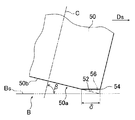
- the initial wear amount shown in FIG. 4A is, as shown in FIG. 5, the chamfered portion 52 formed on the end face 50b of the blade edge 50 in a state where the blade edge 50 is set to the angle ⁇ at the time of scribing. It is the length in the direction parallel to the surface Bs of the workpiece B.
- Reference numeral 56 shown in FIG. 5 indicates a chamfered portion.
- the initial wear amount shown in FIG. 4A and the chamfering amount ⁇ of the chamfered portion 52 are the same.
- the angle ⁇ (specified angle) at the time of scribing is an angle formed by the center line C of the blade edge 50 and the surface of the workpiece B. This angle ⁇ is preferably 60 ° or more and less than 90 °.
- the amount of change due to initial wear is flat, and the point where no further wear is 6 ⁇ m.
- the point where no further wear is 6 ⁇ m.
- the upper limit value of the chamfering amount ⁇ is preferably about the initial wear amount plus several ⁇ m.
- the chamfering amount ⁇ of the chamfered portion 52 is, for example, 5 ⁇ m to 50 ⁇ m, and preferably 10 ⁇ m to 50 ⁇ m.
- the load on the blade edge 50 is preferably 0.1N to 2.0N.
- the chamfering amount ⁇ is less than 5 ⁇ m, wear of the chamfered portion 52 proceeds and the scribe may become unstable.
- the chamfering amount ⁇ exceeds 50 ⁇ m, the surface pressure decreases, and slipping easily occurs during scribing.
- the load on the cutting edge 50 is less than 0.1 N, the pressing force on the workpiece is small and it is difficult to cut and it is difficult to form a groove.
- the load of the blade edge 50 exceeds 2.0 N, there is a possibility that the back electrode 32 may be damaged due to a high load.
- the chamfering amount ⁇ varies depending on the width of the blade edge 50 and the material of the blade edge 50.
- the cutting edge 50 is made of, for example, single crystal diamond, but is also made of polycrystalline diamond, sapphire, ceramics, super steel, or the like. Further, the width of the blade edge 50 (the chamfered portion 52) is appropriately set according to the width of the groove to be formed.
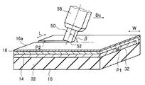
- the blade edge 50 is held by a holder 58 as shown in FIG.
- the holder 58 is attached to a moving mechanism that moves the blade edge 50 in the scribe direction Ds.
- This moving mechanism has a function of controlling the force that presses the cutting edge 50 against the workpiece, that is, the load applied by the cutting edge 50.
- the moving mechanism includes a swing mechanism, and the angle of the blade edge 50 can be set to an arbitrary angle.
- the well-known moving mechanism utilized for the scribe for manufacturing a solar cell can be used as a moving mechanism.
- the second dividing groove P2 and the third dividing groove P3 are formed with a predetermined interval in the longitudinal direction L.
- the substrate 10 is moved in the longitudinal direction L by the substrate transport mechanism that moves in the longitudinal direction L, and the position of the cutting edge 50 and the formation position of the second divided groove P2 or the third divided groove P3 is matched,
- the moving mechanism moves the cutting edge 50 in the scribe direction Ds to form the second divided groove P2 and the third divided groove P3.
- the scribe direction Ds is parallel to the width direction W of the substrate 10.
- the second dividing groove P2 and the third dividing groove P3 may be formed one by one, or a plurality of blades may be arranged to form a plurality of rows.
- the cutting edge 50 is set at an angle ⁇ by a moving mechanism (not shown), and the CdS film 16 serving as the buffer layer 36 is formed.
- the chamfered portion 52 is pressed against the second dividing groove P2 formation region of the front surface 16a, the chamfered portion 52 is cut through the CIGS film 14 serving as the photoelectric conversion layer 34 until reaching the surface of the back electrode 32, and the cutting edge 50 is scribed.
- the second dividing groove P2 is formed by moving in the direction Ds, that is, the width direction W (scribing step).
- the third dividing groove P3 formation region on the surface of the ZnO film 18 to be the transparent electrode 38 is moved by a moving mechanism (not shown) in the same manner as the second dividing groove P2.
- the chamfered portion 52 is pressed against the back electrode 32 through the CdS film 16 serving as the buffer layer 36 and the CIGS film 14 serving as the photoelectric conversion layer 34, and the cutting edge 50 is scribed in the scribe direction.
- the third dividing groove P3 is formed by moving in Ds, that is, the width direction W (scribing step).
- the high-quality second separation groove P2 and third separation groove P3 free from slip and the like are formed on the solar cell module 30. It can be formed stably throughout. In particular, when the size of the solar cell module 30 is increased, the total distance between the second separation groove P2 and the third separation groove P3 becomes longer, so the scribing method of this embodiment is effective.
- the method is simply limited to a method of scribing by pressing the workpiece B such as the buffer layer 36 (CdS film 16) and the transparent electrode 38 (ZnO film 18) and moving it in the scribe direction Ds. Is not to be done.
- the blade edge 50 has an angle ⁇ tilted to the scribe direction Ds side by, for example, 5 ° to 10 ° from the angle ⁇ during scribing.
- the end portion 54 of the blade edge 50 is pressed against the scribe start point of the workpiece B.
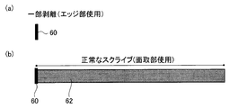
- Fig.7 (a) a part of workpiece B is peeled and the peeling part 60 is formed (cut formation process). This peeling part 60 is an initial cut.
- the cutting edge 50 is once separated from the workpiece B by a moving mechanism (not shown), and the cutting edge 50 is set to an angle ⁇ during scribing as shown in FIG.
- the chamfered portion 52 is pressed against the surface, and the cutting edge 50 is moved in the scribe direction Ds (scribing step).
- a scribe groove 62 is formed following the peeling portion 60 (initial cut).
- the second separation groove P2 and the third separation groove P3 can be formed.
- the peeling portion 60 at the scribe start point the initial cut is formed, the biting of the cutting edge 50 is improved, and a large load required for the cut is not required.
- the pressing force to the workpiece B when the chamfered portion 52 is brought into contact and scribed can be reduced. Therefore, scribing is possible with a low load, wear of the chamfered portion 52 of the cutting edge can be suppressed, damage such as chipping of the cutting edge 50 can be suppressed, and the tool life of the cutting edge 50 can be extended. .
- the blade edge 50 is inclined, for example, 5 ° to 10 ° with respect to the angle ⁇ at the time of scribing, and this angle presses the end portion 54 against the workpiece B. If it can, it will not be specifically limited. It can be appropriately changed according to the form of the chamfered portion 52.
- the shape of the blade edge is not limited to a constant width as shown in FIG.
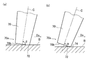
- a tapered cutting edge with a narrow end as shown in FIG. 8A may be used, and even in this case, the same effect as the cutting edge 50 shown in FIG. 3A can be obtained.
- a chamfered portion 72 is formed at the end portion 70 b of the tip end portion 70 a. Since the chamfered portion 72 has the same configuration as the chamfered portion 52 on the cutting edge 50, a detailed description thereof will be omitted. Further, since the angle ⁇ at the time of scribing is the same as that of the cutting edge 50, detailed description thereof is omitted.
- the present invention is basically configured as described above.
- the scribing method of the present invention has been described in detail above.
- the present invention is not limited to the above-described embodiment, and various improvements or modifications may be made without departing from the spirit of the present invention. .
Landscapes
- Photovoltaic Devices (AREA)
- Processing Of Stones Or Stones Resemblance Materials (AREA)
- Milling, Broaching, Filing, Reaming, And Others (AREA)
Description
本発明は、太陽電池サブモジュールの製造に利用されるスクライブ方法に関し、特に、長期に亘り安定したスクライブが可能であるとともに、用いられる刃の寿命を長寿命化できるスクライブ方法に関する。
現在、太陽電池の研究が盛んに行われている。太陽電池は、光吸収により電流を発生する半導体の光電変換層を裏面電極と透明電極とで挟んだ積層構造を有する太陽電池セルが絶縁性基板上に多数直列に接続されて構成されている。
太陽電池としては、光電変換層にカルコパイライト系のCuInSe2(CIS)、Cu(In,Ga)Se2(以下、単にCIGSともいう)を用いたものが検討されている。CIGS膜を光電変換層に用いた太陽電池は、効率が比較的高く、光吸収率が高いため薄膜化できることから、盛んに研究されている。
太陽電池としては、光電変換層にカルコパイライト系のCuInSe2(CIS)、Cu(In,Ga)Se2(以下、単にCIGSともいう)を用いたものが検討されている。CIGS膜を光電変換層に用いた太陽電池は、効率が比較的高く、光吸収率が高いため薄膜化できることから、盛んに研究されている。
従来の太陽電池は、例えば、図9(a)に示す構成のものが知られており、以下に示す集積化工程を経て集積化構造とされる。
図9(a)に示す太陽電池100においては、絶縁性基板110の表面に、例えば、第1の分離溝P1が形成されて互いに分離されたMo層からなる裏面電極112が形成されている。
第1の分離溝P1および裏面電極112を覆うように、CIGS層からなる光電変換層114が形成されている。この光電変換層114上に、CdS層からなるバッファ層116が形成されている。
図9(a)に示す太陽電池100においては、絶縁性基板110の表面に、例えば、第1の分離溝P1が形成されて互いに分離されたMo層からなる裏面電極112が形成されている。
第1の分離溝P1および裏面電極112を覆うように、CIGS層からなる光電変換層114が形成されている。この光電変換層114上に、CdS層からなるバッファ層116が形成されている。
第1の分離溝P1とは異なる位置に、メカニカルスクライブにより、バッファ層116から裏面電極112に達する第2の分離溝P2が形成されている。この第2の分離溝P2により、光電変換層114およびバッファ層116が分割されている。
バッファ層116を覆い、かつ第2の分離溝P2を埋めるようにして、AZO(Al2O3:ZnO)からなる透明電極118が形成されている。第1の分離溝P1および第2の分離溝P2とは異なる位置に、透明電極118から裏面電極112に達する第3の分離溝P3が、例えば、メカニカルスクライブにより形成されている。
第3の分離溝P3により分離された裏面電極112、光電変換層114、バッファ層116および透明電極118により、太陽電池セル120が構成される。
太陽電池セル120は、例えば、図9(b)に示すように、絶縁性基板110の幅方向Wに長く伸びるように形成されている。また、太陽電池セル120は、縁性基板110の長手方向Lにおいて隣接する太陽電池セル120と直列に接続されている。
第1の分離溝P1、第2の分離溝P2、第3の分離溝P3は、それぞれ幅が約30~60μmの微細な溝である。
第3の分離溝P3により分離された裏面電極112、光電変換層114、バッファ層116および透明電極118により、太陽電池セル120が構成される。
太陽電池セル120は、例えば、図9(b)に示すように、絶縁性基板110の幅方向Wに長く伸びるように形成されている。また、太陽電池セル120は、縁性基板110の長手方向Lにおいて隣接する太陽電池セル120と直列に接続されている。
第1の分離溝P1、第2の分離溝P2、第3の分離溝P3は、それぞれ幅が約30~60μmの微細な溝である。
上述のように、従来の太陽電池100の集積化プロセスでは、約30~60μmの微細な溝を形成するためにメカニカルスクライブ装置を使用して加工している。
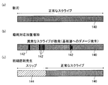
図10(a)に示すように、刃先130が新しい場合を用いて被加工物Bをスクライブする場合、すなわち、新刃の場合には、図11(a)に示すように、正常なスクライブが可能であり、正常なスクライブ領域140が得られ、所定のスクライブ溝が形成される。
図10(a)に示すように、刃先130が新しい場合を用いて被加工物Bをスクライブする場合、すなわち、新刃の場合には、図11(a)に示すように、正常なスクライブが可能であり、正常なスクライブ領域140が得られ、所定のスクライブ溝が形成される。
しかし、新刃時等に刃先のエッジ部分134を使用すると、次の様な問題が生じる。新刃のエッジ部分134は初期磨耗が著しく、図10(b)に示すように面取部132が形成され、それに伴う接触面積の増加による面圧低下が起こる。これにより、スリップが発生してスクライブ溝の形成不良が発生する。このスクライブ溝の形成不良の発生を抑制するために、荷重コントロールのメンテナンスが必要となり、スクライブの稼動に影響が及ぶ。これを解決するために、従来、特許文献1に示すスクライブ装置が提案されている。
特許文献1には、筒体の先方が所定のテーパ角度をもって先細りになり、その先細りの先端が平坦になった刃を所定の圧力をもって被加工面のスクライブ箇所に垂直に押し付けて、その刃を被加工面に沿って移動させることによってスクライブ加工を施す手段と、刃の先端の平坦部分の大きさを測定する手段と、その測定された平坦部分の大きさに応じて刃の押圧力を制御する手段とによって構成されたメカニカルスクライブ装置が開示されている。刃の先端の平坦部分の大きさを測定する手段は、カメラ部をそなえ、そのカメラ部により刃先端の平坦部分の大きさを測定するようにしている。このように、特許文献1では、カメラで先端部を観察して刃の押圧力を制御している。
特許文献1にも開示されているように、初期磨耗が発生した状態で、刃の押圧をコントロールした場合、刃先の面積が大きくなると対応する荷重も大きくなる。しかし、荷重が大きくなると従来の太陽電池100の絶縁性基板110に変形等の影響が生じ、図11(b)に示すように、異常スクライブ領域142が散発して発生する。一方、荷重を下げると、図11(c)に示すように、スクライブ開始初期にスリップ領域144が発生して、加工不良を起してしまうという問題がある。
このように、従来のスクライブ方法では、新刃の状態から長期に亘り安定したスクライブができないのが現状である。
このように、従来のスクライブ方法では、新刃の状態から長期に亘り安定したスクライブができないのが現状である。
本発明の目的は、前記従来技術に基づく問題点を解消し、長期に亘り安定したスクライブが可能であるスクライブ方法を提供することにある。
上記目的を達成するために、本発明は、被加工物に刃先を規定角度で押し当てて、規定角度を保った状態で刃先を所定のスクライブ方向に移動させて被加工物に溝を形成するスクライブ工程を有し、刃先の先端部は、予めエージングするか、または面取り加工を施すことにより面取りされていることを特徴とするスクライブ方法を提供するものである。
スクライブ工程の前に、刃先を用いて被加工物の溝形成開始位置に切り込みを形成する切込形成工程を有し、切り込みを形成した後、刃先を被加工物から離間させた後、スクライブ工程に移行することが好ましい。
また、切込形成工程は、スクライブ工程での刃先の角度よりもスクライブ方向側に傾けて溝形成開始位置に切り込みを形成することが好ましい。
また、切込形成工程は、スクライブ工程での刃先の角度よりもスクライブ方向側に傾けて溝形成開始位置に切り込みを形成することが好ましい。
例えば、刃先の先端部の面取り量は、5μm~50μmである。
また、例えば、スクライブ工程での刃先の角度は、60°以上90°未満である。さらには、例えば、切込形成工程において刃先をスクライブ方向側に傾ける角度は、5°~10°である。
また、例えば、スクライブ工程での刃先の角度は、60°以上90°未満である。さらには、例えば、切込形成工程において刃先をスクライブ方向側に傾ける角度は、5°~10°である。
本発明によれば、刃先の先端部を、予めエージング、または面取り加工によって面取りすることにより、長期に亘り安定したスクライブが可能である。また、初期摩耗により発生するスリップが抑制され、溝の品質の悪化、それに伴う条件設定の変更と稼働ロスも削減することができる。
さらには、溝形成開始位置に切り込みを形成することにより、低荷重で溝を形成することができる。これにより、刃先の摩耗、および刃先の欠け等の損傷を抑制することができ、ひいては刃先の長寿命化を図ることができる。
さらには、溝形成開始位置に切り込みを形成することにより、低荷重で溝を形成することができる。これにより、刃先の摩耗、および刃先の欠け等の損傷を抑制することができ、ひいては刃先の長寿命化を図ることができる。
以下、添付の図面に示す好適実施形態に基づいて、本発明のスクライブ方法を詳細に説明する。
図1は、本発明の実施形態のスクライブ方法を用いて形成される太陽電池モジュールの一例を示す模式的断面図である。図2(a)~(g)は、本発明の実施形態のスクライブ方法を用いて形成される太陽電池モジュールの製造方法を工程順に示す模式的断面図である。図3(a)、(b)は、それぞれ本発明の実施形態のスクライブ方法の一例を示す模式図である。
図1は、本発明の実施形態のスクライブ方法を用いて形成される太陽電池モジュールの一例を示す模式的断面図である。図2(a)~(g)は、本発明の実施形態のスクライブ方法を用いて形成される太陽電池モジュールの製造方法を工程順に示す模式的断面図である。図3(a)、(b)は、それぞれ本発明の実施形態のスクライブ方法の一例を示す模式図である。
本実施形態のスクライブ方法を用いて、例えば、図1に示す太陽電池モジュール30を形成することができる。
まず、図1に示す太陽電池モジュール30について説明する。太陽電池モジュール30は、光電変換素子である太陽電池セル40が直列に接合された集積構造体である。
太陽電池モジュール30は、絶縁性基板10(以下、単に基板10という)と、この基板10の表面10aに形成され、基板10の長手方向Lにおいて電気的に直列に接続された複数の太陽電池セル40、複数の太陽電池セル40の一方に接続される第1の導電部材42、およびその他方に接続される第2の導電部材44を有する。
なお、太陽電池セル40、第1の導電部材42および第2の導電部材44は、従来の太陽電池100(図9(b)参照)と同様に、基板10の長手方向Lと直交する幅方向Wに長く伸びた構成である。
まず、図1に示す太陽電池モジュール30について説明する。太陽電池モジュール30は、光電変換素子である太陽電池セル40が直列に接合された集積構造体である。
太陽電池モジュール30は、絶縁性基板10(以下、単に基板10という)と、この基板10の表面10aに形成され、基板10の長手方向Lにおいて電気的に直列に接続された複数の太陽電池セル40、複数の太陽電池セル40の一方に接続される第1の導電部材42、およびその他方に接続される第2の導電部材44を有する。
なお、太陽電池セル40、第1の導電部材42および第2の導電部材44は、従来の太陽電池100(図9(b)参照)と同様に、基板10の長手方向Lと直交する幅方向Wに長く伸びた構成である。
本実施形態の基板10は、太陽電池モジュール30を製造する際に、光電変換層34の形成時に400℃を超えるような高温に曝されることがあり、この高温に曝されても所定の強度を保持するものが用いられる。基板10には、例えば、ソーダライムガラス、高歪点ガラス、または無アルカリガラスが用いられる。また、基板10に、樹脂基板、または金属基板の表面に電気絶縁層が形成された絶縁層付基板を用いることもできる。
基板10には、陽極酸化処理されたアルミニウム板を用いることもできる。また、陽極酸化処理されたアルミニウム板にステンレス鋼板を貼り合わせたものを基板10に用いることができる。さらには、陽極酸化処理されたアルミニウム板の陽極酸化膜にモリブデンがコーティングされたものを基板10に用いることができる。
この他、基板10には、ポリイミドを用いることもできる。また、基板10に、ポリイミド基材にモリブデンがコーティングされたものを用いることもできる。なお、上述のようにモリブデンがコーティングされた基板を用いる場合、コーティングされたモリブデンが裏面電極となる。
基板10には、陽極酸化処理されたアルミニウム板を用いることもできる。また、陽極酸化処理されたアルミニウム板にステンレス鋼板を貼り合わせたものを基板10に用いることができる。さらには、陽極酸化処理されたアルミニウム板の陽極酸化膜にモリブデンがコーティングされたものを基板10に用いることができる。
この他、基板10には、ポリイミドを用いることもできる。また、基板10に、ポリイミド基材にモリブデンがコーティングされたものを用いることもできる。なお、上述のようにモリブデンがコーティングされた基板を用いる場合、コーティングされたモリブデンが裏面電極となる。
基板10には、金属基板の表面に電気絶縁層が形成された絶縁層付基板を用いることもできる。この絶縁層付基板としては、例えば、厚さが300μmのJIS 1N99材(純度99.99質量%)を陽極酸化処理して、厚さが5μmのポーラス構造の陽極酸化膜が形成されたものを用いることができる。
陽極酸化処理としては、例えば、電解浴として、濃度が1mol/L、温度55℃のシュウ酸水溶液を用い、電解浴中で、電圧40Vの定電圧条件で5分間電解処理がなされる。なお、陽極酸化処理中、電流密度は、特に制御しなかったが陽極酸化処理中の平均値で約10A/dm2であった。
なお、陽極酸化処理には、例えば、冷却装置として、NeoCool BD36(ヤマト科学社製)、撹拌加温装置として、ペアスターラーPS-100(EYELA社製)、電源として、GP0650-2R(高砂製作所社製)を用いることができる。
陽極酸化処理としては、例えば、電解浴として、濃度が1mol/L、温度55℃のシュウ酸水溶液を用い、電解浴中で、電圧40Vの定電圧条件で5分間電解処理がなされる。なお、陽極酸化処理中、電流密度は、特に制御しなかったが陽極酸化処理中の平均値で約10A/dm2であった。
なお、陽極酸化処理には、例えば、冷却装置として、NeoCool BD36(ヤマト科学社製)、撹拌加温装置として、ペアスターラーPS-100(EYELA社製)、電源として、GP0650-2R(高砂製作所社製)を用いることができる。
本実施形態の基板10は、例えば、平板状であり、その形状および大きさ等は適用される太陽電池モジュール30の大きさ等に応じて適宜決定されるものである。
基板10は、例えば、一辺の長さが1mを超える四角形状または矩形状である。
基板10は、例えば、一辺の長さが1mを超える四角形状または矩形状である。
基板10の表面10aに裏面電極32と光電変換層34とバッファ層36と透明電極38とが順次積層されており、太陽電池セル40は、裏面電極32、光電変換層34、バッファ層36および透明電極38により構成される。
裏面電極32は、例えば、基板10の長手方向Lに、所定の間隔に複数設けられた第1の分離溝P1により、隣り合う裏面電極32と互いに分離されている。なお、第1の分離溝P1の幅は、例えば、50μmである。
光電変換層34は、第1の分離溝P1を埋めつつ裏面電極32の上に形成されている。この光電変換層34の表面にバッファ層36が形成されている。バッファ層36および光電変換層34を貫き裏面電極34の表面に達する第2の分割溝P2が、第1の分離溝P1とは異なる位置に形成されている。このバッファ層36上に、第2の分割溝P2を埋めるようにして透明電極38が形成されている。なお、第2の分離溝P2の幅は、例えば、50μmである。
光電変換層34は、第1の分離溝P1を埋めつつ裏面電極32の上に形成されている。この光電変換層34の表面にバッファ層36が形成されている。バッファ層36および光電変換層34を貫き裏面電極34の表面に達する第2の分割溝P2が、第1の分離溝P1とは異なる位置に形成されている。このバッファ層36上に、第2の分割溝P2を埋めるようにして透明電極38が形成されている。なお、第2の分離溝P2の幅は、例えば、50μmである。
透明電極38、バッファ層36および光電変換層34を貫き裏面電極32の表面に達する第3の分離溝P3が、第1の分離溝P1および第2の分割溝P2とは異なる位置に形成されている。この第3の分離溝P3により、複数の太陽電池セル40が形成される。なお、第3の分離溝P3の幅は、例えば、50μmである。
太陽電池セル40において、裏面電極32および透明電極38は、いずれも光電変換層34で発生した電流を取り出すためのものである。裏面電極32および透明電極38は、いずれも導電性材料からなる。光入射側の透明電極38は透光性を有する必要がある。
裏面電極32は、例えば、Mo、Cr、またはW、およびこれらを組合わせたものにより構成される。この裏面電極32は、単層構造でもよいし、2層構造等の積層構造でもよい。裏面電極32は、Moで構成することが好ましい。
また、裏面電極32の形成方法は、特に制限されるものではなく、例えば、電子ビーム蒸着法、およびスパッタ法等の気相成膜法により形成することができる。
また、裏面電極32の形成方法は、特に制限されるものではなく、例えば、電子ビーム蒸着法、およびスパッタ法等の気相成膜法により形成することができる。
裏面電極32は、一般的に厚さが800nm程度であるが、裏面電極32は、厚さが400nm~1000nm(1μm)であることが好ましい。このように裏面電極32の膜厚を一般的なものよりも薄くすることにより、裏面電極32の材料費を削減でき、さらには裏面電極32の形成速度も速くすることができる。
光電変換層34は、透明電極38およびバッファ層36を通過して到達した光を吸収して電流が発生する層であり、光電変換機能を有する。
光吸収層34は、例えば、CIGS膜で構成されており、CIGS膜はカルコパイライト結晶構造を有する半導体からなる。CIGS膜の組成は、例えば、Cu(In1-xGax)Se2(CIGS)である。
光吸収層34は、例えば、CIGS膜で構成されており、CIGS膜はカルコパイライト結晶構造を有する半導体からなる。CIGS膜の組成は、例えば、Cu(In1-xGax)Se2(CIGS)である。
CIGS膜の形成方法としては、1)多源蒸着法、2)セレン化法、3)スパッタ法、4)ハイブリッドスパッタ法、および5)メカノケミカルプロセス法等が知られている。
その他のCIGSの成膜法としては、スクリーン印刷法、近接昇華法、MOCVD法、およびスプレー法(ウェット成膜法)等が挙げられる。例えば、スクリーン印刷法(ウェット成膜法)またはスプレー法(ウェット成膜法)等で、Ib族元素、IIIb族元素、およびVIb族元素を含む微粒子膜を基板上に形成し、熱分解処理(この際、VIb族元素雰囲気での熱分解処理でもよい)を実施する等により、所望の組成の結晶を得ることができる(特開平9-74065号公報、特開平9-74213号公報等)。
このような成膜方法は、基板上でCIGSを形成する際にいずれも500℃以上であれば、良好な光電変換効率を示すが、ロールツーロール方式での製造を考慮すると、プロセス時間が短い多源蒸着法が好ましい。とりわけ、バイレイヤー法が好適である。
その他のCIGSの成膜法としては、スクリーン印刷法、近接昇華法、MOCVD法、およびスプレー法(ウェット成膜法)等が挙げられる。例えば、スクリーン印刷法(ウェット成膜法)またはスプレー法(ウェット成膜法)等で、Ib族元素、IIIb族元素、およびVIb族元素を含む微粒子膜を基板上に形成し、熱分解処理(この際、VIb族元素雰囲気での熱分解処理でもよい)を実施する等により、所望の組成の結晶を得ることができる(特開平9-74065号公報、特開平9-74213号公報等)。
このような成膜方法は、基板上でCIGSを形成する際にいずれも500℃以上であれば、良好な光電変換効率を示すが、ロールツーロール方式での製造を考慮すると、プロセス時間が短い多源蒸着法が好ましい。とりわけ、バイレイヤー法が好適である。
バッファ層36は、透明電極38の形成時の光電変換層34を保護すること、透明電極38に入射した光を光電変換層34まで透過させるために形成されたものである。
バッファ層36は、例えば、CdS、Zn(O、S、OH)、またはIn(S、OH)等の少なくともIIb族元素およびVIb族元素を含む化合物により構成される。このバッファ層36は、光電変換層34とともにpn接合層を構成する。
バッファ層36は、その厚さが、20~100nmであることが好ましい。また、このバッファ層36は、例えば、CBD(ケミカルバスデポジション)法により形成される。
バッファ層36は、例えば、CdS、Zn(O、S、OH)、またはIn(S、OH)等の少なくともIIb族元素およびVIb族元素を含む化合物により構成される。このバッファ層36は、光電変換層34とともにpn接合層を構成する。
バッファ層36は、その厚さが、20~100nmであることが好ましい。また、このバッファ層36は、例えば、CBD(ケミカルバスデポジション)法により形成される。
透明電極38は、例えば、Al、B、Ga、もしくはIn等がドープされたZnO、またはITO(インジウム錫酸化物)により構成される。この透明電極38は、単層構造でもよいし、2層構造等の積層構造でもよい。また、透明電極38の厚さは、特に制限されるものではなく、0.3~1μmが好ましい。
また、透明電極38の形成方法は、特に制限されるものではなく、電子ビーム蒸着法、スパッタ法等の気相成膜法により形成することができる。
また、透明電極38の形成方法は、特に制限されるものではなく、電子ビーム蒸着法、スパッタ法等の気相成膜法により形成することができる。
図1に示すように、右側の端の裏面電極32上に第1の導電部材42が接続されている。この第1の導電部材42は、後述する負極からの出力を外部に取り出すためのものである。本来、右側の端の裏面電極32上には太陽電池セル40が形成されるが、例えば、レーザースクライブまたはメカニカルスクライブにより、太陽電池セル40を取り除いて、裏面電極32を表出させている。
第1の導電部材42は、例えば、細長い帯状の部材であり、基板10の幅方向に略直線状に伸びて、右端の裏面電極32上に接続されている。また、図1に示すように、第1の導電部材42は、例えば、銅リボン42aがインジウム銅合金の被覆材42bで被覆されたものである。この第1の導電部材42は、例えば、超音波半田により裏面電極32に接続される。
この第2の導電部材44は、後述する正極からの出力を外部に取り出すためのものである。第2の導電部材44も、第1の導電部材42と同様に細長い帯状の部材であり、基板10の幅方向に略直線状に伸びて、左端の裏面電極32に接続されている。本来、左端の裏面電極32上には太陽電池セル40が形成されるが、例えば、メカニカルスクライブにより、太陽電池セル40を取り除いて、裏面電極32を表出させている。
第2の導電部材44は、第1の導電部材42と同様の構成のものであり、例えば、銅リボン44aがインジウム銅合金の被覆材44bで被覆されたものである。
第1の導電部材42と第2の導電部材44とは、錫メッキ銅リボンでもよい。また、第1の導電部材42および第2の導電部材44、それぞれの接続も超音波半田に限定されるものではなく、例えば、導電性接着剤、導電性テープを用いて接続してもよい。
第1の導電部材42と第2の導電部材44とは、錫メッキ銅リボンでもよい。また、第1の導電部材42および第2の導電部材44、それぞれの接続も超音波半田に限定されるものではなく、例えば、導電性接着剤、導電性テープを用いて接続してもよい。
太陽電池モジュール30では、太陽電池セル40に、透明電極38側から光が入射されると、この光が透明電極38およびバッファ層36を通過し、光電変換層34で起電力が発生し、例えば、透明電極38から裏面電極32に向かう電流が発生する。なお、図1に示す矢印は、電流の向きを示すものであり、電子の移動方向は、電流の向きとは逆になる。このため、太陽電池セル40では、図1中、左端の裏面電極32が正極(プラス極)になり、右端の裏面電極32が負極(マイナス極)になる。
本実施形態において、太陽電池モジュール30で発生した電力を、第1の導電部材42と第2の導電部材44から、太陽電池モジュール30の外部に取り出すことができる。
なお、本実施形態において、第1の導電部材42が負極であり、第2の導電部材44が正極である。また、第1の導電部材42と第2の導電部材44とは極性が逆であってもよく、太陽電池セル40の構成、太陽電池モジュール30構成等に応じて適宜変わるものである。
なお、本実施形態において、第1の導電部材42が負極であり、第2の導電部材44が正極である。また、第1の導電部材42と第2の導電部材44とは極性が逆であってもよく、太陽電池セル40の構成、太陽電池モジュール30構成等に応じて適宜変わるものである。
次に、本実施形態のスクライブ方法について、具体的には、図2(a)~(g)に示す太陽電池モジュール30の製造方法を例にして説明する。なお、本実施形態のスクライブ方法では、後に詳細に説明するが、例えば、単結晶ダイヤモンドの刃先が用いられる。
まず、図2(a)に示すように、絶縁性基板10の表面に、導電膜12として、例えば、モリブデン(Mo)膜を形成する。
次に、図2(b)に示すように、導電膜12に、例えば、レーザースクライブにより第1の分離溝P1を形成して、互いに分離された裏面電極32を形成する。
次に、図2(c)に示すように、第1の分離溝P1および裏面電極32を覆うように、光電変換層34となるCIGS膜14を、例えば、上述のCIGS膜のいずれかの方法で形成する。
まず、図2(a)に示すように、絶縁性基板10の表面に、導電膜12として、例えば、モリブデン(Mo)膜を形成する。
次に、図2(b)に示すように、導電膜12に、例えば、レーザースクライブにより第1の分離溝P1を形成して、互いに分離された裏面電極32を形成する。
次に、図2(c)に示すように、第1の分離溝P1および裏面電極32を覆うように、光電変換層34となるCIGS膜14を、例えば、上述のCIGS膜のいずれかの方法で形成する。
次に、図2(d)に示すように、この光電変換層34上に、バッファ層36となるCdS膜16を、例えば、CBD(ケミカルバスデポジション)法で形成する。
次に、以下に詳細に説明する本実施形態のスクライブ方法を用いて、第1の分離溝P1とは異なる位置に、CdS膜16からCIGS膜14を経て裏面電極32の表面に達する第2の分割溝P2(図2(e)参照)を形成し、図2(e)に示すように光電変換層34およびバッファ層36を形成する。
次に、以下に詳細に説明する本実施形態のスクライブ方法を用いて、第1の分離溝P1とは異なる位置に、CdS膜16からCIGS膜14を経て裏面電極32の表面に達する第2の分割溝P2(図2(e)参照)を形成し、図2(e)に示すように光電変換層34およびバッファ層36を形成する。
次に、図2(f)に示すように、透明電極38となる、AlがドープされたZnO(ZnO:Al)膜18(以下、単にZnO膜18という)を、例えば、スパッタ法でバッファ層36上に第2の分割溝P2を埋めるようにして形成する。
次に、本実施形態のスクライブ方法を用いて、第1の分離溝P1および第2の分割溝P2とは異なる位置に、ZnO膜18、CdS膜16およびCIGS膜14を経て裏面電極32の表面に達する第3の分割溝P3(図2(g)参照)を形成する。これにより、図2(g)に示すように、透明電極38が形成されるとともに、基板10の長手方向Lに直列接続された複数の太陽電池セル40が形成される。このようにして、太陽電池モジュール30が形成される。
次に、本実施形態のスクライブ方法を用いて、第1の分離溝P1および第2の分割溝P2とは異なる位置に、ZnO膜18、CdS膜16およびCIGS膜14を経て裏面電極32の表面に達する第3の分割溝P3(図2(g)参照)を形成する。これにより、図2(g)に示すように、透明電極38が形成されるとともに、基板10の長手方向Lに直列接続された複数の太陽電池セル40が形成される。このようにして、太陽電池モジュール30が形成される。
上述のように第2の分割溝P2および第3の分割溝P3は、本実施形態のスクライブ方法により形成される。以下、本実施形態のスクライブ方法について説明する。
スクライブ方法には、図3(a)に示すように、等幅の刃先50の先端部50aに面取部52が形成されたものが用いられる。本発明では、刃先50に面取部52が形成された状態を新刃という。一方、従来では、図10(a)に示すように、面取部52が形成されていない状態を新刃としている。
また、本発明のスクライブ方法における被加工物とは、太陽電池モジュール30の裏面電極32よりも上層にある全てのものである。このため、被加工物としては、例えば、光電変換層34(CIGS膜14)、バッファ層36(CdS膜16)、および透明電極38(ZnO膜18)である。これ以外にも、透明電極38上に反射防止層等が形成されていれば、その反射防止層等も被加工物に含まれる。
スクライブ方法には、図3(a)に示すように、等幅の刃先50の先端部50aに面取部52が形成されたものが用いられる。本発明では、刃先50に面取部52が形成された状態を新刃という。一方、従来では、図10(a)に示すように、面取部52が形成されていない状態を新刃としている。
また、本発明のスクライブ方法における被加工物とは、太陽電池モジュール30の裏面電極32よりも上層にある全てのものである。このため、被加工物としては、例えば、光電変換層34(CIGS膜14)、バッファ層36(CdS膜16)、および透明電極38(ZnO膜18)である。これ以外にも、透明電極38上に反射防止層等が形成されていれば、その反射防止層等も被加工物に含まれる。
面取部52は、例えば、刃先50の先端部50aの端面50bの一部に面取り加工を施して、予め形成されたものである。これ以外にも、太陽電池モジュール30を形成するための第2の分割溝P2、第3の分割溝P3を形成する前に、刃先50の端面50bを、エージングのための被削材に規定角度(角度β)で押し当てて、規定角度(角度β)を保った状態で刃先50を移動させて、刃先50の端面50bの一部を面取りして面取部52を形成してもよい。
上述のように、従来の刃先130を用いた場合、刃先130のエッジ部分134は初期磨耗が著しくスリップが発生してスクライブ溝の形成不良が発生する。これについて、本発明者等が鋭意検討した結果、図4(a)に示す刃先の初期摩耗量とスクライブ距離との関係のように、刃先の摩耗量はスクライブ距離に比例するのではなく、ある程度摩耗が進行すると、それ以上、摩耗が進行しないことを見出した。また、図4(b)に示すように、刃先面積についても摩耗量と同様に、ある程度のスクライブ距離になると刃先面積が増大しないことを見出した。さらには、図4(c)に示すように、刃先荷重についても摩耗量と同様に、ある程度のスクライブ距離になると刃先荷重が低下しないことを見出した。以上のように、刃先の摩耗が進行しない摩耗量が存在するという知見に基づいて、本発明では、予め刃先50に面取部52を形成したものを新刃とし、このような形態の刃先をスクライブに用いる。
なお、図4(a)に示す刃先の初期摩耗量とスクライブ距離との関係、(b)に示す刃先面積とスクライブ距離との関係、(c)に示す刃先荷重とスクライブ距離との関係は、いずれも、刃先に単結晶ダイヤモンドを使用して得られた結果である。
なお、図4(a)に示す刃先の初期摩耗量とスクライブ距離との関係、(b)に示す刃先面積とスクライブ距離との関係、(c)に示す刃先荷重とスクライブ距離との関係は、いずれも、刃先に単結晶ダイヤモンドを使用して得られた結果である。
ここで、図4(a)に示す初期摩耗量とは、図5に示すように、刃先50をスクライブ時の角度βにした状態において、刃先50の端面50bに形成された面取部52の被加工物Bの表面Bsと平行な方向における長さのことである。図5に示す符号56は、面取りされた部分を示す。図4(a)に示す初期摩耗量と、面取部52の面取り量δとは同じである。
また、スクライブ時の角度β(規定角度)は、刃先50の中心線Cと被加工物Bの表面とのなす角度のことである。この角度βは60°以上90°未満であることが好ましい。
また、スクライブ時の角度β(規定角度)は、刃先50の中心線Cと被加工物Bの表面とのなす角度のことである。この角度βは60°以上90°未満であることが好ましい。
図4(a)に示すように、初期磨耗による変化量が横ばいとなり、それ以上磨耗しない点が6μmになっている。磨耗が進行しない点の値以上、例えば、10μmの面取りを事前に施すことで、それ以上の磨耗による変化がなく、初期から長期に渡り荷重を変化させることなく使い続けることができるようになる。しかしながら、磨耗が進行しない点以下であっても、摩耗の進行の程度が小さいところがある。図4(a)では、5μmが、その摩耗の進行が小さい点である。
また、グラフの磨耗量が横ばいになる点が、刃先の幅と素材により異なり、それぞれの特性を活かした最適な設定値を決めれば良い。但し、磨耗値より大幅に面取り量を増やすと高荷重設定となるので、面取り量δの上限値は初期磨耗量プラス数μm程度が良い。
また、グラフの磨耗量が横ばいになる点が、刃先の幅と素材により異なり、それぞれの特性を活かした最適な設定値を決めれば良い。但し、磨耗値より大幅に面取り量を増やすと高荷重設定となるので、面取り量δの上限値は初期磨耗量プラス数μm程度が良い。
そこで、面取部52の面取り量δは、例えば、5μm~50μmであり、好ましくは、10μm~50μmである。この場合、刃先50の荷重は、0.1N~2.0Nであることが好ましい。
面取り量δが5μm未満では、面取部52の摩耗が進行し、スクライブが不安定になることがある。一方、面取り量δが50μmを超えると、面圧が低下し、スクライブ時にスリップが起こりやすくなる。
刃先50の荷重が0.1N未満では、被加工物への押圧力が小さく切削しにくく、溝を形成しにくい。一方、刃先50の荷重が2.0Nを超えると、高荷重となり裏面電極32に傷をつける虞がある。
面取り量δが5μm未満では、面取部52の摩耗が進行し、スクライブが不安定になることがある。一方、面取り量δが50μmを超えると、面圧が低下し、スクライブ時にスリップが起こりやすくなる。
刃先50の荷重が0.1N未満では、被加工物への押圧力が小さく切削しにくく、溝を形成しにくい。一方、刃先50の荷重が2.0Nを超えると、高荷重となり裏面電極32に傷をつける虞がある。
なお、面取り量δは、刃先50の幅、刃先50の材質によっても異なる。刃先50は、例えば、単結晶ダイヤモンドで構成されるが、これ以外にも、多結晶ダイヤモンド、サファイヤ、セラミックスまたは超鋼等で構成される。また、刃先50(面取部52)の幅は形成する溝の幅に応じて適宜設定されるものである。
刃先50は、図6に示すような保持具58に保持される。保持具58は、図示はしないがスクライブ方向Dsに刃先50を移動させる移動機構に取り付けられる。この移動機構は、刃先50を被加工物に押しつける力、すなわち、刃先50による荷重を制御する機能を有する。また、移動機構は、揺動機構を備えており、刃先50の角度を任意の角度にすることができる。
なお、移動機構としては、太陽電池の製造をするためのスクライブに利用される公知の移動機構を用いることができる。
なお、移動機構としては、太陽電池の製造をするためのスクライブに利用される公知の移動機構を用いることができる。
第2の分割溝P2および第3の分割溝P3は、長手方向Lに所定の間隔をあけて形成されるものである。基板10は、その長手方向Lに移動させる基板搬送機構により、長手方向Lに移動されて、第2の分割溝P2または第3の分割溝P3の形成位置と刃先50との位置を合わせて、移動機構により、刃先50をスクライブ方向Dsに移動させて第2の分割溝P2および第3の分割溝P3を形成する。なお、スクライブ方向Dsは、基板10の幅方向Wと平行である。なお、第2の分割溝P2、第3の分割溝P3は、一列ずつ形成してもよく、刃を複数列配置して複数列ずつ形成してもよい。
本実施形態において、例えば、第2の分割溝P2を形成する場合、図6に示すように、移動機構(図示せず)により、刃先50を角度βにし、バッファ層36となるCdS膜16の表面16aの第2の分割溝P2形成領域に面取部52を押しつけて、面取部52が光電変換層34となるCIGS膜14を経て裏面電極32の表面に達する迄切り込み、刃先50をスクライブ方向Ds、すなわち、幅方向Wに移動させて、第2の分割溝P2を形成する(スクライブ工程)。
第3の分割溝P3を形成する場合にも、第2の分割溝P2と同様に移動機構(図示せず)により、透明電極38となるZnO膜18の表面の第3の分割溝P3形成領域に面取部52を押しつけて、面取部52が、バッファ層36となるCdS膜16および光電変換層34となるCIGS膜14を経て裏面電極32の表面に達する迄切り込み、刃先50をスクライブ方向Ds、すなわち、幅方向Wに移動させて、第3の分割溝P3を形成する(スクライブ工程)。
第3の分割溝P3を形成する場合にも、第2の分割溝P2と同様に移動機構(図示せず)により、透明電極38となるZnO膜18の表面の第3の分割溝P3形成領域に面取部52を押しつけて、面取部52が、バッファ層36となるCdS膜16および光電変換層34となるCIGS膜14を経て裏面電極32の表面に達する迄切り込み、刃先50をスクライブ方向Ds、すなわち、幅方向Wに移動させて、第3の分割溝P3を形成する(スクライブ工程)。
本実施形態においては、面取部52が形成された刃先50を用いてスクライブした場合には、従来の新刃でスクライブしたように、正常なスクライブが可能であり、図11(a)に示す正常なスクライブ領域140が得られ、スリップ等がない高い品質の第2の分離溝P2および第3の分離溝P3を形成することができる。
また、刃先50の面取部52の摩耗が抑制されるため、図11(c)に示すスリップ領域144の発生も抑制される。このようなことから、新刃の取り付け初期から長期間に亘り安定したスクライブが可能となり、スリップ等がない高い品質の第2の分離溝P2および第3の分離溝P3を、太陽電池モジュール30の全体に亘り安定して形成することができる。特に、太陽電池モジュール30が大型化すると、第2の分離溝P2および第3の分離溝P3の総距離が長くなることから、本実施形態のスクライブ方法は有効である。
また、刃先50の面取部52の摩耗が抑制されるため、図11(c)に示すスリップ領域144の発生も抑制される。このようなことから、新刃の取り付け初期から長期間に亘り安定したスクライブが可能となり、スリップ等がない高い品質の第2の分離溝P2および第3の分離溝P3を、太陽電池モジュール30の全体に亘り安定して形成することができる。特に、太陽電池モジュール30が大型化すると、第2の分離溝P2および第3の分離溝P3の総距離が長くなることから、本実施形態のスクライブ方法は有効である。
また、本実施形態においては、単に、バッファ層36(CdS膜16)および透明電極38(ZnO膜18)等の被加工物Bに押しつけて、スクライブ方向Dsに移動させて、スクライブする方法に限定されるものではない。移動機構(図示せず)により、例えば、図3(b)に示すように、刃先50をスクライブ時の角度βよりも、例えば、5°~10°、スクライブ方向Ds側に傾けた角度αの状態で、刃先50の端部54を被加工物Bのスクライブ開始点に押しつける。これにより、図7(a)に示すように被加工物Bの一部を剥離させて剥離部60を形成する(切込形成工程)。この剥離部60は、初期切り込みである。
その後、移動機構(図示せず)により、一旦、刃先50を被加工物Bから離して、図3(a)に示すように、スクライブ時の角度βに刃先50を設定し、被加工物Bの表面に面取部52を押しつけて、刃先50をスクライブ方向Dsに移動させる(スクライブ工程)。これにより、図7(b)に示すように、剥離部60(初期切り込み)に続いてスクライブ溝62が形成される。このようにして、スクライブ溝62と同様に、第2の分離溝P2および第3の分離溝P3を形成することができる。
この場合、スクライブ開始点に剥離部60を形成することにより、初期切り込みが形成されており、刃先50の食い付きが良くなり、切り込みに要する大きな荷重が不要となる。これにより、面取部52を接触させてスクライブする際の被加工物Bへの押圧力を小さくできる。よって、低荷重でスクライブが可能となり、刃先の面取部52の摩耗を抑制でき、かつ刃先50の欠け等の損傷も抑制することができ、ひいては、刃先50の工具寿命を長くすることができる。
この場合、スクライブ開始点に剥離部60を形成することにより、初期切り込みが形成されており、刃先50の食い付きが良くなり、切り込みに要する大きな荷重が不要となる。これにより、面取部52を接触させてスクライブする際の被加工物Bへの押圧力を小さくできる。よって、低荷重でスクライブが可能となり、刃先の面取部52の摩耗を抑制でき、かつ刃先50の欠け等の損傷も抑制することができ、ひいては、刃先50の工具寿命を長くすることができる。
なお、剥離部60(初期切り込み)を形成する際に、刃先50をスクライブ時の角度βよりも、例えば、5°~10°傾けるが、この角度は、端部54を被加工物Bに押しつけることができれば、特に限定されるものでない。面取部52の形態に応じて適宜変えることができる。
また、刃先の形状は、例えば、図3(a)に示すような幅が一定のものに限定されるものではない。例えば、図8(a)に示すような端部が細くなったテーパ状の刃先であってもよく、この場合でも、図3(a)に示す刃先50と同様の効果を得ることができる。
刃先70は、刃先50と同様に、先端部70aの端部70bに面取部72が形成されている。この面取部72は、刃先50に面取部52と同様の構成であるため、その詳細な説明は省略する。また、スクライブ時の角度βも刃先50と同様であるため、その詳細な説明は省略する。
このようなテーパ状の刃先70であっても、図8(b)に示すように、刃先70の端部74を被加工物Bのスクライブ開始点に押しつけ、スクライブ開始点に剥離部60を形成することができる。なお、刃先の形状は、等幅のものおよびテーパ状のもの以外にも、太陽電池の分離溝の形成に用いられるものを適宜利用することができる。
刃先70は、刃先50と同様に、先端部70aの端部70bに面取部72が形成されている。この面取部72は、刃先50に面取部52と同様の構成であるため、その詳細な説明は省略する。また、スクライブ時の角度βも刃先50と同様であるため、その詳細な説明は省略する。
このようなテーパ状の刃先70であっても、図8(b)に示すように、刃先70の端部74を被加工物Bのスクライブ開始点に押しつけ、スクライブ開始点に剥離部60を形成することができる。なお、刃先の形状は、等幅のものおよびテーパ状のもの以外にも、太陽電池の分離溝の形成に用いられるものを適宜利用することができる。
本発明は、基本的に以上のように構成されるものである。以上、本発明のスクライブ方法について詳細に説明したが、本発明は上記実施形態に限定されず、本発明の主旨を逸脱しない範囲において、種々の改良または変更をしてもよいのはもちろんである。
10 絶縁性基板(基板)
12 導電膜
14 CIGS膜
16 CdS膜
18 ZnO(ZnO:Al)膜(ZnO膜)
30 太陽電池モジュール
32 裏面電極
34 光電変換層
36 バッファ層
38 透明電極
40 太陽電池セル
42 第1の導電部材
44 第2の導電部材
50、70 刃先
52、72 面取部
P1 第1の分離溝
P2 第2の分離溝
P3 第3の分離溝
12 導電膜
14 CIGS膜
16 CdS膜
18 ZnO(ZnO:Al)膜(ZnO膜)
30 太陽電池モジュール
32 裏面電極
34 光電変換層
36 バッファ層
38 透明電極
40 太陽電池セル
42 第1の導電部材
44 第2の導電部材
50、70 刃先
52、72 面取部
P1 第1の分離溝
P2 第2の分離溝
P3 第3の分離溝
Claims (6)
- 被加工物に刃先を規定角度で押し当てて、前記規定角度を保った状態で前記刃先を所定のスクライブ方向に移動させて被加工物に溝を形成するスクライブ工程を有し、
前記刃先の先端部は、予めエージングするか、または面取り加工を施すことにより面取りされていることを特徴とするスクライブ方法。 - 前記スクライブ工程の前に、前記刃先を用いて前記被加工物の溝形成開始位置に切り込みを形成する切込形成工程を有し、
前記切り込みを形成した後、前記刃先を前記被加工物から離間させた後、前記スクライブ工程に移行する請求項1に記載のスクライブ方法。 - 前記切込形成工程は、前記スクライブ工程での前記刃先の角度よりも前記スクライブ方向側に傾けて前記溝形成開始位置に切り込みを形成する請求項2に記載のスクライブ方法。
- 前記刃先の先端部の面取り量は、5μm~50μmである請求項1~3のいずれか1項に記載のスクライブ方法。
- 前記スクライブ工程での前記刃先の角度は、60°以上90°未満である請求項1~4のいずれか1項に記載のスクライブ方法。
- 前記切込形成工程において前記刃先を前記スクライブ方向側に傾ける角度は、5°~10°である請求項1~5のいずれか1項に記載のスクライブ方法。
Applications Claiming Priority (2)
| Application Number | Priority Date | Filing Date | Title |
|---|---|---|---|
| JP2012001299A JP2013141702A (ja) | 2012-01-06 | 2012-01-06 | スクライブ方法 |
| JP2012-001299 | 2012-01-06 |
Publications (1)
| Publication Number | Publication Date |
|---|---|
| WO2013103045A1 true WO2013103045A1 (ja) | 2013-07-11 |
Family
ID=48745112
Family Applications (1)
| Application Number | Title | Priority Date | Filing Date |
|---|---|---|---|
| PCT/JP2012/078668 Ceased WO2013103045A1 (ja) | 2012-01-06 | 2012-11-06 | スクライブ方法 |
Country Status (2)
| Country | Link |
|---|---|
| JP (1) | JP2013141702A (ja) |
| WO (1) | WO2013103045A1 (ja) |
Cited By (2)
| Publication number | Priority date | Publication date | Assignee | Title |
|---|---|---|---|---|
| JP2016213258A (ja) * | 2015-04-30 | 2016-12-15 | 三星ダイヤモンド工業株式会社 | 薄膜太陽電池の加工装置、および、薄膜太陽電池の加工方法 |
| CN116619130A (zh) * | 2023-06-05 | 2023-08-22 | 北京中电科电子装备有限公司 | 一种用于划片机的刀片补偿方法及装置 |
Families Citing this family (4)
| Publication number | Priority date | Publication date | Assignee | Title |
|---|---|---|---|---|
| JP6609981B2 (ja) * | 2015-04-30 | 2019-11-27 | 三星ダイヤモンド工業株式会社 | 薄膜太陽電池の加工装置、および、薄膜太陽電池の加工方法 |
| JP6927834B2 (ja) * | 2017-09-29 | 2021-09-01 | 積水化学工業株式会社 | 太陽電池の製造方法及び太陽電池 |
| JP6962770B2 (ja) * | 2017-09-29 | 2021-11-05 | 積水化学工業株式会社 | 太陽電池の製造方法及び太陽電池 |
| JP7705629B1 (ja) * | 2024-01-23 | 2025-07-10 | 株式会社Pxp | 太陽電池モジュール |
Citations (4)
| Publication number | Priority date | Publication date | Assignee | Title |
|---|---|---|---|---|
| JPH0548132A (ja) * | 1991-08-08 | 1993-02-26 | Yoshida Kogyo Kk <Ykk> | 非晶質半導体太陽電池の製造方法 |
| JPH0985516A (ja) * | 1995-09-18 | 1997-03-31 | Nisshin Steel Co Ltd | 鋼板の端面精密切削方法 |
| JP2001168068A (ja) * | 1999-12-10 | 2001-06-22 | Canon Inc | 堆積膜加工装置および加工方法および本方法により加工された堆積膜 |
| WO2010098306A1 (ja) * | 2009-02-24 | 2010-09-02 | 三星ダイヤモンド工業株式会社 | 溝加工ツールおよびこれを用いた薄膜太陽電池の溝加工方法およびスクライブ装置 |
-
2012
- 2012-01-06 JP JP2012001299A patent/JP2013141702A/ja active Pending
- 2012-11-06 WO PCT/JP2012/078668 patent/WO2013103045A1/ja not_active Ceased
Patent Citations (4)
| Publication number | Priority date | Publication date | Assignee | Title |
|---|---|---|---|---|
| JPH0548132A (ja) * | 1991-08-08 | 1993-02-26 | Yoshida Kogyo Kk <Ykk> | 非晶質半導体太陽電池の製造方法 |
| JPH0985516A (ja) * | 1995-09-18 | 1997-03-31 | Nisshin Steel Co Ltd | 鋼板の端面精密切削方法 |
| JP2001168068A (ja) * | 1999-12-10 | 2001-06-22 | Canon Inc | 堆積膜加工装置および加工方法および本方法により加工された堆積膜 |
| WO2010098306A1 (ja) * | 2009-02-24 | 2010-09-02 | 三星ダイヤモンド工業株式会社 | 溝加工ツールおよびこれを用いた薄膜太陽電池の溝加工方法およびスクライブ装置 |
Cited By (2)
| Publication number | Priority date | Publication date | Assignee | Title |
|---|---|---|---|---|
| JP2016213258A (ja) * | 2015-04-30 | 2016-12-15 | 三星ダイヤモンド工業株式会社 | 薄膜太陽電池の加工装置、および、薄膜太陽電池の加工方法 |
| CN116619130A (zh) * | 2023-06-05 | 2023-08-22 | 北京中电科电子装备有限公司 | 一种用于划片机的刀片补偿方法及装置 |
Also Published As
| Publication number | Publication date |
|---|---|
| JP2013141702A (ja) | 2013-07-22 |
Similar Documents
| Publication | Publication Date | Title |
|---|---|---|
| KR20110105389A (ko) | 스크라이빙 장치 및 스크라이빙 방법 | |
| JP4700130B1 (ja) | 絶縁性金属基板および半導体装置 | |
| EP2416377B1 (en) | Solar cell and manufacturing method thereof | |
| AU2013245614A1 (en) | Photovoltaic thin-film solar modules and method for producing such thin-film solar modules | |
| JP5355703B2 (ja) | 光電変換装置及びその製造方法 | |
| WO2013103045A1 (ja) | スクライブ方法 | |
| EP2768028A1 (en) | Solar cell manufacturing method and solar cell module | |
| EP2485272A2 (en) | Solar power generation apparatus and manufacturing method thereof | |
| JP2011176285A (ja) | 光電変換素子、薄膜太陽電池および光電変換素子の製造方法 | |
| US20110011437A1 (en) | Solar cell and method for manufacturing solar cell | |
| WO2013108623A1 (ja) | 集積化太陽電池の製造方法 | |
| WO2012008149A1 (ja) | 電子デバイス用基板および該基板を備えた光電変換装置 | |
| JP2013026339A (ja) | 薄膜太陽電池およびその製造方法 | |
| US20120315721A1 (en) | Methods of manufacturing a solar cell module | |
| WO2013121839A1 (ja) | 薄膜太陽電池およびその製造方法 | |
| JP2011159796A (ja) | 絶縁層付基板および薄膜太陽電池 | |
| CN103069574A (zh) | 光伏发电设备及其制造方法 | |
| WO2013099947A1 (ja) | 光電変換装置 | |
| JP5964683B2 (ja) | 光電変換装置の製造方法 | |
| KR101210164B1 (ko) | 태양전지 및 이의 제조방법 | |
| JP2015153982A (ja) | 太陽電池 | |
| KR101765922B1 (ko) | 태양전지 및 이의 제조방법 | |
| JP2011176286A (ja) | 光電変換素子、薄膜太陽電池および光電変換素子の製造方法 | |
| KR101273123B1 (ko) | 태양전지 및 이의 제조방법 | |
| KR101231398B1 (ko) | 태양전지 및 이의 제조방법 |
Legal Events
| Date | Code | Title | Description |
|---|---|---|---|
| 121 | Ep: the epo has been informed by wipo that ep was designated in this application |
Ref document number: 12864063 Country of ref document: EP Kind code of ref document: A1 |
|
| NENP | Non-entry into the national phase |
Ref country code: DE |
|
| 122 | Ep: pct application non-entry in european phase |
Ref document number: 12864063 Country of ref document: EP Kind code of ref document: A1 |