WO2013099731A1 - 薄膜太陽電池モジュールおよび薄膜太陽電池モジュールの製造方法 - Google Patents
薄膜太陽電池モジュールおよび薄膜太陽電池モジュールの製造方法 Download PDFInfo
- Publication number
- WO2013099731A1 WO2013099731A1 PCT/JP2012/082901 JP2012082901W WO2013099731A1 WO 2013099731 A1 WO2013099731 A1 WO 2013099731A1 JP 2012082901 W JP2012082901 W JP 2012082901W WO 2013099731 A1 WO2013099731 A1 WO 2013099731A1
- Authority
- WO
- WIPO (PCT)
- Prior art keywords
- transparent electrode
- electrode layer
- thin film
- film solar
- sealing material
- Prior art date
- Legal status (The legal status is an assumption and is not a legal conclusion. Google has not performed a legal analysis and makes no representation as to the accuracy of the status listed.)
- Ceased
Links
Images














Classifications
-
- H—ELECTRICITY
- H02—GENERATION; CONVERSION OR DISTRIBUTION OF ELECTRIC POWER
- H02S—GENERATION OF ELECTRIC POWER BY CONVERSION OF INFRARED RADIATION, VISIBLE LIGHT OR ULTRAVIOLET LIGHT, e.g. USING PHOTOVOLTAIC [PV] MODULES
- H02S40/00—Components or accessories in combination with PV modules, not provided for in groups H02S10/00 - H02S30/00
- H02S40/20—Optical components
- H02S40/22—Light-reflecting or light-concentrating means
-
- H—ELECTRICITY
- H10—SEMICONDUCTOR DEVICES; ELECTRIC SOLID-STATE DEVICES NOT OTHERWISE PROVIDED FOR
- H10F—INORGANIC SEMICONDUCTOR DEVICES SENSITIVE TO INFRARED RADIATION, LIGHT, ELECTROMAGNETIC RADIATION OF SHORTER WAVELENGTH OR CORPUSCULAR RADIATION
- H10F19/00—Integrated devices, or assemblies of multiple devices, comprising at least one photovoltaic cell covered by group H10F10/00, e.g. photovoltaic modules
- H10F19/80—Encapsulations or containers for integrated devices, or assemblies of multiple devices, having photovoltaic cells
-
- H—ELECTRICITY
- H10—SEMICONDUCTOR DEVICES; ELECTRIC SOLID-STATE DEVICES NOT OTHERWISE PROVIDED FOR
- H10F—INORGANIC SEMICONDUCTOR DEVICES SENSITIVE TO INFRARED RADIATION, LIGHT, ELECTROMAGNETIC RADIATION OF SHORTER WAVELENGTH OR CORPUSCULAR RADIATION
- H10F77/00—Constructional details of devices covered by this subclass
- H10F77/70—Surface textures, e.g. pyramid structures
- H10F77/707—Surface textures, e.g. pyramid structures of the substrates or of layers on substrates, e.g. textured ITO layer on a glass substrate
-
- Y—GENERAL TAGGING OF NEW TECHNOLOGICAL DEVELOPMENTS; GENERAL TAGGING OF CROSS-SECTIONAL TECHNOLOGIES SPANNING OVER SEVERAL SECTIONS OF THE IPC; TECHNICAL SUBJECTS COVERED BY FORMER USPC CROSS-REFERENCE ART COLLECTIONS [XRACs] AND DIGESTS
- Y02—TECHNOLOGIES OR APPLICATIONS FOR MITIGATION OR ADAPTATION AGAINST CLIMATE CHANGE
- Y02E—REDUCTION OF GREENHOUSE GAS [GHG] EMISSIONS, RELATED TO ENERGY GENERATION, TRANSMISSION OR DISTRIBUTION
- Y02E10/00—Energy generation through renewable energy sources
- Y02E10/50—Photovoltaic [PV] energy
- Y02E10/52—PV systems with concentrators
Definitions
- the present invention relates to a thin film solar cell module and a method for manufacturing the thin film solar cell module.
- Conventional thin-film solar cells generally include a surface transparent electrode layer, a p-type thin film semiconductor layer, an i-type thin film semiconductor layer, and an n-type thin film semiconductor layer, which are sequentially laminated on a light-transmitting insulating substrate such as glass.
- a light-transmitting insulating substrate such as glass.
- One or more thin film semiconductor photoelectric conversion units to be configured and a back electrode layer are included.
- the thin-film solar cells that have been most developed in recent years are mainly composed of silicon, and amorphous silicon, crystalline silicon, and tandem systems in which both are stacked in series are practical. It has become.
- the i-type thin film semiconductor layer which is a photoelectric conversion layer, is preferably thicker for light absorption. However, if it is thicker than necessary, the cost and time for the deposition increase. It will be.
- Patent Document 1 Japanese Patent Application Laid-Open No. 2001-7361 discloses that a back electrode layer includes a back transparent conductive layer such as zinc oxide (ZnO) and a highly reflective metal layer such as silver (Ag). Using the two layers, the light transmitted through the thin film semiconductor photoelectric conversion unit is re-incident on the thin film semiconductor photoelectric conversion unit, and the surface transparent electrode layer and the back electrode layer on the incident light side are provided with unevenness to diffuse the light. And a method for increasing the amount of absorption by increasing the optical path length is described.
- ZnO zinc oxide
- Au silver
- Patent Document 2 discloses a thin film with high power generation efficiency using a transparent oxide conductive layer and a back reflective layer made of a white sealing material as a back electrode layer. It is described that a solar cell module can be obtained.
- the current density of the thin film solar cells in the integrated cell string in which a plurality of thin film solar cells are connected in series may vary.
- the current density of the thin-film solar cells in the integrated cell string varies, the current density of the integrated cell string is limited to the minimum current density of the thin-film solar cells, so that the current of the entire thin-film solar module is reduced. There was a problem that the density was lowered.
- an object of the present invention is to provide a thin film solar cell module and a method for manufacturing the thin film solar cell module capable of suppressing a decrease in the current density of the entire thin film solar cell module.
- the present invention includes a light-transmitting insulating substrate, an integrated cell string provided on the light-transmitting insulating substrate, and a white sealing material provided on the integrated cell string.
- a plurality of thin-film solar cells having a surface transparent electrode layer in contact with the conductive insulating substrate are connected in series, and the surface transparent electrode layer has a variation in haze ratio in the plane of the surface transparent electrode layer.
- region of the white sealing material corresponding to the area
- the region of the white sealing material corresponding to the region having a low haze ratio of the surface transparent electrode layer is a region of the white sealing material disposed in the peripheral region of the integrated cell string.
- the thickness of the white sealing material is thicker than the region of the white sealing material corresponding to the central region of the integrated cell string.
- the minimum value of the haze ratio for light having a wavelength of 550 nm in the effective cell area of the surface transparent electrode layer is 6% or more.
- the haze ratio of the surface transparent electrode layer in the central region of the integrated cell string is lower than the haze ratio of the surface transparent electrode layer in the peripheral region of the integrated cell string
- the thickness of the white sealing material in the region is preferably larger than the thickness of the white sealing material in the peripheral region of the integrated cell string.
- the minimum value of the haze ratio with respect to light having a wavelength of 550 nm of the surface transparent electrode layer corresponding to the central region of the integrated cell string is 6% or more.
- the area of the surface of a translucent insulated substrate is 1 m ⁇ 2 > or more.
- the present invention also includes a step of forming an integrated cell string on the light-transmitting insulating substrate and a step of sealing the integrated cell string between the light-transmitting insulating substrate and the white sealing material.
- a cell string is formed by connecting a plurality of thin-film solar cells having a surface transparent electrode layer in contact with a translucent insulating substrate in series, and the surface transparent electrode layer varies in haze ratio in the plane of the surface transparent electrode layer.
- the integrated cell string has a thick white sealing material in a region of the white sealing material corresponding to a region having a low haze ratio of the surface transparent electrode layer. It is the manufacturing method of the thin film solar cell module sealed so that it may become.
- the white sealing material region corresponding to the region having a low haze ratio of the surface transparent electrode layer is white sealing disposed in the peripheral region of the integrated cell string.
- the integrated cell string is whiter than the white sealant region corresponding to the central region of the integrated cell string in the region of the white sealant disposed in the peripheral region of the integrated cell string. It is preferable to seal so that the thickness of the material is increased.
- the haze ratio of the surface transparent electrode layer in the central region of the integrated cell string is lower than the haze ratio of the surface transparent electrode layer in the peripheral region of the integrated cell string
- the integrated cell string is sealed so that the thickness of the white sealing material in the central region of the integrated cell string is larger than the thickness of the white sealing material in the peripheral region of the integrated cell string. It is a manufacturing method of the thin film solar cell module stopped.
- the present invention it is possible to provide a thin film solar cell module and a method for manufacturing the thin film solar cell module capable of suppressing a decrease in current density of the entire thin film solar cell module.
- FIG. 1 is a schematic cross-sectional view of a thin film solar cell module according to Embodiment 1.
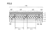
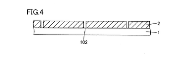
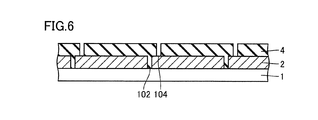
- FIG. FIG. 2 is a schematic cross-sectional view along II-II in FIG. It is typical sectional drawing illustrated about a part of manufacturing process of an example of the manufacturing method of the thin film solar cell module of embodiment. It is typical sectional drawing illustrating about another one part of the manufacturing process of an example of the manufacturing method of the thin film solar cell module of embodiment. It is typical sectional drawing illustrating about another one part of the manufacturing process of an example of the manufacturing method of the thin film solar cell module of embodiment. It is typical sectional drawing illustrating about another one part of the manufacturing process of an example of the manufacturing method of the thin film solar cell module of embodiment. It is typical sectional drawing illustrating about another one part of the manufacturing process of an example of the manufacturing method of the thin film solar cell module of embodiment.
- FIG. 6 is a schematic cross-sectional view of a thin film solar cell module according to Embodiment 2.
- FIG. It is a figure which shows the haze rate with respect to the light of wavelength 550nm of the surface transparent electrode layer which consists of a zinc oxide film
- FIG. It is a typical top view for illustrating the thin film photovoltaic cell arrange
- FIG. It is a figure which shows the relationship between the reflectance measured from the thickness of the white sealing material of the sample which laminated
- FIG. 6 is a schematic cross-sectional view of a thin film solar cell module according to Embodiment 3.
- FIG. FIG. 20 is a schematic cross-sectional view along XX-XX in FIG. 6 is a schematic cross-sectional view of a thin film solar cell module according to Embodiment 4.
- FIG. It is a figure which shows the haze rate with respect to the light of wavelength 550nm of the surface transparent electrode layer which consists of a zinc oxide film
- FIG. 1 It is a figure which shows the relationship between the thickness measured from the glass substrate side and the thickness of the white sealing material of the sample which laminated and hardened the white sealing material used in Example 2-1.
- FIG. It is a figure which shows the relationship between the haze rate in the surface of the surface transparent electrode layer of the thin film solar cell module of Comparative Example 2-1, and the short circuit current density of the bottom cell of a thin film solar cell.
- FIG. 1 shows a schematic cross-sectional view of the thin film solar cell module according to Embodiment 1.
- the thin-film solar cell module according to Embodiment 1 includes a translucent insulating substrate 1, an integrated cell string 110 provided on the translucent insulating substrate 1, and an integrated cell string 110.
- FIG. 2 shows a schematic cross-sectional view along II-II in FIG.
- the integrated cell string 110 is configured by connecting a plurality of thin-film solar cells 107 having the surface transparent electrode layer 2 in contact with the translucent insulating substrate 1 in series.
- the individual thin film photovoltaic cells 107 are formed on the surface transparent electrode layer 2 separated by the first separation groove 102 and the individual surface transparent electrode layer 2 separated by the first separation groove 102.
- the back transparent electrode layer 6 are laminated in this order.
- the back surface protective material 8 is not shown for convenience of explanation.
- the thin film semiconductor photoelectric conversion unit 4 is separated by the second separation groove 104, and the back surface transparent electrode layer 6 embedded in the second separation groove 104 is separated from the surface transparent electrode layer 2 of another adjacent thin film solar battery cell 107.
- adjacent thin-film solar cells 107 are sequentially connected in series.
- the individual thin-film solar cells 107 are separated by the third separation groove 106, and the insulating white sealing material 7 is embedded in the third separation groove 106.
- the thin film solar cell module of Embodiment 1 having the above structure, light such as sunlight is incident as incident light from the translucent insulating substrate 1 side, and is absorbed by the thin film semiconductor photoelectric conversion unit 4 to generate carriers. To do.
- the carriers generated in the thin film semiconductor photoelectric conversion unit 4 are taken out as current from the surface transparent electrode layer 2 on the front surface side and the back surface transparent electrode layer 6 on the back surface side.
- a bus bar (not shown) is formed on the back surface transparent electrode layer 6, and an output lead wire (not shown) is connected to the bus bar. Furthermore, the lead wire is taken out through the terminal box.
- the haze ratio of the surface transparent electrode layer 2 varies within the surface of the surface transparent electrode layer 2. And in the area
- the haze ratio varies within the surface of the surface transparent electrode layer of the thin film solar cell module, and the current density between the thin film solar cells in the integrated cell string varies depending on the height of the haze ratio. was found to occur. Since the current density of the integrated cell string is limited by the smallest current density of the thin film solar cells in the integrated cell string, it is preferable that the current densities of the thin film solar cells in the integrated cell string are as identical as possible.
- the ratio of the light incident from the translucent insulating substrate 1 side being scattered and / or refracted by the surface transparent electrode layer 2 is small. Since the distance (optical path length) passing through the unit 4 cannot be sufficiently increased, the ratio of transmission without being absorbed by the thin film semiconductor photoelectric conversion unit 4 is large.
- variation in the current density between the thin film solar cells 107 in the integrated cell string 110 can be reduced, the current density of the entire thin film solar cell module can be reduced. The decrease can be suppressed.
- the thickness of the white sealing material 7 disposed in the central region of the integrated cell string 110 is preferably smaller than the thickness of the white sealing material 7 disposed in the peripheral region of the integrated cell string 110. That is, since the haze ratio of the surface transparent electrode layer 2 is often lower in the peripheral region of the integrated cell string 110 than in the central region of the integrated cell string 110, the white color disposed in the peripheral region of the integrated cell string 110.
- the thickness of the sealing material 7 is preferably thicker than the thickness of the white sealing material 7 disposed in the central region of the integrated cell string 110.
- region where the haze rate of the surface transparent electrode layer 2 is high refers to the surface transparent electrode from the area
- region where the haze rate of the surface transparent electrode layer 2 is low refers to the surface of the surface transparent electrode layer 2 from the area
- the thickness of the white sealing material 7 means a thickness in a direction perpendicular to the surface on which the white sealing material 7 is provided.
- the minimum value of the haze ratio with respect to light having a wavelength of 550 nm in the effective cell area 111 of the surface transparent electrode layer 2 is preferably 6% or more.
- the surface transparent electrode layer 2 is less likely to be peeled off when the surface transparent electrode layer 2 has irregularities formed on the surface thereof to form a solar cell module. More light can reach the thin film semiconductor photoelectric conversion unit 4 by being scattered.
- the effective cell area 111 of the surface transparent electrode layer 2 means the area
- region which the thin film semiconductor photoelectric conversion unit 4 can generate electric power refers to the thin film semiconductor photoelectric conversion unit 4 from the area
- the surface transparent electrode layer 2 is located in a direction perpendicular to the surface.
- the surface transparent electrode layer 2 is formed on the translucent insulating substrate 1.
- the translucent insulating substrate 1 for example, a plate-like glass substrate having translucency and insulating properties, a resin substrate containing a transparent resin such as polyimide resin, or a substrate in which a plurality of these substrates are stacked is used. Can do.
- the surface transparent electrode layer 2 for example, a tin oxide film, an ITO (Indium Tin Oxide) film, a zinc oxide film, a single layer of a film obtained by adding a trace amount of impurities to these films, or a plurality of stacked layers thereof Layers and the like can be used. It is desirable that the surface transparent electrode layer 2 can transmit a large amount of light and has good conductivity.
- the surface transparent electrode layer 2 is composed of a plurality of layers, all the layers may be formed from the same material, or at least one layer may be formed from a material different from the others.
- the method for forming the surface transparent electrode layer 2 on the translucent insulating substrate 1 is not particularly limited, and for example, a CVD (Chemical Vapor Deposition) method or a sputtering method can be used.
- the surface of the surface transparent electrode layer 2 has irregularities as shown in FIG.
- irregularities on the surface of the surface transparent electrode layer 2 it is possible to increase the optical path length by scattering and / or refracting incident light incident from the translucent insulating substrate 1 side. Since the light confinement effect in 4 can be enhanced, the short-circuit current density can be increased.
- a wet etching method using dilute hydrochloric acid for example, a dry etching method represented by RIE (reactive ion etching) using argon gas or nitrogen gas, A method by mechanical processing such as sand blasting or a method using crystal growth of the surface transparent electrode layer 2 can be used.
- RIE reactive ion etching
- the haze ratio of the surface transparent electrode layer 2 may vary in-plane depending on the manufacturing conditions of the surface transparent electrode layer 2.
- the haze ratio of the surface transparent electrode layer 2 tends to vary in the plane of the surface transparent electrode layer 2. It is effective for.
- a first separation groove 102 for separating the surface transparent electrode layer 2 on the translucent insulating substrate 1 is formed.
- the formation method of the first separation groove 102 is not particularly limited, and for example, a method of removing a part of the surface transparent electrode layer 2 by a laser scribing method can be used.
- a laser beam used in the laser scribing method for forming the first separation groove 102 for example, a fundamental wave (wavelength 1064 nm) of a YAG (yttrium, aluminum, garnet) laser beam can be preferably used.
- a thin film semiconductor photoelectric conversion unit 4 is formed on the surface transparent electrode layer 2.
- the first separation groove 102 for separating the surface transparent electrode layer 2 is buried by the thin film semiconductor photoelectric conversion unit 4.
- the thin film semiconductor photoelectric conversion unit 4 for example, a laminated body in which an amorphous silicon photoelectric conversion unit and a microcrystalline silicon photoelectric conversion unit are stacked in this order from the translucent insulating substrate 1 side can be used.
- a first p-type semiconductor layer, a first i-type semiconductor layer, and a first n-type semiconductor layer are stacked in this order from the surface transparent electrode layer 2 side. It can comprise from the laminated body.
- the first p-type semiconductor layer examples include a p-type layer such as a p-type amorphous silicon layer, a p-type microcrystalline silicon layer, a p-type amorphous silicon carbide layer, or a p-type amorphous silicon nitride layer.
- a p-type layer such as a p-type amorphous silicon layer, a p-type microcrystalline silicon layer, a p-type amorphous silicon carbide layer, or a p-type amorphous silicon nitride layer.
- a single layer or a plurality of layers in which a plurality of these layers are stacked can be used.
- the first p-type semiconductor layer is composed of a plurality of layers, all the layers may be formed from the same semiconductor material, or at least one layer may be formed from a different semiconductor material.
- the p-type impurity element doped in the first p-type semiconductor layer for example, boron or the like can be
- the first i-type semiconductor layer for example, a single layer or a plurality of layers of amorphous silicon layers can be used.
- the first i-type semiconductor layer is an intrinsic semiconductor in which neither the p-type impurity element nor the n-type impurity element is doped.
- the first i-type semiconductor layer is close to the interface with the first p-type semiconductor layer and between the first n-type semiconductor layer and the first n-type semiconductor layer. In the vicinity of the interface, a small amount of p-type impurity element and n-type impurity element may be contained in the first i-type semiconductor layer.
- amorphous silicon carbide, amorphous silicon germanium, or the like to which elements such as carbon and germanium are positively added can be used.
- the first n-type semiconductor layer for example, an n-type amorphous silicon layer, a single n-type layer such as an n-type microcrystalline silicon layer, or a plurality of stacked layers of these layers can be used.
- the first n-type semiconductor layer is composed of a plurality of layers, all the layers may be formed from the same semiconductor material, or at least one layer may be formed from a different semiconductor material.
- the n-type impurity element doped in the first n-type semiconductor layer for example, phosphorus can be used.
- the same semiconductor material as that of the first i-type semiconductor layer may be used, or a different semiconductor material may be used.
- a p-type amorphous silicon layer and an i-type amorphous silicon layer are used for the first p-type semiconductor layer and the first i-type semiconductor layer, respectively, and an n-type microcrystal is used for the first n-type semiconductor layer.
- a silicon layer may be used.
- a p-type amorphous silicon carbide layer is used for the first p-type semiconductor layer
- an amorphous silicon layer is used for the first i-type semiconductor layer
- an n-type microscopic layer is used for the first n-type semiconductor layer.
- a crystalline silicon layer may be used.
- amorphous silicon is a concept including “hydrogenated amorphous silicon”
- microcrystalline silicon is a concept including “hydrogenated microcrystalline silicon”.
- the second p-type semiconductor layer, the second i-type semiconductor layer, and the second n-type semiconductor layer are stacked in this order from the amorphous silicon photoelectric conversion unit side. It can be comprised from a laminated body.
- the second p-type semiconductor layer for example, a single p-type layer such as a p-type microcrystalline silicon layer, a p-type microcrystalline silicon carbide layer, or a p-type microcrystalline silicon nitride layer, or a plurality of these layers are stacked. Multiple layers can be used. When the second p-type semiconductor layer is composed of a plurality of layers, all the layers may be formed from the same semiconductor material, or at least one layer may be formed from a different semiconductor material. . As the p-type impurity element doped in the second p-type semiconductor layer, for example, boron or the like can be used.
- the second i-type semiconductor layer for example, a single layer or a plurality of layers of a microcrystalline silicon layer can be used.
- the second i-type semiconductor layer is an intrinsic semiconductor layer in which neither the p-type impurity element nor the n-type impurity element is doped, but the vicinity of the interface with the second p-type semiconductor layer and the second n-type semiconductor layer In the vicinity of the interface, a p-type impurity element and an n-type impurity element may be contained in a trace amount in the second i-type semiconductor layer, respectively.
- the second n-type semiconductor layer for example, an n-type amorphous silicon layer, a single n-type layer such as an n-type microcrystalline silicon layer, or a plurality of stacked layers of these layers can be used.
- the second n-type semiconductor layer is composed of a plurality of layers, all the layers may be formed of the same semiconductor material, or at least one layer may be formed of a different semiconductor material.
- the n-type impurity element doped in the second n-type semiconductor layer for example, phosphorus or the like can be used.
- the same semiconductor material as that of the second i-type semiconductor layer may be used, or a different semiconductor material may be used.
- the second p-type semiconductor layer and the second n-type semiconductor layer may be made of the same semiconductor material or different semiconductor materials.
- the formation method of the thin film semiconductor photoelectric conversion unit 4 is not specifically limited, For example, plasma CVD method etc. can be used.
- a second separation groove 104 for separating the thin film semiconductor photoelectric conversion unit 4 is formed.
- the formation method of the second separation groove 104 is not particularly limited, and for example, a method of removing a part of the thin film semiconductor photoelectric conversion unit 4 by a laser scribing method can be used.
- a laser beam used in the laser scribing method for forming the second separation groove 104 for example, a second harmonic (wavelength of 532 nm) of YAG laser beam can be preferably used.
- the back transparent electrode layer 6 is formed on the thin film semiconductor photoelectric conversion unit 4.
- the second separation groove 104 for separating the thin film semiconductor photoelectric conversion unit 4 is filled with the back transparent electrode layer 6.
- the back transparent electrode layer 6 for example, a tin oxide film, an ITO film, a zinc oxide film, or a single layer of a film obtained by adding a trace amount of impurities to these films or a plurality of layers in which a plurality of these layers are stacked are allowed to transmit light.
- a conductive film can be used.
- all the layers may be made of the same material, or at least one layer may be made of a material different from the others.
- a third separation groove 106 for separating the thin film semiconductor photoelectric conversion unit 4 and the back transparent electrode layer 6 is formed.
- the integrated cell string 110 in which the adjacent thin film solar cells 107 are connected in series on the translucent insulating substrate 1 is formed.
- the formation method of the third separation groove 106 is not particularly limited, and for example, a method of removing a part of each of the thin film semiconductor photoelectric conversion unit 4 and the back surface transparent electrode layer 6 by a laser scribing method can be used.
- a method of removing a part of each of the thin film semiconductor photoelectric conversion unit 4 and the back surface transparent electrode layer 6 by a laser scribing method can be used.
- the laser beam used in the laser scribing method for forming the third separation groove 106 for example, the second harmonic (wavelength 532 nm) of YAG laser beam can be preferably used.
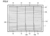
- a peripheral separation groove 108 that surrounds the peripheral edge of the integrated cell string 110 is formed, and a fourth separation groove that further separates the thin film solar cells 107 connected in series with each other. 109 is formed.
- the method for forming the peripheral separation groove 108 and the fourth separation groove 109 is not particularly limited.
- the surface transparent electrode layer 2, the thin film semiconductor photoelectric conversion unit 4, and the back surface transparent electrode layer 6 are formed by laser scribing or blasting. A method of removing a part of each can be used.
- a laser beam in the case of forming the peripheral separation groove 108 and the fourth separation groove 109 using a laser scribing method for example, a fundamental wave (wavelength 1064 nm) of YAG laser light can be preferably used.
- the bus bar electrodes 14 are attached to the back transparent electrode layers 6 of the thin film solar cells 107 at both ends of the integrated cell string 110 separated by the fourth separation grooves 109, respectively. Attach a lead wire (not shown) for taking out the output.
- the integrated cell string 110 is sealed between the translucent insulating substrate 1 and the white sealing material 7.
- the integrated cell string 110 can be sealed as follows, for example. First, as shown in FIG. 2, the white sealing material 7 is installed on the back surface transparent electrode layer 6, and then the back surface protection material 8 is installed on the white sealing material 7. Next, the translucent insulating substrate 1 after installation of the back surface protective material 8 is installed in a vacuum laminating apparatus, and pressurization and heating are performed while the back surface protective material 8 and the translucent insulating substrate 1 are deaerated. . Thereafter, the integrated cell string 110 can be sealed between the translucent insulating substrate 1 and the white sealing material 7 by cooling the white sealing material 7.
- the back surface protection material 8 a glass substrate, a PET resin film, a fluororesin film, etc. can be used, for example.
- the thickness of the white sealing material 7 after sealing becomes thin in the region corresponding to the region where the haze ratio of the surface transparent electrode layer 2 is high, and the surface transparent electrode layer 2 It is carried out by increasing the thickness in a region where the haze ratio is low.
- the surface of the thin film solar cell 107 disposed in the central region of the integrated cell string 110 compared with the haze ratio of the surface transparent electrode layer 2 of the thin film solar cell 107 disposed in the peripheral region of the integrated cell string 110, the surface of the thin film solar cell 107 disposed in the central region of the integrated cell string 110
- the haze ratio of the transparent electrode layer 2 is high (that is, compared with the haze ratio of the surface transparent electrode layer 2 of the thin-film solar cell 107 disposed in the central area of the integrated cell string 110, the peripheral region of the integrated cell string 110
- the haze ratio of the surface transparent electrode layer 2 of the thin-film solar cell 107 arranged in the above is low
- the integrated cell string 110 can be sealed by a combined method.
- the white sealing material is applied to the thin film solar cells 107 in the peripheral region of the integrated cell string 110 so as to be thicker than the white sealing material 7 installed in the thin film solar cells 107 in the central region of the integrated cell string 110. 7 is installed, and the integrated cell string 110 is sealed.
- the integrated cell string 110 is sealed by heating so that the heating temperature during lamination is lower.
- the white sealing material 7 an insulating material that is visually white or substantially white can be used.
- EVA ethylene vinyl acetate
- PVB polyvinyl butyral
- ionomer resin or an equivalent thereof
- the white sealing material 7 it is preferable to use PVB or ionomer resin to which dielectric fine particles such as titanium oxide and / or zinc oxide are added.
- PVB for example, “TROSIFOL® SOLAR PVB film R40” manufactured by Kuraray Co., Ltd., “DuponTM PV5200 Series” manufactured by Dupon, etc. can be cited.
- the white sealing material 7 can also serve as a sealing material that can seal the integrated cell string 110, but a sealing material different from the white sealing material 7 is installed on the white sealing material 7. Then, the integrated cell string 110 may be sealed.
- a sealing material for example, EVA and / or ionomer resin can be used.
- the output lead-out lead wire is taken out to the outside through the terminal box, and then the frame 9 made of, for example, aluminum is attached to the periphery of the translucent insulating substrate 1 so that the thin-film solar cell of the first embodiment Modules can be made.
- FIG. 10 shows a schematic cross-sectional view of the thin-film solar cell module of the second embodiment.
- the thin film solar cell module according to the second embodiment has the integrated cell string 110 and the white sealing material 7 installed between the translucent insulating substrate 1 and the back surface protective material 8 without using the frame 9. There is a feature.
- the surface transparent electrode layer 2 has a variation in haze ratio in the surface of the surface transparent electrode layer 2, and the thickness of the white sealing material 7 is the surface.
- the transparent electrode layer 2 is thin in a region corresponding to a region having a high haze ratio, and the surface transparent electrode layer 2 is thick in a region having a low haze ratio.
- the thin film solar cell module of the second embodiment since the variation in current density between the thin film solar cells 107 in the integrated cell string 110 can be reduced, the current density of the entire thin film solar cell module 1 is reduced. The decrease can be suppressed.
- Embodiment 2 since the description other than the above in Embodiment 2 is the same as that in Embodiment 1, the description thereof is omitted.
- FIG. 19 shows a schematic cross-sectional view of the thin-film solar cell module according to Embodiment 3.
- the thin-film solar cell module according to Embodiment 3 includes a translucent insulating substrate 1, an integrated cell string 110 provided on the translucent insulating substrate 1, and an integrated cell string 110.
- FIG. 20 shows a schematic cross-sectional view along XX-XX in FIG.
- the integrated cell string 110 is configured by connecting a plurality of thin-film solar cells 107 having the surface transparent electrode layer 2 in contact with the translucent insulating substrate 1 in series.
- the individual thin film photovoltaic cells 107 are formed on the surface transparent electrode layer 2 separated by the first separation groove 102 and the individual surface transparent electrode layer 2 separated by the first separation groove 102.
- the back transparent electrode layer 6 are laminated in this order.
- the back surface protective material 8 is not shown for convenience of explanation.
- the thin film semiconductor photoelectric conversion unit 4 is separated by the second separation groove 104, and the back surface transparent electrode layer 6 embedded in the second separation groove 104 is separated from the surface transparent electrode layer 2 of another adjacent thin film solar battery cell 107.
- adjacent thin-film solar cells 107 are sequentially connected in series.
- the individual thin-film solar cells 107 are separated by the third separation groove 106, and the insulating white sealing material 7 is embedded in the third separation groove 106.
- the thin film solar cell module of Embodiment 3 having the above structure, light such as sunlight is incident as incident light from the translucent insulating substrate 1 side, and is absorbed by the thin film semiconductor photoelectric conversion unit 4 to generate carriers. To do.
- the carriers generated in the thin film semiconductor photoelectric conversion unit 4 are taken out as current from the surface transparent electrode layer 2 on the front surface side and the back surface transparent electrode layer 6 on the back surface side.
- a bus bar (not shown) is formed on the back surface transparent electrode layer 6, and an output lead wire (not shown) is connected to the bus bar. Furthermore, the lead wire is taken out through the terminal box.
- the thickness of the white sealing material 7 in the peripheral region of the integrated cell string 110 is thinner than the thickness of the white sealing material 7 in the central region of the integrated cell string 110. Yes.
- the thin film solar cell 107 disposed in the peripheral region is more than the thin film solar cell 107 disposed in the central region of the integrated cell string 110 of the thin film solar cell module. It is easy to peel off, and the white sealing material 7 in the peripheral region of the integrated cell string 110 is disposed in such a peripheral region by making the thickness of the white sealing material 7 thinner than the thickness of the white sealing material 7 in the central region of the integrated cell string 110. This is because it has been found that peeling of the thin film solar cell 107 can be suppressed.
- the peeling suppression effect is maximized.
- the current density between the thin-film solar cells in the integrated cell string varies due to the haze ratio. Since the current density of the integrated cell string 110 is limited by the smallest current density of the thin film solar cell 107 in the integrated cell string 110, the current density of the thin film solar cell 107 in the integrated cell string 110 is as identical as possible. It is preferable.
- the variation in the current density of the thin film solar cells 107 in the integrated cell string 110 can be reduced, and the decrease in the current density of the entire thin film solar cell module can be suppressed. it can.
- the ratio of the light incident from the translucent insulating substrate 1 side being scattered and / or refracted by the surface transparent electrode layer 2 is small. Since the distance (optical path length) passing through the thin film semiconductor photoelectric conversion unit 4 cannot be sufficiently increased, the ratio of transmission without being absorbed by the thin film semiconductor photoelectric conversion unit 4 is large. Therefore, in the area
- the reflectance of the light transmitted to the white sealing material 7 side to the thin film semiconductor photoelectric conversion unit 4 side increases.
- region increases, and the current density of the thin film photovoltaic cell 107 arrange
- region increases.
- region where the haze rate of the surface transparent electrode layer 2 is low refers to the surface transparent electrode layer 2 from the center area
- vertical direction with respect to the surface of this is meant.
- region where the haze rate of the surface transparent electrode layer 2 is high is with respect to the surface of the surface transparent electrode layer 2 from the peripheral area
- the thickness of the white sealing material 7 means a thickness in a direction perpendicular to the surface on which the white sealing material 7 is provided.
- the minimum value of the haze ratio with respect to light having a wavelength of 550 nm of the surface transparent electrode layer 2 corresponding to the central region of the integrated cell string 110 is 6% or more.
- the surface transparent electrode layer 2 is less likely to be peeled off when the surface transparent electrode layer 2 has irregularities formed on the surface thereof to form a solar cell module. More light can reach the thin film semiconductor photoelectric conversion unit 4 by being scattered.
- the surface transparent electrode layer 2 is formed on the translucent insulating substrate 1.
- irregularities as shown in FIG. 19 are formed on the surface of the surface transparent electrode layer 2.
- irregularities on the surface of the surface transparent electrode layer 2 it is possible to increase the optical path length by scattering and / or refracting incident light incident from the translucent insulating substrate 1 side. Since the light confinement effect in 4 can be enhanced, the short-circuit current density can be increased.
- a method of forming irregularities on the surface of the surface transparent electrode layer 2 for example, a method by machining such as an etching method or sand blasting, or a method using crystal growth of the surface transparent electrode layer 2 can be used.
- the haze ratio of the surface transparent electrode layer 2 may be high in the peripheral region and low in the central region depending on the manufacturing conditions of the surface transparent electrode layer 2. it can.
- a method for increasing the haze ratio in the plane of the surface transparent electrode layer 2 in the peripheral region and decreasing it in the center region for example, dry etching of the surface of the surface transparent electrode layer 2 can be cited.
- a zinc oxide film having a haze ratio larger than a desired haze ratio is formed on the light-transmitting insulating substrate 1 as the surface transparent electrode layer 2 and, for example, argon gas or nitrogen gas is applied to an RIE (reactive ion etching) apparatus. After the introduction, dry etching of the surface of the surface transparent electrode layer 2 is performed.
- a desired haze rate variation is formed in the surface of the surface transparent electrode layer 2 by decreasing the etching rate in the peripheral region having a high haze rate and increasing the etching rate in the central region having a low haze rate. Can do.
- the plasma discharge density is made smaller than in the central region having a low haze ratio, or in the peripheral region having a high haze ratio, compared with the central region having a low haze ratio.
- the surface transparent electrode layer 2 has such a variation that the haze ratio is high in the peripheral region and low in the central region in the surface of the surface transparent electrode layer 2, for example, the surface transparent electrode layer The surface of 2 may be treated as described above to form a variation in haze ratio.
- a first separation groove 102 for separating the surface transparent electrode layer 2 on the translucent insulating substrate 1 is formed.
- a thin film semiconductor photoelectric conversion unit 4 is formed on the surface transparent electrode layer 2.
- the first separation groove 102 for separating the surface transparent electrode layer 2 is buried by the thin film semiconductor photoelectric conversion unit 4.
- a second separation groove 104 for separating the thin film semiconductor photoelectric conversion unit 4 is formed.
- a back transparent electrode layer 6 is formed on the thin film semiconductor photoelectric conversion unit 4.
- the second separation groove 104 for separating the thin film semiconductor photoelectric conversion unit 4 is filled with the back transparent electrode layer 6.
- a third separation groove 106 for separating the thin film semiconductor photoelectric conversion unit 4 and the back transparent electrode layer 6 is formed. Thereby, while being separated into the individual thin film solar cells 107, the integrated cell string 110 in which the adjacent thin film solar cells 107 are connected in series on the translucent insulating substrate 1 is formed.
- a peripheral separation groove 108 that surrounds the peripheral edge of the integrated cell string 110 is formed, and a fourth separation groove 109 that further separates the thin film solar cells 107 connected in series is formed.
- the method for forming the peripheral separation groove 108 and the fourth separation groove 109 is not particularly limited.
- the surface transparent electrode layer 2, the thin film semiconductor photoelectric conversion unit 4, and the back surface transparent electrode layer 6 are formed by laser scribing or blasting. A method of removing a part of each can be used.
- a laser beam in the case of forming the peripheral separation groove 108 and the fourth separation groove 109 using a laser scribing method for example, a fundamental wave (wavelength 1064 nm) of YAG laser light can be preferably used.
- the bus bar electrodes 14 are attached to the back transparent electrode layers 6 of the thin film solar cells 107 at both ends of the integrated cell string 110 separated by the fourth separation grooves 109, respectively. Attach a lead wire (not shown) for taking out the output.
- the integrated cell string 110 is sealed between the translucent insulating substrate 1 and the white sealing material 7.
- the integrated cell string 110 can be sealed as follows, for example. First, as shown in FIG. 20, the white sealing material 7 is installed on the back surface transparent electrode layer 6, and then the back surface protection material 8 is installed on the white sealing material 7. Next, the translucent insulating substrate 1 after installation of the back surface protective material 8 is installed in a vacuum laminating apparatus, and pressurization and heating are performed while the back surface protective material 8 and the translucent insulating substrate 1 are deaerated. . Thereafter, the integrated cell string 110 can be sealed between the translucent insulating substrate 1 and the white sealing material 7 by cooling the white sealing material 7.
- the back surface protection material 8 a glass substrate, a PET resin film, a fluororesin film, etc. can be used, for example.
- the sealing of the integrated cell string 110 is performed such that the thickness of the white sealing material 7 in the peripheral region of the integrated cell string 110 is thinner than the thickness of the white sealing material 7 in the central region of the integrated cell string 110. It is done. That is, the sealing of the integrated cell string 110 is performed so that the thickness of the white sealing material 7 in the central region of the integrated cell string 110 is larger than the thickness of the white sealing material 7 in the peripheral region of the integrated cell string 110. It is done.
- the integrated cell string 110 can be sealed by, for example, any one of the following methods (iii) and (iv), or a combination of (iii) and (iv).
- the white sealing material 7 is installed in the peripheral region of the integrated cell string 110 so as to be thinner than the white sealing material 7 installed in the central region of the integrated cell string 110, and the integrated cell string 110 is sealed. Stop.
- the white sealing material 7 installed in the peripheral region of the integrated cell string 110 has a higher heating temperature during lamination than the white sealing material 7 installed in the central region of the integrated cell string 110. And the integrated cell string 110 is sealed.
- the output lead-out lead wire is taken out through the terminal box, and then the frame 9 made of, for example, aluminum is attached to the periphery of the translucent insulating substrate 1 to thereby provide the thin-film solar cell of the third embodiment. Modules can be made.
- the thin film solar cell module using the conventional thin film solar cell there was a problem that the thin film solar cell located in the peripheral region was more easily peeled off than the thin film solar cell located in the central region.
- the surface transparent electrode layer 2 has a lower haze ratio than the thickness of the white sealing material 7 corresponding to the peripheral area where the haze ratio of the surface transparent electrode layer 2 is high. By increasing the thickness of the corresponding white sealing material 7, peeling of the thin-film solar battery cell located in the peripheral region can be suppressed.
- Embodiment 3 since the description other than the above in Embodiment 3 is the same as that in Embodiments 1 and 2, the description thereof is omitted.
- FIG. 21 is a schematic cross-sectional view of the thin film solar cell module according to Embodiment 4.
- the thin-film solar battery module according to Embodiment 4 has the integrated cell string 110 and the white sealing material 7 installed between the translucent insulating substrate 1 and the back surface protective material 8 without using the frame 9. There is a feature.
- the thickness of the white sealing material 7 in the peripheral region of the integrated cell string 110 is thinner than the thickness of the white sealing material 7 in the central region of the integrated cell string 110. Yes. That is, the thickness of the white sealing material 7 in the central region of the integrated cell string 110 is thicker than the thickness of the white sealing material 7 in the peripheral region of the integrated cell string 110.
- the thickness of the white sealing material 7 corresponding to the central region where the haze ratio of the surface transparent electrode layer 2 is lower than the thickness of 7 is thicker.
- Embodiment 4 since the description other than the above in Embodiment 4 is the same as that in Embodiments 1 to 3, the description thereof is omitted.
- a translucent insulating substrate 1 having a rectangular surface with a long side length of 1300 mm ⁇ short side length of 1000 mm and made of a glass substrate made of alkali-free glass with a thickness of 3.2 mm.
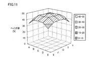
- the vertical axis in FIG. 11 indicates the haze ratio (%), A to E in FIG. 11 indicate 1000 mm on the short side, and E to Y in FIG. 11 indicate 1300 mm on the long side.
- the height of the haze rate is classified according to the type of diagonal lines.
- the surface transparent electrode layer 2 is partially removed by irradiating the surface transparent electrode layer 2 while linearly moving the fundamental wave (wavelength 1064 nm) of the YAG laser light.
- the first separation groove 102 for linearly separating the surface transparent electrode layer 2 was formed.
- a thin film semiconductor photoelectric conversion unit 4 was laminated on the surface transparent electrode layer 2.
- the thin film semiconductor photoelectric conversion unit 4 was produced as follows.
- the translucent insulating substrate 1 provided with the surface transparent electrode layer 2 having the above-described variation in haze ratio is placed in the film forming chamber of the plasma CVD apparatus, and the pressure inside the film forming chamber of the plasma CVD apparatus is set to 0.
- H 2 gas, SiH 4 gas, B 2 H 6 gas and CH 4 gas are introduced into the film formation chamber, and the surface of the zinc oxide film is formed by plasma CVD.
- a p-type amorphous silicon carbide layer was formed.
- the introduction of the gas into the film forming chamber is stopped, the gas in the film forming chamber is exhausted until the pressure inside the film forming chamber becomes 0.1 Pa, and then H 2 gas and SiH 4 are put into the film forming chamber.
- a gas was introduced to form a non-doped i-type amorphous silicon layer on the surface of the p-type amorphous silicon carbide layer by plasma CVD.
- the introduction of the gas into the film forming chamber is stopped, the gas in the film forming chamber is exhausted until the pressure inside the film forming chamber becomes 0.1 Pa, and then H 2 gas and SiH 4 gas are put into the film forming chamber.
- a PH 3 gas are introduced to form an n-type amorphous silicon layer on the surface of the non-doped i-type amorphous silicon layer by plasma CVD, and then a H 2 / SiH 4 flow rate ratio ((flow rate of H 2 ) / (Flow rate of SiH 4 )) is changed so that the flow rate of H 2 gas and the flow rate of SiH 4 gas are changed, and n-type microcrystals are formed on the surface of the n-type amorphous silicon layer by the plasma CVD method.
- a silicon layer was formed.
- a p-type amorphous silicon carbide layer, a non-doped i-type amorphous silicon layer, an n-type amorphous silicon layer, and an n-type microcrystalline silicon layer are stacked on the surface of the zinc oxide film.
- An amorphous silicon photoelectric conversion unit which is a top cell composed of a body was formed.
- the introduction of the gas into the film formation chamber is stopped, the gas in the film formation chamber is exhausted until the pressure inside the film formation chamber becomes 0.1 Pa, and then H 2 gas and SiH 4 are put into the film formation chamber.
- Gas and B 2 H 6 gas were introduced, and a p-type microcrystalline silicon layer was formed on the surface of the n-type microcrystalline silicon layer by plasma CVD.
- the introduction of the gas into the film forming chamber is stopped, the gas in the film forming chamber is exhausted until the pressure inside the film forming chamber becomes 0.1 Pa, and then the H 2 gas and the SiH 4 gas are put into the film forming chamber. Then, a non-doped i-type microcrystalline silicon layer was formed on the surface of the p-type microcrystalline silicon layer by plasma CVD.
- the introduction of the gas into the film forming chamber is stopped, the gas in the film forming chamber is exhausted until the pressure inside the film forming chamber becomes 0.1 Pa, and then H 2 gas and SiH 4 gas are put into the film forming chamber.
- a PH 3 gas are introduced to form an n-type amorphous silicon layer on the surface of the non-doped microcrystalline silicon layer by plasma CVD, and then a H 2 / SiH 4 flow rate ratio ((H 2 flow rate) / ( SiH 4 flow rate)) by changing the flow rate of the flow rate and the SiH 4 gas of H 2 gas as is high, forming an n-type microcrystalline silicon layer on the surface of the n-type amorphous silicon layer by a plasma CVD method did.
- a microcrystalline silicon photoelectric conversion unit which is a bottom cell made of a laminate of a p-type microcrystalline silicon layer, a non-doped i-type microcrystalline silicon layer, an n-type amorphous silicon layer and an n-type microcrystalline silicon layer produced as described above Formed.
- the top cell composed of the amorphous silicon photoelectric conversion unit and the microcrystalline silicon photoelectric layer.
- the translucent insulating substrate 1 after the formation of the thin film semiconductor photoelectric conversion unit 4 is taken out from the plasma CVD apparatus and installed in the magnetron sputtering apparatus, and the thin film semiconductor photoelectric conversion is performed by the magnetron sputtering method as shown in FIG.
- a back transparent electrode layer 6 made of a zinc oxide layer was formed on the surface of the unit 4.
- the thin film semiconductor photoelectric conversion unit 4 and the transparent back surface are irradiated by irradiating the back transparent electrode layer 6 while linearly moving the second harmonic (wavelength 532 nm) of the YAG laser light.
- a part of each electrode layer 6 was removed to form a third separation groove 106 that linearly separates the thin film semiconductor photoelectric conversion unit 4 and the back transparent electrode layer 6.
- an integrated cell string 110 was formed in which thin film solar cells 107 adjacent to each other on the translucent insulating substrate 1 were connected in series while being separated into the thin film solar cells 107.
- the back transparent electrode layer 6, the thin film semiconductor photoelectric conversion unit 4 and the surface are irradiated by irradiating the back transparent electrode layer 6 while moving the fundamental wave (wavelength 1064nm) of the YAG laser light.
- a part of each of the transparent electrode layers 2 is removed to form a peripheral separation groove 108 that surrounds the peripheral edge of the integrated cell string 110, and a fourth separation groove 109 that separates the thin film solar cells 107 connected in series with each other. Formed.
- the integrated cell string 110 has a configuration in which 90-stage thin film solar cells 107 are sequentially connected in series. In FIG. 9, not all of the 90-stage thin film solar cells 107 are shown for convenience of explanation.
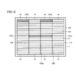
- the thin-film solar battery cell 107a disposed in the central region where the haze ratio of the surface transparent electrode layer 2 shown in FIG.
- the white sealing material 7 was installed so that it might become thick in the thin film photovoltaic cell 107b.
- white sealing material 7 “DuponTM PV5200 series” manufactured by Dupont was used.
- region is the 4th separation groove nearest to the center of the translucent insulated substrate 1 among the 4th separation grooves 109 which isolate
- the thin-film solar cell 107 b arranged in the peripheral region is a thin film solar battery cell arranged at a position closest to the peripheral edge of the translucent insulating substrate 1.
- FIG. 12 for convenience of explanation, only a part of each of the thin-film solar cells 107 a disposed in the central region and the thin-film solar cells 107 b disposed in the peripheral region is illustrated. Not all are shown.
- a sample was prepared by laminating the white sealing material 7 on a glass substrate and cured, and the relationship between the thickness of the white sealing material 7 of the sample and the reflectance measured from the glass substrate side was investigated. did.
- the result is shown in FIG.
- shaft of FIG. 13 has shown the reflectance (%) with respect to the light of wavelength 900nm
- shaft of FIG. 13 has shown the thickness (mm) of the white sealing material 7.
- FIG. 14 when the thickness of the white sealing material 7 of the above sample is 0.734 mm, 0.338 m, and 0.288 mm, respectively, and the white sealing material 7 is irradiated with light while changing the wavelength in various ways.
- the reflectance is shown.
- the vertical axis in FIG. 14 indicates the reflectance (%), and the horizontal axis in FIG. 14 indicates the wavelength (nm) of the light irradiated on the white sealing material 7.
- the solid line, broken line, and alternate long and short dash line in FIG. 14 indicate changes in the reflectance of the white sealing material 7 having thicknesses of 0.734 mm, 0.338 m, and 0.288 mm, respectively.
- a back surface protective material 8 made of a non-alkali glass glass substrate is installed on the white sealing material 7, and the translucent insulating substrate 1 after the back surface protective material 8 is installed is installed in a vacuum laminating apparatus. did. And by pressurizing and heating while deaerating between the translucent insulating substrate 1 and the back surface protective material 8, the white sealing material 7 between the translucent insulating substrate 1 and the back surface protective material 8 is used. The thin film semiconductor photoelectric conversion unit 4 was sealed.
- Example 2 For comparison, the same results as in Example 1 were obtained except that the thickness of the white sealing material 7 was made uniform regardless of variations in the in-plane haze ratio of the surface transparent electrode layer 2. A thin film solar cell module was produced.
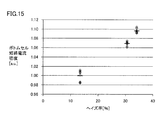
- the horizontal line of FIG. 15 shows the average value of the short circuit current density of the bottom cell of the thin film photovoltaic cell 107 arrange
- the vertical axis in FIG. 15 represents the average value of the short-circuit current density of the bottom cell of the thin-film solar cell 107 disposed at a position where the in-plane haze ratio of the surface transparent electrode layer 2 corresponds to 13.5%.
- the relative value of the short-circuit current density of the bottom cell is shown, and the horizontal axis of FIG. 15 shows the in-plane haze ratio of the surface transparent electrode layer 2.
- the thickness of the white sealing material 7 of the thin-film solar cell module of Comparative Example 1 is uniformly set to 0.288 mm, 0.338 mm, and 0.734 mm, respectively, and a solar simulator is used from the translucent insulating substrate 1 side.
- the short-circuit current density of the top cell and the short-circuit current density of the bottom cell of the specific thin-film solar battery 107 when irradiated with simulated sunlight (AM1.5, energy density 100 mW / cm 2 ) were measured. The result is shown in FIG.
- the diamond mark indicates the short-circuit current density of the top cell
- the square mark indicates the short-circuit current density of the bottom cell.
- the vertical axis of FIG. 16 represents the relative value of the short-circuit current density of the top cell and the bottom cell when the short-circuit current density of the top cell and the bottom cell is 1 when the thickness of the white sealing material 7 is 0.288 mm. Is shown. Further, the horizontal axis of FIG. 16 indicates the thickness of the white sealing material 7.
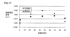
- rhombus marks indicate the short-circuit current density of each thin film solar battery cell 107 of the thin film solar battery module of Comparative Example 1
- square marks indicate each thin film solar battery cell of the thin film solar battery module of Example 1.
- a short-circuit current density of 107 is shown.
- the vertical axis in FIG. 17 represents the relative short-circuit current density of each thin-film solar cell 107 when the short-circuit current density of the first-stage thin-film solar cell 107 of the thin-film solar cell module of Comparative Example 1 is 1. The value is shown.
- the horizontal axis of FIG. 17 indicates the number of stages of the thin-film solar battery 107 in which the short-circuit current density is measured.
- the thickness of the white sealing material 7 can be made thinner than that in the region having a low haze ratio.
- a translucent insulating substrate 1 having a rectangular surface with a long side length of 1300 mm ⁇ short side length of 1000 mm and made of a glass substrate made of alkali-free glass with a thickness of 3.2 mm.
- the surface of the surface transparent electrode layer 2 is dry-etched so that the haze ratio of the peripheral region in the surface of the surface transparent electrode layer 2 made of the zinc oxide film is higher than the haze ratio of the central region, thereby making the surface transparent Unevenness was formed on the surface of the electrode layer 2.
- the vertical axis in FIG. 22 indicates the haze ratio (%), A to E in FIG. 22 indicate 1000 mm on the short side, and E to Y in FIG. 22 indicate 1300 mm on the long side.
- the height of the haze rate is classified according to the type of hatching.
- the surface transparent electrode layer 2 is partially removed by irradiating the surface transparent electrode layer 2 while linearly moving the fundamental wave (wavelength 1064 nm) of the YAG laser light.
- the first separation groove 102 for linearly separating the surface transparent electrode layer 2 was formed.
- a thin film semiconductor photoelectric conversion unit 4 was laminated on the surface transparent electrode layer 2.
- the thin film semiconductor photoelectric conversion unit 4 was produced as follows.
- the translucent insulating substrate 1 provided with the surface transparent electrode layer 2 having the above-described variation in haze ratio is placed in the film forming chamber of the plasma CVD apparatus, and the pressure inside the film forming chamber of the plasma CVD apparatus is set to 0.
- H 2 gas, SiH 4 gas, B 2 H 6 gas and CH 4 gas are introduced into the film formation chamber, and the surface of the zinc oxide film is formed by plasma CVD.
- a p-type amorphous silicon carbide layer was formed.
- the introduction of the gas into the film forming chamber is stopped, the gas in the film forming chamber is exhausted until the pressure inside the film forming chamber becomes 0.1 Pa, and then H 2 gas and SiH 4 are put into the film forming chamber.
- a gas was introduced to form a non-doped i-type amorphous silicon layer on the surface of the p-type amorphous silicon carbide layer by plasma CVD.
- the introduction of the gas into the film forming chamber is stopped, the gas in the film forming chamber is exhausted until the pressure inside the film forming chamber becomes 0.1 Pa, and then H 2 gas and SiH 4 gas are put into the film forming chamber.
- a PH 3 gas are introduced to form an n-type amorphous silicon layer on the surface of the non-doped i-type amorphous silicon layer by plasma CVD, and then a H 2 / SiH 4 flow rate ratio ((flow rate of H 2 ) / (Flow rate of SiH 4 )) is changed so that the flow rate of H 2 gas and the flow rate of SiH 4 gas are changed, and n-type microcrystals are formed on the surface of the n-type amorphous silicon layer by the plasma CVD method.
- a silicon layer was formed.
- a p-type amorphous silicon carbide layer, a non-doped i-type amorphous silicon layer, an n-type amorphous silicon layer, and an n-type microcrystalline silicon layer are stacked on the surface of the zinc oxide film.
- An amorphous silicon photoelectric conversion unit which is a top cell composed of a body was formed.
- the introduction of the gas into the film formation chamber is stopped, the gas in the film formation chamber is exhausted until the pressure inside the film formation chamber becomes 0.1 Pa, and then H 2 gas and SiH 4 are put into the film formation chamber.
- Gas and B 2 H 6 gas were introduced, and a p-type microcrystalline silicon layer was formed on the surface of the n-type microcrystalline silicon layer by plasma CVD.
- the introduction of the gas into the film forming chamber is stopped, the gas in the film forming chamber is exhausted until the pressure inside the film forming chamber becomes 0.1 Pa, and then the H 2 gas and the SiH 4 gas are put into the film forming chamber. Then, a non-doped i-type microcrystalline silicon layer was formed on the surface of the p-type microcrystalline silicon layer by plasma CVD.
- the introduction of the gas into the film forming chamber is stopped, the gas in the film forming chamber is exhausted until the pressure inside the film forming chamber becomes 0.1 Pa, and then H 2 gas and SiH 4 gas are put into the film forming chamber.
- a PH 3 gas are introduced to form an n-type amorphous silicon layer on the surface of the non-doped microcrystalline silicon layer by plasma CVD, and then a H 2 / SiH 4 flow rate ratio ((H 2 flow rate) / ( SiH 4 flow rate)) by changing the flow rate of the flow rate and the SiH 4 gas of H 2 gas as is high, forming an n-type microcrystalline silicon layer on the surface of the n-type amorphous silicon layer by a plasma CVD method did.
- a microcrystalline silicon photoelectric conversion unit which is a bottom cell made of a laminate of a p-type microcrystalline silicon layer, a non-doped i-type microcrystalline silicon layer, an n-type amorphous silicon layer and an n-type microcrystalline silicon layer produced as described above Formed.
- the top cell composed of the amorphous silicon photoelectric conversion unit and the bottom cell composed of the microcrystalline silicon photoelectric conversion unit are formed on the surface transparent electrode layer 2 having the variation in the haze ratio from the surface transparent electrode layer 2 side.
- the thin film semiconductor photoelectric conversion unit 4 laminated in order was formed.
- the translucent insulating substrate 1 after the formation of the thin film semiconductor photoelectric conversion unit 4 is taken out from the plasma CVD apparatus and installed in the magnetron sputtering apparatus, and the thin film semiconductor photoelectric conversion is performed by the magnetron sputtering method as shown in FIG.
- a back transparent electrode layer 6 made of a zinc oxide layer was formed on the surface of the unit 4.
- the thin film semiconductor photoelectric conversion unit 4 and the transparent back surface are irradiated by irradiating the back transparent electrode layer 6 while linearly moving the second harmonic (wavelength 532 nm) of the YAG laser light.
- a part of each electrode layer 6 was removed to form a third separation groove 106 that linearly separates the thin film semiconductor photoelectric conversion unit 4 and the back transparent electrode layer 6.
- an integrated cell string 110 was formed in which thin film solar cells 107 adjacent to each other on the translucent insulating substrate 1 were connected in series while being separated into the thin film solar cells 107.
- the back transparent electrode layer 6, the thin film semiconductor photoelectric conversion unit 4 and the surface are irradiated by irradiating the back transparent electrode layer 6 while moving the fundamental wave (wavelength 1064nm) of the YAG laser light.
- a part of each of the transparent electrode layers 2 is removed to form a peripheral separation groove 108 that surrounds the peripheral edge of the integrated cell string 110, and a fourth separation groove 109 that separates the thin film solar cells 107 connected in series with each other. Formed.
- the integrated cell string 110 has a configuration in which 90-stage thin film solar cells 107 are sequentially connected in series. In FIG. 9, not all of the 90-stage thin film solar cells 107 are shown for convenience of explanation.
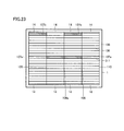
- the white sealing material 7 was installed so as to be thick in the thin film solar cell 107a arranged in the central region shown in FIG. 23 and thin in the thin film solar cell 107b arranged in the peripheral region.
- the white sealing material 7 “DuponTM PV5200 series” manufactured by Dupont was used.
- region is the 4th separation groove nearest to the center of the translucent insulated substrate 1 among the 4th separation grooves 109 which isolate
- the thin film solar battery cell 107 b arranged in the peripheral region is a thin film solar battery cell arranged at a position closest to the peripheral edge of the translucent insulating substrate 1.
- FIG. 23 for convenience of explanation, only a part of each of the thin-film solar cell 107a disposed in the central region and the thin-film solar cell 107b disposed in the peripheral region is illustrated. Not all are shown.
- a sample was prepared by laminating the white sealing material 7 on a glass substrate and cured, and the relationship between the thickness of the white sealing material 7 of the sample and the reflectance measured from the glass substrate side was investigated. did.
- the result is shown in FIG. Note that the vertical axis in FIG. 24 indicates the reflectance (%) with respect to light having a wavelength of 900 nm, and the horizontal axis in FIG. 24 indicates the thickness (mm) of the white sealing material 7.
- the reflectance increases as the thickness of the white sealing material 7 increases, and it was confirmed that the reflectance was 98% when the thickness of the white sealing material 7 was 1 mm. .
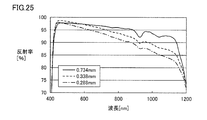
- FIG. 25 when the thickness of the white sealing material 7 of the above sample is 0.734 mm, 0.338 m, and 0.288 mm, respectively, and the white sealing material 7 is irradiated with light while changing the wavelength variously.
- the reflectance is shown.
- the vertical axis in FIG. 25 indicates the reflectance (%), and the horizontal axis in FIG. 25 indicates the wavelength (nm) of the light irradiated on the white sealing material 7.
- a solid line, a broken line, and a one-dot chain line in FIG. 25 indicate changes in reflectance of the white sealing material 7 having thicknesses of 0.734 mm, 0.338 m, and 0.288 mm, respectively.
- the reflectance of the white sealing material increases as the thickness of the white sealing material increases with respect to light in the wavelength range of 600 nm to 1200 nm.
- a back surface protective material 8 made of a PET resin film was placed on the white sealing material 7, and the translucent insulating substrate 1 after the back surface protective material 8 was placed was placed in a vacuum laminator. And by pressurizing and heating while deaerating between the translucent insulating substrate 1 and the back surface protective material 8, the white sealing material 7 between the translucent insulating substrate 1 and the back surface protective material 8 is used. The thin film semiconductor photoelectric conversion unit 4 was sealed.
- the lead wire for taking out the output is taken out to the outside through the terminal box, and then the frame 9 made of, for example, aluminum is attached to the periphery of the translucent insulating substrate 1 as shown in FIG. A thin film solar cell module 2-1 was produced.
- Example 2-2 A thin-film solar cell module of Example 2-2 was produced in the same manner as in Example 2-1, except that the frame 9 was not attached and a glass substrate was used as the back surface protective material 8.
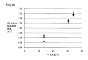
- Comparative Example 2-1 For comparison, a thin film solar cell module of Comparative Example 2-1 was produced in the same manner as in Example 2-1, except that the thickness of the white sealing material 7 was made uniform.
- the horizontal line of FIG. 26 shows the average value of the short circuit current density of the bottom cell of the thin film photovoltaic cell 107 arrange
- the vertical axis of FIG. 26 indicates that the average value of the short-circuit current density of the bottom cell of the thin-film solar cell 107 disposed at a position where the in-plane haze ratio of the surface transparent electrode layer 2 corresponds to 13.5% is 1.
- the relative value of the short-circuit current density of the bottom cell is shown, and the horizontal axis of FIG. 26 shows the in-plane haze ratio of the surface transparent electrode layer 2.
- the thickness of the white sealing material 7 of the thin-film solar cell module of Comparative Example 2-1 was uniformly set to 0.288 mm, 0.338 mm, and 0.734 mm, respectively, and a solar simulator was applied from the translucent insulating substrate 1 side.
- the short-circuit current density of the top cell and the short-circuit current of the specific thin-film solar cell 107 when irradiated with simulated sunlight (AM1.5, energy density 100 mW / cm 2 ) were measured. The result is shown in FIG.
- the diamond marks indicate the short-circuit current density of the top cell
- the square marks indicate the short-circuit current density of the bottom cell.
- the vertical axis of FIG. 27 represents the relative value of the short-circuit current density of the top cell and the bottom cell when the short-circuit current density of the top cell and the bottom cell is 1 when the thickness of the white sealing material 7 is 0.288 mm. Is shown.
- the horizontal axis in FIG. 27 indicates the thickness of the white sealing material 7.
- Comparative Example 2-2 A thin film solar cell module of Comparative Example 2-2 was produced in the same manner as Comparative Example 2-1, except that the frame 9 was not attached and a glass substrate was used as the back surface protective material 8.
- Table 1 shows the high-temperature and high-humidity test of the thin-film solar cells arranged in the peripheral region of each thin-film solar cell module of Example 2-1, Example 2-2, Comparative Example 2-1 and Comparative Example 2-2.
- Table 2 shows the presence or absence of previous peeling, and Table 2 shows the thin films disposed in the peripheral regions of the thin film solar cell modules of Example 2-1, Example 2-2, Comparative Example 2-1, and Comparative Example 2-2. The presence or absence of peeling after the high temperature and high humidity test of a photovoltaic cell is shown.
- the presence or absence of peeling of the thin-film solar battery cell is at least of a plurality of peripheral regions of the thin-film solar battery modules of Example 2-1, Example 2-2, Comparative Example 2-1, and Comparative Example 2-2.
- film peeling of 10 mm or more was observed in one peripheral area, it was judged that there was peeling.
- Table 1 and Table 2 the presence or absence of peeling is shown in percentage (%).
- the high temperature and high humidity test was carried out in a test tank having a test temperature of 85 ° C. ⁇ 2 ° C. and a relative humidity of (85 ⁇ 5)% based on “JIS C8991: 2011 10.13 High temperature and high humidity test”.
- 2-1, Example 2-2, Comparative Example 2-1 and Comparative Example 2-2 were each left for 1000 hours, and the presence or absence of peeling of the thin film solar cell before and after the high temperature and high humidity test was visually observed. This was done by checking.
- the thin film solar cell modules of Example 2-1 and Example 2-2 did not peel off the thin film solar cells arranged in the peripheral region.
- the thin film solar cell module of Comparative Example 2-1 the thin film solar cell was peeled in the peripheral region of 25%, and in the thin film solar cell module of Comparative Example 2-2, the peripheral region was 37.5%. It was seen.
- the thickness of the white sealing material in the peripheral region of the integrated cell string is made thinner than the thickness of the white sealing material in the central region of the integrated cell string, thereby thin film solar cells arranged in the peripheral region It was confirmed that the peeling of can be effectively suppressed.
- the diamond mark indicates the short-circuit current density of each thin film solar cell 107 of the thin film solar cell module of Comparative Example 2-1
- the square mark indicates each of the thin film solar cell modules of Example 2-1.
- the short circuit current density of the thin film photovoltaic cell 107 is shown.
- the vertical axis in FIG. 28 indicates the short-circuit current density of each thin-film solar cell 107 when the short-circuit current density of the 45th-stage thin-film solar cell 107 of the thin-film solar cell module of Comparative Example 2-1 is 1. The relative value of is shown.
- the horizontal axis of FIG. 28 indicates the number of stages of the thin-film solar battery 107 in which the short-circuit current density is measured.
- Example 2-1 the variation in the short circuit current density of each thin film solar cell 107 can be reduced as compared with the thin film solar cell module of Comparative Example 2-1. It was confirmed that Further, it was confirmed that the power generation efficiency of the integrated cell string 110 was improved by 0.33% in Example 2-1 compared to Comparative Example 2-1. These are considered to be because the current density of the thin-film solar cell 107 in the central region where the in-plane haze ratio of the surface transparent electrode layer 2 is low is increased by increasing the thickness of the white sealing material 7.
- the present invention can be used for a thin film solar cell module and a method for manufacturing a thin film solar cell module.
Landscapes
- Photovoltaic Devices (AREA)
Abstract
表面透明電極層(2)の面内のヘイズ率にばらつきがあり、表面透明電極層(2)のヘイズ率が低い領域に対応する白色封止材(7)の領域では白色封止材(7)の厚さが厚くなる薄膜太陽電池モジュールとその製造方法である。
Description
本発明は、薄膜太陽電池モジュールおよび薄膜太陽電池モジュールの製造方法に関する。
近年、クリーンエネルギー源として太陽電池モジュールが急速に普及しつつある。一般に、最も普及している太陽電池モジュールは、結晶シリコン太陽電池セルなどの結晶系の太陽電池セルを用いたものであるが、資源面での制約がより少なく、かつ発電コストの削減を見込めることから、近年、薄膜半導体を用いた薄膜系の薄膜太陽電池セルを用いた薄膜太陽電池モジュールの開発が盛んに行なわれている。
従来の薄膜太陽電池セルは、一般に、ガラスなどの透光性絶縁基板上に、順に積層された、表面透明電極層と、p型薄膜半導体層、i型薄膜半導体層およびn型薄膜半導体層で構成される1つ以上の薄膜半導体光電変換ユニットと、裏面電極層とを含んでいる。近年最も開発が行なわれている薄膜太陽電池セルは、シリコンを主成分とするものであり、非晶質シリコン系、結晶質シリコン系、および両者を積層して直列に重ねたタンデム系などが実用化されている。
上記の薄膜半導体光電変換ユニットの厚さの大部分は、実質的に真性の半導体層であるi型薄膜半導体層によって占められ、光電変換作用は主としてこのi型薄膜半導体層内で生じる。したがって、光電変換層であるi型薄膜半導体層の膜厚は、光吸収のためには厚い方が好ましいが、必要以上に厚くした場合には、その堆積のためのコストと時間とが増大することになる。
この問題を解決する方法として、たとえば特許文献1(特開2001-7361号公報)には、裏面電極層を酸化亜鉛(ZnO)などの裏面透明導電層と銀(Ag)などの高反射金属層との2層を用いて、薄膜半導体光電変換ユニットを透過した光を薄膜半導体光電変換ユニットに再入射させる方法、および入射光側の表面透明電極層や裏面電極層に凹凸を設けて光を拡散させ、光路長を長くすることによって吸収量を増加させる方法などが記載されている。
また、特許文献2(米国特許出願公開第2005/0172997号明細書)には、裏面電極層として、透明酸化物導電層と白色封止材からなる裏面反射層とを用いて発電効率の高い薄膜太陽電池モジュールが得られることが記載されている。
しかしながら、従来の薄膜太陽電池セルを用いた薄膜太陽電池モジュールにおいては、薄膜太陽電池セルの複数が直列に接続された集積セルストリング内の薄膜太陽電池セルの電流密度にばらつきが生じることがあった。
集積セルストリング内の薄膜太陽電池セルの電流密度にばらつきが生じた場合には、集積セルストリングの電流密度が薄膜太陽電池セルの最小の電流密度に律速されて、薄膜太陽電池モジュールの全体の電流密度が低下してしまうという問題があった。
上記の事情に鑑みて、本発明の目的は、薄膜太陽電池モジュール全体の電流密度の低下を抑制することが可能な薄膜太陽電池モジュールおよび薄膜太陽電池モジュールの製造方法を提供することにある。
本発明は、透光性絶縁基板と、透光性絶縁基板上に設けられた集積セルストリングと、集積セルストリング上に設けられた白色封止材と、を備え、集積セルストリングは、透光性絶縁基板に接する表面透明電極層を有する薄膜太陽電池セルの複数が直列接続されてなり、表面透明電極層は、表面透明電極層の面内において、ヘイズ率にばらつきを有しており、表面透明電極層のヘイズ率が低い領域に対応する白色封止材の領域では、白色封止材の厚さが厚くなる薄膜太陽電池モジュールである。
ここで、本発明の薄膜太陽電池モジュールにおいて、表面透明電極層のヘイズ率が低い領域に対応する白色封止材の領域は集積セルストリングの周縁領域に配置された白色封止材の領域であって、集積セルストリングの周縁領域に配置された白色封止材の領域では、集積セルストリングの中心領域に対応する白色封止材の領域よりも白色封止材の厚さが厚くなることが好ましい。
ここで、本発明の薄膜太陽電池モジュールにおいて、表面透明電極層の有効セルエリアにおける波長550nmの光に対するヘイズ率の最小値が6%以上であることが好ましい。
また、本発明の薄膜太陽電池モジュールにおいて、集積セルストリングの中心領域における表面透明電極層のヘイズ率が、集積セルストリングの周縁領域における表面透明電極層のヘイズ率よりも低く、集積セルストリングの中心領域における白色封止材の厚さが、集積セルストリングの周縁領域における白色封止材の厚さよりも厚いことが好ましい。
ここで、本発明の薄膜太陽電池モジュールにおいては、集積セルストリングの中心領域に対応する表面透明電極層の波長550nmの光に対するヘイズ率の最小値が6%以上であることが好ましい。
また、本発明の薄膜太陽電池モジュールにおいては、透光性絶縁基板の表面の面積は1m2以上であることが好ましい。
また、本発明は、透光性絶縁基板上に集積セルストリングを形成する工程と、透光性絶縁基板と白色封止材との間に集積セルストリングを封止する工程と、を含み、集積セルストリングは、透光性絶縁基板に接する表面透明電極層を有する薄膜太陽電池セルの複数が直列接続されてなり、表面透明電極層は、表面透明電極層の面内において、ヘイズ率にばらつきを有しており、集積セルストリングを封止する工程において、集積セルストリングは、白色封止材の厚さが、表面透明電極層のヘイズ率が低い領域に対応する白色封止材の領域で厚くなるように封止される、薄膜太陽電池モジュールの製造方法である。
ここで、本発明の薄膜太陽電池モジュールの製造方法においては、表面透明電極層のヘイズ率が低い領域に対応する白色封止材の領域は、集積セルストリングの周縁領域に配置された白色封止材の領域であって、集積セルストリングは、集積セルストリングの周縁領域に配置された白色封止材の領域では、集積セルストリングの中心領域に対応する白色封止材の領域よりも白色封止材の厚さが厚くなるように封止されることが好ましい。
また、本発明の薄膜太陽電池モジュールの製造方法においては、集積セルストリングの中心領域における表面透明電極層のヘイズ率が、集積セルストリングの周縁領域における表面透明電極層のヘイズ率よりも低く、集積セルストリングを封止する工程において、集積セルストリングは、集積セルストリングの中心領域における白色封止材の厚さが、集積セルストリングの周縁領域における白色封止材の厚さよりも厚くなるように封止される薄膜太陽電池モジュールの製造方法である。
本発明によれば、薄膜太陽電池モジュール全体の電流密度の低下を抑制することが可能な薄膜太陽電池モジュールおよび薄膜太陽電池モジュールの製造方法を提供することができる。
以下、本発明の実施の形態について説明する。なお、本発明の図面において、同一の参照符号は、同一部分または相当部分を表わすものとする。
<実施の形態1>
図1に、実施の形態1の薄膜太陽電池モジュールの模式的な断面図を示す。図1に示すように、実施の形態1の薄膜太陽電池モジュールは、透光性絶縁基板1と、透光性絶縁基板1上に設けられた集積セルストリング110と、集積セルストリング110上に設けられた白色封止材7と、白色封止材7上に設けられた裏面保護材8と、透光性絶縁基板1の周縁に取り付けられたフレーム9と、を備えている。
図1に、実施の形態1の薄膜太陽電池モジュールの模式的な断面図を示す。図1に示すように、実施の形態1の薄膜太陽電池モジュールは、透光性絶縁基板1と、透光性絶縁基板1上に設けられた集積セルストリング110と、集積セルストリング110上に設けられた白色封止材7と、白色封止材7上に設けられた裏面保護材8と、透光性絶縁基板1の周縁に取り付けられたフレーム9と、を備えている。
図2に、図1のII-IIに沿った模式的な断面図を示す。図2に示すように、集積セルストリング110は、透光性絶縁基板1に接する表面透明電極層2を有する薄膜太陽電池セル107の複数が直列接続されることによって構成されている。個々の薄膜太陽電池セル107は、第1分離溝102によって分離された表面透明電極層2と、第1分離溝102によって分離された個々の表面透明電極層2上に、薄膜半導体光電変換ユニット4と、裏面透明電極層6と、がこの順に積層された構造を有している。なお、図2においては、説明の便宜のため、裏面保護材8については図示していない。
薄膜半導体光電変換ユニット4は、第2分離溝104によって分離されており、第2分離溝104を埋め込んだ裏面透明電極層6が、隣り合う他の薄膜太陽電池セル107の表面透明電極層2と電気的に接続することによって、隣り合う薄膜太陽電池セル107同士が順次直列接続されている。
個々の薄膜太陽電池セル107は、第3分離溝106によって分離されており、第3分離溝106には、絶縁性の白色封止材7が埋め込まれている。
上記の構造を有する実施の形態1の薄膜太陽電池モジュールにおいては、透光性絶縁基板1側から太陽光などの光が入射光として入射し、薄膜半導体光電変換ユニット4で吸収されてキャリアが発生する。そして、薄膜半導体光電変換ユニット4で発生したキャリアは、表面側の表面透明電極層2と、裏面側の裏面透明電極層6とから、電流として取り出される。なお、裏面透明電極層6には、バスバー(図示せず)が形成されており、バスバーには出力取り出し用のリード線(図示せず)が接続されている。さらに、リード線は、端子ボックスを介して外部に取り出されている。
実施の形態1の薄膜太陽電池モジュールにおいては、表面透明電極層2のヘイズ率が、表面透明電極層2の面内において、ばらつきを有している。そして、表面透明電極層2のヘイズ率が低い領域に対応する白色封止材7の領域では白色封止材7の厚さを厚くしている。
なお、本明細書において、「ヘイズ率」とは、たとえば図18の模式図に示すように、透光性絶縁基板1および表面透明電極層2を透過してきた入射光21の全光線透過光(Tt)22中の拡散透過光(Td)23の割合で、ヘイズ率(%)=100×Td/Ttの式で表わされ、ヘイズ率が高いほど光の拡散する割合が高いことを意味する。
本発明者が鋭意検討した結果、薄膜太陽電池モジュールの表面透明電極層の面内においてヘイズ率がばらついており、ヘイズ率の高低によって、集積セルストリング内の薄膜太陽電池セル間の電流密度にばらつきが生じることが判明した。集積セルストリングの電流密度は、集積セルストリング内の薄膜太陽電池セルの最も小さい電流密度に律速されるため、集積セルストリング内の薄膜太陽電池セルの電流密度はなるべく同一であることが好ましい。
そして、実施の形態1の薄膜太陽電池モジュールのように、表面透明電極層2のヘイズ率が低い領域に対応する白色封止材7の領域では、表面透明電極層2のヘイズ率が高い領域に対応する白色封止材7と比べて、白色封止材7の厚さを厚くすることによって、集積セルストリング110内の薄膜太陽電池セル107の電流密度のばらつきを低減できることを見い出し、本発明を完成するに至った。その理由は以下のように考えられる。
すなわち、表面透明電極層2のヘイズ率が低い領域では、透光性絶縁基板1側から入射してきた光が表面透明電極層2で散乱および/または屈折される割合が小さいため、薄膜半導体光電変換ユニット4を通過する距離(光路長)を十分に伸ばすことができないことから、薄膜半導体光電変換ユニット4で吸収されることなく、透過してしまう割合が大きい。そのため、表面透明電極層2のヘイズ率が低い領域に対応する白色封止材7の領域では、表面透明電極層2のヘイズ率が高い領域に対応する白色封止材7の領域と比べて、白色封止材7の厚さを厚くすることによって、白色封止材7側に透過してきた光の薄膜半導体光電変換ユニット4側への反射率が上がる。これにより、薄膜半導体光電変換ユニット4に入射する光量が増大して、当該領域に配置された薄膜太陽電池セル107の電流密度が増大する。
これにより、実施の形態1の薄膜太陽電池モジュールにおいては、集積セルストリング110内の薄膜太陽電池セル107間の電流密度のばらつきを低減することができるために、薄膜太陽電池モジュール全体の電流密度の低下を抑制することができる。
一般的には、集積セルストリング110の中心領域は、集積セルストリング110の周縁領域と比べて、表面透明電極層2のヘイズ率が高くなることが多い。そのため、集積セルストリング110の中心領域に配置された白色封止材7の厚さは、集積セルストリング110の周縁領域に配置された白色封止材7の厚さよりも薄くなることが好ましい。すなわち、集積セルストリング110の周縁領域は、集積セルストリング110の中心領域と比べて、表面透明電極層2のヘイズ率が低くなることが多いため、集積セルストリング110の周縁領域に配置された白色封止材7の厚さは、集積セルストリング110の中心領域に配置された白色封止材7の厚さよりも厚くなることが好ましい。
なお、本明細書において、表面透明電極層2のヘイズ率が高い領域に対応する白色封止材7の領域とは、表面透明電極層2の面内のヘイズ率が高い領域から、表面透明電極層2の表面に対して、垂直方向に位置する白色封止材7の領域を意味する。また、表面透明電極層2のヘイズ率が低い領域に対応する白色封止材7の領域とは、表面透明電極層2の面内のヘイズ率が低い領域から、表面透明電極層2の表面に対して、垂直方向に位置する白色封止材7の領域を意味する。
また、本明細書において、白色封止材7の厚さは、白色封止材7が設けられている面に対して垂直方向の厚さを意味する。
また、表面透明電極層2の有効セルエリア111における波長550nmの光に対するヘイズ率の最小値は6%以上であることが好ましい。この場合には、表面透明電極層2の表面に凹凸を形成して太陽電池モジュールとしたときの表面透明電極層2の剥離が発生しにくくなり、表面透明電極層2の表面の凹凸で光を散乱させて、より多くの光を薄膜半導体光電変換ユニット4に到達させることができる。
また、図2に示すように、表面透明電極層2の有効セルエリア111は、薄膜太陽電池セル107の薄膜半導体光電変換ユニット4が発電可能な領域に対応する表面透明電極層2の領域を意味する。なお、本明細書において、薄膜半導体光電変換ユニット4が発電可能な領域に対応する表面透明電極層2の領域とは、薄膜半導体光電変換ユニット4の発電可能な領域から、薄膜半導体光電変換ユニット4の表面に対して、垂直方向に位置する表面透明電極層2の領域を意味する。
以下、図3~図9を参照して、実施の形態1の薄膜太陽電池モジュールの製造方法の一例について説明する。まず、図3の模式的断面図に示すように、透光性絶縁基板1上に表面透明電極層2を形成する。
透光性絶縁基板1としては、たとえば、透光性および絶縁性を有する板状のガラス基板、ポリイミド樹脂などの透明樹脂を含む樹脂基板、またはこれらの基板の複数を積層した基板などを用いることができる。また、表面透明電極層2としては、たとえば酸化錫膜、ITO(Indium Tin Oxide)膜、酸化亜鉛膜、若しくはこれらの膜に微量の不純物を添加した膜の単層またはこれらを複数重ね合わせた複数層などを用いることができる。表面透明電極層2は、光を多く透過させることができるとともに良好な導電性を有することが望ましい。表面透明電極層2が複数層から構成される場合には、すべての層が同一の材料から形成されていてもよく、少なくとも1層が他と異なる材料から形成されていてもよい。
透光性絶縁基板1上に表面透明電極層2を形成する方法は、特に限定されないが、たとえばCVD(Chemical Vapor Deposition)法またはスパッタ法などを用いることができる。
また、表面透明電極層2の表面にはたとえば図1に示すような凹凸が形成されていることが好ましい。表面透明電極層2の表面に凹凸が形成されていることによって、透光性絶縁基板1側から入射した入射光を散乱および/または屈折させて光路長を伸ばすことができ、薄膜半導体光電変換ユニット4における光閉じ込め効果を高めることができるため短絡電流密度を増大させることができる。表面透明電極層2の表面に凹凸を形成する方法としては、たとえば、希塩酸などを用いたウエットエッチング法、アルゴンガスや窒素ガスを用いたRIE(反応性イオンエッチング)に代表されるドライエッチング法、サンドブラストのような機械加工による方法、または表面透明電極層2の結晶成長を利用する方法などを用いることができる。
表面透明電極層2の表面に凹凸が形成されている場合には、表面透明電極層2のヘイズ率は、表面透明電極層2の製造条件によって、面内にばらつきを有することがある。特に透光性絶縁基板1の表面の面積が1m2以上である場合には、表面透明電極層2のヘイズ率が、表面透明電極層2の面内にばらつきを有する傾向が大きいため、本発明に有効である。
次に、図4の模式的断面図に示すように、透光性絶縁基板1上の表面透明電極層2を分離する第1分離溝102を形成する。
第1分離溝102の形成方法は、特に限定されないが、たとえばレーザスクライブ法により表面透明電極層2の一部を除去する方法などを用いることができる。第1分離溝102の形成のためのレーザスクライブ法に用いられるレーザ光としては、たとえばYAG(イットリウム・アルミニウム・ガーネット)レーザ光の基本波(波長1064nm)などを好適に用いることができる。
次に、図5の模式的断面図に示すように、表面透明電極層2上に薄膜半導体光電変換ユニット4を形成する。このとき、表面透明電極層2を分離する第1分離溝102が薄膜半導体光電変換ユニット4によって埋め込まれることになる。
薄膜半導体光電変換ユニット4としては、たとえば、透光性絶縁基板1側から、非晶質シリコン光電変換ユニットと、微結晶シリコン光電変換ユニットとをこの順に積層した積層体などを用いることができる。
非晶質シリコン光電変換ユニットは、たとえば、表面透明電極層2側から、第1のp型半導体層と、第1のi型半導体層と、第1のn型半導体層とがこの順に積層された積層体から構成することができる。
第1のp型半導体層としては、たとえば、p型非晶質シリコン層、p型微結晶シリコン層、p型非晶質炭化シリコン層、またはp型非晶質窒化シリコン層などのp型層の単層またはこれらを複数重ね合わせた複数層を用いることができる。第1のp型半導体層が複数層から構成される場合には、すべての層が同一の半導体材料から形成されていてもよく、少なくとも1層が他と異なる半導体材料から形成されていてもよい。第1のp型半導体層にドープされるp型不純物元素としては、たとえばボロンなどを用いることができる。
第1のi型半導体層としては、たとえば、非晶質シリコン層の単層または複数層などを用いることができる。第1のi型半導体層は、p型不純物元素およびn型不純物元素のいずれもドープされない真性半導体であるが、第1のp型半導体層との界面近傍および第1のn型半導体層との界面近傍ではそれぞれp型不純物元素およびn型不純物元素が第1のi型半導体層中に微量に含まれる場合がある。また、第1のi型半導体層のバンドギャップを制御するために、炭素、ゲルマニウム等の元素を積極的に添加した非晶質炭化シリコン、非晶質シリコンゲルマニウム等を用いることもできる。
第1のn型半導体層としては、たとえば、n型非晶質シリコン層、またはn型微結晶シリコン層などのn型層の単層またはこれらを複数重ね合わせた複数層などを用いることができる。第1のn型半導体層が複数層から構成される場合には、すべての層が同一の半導体材料から形成されていてもよく、少なくとも1層が他と異なる半導体材料から形成されていてもよい。第1のn型半導体層にドープされるn型不純物元素としては、たとえばリンなどを用いることができる。
なお、第1のp型半導体層および第1のn型半導体層としては、第1のi型半導体層と同一の半導体材料を用いてもよく、異なる半導体材料を用いてもよい。たとえば、第1のp型半導体層および第1のi型半導体層にそれぞれp型非晶質シリコン層およびi型非晶質シリコン層を用いるとともに、第1のn型半導体層にn型微結晶シリコン層を用いてもよい。また、たとえば、第1のp型半導体層にp型非晶質炭化シリコン層を用い、第1のi型半導体層に非晶質シリコン層を用い、第1のn型半導体層にn型微結晶シリコン層を用いてもよい。
また、本明細書において、「非晶質シリコン」は「水素化非晶質シリコン」を含む概念であり、「微結晶シリコン」は「水素化微結晶シリコン」を含む概念である。
微結晶シリコン光電変換ユニットは、非晶質シリコン光電変換ユニット側から、第2のp型半導体層と、第2のi型半導体層と、第2のn型半導体層とがこの順に積層された積層体から構成することができる。
第2のp型半導体層としては、たとえば、p型微結晶シリコン層、p型微結晶炭化シリコン層、またはp型微結晶窒化シリコン層などのp型層の単層またはこれらを複数重ね合わせた複数層を用いることができる。第2のp型半導体層が複数層から構成される場合には、すべての層が同一の半導体材料から形成されていてもよく、少なくとも1層が他と異なる半導体材料から形成されていてもよい。第2のp型半導体層にドープされるp型不純物元素としては、たとえばボロンなどを用いることができる。
第2のi型半導体層としては、たとえば、微結晶シリコン層の単層または複数層などを用いることができる。第2のi型半導体層は、p型不純物元素およびn型不純物元素のいずれもドープされない真性半導体層であるが、第2のp型半導体層との界面近傍および第2のn型半導体層との界面近傍では、それぞれp型不純物元素およびn型不純物元素が第2のi型半導体層中に微量に含まれる場合がある。
第2のn型半導体層としては、たとえば、n型非晶質シリコン層、またはn型微結晶シリコン層などのn型層の単層またはこれらを複数重ね合わせた複数層などを用いることができる。第2のn型半導体層が複数層から構成される場合には、すべての層が同一の半導体材料から形成されていてもよく、少なくとも1層が他と異なる半導体材料から形成されていてもよい。第2のn型半導体層にドープされるn型不純物元素としては、たとえばリンなどを用いることができる。
なお、第2のp型半導体層および第2のn型半導体層としては、第2のi型半導体層と同一の半導体材料を用いてもよく、異なる半導体材料を用いてもよい。また、第2のp型半導体層および第2のn型半導体層についてもそれぞれ、互いに同一の半導体材料を用いてもよく、異なる半導体材料を用いてもよい。
薄膜半導体光電変換ユニット4の形成方法は、特に限定されないが、たとえばプラズマCVD法などを用いることができる。
次に、図6の模式的断面図に示すように、薄膜半導体光電変換ユニット4を分離する第2分離溝104を形成する。
第2分離溝104の形成方法は、特に限定されないが、たとえばレーザスクライブ法により薄膜半導体光電変換ユニット4の一部を除去する方法などを用いることができる。第2分離溝104の形成のためのレーザスクライブ法に用いられるレーザ光としては、たとえばYAGレーザ光の第2高調波(波長532nm)などを好適に用いることができる。
次に、図7の模式的断面図に示すように、薄膜半導体光電変換ユニット4上に裏面透明電極層6を形成する。このとき、薄膜半導体光電変換ユニット4を分離する第2分離溝104が裏面透明電極層6によって埋め込まれることになる。
裏面透明電極層6としては、たとえば酸化錫膜、ITO膜、酸化亜鉛膜、若しくはこれらの膜に微量の不純物を添加した膜の単層またはこれらを複数重ね合わせた複数層などの光を透過させることができるとともに導電性である膜を用いることができる。裏面透明電極層6が複数層から構成される場合には、すべての層が同一の材料から形成されていてもよく、少なくとも1層が他と異なる材料から形成されていてもよい。
次に、図8の模式的断面図に示すように、薄膜半導体光電変換ユニット4および裏面透明電極層6を分離する第3分離溝106を形成する。これにより、個々の薄膜太陽電池セル107に分離されるとともに、透光性絶縁基板1上において隣り合う薄膜太陽電池セル107同士が直列接続された集積セルストリング110が形成される。
第3分離溝106の形成方法は、特に限定されないが、たとえばレーザスクライブ法により薄膜半導体光電変換ユニット4および裏面透明電極層6のそれぞれの一部を除去する方法などを用いることができる。第3分離溝106の形成のためのレーザスクライブ法に用いられるレーザ光としては、たとえばYAGレーザ光の第2高調波(波長532nm)などを好適に用いることができる。
次に、図9の模式的平面図に示すように、集積セルストリング110の周縁を取り囲む周縁分離溝108を形成するとともに、直列接続された薄膜太陽電池セル107同士をさらに分離する第4分離溝109を形成する。
周縁分離溝108および第4分離溝109の形成方法は、特に限定されないが、たとえば、レーザスクライブ法またはブラスト加工法などによって、表面透明電極層2、薄膜半導体光電変換ユニット4および裏面透明電極層6の一部をそれぞれ除去する方法などを用いることができる。なお、レーザスクライブ法を用いて周縁分離溝108および第4分離溝109を形成する場合のレーザ光としては、たとえばYAGレーザ光の基本波(波長1064nm)などを好適に用いることができる。
次に、図9に示すように、第4分離溝109で分離された集積セルストリング110の両端の薄膜太陽電池セル107の裏面透明電極層6にそれぞれバスバー電極14を取り付けた後、バスバー電極14に出力取り出し用のリード線(図示せず)を取り付ける。
その後、透光性絶縁基板1と白色封止材7との間に集積セルストリング110を封止する。集積セルストリング110の封止は、たとえば以下のようにして行なうことができる。まず、図2に示すように裏面透明電極層6上に白色封止材7を設置し、その後、白色封止材7上に裏面保護材8を設置する。次に、裏面保護材8の設置後の透光性絶縁基板1を真空ラミネート装置内に設置し、裏面保護材8と透光性絶縁基板1との間を脱気しながら加圧および加熱する。その後、白色封止材7を冷却することにより、透光性絶縁基板1と白色封止材7との間に集積セルストリング110を封止することができる。なお、裏面保護材8としては、たとえばガラス基板、PET樹脂フィルムまたはフッ素樹脂フィルムなどを用いることができる。
ここで、集積セルストリング110の封止は、封止後の白色封止材7の厚さが、表面透明電極層2のヘイズ率が高い領域に対応する領域で薄くなり、表面透明電極層2のヘイズ率が低い領域で厚くなるようにして行なわれる。
たとえば、集積セルストリング110の周縁領域に配置された薄膜太陽電池セル107の表面透明電極層2のヘイズ率と比較して、集積セルストリング110の中心領域に配置された薄膜太陽電池セル107の表面透明電極層2のヘイズ率が高い場合(すなわち、集積セルストリング110の中心領域に配置された薄膜太陽電池セル107の表面透明電極層2のヘイズ率と比較して、集積セルストリング110の周縁領域に配置された薄膜太陽電池セル107の表面透明電極層2のヘイズ率が低い場合)には、たとえば以下の(i)または(ii)のいずれかの方法、あるいは(i)および(ii)を組み合わせた方法により、集積セルストリング110を封止することができる。
(i)集積セルストリング110の中心領域の薄膜太陽電池セル107に設置された白色封止材7よりも厚くなるように、集積セルストリング110の周縁領域の薄膜太陽電池セル107に白色封止材7を設置して、集積セルストリング110の封止を行なう。
(ii)集積セルストリング110の中心領域の薄膜太陽電池セル107に設置された白色封止材7よりも、集積セルストリング110の周縁領域の薄膜太陽電池セル107に設置された白色封止材7の方がラミネート時の加熱温度が低くなるように加熱して、集積セルストリング110の封止を行なう。
白色封止材7としては、目視にて白色または略白色である絶縁材料を用いることができ、たとえば、酸化チタンおよび/若しくは酸化亜鉛などの誘電体微粒子を添加した、EVA(エチレンビニルアセテート)、PVB(ポリビニルブチラール)、アイオノマー樹脂、またはこれらの同等物などを用いることができる。なかでも、白色封止材7としては、酸化チタンおよび/若しくは酸化亜鉛などの誘電体微粒子を添加した、PVBまたはアイオノマー樹脂を用いることが好ましい。
なお、PVBの一例としては、たとえば、(株)クラレ製の「TROSIFOL(R) SOLAR PVBフィルム R40」、またはDupon社製の「DuponTM PV5200 Series」などを挙げることができる。
白色封止材7は、集積セルストリング110を封止することができる封止材を兼ねることもできるが、白色封止材7とは別の封止材を白色封止材7上に設置して、集積セルストリング110の封止を行なってもよい。このような封止材としては、たとえば、EVAおよび/またはアイオノマー樹脂などを用いることができる。
次に、出力取り出し用のリード線を端子ボックスを介して外部に取り出し、その後、透光性絶縁基板1の周縁にたとえばアルミニウムなどからなるフレーム9を取り付けることによって、実施の形態1の薄膜太陽電池モジュールを作製することができる。
<実施の形態2>
図10に、実施の形態2の薄膜太陽電池モジュールの模式的な断面図を示す。実施の形態2の薄膜太陽電池モジュールは、フレーム9を用いることなく、透光性絶縁基板1と裏面保護材8との間に、集積セルストリング110および白色封止材7を設置している点に特徴がある。
図10に、実施の形態2の薄膜太陽電池モジュールの模式的な断面図を示す。実施の形態2の薄膜太陽電池モジュールは、フレーム9を用いることなく、透光性絶縁基板1と裏面保護材8との間に、集積セルストリング110および白色封止材7を設置している点に特徴がある。
実施の形態2の薄膜太陽電池モジュールにおいても、表面透明電極層2は、表面透明電極層2の面内において、ヘイズ率にばらつきを有しており、白色封止材7の厚さが、表面透明電極層2のヘイズ率が高い領域に対応する領域で薄くなり、表面透明電極層2のヘイズ率が低い領域で厚くなっている。
したがって、実施の形態2の薄膜太陽電池モジュールにおいても、集積セルストリング110内の薄膜太陽電池セル107間の電流密度のばらつきを低減することができるために、薄膜太陽電池モジュール1全体の電流密度の低下を抑制することができる。
なお、実施の形態2における上記以外の説明は実施の形態1と同様であるため、その説明については省略する。
<実施の形態3>
図19に、実施の形態3の薄膜太陽電池モジュールの模式的な断面図を示す。図19に示すように、実施の形態3の薄膜太陽電池モジュールは、透光性絶縁基板1と、透光性絶縁基板1上に設けられた集積セルストリング110と、集積セルストリング110上に設けられた白色封止材7と、白色封止材7上に設けられた裏面保護材8と、透光性絶縁基板1の周縁に取り付けられたフレーム9と、を備えている。
図19に、実施の形態3の薄膜太陽電池モジュールの模式的な断面図を示す。図19に示すように、実施の形態3の薄膜太陽電池モジュールは、透光性絶縁基板1と、透光性絶縁基板1上に設けられた集積セルストリング110と、集積セルストリング110上に設けられた白色封止材7と、白色封止材7上に設けられた裏面保護材8と、透光性絶縁基板1の周縁に取り付けられたフレーム9と、を備えている。
図20に、図19のXX-XXに沿った模式的な断面図を示す。図20に示すように、集積セルストリング110は、透光性絶縁基板1に接する表面透明電極層2を有する薄膜太陽電池セル107の複数が直列接続されることによって構成されている。個々の薄膜太陽電池セル107は、第1分離溝102によって分離された表面透明電極層2と、第1分離溝102によって分離された個々の表面透明電極層2上に、薄膜半導体光電変換ユニット4と、裏面透明電極層6と、がこの順に積層された構造を有している。なお、図20においては、説明の便宜のため、裏面保護材8については図示していない。
薄膜半導体光電変換ユニット4は、第2分離溝104によって分離されており、第2分離溝104を埋め込んだ裏面透明電極層6が、隣り合う他の薄膜太陽電池セル107の表面透明電極層2と電気的に接続することによって、隣り合う薄膜太陽電池セル107同士が順次直列接続されている。
個々の薄膜太陽電池セル107は、第3分離溝106によって分離されており、第3分離溝106には、絶縁性の白色封止材7が埋め込まれている。
上記の構造を有する実施の形態3の薄膜太陽電池モジュールにおいては、透光性絶縁基板1側から太陽光などの光が入射光として入射し、薄膜半導体光電変換ユニット4で吸収されてキャリアが発生する。そして、薄膜半導体光電変換ユニット4で発生したキャリアは、表面側の表面透明電極層2と、裏面側の裏面透明電極層6とから、電流として取り出される。なお、裏面透明電極層6には、バスバー(図示せず)が形成されており、バスバーには出力取り出し用のリード線(図示せず)が接続されている。さらに、リード線は、端子ボックスを介して外部に取り出されている。
実施の形態3の薄膜太陽電池モジュールにおいては、集積セルストリング110の周縁領域における白色封止材7の厚さが、集積セルストリング110の中心領域における白色封止材7の厚さよりも薄くなっている。
これは、本発明者が鋭意検討した結果、薄膜太陽電池モジュールの集積セルストリング110の中心領域に配置されている薄膜太陽電池107よりも、周縁領域に配置されている薄膜太陽電池107の方が剥離しやすく、集積セルストリング110の周縁領域における白色封止材7の厚さを集積セルストリング110の中心領域における白色封止材7の厚さよりも薄くすることによって、このような周縁領域に配置されている薄膜太陽電池107の剥離を抑制できることを見い出したことによるものである。
また、本発明者が鋭意検討した結果、表面透明電極層2の表面の周縁領域のヘイズ率が中心領域のヘイズ率よりも高い場合に剥離抑制効果が最も大きくなる。しかし、このときヘイズ率の高低によって、集積セルストリング内の薄膜太陽電池セル間の電流密度にばらつきが生じることが判明した。集積セルストリング110の電流密度は、集積セルストリング110内の薄膜太陽電池セル107の最も小さい電流密度に律速されるため、集積セルストリング110内の薄膜太陽電池セル107の電流密度はなるべく同一であることが好ましい。
そして、表面透明電極層2のヘイズ率が低い中心領域に対応する白色封止材7の厚さよりも、表面透明電極層2のヘイズ率が高い周縁領域に対応する白色封止材7の厚さを薄くすること(すなわち、表面透明電極層2のヘイズ率が高い周縁領域に対応する白色封止材7の厚さよりも、表面透明電極層2のヘイズ率が低い中心領域に対応する白色封止材7の厚さを厚くすること)によって、集積セルストリング110内の薄膜太陽電池セル107の電流密度のばらつきを低減することができ、薄膜太陽電池モジュール全体の電流密度の低下を抑制することができる。
すなわち、表面透明電極層2の面内のヘイズ率が低い場合には、透光性絶縁基板1側から入射してきた光が表面透明電極層2で散乱および/または屈折される割合が小さいため、薄膜半導体光電変換ユニット4を通過する距離(光路長)を十分に伸ばすことができないことから、薄膜半導体光電変換ユニット4で吸収されることなく、透過してしまう割合が大きい。そのため、表面透明電極層2のヘイズ率が低い中心領域に対応する白色封止材7の領域では、表面透明電極層2のヘイズ率が高い周縁領域に対応する白色封止材7の領域と比べて、白色封止材7の厚さを厚くすることによって、白色封止材7側に透過してきた光の薄膜半導体光電変換ユニット4側への反射率が上がる。これにより、中心領域の薄膜半導体光電変換ユニット4に入射する光量が増大して、中心領域に配置された薄膜太陽電池セル107の電流密度が増大する。
なお、本明細書において、「ヘイズ率」とは、たとえば図18の模式図に示すように、透光性絶縁基板1および表面透明電極層2を透過してきた入射光21の全光線透過光(Tt)22中の拡散透過光(Td)23の割合で、ヘイズ率(%)=100×Td/Ttの式で表わされ、ヘイズ率が高いほど光の拡散する割合が高いことを意味する。
また、本明細書において、表面透明電極層2のヘイズ率が低い中心領域に対応する白色封止材7の領域とは、表面透明電極層2の面内の中心領域から、表面透明電極層2の表面に対して、垂直方向に位置する白色封止材7の領域を意味する。また、表面透明電極層2のヘイズ率が高い周縁領域に対応する白色封止材7の領域とは、表面透明電極層2の面内の周縁領域から、表面透明電極層2の表面に対して、垂直方向に位置する白色封止材7の領域を意味する。
また、本明細書において、白色封止材7の厚さは、白色封止材7が設けられている面に対して垂直方向の厚さを意味する。
また、集積セルストリング110の中心領域に対応する表面透明電極層2の波長550nmの光に対するヘイズ率の最小値は6%以上であることが好ましい。この場合には、表面透明電極層2の表面に凹凸を形成して太陽電池モジュールとしたときの表面透明電極層2の剥離が発生しにくくなり、表面透明電極層2の表面の凹凸で光を散乱させて、より多くの光を薄膜半導体光電変換ユニット4に到達させることができる。
以下、図3~図9を参照して、実施の形態3の薄膜太陽電池モジュールの製造方法の一例について説明する。まず、図3に示すように、透光性絶縁基板1上に表面透明電極層2を形成する。
ここで、表面透明電極層2の表面にはたとえば図19に示すような凹凸が形成されていることが好ましい。表面透明電極層2の表面に凹凸が形成されていることによって、透光性絶縁基板1側から入射した入射光を散乱および/または屈折させて光路長を伸ばすことができ、薄膜半導体光電変換ユニット4における光閉じ込め効果を高めることができるため短絡電流密度を増大させることができる。表面透明電極層2の表面に凹凸を形成する方法としては、たとえば、エッチング法やサンドブラストのような機械加工による方法、または表面透明電極層2の結晶成長を利用する方法などを用いることができる。
表面透明電極層2の表面に凹凸が形成されている場合には、表面透明電極層2のヘイズ率は、表面透明電極層2の製造条件によって、周縁領域で高く、中心領域で低くすることができる。
また、表面透明電極層2の面内におけるヘイズ率を周縁領域で高く、中心領域で低くする方法としては、表面透明電極層2の表面をたとえばドライエッチングすることなども挙げることができる。たとえば、所望のヘイズ率よりも大きなヘイズ率を有する酸化亜鉛膜を表面透明電極層2として透光性絶縁基板1上に形成し、たとえばアルゴンガスや窒素ガスをRIE(反応性イオンエッチング)装置に導入して表面透明電極層2の表面のドライエッチングを行なう。このとき、ヘイズ率の高い周縁領域ではエッチングレートを小さくし、ヘイズ率の低い中心領域ではエッチングレートを大きくすることによって、表面透明電極層2の面内に所望のヘイズ率のばらつきを形成することができる。
エッチングレートを変更する方法としては、たとえば、ヘイズ率の高い周縁領域ではヘイズ率の低い中心領域よりもプラズマ放電密度を小さくする方法、またはヘイズ率の高い周縁領域ではヘイズ率の低い中心領域よりもカソードとアノードと間のギャップを小さくする方法などがある。
また、表面透明電極層2が、表面透明電極層2の面内において、ヘイズ率が周縁領域で高く、中心領域で低くなるようなばらつきを有している場合には、たとえば、表面透明電極層2の表面を上記のように処理して、ヘイズ率のばらつきを形成しなくてもよい。
次に、図4に示すように、透光性絶縁基板1上の表面透明電極層2を分離する第1分離溝102を形成する。
次に、図5に示すように、表面透明電極層2上に薄膜半導体光電変換ユニット4を形成する。このとき、表面透明電極層2を分離する第1分離溝102が薄膜半導体光電変換ユニット4によって埋め込まれることになる。
次に、図6に示すように、薄膜半導体光電変換ユニット4を分離する第2分離溝104を形成する。
次に、図7に示すように、薄膜半導体光電変換ユニット4上に裏面透明電極層6を形成する。このとき、薄膜半導体光電変換ユニット4を分離する第2分離溝104が裏面透明電極層6によって埋め込まれることになる。
次に、図8に示すように、薄膜半導体光電変換ユニット4および裏面透明電極層6を分離する第3分離溝106を形成する。これにより、個々の薄膜太陽電池セル107に分離されるとともに、透光性絶縁基板1上において隣り合う薄膜太陽電池セル107同士が直列接続された集積セルストリング110が形成される。
次に、図9に示すように、集積セルストリング110の周縁を取り囲む周縁分離溝108を形成するとともに、直列接続された薄膜太陽電池セル107同士をさらに分離する第4分離溝109を形成する。
周縁分離溝108および第4分離溝109の形成方法は、特に限定されないが、たとえば、レーザスクライブ法またはブラスト加工法などによって、表面透明電極層2、薄膜半導体光電変換ユニット4および裏面透明電極層6の一部をそれぞれ除去する方法などを用いることができる。なお、レーザスクライブ法を用いて周縁分離溝108および第4分離溝109を形成する場合のレーザ光としては、たとえばYAGレーザ光の基本波(波長1064nm)などを好適に用いることができる。
次に、図9に示すように、第4分離溝109で分離された集積セルストリング110の両端の薄膜太陽電池セル107の裏面透明電極層6にそれぞれバスバー電極14を取り付けた後、バスバー電極14に出力取り出し用のリード線(図示せず)を取り付ける。
その後、透光性絶縁基板1と白色封止材7との間に集積セルストリング110を封止する。集積セルストリング110の封止は、たとえば以下のようにして行なうことができる。まず、図20に示すように裏面透明電極層6上に白色封止材7を設置し、その後、白色封止材7上に裏面保護材8を設置する。次に、裏面保護材8の設置後の透光性絶縁基板1を真空ラミネート装置内に設置し、裏面保護材8と透光性絶縁基板1との間を脱気しながら加圧および加熱する。その後、白色封止材7を冷却することにより、透光性絶縁基板1と白色封止材7との間に集積セルストリング110を封止することができる。なお、裏面保護材8としては、たとえばガラス基板、PET樹脂フィルムまたはフッ素樹脂フィルムなどを用いることができる。
ここで、集積セルストリング110の封止は、集積セルストリング110の周縁領域における白色封止材7の厚さが、集積セルストリング110の中心領域における白色封止材7の厚さよりも薄くなるようにして行なわれる。すなわち、集積セルストリング110の封止は、集積セルストリング110の中心領域における白色封止材7の厚さが、集積セルストリング110の周縁領域における白色封止材7の厚さよりも厚くなるようにして行なわれる。
集積セルストリング110の封止は、より具体的には、たとえば以下の(iii)または(iv)のいずれかの方法、あるいは(iii)および(iv)を組み合わせた方法により行なうことができる。
(iii)集積セルストリング110の中心領域に設置された白色封止材7よりも薄くなるように、集積セルストリング110の周縁領域に白色封止材7を設置して、集積セルストリング110の封止を行なう。
(iv)集積セルストリング110の中心領域に設置された白色封止材7よりも、集積セルストリング110の周縁領域に設置された白色封止材7の方がラミネート時の加熱温度が高くなるように加熱して、集積セルストリング110の封止を行なう。
次に、出力取り出し用のリード線を端子ボックスを介して外部に取り出し、その後、透光性絶縁基板1の周縁にたとえばアルミニウムなどからなるフレーム9を取り付けることによって、実施の形態3の薄膜太陽電池モジュールを作製することができる。
従来の薄膜太陽電池セルを用いた薄膜太陽電池モジュールにおいては、周縁領域に位置する薄膜太陽電池セルが、中心領域に位置する薄膜太陽電池セルと比べて剥離しやすいという問題があったが、実施の形態3の薄膜太陽電池モジュールのように、表面透明電極層2のヘイズ率が高い周縁領域に対応する白色封止材7の厚さよりも、表面透明電極層2のヘイズ率が低い中心領域に対応する白色封止材7の厚さを厚くすることによって、周縁領域に位置する薄膜太陽電池セルの剥離を抑制することができる。
なお、実施の形態3における上記以外の説明は実施の形態1および2と同様であるため、その説明については省略する。
<実施の形態4>
図21に、実施の形態4の薄膜太陽電池モジュールの模式的な断面図を示す。実施の形態4の薄膜太陽電池モジュールは、フレーム9を用いることなく、透光性絶縁基板1と裏面保護材8との間に、集積セルストリング110および白色封止材7を設置している点に特徴がある。
図21に、実施の形態4の薄膜太陽電池モジュールの模式的な断面図を示す。実施の形態4の薄膜太陽電池モジュールは、フレーム9を用いることなく、透光性絶縁基板1と裏面保護材8との間に、集積セルストリング110および白色封止材7を設置している点に特徴がある。
実施の形態4の薄膜太陽電池モジュールにおいても、集積セルストリング110の周縁領域における白色封止材7の厚さが、集積セルストリング110の中心領域における白色封止材7の厚さよりも薄くなっている。すなわち、集積セルストリング110の中心領域における白色封止材7の厚さが、集積セルストリング110の周縁領域における白色封止材7の厚さよりも厚くなっている。
また、表面透明電極層2の面内のヘイズ率が、周縁領域で高く、中心領域で低くなっており、表面透明電極層2のヘイズ率が低い中心領域に対応する白色封止材7の厚さよりも表面透明電極層2のヘイズ率が高い周縁領域に対応する白色封止材7の厚さが薄くなっており、表面透明電極層2のヘイズ率が高い周縁領域に対応する白色封止材7の厚さよりも表面透明電極層2のヘイズ率が低い中心領域に対応する白色封止材7の厚さが厚くなっている。
したがって、実施の形態4の薄膜太陽電池モジュールにおいても、集積セルストリング110の周縁領域に配置されている薄膜太陽電池セル107の剥離を抑制することができ、かつ薄膜太陽電池モジュールの全体の電流密度の低下を抑制することができる。
なお、実施の形態4における上記以外の説明は実施の形態1~3と同様であるため、その説明については省略する。
<実施例1>
まず、図3に示すように、長辺長さ1300mm×短辺長さ1000mmの大きさの矩形表面を有し、厚さ3.2mmの無アルカリガラスのガラス基板からなる透光性絶縁基板1の当該矩形表面上に面内平均厚さが1.8μmの酸化亜鉛膜からなる表面透明電極層2がCVD法により予め形成されたものを用意した。ここで、表面透明電極層2の表面には凹凸が形成されていた。
まず、図3に示すように、長辺長さ1300mm×短辺長さ1000mmの大きさの矩形表面を有し、厚さ3.2mmの無アルカリガラスのガラス基板からなる透光性絶縁基板1の当該矩形表面上に面内平均厚さが1.8μmの酸化亜鉛膜からなる表面透明電極層2がCVD法により予め形成されたものを用意した。ここで、表面透明電極層2の表面には凹凸が形成されていた。
次に、上記のようにして形成した表面透明電極層2の波長550nmの光に対するヘイズ率を日本分光株式会社製の紫外可視分光光度計により、全光線透過光(Tt)および拡散透過光(Td)を測定し、ヘイズ率(%)=100×Td/Ttの式によって求めた。その結果を図11に示す。図11の縦軸はヘイズ率(%)を示し、図11のA~Eは短辺側の1000mmを示し、図11のE~Yは長辺側の1300mmを示す。また、図11においては、斜線の種類によって、ヘイズ率の高さが分類されている。
図11に示すように、上記の表面透明電極層2については、表面透明電極層2の面内の中心領域のヘイズ率が周縁領域のヘイズ率よりも高くなっていることが確認された。
次に、図4に示すように、YAGレーザ光の基本波(波長1064nm)を直線状に移動させながら、表面透明電極層2に照射することによって、表面透明電極層2の一部を除去して、表面透明電極層2を直線状に分離する第1分離溝102を形成した。
次に、図5に示すように、表面透明電極層2上に薄膜半導体光電変換ユニット4を積層した。ここで、薄膜半導体光電変換ユニット4は、以下のようにして作製した。
まず、上記のヘイズ率のばらつきを有する表面透明電極層2を備えた透光性絶縁基板1をプラズマCVD装置の成膜室内に設置し、プラズマCVD装置の成膜室の内部の圧力が0.1Paとなるまで成膜室内のガスを排気した後、成膜室内にH2ガス、SiH4ガス、B2H6ガスおよびCH4ガスを導入して、プラズマCVD法により酸化亜鉛膜の表面上にp型非晶質炭化シリコン層を形成した。
次に、成膜室内へのガスの導入を停止し、成膜室の内部の圧力が0.1Paとなるまで成膜室中のガスを排気した後、成膜室内にH2ガスおよびSiH4ガスを導入して、プラズマCVD法によりp型非晶質炭化シリコン層の表面上にノンドープi型非晶質シリコン層を形成した。
次に、成膜室内へのガスの導入を停止し、成膜室の内部の圧力が0.1Paとなるまで成膜室内のガスを排気した後、成膜室内にH2ガス、SiH4ガスおよびPH3ガスを導入して、プラズマCVD法によりノンドープi型非晶質シリコン層の表面上にn型非晶質シリコン層を形成した後に、H2/SiH4流量比((H2の流量)/(SiH4の流量))が高くなるようにH2ガスの流量およびSiH4ガスの流量を変更して、同じくプラズマCVD法によりn型非晶質シリコン層の表面上にn型微結晶シリコン層を形成した。
上記のようにして、上記の酸化亜鉛膜の表面上に、p型非晶質炭化シリコン層、ノンドープi型非晶質シリコン層、n型非晶質シリコン層およびn型微結晶シリコン層の積層体からなるトップセルである非晶質シリコン光電変換ユニットを形成した。
次に、成膜室内へのガスの導入を停止し、成膜室の内部の圧力が0.1Paとなるまで成膜室中のガスを排気した後、成膜室内にH2ガス、SiH4ガスおよびB2H6ガスを導入して、プラズマCVD法によりn型微結晶シリコン層の表面上にp型微結晶シリコン層を形成した。
次に、成膜室内へのガスの導入を停止し、成膜室の内部の圧力が0.1Paとなるまで成膜室内のガスを排気した後、成膜室内にH2ガスおよびSiH4ガスを導入して、プラズマCVD法によりp型微結晶シリコン層の表面上にノンドープi型微結晶シリコン層を形成した。
次に、成膜室内へのガスの導入を停止し、成膜室の内部の圧力が0.1Paとなるまで成膜室内のガスを排気した後、成膜室内にH2ガス、SiH4ガスおよびPH3ガスを導入して、プラズマCVD法によりノンドープ微結晶シリコン層の表面上にn型非晶質シリコン層を形成した後に、H2/SiH4流量比((H2の流量)/(SiH4の流量))が高くなるようにH2ガスの流量およびSiH4ガスの流量を変更して、プラズマCVD法によりn型非晶質シリコン層の表面上にn型微結晶シリコン層を形成した。
上記のようにして作製したp型微結晶シリコン層、ノンドープi型微結晶シリコン層、n型非晶質シリコン層およびn型微結晶シリコン層の積層体からなるボトムセルである微結晶シリコン光電変換ユニットを形成した。
以上により、図5に示すように、上記のヘイズ率のばらつきを有する表面透明電極層2上に、表面透明電極層2側から、非晶質シリコン光電変換ユニットからなるトップセルおよび微結晶シリコン光電変換ユニットからなるボトムセルがこの順に積層された薄膜半導体光電変換ユニット4を形成した。
次に、図6に示すように、YAGレーザ光の第2高調波(波長532nm)を直線状に移動させながら、薄膜半導体光電変換ユニット4に照射することによって、薄膜半導体光電変換ユニット4の一部を除去して、薄膜半導体光電変換ユニット4を直線状に分離する第2分離溝104を形成した。
次に、薄膜半導体光電変換ユニット4の形成後の透光性絶縁基板1をプラズマCVD装置から取り出してマグネトロンスパッタリング装置内に設置し、マグネトロンスパッタリング法によって、図7に示すように、薄膜半導体光電変換ユニット4の表面上に酸化亜鉛層からなる裏面透明電極層6を形成した。
次に、図8に示すように、YAGレーザ光の第2高調波(波長532nm)を直線状に移動させながら、裏面透明電極層6に照射することによって、薄膜半導体光電変換ユニット4および裏面透明電極層6のそれぞれの一部を除去して、薄膜半導体光電変換ユニット4および裏面透明電極層6を直線状に分離する第3分離溝106を形成した。これにより、薄膜太陽電池セル107に分離されるとともに、透光性絶縁基板1上において隣り合う薄膜太陽電池セル107同士が直列接続された集積セルストリング110を形成した。
次に、図9に示すように、YAGレーザ光の基本波(波長1064nm)を移動させながら、裏面透明電極層6に照射することによって、裏面透明電極層6、薄膜半導体光電変換ユニット4および表面透明電極層2のそれぞれの一部を除去して、集積セルストリング110の周縁を取り囲む周縁分離溝108を形成するとともに、直列接続された薄膜太陽電池セル107同士を分離する第4分離溝109を形成した。第4分離溝109の形成により、集積セルストリング110は、90段の薄膜太陽電池セル107が順次直列接続された構成とされた。なお、図9では、説明の便宜のため、90段の薄膜太陽電池セル107のすべてが示されているわけではない。
次に、図12に示す上記の表面透明電極層2のヘイズ率が高い中心領域に配置された薄膜太陽電池セル107aでは薄くなり、表面透明電極層2のヘイズ率が低い周縁領域に配置された薄膜太陽電池セル107bでは厚くなるように白色封止材7を設置した。白色封止材7としては、Dupon社製の「DuponTM PV5200 Series」を用いた。なお、中心領域に配置された薄膜太陽電池セル107aは、直列接続された薄膜太陽電池セル107同士を分離する第4分離溝109のうち透光性絶縁基板1の中心に最も近い第4分離溝109aに垂直に交わり、かつ透光性絶縁基板1の中心を通る仮想線211を含む若しくは仮想線211に最も近い位置に配置された薄膜太陽電池セルである。また、周縁領域に配置された薄膜太陽電池セル107bは、透光性絶縁基板1の周縁に最も近い位置に配置された薄膜太陽電池セルである。なお、図12においては、説明の便宜のため、中心領域に配置された薄膜太陽電池セル107aおよび周縁領域に配置された薄膜太陽電池セル107bは、それぞれ、その一部のみを図示しており、すべてを図示していない。
ここで、上記の白色封止材7をガラス基板上にラミネートして硬化させたサンプルを作製し、当該サンプルの白色封止材7の厚さとガラス基板側から測定した反射率との関係を調査した。その結果を図13に示す。なお、図13の縦軸は、波長900nmの光に対する反射率(%)を示し、図13の横軸は、白色封止材7の厚さ(mm)を示している。
図13に示すように、白色封止材7の厚さが厚くなるとともに反射率が高くなり、白色封止材7の厚さが1mmであるときには98%の反射率を有することが確認された。
図14に、上記のサンプルの白色封止材7の厚さを、それぞれ0.734mm、0.338mおよび0.288mmとし、波長を様々に変化させて白色封止材7に光を照射したときの反射率を示す。図14の縦軸は、反射率(%)を示し、図14の横軸は、白色封止材7に照射された光の波長(nm)を示している。また、図14の実線、破線および1点鎖線は、それぞれ、厚さ0.734mm、0.338mおよび0.288mmの白色封止材7の反射率の変化を示している。
図14に示すように、波長600nm~1200nmの範囲の光に対しては、白色封止材の厚さが厚くなるほど、白色封止材の反射率が高くなることが確認された。
次に、白色封止材7上に無アルカリガラスのガラス基板からなる裏面保護材8を設置して、裏面保護材8が設置された後の透光性絶縁基板1を真空ラミネート装置内に設置した。そして、透光性絶縁基板1と裏面保護材8との間を脱気しながら加圧および加熱することによって、透光性絶縁基板1と裏面保護材8との間の白色封止材7で薄膜半導体光電変換ユニット4を封止した。
その後、出力取り出し用のリード線を端子ボックスを介して外部に取り出し、その後、図10に示すように、実施例1の薄膜太陽電池モジュールを作製した。
また、比較のため、表面透明電極層2の面内のヘイズ率のばらつきに関わらず、白色封止材7の厚さを均一にしたこと以外は実施例1と同様にして、比較例1の薄膜太陽電池モジュールを作製した。
上記のようにして作製した比較例1の薄膜太陽電池モジュールの透光性絶縁基板1側からソーラーシミュレータを用いて擬似太陽光(AM1.5、エネルギ密度100mW/cm2)を照射し、波長550nmの光に対する表面透明電極層2の面内のヘイズ率がそれぞれ13.5%、30.6%および34.1%に対応する位置に配置された薄膜太陽電池セル107のボトムセルの短絡電流密度を測定した。その結果を図15に示す。
なお、図15の横線は、13.5%、30.6%および34.1%のそれぞれのヘイズ率に対応する位置に配置された薄膜太陽電池セル107のボトムセルの短絡電流密度の平均値を示している。また、図15の縦軸は、表面透明電極層2の面内のヘイズ率が13.5%に対応する位置に配置された薄膜太陽電池セル107のボトムセルの短絡電流密度の平均値を1としたときのボトムセルの短絡電流密度の相対値を示し、図15の横軸は、表面透明電極層2の面内のヘイズ率を示している。
図15に示すように、表面透明電極層2の面内のヘイズ率が高い領域に対応する位置に配置された薄膜太陽電池セル107の方が、ボトムセルの短絡電流密度が大きくなることが確認された。
次に、比較例1の薄膜太陽電池モジュールの白色封止材7の厚さを均一にそれぞれ0.288mm、0.338mmおよび0.734mmとして、透光性絶縁基板1側からソーラーシミュレータを用いて擬似太陽光(AM1.5、エネルギ密度100mW/cm2)を照射したときの特定の薄膜太陽電池セル107のトップセルの短絡電流密度およびボトムセルの短絡電流密度を測定した。その結果を図16に示す。
なお、図16において、菱形のマークがトップセルの短絡電流密度を示し、正方形のマークがボトムセルの短絡電流密度を示している。また、図16の縦軸は、白色封止材7の厚さが0.288mmであるときのトップセルおよびボトムセルの短絡電流密度を1としたときのトップセルおよびボトムセルの短絡電流密度の相対値を示している。また、図16の横軸は、白色封止材7の厚さを示している。
図16に示すように、白色封止材7の厚さの増大に伴ってボトムセルの短絡電流密度は向上したが、トップセルの短絡電流密度はボトムセルほど向上しないことが確認された。
次に、上記の実施例1および比較例1の薄膜太陽電池モジュールに対して、それぞれ、透光性絶縁基板1側からソーラーシミュレータを用いて擬似太陽光(AM1.5、エネルギ密度100mW/cm2)を照射したときの第1段目、第22段目、第45段目、第69段目および第90段目の各薄膜太陽電池セル107の短絡電流密度を測定した。その結果を図17に示す。
なお、図17において、菱形のマークが比較例1の薄膜太陽電池モジュールの各薄膜太陽電池セル107の短絡電流密度を示し、正方形のマークが実施例1の薄膜太陽電池モジュールの各薄膜太陽電池セル107の短絡電流密度を示している。また、図17の縦軸は、比較例1の薄膜太陽電池モジュールの第1段目の薄膜太陽電池セル107の短絡電流密度を1としたときの各薄膜太陽電池セル107の短絡電流密度の相対値を示している。また、図17の横軸は、短絡電流密度が測定された薄膜太陽電池セル107の段数を示している。
図17に示すように、実施例1の薄膜太陽電池モジュールにおいては、比較例1の薄膜太陽電池モジュールと比べて、各薄膜太陽電池セル107の短絡電流密度のばらつきが低減できていることが確認された。また、集積セルストリング110の発電効率は、実施例1の方が比較例1と比べて0.73%向上していることが確認された。これらは、白色封止材7の厚さを厚くすることにより、表面透明電極層2の面内のヘイズ率が低いために電流密度が小さくなっていた薄膜太陽電池セル107の電流密度が増加したためであると考えられる。
また、実施例1の薄膜太陽電池モジュールにおいては、表面透明電極層2の面内のヘイズ率の低い領域に形成された電流密度が小さいセルに全体の電流密度が律速されるため、表面透明電極層2の面内のヘイズ率の高い領域においては、白色封止材7の厚さをヘイズ率の低い領域に比べて薄くすることができる。このように、表面透明電極層2の面内のヘイズ率の高い領域において、白色封止材7の厚さを薄くすることで、白色封止材7の使用量を低減することもできるため、薄膜太陽電池モジュールの製造コストの低減にもつながる。
<実施例2-1>
まず、図3に示すように、長辺長さ1300mm×短辺長さ1000mmの大きさの矩形表面を有し、厚さ3.2mmの無アルカリガラスのガラス基板からなる透光性絶縁基板1の当該矩形表面上に面内平均厚さが1.8μmの酸化亜鉛膜からなる表面透明電極層2がCVD法により予め形成されたものを用意した。
まず、図3に示すように、長辺長さ1300mm×短辺長さ1000mmの大きさの矩形表面を有し、厚さ3.2mmの無アルカリガラスのガラス基板からなる透光性絶縁基板1の当該矩形表面上に面内平均厚さが1.8μmの酸化亜鉛膜からなる表面透明電極層2がCVD法により予め形成されたものを用意した。
次に、酸化亜鉛膜からなる表面透明電極層2の面内の周縁領域のヘイズ率が中心領域のヘイズ率よりも高くなるように表面透明電極層2の表面をドライエッチングすることによって、表面透明電極層2の表面に凹凸を形成した。
次に、上記のようにして形成した表面透明電極層2の波長550nmの光に対するヘイズ率を日本分光株式会社製の紫外可視分光光度計により、全光線透過光(Tt)および拡散透過光(Td)を測定し、ヘイズ率(%)=100×Td/Ttの式によって求めた。その結果を図22に示す。図22の縦軸はヘイズ率(%)を示し、図22のA~Eは短辺側の1000mmを示し、図22のE~Yは長辺側の1300mmを示す。また、図22においては、斜線の種類によって、ヘイズ率の高さが分類されている。
図22に示すように、上記の表面透明電極層2については、表面透明電極層2の面内の周縁領域のヘイズ率が中心領域のヘイズ率よりも高くなっていることが確認された。
次に、図4に示すように、YAGレーザ光の基本波(波長1064nm)を直線状に移動させながら、表面透明電極層2に照射することによって、表面透明電極層2の一部を除去して、表面透明電極層2を直線状に分離する第1分離溝102を形成した。
次に、図5に示すように、表面透明電極層2上に薄膜半導体光電変換ユニット4を積層した。ここで、薄膜半導体光電変換ユニット4は、以下のようにして作製した。
まず、上記のヘイズ率のばらつきを有する表面透明電極層2を備えた透光性絶縁基板1をプラズマCVD装置の成膜室内に設置し、プラズマCVD装置の成膜室の内部の圧力が0.1Paとなるまで成膜室内のガスを排気した後、成膜室内にH2ガス、SiH4ガス、B2H6ガスおよびCH4ガスを導入して、プラズマCVD法により酸化亜鉛膜の表面上にp型非晶質炭化シリコン層を形成した。
次に、成膜室内へのガスの導入を停止し、成膜室の内部の圧力が0.1Paとなるまで成膜室中のガスを排気した後、成膜室内にH2ガスおよびSiH4ガスを導入して、プラズマCVD法によりp型非晶質炭化シリコン層の表面上にノンドープi型非晶質シリコン層を形成した。
次に、成膜室内へのガスの導入を停止し、成膜室の内部の圧力が0.1Paとなるまで成膜室内のガスを排気した後、成膜室内にH2ガス、SiH4ガスおよびPH3ガスを導入して、プラズマCVD法によりノンドープi型非晶質シリコン層の表面上にn型非晶質シリコン層を形成した後に、H2/SiH4流量比((H2の流量)/(SiH4の流量))が高くなるようにH2ガスの流量およびSiH4ガスの流量を変更して、同じくプラズマCVD法によりn型非晶質シリコン層の表面上にn型微結晶シリコン層を形成した。
上記のようにして、上記の酸化亜鉛膜の表面上に、p型非晶質炭化シリコン層、ノンドープi型非晶質シリコン層、n型非晶質シリコン層およびn型微結晶シリコン層の積層体からなるトップセルである非晶質シリコン光電変換ユニットを形成した。
次に、成膜室内へのガスの導入を停止し、成膜室の内部の圧力が0.1Paとなるまで成膜室中のガスを排気した後、成膜室内にH2ガス、SiH4ガスおよびB2H6ガスを導入して、プラズマCVD法によりn型微結晶シリコン層の表面上にp型微結晶シリコン層を形成した。
次に、成膜室内へのガスの導入を停止し、成膜室の内部の圧力が0.1Paとなるまで成膜室内のガスを排気した後、成膜室内にH2ガスおよびSiH4ガスを導入して、プラズマCVD法によりp型微結晶シリコン層の表面上にノンドープi型微結晶シリコン層を形成した。
次に、成膜室内へのガスの導入を停止し、成膜室の内部の圧力が0.1Paとなるまで成膜室内のガスを排気した後、成膜室内にH2ガス、SiH4ガスおよびPH3ガスを導入して、プラズマCVD法によりノンドープ微結晶シリコン層の表面上にn型非晶質シリコン層を形成した後に、H2/SiH4流量比((H2の流量)/(SiH4の流量))が高くなるようにH2ガスの流量およびSiH4ガスの流量を変更して、プラズマCVD法によりn型非晶質シリコン層の表面上にn型微結晶シリコン層を形成した。
上記のようにして作製したp型微結晶シリコン層、ノンドープi型微結晶シリコン層、n型非晶質シリコン層およびn型微結晶シリコン層の積層体からなるボトムセルである微結晶シリコン光電変換ユニットを形成した。
以上により、上記のヘイズ率のばらつきを有する表面透明電極層2上に、表面透明電極層2側から、非晶質シリコン光電変換ユニットからなるトップセルおよび微結晶シリコン光電変換ユニットからなるボトムセルがこの順に積層された薄膜半導体光電変換ユニット4を形成した。
次に、図6に示すように、YAGレーザ光の第2高調波(波長532nm)を直線状に移動させながら、薄膜半導体光電変換ユニット4に照射することによって、薄膜半導体光電変換ユニット4の一部を除去して、薄膜半導体光電変換ユニット4を直線状に分離する第2分離溝104を形成した。
次に、薄膜半導体光電変換ユニット4の形成後の透光性絶縁基板1をプラズマCVD装置から取り出してマグネトロンスパッタリング装置内に設置し、マグネトロンスパッタリング法によって、図7に示すように、薄膜半導体光電変換ユニット4の表面上に酸化亜鉛層からなる裏面透明電極層6を形成した。
次に、図8に示すように、YAGレーザ光の第2高調波(波長532nm)を直線状に移動させながら、裏面透明電極層6に照射することによって、薄膜半導体光電変換ユニット4および裏面透明電極層6のそれぞれの一部を除去して、薄膜半導体光電変換ユニット4および裏面透明電極層6を直線状に分離する第3分離溝106を形成した。これにより、薄膜太陽電池セル107に分離されるとともに、透光性絶縁基板1上において隣り合う薄膜太陽電池セル107同士が直列接続された集積セルストリング110を形成した。
次に、図9に示すように、YAGレーザ光の基本波(波長1064nm)を移動させながら、裏面透明電極層6に照射することによって、裏面透明電極層6、薄膜半導体光電変換ユニット4および表面透明電極層2のそれぞれの一部を除去して、集積セルストリング110の周縁を取り囲む周縁分離溝108を形成するとともに、直列接続された薄膜太陽電池セル107同士を分離する第4分離溝109を形成した。第4分離溝109の形成により、集積セルストリング110は、90段の薄膜太陽電池セル107が順次直列接続された構成とされた。なお、図9では、説明の便宜のため、90段の薄膜太陽電池セル107のすべてが示されているわけではない。
次に、図23に示す中心領域に配置された薄膜太陽電池セル107aでは厚くなり、周縁領域に配置された薄膜太陽電池セル107bでは薄くなるように白色封止材7を設置した。白色封止材7としては、Dupon社製の「DuponTM PV5200 Series」を用いた。なお、中心領域に配置された薄膜太陽電池セル107aは、直列接続された薄膜太陽電池セル107同士を分離する第4分離溝109のうち透光性絶縁基板1の中心に最も近い第4分離溝109aに垂直に交わり、かつ透光性絶縁基板1の中心を通る仮想線311を含む若しくは仮想線111に最も近い位置に配置された薄膜太陽電池セルである。また、周縁領域に配置された薄膜太陽電池セル107bは、透光性絶縁基板1の周縁に最も近い位置に配置された薄膜太陽電池セルである。なお、図23においては、説明の便宜のため、中心領域に配置された薄膜太陽電池セル107aおよび周縁領域に配置された薄膜太陽電池セル107bは、それぞれ、その一部のみを図示しており、すべてを図示していない。
ここで、上記の白色封止材7をガラス基板上にラミネートして硬化させたサンプルを作製し、当該サンプルの白色封止材7の厚さとガラス基板側から測定した反射率との関係を調査した。その結果を図24に示す。なお、図24の縦軸は、波長900nmの光に対する反射率(%)を示し、図24の横軸は、白色封止材7の厚さ(mm)を示している。
図24に示すように、白色封止材7の厚さが厚くなるとともに反射率が高くなり、白色封止材7の厚さが1mmであるときには98%の反射率を有することが確認された。
図25に、上記のサンプルの白色封止材7の厚さを、それぞれ0.734mm、0.338mおよび0.288mmとし、波長を様々に変化させて白色封止材7に光を照射したときの反射率を示す。図25の縦軸は、反射率(%)を示し、図25の横軸は、白色封止材7に照射された光の波長(nm)を示している。また、図25の実線、破線および1点鎖線は、それぞれ、厚さ0.734mm、0.338mおよび0.288mmの白色封止材7の反射率の変化を示している。
図25に示すように、波長600nm~1200nmの範囲の光に対しては、白色封止材の厚さが厚くなるほど、白色封止材の反射率が高くなることが確認された。
次に、白色封止材7上にPET樹脂フィルムからなる裏面保護材8を設置して、裏面保護材8が設置された後の透光性絶縁基板1を真空ラミネート装置内に設置した。そして、透光性絶縁基板1と裏面保護材8との間を脱気しながら加圧および加熱することによって、透光性絶縁基板1と裏面保護材8との間の白色封止材7で薄膜半導体光電変換ユニット4を封止した。
その後、出力取り出し用のリード線を端子ボックスを介して外部に取り出し、その後、図19に示すように、透光性絶縁基板1の周縁にたとえばアルミニウムなどからなるフレーム9を取り付けることによって、実施例2-1の薄膜太陽電池モジュールを作製した。
<実施例2-2>
フレーム9を取り付けなかったこと、および裏面保護材8としてガラス基板を用いたこと以外は実施例2-1と同様にして、実施例2-2の薄膜太陽電池モジュールを作製した。
フレーム9を取り付けなかったこと、および裏面保護材8としてガラス基板を用いたこと以外は実施例2-1と同様にして、実施例2-2の薄膜太陽電池モジュールを作製した。
<比較例2-1>
比較のため、白色封止材7の厚さを均一にしたこと以外は実施例2-1と同様にして、比較例2-1の薄膜太陽電池モジュールを作製した。
比較のため、白色封止材7の厚さを均一にしたこと以外は実施例2-1と同様にして、比較例2-1の薄膜太陽電池モジュールを作製した。
上記のようにして作製した比較例2-1の薄膜太陽電池モジュールの透光性絶縁基板1側からソーラーシミュレータを用いて擬似太陽光(AM1.5、エネルギ密度100mW/cm2)を照射し、波長550nmの光に対する表面透明電極層2の面内のヘイズ率がそれぞれ13.5%、30.6%および34.1%に対応する位置に配置された薄膜太陽電池セル107のボトムセルの短絡電流密度を測定した。その結果を図26に示す。
なお、図26の横線は、13.5%、30.6%および34.1%のそれぞれのヘイズ率に対応する位置に配置された薄膜太陽電池セル107のボトムセルの短絡電流密度の平均値を示している。また、図26の縦軸は、表面透明電極層2の面内のヘイズ率が13.5%に対応する位置に配置された薄膜太陽電池セル107のボトムセルの短絡電流密度の平均値を1としたときのボトムセルの短絡電流密度の相対値を示し、図26の横軸は、表面透明電極層2の面内のヘイズ率を示している。
図26に示すように、表面透明電極層2の面内のヘイズ率が大きい領域に対応する位置に配置された薄膜太陽電池セル107の方が、ボトムセルの短絡電流密度が大きくなることが確認された。
次に、比較例2-1の薄膜太陽電池モジュールの白色封止材7の厚さを均一にそれぞれ0.288mm、0.338mmおよび0.734mmとして、透光性絶縁基板1側からソーラーシミュレータを用いて擬似太陽光(AM1.5、エネルギ密度100mW/cm2)を照射したときの特定の薄膜太陽電池セル107のトップセルの短絡電流密度およびボトムセルの短絡電流密度を測定した。その結果を図27に示す。
なお、図27において、菱形のマークがトップセルの短絡電流密度を示し、正方形のマークがボトムセルの短絡電流密度を示している。また、図27の縦軸は、白色封止材7の厚さが0.288mmであるときのトップセルおよびボトムセルの短絡電流密度を1としたときのトップセルおよびボトムセルの短絡電流密度の相対値を示している。また、図27の横軸は、白色封止材7の厚さを示している。
図27に示すように、白色封止材7の厚さの増大に伴ってボトムセルの短絡電流密度は向上したが、トップセルの短絡電流密度はボトムセルほど向上しないことが確認された。
<比較例2-2>
フレーム9を取り付けなかったこと、および裏面保護材8としてガラス基板を用いたこと以外は比較例2-1と同様にして、比較例2-2の薄膜太陽電池モジュールを作製した。
フレーム9を取り付けなかったこと、および裏面保護材8としてガラス基板を用いたこと以外は比較例2-1と同様にして、比較例2-2の薄膜太陽電池モジュールを作製した。
<剥離性の評価>
実施例2-1、実施例2-2、比較例2-1および比較例2-2の薄膜太陽電池モジュールの周縁領域に配置された薄膜太陽電池セルの高温高湿試験前の剥離の有無、および高温高湿試験後の剥離の有無を目視により確認した。
実施例2-1、実施例2-2、比較例2-1および比較例2-2の薄膜太陽電池モジュールの周縁領域に配置された薄膜太陽電池セルの高温高湿試験前の剥離の有無、および高温高湿試験後の剥離の有無を目視により確認した。
表1に、実施例2-1、実施例2-2、比較例2-1および比較例2-2のそれぞれの薄膜太陽電池モジュールの周縁領域に配置された薄膜太陽電池セルの高温高湿試験前の剥離の有無を示し、表2に、実施例2-1、実施例2-2、比較例2-1および比較例2-2のそれぞれの薄膜太陽電池モジュールの周縁領域に配置された薄膜太陽電池セルの高温高湿試験後の剥離の有無を示す。
なお、薄膜太陽電池セルの剥離の有無は、実施例2-1、実施例2-2、比較例2-1および比較例2-2の薄膜太陽電池モジュールの複数個の周縁領域のうち、少なくとも1つの周縁領域で10mm以上の膜剥離が観察された場合に剥離有りと判断した。また、表1および表2においては、剥離の有無が百分率(%)で示されている。
また、高温高湿試験は、「JIS C8991:2011の10.13 高温高湿試験」に基づき、試験温度:85℃±2℃、相対湿度:(85±5)%の試験槽に、実施例2-1、実施例2-2、比較例2-1および比較例2-2の薄膜太陽電池モジュールをそれぞれ1000時間放置し、高温高湿試験前後の薄膜太陽電池セルの剥離の有無を目視により確認することにより行なった。


表1に示すように、高温高湿試験前においては、実施例2-1、実施例2-2、比較例2-1および比較例2-2のいずれにおいても、薄膜太陽電池モジュールの周縁領域に配置された薄膜太陽電池セルの高温高湿試験前の剥離は見られなかった。
しかしながら、表2に示すように、高温高湿試験後においては、実施例2-1および実施例2-2の薄膜太陽電池モジュールでは周縁領域に配置された薄膜太陽電池セルの剥離は見られなかったが、比較例2-1の薄膜太陽電池モジュールでは25%の周縁領域において、比較例2-2の薄膜太陽電池モジュールでは37.5%の周縁領域において、それぞれ、薄膜太陽電池セルの剥離が見られた。
以上の結果から、集積セルストリングの周縁領域における白色封止材の厚さを集積セルストリングの中心領域における白色封止材の厚さよりも薄くすることによって、周縁領域に配置された薄膜太陽電池セルの剥離を有効に抑制できることが確認された。
<電流密度の評価>
次に、上記の実施例2-1および比較例2-1の薄膜太陽電池モジュールに対して、それぞれ、透光性絶縁基板1側からソーラーシミュレータを用いて擬似太陽光(AM1.5、エネルギ密度100mW/cm2)を照射したときの第1段目、第22段目、第45段目、第69段目および第90段目の各薄膜太陽電池セル107の短絡電流密度を測定した。その結果を図28に示す。
次に、上記の実施例2-1および比較例2-1の薄膜太陽電池モジュールに対して、それぞれ、透光性絶縁基板1側からソーラーシミュレータを用いて擬似太陽光(AM1.5、エネルギ密度100mW/cm2)を照射したときの第1段目、第22段目、第45段目、第69段目および第90段目の各薄膜太陽電池セル107の短絡電流密度を測定した。その結果を図28に示す。
なお、図28において、菱形のマークが比較例2-1の薄膜太陽電池モジュールの各薄膜太陽電池セル107の短絡電流密度を示し、正方形のマークが実施例2-1の薄膜太陽電池モジュールの各薄膜太陽電池セル107の短絡電流密度を示している。また、図28の縦軸は、比較例2-1の薄膜太陽電池モジュールの第45段目の薄膜太陽電池セル107の短絡電流密度を1としたときの各薄膜太陽電池セル107の短絡電流密度の相対値を示している。また、図28の横軸は、短絡電流密度が測定された薄膜太陽電池セル107の段数を示している。
図28に示すように、実施例2-1の薄膜太陽電池モジュールにおいては、比較例2-1の薄膜太陽電池モジュールと比べて、各薄膜太陽電池セル107の短絡電流密度のばらつきが低減できていることが確認された。また、集積セルストリング110の発電効率は、実施例2-1の方が比較例2-1と比べて0.33%向上していることが確認された。これらは、白色封止材7の厚さを厚くすることにより、表面透明電極層2の面内のヘイズ率が低い中心領域の薄膜太陽電池セル107の電流密度が増加したためであると考えられる。
以上のように本発明の実施の形態および実施例について説明を行なったが、上述の各実施の形態および各実施例の構成を適宜組み合わせることも当初から予定している。
今回開示された実施の形態および実施例はすべての点で例示であって制限的なものではないと考えられるべきである。本発明の範囲は上記した説明ではなくて請求の範囲によって示され、請求の範囲と均等の意味および範囲内でのすべての変更が含まれることが意図される。
本発明は、薄膜太陽電池モジュールおよび薄膜太陽電池モジュールの製造方法に利用することができる。
1 透光性絶縁基板、2 表面透明電極層、4 薄膜半導体光電変換ユニット、6 裏面透明電極層、7 白色封止材、8 裏面保護材、9 フレーム、14 バスバー電極、21 入射光、22 全光線透過光、23 拡散透過光、102 第1分離溝、104 第2分離溝、106 第3分離溝、107,107a,107b 薄膜太陽電池セル、108 周縁分離溝、109,109a 第4分離溝、110 集積セルストリング、111 有効セルエリア、211,311 仮想線。
Claims (9)
- 透光性絶縁基板と、
前記透光性絶縁基板上に設けられた集積セルストリングと、
前記集積セルストリング上に設けられた白色封止材と、を備え、
前記集積セルストリングは、前記透光性絶縁基板に接する表面透明電極層を有する薄膜太陽電池セルの複数が直列接続されてなり、
前記表面透明電極層は、前記表面透明電極層の面内において、ヘイズ率にばらつきを有しており、
前記表面透明電極層の前記ヘイズ率が低い領域に対応する前記白色封止材の領域では、前記白色封止材の厚さが厚くなる、薄膜太陽電池モジュール。 - 前記表面透明電極層の前記ヘイズ率が低い領域に対応する前記白色封止材の領域は、前記集積セルストリングの周縁領域に配置された前記白色封止材の領域であって、
前記集積セルストリングの周縁領域に配置された前記白色封止材の領域では、前記集積セルストリングの中心領域に対応する前記白色封止材の領域よりも前記白色封止材の厚さが厚くなる、請求項1に記載の薄膜太陽電池モジュール。 - 前記表面透明電極層の有効セルエリアにおける波長550nmの光に対する前記ヘイズ率の最小値が6%以上である、請求項1または2に記載の薄膜太陽電池モジュール。
- 前記集積セルストリングの中心領域における前記表面透明電極層のヘイズ率が、前記集積セルストリングの周縁領域における前記表面透明電極層のヘイズ率よりも低く、
前記集積セルストリングの前記中心領域における前記白色封止材の厚さが、前記集積セルストリングの前記周縁領域における前記白色封止材の厚さよりも厚い、請求項1に記載の薄膜太陽電池モジュール。 - 前記集積セルストリングの前記中心領域に対応する前記表面透明電極層の波長550nmの光に対する前記ヘイズ率の最小値が6%以上である、請求項4に記載の薄膜太陽電池モジュール。
- 前記透光性絶縁基板の表面の面積が1m2以上である、請求項1から5のいずれか1項に記載の薄膜太陽電池モジュール。
- 透光性絶縁基板上に集積セルストリングを形成する工程と、
前記透光性絶縁基板と白色封止材との間に前記集積セルストリングを封止する工程と、を含み、
前記集積セルストリングは、前記透光性絶縁基板に接する表面透明電極層を有する薄膜太陽電池セルの複数が直列接続されてなり、
前記表面透明電極層は、前記表面透明電極層の面内において、ヘイズ率にばらつきを有しており、
前記集積セルストリングを封止する工程において、前記集積セルストリングは、前記白色封止材の厚さが、前記表面透明電極層の前記ヘイズ率が低い領域に対応する前記白色封止材の領域で厚くなるように封止される、薄膜太陽電池モジュールの製造方法。 - 前記表面透明電極層の前記ヘイズ率が低い領域に対応する前記白色封止材の領域は、前記集積セルストリングの周縁領域に配置された前記白色封止材の領域であって、
前記集積セルストリングは、前記集積セルストリングの周縁領域に配置された前記白色封止材の領域では、前記集積セルストリングの中心領域に対応する前記白色封止材の領域よりも前記白色封止材の厚さが厚くなるように封止される、請求項7に記載の薄膜太陽電池モジュールの製造方法。 - 前記集積セルストリングの中心領域における前記表面透明電極層のヘイズ率が、前記集積セルストリングの周縁領域における前記表面透明電極層のヘイズ率よりも低く、
前記集積セルストリングを封止する工程において、前記集積セルストリングは、前記集積セルストリングの前記中心領域における前記白色封止材の厚さが、前記集積セルストリングの前記周縁領域における前記白色封止材の厚さよりも厚くなるように封止される、請求項7に記載の薄膜太陽電池モジュールの製造方法。
Applications Claiming Priority (4)
| Application Number | Priority Date | Filing Date | Title |
|---|---|---|---|
| JP2011288949A JP2013138142A (ja) | 2011-12-28 | 2011-12-28 | 薄膜太陽電池モジュールおよび薄膜太陽電池モジュールの製造方法 |
| JP2011-288949 | 2011-12-28 | ||
| JP2011288950A JP2013138143A (ja) | 2011-12-28 | 2011-12-28 | 薄膜太陽電池モジュールおよび薄膜太陽電池モジュールの製造方法 |
| JP2011-288950 | 2011-12-28 |
Publications (1)
| Publication Number | Publication Date |
|---|---|
| WO2013099731A1 true WO2013099731A1 (ja) | 2013-07-04 |
Family
ID=48697222
Family Applications (1)
| Application Number | Title | Priority Date | Filing Date |
|---|---|---|---|
| PCT/JP2012/082901 Ceased WO2013099731A1 (ja) | 2011-12-28 | 2012-12-19 | 薄膜太陽電池モジュールおよび薄膜太陽電池モジュールの製造方法 |
Country Status (1)
| Country | Link |
|---|---|
| WO (1) | WO2013099731A1 (ja) |
Cited By (1)
| Publication number | Priority date | Publication date | Assignee | Title |
|---|---|---|---|---|
| TWI508108B (zh) * | 2013-09-16 | 2015-11-11 | Tpk Touch Solutions Inc | 奈米銀導電薄膜及其應用之觸控面板 |
Citations (5)
| Publication number | Priority date | Publication date | Assignee | Title |
|---|---|---|---|---|
| JP2004022961A (ja) * | 2002-06-19 | 2004-01-22 | Sharp Corp | 太陽電池モジュール |
| WO2009142187A1 (ja) * | 2008-05-22 | 2009-11-26 | 株式会社カネカ | 薄膜光電変換装置とその製造方法 |
| JP2010056238A (ja) * | 2008-08-27 | 2010-03-11 | Mitsubishi Heavy Ind Ltd | 光電変換装置及び光電変換装置の製造方法 |
| JP2011066213A (ja) * | 2009-09-17 | 2011-03-31 | Mitsubishi Heavy Ind Ltd | 光電変換装置及びその製造方法 |
| WO2011065571A1 (ja) * | 2009-11-30 | 2011-06-03 | 京セラ株式会社 | 光電変換モジュールおよびその製造方法ならびに発電装置 |
-
2012
- 2012-12-19 WO PCT/JP2012/082901 patent/WO2013099731A1/ja not_active Ceased
Patent Citations (5)
| Publication number | Priority date | Publication date | Assignee | Title |
|---|---|---|---|---|
| JP2004022961A (ja) * | 2002-06-19 | 2004-01-22 | Sharp Corp | 太陽電池モジュール |
| WO2009142187A1 (ja) * | 2008-05-22 | 2009-11-26 | 株式会社カネカ | 薄膜光電変換装置とその製造方法 |
| JP2010056238A (ja) * | 2008-08-27 | 2010-03-11 | Mitsubishi Heavy Ind Ltd | 光電変換装置及び光電変換装置の製造方法 |
| JP2011066213A (ja) * | 2009-09-17 | 2011-03-31 | Mitsubishi Heavy Ind Ltd | 光電変換装置及びその製造方法 |
| WO2011065571A1 (ja) * | 2009-11-30 | 2011-06-03 | 京セラ株式会社 | 光電変換モジュールおよびその製造方法ならびに発電装置 |
Cited By (1)
| Publication number | Priority date | Publication date | Assignee | Title |
|---|---|---|---|---|
| TWI508108B (zh) * | 2013-09-16 | 2015-11-11 | Tpk Touch Solutions Inc | 奈米銀導電薄膜及其應用之觸控面板 |
Similar Documents
| Publication | Publication Date | Title |
|---|---|---|
| CN103999242B (zh) | 晶体硅太阳能电池、太阳能电池模块及其制造方法 | |
| TWI431792B (zh) | An integrated multi-junction photoelectric conversion device, and a method of manufacturing the same | |
| JP4194468B2 (ja) | 太陽電池およびその製造方法 | |
| US8507310B2 (en) | Method for manufacturing thin-film photoelectric conversion device | |
| CN101622719B (zh) | 光电变换装置及其制造方法 | |
| JP2016029675A (ja) | 薄膜太陽電池用透光性絶縁基板、及び集積型薄膜シリコン太陽電池 | |
| CN101779294B (zh) | 光电转换装置 | |
| US8598447B2 (en) | Photoelectric conversion device | |
| JP4864077B2 (ja) | 光電変換装置およびその製造方法 | |
| WO2014050193A1 (ja) | 光電変換モジュール | |
| JP6313086B2 (ja) | 結晶シリコン太陽電池およびその製造方法、太陽電池モジュールの製造方法、集光型太陽電池モジュールの製造方法 | |
| JP5232362B2 (ja) | 集積化薄膜光電変換装置の製造方法および、その製造方法で得られうる集積化薄膜光電変換装置。 | |
| JP5030745B2 (ja) | 光電変換装置の製造方法 | |
| WO2013099731A1 (ja) | 薄膜太陽電池モジュールおよび薄膜太陽電池モジュールの製造方法 | |
| JP2005322707A (ja) | 集積型太陽電池 | |
| JP2013138142A (ja) | 薄膜太陽電池モジュールおよび薄膜太陽電池モジュールの製造方法 | |
| US20120006402A1 (en) | Photovoltaic device | |
| JP5539081B2 (ja) | 集積型薄膜光電変換装置の製造方法 | |
| JP2013138143A (ja) | 薄膜太陽電池モジュールおよび薄膜太陽電池モジュールの製造方法 | |
| EP2600409A1 (en) | Method for production of photoelectric conversion device | |
| JP2006019715A (ja) | 太陽電池及び太陽電池の製造方法 | |
| JP5763411B2 (ja) | 積層型光電変換装置 | |
| JP5373045B2 (ja) | 光電変換装置 | |
| JP4173692B2 (ja) | 太陽電池素子およびその製造方法 | |
| CN103081116A (zh) | 光电转换装置的制造方法 |
Legal Events
| Date | Code | Title | Description |
|---|---|---|---|
| 121 | Ep: the epo has been informed by wipo that ep was designated in this application |
Ref document number: 12862786 Country of ref document: EP Kind code of ref document: A1 |
|
| NENP | Non-entry into the national phase |
Ref country code: DE |
|
| 122 | Ep: pct application non-entry in european phase |
Ref document number: 12862786 Country of ref document: EP Kind code of ref document: A1 |