WO2013099361A1 - コンデンサ素子製造用治具及びコンデンサ素子の製造方法 - Google Patents
コンデンサ素子製造用治具及びコンデンサ素子の製造方法 Download PDFInfo
- Publication number
- WO2013099361A1 WO2013099361A1 PCT/JP2012/072587 JP2012072587W WO2013099361A1 WO 2013099361 A1 WO2013099361 A1 WO 2013099361A1 JP 2012072587 W JP2012072587 W JP 2012072587W WO 2013099361 A1 WO2013099361 A1 WO 2013099361A1
- Authority
- WO
- WIPO (PCT)
- Prior art keywords
- anode body
- substrate
- capacitor element
- capacitor
- socket
- Prior art date
Links
- 239000003990 capacitor Substances 0.000 title claims abstract description 114
- 238000004519 manufacturing process Methods 0.000 title claims abstract description 79
- 238000000034 method Methods 0.000 title abstract description 17
- 239000000758 substrate Substances 0.000 claims abstract description 108
- WABPQHHGFIMREM-UHFFFAOYSA-N lead(0) Chemical compound [Pb] WABPQHHGFIMREM-UHFFFAOYSA-N 0.000 claims abstract description 59
- 239000007788 liquid Substances 0.000 claims abstract description 23
- 239000004065 semiconductor Substances 0.000 claims description 61
- 239000000126 substance Substances 0.000 claims description 20
- 238000006243 chemical reaction Methods 0.000 claims description 19
- 238000003780 insertion Methods 0.000 claims description 18
- 230000037431 insertion Effects 0.000 claims description 18
- 230000015572 biosynthetic process Effects 0.000 claims description 13
- 239000011347 resin Substances 0.000 claims description 13
- 229920005989 resin Polymers 0.000 claims description 13
- 238000007789 sealing Methods 0.000 claims description 3
- 238000012545 processing Methods 0.000 abstract description 20
- 230000008569 process Effects 0.000 abstract description 11
- 238000007654 immersion Methods 0.000 abstract description 5
- 239000010410 layer Substances 0.000 description 105
- 239000000243 solution Substances 0.000 description 31
- 239000004020 conductor Substances 0.000 description 21
- 229910052751 metal Inorganic materials 0.000 description 16
- 239000002184 metal Substances 0.000 description 16
- 239000007787 solid Substances 0.000 description 9
- 238000007747 plating Methods 0.000 description 8
- BQCADISMDOOEFD-UHFFFAOYSA-N Silver Chemical compound [Ag] BQCADISMDOOEFD-UHFFFAOYSA-N 0.000 description 6
- -1 Ta 2 O 5 Chemical class 0.000 description 6
- 229910052709 silver Inorganic materials 0.000 description 6
- 239000004332 silver Substances 0.000 description 6
- XLYOFNOQVPJJNP-UHFFFAOYSA-N water Substances O XLYOFNOQVPJJNP-UHFFFAOYSA-N 0.000 description 6
- OKTJSMMVPCPJKN-UHFFFAOYSA-N Carbon Chemical compound [C] OKTJSMMVPCPJKN-UHFFFAOYSA-N 0.000 description 5
- 229910052782 aluminium Inorganic materials 0.000 description 5
- XAGFODPZIPBFFR-UHFFFAOYSA-N aluminium Chemical compound [Al] XAGFODPZIPBFFR-UHFFFAOYSA-N 0.000 description 5
- 238000005452 bending Methods 0.000 description 5
- 229910052799 carbon Inorganic materials 0.000 description 5
- 239000011521 glass Substances 0.000 description 5
- 150000003839 salts Chemical class 0.000 description 5
- GUVRBAGPIYLISA-UHFFFAOYSA-N tantalum atom Chemical compound [Ta] GUVRBAGPIYLISA-UHFFFAOYSA-N 0.000 description 5
- 239000004593 Epoxy Substances 0.000 description 4
- PXHVJJICTQNCMI-UHFFFAOYSA-N Nickel Chemical compound [Ni] PXHVJJICTQNCMI-UHFFFAOYSA-N 0.000 description 4
- NBIIXXVUZAFLBC-UHFFFAOYSA-N Phosphoric acid Chemical compound OP(O)(O)=O NBIIXXVUZAFLBC-UHFFFAOYSA-N 0.000 description 4
- 238000010586 diagram Methods 0.000 description 4
- 229910052715 tantalum Inorganic materials 0.000 description 4
- QTBSBXVTEAMEQO-UHFFFAOYSA-N Acetic acid Chemical compound CC(O)=O QTBSBXVTEAMEQO-UHFFFAOYSA-N 0.000 description 3
- RYGMFSIKBFXOCR-UHFFFAOYSA-N Copper Chemical compound [Cu] RYGMFSIKBFXOCR-UHFFFAOYSA-N 0.000 description 3
- LYCAIKOWRPUZTN-UHFFFAOYSA-N Ethylene glycol Chemical compound OCCO LYCAIKOWRPUZTN-UHFFFAOYSA-N 0.000 description 3
- 229910052802 copper Inorganic materials 0.000 description 3
- 239000010949 copper Substances 0.000 description 3
- 239000002019 doping agent Substances 0.000 description 3
- 238000001035 drying Methods 0.000 description 3
- 239000011810 insulating material Substances 0.000 description 3
- 239000000463 material Substances 0.000 description 3
- 239000007769 metal material Substances 0.000 description 3
- 230000002093 peripheral effect Effects 0.000 description 3
- 229920001343 polytetrafluoroethylene Polymers 0.000 description 3
- 239000004810 polytetrafluoroethylene Substances 0.000 description 3
- 239000011148 porous material Substances 0.000 description 3
- 238000012546 transfer Methods 0.000 description 3
- PAYRUJLWNCNPSJ-UHFFFAOYSA-N Aniline Chemical compound NC1=CC=CC=C1 PAYRUJLWNCNPSJ-UHFFFAOYSA-N 0.000 description 2
- LFQSCWFLJHTTHZ-UHFFFAOYSA-N Ethanol Chemical compound CCO LFQSCWFLJHTTHZ-UHFFFAOYSA-N 0.000 description 2
- XEEYBQQBJWHFJM-UHFFFAOYSA-N Iron Chemical compound [Fe] XEEYBQQBJWHFJM-UHFFFAOYSA-N 0.000 description 2
- 239000004734 Polyphenylene sulfide Substances 0.000 description 2
- KAESVJOAVNADME-UHFFFAOYSA-N Pyrrole Chemical compound C=1C=CNC=1 KAESVJOAVNADME-UHFFFAOYSA-N 0.000 description 2
- QAOWNCQODCNURD-UHFFFAOYSA-N Sulfuric acid Chemical compound OS(O)(=O)=O QAOWNCQODCNURD-UHFFFAOYSA-N 0.000 description 2
- YTPLMLYBLZKORZ-UHFFFAOYSA-N Thiophene Chemical compound C=1C=CSC=1 YTPLMLYBLZKORZ-UHFFFAOYSA-N 0.000 description 2
- WNLRTRBMVRJNCN-UHFFFAOYSA-N adipic acid Chemical compound OC(=O)CCCCC(O)=O WNLRTRBMVRJNCN-UHFFFAOYSA-N 0.000 description 2
- 229910000147 aluminium phosphate Inorganic materials 0.000 description 2
- 238000002048 anodisation reaction Methods 0.000 description 2
- 230000008901 benefit Effects 0.000 description 2
- WPYMKLBDIGXBTP-UHFFFAOYSA-N benzoic acid Chemical compound OC(=O)C1=CC=CC=C1 WPYMKLBDIGXBTP-UHFFFAOYSA-N 0.000 description 2
- 230000000052 comparative effect Effects 0.000 description 2
- 229920001940 conductive polymer Polymers 0.000 description 2
- 239000003822 epoxy resin Substances 0.000 description 2
- 239000011888 foil Substances 0.000 description 2
- 238000012986 modification Methods 0.000 description 2
- 230000004048 modification Effects 0.000 description 2
- 229910052759 nickel Inorganic materials 0.000 description 2
- BFRGSJVXBIWTCF-UHFFFAOYSA-N niobium monoxide Chemical compound [Nb]=O BFRGSJVXBIWTCF-UHFFFAOYSA-N 0.000 description 2
- 239000005011 phenolic resin Substances 0.000 description 2
- 229920000647 polyepoxide Polymers 0.000 description 2
- 229920001721 polyimide Polymers 0.000 description 2
- 239000009719 polyimide resin Substances 0.000 description 2
- 238000006116 polymerization reaction Methods 0.000 description 2
- 229920000069 polyphenylene sulfide Polymers 0.000 description 2
- 229910000679 solder Inorganic materials 0.000 description 2
- 238000005406 washing Methods 0.000 description 2
- OXHNLMTVIGZXSG-UHFFFAOYSA-N 1-Methylpyrrole Chemical compound CN1C=CC=C1 OXHNLMTVIGZXSG-UHFFFAOYSA-N 0.000 description 1
- YMMGRPLNZPTZBS-UHFFFAOYSA-N 2,3-dihydrothieno[2,3-b][1,4]dioxine Chemical compound O1CCOC2=C1C=CS2 YMMGRPLNZPTZBS-UHFFFAOYSA-N 0.000 description 1
- SLXXDIZSDXAXMI-UHFFFAOYSA-N 2,3-dihydrothieno[2,3-b][1,4]dioxine;ethanol Chemical compound CCO.O1CCOC2=C1C=CS2 SLXXDIZSDXAXMI-UHFFFAOYSA-N 0.000 description 1
- FLDCSPABIQBYKP-UHFFFAOYSA-N 5-chloro-1,2-dimethylbenzimidazole Chemical compound ClC1=CC=C2N(C)C(C)=NC2=C1 FLDCSPABIQBYKP-UHFFFAOYSA-N 0.000 description 1
- JAJIPIAHCFBEPI-UHFFFAOYSA-N 9,10-dioxoanthracene-1-sulfonic acid Chemical compound O=C1C2=CC=CC=C2C(=O)C2=C1C=CC=C2S(=O)(=O)O JAJIPIAHCFBEPI-UHFFFAOYSA-N 0.000 description 1
- 229910018072 Al 2 O 3 Inorganic materials 0.000 description 1
- QGZKDVFQNNGYKY-UHFFFAOYSA-O Ammonium Chemical compound [NH4+] QGZKDVFQNNGYKY-UHFFFAOYSA-O 0.000 description 1
- 239000001741 Ammonium adipate Substances 0.000 description 1
- 239000004254 Ammonium phosphate Substances 0.000 description 1
- 239000005711 Benzoic acid Substances 0.000 description 1
- LSNNMFCWUKXFEE-UHFFFAOYSA-M Bisulfite Chemical compound OS([O-])=O LSNNMFCWUKXFEE-UHFFFAOYSA-M 0.000 description 1
- BPQQTUXANYXVAA-UHFFFAOYSA-N Orthosilicate Chemical compound [O-][Si]([O-])([O-])[O-] BPQQTUXANYXVAA-UHFFFAOYSA-N 0.000 description 1
- GEIAQOFPUVMAGM-UHFFFAOYSA-N Oxozirconium Chemical compound [Zr]=O GEIAQOFPUVMAGM-UHFFFAOYSA-N 0.000 description 1
- 239000004962 Polyamide-imide Substances 0.000 description 1
- ATJFFYVFTNAWJD-UHFFFAOYSA-N Tin Chemical compound [Sn] ATJFFYVFTNAWJD-UHFFFAOYSA-N 0.000 description 1
- RTAQQCXQSZGOHL-UHFFFAOYSA-N Titanium Chemical compound [Ti] RTAQQCXQSZGOHL-UHFFFAOYSA-N 0.000 description 1
- QCWXUUIWCKQGHC-UHFFFAOYSA-N Zirconium Chemical compound [Zr] QCWXUUIWCKQGHC-UHFFFAOYSA-N 0.000 description 1
- 235000011054 acetic acid Nutrition 0.000 description 1
- 230000009471 action Effects 0.000 description 1
- 239000000853 adhesive Substances 0.000 description 1
- 230000001070 adhesive effect Effects 0.000 description 1
- 239000001361 adipic acid Substances 0.000 description 1
- 235000011037 adipic acid Nutrition 0.000 description 1
- 229910045601 alloy Inorganic materials 0.000 description 1
- 239000000956 alloy Substances 0.000 description 1
- 235000019293 ammonium adipate Nutrition 0.000 description 1
- 229910000148 ammonium phosphate Inorganic materials 0.000 description 1
- 235000019289 ammonium phosphates Nutrition 0.000 description 1
- BFNBIHQBYMNNAN-UHFFFAOYSA-N ammonium sulfate Chemical compound N.N.OS(O)(=O)=O BFNBIHQBYMNNAN-UHFFFAOYSA-N 0.000 description 1
- 229910052921 ammonium sulfate Inorganic materials 0.000 description 1
- 235000011130 ammonium sulphate Nutrition 0.000 description 1
- 239000007864 aqueous solution Substances 0.000 description 1
- 235000010233 benzoic acid Nutrition 0.000 description 1
- 239000003985 ceramic capacitor Substances 0.000 description 1
- 230000003247 decreasing effect Effects 0.000 description 1
- 230000002950 deficient Effects 0.000 description 1
- 238000012217 deletion Methods 0.000 description 1
- 230000037430 deletion Effects 0.000 description 1
- MNNHAPBLZZVQHP-UHFFFAOYSA-N diammonium hydrogen phosphate Chemical compound [NH4+].[NH4+].OP([O-])([O-])=O MNNHAPBLZZVQHP-UHFFFAOYSA-N 0.000 description 1
- 238000007598 dipping method Methods 0.000 description 1
- 239000003792 electrolyte Substances 0.000 description 1
- 238000000605 extraction Methods 0.000 description 1
- 239000000945 filler Substances 0.000 description 1
- 230000014509 gene expression Effects 0.000 description 1
- PCHJSUWPFVWCPO-UHFFFAOYSA-N gold Chemical compound [Au] PCHJSUWPFVWCPO-UHFFFAOYSA-N 0.000 description 1
- 229910052737 gold Inorganic materials 0.000 description 1
- 239000010931 gold Substances 0.000 description 1
- 230000005484 gravity Effects 0.000 description 1
- LNEPOXFFQSENCJ-UHFFFAOYSA-N haloperidol Chemical compound C1CC(O)(C=2C=CC(Cl)=CC=2)CCN1CCCC(=O)C1=CC=C(F)C=C1 LNEPOXFFQSENCJ-UHFFFAOYSA-N 0.000 description 1
- 230000020169 heat generation Effects 0.000 description 1
- 238000010438 heat treatment Methods 0.000 description 1
- 238000009413 insulation Methods 0.000 description 1
- 229910052742 iron Inorganic materials 0.000 description 1
- 230000001788 irregular Effects 0.000 description 1
- 239000005001 laminate film Substances 0.000 description 1
- 238000010030 laminating Methods 0.000 description 1
- 238000003475 lamination Methods 0.000 description 1
- 229910044991 metal oxide Inorganic materials 0.000 description 1
- 150000004706 metal oxides Chemical class 0.000 description 1
- 238000001465 metallisation Methods 0.000 description 1
- 150000002739 metals Chemical class 0.000 description 1
- 150000007522 mineralic acids Chemical class 0.000 description 1
- 239000012046 mixed solvent Substances 0.000 description 1
- 238000009740 moulding (composite fabrication) Methods 0.000 description 1
- 229910052758 niobium Inorganic materials 0.000 description 1
- 239000010955 niobium Substances 0.000 description 1
- GUCVJGMIXFAOAE-UHFFFAOYSA-N niobium atom Chemical compound [Nb] GUCVJGMIXFAOAE-UHFFFAOYSA-N 0.000 description 1
- 150000007524 organic acids Chemical class 0.000 description 1
- 230000003647 oxidation Effects 0.000 description 1
- 238000007254 oxidation reaction Methods 0.000 description 1
- 229920006122 polyamide resin Polymers 0.000 description 1
- 229920002312 polyamide-imide Polymers 0.000 description 1
- 229920000767 polyaniline Polymers 0.000 description 1
- 229920005668 polycarbonate resin Polymers 0.000 description 1
- 239000004431 polycarbonate resin Substances 0.000 description 1
- 229920001225 polyester resin Polymers 0.000 description 1
- 239000004645 polyester resin Substances 0.000 description 1
- 229920000128 polypyrrole Polymers 0.000 description 1
- 229920000123 polythiophene Polymers 0.000 description 1
- RMAQACBXLXPBSY-UHFFFAOYSA-N silicic acid Chemical compound O[Si](O)(O)O RMAQACBXLXPBSY-UHFFFAOYSA-N 0.000 description 1
- 235000012239 silicon dioxide Nutrition 0.000 description 1
- 238000005245 sintering Methods 0.000 description 1
- 239000010935 stainless steel Substances 0.000 description 1
- 229910001220 stainless steel Inorganic materials 0.000 description 1
- 239000002344 surface layer Substances 0.000 description 1
- 229930192474 thiophene Natural products 0.000 description 1
- 239000010936 titanium Substances 0.000 description 1
- 229910052719 titanium Inorganic materials 0.000 description 1
- 229910052726 zirconium Inorganic materials 0.000 description 1
Images


Classifications
-
- H—ELECTRICITY
- H01—ELECTRIC ELEMENTS
- H01G—CAPACITORS; CAPACITORS, RECTIFIERS, DETECTORS, SWITCHING DEVICES, LIGHT-SENSITIVE OR TEMPERATURE-SENSITIVE DEVICES OF THE ELECTROLYTIC TYPE
- H01G4/00—Fixed capacitors; Processes of their manufacture
- H01G4/002—Details
- H01G4/005—Electrodes
-
- H—ELECTRICITY
- H01—ELECTRIC ELEMENTS
- H01G—CAPACITORS; CAPACITORS, RECTIFIERS, DETECTORS, SWITCHING DEVICES, LIGHT-SENSITIVE OR TEMPERATURE-SENSITIVE DEVICES OF THE ELECTROLYTIC TYPE
- H01G9/00—Electrolytic capacitors, rectifiers, detectors, switching devices, light-sensitive or temperature-sensitive devices; Processes of their manufacture
- H01G9/0029—Processes of manufacture
- H01G9/0032—Processes of manufacture formation of the dielectric layer
-
- C—CHEMISTRY; METALLURGY
- C25—ELECTROLYTIC OR ELECTROPHORETIC PROCESSES; APPARATUS THEREFOR
- C25D—PROCESSES FOR THE ELECTROLYTIC OR ELECTROPHORETIC PRODUCTION OF COATINGS; ELECTROFORMING; APPARATUS THEREFOR
- C25D17/00—Constructional parts, or assemblies thereof, of cells for electrolytic coating
- C25D17/06—Suspending or supporting devices for articles to be coated
-
- H—ELECTRICITY
- H01—ELECTRIC ELEMENTS
- H01G—CAPACITORS; CAPACITORS, RECTIFIERS, DETECTORS, SWITCHING DEVICES, LIGHT-SENSITIVE OR TEMPERATURE-SENSITIVE DEVICES OF THE ELECTROLYTIC TYPE
- H01G13/00—Apparatus specially adapted for manufacturing capacitors; Processes specially adapted for manufacturing capacitors not provided for in groups H01G4/00 - H01G11/00
- H01G13/006—Apparatus or processes for applying terminals
-
- H—ELECTRICITY
- H01—ELECTRIC ELEMENTS
- H01G—CAPACITORS; CAPACITORS, RECTIFIERS, DETECTORS, SWITCHING DEVICES, LIGHT-SENSITIVE OR TEMPERATURE-SENSITIVE DEVICES OF THE ELECTROLYTIC TYPE
- H01G9/00—Electrolytic capacitors, rectifiers, detectors, switching devices, light-sensitive or temperature-sensitive devices; Processes of their manufacture
- H01G9/0029—Processes of manufacture
- H01G9/0036—Formation of the solid electrolyte layer
-
- H—ELECTRICITY
- H01—ELECTRIC ELEMENTS
- H01G—CAPACITORS; CAPACITORS, RECTIFIERS, DETECTORS, SWITCHING DEVICES, LIGHT-SENSITIVE OR TEMPERATURE-SENSITIVE DEVICES OF THE ELECTROLYTIC TYPE
- H01G9/00—Electrolytic capacitors, rectifiers, detectors, switching devices, light-sensitive or temperature-sensitive devices; Processes of their manufacture
- H01G9/004—Details
- H01G9/07—Dielectric layers
-
- H—ELECTRICITY
- H01—ELECTRIC ELEMENTS
- H01G—CAPACITORS; CAPACITORS, RECTIFIERS, DETECTORS, SWITCHING DEVICES, LIGHT-SENSITIVE OR TEMPERATURE-SENSITIVE DEVICES OF THE ELECTROLYTIC TYPE
- H01G9/00—Electrolytic capacitors, rectifiers, detectors, switching devices, light-sensitive or temperature-sensitive devices; Processes of their manufacture
- H01G9/15—Solid electrolytic capacitors
-
- H—ELECTRICITY
- H01—ELECTRIC ELEMENTS
- H01G—CAPACITORS; CAPACITORS, RECTIFIERS, DETECTORS, SWITCHING DEVICES, LIGHT-SENSITIVE OR TEMPERATURE-SENSITIVE DEVICES OF THE ELECTROLYTIC TYPE
- H01G13/00—Apparatus specially adapted for manufacturing capacitors; Processes specially adapted for manufacturing capacitors not provided for in groups H01G4/00 - H01G11/00
-
- H—ELECTRICITY
- H01—ELECTRIC ELEMENTS
- H01G—CAPACITORS; CAPACITORS, RECTIFIERS, DETECTORS, SWITCHING DEVICES, LIGHT-SENSITIVE OR TEMPERATURE-SENSITIVE DEVICES OF THE ELECTROLYTIC TYPE
- H01G9/00—Electrolytic capacitors, rectifiers, detectors, switching devices, light-sensitive or temperature-sensitive devices; Processes of their manufacture
- H01G9/004—Details
- H01G9/04—Electrodes or formation of dielectric layers thereon
- H01G9/048—Electrodes or formation of dielectric layers thereon characterised by their structure
- H01G9/052—Sintered electrodes
-
- Y—GENERAL TAGGING OF NEW TECHNOLOGICAL DEVELOPMENTS; GENERAL TAGGING OF CROSS-SECTIONAL TECHNOLOGIES SPANNING OVER SEVERAL SECTIONS OF THE IPC; TECHNICAL SUBJECTS COVERED BY FORMER USPC CROSS-REFERENCE ART COLLECTIONS [XRACs] AND DIGESTS
- Y10—TECHNICAL SUBJECTS COVERED BY FORMER USPC
- Y10T—TECHNICAL SUBJECTS COVERED BY FORMER US CLASSIFICATION
- Y10T29/00—Metal working
- Y10T29/53—Means to assemble or disassemble
- Y10T29/5313—Means to assemble electrical device
- Y10T29/532—Conductor
- Y10T29/53204—Electrode
Definitions
- the present invention relates to a capacitor element manufacturing jig used when manufacturing a capacitor element used for, for example, a solid electrolytic capacitor, and a capacitor element manufacturing method using the capacitor element manufacturing jig.
- Capacitors around CPU (Central Processing Unit) used in personal computers, etc. have high capacity and low ESR (Equivalent Series Resistance) to suppress voltage fluctuations and to suppress heat generation when passing through high ripple. There is a need to be.
- an aluminum solid electrolytic capacitor, a tantalum solid electrolytic capacitor, or the like is used as such a capacitor.
- These solid electrolytic capacitors are composed of one electrode (anode body) made of a sintered body obtained by sintering aluminum foil having fine pores in the surface layer or tantalum powder having minute pores inside, and the surface of the electrode.
- a dielectric layer formed on the dielectric layer and the other electrode (usually a semiconductor layer) formed on the dielectric layer is known.
- one end of a lead wire extended from the anode body is connected to the lower end portion of the support substrate of the anode body, and a plurality of the support substrates are vertically arranged at equal intervals.
- a large number of anode bodies are fixed in an orderly parallel manner in the side direction of the substrate, and the anode bodies are immersed in the chemical conversion liquid, and the anode bodies are placed in the chemical conversion liquid with the anode body side as an anode.
- a dielectric layer is formed on the surface of the anode body by applying a voltage between the negative electrode and the cathode, and then the anode body provided with the dielectric layer on the surface is immersed in a semiconductor layer forming solution.
- a method is known in which a semiconductor layer is further formed on the surface of the dielectric layer on the surface of the anode body (see Patent Document 1).
- the support substrate is difficult to be subjected to deformation due to gravity when standing vertically, but is easily received and easily bent when held horizontally.
- the formation position (particularly the height) of the semiconductor layer formed on the anode body is different for each product. It becomes irregular.
- a capacitor in which the semiconductor layer is formed beyond a predetermined position in the anode body has a high probability of becoming a defective product and greatly reduces the yield.
- a small anode body is required to control the immersion position (height) with higher accuracy.
- the present invention has been made in view of such a technical background.
- the number of anode bodies that can be processed with one substrate is large, and the production efficiency is excellent.
- the immersion position (height) of the anode body with respect to the processing liquid is determined. It is an object of the present invention to provide a capacitor element manufacturing jig and a capacitor element manufacturing method that can be controlled with high accuracy.
- the present invention provides the following means.
- a substrate [1] a substrate; A plurality of beam members arranged in parallel on at least one side of the substrate; A plurality of conductive sockets provided on the beam member, The plurality of sockets can be electrically connected to a power source that supplies current to the capacitor anode body;
- the socket has an insertion port for the lead wire when the lead wire of the capacitor anode body having the lead wire is electrically connected, and the insertion port is opened downward of the substrate.
- a jig for manufacturing a capacitor element A jig for manufacturing a capacitor element.
- the power source comprises an electric circuit formed on at least one side of the substrate, 4.
- the capacitor according to any one of the preceding items 1 to 3, wherein each of the sockets is electrically connected to each of the power sources and is electrically insulated from each other except that the sockets are connected to the power sources. Element manufacturing jig.
- the capacitor anode body is connected to the socket of the capacitor element manufacturing jig according to any one of items 1 to 6,
- the jig substrate is held at both edges in the longitudinal direction of the beam member and held horizontally; and
- a method of manufacturing a capacitor element comprising: forming a dielectric layer on a surface of the anode body by energizing the anode body as an anode.
- An anode body having a surface provided with a dielectric layer is connected to the socket of the capacitor element manufacturing jig according to any one of 1 to 6 above, The jig substrate is held at both edges in the longitudinal direction of the beam member and held horizontally; and With the anode body immersed in the semiconductor layer forming solution, A method of manufacturing a capacitor element, comprising: a semiconductor layer forming step of forming a semiconductor layer on a surface of a dielectric layer on a surface of the anode body by energizing the anode body as an anode.
- the capacitor anode body is connected to the socket of the capacitor element manufacturing jig according to any one of 1 to 6 above,
- the jig substrate is held at both edges in the longitudinal direction of the beam member and held horizontally; and
- a dielectric layer forming step of forming a dielectric layer on a surface of the anode body by energizing the anode body as an anode; and
- the substrate in a state where the anode body is connected to the socket is held horizontally, and With the anode body immersed in the semiconductor layer forming solution,
- a semiconductor layer forming step of forming a semiconductor layer on the surface of the dielectric layer on the surface of the anode body by energizing the anode body as an anode.
- Electrode terminals are electrically connected to the anode body and the semiconductor layer of the capacitor element obtained by the manufacturing method according to any one of items 7 to 9 above, and a part of the electrode terminals is left and sealed. Capacitor manufacturing method to stop.
- the invention of [1] since it includes a plurality of beam members arranged in parallel on at least one side of the substrate, for example, when holding both edges in the longitudinal direction of the beam member on the substrate and holding it in a horizontal state, since the board is not easily deformed (distorted) such as bending, and the socket is provided on the beam member that is particularly difficult to bend among them, the socket of the board for the capacitor element manufacturing jig in the horizontal holding state is provided.
- the height position of each anode body becomes the same with high accuracy, and thus, for example, the formation height position of the dielectric layer and the semiconductor layer in the anode body is accurately the same. The height can be controlled, and a high-quality capacitor element can be manufactured.
- the socket opening of the socket mounted on the substrate opens downward in the substrate, for example, it becomes possible to mount a large number of capacitor anode bodies in many areas (substantially the entire surface, etc.) of the substrate, Thus, the number of anode bodies that can be processed with one substrate is large and the productivity is excellent.
- the shape is easy to handle, and deformation (distortion) such as bending of the substrate is much less likely to occur.
- the formation height position of a dielectric layer or a semiconductor layer in the anode body is determined. Furthermore, it can be controlled to the same height with high accuracy.
- the substrate of the capacitor element manufacturing jig since the substrate of the capacitor element manufacturing jig is unlikely to be deformed (distorted) such as bending of the plate even if held in a horizontal state, it is connected to the socket of the horizontally held substrate.
- the height position of each anode body becomes the same with high precision, and thereby the formation height position of the dielectric layer in the anode body is controlled to the same height with high precision. And high quality capacitor elements can be manufactured.
- the substrate of the capacitor element manufacturing jig is not easily deformed (distortion) such as bending of the plate even if it is held in a horizontal state, so that it is connected to the socket of the substrate in the horizontally held state.
- disortion such as bending of the plate even if it is held in a horizontal state, so that it is connected to the socket of the substrate in the horizontally held state.
- the capacitor element manufacturing jig since the substrate of the capacitor element manufacturing jig is unlikely to be deformed (distortion) such as bending of the plate even if held in a horizontal state, the capacitor element manufacturing jig in the horizontal holding state
- a processing solution chemical conversion solution, semiconductor layer forming solution
- the height position of each anode body becomes the same with high precision.
- the formation height position of the body layer can be accurately controlled to the same height, and the formation height position of the semiconductor layer can be controlled to the same height with high precision, and a high quality capacitor element can be manufactured.
- FIG. 3 is an enlarged sectional view taken along line XX in FIG. 2. It is a schematic diagram which expands and shows a part of electric circuit of the top view of FIG. It is a figure which expands and shows the beam member in which the socket was embed
- FIG. 1 It is a schematic front view which shows the manufacturing method of the capacitor
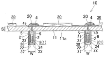
- the capacitor element manufacturing jig 10 includes a substrate 11 and a beam member 8.
- the beam member 8 includes a plurality of conductive sockets 1 and is mounted on the lower surface of the substrate 11.
- the socket 1 includes a conductive socket main body 2 having a lead wire insertion port 37 provided on the lower surface, and an insulating unit 5 that covers a part of the socket main body 2 in a manner that does not block the insertion port 37. (A part of the beam member 8) and a conductive lead wire portion 4 electrically connected to the socket body portion 2 (see FIGS. 4 and 6).
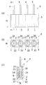
- a beam member 8 in which a plurality of sockets 1 are embedded in parallel at equal intervals is used as the plurality of sockets 1 (see FIGS. 3 and 6).
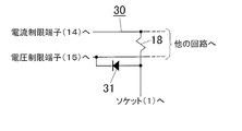
- An electric circuit 30 having a pair of electric terminals 14 and 15 is formed on the substrate 11 as shown in FIGS.
- the pair of electrical terminals 14 and 15 are electrically connected to a power supply source (hereinafter referred to as “power source”) 32 (see FIG. 9).
- power source a power supply source
- the electric circuit 30 has a circuit for limiting current (for example, the circuits of FIGS. 9 and 10), and each anode body (conductor) 52 via the socket 1 and the lead wire 53 connected thereto. Independently supply current. That is, the electric circuit 30 limits the current for each individual socket 1.
- the maximum current value flowing through each anode body (conductor) 52 is the current limit value of the electric circuit.
- the circuit for limiting the current is preferably a constant current circuit (for example, FIG. 9) in order to minimize the deviation of the obtained capacitor.
- the electric circuit 30 is a circuit for limiting the voltage for each individual socket 1. That is, the electric circuit 30 is more preferably a circuit that limits the voltage applied to each anode body (conductor) 52. In this case, even when a relatively large current is passed, the maximum voltage value applied to the anode body 52 is limited, so that the processing time for chemical formation and semiconductor layer formation can be shortened.
- the pair of electrical terminals 14 and 15 are provided at one end of the circuit board 11 in the width direction (see FIGS. 1 to 3).
- One electric terminal is a current limit terminal 14, and a current limit value is set by a voltage applied to the terminal 14.
- a current limit value is set by a voltage applied to the terminal 14.
- it can be set by the potential difference between the current limiting terminal 14 and the voltage limiting terminal 15 described later, and in the case of the circuit of FIG. 10, it can be set by the potential difference between the current limiting terminal 14 and the cathode plate 51.
- the other electrical terminal is a voltage limiting terminal 15, and the maximum voltage value applied to each anode body (conductor) 52 is limited by the voltage applied to the terminal 15.
- the maximum voltage value applied to each anode body (conductor) 52 is limited by the voltage applied to the terminal 15.
- it can be set by the potential difference between the voltage limiting terminal 15 and the cathode plate 51.
- a transistor 19 and a resistor 18 are mounted (attached) on the upper surface of the substrate 11, and an emitter E of the transistor 19 is electrically connected to one end of the resistor 18.
- the other end of the capacitor 18 is electrically connected to the current limiting terminal 14, the base B of the transistor 19 is electrically connected to the voltage limiting terminal 15, and the collector C of the transistor 19 is connected to the lead wire portion 4 of the socket 1. Is electrically connected.
- a part of the base end side of the lead wire portion 4 is disposed in a through hole 49 provided in the substrate 11 (see FIG. 4).
- the wire portion 4 is inserted from the lower surface side of the substrate 11, and the leading end of the lead wire portion 4 is electrically connected to the electric circuit 30 (see FIG. 4).
- a plurality of through holes 49 arranged in a second row (second row from one end in the width direction) along the length direction of the substrate 11 were embedded in another beam member 8.
- Each lead wire portion 4 of the socket 1 is inserted from the lower surface side of the substrate 11, and the leading end of the lead wire portion 4 is electrically connected to the electric circuit 30 (see FIG. 4).
- the lead wire portions 4 of the socket 1 embedded in the beam member 8 are inserted from the lower surface side of the substrate 11 with respect to the large number of through holes 49 in each row after the third row.
- the tip is electrically connected to the electric circuit 30 (see FIG. 4).
- the lead wire portion 4 is electrically connected to the electric circuit 30, whereby the socket 1 is electrically connected to the electric circuit 30 (see FIG. 4).
- the plurality of sockets 1 are mounted on the lower surface of the substrate 11 (see FIGS. 3 and 4).
- the length direction of the substrate 11 and the length direction of the beam member 8 are substantially coincident (including coincidence) (see FIG. 3).
- the electrical connection between the tip of the lead wire portion 4 and the electric circuit 30 is made by solder 20 (see FIGS. 4 and 5).
- lead wire insertion ports 37 of the plurality of sockets 1 mounted on the substrate 11 are opened downward on the lower surface side of the substrate 11.
- the lead wire 53 of the capacitor anode body 53 having the lead wire 53 is electrically connected to the insertion port 37 on the lower surface of the socket 1, the insertion direction of the lead wire 53 is relative to the lower surface of the substrate 11.
- the vertical direction see FIGS. 7 and 8).
- the electric circuit 30 in the capacitor element manufacturing jig 10 is not particularly limited to the one having the configuration shown in FIG. 9, and may have a circuit configuration as shown in FIG. In FIG. 10, 31 is a diode.
- the substrate 11 may be constituted by a single plate or a laminated plate in which a plurality of plates are laminated.
- a laminated plate as the substrate 11 for example, it may be a laminated plate in which the adjacent plates are simply overlapped without being bonded, or a laminated plate in which the adjacent plates are bonded together. There may be.
- An insulating substrate is used as the substrate 11.
- the material of the insulating substrate is not particularly limited, and examples thereof include insulating materials such as phenol resin, glass epoxy resin, and polyimide resin.
- the socket 1 used in this embodiment is shown in FIG.
- the socket 1 includes a conductive socket main body 2 and a conductive lead wire 4.
- a plurality of sockets 1 are embedded in the beam member 8 in parallel (see FIG. 6).
- the socket body 2 is a member that plays a role as an electrical connection terminal that is electrically connected to the anode body (conductor) 52 and the like, and is made of a conductive material such as a metal material in order to obtain electrical continuity.
- the metal constituting the socket body 2 is not particularly limited, but contains at least one metal selected from the group consisting of copper, iron, silver and aluminum as a main component (containing 50% by mass or more). It is preferable to use a metal (including an alloy).
- the surface of the socket main body 2 may be provided with at least one layer of conventionally known plating such as tin plating, solder plating, nickel plating, gold plating, silver plating, copper plating and the like.
- the socket main body 2 includes a cylindrical portion 21 and an inclined surface portion 22 that extends outward from the peripheral edge of the bottom surface of the cylindrical portion 21 downward (see FIG. 6). ),
- the cylindrical portion 21 and the inclined surface portion 22 are made of a conductive material such as a metal material.
- a lead wire insertion port 37 is formed by being surrounded by the inclined surface portion 22 (see FIG. 6).
- a hollow portion 23 having an opening on the bottom surface is provided inside the cylindrical portion 21. The hollow portion 23 communicates with the space of the lead wire insertion port 37.
- a metal spring member 24 is connected to the inner peripheral surface of the hollow portion 23, and a lead wire insertion hole 38 is formed by being surrounded by the metal spring member 24.
- the lead wire insertion hole 38 communicates with the space of the lead wire insertion port 37.
- the socket body 2 and the anode body (conductor) 52 are electrically connected. Connected.
- a lead wire portion 4 extends from the center of the upper surface of the socket body portion 2 (the upper surface of the cylindrical portion 21) (see FIG. 6).
- the lead wire portion 4 is made of a conductive material such as a metal material. That is, the lead wire portion 4 is formed integrally with the socket body portion 2 and is electrically connected to the socket body portion 2.
- Examples of the metal constituting the lead wire portion 4 include the same metals as exemplified as the metal constituting the socket main body portion 2.
- the lead wire portion 4 is usually made of the same metal as that constituting the socket body portion 2.
- a part of the socket main body 2 is covered with the resin insulating portion 5 so as not to block the lead wire insertion port 37.
- the entire peripheral side surface of the socket main body 2 is covered with the resin insulating portion 5 (see FIG. 6).
- each lead wire portion 4 of the socket 1 is inserted into each of the through holes 49 provided in the substrate 11 from the lower surface side of the substrate 11, and the upper surface of the beam member 8 is inserted into the lower surface of the substrate 11.
- the upper surface of the beam member 8 (the plurality of sockets 1) is fixed to the lower surface of the substrate 11 in a manner in contact with the lower surface of the substrate 11. It is mounted on the lower surface (see FIGS. 3 and 4).
- the beam member 8 includes an insulating portion 5 around at least the socket 1 in order to electrically insulate the sockets 1 from each other.
- the beam member 8 may be made of an insulating material and may also serve as an insulating portion.
- the material constituting the beam member 8 or the insulating portion 5 is not particularly limited, but is preferably an insulating material that is easy to process for providing the socket 1 and has higher rigidity. Examples thereof include hard resins such as epoxy resins, phenol resins, polyimide resins, polycarbonate resins, polyamide resins, polyamideimide resins, polyester resins, and polyphenylene sulfide resins.
- FIG. 7 is a schematic view showing an example of a method for manufacturing a capacitor element.
- FIG. 9 is a schematic diagram showing the method of manufacturing the capacitor element in terms of an electric circuit.
- the processing container 50 in which the processing liquid 59 is charged is prepared.
- the treatment liquid 59 include a chemical conversion treatment liquid for forming the dielectric layer 54 and a semiconductor layer forming solution for forming the semiconductor layer 55.
- an anode body (conductor) 52 having a lead wire 53 is connected to each socket 1 mounted on the lower surface of the substrate 11 of the capacitor element manufacturing jig 10 (see FIG. 8). Since the leading end side of the lead wire 53 is in contact with the metal spring member 24 in the cavity 23 of the socket main body 2, the socket 1 and the anode body (conductor) 52 are electrically connected ( (See FIG. 8). Thereby, the anode body 52 is electrically connected to the electric circuit 30 of the substrate 11 (see FIGS. 7 and 9). The lead wire 53 is inserted into the socket 1 in a direction perpendicular to the substrate 11 (see FIGS. 7 and 8).
- the capacitor element manufacturing jig 10 on which the anode body (conductor) 52 is set is horizontally disposed above the processing container 50, and the manufacturing jig 10 is in a horizontal state (the lower surface of the substrate 11).
- the jig 10 is lowered to a state in which at least a part (usually all) of the anode body (conductor) 52 is immersed in the treatment liquid 59 while maintaining the horizontal position).
- the jig 10 is fixed (see FIG. 7).
- the anode body 52 is used as an anode, and the cathode plate 51 disposed in the treatment liquid 59 is used as a cathode (see FIGS. 7 and 9).
- a chemical conversion treatment liquid is used as the first treatment liquid 59, a dielectric layer 54 (see FIG. 11) can be formed on the surface of the conductor 52 by the energization (dielectric layer forming step).
- the anode body 52 provided with the dielectric layer 54 on the surface is washed with water and dried, and then a semiconductor layer forming solution 59 is newly introduced into a processing container 50 different from the above, Similarly, the jig 10 is held in a horizontal state (the bottom surface of the substrate 11 is horizontal) until at least a part (usually all) of the anode body 52 is immersed in the semiconductor layer forming solution 59.
- the jig 10 is fixed at the height position, the anode body 52 is used as an anode, and the cathode plate 51 disposed in the semiconductor layer forming solution 59 is used as a cathode. That is, the second treatment is performed.
- the semiconductor layer 55 can be formed on the surface of the dielectric layer 54 on the surface of the anode body 52 (semiconductor layer forming step).
- Body layer 54 is laminated, It can further semiconductor layer 55 on the surface of the collector layer 54 to produce a capacitor element 56 formed by stacking (see FIG. 11).
- heat treatment is performed on the anode body 52 between the dielectric layer forming step and the semiconductor layer forming step and / or after the semiconductor layer forming step. May be.
- the size of the beam member 8 is not particularly limited, but may be a size according to the arrangement of the capacitor elements when immersed in the processing liquid 59.
- the width W of the beam member 8 is preferably 1.6 mm to 5.1 mm, more preferably 2 mm to 3 mm.
- the height H of the beam member 8 is preferably 2 mm to 10 mm, more preferably 3 mm to 5 mm.
- the length L of the beam member 8 is longer than the length that can accommodate at least the required number of sockets 1 and is preferably in a range that does not protrude from the substrate 11, and is preferably longer in this range. If it is in the range of such a dimension, it will be easy to carry a machine and it will be easy to obtain the jig
- the anode body 52 is not particularly limited, and examples thereof include at least one anode body selected from the group consisting of a valve metal and a conductive oxide of the valve metal. Specific examples thereof include aluminum, tantalum, niobium, titanium, zirconium, niobium monoxide, zirconium monoxide and the like.
- the shape of the anode body 52 is not particularly limited, and examples thereof include a foil shape, a plate shape, a rod shape, and a rectangular parallelepiped shape.
- the chemical conversion treatment liquid 59 is not particularly limited.
- an organic acid or a salt thereof for example, adipic acid, acetic acid, ammonium adipate, benzoic acid, etc.
- an inorganic acid or a salt thereof for example, phosphoric acid
- examples thereof include a solution in which a conventionally known electrolyte such as silicic acid, ammonium phosphate, ammonium silicate, sulfuric acid, ammonium sulfate or the like is dissolved or suspended.
- the surface of the anode body 52 contains an insulating metal oxide such as Ta 2 O 5 , Al 2 O 3 , Zr 2 O 3 , Nb 2 O 5 or the like.
- a dielectric layer 54 can be formed.
- the dielectric layer forming step using such a chemical conversion treatment solution may be omitted, and the anode body 52 having the dielectric layer 54 already provided on the surface may be used for the semiconductor layer forming step.
- Examples of such a surface dielectric layer 54 include a dielectric layer mainly composed of at least one selected from insulating oxides, and a conventionally known dielectric layer in the field of ceramic capacitors and film capacitors.
- the semiconductor layer forming solution 59 is not particularly limited as long as it can form a semiconductor by energization.
- examples thereof include solutions containing oxythiophene and the like.
- a dopant may be further added to the semiconductor layer forming solution 59.
- well-known dopants such as aryl sulfonic acid or its salt, alkyl sulfonic acid or its salt, various polymeric sulfonic acid or its salt, etc. are mentioned.
- a conductive polymer for example, polyaniline, polythiophene, polypyrrole, polymethylpyrrole, etc.
- the semiconductor layer 55 made of can be formed.
- an electrode layer is formed on the semiconductor layer 55 of the capacitor element 56 obtained by the above manufacturing method in order to improve electrical contact with an electrode terminal (for example, a lead frame) for external extraction of the capacitor. It may be provided.
- the electrode layer can be formed by, for example, solidifying a conductive paste, plating, metal deposition, or forming a heat-resistant conductive resin film.
- a conductive paste As the conductive paste, silver paste, copper paste, aluminum paste, carbon paste, nickel paste and the like are preferable.
- Electrode terminals are electrically connected to the anode body 52 and the semiconductor layer 55 of the capacitor element 56 thus obtained (for example, the lead wire 53 is welded to one electrode terminal, and the electrode layer (semiconductor layer) 55 is connected. Is adhered to the other electrode terminal with a silver paste or the like), and the capacitor is obtained by sealing with leaving a part of the electrode terminal.
- the sealing method is not particularly limited, and examples thereof include a resin mold exterior, a resin case exterior, a metal case exterior, a resin dipping exterior, and a laminate film exterior.
- a resin mold exterior is preferable because it can be easily reduced in size and cost.
- An electric circuit 30 or the like serving as a power source for supplying current to the anode body shown in FIGS. 2 and 5 described in detail in the previous section is formed on the substrate 11.
- a current limiting terminal 14 and a voltage limiting terminal 15 are provided at an intermediate portion of one of the pair of edges extending in the length direction of the upper surface of the substrate 11 (FIGS. 1 and 2). reference).
- each transistor 19 was mounted on the substrate 11 with the configuration shown in FIGS. 2 to 5 and 9 described in detail in the previous section.
- the collector C of each transistor 19 is an output as a power source.
- the resistor 18, 1 K ⁇ (error within ⁇ 0.5%) was used, and as the transistor 19, “transistor 2SA2154” manufactured by Toshiba was used.
- a beam member 8 made of polyphenylene sulfide resin (length L: 165.1 mm, width W: 2.54 mm, height H: 4.5 mm) was prepared.
- 64 sockets 1 are embedded in parallel at a pitch of 2.54 mm, and each lead wire portion 4 of the socket 1 is drawn from the upper surface of the beam member 8 (see FIG. 6).
- Each of the lead wire portions 4 of the beam member 8 is inserted into each of the 640 through holes 49 provided in the substrate 11 from the lower surface side of the substrate 11, and the upper surface of the beam member 8 is disposed on the lower surface of the substrate 11. It is glued. Further, the lead wire portion 4 is electrically connected to the output of the power source (see FIGS. 4 and 5). Thus, the ten beam members 8 are mounted in parallel on the lower surface of the substrate 11 (see FIGS. 3, 4, 7, and 8).
- both edges in the longitudinal direction of the beam member 8 of the jig 10 for manufacturing the solid electrolytic capacitor element are connected to a machine transfer device (illustrated).
- the substrate 11 is held horizontally by being gripped by the gripping portion 40.
- an anode body (conductor) 52 having a lead wire 53 is connected to each of the plurality of sockets 1 mounted on the lower surface of the substrate 11 of the capacitor element manufacturing jig 10.
- the lead wire 53 is inserted into the socket 1 in a direction perpendicular to the substrate 11 (see FIGS. 7 and 8).
- the capacitor element manufacturing jig 10 in which the anode body (conductor) 52 is set is positioned above a processing vessel 50 made of metal (stainless steel) containing a 2 mass% phosphoric acid aqueous solution (processing solution) 59 therein. And placed horizontally.
- the metal processing vessel 50 also serves as the cathode plate 51.
- the jig 10 is lowered while maintaining the horizontal state so that the whole of the anode body 52 and the lower end 5 mm of the lead wire 53 are immersed in the processing liquid 59. Fixed in position (see FIG. 7). In this immersed state, a voltage is applied between the voltage limiting terminal 15 and the cathode plate (including the metal processing vessel 50) 51 so that the voltage limiting value (chemical conversion voltage) is 8.3 V, and each anode body The current was applied by applying a voltage between the current limiting terminal 14 and the voltage limiting terminal 15 so that the current limiting value of the current was 2.1 mA.
- the pores and the outer surface of the conductive sintered body 52 and the surface of a part of the lead wire (for 5 mm) are formed.
- a dielectric layer 54 was formed.
- the current limit value was continuously decreased at a rate of 0.5 mA per hour for the latter 4 hours from 4 hours to 8 hours (dielectric layer forming step).
- the anode body 52 having the dielectric layer 54 on the surface is washed with water and dried, and then immersed in a 20% by mass ethylenedioxythiophene ethanol solution, while the semiconductor is contained in a processing container 50 different from the processing container 50.
- Layer forming solution 59 (a solution in which 0.4% by mass of ethylenedioxythiophene and 0.6% by mass of anthraquinone sulfonic acid were mixed in a mixed solvent consisting of 70 parts by mass of water and 30 parts by mass of ethylene glycol) was added.
- the jig 10 is kept in a horizontal state so that the whole anode body 52 having the dielectric layer 54 on the surface and the lower end 5 mm of the lead wire 53 are immersed in the semiconductor layer forming solution 59. It was lowered and fixed at that height position. In this immersed state, electrolytic polymerization was carried out at 20 ° C. with a constant current of 5 ⁇ A per anode body for 50 minutes. Thereafter, the anode body 52 provided with the dielectric layer 54 on the surface thereof was pulled up from the solution 59, washed with water, washed with alcohol, and dried.
- Dielectric layer 54 was formed on the surface by performing such electrolytic polymerization (electropolymerization for 50 minutes at a constant current of 5 ⁇ A per anode body), water washing, alcohol washing, and drying six more times.
- a semiconductor layer 55 made of a conductive polymer was formed on the surface of the dielectric layer 54 of the anode body 52 (semiconductor layer forming step).
- the dielectric layer 54 was repaired by re-forming. This re-chemical conversion was performed for 15 minutes using the same solution as that used in the anodic oxidation at a limiting voltage of 6.3 V and a limiting current of 0.1 mA for each anode body (re-forming process).
- the substrate 11 with the anode body 52 connected to the socket 1 is heated to 150 ° C. Drying was performed by leaving it in the atmosphere for 3 hours (carbon layer forming step).
- the anode body 52 formed by laminating the dielectric layer 54, the semiconductor layer 55, and the carbon layer is washed with water and dried, and then a silver paste is applied to the surface of the carbon layer, and then the anode body 52 is connected to the socket 1. Drying was performed by leaving the substrate 11 in a state in which it was left in an atmosphere of 150 ° C. for 4 hours (silver paste lamination step). In this way, a capacitor element 56 was obtained.
- capacitor elements 56 can be manufactured through the above-described series of steps. By performing this process three more times (that is, four times in total), a total of 2560 capacitor elements 56 were manufactured.
- Example 1 A capacitor element manufacturing jig was obtained in the same manner as in Example 1 except that the beam member was not used and 640 pieces were individually mounted directly on the substrate 11 without embedding the socket 1 in the beam member. That is, the socket 1 is inserted into the through hole 49 of the substrate 11 (having a hole diameter into which the cylindrical portion 21 of the socket 1 is inserted) so that the upper surface of the socket 1 is flush with the upper surface of the substrate. Were individually (in an independent state) fixed with a filler in a state where the lead wire insertion port was directed toward the lower surface of the substrate 11. Each socket 1 is electrically connected to an output of a power source configured on the substrate 11 as in the first embodiment.
- an anode body (conductor) 52 having a lead wire 53 was connected to each of the plurality of sockets 1 mounted on the lower surface of the substrate in the same manner as in Example 1.
- capacitor elements 56 can be manufactured through the above-described series of steps. By performing this process three more times (that is, four times in total), a total of 2560 capacitor elements 56 were manufactured.
- the number of elements in which the semiconductor layer protruded from the base (base end) of the lead wire 53 above the polytetrafluoroethylene washer (thickness: 0.10 mm) was 1352.
- the comparative example 1 since the third implementation, distortion deformation is relatively remarkably generated in the glass epoxy substrate held horizontally, and after the third implementation, the semiconductor layer protrudes from the position above the washer. The number of formed elements has increased remarkably.
- the term present invention or inventory should not be construed inappropriately as identifying criticality, nor should it be construed as inappropriately applied across all aspects or all embodiments ( That is, the present invention should be understood to have numerous aspects and embodiments) and should not be construed inappropriately to limit the scope of the present application or the claims.
- the term “embodiment” is also used to describe any aspect, feature, process or step, any combination thereof, and / or any part thereof. It is done. In some examples, various embodiments may include overlapping features.
- the abbreviations “e.g.,” and “NB” may be used, meaning “for example” and “carefully”, respectively.
- the capacitor element manufacturing jig according to the present invention is suitably used as an electrolytic capacitor element manufacturing jig, but is not particularly limited to such applications. Further, the capacitor obtained by the manufacturing method of the present invention can be used for digital devices such as personal computers, cameras, game machines, AV devices, and mobile phones, and electronic devices such as various power sources.
Landscapes
- Engineering & Computer Science (AREA)
- Power Engineering (AREA)
- Microelectronics & Electronic Packaging (AREA)
- Manufacturing & Machinery (AREA)
- Chemical & Material Sciences (AREA)
- Chemical Kinetics & Catalysis (AREA)
- Electrochemistry (AREA)
- Materials Engineering (AREA)
- Metallurgy (AREA)
- Organic Chemistry (AREA)
- Fixed Capacitors And Capacitor Manufacturing Machines (AREA)
Abstract
Description
前記基板の少なくとも片面に並列に配置された複数の梁部材と、
前記梁部材に設けられた複数個の導電性のソケットと、を備え、
前記複数個のソケットは、コンデンサ用陽極体に電流を供給する電源に電気的に接続可能であり、
前記ソケットは、リード線を有するコンデンサ用陽極体のリード線を電気接続する際の該リード線の差込口を有し、前記差込口が前記基板の下方向に開かれていることを特徴とするコンデンサ素子製造用治具。
個々の前記ソケットは、それぞれ個々の前記電源に電気的に接続され、前記電源に接続されていることを除き相互に電気的に絶縁されている前項1~3のいずれか1項に記載のコンデンサ素子製造用治具。
前記治具の基板が、前記梁部材の長手方向の両縁部において把持されて、水平に保持された状態にあり、かつ、
前記陽極体が化成処理液中に浸漬された状態で、
前記陽極体を陽極にして通電することによって、前記陽極体の表面に誘電体層を形成する誘電体層形成工程を含むことを特徴とするコンデンサ素子の製造方法。
前記治具の基板が、前記梁部材の長手方向の両縁部において把持されて、水平に保持された状態にあり、かつ、
前記陽極体が半導体層形成用溶液中に浸漬された状態で、
前記陽極体を陽極にして通電することによって、前記陽極体表面の誘電体層の表面に半導体層を形成する半導体層形成工程を含むことを特徴とするコンデンサ素子の製造方法。
前記治具の基板が、前記梁部材の長手方向の両縁部において把持されて、水平に保持された状態にあり、かつ、
前記陽極体が化成処理液中に浸漬された状態で、
前記陽極体を陽極にして通電することによって、前記陽極体の表面に誘電体層を形成する誘電体層形成工程と、
前記誘電体層形成工程の後に、陽極体がソケットに接続された状態の前記基板が水平に保持された状態にあり、かつ、
前記陽極体が半導体層形成用溶液中に浸漬された状態で、
前記陽極体を陽極にして通電することによって、前記陽極体表面の誘電体層の表面に半導体層を形成する半導体層形成工程と、を含むことを特徴とするコンデンサ素子の製造方法。
[陽極体(導電体)52の作製]
長さ0.80mm×幅0.53mm×厚さ0.43mmの直方体形状のタンタル焼結体(陽極体)52の0.53mm×0.43mmの面(上面)に、長さ10.4±0.3mm、直径0.15mmのタンタル線(リード線)53が植立されたものを640個準備した。更に、外径0.40mm、内径0.10mm、厚さ0.10mmのポリテトラフルオロエチレン製の環状のワッシャーをリード線53の根元まで装着した(外装した)。
(電子部品が実装された基板)
長さ180mm×幅96mm×厚さ1.6mmのガラスエポキシ基板を準備した。このガラスエポキシ基板には、該基板の長さ方向に沿って64個の貫通孔49が2.54mmピッチで形成され、これら一列に延びた64個の貫通孔49の群が、基板11の幅方向に沿って8mmピッチで合計で10列形成されている(なお、図面では、作図上の理由により9列のみ記載している)。即ち、前記ガラスエポキシ基板11には、合計で640個の貫通孔49が形成されている。
図7に示すように、前記固体電解コンデンサ素子製造用治具10の梁部材8の長手方向の両縁部(図7の基板11の長さ方向の両縁部)を、機械搬送装置(図示しない)の把持部40で把持することによって、基板11を水平に保持する。
梁部材を用いず、また、ソケット1を梁部材に埋設せずに640個をそれぞれ個別に基板11に直接実装した以外は、実施例1と同様にしてコンデンサ素子製造用治具を得た。即ち、基板11の貫通孔49(前記ソケット1の円柱部21が入る穴径になっている)内に、ソケット1の上面が基板上面と面一になるようにソケット1を挿通して、ソケットを個別に(独立した状態で)基板11の下面方向にリード線差込口を向けた状態で充填材で固定した。また、各ソケット1は、実施例1と同様に基板11に構成された電源の出力にそれぞれ電気的に接続されている。
2…ソケット本体部
4…リード線部
5…絶縁部
8…梁部材
10…コンデンサ素子製造用治具
11…基板
14…電流制限端子
15…電圧制限端子
18…抵抗器
19…トランジスタ
30…電気回路
32…電源
37…リード線差込口
49…貫通孔
51…陰極板
52…陽極体(導電体)
53…リード線
54…誘電体層
55…半導体層
56…コンデンサ素子
59…処理液(化成処理液、半導体層形成用溶液)
Claims (10)
- 基板と、
前記基板の少なくとも片面に並列に配置された複数の梁部材と、
前記梁部材に設けられた複数個の導電性のソケットと、を備え、
前記複数個のソケットは、コンデンサ用陽極体に電流を供給する電源に電気的に接続可能であり、
前記ソケットは、リード線を有するコンデンサ用陽極体のリード線を電気接続する際の該リード線の差込口を有し、前記差込口が前記基板の下方向に開かれていることを特徴とするコンデンサ素子製造用治具。 - 前記梁部材は、幅1.6mm~5.1mm、高さ2mm~10mmである請求項1に記載のコンデンサ素子製造用治具。
- 前記梁部材は、硬質樹脂を含有してなる請求項1または2に記載のコンデンサ素子製造用治具。
- 前記電源は、前記基板の少なくとも片面に形成された電気回路からなり、
個々の前記ソケットは、それぞれ個々の前記電源に電気的に接続され、前記電源に接続されていることを除き相互に電気的に絶縁されている請求項1~3のいずれか1項に記載のコンデンサ素子製造用治具。 - 前記電気回路が定電流回路である請求項4に記載のコンデンサ素子製造用治具。
- 前記電気回路は、個々の前記ソケット毎に電圧を制限する回路でもある請求項4または5に記載のコンデンサ素子製造用治具。
- 請求項1~6のいずれか1項に記載のコンデンサ素子製造用治具のソケットにコンデンサ用陽極体が接続されると共に、
前記治具の基板が、前記梁部材の長手方向の両縁部において把持されて、水平に保持された状態にあり、かつ、
前記陽極体が化成処理液中に浸漬された状態で、
前記陽極体を陽極にして通電することによって、前記陽極体の表面に誘電体層を形成する誘電体層形成工程を含むことを特徴とするコンデンサ素子の製造方法。 - 請求項1~6のいずれか1項に記載のコンデンサ素子製造用治具のソケットに、表面に誘電体層が設けられた陽極体が接続されると共に、
前記治具の基板が、前記梁部材の長手方向の両縁部において把持されて、水平に保持された状態にあり、かつ、
前記陽極体が半導体層形成用溶液中に浸漬された状態で、
前記陽極体を陽極にして通電することによって、前記陽極体表面の誘電体層の表面に半導体層を形成する半導体層形成工程を含むことを特徴とするコンデンサ素子の製造方法。 - 請求項1~6のいずれか1項に記載のコンデンサ素子製造用治具のソケットにコンデンサ用陽極体を接続されると共に、
前記治具の基板が、前記梁部材の長手方向の両縁部において把持されて、水平に保持された状態にあり、かつ、
前記陽極体が化成処理液中に浸漬された状態で、
前記陽極体を陽極にして通電することによって、前記陽極体の表面に誘電体層を形成する誘電体層形成工程と、
前記誘電体層形成工程の後に、陽極体がソケットに接続された状態の前記基板が水平に保持された状態にあり、かつ、
前記陽極体が半導体層形成用溶液中に浸漬された状態で、
前記陽極体を陽極にして通電することによって、前記陽極体表面の誘電体層の表面に半導体層を形成する半導体層形成工程と、を含むことを特徴とするコンデンサ素子の製造方法。 - 請求項7~9のいずれか1項に記載の製造方法で得たコンデンサ素子の陽極体及び半導体層に、それぞれ電極端子を電気的に接続し、前記電極端子の一部を残して封止するコンデンサの製造方法。
Priority Applications (4)
| Application Number | Priority Date | Filing Date | Title |
|---|---|---|---|
| CN201280064402.7A CN104025226B (zh) | 2011-12-28 | 2012-09-05 | 电容器元件制造用夹具和电容器元件的制造方法 |
| JP2012554151A JP5269261B1 (ja) | 2011-12-28 | 2012-09-05 | コンデンサ素子製造用治具及びコンデンサ素子の製造方法 |
| EP12863673.5A EP2800115A4 (en) | 2011-12-28 | 2012-09-05 | TEMPLATE FOR MANUFACTURING CAPACITOR ELEMENT AND METHOD FOR MANUFACTURING CAPACITOR ELEMENT |
| US14/368,819 US9251954B2 (en) | 2011-12-28 | 2012-09-05 | Jig for manufacturing capacitor element and method for manufacturing capacitor element |
Applications Claiming Priority (2)
| Application Number | Priority Date | Filing Date | Title |
|---|---|---|---|
| JP2011-288070 | 2011-12-28 | ||
| JP2011288070 | 2011-12-28 |
Publications (1)
| Publication Number | Publication Date |
|---|---|
| WO2013099361A1 true WO2013099361A1 (ja) | 2013-07-04 |
Family
ID=48696868
Family Applications (1)
| Application Number | Title | Priority Date | Filing Date |
|---|---|---|---|
| PCT/JP2012/072587 WO2013099361A1 (ja) | 2011-12-28 | 2012-09-05 | コンデンサ素子製造用治具及びコンデンサ素子の製造方法 |
Country Status (5)
| Country | Link |
|---|---|
| US (1) | US9251954B2 (ja) |
| EP (1) | EP2800115A4 (ja) |
| JP (1) | JP5269261B1 (ja) |
| CN (1) | CN104025226B (ja) |
| WO (1) | WO2013099361A1 (ja) |
Citations (4)
| Publication number | Priority date | Publication date | Assignee | Title |
|---|---|---|---|---|
| JPH09186053A (ja) * | 1995-12-28 | 1997-07-15 | Matsushita Electric Ind Co Ltd | アルミ電解コンデンサ用電極端子 |
| WO2010107011A1 (ja) | 2009-03-17 | 2010-09-23 | 昭和電工株式会社 | 固体電解コンデンサ素子、その製造方法及びその製造用冶具 |
| WO2011074512A1 (ja) * | 2009-12-15 | 2011-06-23 | 昭和電工株式会社 | ソケット及び該ソケットを用いたコンデンサ素子製造用治具 |
| JP2011238740A (ja) * | 2010-05-10 | 2011-11-24 | Murata Mfg Co Ltd | コンデンサ製造用治具及びコンデンサ製造方法 |
Family Cites Families (6)
| Publication number | Priority date | Publication date | Assignee | Title |
|---|---|---|---|---|
| US4896813A (en) | 1989-04-03 | 1990-01-30 | Toyo Kohan Co., Ltd. | Method and apparatus for cold rolling clad sheet |
| EP0735616A3 (de) | 1995-03-31 | 1997-03-19 | Wieland Elektrische Industrie | Elektrischer Steckverbinder insbesondere für Leiterplatten |
| US6960092B1 (en) * | 2003-07-25 | 2005-11-01 | Advanced Micro Devices, Inc. | Compression mount and zero insertion force socket for IC devices |
| JP4050306B2 (ja) * | 2005-03-24 | 2008-02-20 | 昭和電工株式会社 | 固体電解コンデンサの製造装置及び製造方法 |
| US7602201B2 (en) * | 2007-06-22 | 2009-10-13 | Qualitau, Inc. | High temperature ceramic socket configured to test packaged semiconductor devices |
| JP5829403B2 (ja) | 2010-05-18 | 2015-12-09 | 昭和電工株式会社 | 放熱用絶縁基板及びその製造方法 |
-
2012
- 2012-09-05 JP JP2012554151A patent/JP5269261B1/ja not_active Expired - Fee Related
- 2012-09-05 EP EP12863673.5A patent/EP2800115A4/en not_active Withdrawn
- 2012-09-05 CN CN201280064402.7A patent/CN104025226B/zh not_active Expired - Fee Related
- 2012-09-05 US US14/368,819 patent/US9251954B2/en not_active Expired - Fee Related
- 2012-09-05 WO PCT/JP2012/072587 patent/WO2013099361A1/ja active Application Filing
Patent Citations (4)
| Publication number | Priority date | Publication date | Assignee | Title |
|---|---|---|---|---|
| JPH09186053A (ja) * | 1995-12-28 | 1997-07-15 | Matsushita Electric Ind Co Ltd | アルミ電解コンデンサ用電極端子 |
| WO2010107011A1 (ja) | 2009-03-17 | 2010-09-23 | 昭和電工株式会社 | 固体電解コンデンサ素子、その製造方法及びその製造用冶具 |
| WO2011074512A1 (ja) * | 2009-12-15 | 2011-06-23 | 昭和電工株式会社 | ソケット及び該ソケットを用いたコンデンサ素子製造用治具 |
| JP2011238740A (ja) * | 2010-05-10 | 2011-11-24 | Murata Mfg Co Ltd | コンデンサ製造用治具及びコンデンサ製造方法 |
Non-Patent Citations (1)
| Title |
|---|
| See also references of EP2800115A4 |
Also Published As
| Publication number | Publication date |
|---|---|
| JPWO2013099361A1 (ja) | 2015-04-30 |
| CN104025226B (zh) | 2017-06-30 |
| CN104025226A (zh) | 2014-09-03 |
| EP2800115A4 (en) | 2015-10-14 |
| US9251954B2 (en) | 2016-02-02 |
| US20140366350A1 (en) | 2014-12-18 |
| JP5269261B1 (ja) | 2013-08-21 |
| EP2800115A1 (en) | 2014-11-05 |
Similar Documents
| Publication | Publication Date | Title |
|---|---|---|
| JP5079850B2 (ja) | コンデンサの製造方法 | |
| US9305712B2 (en) | Tantalum capacitor and method of manufacturing the same | |
| JP6184872B2 (ja) | コンデンサ素子製造用治具及びコンデンサ素子の製造方法 | |
| US7919383B2 (en) | Capacitor element manufacturing jig and capacitor element manufacturing method | |
| KR101477446B1 (ko) | 연결 소켓, 상기 연결 소켓을 사용한 콘덴서 소자 제조용 지그, 콘덴서 소자의 제조 방법, 및 콘덴서의 제조 방법 | |
| JP5135476B2 (ja) | ソケット及び該ソケットを用いたコンデンサ素子製造用治具 | |
| JP5269261B1 (ja) | コンデンサ素子製造用治具及びコンデンサ素子の製造方法 | |
| WO2012035899A1 (ja) | 固体電解コンデンサ素子、その製造方法及びその製造用冶具 | |
| JP2011238740A (ja) | コンデンサ製造用治具及びコンデンサ製造方法 | |
| JP2014192231A (ja) | 固体電解コンデンサの製造方法 |
Legal Events
| Date | Code | Title | Description |
|---|---|---|---|
| ENP | Entry into the national phase |
Ref document number: 2012554151 Country of ref document: JP Kind code of ref document: A |
|
| 121 | Ep: the epo has been informed by wipo that ep was designated in this application |
Ref document number: 12863673 Country of ref document: EP Kind code of ref document: A1 |
|
| NENP | Non-entry into the national phase |
Ref country code: DE |
|
| WWE | Wipo information: entry into national phase |
Ref document number: 2012863673 Country of ref document: EP |
|
| WWE | Wipo information: entry into national phase |
Ref document number: 14368819 Country of ref document: US |