WO2013094716A1 - プラズマ生成装置及びプラズマ処理装置 - Google Patents
プラズマ生成装置及びプラズマ処理装置 Download PDFInfo
- Publication number
- WO2013094716A1 WO2013094716A1 PCT/JP2012/083181 JP2012083181W WO2013094716A1 WO 2013094716 A1 WO2013094716 A1 WO 2013094716A1 JP 2012083181 W JP2012083181 W JP 2012083181W WO 2013094716 A1 WO2013094716 A1 WO 2013094716A1
- Authority
- WO
- WIPO (PCT)
- Prior art keywords
- plasma
- plasma generation
- chamber
- waveguide
- processing apparatus
- Prior art date
- Legal status (The legal status is an assumption and is not a legal conclusion. Google has not performed a legal analysis and makes no representation as to the accuracy of the status listed.)
- Ceased
Links
Images

























Classifications
-
- H—ELECTRICITY
- H01—ELECTRIC ELEMENTS
- H01J—ELECTRIC DISCHARGE TUBES OR DISCHARGE LAMPS
- H01J37/00—Discharge tubes with provision for introducing objects or material to be exposed to the discharge, e.g. for the purpose of examination or processing thereof
- H01J37/32—Gas-filled discharge tubes
- H01J37/32009—Arrangements for generation of plasma specially adapted for examination or treatment of objects, e.g. plasma sources
- H01J37/32192—Microwave generated discharge
- H01J37/32201—Generating means
-
- H—ELECTRICITY
- H01—ELECTRIC ELEMENTS
- H01J—ELECTRIC DISCHARGE TUBES OR DISCHARGE LAMPS
- H01J37/00—Discharge tubes with provision for introducing objects or material to be exposed to the discharge, e.g. for the purpose of examination or processing thereof
- H01J37/32—Gas-filled discharge tubes
- H01J37/32009—Arrangements for generation of plasma specially adapted for examination or treatment of objects, e.g. plasma sources
- H01J37/32192—Microwave generated discharge
- H01J37/32211—Means for coupling power to the plasma
- H01J37/32229—Waveguides
-
- H—ELECTRICITY
- H01—ELECTRIC ELEMENTS
- H01J—ELECTRIC DISCHARGE TUBES OR DISCHARGE LAMPS
- H01J37/00—Discharge tubes with provision for introducing objects or material to be exposed to the discharge, e.g. for the purpose of examination or processing thereof
- H01J37/32—Gas-filled discharge tubes
- H01J37/32009—Arrangements for generation of plasma specially adapted for examination or treatment of objects, e.g. plasma sources
- H01J37/32192—Microwave generated discharge
- H01J37/32211—Means for coupling power to the plasma
- H01J37/32238—Windows
-
- H—ELECTRICITY
- H01—ELECTRIC ELEMENTS
- H01J—ELECTRIC DISCHARGE TUBES OR DISCHARGE LAMPS
- H01J37/00—Discharge tubes with provision for introducing objects or material to be exposed to the discharge, e.g. for the purpose of examination or processing thereof
- H01J37/32—Gas-filled discharge tubes
- H01J37/32431—Constructional details of the reactor
- H01J37/32458—Vessel
- H01J37/32477—Vessel characterised by the means for protecting vessels or internal parts, e.g. coatings
Definitions
- the present invention relates to a plasma generation apparatus and a plasma processing apparatus that generate plasma using microwaves.
- a number of plasma processing apparatuses that generate plasma from a processing gas and perform processing on the substrate by the plasma have been used.
- a high-frequency electric field is generated by supplying high-frequency power to two flat electrodes arranged in parallel, and plasma is generated by various reactions between electrons accelerated by the electric field and the processing gas.
- a parallel plate type plasma processing apparatus for performing plasma processing on a substrate with the plasma is generally used.
- plasma processing apparatuses using microwaves instead of high frequencies are also used.
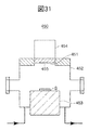
- FIG. 31 is a cross-sectional view schematically showing the configuration of a plasma processing apparatus using microwaves.
- a plasma processing apparatus 450 includes a vacuum chamber 452 having an opening 451 for introducing a microwave at the upper center, and a substrate mounting table 453 disposed inside the vacuum chamber 452 for mounting a substrate S. And a waveguide 454 for introducing microwaves into the opening 451 and a dielectric window 455 for introducing microwaves from the waveguide 454 into the vacuum chamber 452.
- plasma is generated by microwaves from the processing gas introduced into the vacuum chamber 452, and, for example, diamond is grown on the substrate S on the substrate mounting table 453 by radicals in the plasma (for example, see Patent Document 1).
- the plasma cuts off the microwave transmitted through the dielectric window 455.
- resonance absorption occurs at a position where the electron plasma (angular) frequency matches the microwave frequency.
- plasma is actively generated in the vicinity of the dielectric window 455. If plasma is generated under relatively high pressure conditions, the temperature of the processing gas becomes very high, and the dielectric window 455 may be damaged by heat, and a desired plasma is generated around the substrate S that is the object to be processed. In some cases, it cannot be generated.
- An object of the present invention is to provide a plasma generation apparatus and a plasma processing apparatus capable of preventing a dielectric window for introducing a microwave from being damaged and generating plasma in a desired region around a substrate. It is in.
- a waveguide for propagating microwaves a plasma generation chamber connected to the waveguide, the waveguide and the plasma generation
- a plasma generation apparatus comprising: a dielectric window interposed between chambers for introducing the microwave propagating through the waveguide into the plasma generation chamber.
- the plasma generation chamber has a spherical shape (including a polyhedral shape approximating a spherical shape and a spatial shape formed by a curved surface represented by a higher-order function) and accommodates a substrate.
- the plasma generation chamber is disposed adjacent to the processing chamber, and the inside of the plasma generation chamber communicates with the inside of the processing chamber.
- the waveguide is preferably arranged symmetrically with respect to the central axis of the plasma generation chamber.
- the plasma generation chamber has a hemispherical curved surface that is concentrically opposed to the hemispherical curved surface at a predetermined interval. It is preferable to include a hemispherical curved space portion sandwiched between hollow hemispherical inner curved surfaces having a diameter larger than that of the inner diameter.
- the plasma generation chamber is disposed adjacent to a processing chamber containing a substrate, and the inside of the plasma generation chamber communicates with the inside of the processing chamber.
- the waveguide is preferably arranged symmetrically with respect to the central axis of the plasma generation chamber.
- a waveguide for propagating microwaves, a plasma generation chamber connected to the waveguide, and the plasma generation chamber are arranged.
- a mounting table for mounting a substrate; and a dielectric window interposed between the waveguide and the plasma generation chamber for introducing the microwave propagating through the waveguide into the plasma generation chamber.
- the plasma generation chamber has a central axis and has a symmetrical shape with respect to the central axis.
- the plasma generation chamber preferably has a hemispherical shape.
- the plasma generation chamber is preferably cut away at a portion facing the mounting table.
- the plasma generation chamber preferably has a conical shape.
- the plasma generation chamber is preferably cut away at a portion facing the mounting table.
- a protruding member facing the mounting table is disposed in the plasma generation chamber.
- the protruding member is disposed offset from a central axis of the plasma generation chamber.
- the protruding member is preferably configured to be movable.
- the apparatus includes a processing chamber that accommodates a substrate, and a plasma generation device that is disposed adjacent to the processing chamber.
- a waveguide for propagating microwaves, a plasma generation chamber connected to the waveguide, and interposed between the waveguide and the plasma generation chamber, the microwave propagating through the waveguide is there is provided a plasma processing apparatus having a dielectric window introduced into the inside of the plasma generation chamber, wherein the inside of the plasma generation chamber communicates with the inside of the processing chamber.
- the plasma generation chamber preferably has a spherical shape.
- the plasma generation chamber has a hemispherical curved surface and the hemispherical curved surface that is concentrically opposed to the hemispherical curved surface at a predetermined interval. It is preferable to have a hemispherical curved space sandwiched between hollow hemispherical inner curved surfaces having a diameter larger than the diameter.
- the plasma generation chamber into which the microwave is introduced has a spherical shape
- the radius of the plasma generation chamber that is a boundary condition of the electromagnetic wave existing in the plasma generation chamber can excite electromagnetic waves.
- a strong electric field region can be generated in any region corresponding to the mode.
- the strong electric field region generates plasma from the processing gas. Therefore, by generating a strong electric field region in a desired region around the substrate, which is the object to be processed, away from the dielectric window, plasma can be generated in a region away from the dielectric window. Can be prevented from being damaged by the plasma, and plasma can be generated in a desired region around the substrate.
- the plasma generation chamber into which the microwave is introduced is concentrically opposed to the hemispherical curved surface and the hemispherical curved surface at a predetermined interval. Since it has a hemispherical curved space part sandwiched by a hollow hemispherical inner curved surface whose diameter is larger than the hemispherical diameter, the inner and outer diameters of the hemispherical curved space part that serve as boundary conditions for electromagnetic waves By appropriately setting, an electromagnetic wave of a specific mode can be excited. As a result, a strong electric field region can be generated in an arbitrary region corresponding to the mode. The strong electric field region generates plasma from the processing gas.
- plasma can be generated in a region away from the dielectric window. Can be prevented from being damaged by plasma, and plasma can be generated in a desired region around the substrate.
- the shape of the plasma generation chamber serving as a boundary condition of the electromagnetic wave existing in the plasma generation chamber for example, a hemispherical shape
- the inner diameter By appropriately setting the inner diameter, it is possible to excite an electromagnetic wave of a specific mode.
- a strong electric field region can be generated in any region corresponding to the mode.
- the strong electric field region generates plasma from the processing gas. Therefore, by generating a strong electric field region in a desired region around the substrate, which is the object to be processed, away from the dielectric window, plasma can be generated in a region away from the dielectric window. Can be prevented from being damaged by the plasma, and plasma can be generated in a desired region around the substrate.
- FIG. 2 is a local cross-sectional view of the plasma processing apparatus of FIG. 1 and shows a cross-sectional shape of a waveguide.
- FIG. 2 is a local cross-sectional view of the plasma processing apparatus of FIG. 1, showing a cross-sectional shape of a microwave introduction path formed between a cylindrical container and a columnar member. It is a figure which shows schematically the structure of the 1st modification of the plasma generation unit in FIG. It is a figure which shows schematically the structure of the 2nd modification of the plasma generation unit in FIG.
- FIG. 8 is a local cross-sectional view of the plasma processing apparatus of FIG. 7, showing a cross-sectional shape of a dielectric window formed between a cylindrical container and a columnar member.
- FIG. 8 is a local cross-sectional view of the plasma processing apparatus of FIG. 7 and shows a cross-sectional shape of a waveguide.
- FIG. 7 It is a figure which shows schematically the structure of the modification of the plasma processing apparatus in FIG. 7, and is a figure which shows a 1st modification. It is a figure which shows schematically the structure of the modification of the plasma processing apparatus in FIG. 7, and is a figure which shows a 2nd modification. It is a figure which shows schematically the structure of the modification of the plasma processing apparatus in FIG. 7, and is a figure which shows the 3rd modification. It is a figure which shows schematically the structure of another modification of the plasma processing apparatus in FIG. 7, and is a figure which shows a 4th modification. It is a figure which shows schematically the structure of another modification of the plasma processing apparatus in FIG. 7, and is a figure which shows a 5th modification.
- FIG. 11 It is sectional drawing which shows schematically the structure of the plasma processing apparatus provided with the plasma production apparatus based on the 3rd Embodiment of this invention. It is a figure which shows roughly the structure of the modification of the plasma processing apparatus in FIG. 11, and is a figure which shows a 1st modification. It is a figure which shows schematically the structure of the modification of the plasma processing apparatus in FIG. 11, and is a figure which shows a 2nd modification. It is a figure which shows schematically the structure of the modification of the plasma processing apparatus in FIG. 11, and is a figure which shows the 3rd modification. It is a figure which shows notionally the structure of the plasma generator in the plasma processing apparatus of FIG.
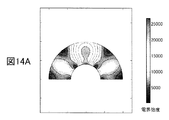
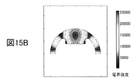
- FIG. 11 It is a figure which shows the result of calculation of the electric field strength distribution at the time of integrating plasma generation space and a processing chamber, and is a figure which shows the case of FIG. 11 with which plasma generation space and a processing chamber were integrated. It is a figure which shows the result of the calculation of the electric field strength distribution at the time of integrating a plasma generation space and a processing chamber, and the case where a dent of 2 cm depth is provided on the stage in FIG. 11 and a substrate is arranged on the dent.
- FIG. It is a figure which shows the result of the calculation of the electric field strength distribution at the time of integrating a plasma generation space and a processing chamber, and the case where a dent of 3 cm depth is provided on the stage in FIG.
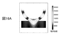
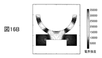
- FIG. It is a figure which shows the result of the calculation of the electric field strength distribution at the time of connecting a plasma generation space and a processing chamber, and is a figure which shows the case of FIG. 7 which connected a plasma generation space and a processing chamber. It is a figure which shows the result of the calculation of the electric field strength distribution at the time of connecting plasma generation space and a processing chamber, and shows the case where the clearance gap from the upper end of a chamber to the surface of a stage is set to 2.5 cm in FIG. FIG.
- FIG. 18 is a local cross-sectional view of the plasma processing apparatus of FIG. 17, showing a cross-sectional shape of a microwave introduction path formed between the processing chamber and the stage.
- FIG. 18 is a local cross-sectional view of the plasma processing apparatus of FIG. 17 and shows a cross-sectional shape of a waveguide.
- FIG. 17 It is a figure which shows schematically the structure of the 6th modification of the plasma processing apparatus in FIG. It is sectional drawing which shows roughly the structure of the plasma processing apparatus which concerns on the 5th Embodiment of this invention. It is a figure which shows schematically the structure of the 1st modification of the plasma processing apparatus in FIG. It is a figure which shows schematically the structure of the modification of the plasma processing apparatus in FIG. 22, and is a figure which shows the 2nd modification. It is a figure which shows roughly the structure of the modification of the plasma processing apparatus in FIG. 22, and is a figure which shows the 3rd modification. It is a figure which shows roughly the structure of the modification of the plasma processing apparatus in FIG. 17, and is a figure which shows the 7th modification.
- FIG. 17 It is a figure which shows roughly the structure of the modification of the plasma processing apparatus in FIG. 17, and is a figure which shows the 8th modification. It is a figure which shows the calculation result of the electric field strength distribution at the time of changing the height from the board
- FIG. It is a figure which shows the calculation result of the electric field strength distribution at the time of changing the height from the board
- FIG. 20A It is a figure which shows the calculation result of electric field strength distribution at the time of changing the height from the board
- FIG. 20A It is a figure which shows the calculation result of electric field strength distribution at the time of changing the length of the stub in the plasma processing apparatus of FIG. 20A, and is a figure which shows the case where the length of a stub is set to 1 cm.
- FIG. 21 When the distance of an opposing surface and a board
- FIG. It is a figure which shows the calculation result of electric field strength distribution at the time of changing the distance of the vertex of a cone-shaped inner wall surface, and a stage in the plasma processing apparatus of FIG. It is a figure which shows the case where it sets to. It is a figure which shows the calculation result of the electric field strength distribution at the time of changing the distance of the vertex of a cone-shaped inner wall surface and a stage in the plasma processing apparatus of FIG. 22, and sets the distance of the vertex of a cone-shaped inner wall surface and a stage to 10 cm.
- FIG. It is a figure which shows the calculation result of electric field strength distribution at the time of changing the distance of an opposing surface and a substrate mounting surface in the plasma processing apparatus of FIG.
- FIG. 23 shows the case where the distance of an opposing surface and a substrate mounting surface is set to 7 cm FIG. It is a figure which shows the calculation result of electric field strength distribution at the time of changing the distance of an opposing surface and a substrate mounting surface in the plasma processing apparatus of FIG. 23, and the case where the distance of an opposing surface and a substrate mounting surface is set to 6 cm FIG. It is a figure which shows the calculation result of electric field strength distribution at the time of changing the distance of an opposing surface and a substrate mounting surface in the plasma processing apparatus of FIG. 23, and when the distance of an opposing surface and a substrate mounting surface is set to 5 cm FIG. It is sectional drawing which shows roughly the structure of the plasma processing apparatus using a microwave.
- a plasma generating apparatus propagates a microwave, a spherical plasma generating chamber connected to the waveguide, a waveguide,
- a dielectric window interposed between the tube and the plasma generation chamber and introducing the microwave propagating through the waveguide into the plasma generation chamber
- a specific mode of electromagnetic waves can be excited, and a strong electric field region can be generated in an arbitrary region corresponding to the specific mode, so that the plasma is separated from the dielectric window and the desired region around the substrate to be processed
- the dielectric window can be prevented from being damaged by the plasma, and the plasma can be generated in a desired region around the substrate.
- the present invention has been made based on the results of the above research.
- FIG. 1 is a cross-sectional view schematically showing a configuration of a plasma processing apparatus including a plasma generation apparatus according to the first embodiment.
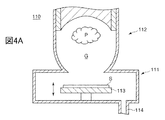
- the plasma processing apparatus 110 includes a processing chamber 111 (processing chamber) that performs plasma processing on the substrate S, and a plasma generation unit 112 (plasma generation apparatus) disposed adjacent to the processing chamber 111.
- a processing chamber 111 processing chamber
- a plasma generation unit 112 plasma generation apparatus
- the processing chamber 111 has a stage 113 on which the substrate S is placed, and an exhaust pipe 114 is connected thereto.
- the exhaust pipe 114 is connected to a vacuum pump and a pressure control valve (both not shown), and the vacuum pump and the pressure control valve control the pressure inside the processing chamber 111.
- the stage 113 has a heater and a cooling mechanism (both not shown) inside, and keeps the mounted substrate S at an appropriate temperature.
- the plasma generation unit 112 includes a waveguide 115 that propagates microwaves generated by a microwave generator (not shown), a plasma generation chamber 116 (plasma generation chamber) connected to the waveguide 115, and a waveguide. 115 and a dielectric window 117 interposed between the plasma generation chamber 116.
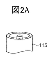
- the waveguide 115 is formed of a coaxial tube (see FIG. 2A) or a circular waveguide.
- microwaves having various dimensions of predetermined frequencies for example, microwaves of 2.45 GHz are the lowest order. It is set to be able to propagate in the mode.
- the plasma generation chamber 116 includes a cylindrical container 116a whose lower end in the figure is formed in a hemispherical shape, and a columnar member 116b whose lower end in the figure is formed in a hemispherical recess 116e.
- the cylindrical member 116b is coaxially accommodated inside the cylindrical container 116a, and the concave portion 116e at the lower end of the cylindrical member 116b and the inner wall surface 116d at the lower end of the cylindrical container 116a are formed into a spherical plasma generation space G (inside the plasma generation chamber).
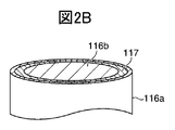
- a dielectric window 117 is disposed between the inner side surface of the cylindrical container 116a and the side surface of the columnar member 116b, and the gap between the upper inner wall surface of the cylindrical container 116a and the upper end of the columnar member 116b. (See, for example, FIG. 2B).
- a processing gas is introduced into the plasma generation space G from a processing gas inlet (not shown).
- a part of the lower end of the cylindrical container 116a is opened so that the plasma generation space G communicates with the inside of the processing chamber 111.
- a waveguide 115 is connected to the center of the upper surface of the cylindrical container 116a. That is, the waveguide 115 is disposed on the central axis of the cylindrical container 116a.
- the microwave propagating through the waveguide 115 is introduced into the plasma generation space G through the dielectric window 117.
- the dielectric window 117 faces the plasma generation space G along the outer periphery of the plasma generation space G, that is, faces the plasma generation space G symmetrically with respect to the central axis of the plasma generation space G.
- the wave is introduced symmetrically with respect to the central axis of the plasma generation space G.
- the plasma generation space G has a spherical shape, an electromagnetic wave of a specific mode can be excited by appropriately setting the radius thereof, and as a result, in an arbitrary region in the space, for example, above the center of the plasma generation space G A strong electric field region can be formed.
- the strong electric field region the amount of energy transferred from the microwave to the electrons in the plasma is large, so the electron temperature is high, and electrons with sufficient energy repeatedly collide with atoms and molecules in the process gas, resulting in high density.
- Plasma is generated locally. That is, in the strong electric field region, plasma is more actively generated than in other regions, so that the plasma P having a high density is generated in the region where the strong electric field is generated.
- the plasma P is generated from the processing gas in an arbitrary region only by introducing the microwave without using a magnetic field or the like.
- the plasma generation space G of the plasma generation chamber 116 and the inside of the processing chamber 111 communicate with each other, a part of the plasma P generated in the plasma generation space G is applied to the substrate S placed on the stage 113 of the processing chamber 111.
- the substrate S is subjected to plasma treatment.
- hydrogen gas, carbon-containing gas such as methane gas, propane gas or acetylene gas, and impurity-containing gas such as phosphine gas or diborane gas are used as the processing gas.
- the pressure in the plasma generation space G and the processing chamber 111 is maintained at 10 to 200 Torr.
- diamond is grown on the substrate S by radicals in the plasma P generated from the processing gas by heating the substrate S to 700 to 1200 ° C. by the stage 13.
- the plasma generation space G of the plasma generation chamber 116 into which microwaves are introduced has a spherical shape, electromagnetic waves of a specific mode can be excited by appropriately setting the radius.
- a strong electric field region can be generated in an arbitrary region corresponding to the specific mode, and thus the plasma P can be generated in a region away from the dielectric window 117.
- the dielectric window 117 can be prevented from being damaged by the plasma P.
- microwaves are introduced symmetrically with respect to the central axis of the plasma generation space G. Therefore, it becomes easy to set a radius necessary for exciting an electromagnetic wave of a specific mode and to predict a region where a strong electric field region is generated, so that the region of the generated plasma P can be easily controlled.
- a strong electric field region corresponding to the mode is generated in an arbitrary region by the plasma generation space G of the plasma processing apparatus 110.
- the main factor is that the inner wall surface 116d at the lower end of the cylindrical container 116a and the concave portion 116e at the lower end of the columnar member 116b have a hemispherical shape, which is a microwave boundary condition, and the electromagnetic wave excited by adjusting the radius thereof. It is considered that the mode can be specified. Therefore, it is sufficient that even the plasma generation space G has a spherical shape. For example, even if the microwave is introduced into the plasma generation space G symmetrically with respect to the central axis of the plasma generation space G, a strong local electric field is generated in an arbitrary region of the plasma generation space G. An area can be created.
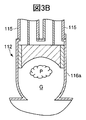
- one waveguide 115 may be arranged offset from the central axis of the cylindrical container 116a as shown in FIG. 3A, and a plurality of, for example, two conductors as shown in FIG. 3B.
- the wave tube 115 may be disposed offset from the central axis of the cylindrical container 116a.
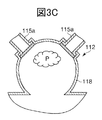
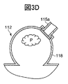
- a plasma generation unit 112 has a spherical plasma generation chamber 118 and a plurality of, for example, two, attached to the plasma generation chamber 118 to face the center of the plasma generation chamber 118 A waveguide 115a may be provided.
- the plasma generation unit 112 includes a spherical plasma generation chamber 118 and one waveguide 115a attached to the plasma generation chamber 118 so as to be directed to the center of the plasma generation chamber 118. You may prepare.
- the plasma generation chamber 118 has a spherical shape. Therefore, a strong local electric field region can be generated in an arbitrary region inside the plasma generation chamber 118.
- the waveguides 115 and 115a are symmetrically arranged with respect to the central axis of the cylindrical container 116a and the central axis of the plasma generation chamber 118. It is preferable to arrange. As a result, microwaves can be introduced symmetrically with respect to each central axis into the plasma generation space G and the plasma generation chamber 118, and the plasma P generation region can be easily controlled.
- the plasma processing apparatus 110 may be configured such that the stage 113 in the processing chamber 111 is movable in the vertical direction in the figure. Thereby, the distance between the plasma P and the substrate S can be controlled, and therefore, the film formation speed and the film thickness distribution on the substrate S can be controlled during film formation using the plasma P. Further, at the time of etching using the plasma P, the etching rate in the substrate S and the distribution of the etching rate can be controlled.
- the cylindrical container 116a is extended downward in the figure, so that the plasma generation space G is not a spherical shape, but is constituted by a cylindrical space and hemispherical spaces located above and below the cylindrical space. May be. Even in this case, the inner wall surface 116d at the lower end of the cylindrical container 116a and the concave portion 116e at the lower end of the columnar member 116b have a hemispherical shape.
- a strong electric field region can be generated in a specific region. As a result, a local strong electric field region can be generated in an arbitrary region in the plasma generation space G.
- the plasma generation space G is spherical, but the plasma generation space G is configured by a polyhedron shape approximating a spherical shape or a space shape formed by a curved surface represented by a higher-order function. Also good.
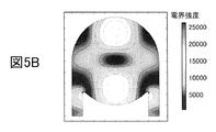
- Example 1 the radius of the plasma generation space G was set to 5.5 cm, and in Example 2, the radius of the plasma generation space G was set to 8 cm.
- a low-density plasma with a uniform distribution of n e 10 16 m ⁇ 3 that satisfies ⁇ > ⁇ pe already exists in the plasma generation space G ( ⁇ is a microwave (angular) frequency, and ⁇ pe is an electron plasma (angular) frequency, n e represents the electron density.), and the momentum transfer collision frequency ⁇ m is on the assumption that equal to omega, examples using an electromagnetic field calculation module manufactured by COMSOL Inc. 1 and example 2
- the electric field strength distribution in Fig. 5 was calculated, and the results are shown in Figs. 5A shows the electric field strength distribution in Example 1, and FIG. 5B shows the electric field strength distribution in Example 2.
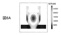
- Example 3 the stage 113 is not provided, and in Example 4, the distance from the stage 113 to the upper inner surface of the processing chamber 111 is set to 2 cm. In Example 5, the distance from the stage 113 to the upper inner surface of the processing chamber 111 was set to 1.5 cm.
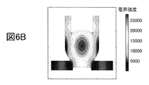
- FIGS. 6A to 6C show the electric field strength distribution in Examples 3 to 5 under the same conditions as in Examples 1 and 2, and the results are shown in FIGS. 6A to 6C.
- 6A shows the electric field strength distribution in Example 3
- FIG. 6B shows the electric field strength distribution in Example 4
- FIG. 6C shows the electric field strength distribution in Example 5.
- a local strong electric field region can be generated if the plasma generation space G has a spherical shape. I understood. This also suggests that the generation of the local strong electric field region is mainly caused by the shape of the plasma generation space G. It was also found that the local strong electric field region hardly changed even when the stage 113 was moved up and down. As a result, it is expected that a desired film forming rate and etching rate can be easily realized simply by moving the stage 113 up and down.
- the present inventors have a waveguide in which the plasma generation apparatus propagates microwaves, and a hemispherical curved space connected to the waveguide. If a plasma generation chamber and a dielectric window that is interposed between the waveguide and the plasma generation chamber and introduces the microwave propagating through the waveguide into the plasma generation chamber are provided, the boundary condition of the electromagnetic wave is obtained.
- electromagnetic waves of a specific mode can be excited, and a strong electric field region can be generated in an arbitrary region corresponding to the specific mode.
- the present invention has been made based on the results of the above research.
- FIG. 7 is a cross-sectional view schematically showing a configuration of a plasma processing apparatus provided with the plasma generation apparatus according to the second embodiment.
- the plasma processing apparatus 210 includes a processing chamber 211 (processing chamber) that performs plasma processing on the substrate S, and a plasma generation unit 212 (plasma generation apparatus) disposed adjacent to the processing chamber 211.
- the processing chamber 211 has a stage 213 on which the substrate S is placed, and an exhaust pipe 214 is connected thereto.
- the exhaust pipe 214 is connected to a vacuum pump and a pressure control valve (both not shown), and the vacuum pump and the pressure control valve control the pressure inside the processing chamber 211.
- the stage 213 includes a heater and a cooling mechanism (both not shown) inside, and controls the mounted substrate S so as to have an appropriate temperature.
- the plasma generation unit 212 includes a waveguide 215 that propagates microwaves generated by a microwave generator (not shown), a plasma generation chamber 216 (plasma generation chamber) connected to the waveguide 215, and a waveguide. 215 and a dielectric window 217 interposed between the plasma generation chamber 216.
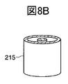
- the waveguide 215 includes a coaxial tube (see FIG. 8B) or a circular waveguide.
- microwaves having various dimensions of predetermined frequencies for example, microwaves of 2.45 GHz are the lowest order. It is set to be able to propagate in mode.
- the plasma generation chamber 216 is sandwiched between a cylindrical container 216 a having a hemispherical lower end in the drawing and a columnar member 216 b having a hemispherical convex portion 216 e having a lower end in the drawing. It has a hemispherical curved space. That is, the columnar member 216b is coaxially accommodated in the cylindrical container 216a, and a plasma generation space G (as a hemispherical curved space portion is formed by the convex portion 216e at the lower end of the cylindrical member 216b and the inner wall surface 216d at the lower end of the cylindrical container 216a. The inside of the plasma generation chamber) is formed. In addition, a dielectric window 217 is disposed in the gap between the inner side surface of the cylindrical container 216a and the side surface of the columnar member 216b (see, for example, FIG. 8A).
- the hemispherical curved space portion is concentrically opposed to the hemispherical curved surface (216e) and the hemispherical curved surface (216e) at a predetermined interval.
- a processing gas is introduced from a processing gas inlet (not shown) into the plasma generation space G as the plasma generation chamber 216.
- a part of the lower end of the cylindrical container 216a is opened so that the plasma generation space G communicates with the inside of the processing chamber 211.
- a waveguide 215 is connected to the center of the upper surface of the cylindrical container 216a. That is, the waveguide 215 is disposed on the central axis of the cylindrical container 216a.
- the microwave propagating through the waveguide 215 is introduced into the plasma introduction path 216c by the dielectric window 217, and the microwave introduced into the plasma introduction path 216c is further introduced into the plasma generation space G.
- the microwave introduction path 216 c is formed symmetrically with respect to the central axis of the plasma generation space G, the microwave is introduced symmetrically with respect to the central axis of the plasma generation space G.
- the plasma generation space G has a hemispherically curved space portion
- an electromagnetic wave of a specific mode can be excited by appropriately setting the inner and outer diameters of the hemispherically curved space portion, and as a result, an arbitrary region in the space, for example, A strong electric field region can be formed at the center of the plasma generation space G.
- the strong electric field region the amount of energy transfer from microwaves to electrons is large, so the electron temperature is high, and electrons with sufficient energy repeatedly collide with atoms and molecules in the processing gas, so that a high-density plasma is localized. Generated automatically.
- the plasma P is generated from the processing gas only by introducing the microwave without using a magnetic field or the like.
- the plasma processing apparatus 210 uses a mixed gas containing hydrogen gas, carbon-containing gas, for example, methane gas, propane gas, acetylene gas, and impurity-containing gas, for example, phosphine gas or diborane gas, as the processing gas.
- G and the pressure inside the processing chamber 211 are maintained at 10 to 200 Torr, and the substrate S is heated to 700 to 1200 ° C. by the stage 213, so that the radicals in the plasma P generated from the processing gas cause the diamond on the substrate S. Grow.
- the plasma processing apparatus 210 of FIG. 7 since the plasma generation space G as the plasma generation chamber 216 into which the microwave is introduced has the hemispherical curved space portion, the inner diameter and the outer diameter of the hemispherical curved space portion are set.
- an electromagnetic wave of a specific mode can be excited, a strong electric field region can be generated in an arbitrary region corresponding to the specific mode, and the plasma P can be generated in a region away from the dielectric window 217. Can be generated.
- the dielectric window 17 can be prevented from being damaged by the plasma P.
- the microwaves are introduced symmetrically with respect to the central axis of the plasma generation space G, the inner diameter and outer diameter of the hemispherical curved space necessary for exciting the electromagnetic wave of a specific mode are obtained. Appropriate setting and prediction of the region where the strong electric field region is generated can be facilitated, so that the region of the generated plasma P can be easily controlled.
- the inner wall surface 216d at the lower end of the cylindrical container 216a which is a microwave boundary condition, has a hemispherical shape, it is possible to specify the electromagnetic wave mode by the inner and outer diameters of the hemispherical curved space. It is considered that this is a main factor that a local strong electric field region corresponding to the mode is generated in the space G. Therefore, as long as the plasma generation space G has a hemispherical curved space portion, for example, the microwave is introduced into the plasma generation space G regardless of the form of microwave introduction. Even if it is not introduced symmetrically with respect to, a strong local electric field region can be generated in an arbitrary region of the plasma generation space G.
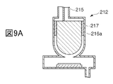
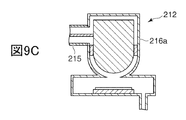
- one waveguide 215 may be disposed offset from the central axis of the cylindrical container 216a, and a plurality of, for example, two waveguides as shown in FIG. 9B. 215 may be arranged offset from the central axis of the cylindrical container 216a. Further, as shown in FIG. 9C, one waveguide 215 may be arranged on the side surface of the cylindrical container 216a.
- the plasma generation unit 212 shown in FIGS. 9A to 9C since the plasma generation space G has a hemispherical curved space portion, a substantially strong local electric field region is generated in an arbitrary region inside the plasma generation space G. Can do.
- the waveguides 215 are arranged symmetrically with respect to the central axis of the cylindrical container 216a. As a result, microwaves can be introduced symmetrically with respect to the central axis of the plasma generation space G, and the region of the generated plasma P can be easily controlled.
- the stage 213 in the processing chamber 211 may be configured to be movable in the vertical direction in the drawing as shown in FIG. 10A.
- the distance between the plasma P and the substrate S can be controlled, and therefore, the film formation speed and the film thickness distribution on the substrate S can be controlled during film formation using the plasma P.
- the etching rate in the substrate S and the distribution of the etching rate can be controlled at the time of etching using the plasma P.
- the inner volume of the plasma generation space G can be increased by expanding the space between the convex portion 216e at the lower end of the columnar member 216b and the inner wall surface 216d at the lower end of the cylindrical container 216a.
- the inner wall surface 216d at the lower end of the cylindrical container 216a has a hemispherical surface and these serve as boundary conditions, it is expected that a standing wave can be formed, and the shape of the hemispherical curved space portion is adjusted.
- a local strong electric field region can be generated in the plasma generation space G.
- FIG. 11 is a cross-sectional view schematically showing a configuration of a plasma processing apparatus including a plasma generation apparatus according to a third embodiment of the present invention.
- a processing chamber processing chamber for performing plasma processing on a substrate S and a plasma generation space G of the plasma generation apparatus are integrated.
- a plasma processing apparatus 220 has a cylindrical container 226a having a hemispherical upper end in the drawing, and an upper plane (stage) 226e in which the hemispherical convex portion at the upper end in the drawing is horizontally cut. And a cylindrical member 226b.
- the columnar member 226b is coaxially accommodated in the cylindrical container 226a, and a hemispherical space is formed between the stage 226e of the columnar member 226b and the inner wall surface 226d at the upper end of the cylindrical container 226a.
- This hemispherical space portion is an integration of a plasma generation space G consisting of a hemispherical curved space portion and a processing chamber 221 consisting of a hemispherical space portion corresponding to a convex portion cut out from the cylindrical member 226b. is there.
- a dielectric window 227 is disposed between the inner side surface of the cylindrical container 226a and the side surface of the columnar member 226b.
- a processing gas is introduced from a processing gas introduction port (not shown) into a plasma generation space G integrated with a processing chamber 221 for performing plasma processing.
- the cylindrical container 226a has an opening 226f at the center of the lower end, and a waveguide 225 is connected to the opening 226f.
- the microwave propagating through the waveguide 225 is introduced into the introduction path 226 c through the dielectric window 227, and the microwave introduced into the introduction path 226 c is further introduced into the plasma generation space G. Since the introduction path 226 c is arranged symmetrically with respect to the central axis of the plasma generation space G, the microwave is introduced symmetrically with respect to the center of the plasma generation space G.
- the plasma generation space G includes a hemispherical curved space portion
- an electromagnetic wave of a specific mode can be excited by appropriately setting the inner diameter and the outer diameter of the hemispherical curved space portion. For example, a local strong electric field region is generated in the center of the plasma generation space G.
- the plasma generation space G and the processing chamber 221 are integrated, a part of the plasma P generated in the plasma generation space G reaches the substrate S placed on the stage 226e of the processing chamber 221, As in the embodiment of FIG. 7, the substrate S is subjected to plasma treatment.
- the processing chamber (processing chamber) 221 for performing plasma processing on the substrate S and the plasma generation space G in the plasma generation apparatus are integrated, and the plasma generation space G is hemispherically curved. Since the space portion is provided, a strong electric field region can be generated in an arbitrary region of the plasma generation space G, and thus the plasma P can be generated in a region away from the dielectric window 227. As a result, the dielectric window 227 can be prevented from being damaged by the plasma P.
- FIG. 12A to FIG. 12C are diagrams showing modifications of the plasma processing apparatus according to the third embodiment.
- the arrangement of the waveguide 225 has a degree of freedom.
- one waveguide 225 is replaced with a cylindrical container 226a.
- a plurality of, for example, two waveguides 225 may be offset from the central axis of the cylindrical container 226a.
- one waveguide 225 may be disposed on the side surface of the cylindrical container 226a.
- the inner wall surface 226d at the upper end of the cylindrical container 226a is a hemispherical surface, they become electromagnetic wave boundary conditions, and as a result, a local strong electric field region can be generated in the plasma generation space G. it is conceivable that.
- Example 6 the cylindrical member 226b in the plasma processing apparatus 220 (see FIG. 11).
- the two-dimensional model of Example 6 and Example 7 is created assuming a plasma generation unit in which the upper end of the projection is convex and the stage 226e is not provided.
- the outer hemisphere in the plasma generation space G is created. The radius was set to 10 cm, the radius of the inner hemisphere was set to 4 cm, and in Example 7, the radius of the outer hemisphere in the plasma generation space G was set to 10 cm, and the radius of the inner hemisphere was set to 8 cm.
- a local strong electric field region can be generated. I understood. It has also been found that if the shape of the plasma generation space G is changed, the shape of the generated local strong electric field region is changed. Accordingly, it was inferred that the generation of the local strong electric field region is mainly caused by the shape of the plasma generation space G.
- FIG. 8 to 10 were created assuming the plasma processing apparatus 220 of FIG.
- a stage 226e is provided at the upper end of the cylindrical member 226b, and a recess is provided in the stage 226e in order to investigate the influence of the gap between the plasma P and the substrate S.
- the substrate S is mounted from the surface of the stage 226e. The depth to the bottom of the recess to be placed was set to 2 cm, and in Example 10, the depth from the surface of the stage 226e to the bottom of the recess to place the substrate S was set to 3 cm.
- FIGS. 15A to 15C show the electric field strength distribution in Example 8
- FIG. 15B shows the electric field strength distribution in Example 9
- FIG. 15C shows the electric field strength distribution in Example 10.
- Example 11 the processing chamber 211 (processing chamber) is connected to the outside (lower side in the figure) of the plasma generation space G in the plasma generation apparatus 210 (see FIG. 7).
- Examples 12 and 13 are In order to investigate the influence of the gap between the plasma P and the substrate S in the plasma processing apparatus of FIG. 7, the stage 213 of FIG. The interval was set to 2.5 cm, and in Example 13, the gap from the upper end of the chamber 211 to the surface of the stage 213 was set to 1.5 cm.
- FIGS. 16A to 16C show the electric field strength distribution in Example 11
- FIG. 16B shows the electric field strength distribution in Example 12
- FIG. 16C shows the electric field strength distribution in Example 13.
- a local strong electric field region can be generated. I understood that. This also suggests that the generation of the local strong electric field region is mainly caused by the shape of the plasma generation space G. It was also found that even if the stage 213 was moved up and down, the region of the local strong electric field region hardly changed. Thus, there is a possibility that a desired film formation rate and etching rate can be easily realized simply by moving the stage 213 up and down.
- the plasma processing apparatus includes a waveguide for propagating microwaves, a plasma generation chamber connected to the waveguide, A dielectric table disposed in the plasma generation chamber, interposed between the mounting table on which the substrate is mounted, and the waveguide and the plasma generation chamber, and introduces a microwave propagating through the waveguide into the plasma generation chamber.
- the plasma generation chamber has a central axis and exhibits a symmetrical shape with respect to the central axis, an electromagnetic wave of a specific mode can be obtained by appropriately setting the shape of the plasma generation chamber, for example, the inner diameter of a hemispherical shape.
- a strong electric field region can be generated in an arbitrary region corresponding to the specific mode, so that the plasma is separated from the dielectric window, and a desired region around the substrate to be processed can be obtained.
- Generate in region Bets can be, as a result, found that it is possible that it is possible to prevent the dielectric window is damaged by the plasma, to generate a plasma in a desired region of the periphery of the substrate.
- the present invention has been made based on the results of the above research.
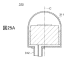
- FIG. 17 is a cross-sectional view schematically showing the configuration of the plasma processing apparatus according to the present embodiment.
- the plasma processing apparatus 310 includes a processing chamber 311 (plasma generation chamber) for performing plasma processing on the substrate S, and a waveguide 312 for propagating microwaves generated by a microwave generator (not shown).
- a processing chamber 311 plasma generation chamber
- a waveguide 312 for propagating microwaves generated by a microwave generator (not shown).
- the processing chamber 311 includes therein a stage 314 for placing the substrate S on the substrate placement surface 314a, and is connected to an exhaust pipe (not shown).
- the exhaust pipe is connected to a vacuum pump and a pressure control valve (both not shown), and the vacuum pump and the pressure control valve control the pressure inside the processing chamber 311.
- the stage 314 has a heater and a cooling mechanism (both not shown) inside, and controls the placed substrate S to an appropriate temperature.
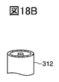
- a coaxial tube or a circular waveguide is used as the waveguide 312.
- microwaves having various dimensions, for example, microwaves of 2.45 GHz can be propagated in the lowest mode. Is set to
- the processing chamber 311 has a central axis C and has a symmetrical shape with respect to the central axis C.
- the upper end side in the figure is formed in a hemispherical shape, and the lower end side in the figure is formed in a cylindrical shape.
- the stage 314 has a cylindrical shape and is disposed coaxially with the processing chamber 311 inside the processing chamber 311.
- the hemispherical inner wall surface 311a of the processing chamber 311 and the substrate placement surface 314a of the stage 314 form a plasma generation space G.
- a processing gas is introduced into the plasma generation space G from a processing gas introduction port (not shown).
- a dielectric window 315 is disposed between the inner wall surface of the processing chamber 311 and the side surface of the stage 314 (see, for example, FIG. 18A).
- a waveguide 312 is connected to the processing chamber 311 at the center at the lower end in the figure. That is, the waveguide 312 is disposed on the central axis C of the processing chamber 311.
- the microwave propagating through the waveguide 312 is introduced into the plasma generation space G through the dielectric window 315.
- the dielectric window 315 faces the plasma generation space G along the outer periphery of the plasma generation space G, that is, faces the plasma generation space G symmetrically with respect to the central axis C, so that the microwaves generate plasma. It is introduced symmetrically with respect to the center of the space G.
- the plasma generation space G is formed by the hemispherical inner wall surface 311a of the processing chamber 311 and the substrate placement surface 314a of the stage 314, it exhibits a symmetrical hemispherical shape with respect to the central axis C.
- an electromagnetic wave of a specific mode can be excited by appropriately setting the radius, and as a result, a strong electric field region can be formed in an arbitrary region in the space, for example, above the center of the plasma generation space G.
- the strong electric field region the amount of energy transferred from the microwave to the electrons in the plasma is large, so the electron temperature is high, and electrons with sufficient energy repeatedly collide with atoms and molecules in the process gas, resulting in high density. Plasma is generated locally.
- plasma is more actively generated in the strong electric field region than in the other regions, and thus the plasma P having a high density is generated in the strong electric field region.
- the plasma P is generated from the processing gas in an arbitrary region only by introducing the microwave without using a magnetic field or the like.
- the plasma processing apparatus 310 uses a mixed gas containing hydrogen gas, carbon-containing gas such as methane gas, propane gas or acetylene gas, and impurity-containing gas such as phosphine gas or diborane gas as the processing gas, G and the internal pressure of the processing chamber 311 are maintained at 10 to 200 Torr, and the substrate S is heated to 700 to 1200 ° C. by the stage 314, whereby diamond is generated on the substrate S by radicals in the plasma P generated from the processing gas. Grow.
- the upper end side of the processing chamber 311 into which microwaves are introduced has a hemispherical shape symmetric with respect to the central axis C, and the plasma generation space G in the processing chamber 311 is also symmetric with respect to the central axis C. Since it exhibits a hemispherical shape, an electromagnetic wave of a specific mode can be excited by appropriately setting the radius thereof, and a strong electric field region can be generated in an arbitrary region corresponding to the specific mode. It can be generated in a region away from the dielectric window 315. As a result, the dielectric window 315 can be prevented from being damaged by the heat of the plasma P.
- the potential gradient in the sheath near the surface of the dielectric window 315 can be weakened, so that the positive potential to the dielectric window 315 by the sheath can be reduced. Sputtering of ions or the like can be weakened.
- the plasma generation space G has a hemispherical shape that is symmetric with respect to the central axis C, the generated plasma P is also distributed symmetrically with respect to the central axis C. Thereby, generation
- the microwaves are introduced symmetrically with respect to the central axis C of the processing chamber 311, the setting of the radius necessary for exciting the electromagnetic wave of the specific mode and the position where the strong electric field region is generated. Prediction becomes easy, so that the generation region of the plasma P can be easily controlled.
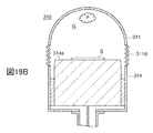
- a part of the substrate mounting surface 314a in the stage 314 in the processing chamber 311 may be configured as a lift table 314c that can move in the vertical direction in the drawing as shown in FIG. 19A. Thereby, the distance between the plasma P and the substrate S can be controlled.
- a part of the side wall of the processing chamber 311 may be constituted by a bellows 311d.
- the bellows 311d by extending the bellows 311d, the distance between the upper end side of the processing chamber 311 having the hemispherical shape and the substrate S placed on the stage 314 can be changed, but the strong electric field region is the hemisphere of the processing chamber 311. As a result, the distance between the plasma P and the substrate S can be controlled.
- the film formation speed and the film thickness distribution on the substrate S are controlled during the film formation using the plasma P by controlling the distance between the plasma P and the substrate S.
- the etching rate in the substrate S and the distribution of the etching rate can be controlled.
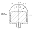
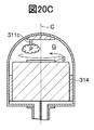
- a protrusion member (stub) 311c facing the stage 314 along the central axis C may be provided on the hemispherical inner wall surface 311a of the processing chamber 311.
- a protrusion member (stub) 311c facing the stage 314 along the central axis C may be provided on the hemispherical inner wall surface 311a of the processing chamber 311.
- plasma is generated locally near the tip of the protrusion. Therefore, by adjusting the length of the stub 311c, the generation region of the plasma P in the plasma generation space G can be controlled more precisely in the vertical direction.
- the material constituting the stub 311c is not particularly limited. For example, a metal is preferable.
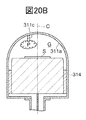
- the stub 311c is not necessarily arranged along the central axis C, and may be offset from the central axis C as shown in FIG. 20B. Even if the stub 311c is offset from the central axis C, the plasma P can be locally generated in the vicinity of the tip as long as the tip of the stub 311c exists in the plasma generation space G. Accordingly, the generation location of the plasma P can be controlled by adjusting the arrangement location of the stub 311c.
- the stub 311c may be configured to be movable in the plasma generation space G.
- it may be configured to be capable of circular movement about the central axis C while facing the stage 314.
- the plasma P since the plasma P is locally generated near the tip of the stub 311c, the plasma P can be moved by moving the stub 311c.
- the exposure time to the plasma P at various locations on the substrate S can be controlled, so that uniform plasma treatment can be performed on the substrate S.
- a portion facing the stage 314 on the upper end side of the processing chamber 311 may be cut out to provide a flat opposing surface 311e on the hemispherical inner wall surface 311a.
- a curved surface portion remains in a part of the hemispherical inner wall surface 311a, an electromagnetic wave of a specific mode can be excited by appropriately setting the radius of the curved surface portion, and according to the specific mode.
- the facing surface 311e is closer to the substrate placement surface 314a of the stage 314 than the top of the hemispherical inner wall surface 311a in FIG. It is possible to approach the substrate S placed on the placement surface 314a, so that the efficiency of the plasma treatment performed on the substrate S can be improved.
- FIG. 22 is a cross-sectional view schematically showing the configuration of the plasma processing apparatus according to the present embodiment.
- the plasma processing apparatus 360 includes a processing chamber 361 (plasma generating chamber) that performs plasma processing on the substrate S, and a waveguide 312.
- the processing chamber 361 has a central axis C1, has a symmetrical shape with respect to the central axis C1, and has an upper end side formed in a conical shape in the drawing and a lower end side formed in a cylindrical shape in the drawing.
- the stage 314 is disposed coaxially with the processing chamber 361 inside the processing chamber 361.
- the conical inner wall surface 361a on the upper end side of the processing chamber 361 and the substrate placement surface 314a of the stage 314 form a plasma generation space G1.
- a waveguide 312 is connected to the processing chamber 361 at the center at the lower end in the figure. That is, the waveguide 312 is disposed on the central axis C1 of the processing chamber 361.
- the microwave is introduced symmetrically with respect to the center of the plasma generation space G1 through the dielectric window 315.
- the plasma generation space G1 is formed by the conical inner wall surface 361a of the processing chamber 361 and the substrate placement surface 314a of the stage 314, the plasma generation space G1 has a symmetrical conical shape with respect to the central axis C1.
- An electromagnetic wave of a specific mode can be excited by appropriately setting the position of the conical surface in the conical shape, and an arbitrary region corresponding to the specific mode, for example, a local strong electric field region above the plasma generation space G1 To generate plasma P1.
- a part of the plasma P1 generated in the plasma generation space G1 reaches the substrate S placed on the substrate placement surface 314a facing the plasma generation space G1, and plasma treatment is performed on the substrate S.
- the upper end side of the processing chamber 361 into which microwaves are introduced has a conical shape symmetrical with respect to the central axis C1, and the plasma generation space G1 in the processing chamber 361 is also symmetrical with respect to the central axis C1. Since it exhibits a conical shape, it is possible to excite an electromagnetic wave of a specific mode by appropriately setting the position of the conical surface in the conical shape, and to generate a strong electric field region in an arbitrary region according to the specific mode. Thus, the plasma P1 can be generated in a region away from the dielectric window 315. Furthermore, the potential gradient in the sheath generated in the vicinity of the surface of the dielectric window 315 can be weakened, so that the sputtering of cations or the like on the dielectric window 315 by the sheath can be weakened.
- the plasma generation space G1 has a conical shape which is symmetric with respect to the central axis C1
- the generated plasma P1 is also distributed symmetrically with respect to the central axis C1.
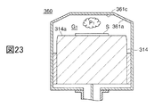
- a portion facing the stage 314 on the upper end side of the processing chamber 361 may be cut out to provide a flat opposing surface 361c on the conical inner wall surface 361a.
- the inclined surface remains in part on the conical inner wall surface 361a, an electromagnetic wave of a specific mode can be excited by appropriately setting the position of the inclined surface, and an arbitrary mode corresponding to the mode can be excited.
- the plasma P1 can be generated in the region of FIG. 22, the opposing surface 361c is closer to the substrate mounting surface 314a of the stage 314 than the top of the conical inner wall surface 361a in FIG. It can be brought close to the substrate S placed on the surface 314a, and thus the efficiency of the plasma treatment performed on the substrate S can be improved.
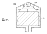
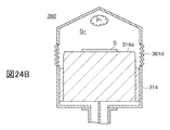
- a part of the substrate mounting surface 314a on the stage 314 in the processing chamber 361 may be configured as a lift table 314c movable in the vertical direction in the drawing as shown in FIG. 24A. Thereby, the distance between the plasma P1 and the substrate S can be controlled.
- a part of the side wall of the processing chamber 361 may be constituted by a bellows 361d. Also in this case, the distance between the plasma P1 and the substrate S can be controlled by extending the bellows 361d.
- a stub facing the stage 314 along the central axis C1 may be provided on the conical inner wall surface 361a in the processing chamber 361 of the plasma processing apparatus 360.
- the main factor that the strong electric field region corresponding to the mode is generated in an arbitrary region in the plasma generation spaces G and G1 of the plasma processing apparatuses 310 and 360 is as follows.
- the upper end side of the processing chamber 311 having the hemispherical inner wall surface 311a and the upper end side of the processing chamber 361 having the conical inner wall surface 361a are symmetrical with respect to the central axis C and the central axis C1, and are excited by adjusting the shape. It is considered that the electromagnetic wave mode to be specified can be specified.
- the microwave is symmetrical with respect to the center of the plasma generation space G regardless of the form of microwave introduction to the plasma generation space G. Even if it is not introduced into the region, a strong local electric field region can be generated in an arbitrary region of the plasma generation space G.
- the waveguide 312 may be arranged offset from the central axis C of the processing chamber 311. Further, the microwave does not need to be introduced into the plasma generation space G through the dielectric window 315.
- the waveguide 312 may be directly attached to the upper end side of the processing chamber 311.
- the height of the lift table 314c from the substrate placement surface 314a is set to 0 cm.
- the height of the lift table 314c from the substrate placement surface 314a is set to 2 cm.
- the height of the lift table 314c from the substrate placement surface 314a was set to 3 cm.
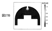
- Example 17 the length of the stub 311c was set to 1 cm
- Example 18 the length of the stub 311c was set to 2 cm
- Example 19 the length of the stub 311c was set to 3 cm.
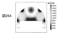
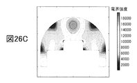
- FIG. 27A to FIG. 27C calculate the electric field strength distributions in Examples 17 to 19 using the same COMSOL electromagnetic field calculation module under the same conditions as in Examples 14 to 16, and the results. Is shown. 27A shows the electric field strength distribution in Example 17, FIG. 27B shows the electric field strength distribution in Example 18, and FIG. 27C shows the electric field strength distribution in Example 19.
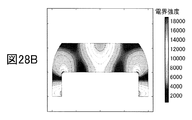
- Example 20 to Example 22 The two-dimensional model of Example 20 to Example 22 is created assuming 310, the distance between the facing surface 311e and the substrate mounting surface 314a is set to 7 cm in Example 20, and the facing surface 311e is set in Example 21. The distance from the substrate placement surface 314a was set to 6 cm, and in Example 22, the distance between the facing surface 311e and the substrate placement surface 314a was set to 5 cm.
- FIGS. 28A to 28C show the electric field strength distributions in Examples 20 to 22 using the same COMSOL electromagnetic field calculation module under the same conditions as in Examples 14 to 16, and the results. Is shown. 28A shows the electric field strength distribution in Example 20, FIG. 28B shows the electric field strength distribution in Example 21, and FIG. 28C shows the electric field strength distribution in Example 22.
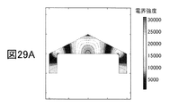
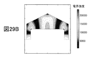
- Example 23 the distance between the apex of the conical inner wall surface 361a and the stage 314 is set to 5 cm, and in Example 24, the distance between the apex of the conical inner wall surface 361a and the stage 314 is set to 7.5 cm. 25, the distance between the apex of the conical inner wall surface 361a and the stage 314 was set to 10 cm.
- FIGS. 29A to 29C show the electric field strength distributions in Examples 23 to 25 using the same COMSOL electromagnetic field calculation module under the same conditions as in Examples 14 to 16, and the results. Is shown. 29A shows the electric field strength distribution in Example 23, FIG. 29B shows the electric field strength distribution in Example 24, and FIG. 29C shows the electric field strength distribution in Example 25.
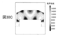
- the plasma processing apparatus of FIG. 360 the two-dimensional model of Example 26 thru
- the distance from the substrate placement surface 314a was set to 6 cm, and in Example 28, the distance between the facing surface 361c and the substrate placement surface 314a was set to 5 cm.
- FIG. 30A to FIG. 30C show the electric field strength distributions in Examples 26 to 28 using the same COMSOL electromagnetic field calculation module under the same conditions as in Examples 14 to 16, and the results. Is shown. 30A shows the electric field strength distribution in Example 26, FIG. 30B shows the electric field strength distribution in Example 27, and FIG. 30C shows the electric field strength distribution in Example 28.
- FIGS. 30A to 30C it was found that a strong electric field region was locally generated even when the facing surface 361c was provided. As a result, it was found that if the inclined surface remains in part on the conical inner wall surface 361a, the plasma P1 can be generated in the plasma generation space G1 even if the upper end side of the processing chamber 361 does not exhibit a complete conical shape. Further, it was found that the strong electric field region is generated in the vicinity of the opposing surface 361c even if the distance between the opposing surface 361c and the substrate mounting surface 314a is changed. Thereby, it was also found that the distance between the plasma P1 and the substrate S can be controlled by changing the distance between the facing surface 361c and the substrate placement surface 314a.
Landscapes
- Physics & Mathematics (AREA)
- Engineering & Computer Science (AREA)
- Plasma & Fusion (AREA)
- Chemical & Material Sciences (AREA)
- Analytical Chemistry (AREA)
- Plasma Technology (AREA)
Abstract
マイクロ波を導入するための誘電体窓が損傷するのを防止することができるプラズマ処理装置を提供する。プラズマ処理装置110は、基板Sを収容する処理チャンバ111と、該処理チャンバ111に隣接して配置されるプラズマ生成ユニット112とを備え、該プラズマ生成ユニット112は、マイクロ波を伝播させる導波管115と、該導波管115に接続されたプラズマ生成チャンバ116と、導波管115及びプラズマ生成チャンバ116の間に介在し、導波管115が伝播するマイクロ波をプラズマ生成チャンバ116の内部へ導入する誘電体窓117とを有し、プラズマ生成チャンバ116の内部空間であるプラズマ発生空間Gは球状を呈し、処理チャンバ111の内部と連通する。
Description
本発明は、マイクロ波を用いてプラズマを生成するプラズマ生成装置及びプラズマ処理装置に関する。
従来、処理ガスからプラズマを生成し、該プラズマによって基板に処理を施す数々のプラズマ処理装置が用いられている。例えば、平行に配置された2つの平板状電極に高周波電力を供給することによって高周波電界を生じさせ、該電界によって加速された電子と処理ガスとが様々な反応を起こすことでプラズマを生成し、該プラズマによって基板へプラズマ処理を施す平行平板型のプラズマ処理装置が一般に用いられている。また、高周波ではなくマイクロ波を用いるプラズマ処理装置も用いられている。
図31は、マイクロ波を用いるプラズマ処理装置の構成を概略的に示す断面図である。
図31において、プラズマ処理装置450は、マイクロ波を導入するための開口部451を上部中心に有する真空チャンバ452と、該真空チャンバ452の内部に配置されて基板Sを載置する基板載置台453と、開口部451へマイクロ波を導入する導波管454と、該導波管454から真空チャンバ452の内部へマイクロ波を導入する誘電体窓455とを備える。
このプラズマ処理装置450では、真空チャンバ452の内部へ導入された処理ガスからマイクロ波によってプラズマが生成され、該プラズマ中のラジカルによって基板載置台453上の基板Sにおいて、例えば、ダイヤモンドを成長させる(例えば、特許文献1参照)。
真空チャンバ452の内部においてプラズマの電子密度が高まると、プラズマは誘電体窓455を透過したマイクロ波を遮断するようになる。これに加えて、高密度の不均一なプラズマ中では、電子プラズマ(角)周波数とマイクロ波周波数が一致する位置で、共鳴吸収が起こる。その結果、誘電体窓455の近傍において積極的にプラズマが生成される。比較的圧力の高い条件下でプラズマを生成すると処理ガスの温度が非常に高温となり、誘電体窓455を熱によって損傷させる場合があり、又、被処理体である基板S周辺に所望のプラズマを生成することができなくなる場合がある。
本発明の目的は、マイクロ波を導入するための誘電体窓が損傷するのを防止し、且つ基板周辺の所望の領域にプラズマを生成することができるプラズマ生成装置及びプラズマ処理装置を提供することにある。
上記目的を達成するために、本発明の第1の態様によれば、マイクロ波を伝播させる導波管と、該導波管に接続されたプラズマ生成室と、前記導波管及び前記プラズマ生成室の間に介在し、前記導波管が伝播する前記マイクロ波を前記プラズマ生成室の内部へ導入する誘電体窓とを備えることを特徴とするプラズマ生成装置が提供される。
本発明の第1の態様において、前記プラズマ生成室は、球状(球状に近似する多面体形状や高次の関数によって表される曲面で形成される空間形状を含む。)を呈し、基板を収容する処理室に隣接して配置され、前記プラズマ生成室の内部は前記処理室の内部と連通することが好ましい。
本発明の第1の態様において、前記導波管は前記プラズマ生成室の中心軸に関して対称的に配置されることが好ましい。
本発明の第1の態様において、前記プラズマ生成室は、半球体状の湾曲表面と、該半球体状の湾曲表面とは所定の間隔を隔てて、同心状に対向配置された前記半球体状の径よりも径が大きい中空半球体状の内側湾曲面とによって挟まれた半球状湾曲空間部を備えていることが好ましい。
本発明の第1の態様において、前記プラズマ生成室は基板を収容する処理室に隣接して配置され、前記プラズマ生成室の内部は前記処理室の内部と連通していることが好ましい。
本発明の第1の態様において、前記導波管は前記プラズマ生成室の中心軸に関して対称的に配置されていることが好ましい。
上記目的を達成するために、本発明の第2の態様によれば、マイクロ波を伝播させる導波管と、該導波管に接続されるプラズマ生成室と、該プラズマ生成室内に配され、基板を載置する載置台と、前記導波管及び前記プラズマ生成室の間に介在し、前記導波管を伝播する前記マイクロ波を前記プラズマ生成室の内部へ導入する誘電体窓とを備え、前記プラズマ生成室は中心軸を有し、該中心軸に関して対称な形状を呈することを特徴とするプラズマ処理装置が提供される。
本発明の第2の態様において、前記プラズマ生成室は半球形状を呈することが好ましい。
本発明の第2の態様において、前記プラズマ生成室は前記載置台と対向する部分が切除されていることが好ましい。
本発明の第2の態様において、前記プラズマ生成室は円錐形状を呈することが好ましい。
本発明の第2の態様において、前記プラズマ生成室は前記載置台と対向する部分が切除されていることが好ましい。
本発明の第2の態様において、前記プラズマ生成室に前記載置台と対向する突起部材が配置されていることが好ましい。
本発明の第2の態様において、前記突起部材は前記プラズマ生成室の中心軸からオフセットして配置されていることが好ましい。
本発明の第2の態様において、前記突起部材は移動可能に構成されていることが好ましい。
上記目的を達成するために、本発明の第3の態様によれば、基板を収容する処理室と、該処理室に隣接して配置されるプラズマ生成装置とを備え、該プラズマ生成装置は、マイクロ波を伝播させる導波管と、該導波管に接続されたプラズマ生成室と、前記導波管及び前記プラズマ生成室の間に介在し、前記導波管が伝播する前記マイクロ波を前記プラズマ生成室の内部へ導入する誘電体窓とを有し、前記プラズマ生成室の内部は前記処理室の内部と連通することを特徴とするプラズマ処理装置が提供される。
本発明の第3の態様において、前記プラズマ生成室は、球状を呈していることが好ましい。
本発明の第3の態様において、前記プラズマ生成室は、半球体状の湾曲表面と、該半球体状の湾曲表面とは所定の間隔を隔てて同心状に対向配置された前記半球体状の径よりも径が大きい中空半球体状の内側湾曲面とによって挟まれた半球状湾曲空間部を備えていることが好ましい。
本発明によれば、マイクロ波が導入されるプラズマ生成室が球状を呈するので、プラズマ生成室内に存在する電磁波の境界条件となるプラズマ生成室の半径を適切に設定することにより、特定のモードの電磁波を励起できる。その結果、モードに応じた任意の領域において強電界領域を生じさせることができる。強電界領域は処理ガスからプラズマを生成する。したがって、誘電体窓から離れ且つ被処理体である基板周辺の所望の領域において強電界領域を生じさせることにより、プラズマを誘電体窓から離れた領域において生成することができ、もって、誘電体窓がプラズマによって損傷するのを防止することができるとともに、基板周辺の所望の領域にプラズマを生成することができる。
また、本発明によれば、マイクロ波が導入されるプラズマ生成室が、半球体状の湾曲表面と、該半球体状の湾曲表面とは所定の間隔を隔てて、同心状に対向配置された半球体状の径よりも径が大きい中空半球体状の内側湾曲面とによって挟まれた半球状湾曲空間部を備えているので、電磁波の境界条件となる半球状湾曲空間部の内径及び外径を適切に設定することで、特定のモードの電磁波を励起できる。その結果、モードに応じた任意の領域で強電界領域を生じさせることができる。強電界領域は処理ガスからプラズマを生成する。したがって、誘電体窓から離れ且つ被処理体である基板周辺の所望の領域において強電界領域を生じさせることにより、プラズマを誘電体窓から離れた領域で生成することができ、もって、誘電体窓がプラズマによって損傷するのを防止することができ、更に基板周辺の所望の領域にプラズマを生成することができる。
また、本発明によれば、マイクロ波が導入されるプラズマ生成室が中心軸に関して対称な形状を呈するので、プラズマ生成室内に存在する電磁波の境界条件となるプラズマ生成室の形状、例えば、半球形状の内径を適切に設定することにより、特定のモードの電磁波を励起できる。その結果、モードに応じた任意の領域において強電界領域を生じさせることができる。強電界領域は処理ガスからプラズマを生成する。したがって、誘電体窓から離れ且つ被処理体である基板周辺の所望の領域において強電界領域を生じさせることにより、プラズマを誘電体窓から離れた領域において生成することができ、もって、誘電体窓がプラズマによって損傷するのを防止することができるとともに、基板周辺の所望の領域にプラズマを生成することができる。
本発明者等は、上記目的を達成すべく鋭意研究を行った結果、プラズマ生成装置がマイクロ波を伝播させる導波管と、該導波管に接続された球状のプラズマ生成室と、導波管及びプラズマ生成室の間に介在し、導波管が伝播するマイクロ波をプラズマ生成室の内部へ導入する誘電体窓とを備えれば、プラズマ生成室の半径を適切に設定することで、特定のモードの電磁波を励起でき、該特定モードに応じた任意の領域において強電界領域を生じさせることができ、もって、プラズマを誘電体窓から離し且つ被処理体である基板周辺の所望の領域において生成することができ、その結果、誘電体窓がプラズマによって損傷するのを防止することができるとともに、基板周辺の所望の領域にプラズマを生成することができることを見出した。
本発明は、上記研究の結果に基づいてなされたものである。
以下、本発明の第1の実施の形態について図面を参照しながら説明する。
図1は、第1の本実施の形態に係るプラズマ生成装置を備えるプラズマ処理装置の構成を概略的に示す断面図である。
図1において、プラズマ処理装置110は、基板Sにプラズマ処理を施す処理チャンバ111(処理室)と、該処理チャンバ111に隣接して配置されるプラズマ生成ユニット112(プラズマ生成装置)とを備える。
処理チャンバ111は、基板Sを載置するステージ113を内部に有し、排気管114が連結される。排気管114は真空ポンプや圧力制御バルブ(ともに図示しない)に接続され、真空ポンプや圧力制御バルブは処理チャンバ111の内部の圧力を制御する。ステージ113は内部にヒータや冷却機構(ともに図示しない)を有し、載置された基板Sを適切な温度に保つ。
プラズマ生成ユニット112は、マイクロ波ジェネレータ(図示しない)が発生させるマイクロ波を伝播させる導波管115と、該導波管115に接続されたプラズマ生成チャンバ116(プラズマ生成室)と、導波管115及びプラズマ生成チャンバ116の間に介在する誘電体窓117とを有する。
導波管115は、同軸管(図2A参照)、若しくは円形導波管からなり、円形導波管の場合、諸寸法が所定の周波数のマイクロ波、例えば、2.45GHzのマイクロ波を最低次のモードにおいて伝播できるように設定されている。
プラズマ生成チャンバ116は図中における下端が半球状に形成された円筒容器116aと、図中における下端が半球状の凹部116eに形成された円柱部材116bとを有する。円柱部材116bは円筒容器116aの内部に同軸に収容され、円柱部材116bの下端の凹部116eと、円筒容器116aの下端の内壁面116dとは、球状のプラズマ発生空間G(プラズマ生成室の内部)を形成する。また、円筒容器116aの内側面、及び円柱部材116bの側面の間、並びに、円筒容器116aの上端の内壁面、及び円柱部材116bの上端の間の隙間には、誘電体窓117が配される(例えば、図2B参照)。
プラズマ生成チャンバ116では、プラズマ発生空間Gへ図示しない処理ガス導入口から処理ガスが導入される。また、円筒容器116aの下端の一部が、開放されてプラズマ発生空間Gと処理チャンバ111の内部とが連通する。さらに、円筒容器116aの上面中心には導波管115が接続される。すなわち、導波管115は円筒容器116aの中心軸上に配置される。
プラズマ生成ユニット112では、導波管115を伝播するマイクロ波が誘電体窓117によってプラズマ発生空間Gへ導入される。ここで、誘電体窓117はプラズマ発生空間Gの外周に沿って該プラズマ発生空間Gに面する、すなわち、プラズマ発生空間Gの中心軸に関して対称的に該プラズマ発生空間Gに面するので、マイクロ波はプラズマ発生空間Gの中心軸に関して対称的に導入される。
また、プラズマ発生空間Gは球状を呈するので、その半径を適切に設定することによって特定のモードの電磁波を励起でき、結果として空間中の任意の領域、例えば、プラズマ発生空間Gの中心の上方において、強電界領域を形成できる。当該強電界領域では、マイクロ波からプラズマ中の電子へのエネルギー移行量が大きいために電子温度が高くなり、十分なエネルギーを持つ電子が処理ガス中の原子や分子と衝突を繰り返すことで高密度のプラズマが局所的に生成される。すなわち、強電界領域では他の領域よりもプラズマの生成が積極的に起こるため、強電界が生じた領域では密度の高いプラズマPが生じる。換言すれば、本実施の形態では磁界等を利用することなく、マイクロ波の導入のみによって、処理ガスからプラズマPを任意の領域において生じさせる。
ここで、プラズマ生成チャンバ116のプラズマ発生空間Gと処理チャンバ111の内部は連通するため、プラズマ発生空間Gにおいて生じたプラズマPの一部は処理チャンバ111のステージ113に載置された基板Sに到達し、該基板Sにプラズマ処理を施す。例えば、プラズマ処理装置110では、処理ガスとして、水素ガス、炭素含有ガス、例えば、メタンガス、プロパンガスやアセチレンガス、及び不純物含有ガス、例えば、ホスフィンガスやジボランガスを含む混合ガスを用いる。例えば、プラズマ処理装置110では、プラズマ発生空間Gや処理チャンバ111の内部の圧力を10~200Torrに維持する。例えば、プラズマ処理装置110では、基板Sをステージ13によって700~1200℃に加熱することにより、処理ガスから生じたプラズマP中のラジカルによって基板S上でダイヤモンドを成長させる。
図1のプラズマ処理装置110によれば、マイクロ波が導入されるプラズマ生成チャンバ116のプラズマ発生空間Gが球状を呈するので、その半径を適切に設定することによって特定のモードの電磁波を励起できる。該特定のモードに応じた任意の領域において強電界領域を生じさせることができ、もって、プラズマPを誘電体窓117から離れた領域において生成することができる。その結果、誘電体窓117がプラズマPによって損傷するのを防止することができる。
プラズマ処理装置110では、マイクロ波がプラズマ発生空間Gの中心軸に関して対称的に導入される。よって、特定のモードの電磁波を、励起するために必要な半径の設定、及び強電界領域が生じる領域の予測が容易となり、もって、生成されるプラズマPの領域を容易に制御することができる。
本実施の形態において、プラズマ処理装置110のプラズマ発生空間Gによって、モードに応じた強電界領域が任意の領域において生じる。その主要因は、マイクロ波の境界条件となる、円筒容器116aの下端の内壁面116dや、円柱部材116bの下端の凹部116eが半球状を呈し、その半径を調整することによって励起される電磁波のモードを特定できることにあると考えられる。したがって、プラズマ発生空間Gさえ球状を呈していればよい。プラズマ発生空間Gに対するマイクロ波の導入形態が、例えば、マイクロ波がプラズマ発生空間Gの中心軸に関して対称的に導入されていなくとも、プラズマ発生空間Gの任意の領域において、概ね局所的な強電界領域を生じさせることができる。
以上の理由から、導波管115の配置には自由度があり、図1のプラズマ処理装置110のように、導波管115を円筒容器116aの中心軸上に配置する必要はない。例えば、1つの導波管115は、図3Aに示すように、円筒容器116aの中心軸からオフセットして配置してもよく、また、図3Bに示すように、複数の、例えば、2つの導波管115を円筒容器116aの中心軸からオフセットして配置してもよい。
さらに、マイクロ波は、必ずしも誘電体窓117を経てプラズマ発生空間Gへ導入する必要もない。例えば、図3Cに示すように、プラズマ生成ユニット112が、球状のプラズマ生成チャンバ118と、該プラズマ生成チャンバ118の中心を指向するようにプラズマ生成チャンバ118へ取り付けられた複数の、例えば、2つの導波管115aを備えてもよい。または、図3Dに示すように、プラズマ生成ユニット112が、球状のプラズマ生成チャンバ118と、該プラズマ生成チャンバ118の中心を指向するようにプラズマ生成チャンバ118へ取り付けられた1つの導波管115aを備えてもよい。図3Cや図3Dに示すプラズマ生成ユニット112においても、プラズマ生成チャンバ118が球状を呈するため、プラズマ生成チャンバ118の、内部の任意の領域において概ね局所的な強電界領域を生じさせることができる。
また、複数の導波管115,115aを備える図3Bや図3Cのプラズマ生成ユニット112は、各導波管115,115aを円筒容器116aの中心軸やプラズマ生成チャンバ118の中心軸に関して対称的に配置するのが好ましい。これにより、結果的にプラズマ発生空間Gやプラズマ生成チャンバ118の内部へ各中心軸に関して対称的にマイクロ波を導入することができ、プラズマPの生成領域を容易に制御することができる。
また、図4Aに示すように、プラズマ処理装置110は、処理チャンバ111内のステージ113を、図中上下方向に移動可能に構成してもよい。これにより、プラズマPと基板Sとの距離を制御することができ、もって、プラズマPを利用した成膜時には、基板Sにおける成膜速度や膜の厚さ分布を制御することができる。また、プラズマPを利用したエッチング時には、基板Sにおけるエッチングレートや該エッチングレートの分布を制御することができる。
さらに、図4Bに示すように、円筒容器116aを図中下方へ延伸してプラズマ発生空間Gを球状ではなく、円筒状空間と該円筒状空間の上下にそれぞれ位置する半球状の空間によって構成してもよい。この場合であっても、円筒容器116aの下端の内壁面116dや、円柱部材116bの下端の凹部116eが半球状を呈するため、これらの半径や円筒状空間の高さを適切に設定することによって特定の領域に強電界領域を生じさせることができる。その結果、プラズマ発生空間Gにおいて任意の領域において局所的な強電界領域を生じさせることができる。
以上、本発明について、上記実施の形態を用いて説明したが、本発明は上記実施の形態に限定されるものではない。
上記実施の形態では、プラズマ発生空間Gが球状であったが、該プラズマ発生空間Gは球状に近似する多面体形状や、高次の関数で表される曲面で形成される空間形状によって構成されてもよい。
次に、本発明の実施例について説明する。
まず、プラズマ発生空間Gの形状の違いの局所的な強電界領域の発生形態への影響を検討するために、図1のプラズマ生成ユニット112を想定して実施例1及び実施例2の2次元モデルを作成し、実施例1ではプラズマ発生空間Gの半径を5.5cmに設定し、実施例2ではプラズマ発生空間Gの半径を8cmに設定した。
次いで、プラズマ発生空間G内にω>ωpeを満たすne=1016m−3の分布が一様な低密度のプラズマが既に存在し(ωはマイクロ波(角)周波数、ωpeは電子プラズマ(角)周波数、neは電子密度を示す。)、且つ運動量移行衝突周波数νmはωに等しいと仮定した上で、COMSOL社製の電磁界計算モジュールを用いて実施例1及び実施例2における電界強度分布を計算し、その結果を図5A及び図5Bに示した。なお、図5Aは実施例1における電界強度分布を示し、図5Bは実施例2における電界強度分布を示す。
図5A及び図5Bに示すように、プラズマ発生空間Gの形状が異なっていても、プラズマ発生空間Gが球形を呈すれば、局所的な強電界領域を生じさせることができることが分かった。また、プラズマ発生空間Gの形状を変更すれば、生じる局所的な強電界領域の形状が変わることも分かった。これにより、局所的な強電界領域の発生はプラズマ発生空間Gの形状が主要因であることが推察された。
次に、プラズマ発生空間Gを処理チャンバ111の内部と連通させた場合の局所的な強電界領域の発生形態への影響を検討するために、図1のプラズマ生成ユニット112及び処理チャンバ111を想定して実施例3乃至実施例5の2次元モデルを作成し、実施例3ではステージ113を設けず、実施例4ではステージ113から処理チャンバ111の上内面までの距離を2cmに設定し、実施例5ではステージ113から処理チャンバ111の上内面までの距離を1.5cmに設定した。
次いで、実施例1及び2と同じ条件で同じCOMSOL社製の電磁界計算モジュールを用いて実施例3乃至実施例5における電界強度分布を計算し、その結果を図6A乃至図6Cに示した。なお、図6Aは実施例3における電界強度分布を示し、図6Bは実施例4における電界強度分布を示し、図6Cは実施例5における電界強度分布を示す。
図6A乃至図6Cに示すように、プラズマ発生空間Gを処理チャンバ111の内部と連通させても、プラズマ発生空間Gが球形を呈すれば、局所的な強電界領域を生じさせることができることが分かった。これによっても、局所的な強電界領域の発生はプラズマ発生空間Gの形状が主要因であることが推察された。また、ステージ113を上下動させても局所的な強電界領域の領域が殆ど変わらないことも分かった。これにより、ステージ113を上下動させるだけで所望の成膜速度やエッチングレートを容易に実現できることが予想される。
また、本発明者等は、上記目的を達成すべく鋭意研究を行った結果、プラズマ生成装置がマイクロ波を伝播させる導波管と、該導波管に接続された半球状湾曲空間部を有するプラズマ生成室と、導波管及びプラズマ生成室の間に介在し、導波管を伝播するマイクロ波をプラズマ生成室の内部へ導入する誘電体窓とを備えれば、電磁波の境界条件となる半球状湾曲空間部の内径及び外径を適切に設定することで、特定のモードの電磁波を励起でき、該特定モードに応じた任意の領域で強電界領域を生じさせることができ、もって、プラズマを誘電体窓から離し、且つ被処理体である基板周辺の所望の領域において生成することができ、その結果、誘電体窓がプラズマによって損傷するのを防止することができること及び基板周辺の所望の領域にプラズマを生成することができることを見出した。
本発明は、上記研究の結果に基づいてなされたものである。
以下、本発明の第2の実施の形態について図面を参照しながら説明する。
図7は、第2の実施の形態に係るプラズマ生成装置を備えるプラズマ処理装置の構成を概略的に示す断面図である。
図7において、プラズマ処理装置210は、基板Sにプラズマ処理を施す処理チャンバ211(処理室)と、該処理チャンバ211に隣接して配置されるプラズマ生成ユニット212(プラズマ生成装置)とを備える。
処理チャンバ211は、基板Sを載置するステージ213を内部に有し、排気管214が連結されている。排気管214は真空ポンプや圧力制御バルブ(ともに図示しない)に接続され、真空ポンプや圧力制御バルブは処理チャンバ211の内部の圧力を制御する。ステージ213は内部にヒータや冷却機構(ともに図示しない)を有し、載置された基板Sを適切な温度になるように制御する。
プラズマ生成ユニット212は、マイクロ波ジェネレータ(図示しない)が発生させるマイクロ波を伝播させる導波管215と、該導波管215に接続されたプラズマ生成チャンバ216(プラズマ生成室)と、導波管215及びプラズマ生成チャンバ216の間に介在する誘電体窓217とを有する。
導波管215は、同軸管(図8B参照)もしくは円形導波管からなり、円形導波管の場合、諸寸法が所定の周波数のマイクロ波、例えば、2.45GHzのマイクロ波を最低次のモードで伝播できるように設定されている。
図7に戻り、プラズマ生成チャンバ216は、図中における下端が半球状に形成された円筒容器216aと、図中における下端が半球状の凸部216eに形成された円柱部材216bとで挟まれた半球状湾曲空間部を有する。すなわち、円柱部材216bは円筒容器216aの内部に同軸で収容され、円柱部材216bの下端の凸部216eと円筒容器216aの下端の内壁面216dとで半球状湾曲空間部としてのプラズマ発生空間G(プラズマ生成室の内部)を形成する。また、円筒容器216aの内側面と円柱部材216bの側面の隙間には、誘電体窓217が配されている(例えば、図8A参照)。
本実施の形態において、半球状湾曲空間部とは、半球体状の湾曲表面(216e)と、該半球体状の湾曲表面(216e)とは所定の間隔を隔てて同心状に対向配置された当該半球体状の径よりも径が大きい中空半球体状の内側湾曲面(216d)とによって挟まれた空間部をいう。
プラズマ生成チャンバ216としてのプラズマ発生空間Gへ図示しない処理ガス導入口から処理ガスが導入される。また、円筒容器216aの下端の一部が開放されてプラズマ発生空間Gと処理チャンバ211の内部とが連通している。さらに、円筒容器216aの上面中心には導波管215が接続されている。すなわち、導波管215は円筒容器216aの中心軸上に配置されている。
プラズマ生成ユニット212では、導波管215を伝播するマイクロ波が誘電体窓217によってプラズマ導入路216cに導入され、該プラズマ導入路216cに導入されたマイクロ波はさらにプラズマ発生空間Gへ導入される。ここで、プラズマ導入路216cはプラズマ発生空間Gの中心軸に関して対称的に形成されているので、マイクロ波はプラズマ発生空間Gの中心軸に関して対称的に導入される。
プラズマ発生空間Gは半球状湾曲空間部を有するので、半球状湾曲空間部の内径及び外径を適切に設定することによって特定のモードの電磁波を励起でき、結果として空間中の任意の領域、例えば、プラズマ発生空間Gの中心において強電界領域を形成できる。当該強電界領域では、マイクロ波から電子へのエネルギー移行量が大きいため電子温度が高くなり、十分なエネルギーを持つ電子が処理ガス中の原子や分子と衝突を繰り返すことで高密度のプラズマが局所的に生成される。すなわち、強電界領域では他の領域よりもプラズマの生成が積極的に起こるため、強電界が生じた領域では密度の高いプラズマPが生じる。換言すれば、本実施の形態では磁界等を利用することなく、マイクロ波の導入のみで処理ガスからプラズマPを生じさせる。
ここで、プラズマ生成チャンバ216としてのプラズマ発生空間Gと処理チャンバ211の内部は連通しているので、プラズマ発生空間Gで生じたプラズマPの一部は処理チャンバ211のステージ213に載置された基板Sに到達し、該基板Sにプラズマ処理を施す。例えば、プラズマ処理装置210では、処理ガスとして、水素ガス、炭素含有ガス、例えば、メタンガス、プロパンガスやアセチレンガス、及び不純物含有ガス、例えば、ホスフィンガスやジボランガスを含む混合ガスを用い、プラズマ発生空間Gや処理チャンバ211の内部の圧力を10~200Torrに維持し、基板Sをステージ213によって700~1200℃に加熱することにより、処理ガスから生じたプラズマP中のラジカルによって基板S上でダイヤモンドを成長させる。
図7のプラズマ処理装置210によれば、マイクロ波が導入されるプラズマ生成チャンバ216としてのプラズマ発生空間Gが半球状湾曲空間部を備えているので、半球状湾曲空間部の内径及び外径を適切に設定することにより特定のモードの電磁波を励起でき、該特定のモードに応じた任意の領域に強電界領域を生じさせることができ、もって、プラズマPを誘電体窓217から離れた領域で生成することができる。その結果、誘電体窓17がプラズマPによって損傷するのを防止することができる。
また、プラズマ処理装置210では、マイクロ波がプラズマ発生空間Gの中心軸に関して対称的に導入されるので、特定のモードの電磁波を励起するために必要な半球状湾曲空間部の内径及び外径の適切な設定、及び強電界領域が生じる領域の予測が容易となり、もって、生成されるプラズマPの領域を容易に制御することができる。
プラズマ処理装置210において、マイクロ波の境界条件となる円筒容器216aの下端の内壁面216dが半球状を呈するため、半球状湾曲空間部の内径及び外径により電磁波のモードを特定できることが、プラズマ発生空間Gにおいてモードに応じた局所的な強電界領域が生じることの主要因であると考えられる。したがって、プラズマ発生空間Gさえ半球状湾曲空間部を有していれば、プラズマ発生空間Gに対するマイクロ波の導入形態がどのようなものであろうとも、例えば、マイクロ波がプラズマ発生空間Gの中心に関して対称的に導入されていなくとも、プラズマ発生空間Gの任意の領域において概ね局所的な強電界領域を生じさせることができる。
以上の理由から、導波管215の配置には自由度があり、図7のプラズマ処理装置210のように、導波管215を円筒容器216aの中心軸上に配置する必要はない。例えば、図9Aに示すように、1つの導波管215を円筒容器216aの中心軸からオフセットして配置してもよく、また、図9Bに示すように、複数、例えば、2つの導波管215を円筒容器216aの中心軸からオフセットして配置してもよい。また、図9Cに示すように、1つの導波管215を円筒容器216aの側面に配置してもよい。
図9A~図9Cに示すプラズマ生成ユニット212においても、プラズマ発生空間Gが半球状湾曲空間部を有するため、プラズマ発生空間Gの内部の任意の領域において概ね局所的な強電界領域を生じさせることができる。
また、図9Bのプラズマ生成ユニット212のように複数の導波管215を備える場合には、各導波管215を円筒容器216aの中心軸に関して対称的に配置するのが好ましい。これにより、結果的にプラズマ発生空間Gの中心軸に関して対称的にマイクロ波を導入することができ、生成されるプラズマPの領域を容易に制御することができる。
また、プラズマ処理装置210において処理チャンバ211内のステージ213を、図10Aに示すように、図中上下方向に移動可能に構成してもよい。これにより、プラズマPと基板Sとの距離を制御することができ、もって、プラズマPを利用した成膜時には、基板Sにおける成膜速度や膜の厚さ分布を制御することができる。また、プラズマPを利用したエッチング時には、基板Sにおけるエッチングレートや該エッチングレートの分布を制御することができると考えられる。
さらに、図10Bに示すように、円柱部材216bの下端の凸部216eと、円筒容器216aの下端の内壁面216dとの間を広げることによって、プラズマ発生空間Gの内容積を大きくすることもできる。この場合であっても、円筒容器216aの下端の内壁面216dが半球面を呈し、それらが境界条件となるため、定在波を形成できると予想され、半球状湾曲空間部の形状を調整することで、プラズマ発生空間Gにおいて局所的な強電界領域を生じさせることができると考えられる。
図11は、本発明の第3の実施の形態に係る、プラズマ生成装置を備えるプラズマ処理装置の構成を概略的に示す断面図である。このプラズマ処理装置は、基板Sにプラズマ処理を施す処理チャンバ(処理室)と、プラズマ生成装置のプラズマ発生空間Gとを一体化させたものである。
図11において、プラズマ処理装置220は、図中における上端が半球状に形成された円筒容器226aと、図中における上端の半球状の凸部が水平に切除された上部平面(ステージ)226eを有する円柱部材226bとを備えている。円柱部材226bは円筒容器226aの内部に同軸で収容され、円柱部材226bのステージ226eと円筒容器226aの上端の内壁面226dとの間に半球状の空間部が形成されている。この半球状の空間部は、半球状湾曲空間部からなるプラズマ発生空間Gと円柱部材226bから切除された凸部に相当する半球状の空間部からなる処理チャンバ221とが一体化されたものである。また、円筒容器226aの内側面及び円柱部材226bの側面の間には誘電体窓227が配置されている。
プラズマ処理装置220では、プラズマ処理を施す処理チャンバ221と一体化されたプラズマ発生空間Gへ図示しない処理ガス導入口から処理ガスが導入される。円筒容器226aは下端の中心部において開口部226fを有し、該開口部226fには導波管225が連結されている。
プラズマ処理装置220では、導波管225を伝播するマイクロ波が誘電体窓227によって導入路226cに導入され、該導入路226cに導入されたマイクロ波はさらにプラズマ発生空間Gへ導入される。導入路226cはプラズマ発生空間Gの中心軸に関して対称的に配置されているので、マイクロ波はプラズマ発生空間Gの中心に関して対称的に導入される。
プラズマ発生空間Gは半球状湾曲空間部を備えているので、半球状湾曲空間部の内径及び外径を適切に設定することにより特定のモードの電磁波を励起でき、該特定のモードに応じた任意の領域、例えば、プラズマ発生空間Gの中心において局所的な強電界領域を生じさせる。
ここで、プラズマ発生空間Gと処理チャンバ221とが一体化されているので、プラズマ発生空間Gで生じたプラズマPの一部は処理チャンバ221のステージ226eに載置された基板Sに到達し、図7の実施の形態と同様、基板Sにプラズマ処理を施す。
図11のプラズマ処理装置220によれば、基板Sにプラズマ処理を施す処理チャンバ(処理室)221と、プラズマ生成装置におけるプラズマ発生空間Gとを一体化すると共に、プラズマ発生空間Gを半球状湾曲空間部を有するものとしたので、プラズマ発生空間Gの任意の領域で強電界領域を生じさせることができ、もって、プラズマPを誘電体窓227から離れた領域で生成することができる。その結果、誘電体窓227がプラズマPによって損傷するのを防止することができる。
図12A~図12Cは、上記第3の実施の形態に係るプラズマ処理装置の変形例を示す図である。本実施の形態においては、図7に記載した実施の形態と同様、導波管225の配置には自由度があり、例えば、図12Aに示すように、1つの導波管225を円筒容器226aの中心軸からオフセットして配置してもよく、また、図12Bに示すように、複数、例えば、2つの導波管225を円筒容器226aの中心軸からオフセットして配置してもよい。また、図12Cに示すように、1つの導波管225を円筒容器226aの側面に配置してもよい。
この場合であっても、円筒容器226aの上端の内壁面226dが半球面であるために、それらが電磁波の境界条件となり、その結果、プラズマ発生空間Gにおいて局所的な強電界領域を生じさせられると考えられる。
以上、本発明について、第2の実施の形態及び第3の実施の形態を用いて説明したが、本発明は上記第2の実施の形態及び第3の実施の形態に限定されるものではない。
[実施例]
[実施例]
次に、本発明の実施例について説明する。
まず、プラズマ発生空間Gの形状の違いによる局所的な強電界領域の発生形態への影響を検討するために、図13に示したように、プラズマ処理装置220(図11参照)における円柱部材226bの上端が凸部形状であり、ステージ226eが設けられていないプラズマ生成ユニットを想定して実施例6及び実施例7の2次元モデルを作成し、実施例6ではプラズマ発生空間Gにおける外側半球の半径を10cm、内側半球の半径を4cmに設定し、実施例7ではプラズマ発生空間Gにおける外側半球の半径を10cm、内側半球の半径を8cmに設定した。
次いで、プラズマ発生空間G内にω>ωpeを満たすne=1016m−3の分布が一様な低密度のプラズマが既に存在し(ωはマイクロ波(角)周波数、ωpeは電子プラズマ(角)周波数、neは電子密度を示す。)、且つ運動量移行衝突周波数νmはωに等しいと仮定した上で、COMSOL社製の電磁界計算モジュールを用いて実施例6及び実施例7における電界強度分布を計算し、その結果を図14A及び図14Bに示した。なお、図14Aは実施例6における電界強度分布を示し、図14Bは実施例7における電界強度分布を示す。
図14A及び図14Bに示すように、プラズマ発生空間Gの形状が異なっていても、プラズマ発生空間Gが半球状湾曲空間部を備えていれば、局所的な強電界領域を生じさせられることが分かった。また、プラズマ発生空間Gの形状を変更すれば、生じる局所的な強電界領域の形状が変わることも分かった。これにより、局所的な強電界領域の発生はプラズマ発生空間Gの形状が主要因であることが推察された。
次に、プラズマ発生空間Gの内側に処理チャンバを設けてプラズマ発生空間Gと処理チャンバとを一体化させた場合の局所的な強電界領域の発生形態への影響を検討するために、図11のプラズマ処理装置220を想定して実施例8乃至実施例10の2次元モデルを作成した。実施例8では円柱部材226bの上端にステージ226eを設け、また、プラズマPと基板Sとの隙間の影響を調べるべくステージ226eに窪みを設け、実施例9はステージ226eの表面から基板Sが載置される窪みの底部までの深さを2cmに設定し、実施例10ではステージ226eの表面から基板Sが載置される窪み底部までの深さを3cmに設定した。
次いで、実施例6及び7と同じ条件で同じCOMSOL社製の電磁界計算モジュールを用いて実施例8乃至実施例10における電界強度分布を計算し、その結果を図15A乃至図15Cに示した。なお、図15Aは実施例8における電界強度分布を示し、図15Bは実施例9における電界強度分布を示し、図15Cは実施例10における電界強度分布を示す。
図15A乃至図15Cに示すように、プラズマ発生空間Gと処理チャンバ221とを一体化させても、プラズマ発生空間Gが半球状湾曲空間部を有すれば、局所的な強電界領域を生じさせることができるのが分かった。これによっても、局所的な強電界領域の発生はプラズマ発生空間Gの形状が主要因であることが推察された。また、ステージ226eを上下動させても局所的な強電界領域の領域が殆ど変わらないことも分かった。これにより、ステージ226eを上下動させるだけで所望の成膜速度やエッチングレートを容易に実現できる可能性がある。
次に、プラズマ発生空間Gの外側湾曲部に処理チャンバを連結した場合の局所的な強電界領域の発生形態への影響を検討するために、図7のプラズマ処理装置210を想定して実施例11乃至実施例13の2次元モデルを作成した。
実施例11では、プラズマ生成装置210におけるプラズマ発生空間Gの外側(図中下側)に処理チャンバ211(処理室)を連結させたものであり(図7参照)、実施例12及び13は、図7のプラズマ処理装置におけるプラズマPと基板Sとの間の隙間の影響を調べるべく、図7のステージ213を上下駆動自在に設け、実施例12はチャンバ211の上端からステージ213の表面までの間隔を2.5cmに設定し、実施例13ではチャンバ211の上端からステージ213の表面までの隙間を1.5cmに設定した。
次いで、実施例6~10と同じ条件で同じCOMSOL社製の電磁界計算モジュールを用いて実施例11乃至実施例13における電界強度分布を計算し、その結果を図16A乃至図16Cに示した。なお、図16Aは実施例11における電界強度分布を示し、図16Bは実施例12における電界強度分布を示し、図16Cは実施例13における電界強度分布を示す。
図16A乃至図16Cに示すように、プラズマ発生空間Gと処理チャンバ211とを連通させても、プラズマ発生空間Gが半球状湾曲空間部を有すれば、局所的な強電界領域を生じさせられることが分かった。これによっても、局所的な強電界領域の発生はプラズマ発生空間Gの形状が主要因であることが推察された。また、ステージ213を上下動させても局所的な強電界領域の領域が殆ど変わらないことも分かった。これにより、ステージ213を上下動させるだけで所望の成膜速度やエッチングレートを容易に実現できる可能性がある。
さらにまた、本発明者等は、上記目的を達成すべく鋭意研究を行った結果、プラズマ処理装置が、マイクロ波を伝播させる導波管と、該導波管に接続されるプラズマ生成室と、該プラズマ生成室内に配され、基板を載置する載置台と、導波管及びプラズマ生成室の間に介在し、導波管を伝播するマイクロ波をプラズマ生成室の内部へ導入する誘電体窓とを備え、プラズマ生成室は中心軸を有し、該中心軸に関して対称な形状を呈すれば、プラズマ生成室の形状、例えば半球形状の内径を適切に設定することにより、特定のモードの電磁波を励起でき、当該特定のモードに応じた任意の領域で強電界領域を生じさせることができ、もって、プラズマを誘電体窓から離れた領域であって、被処理体である基板周辺の所望の領域において生成することができ、その結果、誘電体窓がプラズマによって損傷するのを防止することができるとともに、基板周辺の所望の領域にプラズマを生成することができることを見出した。本発明は、上記研究の結果に基づいてなされたものである。
以下、本発明の第4の実施の形態について図面を参照しながら説明する。
まず、本発明の第4の実施の形態に係るプラズマ処理装置について説明する。
図17は、本実施の形態に係るプラズマ処理装置の構成を概略的に示す断面図である。
図17において、プラズマ処理装置310は基板Sにプラズマ処理を施す処理チャンバ311(プラズマ生成室)と、マイクロ波ジェネレータ(図示しない)が発生させるマイクロ波を伝播させる導波管312とを備える。
処理チャンバ311は、基板Sを基板載置面314aに載置するステージ314を内部に有し、排気管(図示しない)が連結される。排気管は真空ポンプや圧力制御バルブ(ともに図示しない)に接続され、真空ポンプや圧力制御バルブは処理チャンバ311の内部の圧力を制御する。ステージ314は内部にヒータや冷却機構(ともに図示しない)を有し、載置された基板Sを適切な温度に制御する。
導波管312は、同軸管もしくは円形導波管が用いられ、円形導波管の場合、諸寸法が所定の周波数のマイクロ波、例えば、2.45GHzのマイクロ波を最低次のモードで伝播できるように設定されている。
処理チャンバ311は中心軸Cを有し、該中心軸Cに関して対称な形状を呈し、図中上端側は半球形状に形成され、図中下端側は円筒形状に形成されている。ステージ314は円筒形状を呈し、処理チャンバ311の内部において該処理チャンバ311に対して同軸に配置される。処理チャンバ311の半球形状内壁面311aとステージ314の基板載置面314aはプラズマ生成空間Gを形成する。プラズマ生成空間Gへは図示しない処理ガス導入口から処理ガスが導入される。
また、処理チャンバ311の内壁面及びステージ314の側面の間には誘電体窓315が配される(例えば、図18A参照)。さらに、処理チャンバ311には図中下端の中心部において導波管312が接続される。すなわち、導波管312は処理チャンバ311の中心軸C上に配置される。
プラズマ処理装置310では、導波管312を伝播するマイクロ波が誘電体窓315によってプラズマ生成空間Gへ導入される。ここで、誘電体窓315はプラズマ生成空間Gの外周に沿って該プラズマ発生空間Gに面する、すなわち、中心軸Cに関して対称的に該プラズマ発生空間Gに面するので、マイクロ波はプラズマ生成空間Gの中心に関して対称的に導入される。
また、プラズマ生成空間Gは処理チャンバ311の半球形状内壁面311aとステージ314の基板載置面314aとによって形成されるので、中心軸Cに関して対称な半球形状を呈する。これにより、その半径を適切に設定することによって特定のモードの電磁波を励起でき、結果として空間中の任意の領域、例えば、プラズマ生成空間Gの中心の上方において強電界領域を形成できる。当該強電界領域では、マイクロ波からプラズマ中の電子へのエネルギー移行量が大きいために電子温度が高くなり、十分なエネルギーを持つ電子が処理ガス中の原子や分子と衝突を繰り返すことで高密度のプラズマが局所的に生成される。すなわち、強電界領域では他の領域よりもプラズマの生成が積極的に起こるため、強電界領域では密度の高いプラズマPが生じる。換言すれば、本実施の形態では磁界等を利用することなく、マイクロ波の導入のみで処理ガスからプラズマPを任意の領域で生じさせる。
そして、プラズマ生成空間Gで生じたプラズマPの一部はプラズマ生成空間Gに面するステージ314の基板載置面314aに載置された基板Sに到達し、該基板Sにプラズマ処理を施す。例えば、プラズマ処理装置310では、処理ガスとして、水素ガス、炭素含有ガス、例えば、メタンガス、プロパンガスやアセチレンガス、及び不純物含有ガス、例えば、ホスフィンガスやジボランガスを含む混合ガスを用い、プラズマ生成空間Gや処理チャンバ311の内部の圧力を10~200Torrに維持し、基板Sをステージ314によって700~1200℃に加熱することにより、処理ガスから生じたプラズマP中のラジカルによって基板S上でダイヤモンドを成長させる。
図17のプラズマ処理装置310によれば、マイクロ波が導入される処理チャンバ311の上端側が中心軸Cに関して対称な半球形状を呈し、処理チャンバ311内のプラズマ生成空間Gも中心軸Cに関して対称な半球形状を呈するので、その半径を適切に設定することによって特定のモードの電磁波を励起でき、該特定のモードに応じた任意の領域に強電界領域を生じさせることができ、もって、プラズマPを誘電体窓315から離れた領域で生成することができる。その結果、誘電体窓315がプラズマPの熱によって損傷するのを防止することができる。さらに、プラズマPを誘電体窓315から離れた領域で生成することより、誘電体窓315の表面近傍に生じるシースにおける電位勾配を弱めることができ、もって、該シースによる誘電体窓315への陽イオン等のスパッタを弱めることができる。
また、プラズマ生成空間Gが中心軸Cに関して対称な半球形状を呈するので、発生するプラズマPも中心軸Cに関して対称に分布する。これにより、プラズマの一部偏在に起因する異常放電の発生を抑制することができる。
さらに、プラズマ処理装置310では、マイクロ波が処理チャンバ311の中心軸Cに関して対称的に導入されるので、特定モードの電磁波を励起するために必要な半径の設定、及び強電界領域が生じる位置の予測が容易となり、もって、プラズマPの生成領域を容易に制御することができる。
また、プラズマ処理装置310において処理チャンバ311内のステージ314における基板載置面314aの一部を、図19Aに示すように、図中上下方向に移動可能なリフトテーブル314cとして構成してもよい。これにより、プラズマPと基板Sとの距離を制御することができる。
さらに、図19Bに示すように、処理チャンバ311の側壁の一部をベローズ311dで構成してもよい。この場合、ベローズ311dを伸長させることによって処理チャンバ311の半球形状を呈する上端側とステージ314に載置された基板Sとの距離を変更することができるが、強電界領域は処理チャンバ311の半球形状を呈する上端側に発生するため、結果としてプラズマPと基板Sとの距離を制御することができる。
したがって、図19Aや図19Bのプラズマ処理装置では、プラズマPと基板Sとの距離を制御することによってプラズマPを利用した成膜時には、基板Sにおける成膜速度や膜の厚さ分布を制御することができ、プラズマPを利用したエッチング時には、基板Sにおけるエッチングレートや該エッチングレートの分布を制御することができる。
また、図20Aに示すように、処理チャンバ311の半球形状内壁面311aにおいて中心軸Cに沿ってステージ314と対向する突起部材(スタブ)311cを設けてもよい。通常、プラズマは突起物の先端近傍において局所的に生成される。したがって、スタブ311cの長さを調整することによってプラズマ生成空間GにおけるプラズマPの生成領域を上下に関してより細かく制御することができる。スタブ311cの先端近傍にプラズマPを局所的に生成させるためには、少なくともスタブ311cの先端がプラズマ生成空間Gに存在する必要があり、スタブ311cを構成する材料は特に制限されないが、導電体、例えば、金属が好ましい。
なお、スタブ311cは中心軸Cに沿って配置される必要はなく、図20Bに示すように、中心軸Cからオフセットしてもよい。スタブ311cが中心軸Cからオフセットしてもスタブ311cの先端がプラズマ生成空間Gに存在する限り、該先端近傍にプラズマPを局所的に生成させることができる。したがって、スタブ311cの配置場所を調整することによってプラズマPの生成場所を制御することができる。
さらに、スタブ311cはプラズマ生成空間Gを移動可能に構成されてもよい。例えば、図20Cに示すように、ステージ314に対向しつつ中心軸Cを中心に円運動可能に構成されてもよい。この場合も、スタブ311cの先端近傍でプラズマPが局所的に生成されるため、スタブ311cを移動させることによってプラズマPを移動させることができる。これにより、基板Sの各所におけるプラズマPへの暴露時間を制御することができ、もって、基板Sへ均一なプラズマ処理を施すことができる。
また、図21に示すように、処理チャンバ311の上端側におけるステージ314と対向する部分を切除して半球形状内壁面311aに平面状の対向面311eを設けてもよい。この場合であっても、半球形状内壁面311aには曲面部分が一部に残るため、その曲面部分の半径を適切に設定することによって特定のモードの電磁波を励起でき、該特定のモードに応じた任意の領域にプラズマPを生成することができる一方、対向面311eは図17における半球形状内壁面311aの頂部よりもステージ314の基板載置面314aに近づくため、生成されるプラズマPを基板載置面314aに載置された基板Sに近づけることができ、もって、基板Sに施すプラズマ処理の効率を向上することができる。
次に、本発明の第5の実施の形態に係るプラズマ処理装置について説明する。
本実施の形態は、その構成、作用が上述した第4の実施の形態と基本的に同じであるので、重複した構成、作用については説明を省略し、以下に異なる構成、作用についての説明を行う。
図22は、本実施の形態に係るプラズマ処理装置の構成を概略的に示す断面図である。
図22において、プラズマ処理装置360は基板Sにプラズマ処理を施す処理チャンバ361(プラズマ生成室)と、導波管312とを備える。
処理チャンバ361は中心軸C1を有し、該中心軸C1に関して対称な形状を呈し、図中上端側は円錐形状に形成され、図中下端側は円筒形状に形成されている。ステージ314は、処理チャンバ361の内部において該処理チャンバ361に対して同軸に配置される。処理チャンバ361の上端側における円錐形状内壁面361aとステージ314の基板載置面314aはプラズマ生成空間G1を形成する。
また、処理チャンバ361には図中下端の中心部において導波管312が接続される。すなわち、導波管312は処理チャンバ361の中心軸C1上に配置される。このプラズマ処理装置360では、マイクロ波は誘電体窓315を介してプラズマ生成空間G1の中心に関して対称的に導入される。
プラズマ生成空間G1は処理チャンバ361の円錐形状内壁面361aとステージ314の基板載置面314aとによって形成されるので、中心軸C1に関して対称な円錐形状を呈する。当該円錐形状における円錐面の位置を適切に設定することによって特定のモードの電磁波を励起でき、該特定のモードに応じた任意の領域、例えば、プラズマ生成空間G1の上部に局所的な強電界領域を生じさせ、プラズマP1を生成する。そして、プラズマ生成空間G1で生じたプラズマP1の一部はプラズマ生成空間G1に面する基板載置面314aに載置された基板Sに到達し、該基板Sにプラズマ処理を施す。
図22のプラズマ処理装置360によれば、マイクロ波が導入される処理チャンバ361の上端側が中心軸C1に関して対称な円錐形状を呈し、処理チャンバ361内のプラズマ生成空間G1も中心軸C1に関して対称な円錐形状を呈するので、当該円錐形状における円錐面の位置を適切に設定することによって特定のモードの電磁波を励起でき、該特定のモードに応じた任意の領域で強電界領域を生じさせることができ、もって、プラズマP1を誘電体窓315から離れた領域で生成することができる。さらに、誘電体窓315の表面近傍に生じるシースにおける電位勾配を弱めることができ、もって、該シースによる誘電体窓315への陽イオン等のスパッタを弱めることができる。
また、プラズマ生成空間G1が中心軸C1に関して対称な円錐形状を呈するので、発生するプラズマP1も中心軸C1に関して対称に分布する。これにより、プラズマの一部偏在に起因する異常放電の発生を抑制することができる。
また、図23に示すように、処理チャンバ361の上端側におけるステージ314と対向する部分を切除して円錐形状内壁面361aに平面状の対向面361cを設けてもよい。この場合であっても、円錐形状内壁面361aには傾斜面が一部に残るため、当該傾斜面の位置を適切に設定することによって特定のモードの電磁波を励起でき、当該モードに応じた任意の領域でプラズマP1を生成することができる一方、対向面361cは図22における円錐形状内壁面361aの頂部よりもステージ314の基板載置面314aに近づくため、生成されるプラズマP1を基板載置面314aに載置された基板Sに近づけることができ、もって、基板Sに施すプラズマ処理の効率を向上することができる。
また、プラズマ処理装置360において処理チャンバ361内のステージ314における基板載置面314aの一部を、図24Aに示すように、図中上下方向に移動可能なリフトテーブル314cとして構成してもよい。これにより、プラズマP1と基板Sとの距離を制御することができる。さらに、図24Bに示すように、処理チャンバ361の側壁の一部をベローズ361dで構成してもよい。この場合も、ベローズ361dを伸長させることによってプラズマP1と基板Sとの距離を制御することができる。
なお、図20Aに示すプラズマ処理装置310と同様に、プラズマ処理装置360の処理チャンバ361における円錐形状内壁面361aへ中心軸C1に沿ってステージ314と対向するスタブを設けてもよい。
以上、本発明について、上記各実施の形態を用いて説明したが、本発明は上記各実施の形態に限定されるものではない。
上述した第4の実施の形態や第5の実施の形態において、プラズマ処理装置310,360のプラズマ発生空間G,G1でモードに応じた強電界領域が任意の領域で生じることの主要因は、半球形状内壁面311aを有する処理チャンバ311の上端側や円錐形状内壁面361aを有する処理チャンバ361の上端側が、中心軸Cや中心軸C1に関して対称な形状を呈し、その形状を調整することによって励起される電磁波のモードを特定できることにあると考えられる。したがって、プラズマ生成空間Gさえ適切な形状を呈していれば、プラズマ生成空間Gに対するマイクロ波の導入形態がどのようなものであろうとも、例えば、マイクロ波がプラズマ生成空間Gの中心に関して対称的に導入されていなくとも、プラズマ生成空間Gの任意の領域において概ね局所的な強電界領域を生じさせることができる。
以上の理由から、導波管312の配置には自由度があり、例えば、図17のプラズマ処理装置310のように導波管312を処理チャンバ311の中心軸C上に配置する必要はなく、図25Aに示すように、1つの導波管312を処理チャンバ311の中心軸Cからオフセットして配置してもよい。さらに、マイクロ波は誘電体窓315を経てプラズマ生成空間Gへ導入する必要もない。例えば、図25Bに示すように、導波管312が処理チャンバ311の上端側に直接取り付けられてもよい。
[実施例]
[実施例]
次に、本発明の実施例について説明する。
まず、ステージ314におけるリフトテーブル314cの上下動による局所的な強電界領域の発生形態への影響を検討するために、図19Aのプラズマ処理装置310を想定して実施例14乃至実施例16の2次元モデルを作成し、実施例14ではリフトテーブル314cの基板載置面314aからの高さを0cmに設定し、実施例15ではリフトテーブル314cの基板載置面314aからの高さを2cmに設定し、実施例16ではリフトテーブル314cの基板載置面314aからの高さを3cmに設定した。
次いで、プラズマ生成空間G内にω>ωpeを満たすne=1016m−3の分布が一様な低密度のプラズマが既に存在し(ωはマイクロ波(角)周波数、ωpeは電子プラズマ(角)周波数、neは電子密度を示す。)、且つ運動量移行衝突周波数νmはωに等しいと仮定した上で、COMSOL社製の電磁界計算モジュールを用いて実施例14乃至実施例16における電界強度分布を計算し、その結果を図26A乃至図26Cに示した。なお、図26Aは実施例14における電界強度分布を示し、図26Bは実施例15における電界強度分布を示し、図26Cは実施例16における電界強度分布を示す。
図26A乃至図26Cに示すように、リフトテーブル314cの高さが違っていても、プラズマ生成空間Gが中心軸Cに関して対称な半球形状を呈すれば、局所的な強電界領域を生じさせることができることが分かった。これにより、プラズマ生成空間Gの形状が、局所的な強電界領域の発生の主要因であることが推察された。また、リフトテーブル314cを上下動させても局所的な強電界領域の位置が殆ど変わらないことも分かった。これにより、リフトテーブル314cを上下動させるだけで所望の成膜速度やエッチングレートを容易に実現できることが分かった。
次に、スタブ311cの長さの違いの局所的な強電界領域の発生形態への影響を検討するために、図20Aのプラズマ処理装置310を想定して実施例17乃至実施例19の2次元モデルを作成し、実施例17ではスタブ311cの長さを1cmに設定し、実施例18ではスタブ311cの長さを2cmに設定し、実施例19ではスタブ311cの長さを3cmに設定した。
次いで、図27A乃至図27Cは、実施例17乃至実施例19における電界強度分布を、実施例14乃至実施例16と同じ条件で同じCOMSOL社製の電磁界計算モジュールを用いて計算し、その結果を示したものである。なお、図27Aは実施例17における電界強度分布を示し、図27Bは実施例18における電界強度分布を示し、図27Cは実施例19における電界強度分布を示す。
図27A乃至図27Cに示すように、スタブ311cの長さを変えても、該スタブ311cの先端の位置に対応して、強電界領域が局所的に生成されることが分かった。これにより、スタブ311cの長さを変更することによってプラズマPの生成領域を制御できることが分かった。
次に、対向面311eを設けること、並びに対向面311eと基板載置面314aとの距離の違いによる局所的な強電界領域の発生形態への影響を検討するために、図21のプラズマ処理装置310を想定して実施例20乃至実施例22の2次元モデルを作成し、実施例20では対向面311eと基板載置面314aとの距離を7cmに設定し、実施例21では対向面311eと基板載置面314aとの距離を6cmに設定し、実施例22では対向面311eと基板載置面314aとの距離を5cmに設定した。
次いで、図28A乃至図28Cは、実施例20乃至実施例22における電界強度分布を、実施例14乃至実施例16と同じ条件で同じCOMSOL社製の電磁界計算モジュールを用いて計算し、その結果を示したものである。なお、図28Aは実施例20における電界強度分布を示し、図28Bは実施例21における電界強度分布を示し、図28Cは実施例22における電界強度分布を示す。
図28A乃至図28Cに示すように、対向面311eを設けても強電界領域が局所的に生成されることが分かった。これにより、半球形状内壁面311aに曲面部分が一部に残れば、処理チャンバ311の上端側が完全な半球形状を呈していなくてもプラズマ生成空間GにおいてプラズマPを生成できることが分かった。また、対向面311eと基板載置面314aとの距離を変えても強電界領域は対向面311eの近傍に発生することが分かった。これにより、プラズマPと基板Sとの距離は、対向面311eと基板載置面314aとの距離を変化させることによって、制御できることも分かった。
次に、円錐形状内壁面361aの頂点と、ステージ314との距離の違いによる局所的な強電界領域の発生形態への影響を検討するために、図22のプラズマ処理装置360を想定し、そして、実施例23乃至実施例25の2次元モデルを作成する。実施例23では円錐形状内壁面361aの頂点とステージ314との距離を5cmに設定し、実施例24では円錐形状内壁面361aの頂点とステージ314との距離を7.5cmに設定し、実施例25では円錐形状内壁面361aの頂点とステージ314との距離を10cmに設定した。
次いで、図29A乃至図29Cは、実施例23乃至実施例25における電界強度分布を、実施例14乃至実施例16と同じ条件で同じCOMSOL社製の電磁界計算モジュールを用いて計算し、その結果を示したものである。なお、図29Aは実施例23における電界強度分布を示し、図29Bは実施例24における電界強度分布を示し、図29Cは実施例25における電界強度分布を示す。
図29A乃至図29Cに示すように、円錐形状内壁面361aの頂点とステージ314との距離が違っていても、プラズマ生成空間G1が中心軸C1に関して対称な円錐形状を呈すれば、局所的な強電界領域を生じさせることができることが分かった。これによっても、局所的な強電界領域の発生はプラズマ生成空間Gの形状が主要因であることが推察された。また、円錐形状内壁面361aの頂点とステージ314との距離を変化させると局所的な強電界領域の発生領域も変化することが分かった。これにより、プラズマP1と基板Sとの距離は、円錐形状内壁面361aの頂点とステージ314との距離を変化させることによって、制御できることも分かった。
次に、対向面361cを設けること、並びに対向面361cと基板載置面314aとの距離の違いによる局所的な強電界領域の発生形態への影響を検討するために、図23のプラズマ処理装置360を想定して実施例26乃至実施例28の2次元モデルを作成し、実施例26では対向面361cと基板載置面314aとの距離を7cmに設定し、実施例27では対向面361cと基板載置面314aとの距離を6cmに設定し、実施例28では対向面361cと基板載置面314aとの距離を5cmに設定した。
次いで、図30A乃至図30Cは、実施例26乃至実施例28における電界強度分布を、実施例14乃至実施例16と同じ条件で同じCOMSOL社製の電磁界計算モジュールを用いて計算し、その結果を示したものである。なお、図30Aは実施例26における電界強度分布を示し、図30Bは実施例27における電界強度分布を示し、図30Cは実施例28における電界強度分布を示す。
図30A乃至図30Cに示すように、対向面361cを設けても強電界領域が局所的に生成されることが分かった。これにより、円錐形状内壁面361aに傾斜面が一部に残れば、処理チャンバ361の上端側が完全な円錐形状を呈していなくてもプラズマ生成空間G1においてプラズマP1を生成できることが分かった。また、対向面361cと基板載置面314aとの距離を変えても強電界領域は対向面361cの近傍に発生することが分かった。これにより、プラズマP1と基板Sとの距離は、対向面361cと基板載置面314aとの距離を変化させることによって、制御できることも分かった。
本願は、2011年12月19日に出願された日本出願第2011−276965号、2011年12月20日に出願された日本出願第2011−278436号及び2011年12月26日に出願された日本出願第2011−283132号に基づく優先権を主張するものであり、当該日本出願に記載された全内容を本出願に援用する。
G,G1 プラズマ発生空間
P,P1 プラズマ
S 基板
110 プラズマ処理装置
111 処理チャンバ
112 プラズマ生成ユニット
113 ステージ
115 導波管
116 プラズマ生成チャンバ
117 誘電体窓
210、220 プラズマ処理装置
211、221 処理チャンバ
212 プラズマ生成ユニット
213、226e ステージ
215、225 導波管
216、226 プラズマ生成チャンバ
217、227 誘電体窓
310,360 プラズマ処理装置
311,361 処理チャンバ
311c スタブ
311e 対向面
312 導波管
314 ステージ
314c リフトテーブル
315 誘電体窓
P,P1 プラズマ
S 基板
110 プラズマ処理装置
111 処理チャンバ
112 プラズマ生成ユニット
113 ステージ
115 導波管
116 プラズマ生成チャンバ
117 誘電体窓
210、220 プラズマ処理装置
211、221 処理チャンバ
212 プラズマ生成ユニット
213、226e ステージ
215、225 導波管
216、226 プラズマ生成チャンバ
217、227 誘電体窓
310,360 プラズマ処理装置
311,361 処理チャンバ
311c スタブ
311e 対向面
312 導波管
314 ステージ
314c リフトテーブル
315 誘電体窓
Claims (17)
- マイクロ波を伝播させる導波管と、
該導波管に接続されたプラズマ生成室と、
前記導波管及び前記プラズマ生成室の間に介在し、前記導波管が伝播する前記マイクロ波を前記プラズマ生成室の内部へ導入する誘電体窓とを備えることを特徴とするプラズマ生成装置。 - 前記プラズマ生成室は、球状を呈し、基板を収容する処理室に隣接して配置され、前記プラズマ生成室の内部は、前記処理室の内部と連通することを特徴とする請求項1記載のプラズマ生成装置。
- 前記導波管は前記プラズマ生成室の中心軸に関して対称的に配置されることを特徴とする請求項1記載のプラズマ生成装置。
- 前記プラズマ生成室は、半球体状の湾曲表面と、該半球体状の湾曲表面とは、所定の間隔を隔てて同心状に対向配置された前記半球体状の径よりも、径が大きい中空半球体状の内側湾曲面とによって挟まれた半球状湾曲空間部を備えていることを特徴とする請求項1記載のプラズマ生成装置。
- 前記プラズマ生成室は基板を収容する処理室に隣接して配置され、前記プラズマ生成室の内部は、前記処理室の内部と連通していることを特徴とする請求項4記載のプラズマ生成装置。
- 前記導波管は前記プラズマ生成室の中心軸に関して対称的に配置されていることを特徴とする請求項4記載のプラズマ生成装置。
- マイクロ波を伝播させる導波管と、
該導波管に接続されるプラズマ生成室と、
該プラズマ生成室内に配され、基板を載置する載置台と、
前記導波管及び前記プラズマ生成室の間に介在し、前記導波管を伝播する前記マイクロ波を前記プラズマ生成室の内部へ導入する誘電体窓とを備え、
前記プラズマ生成室は中心軸を有し、該中心軸に関して対称な形状を呈することを特徴とするプラズマ処理装置。 - 前記プラズマ生成室は半球形状を呈することを特徴とする請求項7記載のプラズマ処理装置。
- 前記プラズマ生成室は前記載置台と対向する部分が切除されていることを特徴とする請求項8記載のプラズマ処理装置。
- 前記プラズマ生成室は円錐形状を呈することを特徴とする請求項7記載のプラズマ処理装置。
- 前記プラズマ生成室は前記載置台と対向する部分が切除されていることを特徴とする請求項10記載のプラズマ処理装置。
- 前記プラズマ生成室に前記載置台と対向する突起部材が配置されていることを特徴とする請求項7記載のプラズマ処理装置。
- 前記突起部材は前記プラズマ生成室の中心軸からオフセットして配置されていることを特徴とする請求項12記載のプラズマ処理装置。
- 前記突起部材は移動可能に構成されていることを特徴とする請求項12記載のプラズマ処理装置。
- 基板を収容する処理室と、
該処理室に隣接して配置されるプラズマ生成装置とを備え、
該プラズマ生成装置は、マイクロ波を伝播させる導波管と、該導波管に接続されたプラズマ生成室と、前記導波管及び前記プラズマ生成室の間に介在し、前記導波管が伝播する前記マイクロ波を前記プラズマ生成室の内部へ導入する誘電体窓とを有し、
前記プラズマ生成室の内部は前記処理室の内部と連通することを特徴とするプラズマ処理装置。 - 前記プラズマ生成室は、球状を呈していることを特徴とする請求項15記載のプラズマ処理装置。
- 前記プラズマ生成室は、半球体状の湾曲表面と、該半球体状の湾曲表面とは、所定の間隔を隔てて同心状に対向配置された前記半球体状の径よりも、径が大きい中空半球体状の内側湾曲面とによって挟まれた半球状湾曲空間部を備えていることを特徴とする請求項15記載のプラズマ処理装置。
Priority Applications (2)
| Application Number | Priority Date | Filing Date | Title |
|---|---|---|---|
| KR1020147016559A KR20140104440A (ko) | 2011-12-19 | 2012-12-17 | 플라즈마 생성 장치 및 플라즈마 처리 장치 |
| US14/307,741 US20140299272A1 (en) | 2011-12-19 | 2014-06-18 | Plasma generation device and plasma processing apparatus |
Applications Claiming Priority (6)
| Application Number | Priority Date | Filing Date | Title |
|---|---|---|---|
| JP2011-276965 | 2011-12-19 | ||
| JP2011276965A JP2013127909A (ja) | 2011-12-19 | 2011-12-19 | プラズマ生成装置及びプラズマ処理装置 |
| JP2011278436A JP2013131320A (ja) | 2011-12-20 | 2011-12-20 | プラズマ処理装置 |
| JP2011-278436 | 2011-12-20 | ||
| JP2011283132A JP2013134837A (ja) | 2011-12-26 | 2011-12-26 | プラズマ生成装置及びプラズマ処理装置 |
| JP2011-283132 | 2011-12-26 |
Related Child Applications (1)
| Application Number | Title | Priority Date | Filing Date |
|---|---|---|---|
| US14/307,741 Continuation US20140299272A1 (en) | 2011-12-19 | 2014-06-18 | Plasma generation device and plasma processing apparatus |
Publications (1)
| Publication Number | Publication Date |
|---|---|
| WO2013094716A1 true WO2013094716A1 (ja) | 2013-06-27 |
Family
ID=48668594
Family Applications (1)
| Application Number | Title | Priority Date | Filing Date |
|---|---|---|---|
| PCT/JP2012/083181 Ceased WO2013094716A1 (ja) | 2011-12-19 | 2012-12-17 | プラズマ生成装置及びプラズマ処理装置 |
Country Status (3)
| Country | Link |
|---|---|
| US (1) | US20140299272A1 (ja) |
| KR (1) | KR20140104440A (ja) |
| WO (1) | WO2013094716A1 (ja) |
Families Citing this family (1)
| Publication number | Priority date | Publication date | Assignee | Title |
|---|---|---|---|---|
| KR101850895B1 (ko) * | 2017-01-03 | 2018-04-20 | 한국표준과학연구원 | 플라즈마 발생 장치 |
Citations (2)
| Publication number | Priority date | Publication date | Assignee | Title |
|---|---|---|---|---|
| JPH1079375A (ja) * | 1996-09-04 | 1998-03-24 | Kagaku Gijutsu Shinko Jigyodan | プラズマエッチング方法及び装置 |
| JP2006083405A (ja) * | 2004-09-14 | 2006-03-30 | Arios Inc | ダイヤモンド合成用cvd装置 |
Family Cites Families (3)
| Publication number | Priority date | Publication date | Assignee | Title |
|---|---|---|---|---|
| US5236511A (en) * | 1990-03-16 | 1993-08-17 | Schott Glaswerke | Plasma CVD process for coating a dome-shaped substrate |
| GB9414561D0 (en) * | 1994-07-19 | 1994-09-07 | Ea Tech Ltd | Method of and apparatus for microwave-plasma production |
| EP2108714B1 (en) * | 2007-01-29 | 2014-03-12 | Sumitomo Electric Industries, Ltd. | Microwave plasma cvd system |
-
2012
- 2012-12-17 WO PCT/JP2012/083181 patent/WO2013094716A1/ja not_active Ceased
- 2012-12-17 KR KR1020147016559A patent/KR20140104440A/ko not_active Withdrawn
-
2014
- 2014-06-18 US US14/307,741 patent/US20140299272A1/en not_active Abandoned
Patent Citations (2)
| Publication number | Priority date | Publication date | Assignee | Title |
|---|---|---|---|---|
| JPH1079375A (ja) * | 1996-09-04 | 1998-03-24 | Kagaku Gijutsu Shinko Jigyodan | プラズマエッチング方法及び装置 |
| JP2006083405A (ja) * | 2004-09-14 | 2006-03-30 | Arios Inc | ダイヤモンド合成用cvd装置 |
Also Published As
| Publication number | Publication date |
|---|---|
| KR20140104440A (ko) | 2014-08-28 |
| US20140299272A1 (en) | 2014-10-09 |
Similar Documents
| Publication | Publication Date | Title |
|---|---|---|
| TWI719290B (zh) | 使用模組化微波源的電漿處理工具 | |
| TWI619841B (zh) | Plasma processing device and shower plate | |
| US20100307684A1 (en) | Plasma processing apparatus | |
| JP2004235562A (ja) | プラズマ処理装置 | |
| KR100960424B1 (ko) | 마이크로파 플라즈마 처리 장치 | |
| TWI851877B (zh) | 電漿處理裝置 | |
| US11948776B2 (en) | Plasma processing apparatus | |
| JP2003151797A (ja) | プラズマプロセス装置および処理装置 | |
| JP5036092B2 (ja) | マイクロ波プラズマ処理装置 | |
| JP2014160557A (ja) | プラズマ処理装置 | |
| JPWO2010140526A1 (ja) | プラズマ処理装置及びプラズマ処理装置の給電方法 | |
| TW200809911A (en) | Plasma processing apparatus and plasma processing method | |
| JP2010277969A (ja) | プラズマ処理装置及びプラズマ処理装置の給電方法 | |
| WO2013094716A1 (ja) | プラズマ生成装置及びプラズマ処理装置 | |
| CN1972552A (zh) | 等离子体处理装置 | |
| JP4381001B2 (ja) | プラズマプロセス装置 | |
| JP4576291B2 (ja) | プラズマ処理装置 | |
| JP2014175168A (ja) | プラズマ処理装置 | |
| JP2011021210A (ja) | Ecrプラズマ源およびecrプラズマ装置 | |
| JP2013134837A (ja) | プラズマ生成装置及びプラズマ処理装置 | |
| JP2013131320A (ja) | プラズマ処理装置 | |
| JP2013127909A (ja) | プラズマ生成装置及びプラズマ処理装置 | |
| KR100819902B1 (ko) | 펄스형 마이크로파의 합성을 이용한 대면적 전자싸이클로트론 공진 플라즈마장치 | |
| JP4019972B2 (ja) | プラズマ処理装置 | |
| KR20220105122A (ko) | 플라즈마 처리 방법 및 플라즈마 처리 장치 |
Legal Events
| Date | Code | Title | Description |
|---|---|---|---|
| 121 | Ep: the epo has been informed by wipo that ep was designated in this application |
Ref document number: 12859519 Country of ref document: EP Kind code of ref document: A1 |
|
| ENP | Entry into the national phase |
Ref document number: 20147016559 Country of ref document: KR Kind code of ref document: A |
|
| NENP | Non-entry into the national phase |
Ref country code: DE |
|
| 122 | Ep: pct application non-entry in european phase |
Ref document number: 12859519 Country of ref document: EP Kind code of ref document: A1 |