WO2013094570A1 - タッチパネルおよびタッチパネル付き表示装置 - Google Patents
タッチパネルおよびタッチパネル付き表示装置 Download PDFInfo
- Publication number
- WO2013094570A1 WO2013094570A1 PCT/JP2012/082701 JP2012082701W WO2013094570A1 WO 2013094570 A1 WO2013094570 A1 WO 2013094570A1 JP 2012082701 W JP2012082701 W JP 2012082701W WO 2013094570 A1 WO2013094570 A1 WO 2013094570A1
- Authority
- WO
- WIPO (PCT)
- Prior art keywords
- touch panel
- electrode
- island
- wiring
- film
- Prior art date
- Legal status (The legal status is an assumption and is not a legal conclusion. Google has not performed a legal analysis and makes no representation as to the accuracy of the status listed.)
- Ceased
Links
Images















Classifications
-
- G—PHYSICS
- G02—OPTICS
- G02F—OPTICAL DEVICES OR ARRANGEMENTS FOR THE CONTROL OF LIGHT BY MODIFICATION OF THE OPTICAL PROPERTIES OF THE MEDIA OF THE ELEMENTS INVOLVED THEREIN; NON-LINEAR OPTICS; FREQUENCY-CHANGING OF LIGHT; OPTICAL LOGIC ELEMENTS; OPTICAL ANALOGUE/DIGITAL CONVERTERS
- G02F1/00—Devices or arrangements for the control of the intensity, colour, phase, polarisation or direction of light arriving from an independent light source, e.g. switching, gating or modulating; Non-linear optics
- G02F1/01—Devices or arrangements for the control of the intensity, colour, phase, polarisation or direction of light arriving from an independent light source, e.g. switching, gating or modulating; Non-linear optics for the control of the intensity, phase, polarisation or colour
- G02F1/13—Devices or arrangements for the control of the intensity, colour, phase, polarisation or direction of light arriving from an independent light source, e.g. switching, gating or modulating; Non-linear optics for the control of the intensity, phase, polarisation or colour based on liquid crystals, e.g. single liquid crystal display cells
- G02F1/133—Constructional arrangements; Operation of liquid crystal cells; Circuit arrangements
- G02F1/1333—Constructional arrangements; Manufacturing methods
- G02F1/1335—Structural association of cells with optical devices, e.g. polarisers or reflectors
- G02F1/133509—Filters, e.g. light shielding masks
- G02F1/133512—Light shielding layers, e.g. black matrix
-
- G—PHYSICS
- G06—COMPUTING OR CALCULATING; COUNTING
- G06F—ELECTRIC DIGITAL DATA PROCESSING
- G06F3/00—Input arrangements for transferring data to be processed into a form capable of being handled by the computer; Output arrangements for transferring data from processing unit to output unit, e.g. interface arrangements
- G06F3/01—Input arrangements or combined input and output arrangements for interaction between user and computer
- G06F3/03—Arrangements for converting the position or the displacement of a member into a coded form
- G06F3/041—Digitisers, e.g. for touch screens or touch pads, characterised by the transducing means
-
- G—PHYSICS
- G06—COMPUTING OR CALCULATING; COUNTING
- G06F—ELECTRIC DIGITAL DATA PROCESSING
- G06F3/00—Input arrangements for transferring data to be processed into a form capable of being handled by the computer; Output arrangements for transferring data from processing unit to output unit, e.g. interface arrangements
- G06F3/01—Input arrangements or combined input and output arrangements for interaction between user and computer
- G06F3/03—Arrangements for converting the position or the displacement of a member into a coded form
- G06F3/041—Digitisers, e.g. for touch screens or touch pads, characterised by the transducing means
- G06F3/0412—Digitisers structurally integrated in a display
-
- G—PHYSICS
- G06—COMPUTING OR CALCULATING; COUNTING
- G06F—ELECTRIC DIGITAL DATA PROCESSING
- G06F3/00—Input arrangements for transferring data to be processed into a form capable of being handled by the computer; Output arrangements for transferring data from processing unit to output unit, e.g. interface arrangements
- G06F3/01—Input arrangements or combined input and output arrangements for interaction between user and computer
- G06F3/03—Arrangements for converting the position or the displacement of a member into a coded form
- G06F3/041—Digitisers, e.g. for touch screens or touch pads, characterised by the transducing means
- G06F3/044—Digitisers, e.g. for touch screens or touch pads, characterised by the transducing means by capacitive means
- G06F3/0443—Digitisers, e.g. for touch screens or touch pads, characterised by the transducing means by capacitive means using a single layer of sensing electrodes
-
- G—PHYSICS
- G06—COMPUTING OR CALCULATING; COUNTING
- G06F—ELECTRIC DIGITAL DATA PROCESSING
- G06F3/00—Input arrangements for transferring data to be processed into a form capable of being handled by the computer; Output arrangements for transferring data from processing unit to output unit, e.g. interface arrangements
- G06F3/01—Input arrangements or combined input and output arrangements for interaction between user and computer
- G06F3/03—Arrangements for converting the position or the displacement of a member into a coded form
- G06F3/041—Digitisers, e.g. for touch screens or touch pads, characterised by the transducing means
- G06F3/044—Digitisers, e.g. for touch screens or touch pads, characterised by the transducing means by capacitive means
- G06F3/0446—Digitisers, e.g. for touch screens or touch pads, characterised by the transducing means by capacitive means using a grid-like structure of electrodes in at least two directions, e.g. using row and column electrodes
Definitions
- the present invention relates to a touch panel and a display device with a touch panel, and more particularly to a capacitive touch panel and a display device with a touch panel.
- Capacitance type touch panels are highly practical because they can detect multiple points, and have become popular in recent years.
- a configuration of a display device with a touch panel a configuration of an in-cell type touch panel in which a substrate constituting the display device has a touch panel function is known.
- the in-cell type touch panel has few components and is advantageous for thinning and high transmittance.
- Japanese Patent Application Laid-Open No. 2011-75809 discloses a liquid crystal display panel having a structure in which a liquid crystal is sandwiched between two colorless and transparent substrates and a color filter layer for color display is provided on the inner surface side of one substrate.
- a liquid crystal display panel having a capacitive touch panel between a base material having the color filter layer and the color filter layer is described.
- the capacitive touch panel includes an insulating substrate and sensor electrodes formed in a lattice shape.
- the touch panel detects the position of a finger or the like based on a change in capacitance formed between these electrodes and a finger or the like that is close to the touch panel.
- These sensor electrodes are formed so as to overlap the display area of the display device. Therefore, these sensor electrodes are usually formed of a transparent conductive film such as indium tin oxide (ITO) or indium zinc oxide (IZO).
- ITO indium tin oxide
- IZO indium zinc oxide
- a transparent conductive film has a lower electrical conductivity than a metal or the like.
- the sensor electrode needs to be formed thin in order to make it difficult for an observer to visually recognize the sensor electrode. If the sensor electrode is formed thin, the electrical resistance of the sensor electrode increases.
- An object of the present invention is to obtain a highly sensitive touch panel configuration.
- the touch panel disclosed herein includes an insulating substrate, a first light shielding portion formed along a first direction, a second light shielding portion formed along a second direction intersecting the first direction, A plurality of first island-shaped electrodes arranged along the first direction, a plurality of second island-shaped electrodes arranged along the second direction, and the plurality of first island-shaped electrodes, A first metal film formed along the first direction; a second metal film formed along the second direction in contact with the plurality of second island-shaped electrodes; and at least the first and first An insulating film that is formed at a location where two metal films intersect in plan view and insulates the first and second metal films from each other; The first metal film overlaps the first light shielding part in a plan view, the width of the first metal film is narrower than the width of the first light shielding part, and the second metal film is the second light shielding part. And the width of the second metal film is narrower than the width of the second light shielding part, and the first and second island electrodes are formed of
- a highly sensitive touch panel configuration can be obtained.
- FIG. 1 is a cross-sectional view showing a schematic configuration of a display device with a touch panel according to an embodiment of the present invention.
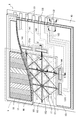
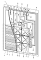
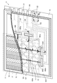
- FIG. 2 is a partial cutaway view showing a schematic configuration of the touch panel according to the first embodiment of the present invention.
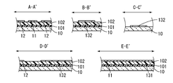
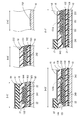
- FIG. 3 is a cross-sectional view taken along lines A-A ′, B-B ′, C-C ′, D-D ′, and E-E ′ in FIG. 2.
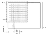
- FIG. 4A is a plan view showing only the substrate, the black matrix, and the planarizing film extracted from the configuration of the touch panel according to the first embodiment of the present invention.
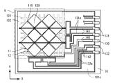
- FIG. 4B is a plan view showing the configuration of FIG. 4A with an X electrode, a Y electrode, and a terminal added.
- FIG. 4C is a plan view showing a part of the wiring added to the configuration of FIG. 4B.
- 4D is a plan view showing the structure of FIG. 4C with an insulating film added.
- FIG. 4E is a plan view showing a part of the wiring added to the configuration of FIG. 4D.
- FIG. 4F is a plan view showing the structure of FIG. 4E with a protective film and a color filter added thereto.
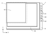
- FIG. 4G is a plan view in which a common electrode is further added to the configuration of FIG. 4F and is a plan view of the touch panel according to the first embodiment of the present invention.
- FIG. 5A is a cross-sectional view for explaining the method for manufacturing the touch panel according to the first embodiment of the present invention.
- FIG. 5A is a cross-sectional view for explaining the method for manufacturing the touch panel according to the first embodiment of the present invention.
- FIG. 5B is a cross-sectional view for explaining the touch panel manufacturing method according to the first embodiment of the present invention.
- FIG. 5C is a cross-sectional view for explaining the touch panel manufacturing method according to the first embodiment of the present invention.
- FIG. 5D is a cross-sectional view for explaining the method for manufacturing the touch panel according to the first embodiment of the present invention.
- FIG. 5E is a cross-sectional view for explaining the touch panel manufacturing method according to the first embodiment of the present invention.
- FIG. 5F is a cross-sectional view for explaining the method for manufacturing the touch panel according to the first embodiment of the present invention.
- FIG. 5G is a cross-sectional view for explaining the method for manufacturing the touch panel according to the first embodiment of the present invention.
- FIG. 6 is a partial cutaway view showing a schematic configuration of the touch panel according to the second embodiment of the present invention.
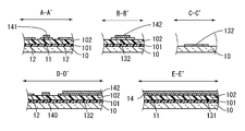
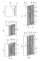
- FIG. 7 is a cross-sectional view taken along lines A-A ′, B-B ′, C-C ′, D-D ′, and E-E ′ in FIG. 6.
- FIG. 8 is a partial cutaway view showing a schematic configuration of the touch panel according to the third embodiment of the present invention.
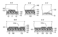
- FIG. 9 is a cross-sectional view taken along lines A-A ′, B-B ′, C-C ′, D-D ′, and E-E ′ in FIG. 8.
- FIG. 10 is a partial cutaway view showing a schematic configuration of a touch panel according to the fourth embodiment of the present invention.
- FIG. 10 is a partial cutaway view showing a schematic configuration of a touch panel according to the fourth embodiment of the present invention.
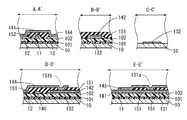
- FIG. 11 is a cross-sectional view taken along lines A-A ′, B-B ′, C-C ′, D-D ′, and E-E ′ in FIG. 10.
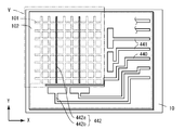
- FIG. 12A is a plan view showing a substrate, a black matrix, a planarizing film, and a part of wiring extracted from the configuration of the touch panel according to the fourth embodiment of the present invention.
- 12B is a plan view showing the structure of FIG. 12A with an additional insulating film.
- FIG. 12C is a plan view showing the configuration of FIG. 12B with an X electrode, a Y electrode, and a terminal added.
- 12D is a plan view showing a part of the wiring added to the configuration of FIG. 12C.
- FIG. 12A is a plan view showing a substrate, a black matrix, a planarizing film, and a part of wiring extracted from the configuration of the touch panel according to the fourth embodiment of the present invention.
- 12B is a plan view showing the structure of FIG
- FIG. 13 is a partial cutaway view showing a schematic configuration of a touch panel according to a fifth embodiment of the present invention.
- FIG. 14 is a cross-sectional view taken along lines A-A ′, B-B ′, C-C ′, D-D ′, and E-E ′ in FIG. 13.
- FIG. 15A is a plan view illustrating a substrate, a black matrix, a planarization film, an X electrode, a Y electrode, a terminal, and some wirings extracted from the configuration of the touch panel according to the fifth embodiment of the present invention.
- FIG. 15B is a plan view showing a part of the wiring extracted from the configuration of the touch panel according to Embodiment 5 of the present invention.
- FIG. 16 is a partial cutaway view showing a schematic configuration of a touch panel according to a sixth embodiment of the present invention.
- FIG. 17 is a cross-sectional view taken along the lines A-A ′, B-B ′, C-C ′, D-D ′, and E-E ′ in FIG. 16.
- FIG. 18 is sectional drawing which shows schematic structure of the display apparatus with a touchscreen concerning other embodiment of this invention.
- FIG. 19 is a partial cutaway view showing a schematic configuration of a touch panel according to a seventh embodiment of the present invention.
- 20 is a cross-sectional view taken along lines A-A ′, B-B ′, C-C ′, D-D ′, and E-E ′ in FIG. 19.
- a touch panel includes an insulating substrate, a first light shielding portion formed along a first direction, and a second formed along a second direction intersecting the first direction.
- a plurality of first island electrodes arranged along the first direction; a plurality of second island electrodes arranged along the second direction; and the plurality of first island electrodes.
- the first metal film overlaps the first light shielding part in a plan view, the width of the first metal film is narrower than the width of the first light shielding part, and the second metal film is the second light shielding part. And the width of the second metal film is narrower than the width of the second light shielding portion, and the first and second island electrodes are formed of a transparent conductive film (first configuration). ).
- the first and second metal films are formed in contact with the plurality of first and second island electrodes, respectively.
- the electrical resistance of a 1st and 2nd island-like electrode can be made low, and a sensitivity can be made high.
- the first and second metal films are formed so as to overlap with the first and second light shielding portions, respectively, in plan view. Further, the widths of the first and second metal films are formed narrower than the widths of the first and second light shielding parts, respectively. Thereby, a metal film with high reflectance is not visually recognized by an observer. In addition, the aperture ratio of the display device is not reduced.
- the first and second light shielding portions are formed on the substrate, and further include a planarization film formed to cover the first and second light shielding portions and the substrate; (Second configuration).
- the plurality of first island electrodes are preferably connected to each other in the first direction (third configuration).
- the first island-shaped electrodes are connected to each other in addition to the first island-shaped electrodes being connected by the first metal film.
- the first metal film is formed above the first island-like electrode and below the insulating film, and the second metal film is formed from the first island-shaped electrode. It can be set as the structure formed in the upper layer from the two island-like electrode and the said insulating film (4th structure).
- the first metal film is formed below the first island electrode and the insulating film
- the second metal film includes the second island electrode and It can be set as the structure formed in the upper layer from the said insulating film (5th structure).
- the first metal film is formed above the first island-shaped electrode and the insulating film, and the second metal film includes the second island-shaped electrode and the second island-shaped electrode. It can be set as the structure formed in the lower layer from the said insulating film (6th structure).
- the first light-shielding portion is in contact with at least one of the first island-shaped electrode and the first metal film and overlaps the first light-shielding portion in plan view. It is preferable to further include a third metal film formed with a narrower width than the portion (seventh configuration).
- the second light-shielding portion is in contact with at least one of the second island-shaped electrode and the second metal film and overlaps the second light-shielding portion in plan view. It is preferable to further include a fourth metal film formed with a narrower width than the portion (eighth configuration).
- the reliability can be improved and the yield can be improved.
- the insulating film is formed to cover the first and second island-shaped electrodes, the first island-shaped electrode, the first metal film, and the first It can be set as the structure which has an opening part for connecting at least one of a 2 island-like electrode and the said 2nd metal film (9th structure).
- any one of the first to ninth configurations it is preferable to further include a wiring formed of the same material as at least one of the first and second metal films (tenth configuration).
- one of the first and second metal films and the wiring can be manufactured in the same process. Therefore, the manufacturing process can be simplified.
- the redundant structure of the wiring and the transparent conductive film can increase the reliability and improve the yield.
- the redundant structure of the wiring and the fifth metal film can improve the reliability and improve the yield.
- Any one of the first to twelfth configurations may further include a color filter layer (a thirteenth configuration).
- the insulating film has a width in the first direction smaller than a width of the second light shielding portion, or a width in the second direction smaller than a width of the first light shielding portion. Preferably (fourteenth configuration).
- the thickness of the color filter layer changes and the color changes.
- all of these are formed at a location overlapping with the first or second light-shielding portion, so that the change in color of the color filter layer is not visually recognized by the observer. Therefore, it is not necessary to separately form a flattening film, and the manufacturing process can be simplified.
- a display device with a touch panel includes a touch panel having any one of the first to fourteenth configurations, a common electrode formed on the touch panel, and a thin film transistor substrate disposed to face the touch panel. And a liquid crystal sandwiched between the touch panel and the thin film transistor substrate (first configuration of a display device with a touch panel).
- the thin film transistor substrate preferably includes an oxide semiconductor layer containing indium gallium zinc oxide (second configuration of the display device with a touch panel).
- Indium gallium zinc oxide has high electron mobility and small variations in characteristics. By using indium gallium zinc oxide, a display device with a touch panel can be increased in size and definition.
- FIG. 1 is a cross-sectional view showing a schematic configuration of a display device 8 with a touch panel according to an embodiment of the present invention.
- the display device 8 with a touch panel includes a touch panel 1, a thin film transistor (TFT) substrate 81, polarizing plates 82 and 83, a sealing material 84, and a liquid crystal 85.
- TFT thin film transistor
- the touch panel 1 and the TFT substrate 81 are arranged to face each other.
- a sealing material 84 is formed on the peripheral portions of the touch panel 1 and the TFT substrate 81, and a liquid crystal 85 is sealed inside.
- Polarizers 82 and 83 are disposed on the outer surfaces of the touch panel 1 and the TFT substrate 81, respectively.
- the touch panel 1 is a capacitive touch panel, which will be described in detail later, and includes an insulating substrate 10 and sensor electrode groups (X electrode 11, Y electrode 12, etc.).
- the X electrode 11 and the Y electrode 12 are formed in a lattice shape.
- the X electrode 11 and the Y electrode 12 form a capacitance between a finger and the like that are close to each other with the substrate 10 in between.
- the touch panel 1 detects the position of a finger or the like based on the change in capacitance.
- the touch panel 1 further includes a black matrix 101, a color filter 17, a common electrode 18, and the like.
- the TFT substrate 81 includes an insulating substrate 811, a pixel electrode 812, and a TFT (not shown).
- the pixel electrodes 812 and the TFTs are arranged in a matrix on the substrate 811.
- a TFT having an amorphous silicon layer, an oxide semiconductor layer, or the like can be used as a TFT, but an oxide semiconductor layer, particularly an oxide semiconductor layer containing indium gallium zinc oxide (IGZO or IZGO) is preferably used.
- IGZO has a high electron mobility and a small variation in characteristics. Therefore, it is advantageous for enlargement and high definition of the display device 8 with a touch panel.
- the display device 8 with a touch panel drives the TFT of the TFT substrate 81 to generate an electric field between the arbitrary pixel electrode 812 and the common electrode 18. This electric field changes the orientation of the liquid crystal 85.
- Light incident from the polarizing plate 83 side is polarized in a specific direction by the polarizing plate 83.
- the polarization direction of the light incident on the liquid crystal 85 changes depending on the orientation of the liquid crystal 85. Only light polarized in a specific direction is transmitted through the polarizing plate 82.
- the display device with a touch panel 8 can control light transmission / non-transmission at an arbitrary pixel electrode 812.
- the light transmitted through the pixel electrode 812 is colored by the color filter 17.
- the color filters 17 of a plurality of colors for example, red, green, and blue regularly, various colors can be displayed by additive color mixture.
- the black matrix 101 shields light from a part other than the part where the pixel electrode 812 is formed, and improves the contrast.
- the display device with a touch panel 8 is an in-cell type display device with a touch panel in which a sensor electrode group of the touch panel is formed on a so-called color filter substrate of the liquid crystal display device.
- FIG. 2 is a partial cutaway view schematically showing a schematic configuration of the touch panel 1 according to the first embodiment of the present invention.
- 3 is a cross-sectional view taken along lines AA ′, BB ′, CC ′, DD ′, and EE ′ in FIG.
- the touch panel 1 includes a substrate 10, a black matrix 101, a planarizing film 102, an X electrode 11, a Y electrode 12, terminals 130 to 132, wirings 140 to 144, insulating films 151 and 152, a protective film 16, a color filter 17, and a common An electrode 18 is provided.
- the touch panel 1 has a display area V and other frame areas as shown in FIG.
- the X electrode 11 and the Y electrode 12 that are sensor electrodes are formed in the display region V.
- the X electrode 11 and the Y electrode 12 are electrically connected to terminals 131 and 132 formed in the vicinity of the end portion of the substrate 10 through wirings 141 to 144 and the like. Note that the terminal 130 and the wiring 140 are not connected to either the X electrode 11 or the Y electrode 12. These function as shield wires that shield electromagnetic noise. Terminals 130 to 132 are connected to a drive circuit via an FPC (Flexible Printed Circuit) not shown.
- FPC Flexible Printed Circuit
- FIG. 4A is a plan view showing only the substrate 10, the black matrix 101, and the planarization film 102 extracted from the configuration of the touch panel 1.
- FIG. 4A the black matrix 101 and the planarization film 102 are formed on the substrate 10.
- the horizontal direction in FIG. 4A is referred to as the X direction
- the vertical direction in FIG. 4A is referred to as the Y direction.
- the black matrix 101 includes a first light shielding part 101a, a second light shielding part 101b, and a third light shielding part 101c.
- first light shielding portions 101a formed along the X direction and a plurality of second light shielding portions 101b formed along the Y direction are formed in a lattice shape.
- the first light-shielding part 101 a and the second light-shielding part 101 b are formed so that each rectangular area surrounded by them corresponds to a unit pixel of the display device 8.
- a uniform light shielding portion 101c is formed.
- a flattening film 102 is formed so as to cover the entire black matrix 101 and a part of the substrate 10.
- FIG. 4B is a plan view showing the configuration shown in FIG. 4A with the X electrode 11, the Y electrode 12, and the terminals 130 to 132 added thereto. As shown in FIG. 4B, the X electrode 11 and the Y electrode 12 are formed on the planarizing film 102. The terminals 130 to 132 are formed across the planarizing film 102 and the substrate 10.
- the X electrode 11 is composed of a plurality of island electrodes 110 arranged along the X direction.
- the Y electrode 12 includes a plurality of island electrodes 120 arranged along the Y direction.
- the plurality of island electrodes 110 are connected to each other in the X direction.
- the island electrodes 120 are arranged discretely.
- the terminals 131 and 132 are elongated from the vicinity of the end portion of the substrate 10 to the vicinity of the X electrode 11 and the Y electrode 12.
- the terminal 131 and the X electrode 11 are connected, but the terminal 132 and the Y electrode 12 are not connected.
- portions of the terminals 131 and 132 that overlap with the third light-shielding portion 101c in plan view are referred to as extension portions 131a and 132a, respectively.
- FIG. 4C is a plan view showing the configuration shown in FIG. 4B with wirings 140 to 142 added thereto.
- the wiring 141 is formed on the X electrode 11 and the extending portion 131 a of the terminal 131.
- the wiring 142 is formed on the extending portion 132 a of the terminal 132.
- the wiring 140 is formed on the terminal 130 and the planarization film 102.
- the wiring 141 is formed so as to overlap with the extending part 131a.
- the wiring 141 is further formed in the display region V in contact with the plurality of island electrodes 110 of the X electrode 11 along the X direction.
- the wiring 141 is formed so as to overlap with the first light shielding portion 101a in a plan view, and is formed to have a narrower width than the first light shielding portion 101a.
- the wiring 142 is formed so as to overlap the extended portion 132a. Unlike the wiring 141, the wiring 142 is not connected to the Y electrode 12 or the like.
- FIG. 4D is a plan view showing the structure of FIG. 4C with insulating films 151 and 152 added thereto.
- the insulating film 151 is formed on the planarizing film 102, the terminals 130 to 132, and the wirings 140 to 142.
- the insulating film 152 is formed on the planarizing film 102, the X electrode 11, and the wiring 141.
- the insulating film 151 is formed in a portion overlapping the third light shielding portion 101c in plan view.
- the insulating film 151 completely covers the wirings 140 and 142, and also covers a part of the terminals 130 to 132 and the wiring 141.
- the insulating film 151 is formed to protect the wirings 140 to 142 from chemicals used in the manufacturing process or the like.
- a contact hole 151a for connecting to the wiring 141 and a contact hole 151b for connecting to the wiring 142 are formed.
- the insulating film 152 is formed in a portion where a wiring 141 and a wiring 143 (not shown in FIG. 4D) described later intersect.
- the insulating film 152 is formed so as to cover a part of the wiring 141 and a part of the X electrode 11.
- FIG. 4E is a plan view showing the configuration of FIG. 4D with wirings 143 and 144 added. As shown in FIG. 4E, the wiring 143 is formed on the insulating film 151 and the wiring 141. The wiring 144 is formed on the insulating films 151 and 152 and the Y electrode 12.
- the wiring 143 is in contact with the wiring 141 through a contact hole 151a formed in the insulating film 151 (see a cross-sectional view along the line E-E 'in FIG. 3).
- the wiring 141 is partially overlapped.
- the wiring 143 is formed so as to overlap with the first light shielding part 101a in a plan view, and is formed with a width narrower than that of the first light shielding part 101a.
- the wiring 144 is in contact with the wiring 142 through a contact hole 151b formed in the insulating film 151 (see a cross-sectional view along the line D-D 'in FIG. 3).
- the wiring 144 is further formed in the display region V so as to be in contact with the plurality of island-shaped electrodes 120 of the Y electrode 12 via the insulating film 152.
- the wiring 144 is formed so as to overlap with the second light-shielding part 101b in a plan view, and is formed with a width narrower than that of the second light-shielding part 101b.
- FIG. 4F is a diagram in which a protective film 16 and a color filter 17 are further added to the configuration of FIG. 4E.
- the protective film 16 is formed on the planarizing film 102, the X electrode 11, the Y electrode 12, the terminals 130 to 132, and the wirings 140 to 144.
- the X electrode 11, the Y electrode 12, and the wirings 140 to 144 are completely covered with the protective film 16.
- the terminals 130 to 132 are partly covered with the protective film 16 and partly exposed without being covered with the protective film 16.
- the color filter 17 is formed with a certain thickness on the surface flattened by the protective film 16.
- the color filter 17 is formed in the display area V.
- the color filter 17 includes a plurality of regularly arranged red colorants 171, green colorants 172, and blue colorants 173.
- the respective boundaries between the red colorant 171, the green colorant 172, the green colorant 172, the blue colorant 173, the blue colorant 173, and the red colorant 171 are in the second light-shielding part 101 b of the black matrix 101 in plan view. It is formed to overlap.
- the configuration of the color filter 17 is arbitrary, and other color combinations or four or more colorants may be provided. Further, in the present embodiment, the configuration in which the red colorant 171, the green colorant 172, and the blue colorant 173 are arranged in a stripe shape is illustrated, but the arrangement method is also arbitrary.
- FIG. 4G is a plan view in which the common electrode 18 is further added to the configuration in FIG. 4F, and is a plan view of the touch panel 1.
- FIG. 4G the common electrode 18 is formed almost entirely on the protective film 16 and the color filter 17.
- FIGS. 4A to 4G and FIGS. 5A to 5G are cross-sectional views taken along the lines AA ′, BB ′, CC ′, DD ′, and EE ′ in FIG. .
- a black matrix 101 and a planarizing film 102 are formed on a substrate 10.
- the substrate 10 is, for example, a glass substrate.
- a low reflection metal such as chromium or a black resin can be used.
- a black resin it is preferable to use a black resin.
- a sensor electrode group (X electrode 11, Y electrode 12, etc.) is formed on the upper layer of the black matrix 101. If black resin is used as the black matrix 101, the capacitance formed in the sensor electrode group is not affected.
- the black resin is obtained by dispersing a black pigment in a photoresist containing, for example, an acrylic resin or a novolac resin.
- the photoresist may be either a positive type in which the solubility in the developer decreases when exposed to light or a negative type in which the solubility in the developer increases when exposed to light.
- a black resin is uniformly applied to the entire surface of the substrate 10 by a spin coater or a slit coater.
- the thickness of the black resin to be applied is not particularly limited, but is, for example, 0.1 to 2.0 ⁇ m. After applying the black resin, patterning by photolithography is performed to form the black matrix 101.
- a planarizing film 102 is formed so as to cover the entire black matrix 101 and a part of the substrate 10.
- the planarizing film 102 is, for example, an acrylic resin.
- the planarizing film 102 can be formed by a spin coater or a slit coater. At this time, the planarization film 102 is not formed on the end portion of the substrate 10 using a metal mask or the like.
- the thickness of the planarization film 102 may be equal to or greater than the thickness of the black matrix 101.
- the X electrode 11, the Y electrode 12, and the terminals 130 to 132 are formed on the substrate 10 and the planarizing film.
- a uniform transparent conductive film is formed on the substrate 10 and the planarizing film 102 by sputtering or CVD (Chemical Vapor Deposition).
- the transparent conductive film is, for example, ITO or IZO.
- the thickness of the transparent conductive film is not particularly limited, but is 10 to 50 nm, for example.
- the transparent conductive film formed on the substrate 10 and the planarizing film 102 is patterned by photolithography. Specifically, a mask made of a photoresist is formed at a place where the X electrode 11, the Y electrode 12, and the terminals 130 to 132 are formed. Then, the remaining part is removed by etching.
- the etching method is arbitrary, for example, oxalic acid or a mixed acid of phosphoric acid / acetic acid / nitric acid can be used.
- annealing is performed in a temperature range of 200 to 250 ° C.
- the amorphous transparent conductive film (X electrode 11, Y electrode 12, terminals 130 to 132) is polycrystallized.
- a metal film is formed on the entire surface, covering the substrate 10, the planarizing film 102, the X electrode 11, the Y electrode 12, and the terminals 130 to 132 by sputtering or vapor deposition.
- the metal film is a film of a low resistance metal such as Al.
- the metal film preferably has a structure in which a plurality of metals are laminated in order to improve adhesion to a lower layer or an upper layer and corrosion resistance.
- a film in which MoNb, Al, and MoNb are stacked in this order can be used.
- the thickness of the metal film is not particularly limited, but is 0.3 to 1.0 ⁇ m, for example.
- the metal film formed on the entire surface of the substrate 10 is patterned by photolithography. Specifically, a mask made of a photoresist is formed at a place where the wirings 140 to 142 are to be formed. Then, the remaining part is removed by etching. Although the etching method is arbitrary, for example, a mixed acid of phosphoric acid / acetic acid / nitric acid or the like can be used.
- insulating films 151 and 152 are formed.
- the insulating films 151 and 152 either an organic insulator or an inorganic insulator may be used.
- the organic insulator is, for example, a photoresist containing acrylic resin, novolac resin, or the like.
- a photoresist is uniformly applied to the entire surface of the substrate 10 by a spin coater or a slit coater.
- the insulating film 151 is for protecting the wirings 140 to 142 as described above, and is preferably thicker.
- the thickness of the photoresist is not particularly limited, but is, for example, 1.5 to 3.0 ⁇ m.
- the photoresist formed on the entire surface of the substrate 10 is patterned by photolithography to form insulating films 151 and 152. At this time, contact holes 151a and 151b are also formed.
- the inorganic insulator is, for example, SiN, SiO 2 , SiON or the like.
- a uniform inorganic film made of these materials is formed on the entire surface of the substrate 10 by CVD.
- the thickness of the inorganic film is preferably thick, and is preferably twice or more the thickness of the wirings 140 to 142.
- the inorganic film formed on the entire surface of the substrate 10 is patterned by photolithography. Specifically, a mask made of a photoresist is formed where the insulating films 151 and 152 are to be formed. Then, the remaining part is removed by etching. At this time, contact holes 151a and 151b are also formed.
- the etching method is arbitrary, for example, dry etching using a fluorine-based gas can be used.
- wirings 143 and 144 are formed.
- a metal film is formed on the entire surface by sputtering or vapor deposition so as to cover the substrate 10, the planarizing film 102, the X electrode 11, the Y electrode 12, the terminals 130 to 132, the wiring 141, and the insulating films 151 and 152.
- the same material as that used for forming the wirings 140 to 142 may be used, or a different material may be used.
- As the metal film for example, a film in which MoNb, Al, and MoNb are stacked in this order can be used.
- the thickness of the metal film is not particularly limited, but is 0.3 to 1.0 ⁇ m, for example.
- the metal film formed on the entire surface of the substrate 10 is patterned by photolithography. Specifically, a mask made of a photoresist is formed at a place where the wirings 143 and 144 are formed. Then, the remaining part is removed by etching.
- the etching method is arbitrary, for example, a mixed acid of phosphoric acid / acetic acid / nitric acid or the like can be used. At this time, the etching time is adjusted so that the wiring 141 is not etched.
- a protective film 16 and a color filter 17 are formed.
- the protective film 16 is formed so as to cover almost the entire surface of the substrate 10.
- the protective film 16 is, for example, an acrylic resin.
- the protective film 16 may be formed by forming an inorganic film such as SiN, SiO 2 or SiON and further forming a film such as an acrylic resin thereon.
- the inorganic film can be formed by, for example, CVD.
- a film such as an acrylic resin can be formed by, for example, a spin coater or a slit coater. At this time, a part of the terminals 130 to 132 is exposed using a metal mask or the like so that the protective film 16 is not formed on the end portion of the substrate 10.
- the thickness of the protective film 16 is not particularly limited, but is, for example, 1.5 to 3.0 ⁇ m.
- a color filter 17 is formed on the protective film 16.
- a coloring material in which a pigment or dye is dispersed or dissolved in a resin or the like can be used.
- the color filter 17 is formed by repeatedly performing patterning by photolithography, for example. Specifically, first, a red colorant is uniformly applied on the protective film 16 by a slit coater or a spin coater. Thereafter, patterning is performed to form a red coloring material 171.
- the green colorant 172 and the blue colorant 173 are formed by repeating this process.
- the color filter 17 can also be formed by an inkjet method. Specifically, first, a mixed composition of a red colorant and a solvent is applied to a predetermined location on the protective film 16 by inkjet. Thereafter, the solvent is dried, cured, fired, and the like to form the red coloring material 171. Hereinafter, the green colorant 172 and the blue colorant 173 are formed by repeating this process.
- the common electrode 18 is a transparent conductive film such as ITO or IZO, for example.
- a uniform common electrode 18 is formed on substantially the entire surface of the substrate 10 by sputtering or CVD, covering the protective film 16 and the color filter 17. At this time, by using a metal mask or the like, the common electrode 18 is not formed at the end portion of the substrate 10 and is not in contact with the terminals 130 to 132 and the like.
- the thickness of the common electrode 18 is not particularly limited, but is 10 to 50 nm, for example.
- the wiring 141 is formed in contact with the plurality of island electrodes 110 of the X electrode 11. Further, the wiring 144 is formed in contact with the plurality of island electrodes 120 of the Y electrode 12. Thereby, the electroconductivity of X electrode 11 and Y electrode 12 can be improved, and a sensitivity can be improved.
- the wiring 141 overlaps with the first light shielding portion 101a of the black matrix 101 in a plan view and is formed to be narrower than the width of the first light shielding portion 101a.
- the wiring 144 overlaps with the second light shielding part 101b of the black matrix 101 in plan view, and is formed to be narrower than the width of the second light shielding part 101b.
- the plurality of island-like electrodes 110 and the terminals 131 constituting the X electrode 11 are continuously and integrally formed. That is, the X electrode 11 and the terminal 131 are electrically connected by themselves. In addition to this, the plurality of island electrodes 110 and the terminals 131 are further electrically connected by wiring 141. Further, the wiring 143 is formed so as to partially overlap the wiring 141. With such a redundant structure, resistance can be reduced, wiring reliability can be improved, and yield can be improved.
- the wirings 141 and 142 and the extending portions 131a and 132a of the terminals 131 and 132 are formed so as to overlap each other.
- resistance can be reduced, wiring reliability can be improved, and yield can be improved.
- the X electrode 11, the Y electrode 12, and the terminals 130 to 132 are formed using the same material and the same process. Further, the wiring 141 is formed in the same material and in the same process together with the wirings 140 and 142 in the display region V and the frame region other than the display region V. Thus, according to this embodiment, the number of times of patterning can be reduced and the manufacturing process can be simplified.
- the display device with a touch panel 8 may include any of touch panels 2 to 6 described below instead of the touch panel 1.
- FIG. 6 is a partial cutaway view schematically showing a schematic configuration of the touch panel 2 according to the second embodiment of the present invention.
- FIG. 7 is a cross-sectional view taken along lines A-A ′, B-B ′, C-C ′, D-D ′, and E-E ′ in FIG. 6.
- the touch panel 2 includes a substrate 10, a black matrix 101, a planarizing film 102, an X electrode 21, a Y electrode 22, terminals 230 to 232, wirings 143, 144, and 240 to 242, insulating films 151 and 152, a protective film 16, and a color filter. 17 and a common electrode 18.
- the touch panel 2 is different from the touch panel 1 in the configuration of X electrodes, Y electrodes, terminals, and wiring.
- the wirings 240 to 242 are formed in layers below the X electrode 21, the Y electrode 22, and the terminals 230 to 232.
- the touch panel 1 first, the X electrode 11, the Y electrode 12, and the terminals 130 to 132 were formed on the planarization film 102 (see FIG. 4B). Then, wirings 140 to 142 were formed thereon (see FIG. 4C). On the other hand, in the touch panel 2, the wirings 240 to 242 are formed first, and then the X electrode 21, the Y electrode 22, and the terminals 230 to 232 are formed.
- FIG. 8 is a partial cutaway view schematically showing a schematic configuration of the touch panel 3 according to the third embodiment of the present invention.
- FIG. 9 is a cross-sectional view taken along lines AA ′, BB ′, CC ′, DD ′, and EE ′ in FIG.
- the touch panel 3 includes a substrate 10, a black matrix 101, a planarizing film 102, an X electrode 11, a Y electrode 12, terminals 130 to 132, wirings 140 to 144, insulating films 151 and 352, a color filter 37, and a common electrode 38. ing.
- the touch panel 3 is different from the touch panel 1 in the configuration of the insulating film, the color filter, and the common electrode. Further, the touch panel 3 does not have a configuration corresponding to the protective film 16 included in the touch panel 1.
- a color filter 37 is formed on almost the entire surface of the substrate 10 instead of the protective film 16 included in the touch panel 1.
- a common electrode 38 is formed on the color filter 37. That is, in the touch panel 3, the color filter 37 also serves as a protective film.
- the thickness of the color filter 37 is not uniform due to the thickness of the insulating film 352 and the wirings 141 and 144 formed immediately below the color filter 37. Specifically, the thickness of the color filter 37 is thin at the portion where the layer immediately below is thick. A portion where the thickness of the color filter 37 is thin has low saturation. That is, if the thickness of the color filter 37 is non-uniform, the displayed color becomes non-uniform.
- the insulating film 352 is formed so as to overlap the second light shielding part 101 b of the black matrix 101 in a plan view and to be narrower than the width of the second light shielding part 101 b.
- the wiring 141 overlaps with the first light shielding part 101a of the black matrix 101 in a plan view and is formed to be narrower than the width of the first light shielding part 101a.
- the wiring 144 overlaps with the second light shielding part 101b of the black matrix 101 in plan view, and is formed to be narrower than the width of the second light shielding part 101b.
- the portion where the thickness of the color filter 37 is reduced by the wirings 141 and 144 and the insulating film 352 is shielded by the black matrix 101 and is not visually recognized by the observer.
- the formation of the protective film 16 on the touch panel 1 can be omitted. Thereby, the number of manufacturing steps can be reduced, and the yield can be improved.
- the configuration in which the insulating film 352 is shielded by the second light shielding portion 101b of the black matrix 101 is shown.
- the insulating film 352 may be configured to be shielded by the first light shielding portion 101a.
- the insulating film 352 may be formed so as to overlap with the first light shielding portion 101a in plan view and to be narrower than the width of the first light shielding portion 101a.
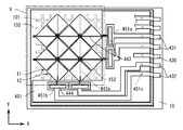
- FIG. 10 is a partial cutaway view schematically showing a schematic configuration of the touch panel 4 according to the fourth embodiment of the present invention.
- FIG. 11 is a cross-sectional view taken along lines AA ′, BB ′, CC ′, DD ′, and EE ′ in FIG.
- the touch panel 4 includes a substrate 10, a black matrix 101, a planarizing film 102, an X electrode 41, a Y electrode 42, terminals 430 to 432, wirings 440 to 444, insulation 152 and 451, a protective film 16, a color filter 17, and a common electrode. 18 is provided.
- the touch panel 4 is different from the touch panel 1 in the configuration of the X electrode, the Y electrode, the terminal, the wiring, and the insulating film.
- the X electrode 11, the Y electrode 12, and the terminals 130 to 132 were formed on the planarizing film 102 (see FIG. 4B), and the wirings 140 to 142 were formed thereon (see FIG. 4C). Then, insulating films 151 and 152 were formed thereon (see FIG. 4D), and wirings 143 and 144 were further formed thereon (see FIG. 4E). On the other hand, in the touch panel 4, the X electrode, the Y electrode, and the terminal are formed after the insulating film is formed.
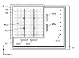
- wirings 440 to 442 are formed on the planarizing film 102. Similar to the wiring 140 of the touch panel 1, the wiring 440 is a shield wire for shielding electromagnetic noise. Unlike the wiring 141 of the touch panel 1, the wiring 441 is not formed in the display region V. On the other hand, the wiring 442 is formed in the display region V so as to overlap with the second light shielding part 101b of the black matrix 101 and to be narrower than the width of the second light shielding part 101b. A wiring 442 (referred to as a wiring 442a) formed in the display area V and a wiring 442 (referred to as a wiring 442b) formed in a frame area other than the display area V are not connected.
- an insulating film 451 is formed to cover the planarization film 102 and the wirings 440 to 442.
- Contact holes 451a to 451c are formed in the insulating film 451.
- the insulating film 152 is formed so as to cover part of the wiring 442a.
- an X electrode 41, a Y electrode 42, and terminals 430 to 432 are formed.
- the X electrode 41 is composed of a plurality of island-like electrodes 410 arranged along the X direction, like the X electrode 11 of the touch panel 1.
- the Y electrode 12 is composed of a plurality of island electrodes 420 arranged along the Y direction.
- the plurality of island electrodes 410 are connected to each other in the X direction.
- the island electrodes 420 are discretely arranged.
- the island-shaped electrodes 420 in the Y direction are electrically connected to each other by the wiring 442a.
- the X electrode 41 and the wiring 442a are insulated by the insulating film 152.
- the X electrode 41 and the terminal 431 are integrally formed continuously.
- the Y electrode 42 and the terminal 432 are not connected.
- the terminal 431 and the wiring 441 are electrically connected through contact holes 451a and 451c.
- the terminal 432 and the wiring 442b are electrically connected through contact holes 451b and 451c.
- the terminal 430 and the wiring 440 are electrically connected through a contact hole 451c.
- wirings 443 and 444 are formed.
- the wiring 443 is formed so as to partially overlap the terminal 431.
- the wiring 443 is formed so as to be in contact with the plurality of island electrodes 410 of the X electrode 41.
- the wiring 443 is formed so as to overlap with the first light shielding portion 101a of the black matrix 101 in a plan view and to be narrower than the width of the first light shielding portion 101a.
- the wiring 444 is formed so as to partially overlap the terminal 432 and the Y electrode 42 and electrically connects the terminal 432 and the Y electrode 42.
- the wiring 442a is formed in contact with the plurality of island-shaped electrodes 420 of the Y electrode 42.
- a wiring 443 is formed in contact with the plurality of island electrodes 410 of the X electrode 41.
- the wirings 442 and 443 are shielded by the black matrix 101 and are not visually recognized by an observer, and the aperture ratio of the display device 8 is not reduced.
- the plurality of island-like electrodes 410 and the terminals 431 are integrally formed continuously. Further, the wirings 141 and 143 are electrically connected. With such a redundant structure, resistance can be reduced, wiring reliability can be improved, and yield can be improved.
- the terminal 431 and the wiring 441 have a redundant structure.
- the terminal 432 and the wiring 442b have a redundant structure. As a result, the resistance can be reduced, the reliability of the wiring can be increased, and the yield can be improved.
- the wirings 430, 431, 432a and 432b can be formed using the same material and the same process. Thereby, the number of times of patterning can be reduced and the manufacturing process can be simplified.
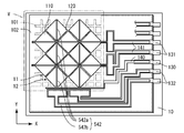
- FIG. 13 is a partial cutaway view schematically showing a schematic configuration of the touch panel 5 according to the fifth embodiment of the present invention.
- FIG. 14 is a cross-sectional view taken along lines AA ′, BB ′, CC ′, DD ′, and EE ′ in FIG.
- the touch panel 5 includes a substrate 10, a black matrix 101, a planarizing film 102, an X electrode 11, a Y electrode 12, terminals 130 to 132, wirings 140, 141, 540, 542 to 544, insulation 152 and 551, a protective film 16, a color A filter 17 and a common electrode 18 are provided.
- the touch panel 5 is different from the touch panel 1 in the configuration of wiring and insulating film.
- FIG. 15A shows the substrate 10, the black matrix 101, the planarization film 102, the X electrode 11, the Y electrode 12, the terminals 130 to 132, and the wirings 140, 141, and 542 extracted from the configuration of the touch panel 5. .
- the touch panel 5 includes a wiring 542 instead of the wiring 142 included in the touch panel 1.
- the wiring 542 is formed so as to partially overlap with the terminal 132, similarly to the wiring 142.
- the wiring 542 is further formed in the display area V so as to overlap the second light shielding part 101b of the black matrix 101 and to be narrower than the width of the second light shielding part 101b.
- the wirings 542 (referred to as the wirings 542a) formed in the display region V are discretely formed so as not to contact the wirings 141. Further, the wiring 542a is not connected to the wiring 542 (referred to as the wiring 542b) formed in the frame region other than the display region V.
- the wirings 140, 141, and 542 can be formed of the same material and in the same process as in the case of the wirings 140 to 142 in the touch panel 1. As with the touch panel 1, after the wirings 140, 141, and 542 are formed, the insulating films 152 and 551 are formed. Thereafter, wirings 540, 543, and 544 are formed.
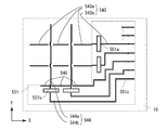
- FIG. 15B is a diagram showing wirings 540, 543, and 544 extracted from the configuration of the touch panel 5.
- the positions of the substrate 10 and the insulating film 551 are indicated by broken lines.
- the wiring 543 includes a wiring 543a formed in the display area V and a wiring 543b formed in a frame area other than the display area V.
- the wirings 543a and 543b are integrally formed continuously.
- the wiring 543a overlaps with the first light shielding part 101a of the black matrix 101 in a plan view and is formed to be narrower than the width of the first light shielding part 101a.
- the wiring 543a is discretely formed so as not to contact the wiring 544.
- the wiring 543b is formed so as to overlap with the wiring 141 in a plan view.
- the wirings 543b and 141 are electrically connected through contact holes 551a and 551c formed in the insulating film 551.
- the wiring 544 includes a wiring 544a formed in the display area V and a wiring 544b formed in a frame area other than the display area V.
- the wirings 544a and 544b are integrally formed continuously.
- the wiring 544a is formed so as to overlap with the second light shielding part 101b of the black matrix 101 in a plan view and narrower than the width of the second light shielding part 101b. Although not shown in FIG. 15B, the wiring 544a is formed so as to be in contact with the wiring 542a on the Y electrode 12 via the insulating film 152.
- the wiring 544b is formed so as to overlap with the wiring 542b in plan view.
- the wirings 544b and 542b are electrically connected through contact holes 551b and 551c formed in the insulating film 551.
- the wiring 540 is formed so as to overlap with the wiring 140 in plan view.
- the wiring 540 is discretely formed so as not to contact the wiring 544.
- the wiring 540 and the wiring 140 are electrically connected through a contact hole 551c formed in the insulating film 551.
- the wirings 540, 543, and 544 can be formed in the same material and in the same process as the wirings 143 and 144 in the touch panel 1.
- the wiring 141 is formed in contact with the plurality of island electrodes 110 of the X electrode 11.
- a wiring 544 is formed in contact with the plurality of island electrodes 120 of the Y electrode 12.
- the wiring 543a is further formed so as to partially overlap the wiring 141 in plan view.
- a triple redundant structure is formed by the X electrode 11 and the wirings 141 and 543a.
- the wiring 542b is formed so as to partially overlap with the wiring 544b in plan view.
- a triple redundant structure is formed by the Y electrode 12 and the wirings 542b and 544b.
- the terminal 131, the wiring 141, and the wiring 543b that are electrically connected to each other are formed so as to overlap each other in plan view, thereby forming a triple redundant structure.
- a terminal 132 and wirings 542 and 544b that are electrically connected to each other are formed so as to overlap each other in plan view, thereby forming a triple redundant structure.
- wirings 140 and 540 connected to each other are formed so as to overlap each other in plan view, thereby forming a redundant structure.
- the resistance can be further reduced as compared with the touch panel 1, and the wiring reliability can be further improved and the yield can be improved.
- the wirings 141, 542a, 543a, and 544a are shielded by the black matrix 101, are not visually recognized by the observer, and do not lower the aperture ratio of the display device 8.
- the wirings 140, 141, and 542 can be formed using the same material and the same process.
- the wirings 540, 543, and 544 can be formed using the same material and the same process. Thereby, the number of times of patterning can be reduced and the manufacturing process can be simplified.
- FIG. 16 is a partial cutaway view schematically showing a schematic configuration of the touch panel 6 according to the sixth exemplary embodiment of the present invention.
- FIG. 17 is a cross-sectional view taken along lines AA ′, BB ′, CC ′, DD ′, and EE ′ in FIG.
- the touch panel 6 includes a substrate 10, a black matrix 101, a planarization film 102, an X electrode 11, a Y electrode 12, terminals 130 to 132, wirings 140 to 142, 643, 644, an insulating film 650, a protective film 16, a color filter 17, And a common electrode 18.
- the touch panel 6 differs from the touch panel 1 in the configuration of the wiring and the insulating film.
- the insulating film 650 is formed so as to cover almost the entire planarizing film 102, X electrode 11, Y electrode 12, terminals 130 to 132, and wirings 140 to 142. In the insulating film 650, contact holes 650a to 650e are formed.
- wirings 643 and 644 are formed on the insulating film 650.
- the wiring 643 is electrically connected to the wiring 141 through the contact holes 650a and 650c.
- the wiring 644 is in contact with the wiring 142 and the Y electrode 12 through the contact hole 650b and the contact hole 650d. Thereby, the Y electrode 12 and the wirings 142 and 644 are electrically connected to each other.
- the wiring 644 is further in contact with the plurality of island electrodes 120 of the Y electrode 12 through the contact hole 650e. Thereby, the plurality of island electrodes 120 and the wiring 644 are electrically connected to each other.
- the wiring 664 overlaps with the second light shielding part 101b of the black matrix 101 and is formed to be narrower than the width of the second light shielding part 101b.
- FIG. 18 is a cross-sectional view showing a schematic configuration of a display device 9 with a touch panel according to another embodiment of the present invention.
- the display device 9 with a touch panel includes a touch panel 7, a TFT substrate 91, polarizing plates 82 and 83, a sealing material 84, and a liquid crystal 85.
- FIG. 19 is a partial cutaway view showing a schematic configuration of the touch panel 7 according to the seventh embodiment of the present invention.
- FIG. 20 is a cross-sectional view taken along the lines A-A ′, B-B ′, C-C ′, D-D ′, and E-E ′ in FIG. 19.
- the touch panel 7 includes a substrate 10, a black matrix 101, a planarizing film 102, an X electrode 11, a Y electrode 12, terminals 130 to 132, wirings 140 to 144, insulating films 151 and 152, a protective film 16, and a common electrode 78. ing.
- the touch panel 7 is different from the touch panel 1 in that it does not have a configuration corresponding to the color filter 17.
- the common electrode 78 is formed on the protective film 16.
- the TFT substrate 91 includes a substrate 811, a pixel electrode 812, and a color filter 913.
- the display device 9 with a touch panel has a configuration in which a color filter is formed on the TFT substrate side.
- the manufacturing process on the touch panel side can be simplified. Thereby, the yield of the touch panel 7 can be improved.
- the present invention can be industrially used as a capacitive touch panel and a display device with a touch panel.
Landscapes
- Engineering & Computer Science (AREA)
- Physics & Mathematics (AREA)
- General Engineering & Computer Science (AREA)
- Theoretical Computer Science (AREA)
- General Physics & Mathematics (AREA)
- Human Computer Interaction (AREA)
- Nonlinear Science (AREA)
- Mathematical Physics (AREA)
- Chemical & Material Sciences (AREA)
- Crystallography & Structural Chemistry (AREA)
- Optics & Photonics (AREA)
- Position Input By Displaying (AREA)
Abstract
感度の高いタッチパネルの構成を得る。タッチパネル(1)は、絶縁性の基板(10)と、第1方向に沿って形成された第1遮光部と、前記第1方向と交差する第2方向に沿って形成された第2遮光部と、前記第1方向に沿って配置された複数の第1島状電極(110)と、前記第2方向に沿って配置された複数の第2島状電極(120)と、前記複数の第1島状電極(110)に接して、前記第1方向に沿って形成された第1金属膜(141)と、前記複数の第2島状電極(120)に接して、前記第2方向に沿って形成された第2金属膜(152)と、少なくとも前記第1金属膜(151)および第2金属膜(152)が平面視において交差する箇所に形成され、前記第1金属膜(151)および第2金属膜(152)を相互に絶縁する絶縁膜(152)とを備える。
Description
本発明は、タッチパネルおよびタッチパネル付き表示装置に関し、より詳しくは、静電容量方式のタッチパネルおよびタッチパネル付き表示装置に関する。
静電容量方式のタッチパネルは、多点検出が可能である等、実用性が高く、近年普及が進んでいる。
タッチパネル付き表示装置の構成として、表示装置を構成する基板にタッチパネルの機能を持たせたインセル(in cell)型タッチパネルの構成が知られている。インセル型タッチパネルは、構成部材が少なく、薄型化・高透過率化に有利である。
特開2011-75809号公報には、液晶が2枚の無色透明な基材に挟まれ、カラー表示のためのカラーフィルタ層を一方の基材の内面側に有する構造の液晶表示パネルであって、該カラーフィルタ層を有する基材と該カラーフィルタ層との間に、静電容量式タッチパネルを有することを特徴とする液晶表示パネルが記載されている。
静電容量方式のタッチパネルは、絶縁性の基板と、格子状に形成されたセンサ電極とを備える。タッチパネルはこれらの電極と、タッチパネルに近接した指等との間に形成される静電容量の変化に基づいて、指等の位置を検出する。
これらのセンサ電極は、表示装置の表示領域と重ねて形成される。そのため通常、これらのセンサ電極は、酸化インジウムスズ(ITO:Indium Tin Oxide)、酸化インジウム亜鉛(IZO:Indium Zinc Oxide)等の透明導電膜により形成される。透明導電膜は、金属等と比較すると導電率が低い。センサ電極は、観察者から視認されにくくするために、薄く形成される必要がある。センサ電極が薄く形成されれば、センサ電極の電気抵抗は高くなる。
したがって、タッチパネルを大型化した場合、感度の低下が問題となる。
本発明の目的は、感度の高いタッチパネルの構成を得ることである。
ここに開示するタッチパネルは、絶縁性の基板と、第1方向に沿って形成された第1遮光部と、前記第1方向と交差する第2方向に沿って形成された第2遮光部と、前記第1方向に沿って配置された複数の第1島状電極と、前記第2方向に沿って配置された複数の第2島状電極と、前記複数の第1島状電極に接して、前記第1方向に沿って形成された第1金属膜と、前記複数の第2島状電極に接して、前記第2方向に沿って形成された第2金属膜と、少なくとも前記第1および第2金属膜が平面視において交差する箇所に形成され、前記第1および第2金属膜を相互に絶縁する絶縁膜とを備える。前記第1金属膜は、前記第1遮光部と平面視において重畳し、前記第1金属膜の幅は前記第1遮光部の幅よりも狭く、前記第2金属膜は、前記第2遮光部と平面視において重畳し、前記第2金属膜の幅は前記第2遮光部の幅よりも狭く、前記第1および第2島状電極は、透明導電膜で形成されている。
本発明によれば、感度の高いタッチパネルの構成が得られる。
本発明の一実施形態にかかるタッチパネルは、絶縁性の基板と、第1方向に沿って形成された第1遮光部と、前記第1方向と交差する第2方向に沿って形成された第2遮光部と、前記第1方向に沿って配置された複数の第1島状電極と、前記第2方向に沿って配置された複数の第2島状電極と、前記複数の第1島状電極に接して、前記第1方向に沿って形成された第1金属膜と、前記複数の第2島状電極に接して、前記第2方向に沿って形成された第2金属膜と、少なくとも前記第1および第2金属膜が平面視において交差する箇所に形成され、前記第1および第2金属膜を相互に絶縁する絶縁膜とを備える。前記第1金属膜は、前記第1遮光部と平面視において重畳し、前記第1金属膜の幅は前記第1遮光部の幅よりも狭く、前記第2金属膜は、前記第2遮光部と平面視において重畳し、前記第2金属膜の幅は前記第2遮光部の幅よりも狭く、前記第1および第2島状電極は、透明導電膜で形成されている(第1の構成)。
上記の構成によれば、複数の第1および第2島状電極に接して、それぞれ、第1および第2金属膜が形成されている。これにより、第1および第2島状電極の電気抵抗を低くし、感度を高くすることができる。第1および第2金属膜は、それぞれ、第1および第2遮光部と平面視において重畳するように形成されている。さらに、第1および第2金属膜の幅は、それぞれ、第1および第2遮光部の幅よりも狭く形成されている。これにより、反射率の高い金属膜が、観察者に視認されない。また、表示装置の開口率を低下させない。
上記第1の構成において、前記第1および第2遮光部は、前記基板上に形成され、前記第1および第2遮光部、ならびに前記基板を覆って形成された平坦化膜をさらに備える構成とすることができる(第2の構成)。
上記第1または第2の構成において、前記複数の第1島状電極は、前記第1方向において、相互に繋がっている構成とすることが好ましい(第3の構成)。
上記の構成によれば、複数の第1島状電極は、第1金属膜によって接続されているのに加えて、第1島状電極同士が繋がっている。このような冗長構造とすることにより、信頼性を高め、歩留まりを向上させることができる。
上記第1~第3のいずれかの構成において、前記第1金属膜は、前記第1島状電極より上層で、かつ、前記絶縁膜より下層に形成され、前記第2金属膜は、前記第2島状電極および前記絶縁膜より上層に形成されている構成とすることができる(第4の構成)。
上記第1~第3のいずれかの構成において、前記第1金属膜は、前記第1島状電極および前記絶縁膜より下層に形成され、前記第2金属膜は、前記第2島状電極および前記絶縁膜より上層に形成されている構成とすることができる(第5の構成)。
上記第1~第3のいずれかの構成において、前記第1金属膜は、前記第1島状電極および前記絶縁膜より上層に形成され、前記第2金属膜は、前記第2島状電極および前記絶縁膜より下層に形成されている構成とすることができる(第6の構成)。
上記第1~第6のいずれかの構成において、前記第1島状電極および前記第1金属膜の少なくとも一方と接して、前記第1遮光部と平面視で重畳する箇所に、前記第1遮光部より狭い幅で形成された第3金属膜をさらに備えることが好ましい(第7の構成)。
上記の構成によれば、第1金属膜と第3金属膜との冗長構造とすることにより、信頼性を高め、歩留まりを向上させることができる。
上記第1~第7のいずれかの構成において、前記第2島状電極および前記第2金属膜の少なくとも一方と接して、前記第2遮光部と平面視で重畳する箇所に、前記第2遮光部より狭い幅で形成された第4金属膜をさらに備えることが好ましい(第8の構成)。
上記の構成によれば、第2金属膜と第4金属膜との冗長構造とすることにより、信頼性を高め、歩留まりを向上させることができる。
上記第1~第8のいずれかの構成において、前記絶縁膜は、前記第1および第2島状電極を覆って形成され、前記第1島状電極と前記第1金属膜と、および前記第2島状電極と前記第2金属膜と、の少なくとも一方を接続するための開口部を有する構成とすることができる(第9の構成)。
上記第1~第9のいずれかの構成において、前記第1および第2金属膜の少なくとも一方と同一材料で形成された配線をさらに備えることが好ましい(第10の構成)。
上記の構成によれば、前記第1および第2金属膜の一方と、配線とを同一工程で作製することができる。そのため、製造工程を簡略化できる。
上記第10の構成において、前記配線と接して、前記配線と平面視において重畳する箇所に形成された透明導電膜をさらに備えることが好ましい(第11の構成)。
上記の構成によれば、配線と透明導電膜との冗長構造とすることにより、信頼性を高め、歩留まりを向上させることができる。
上記第10または第11の構成において、前記配線と電気的に接して、前記配線と異なる層に形成された第5金属膜をさらに備えることが好ましい(第12の構成)。
上記の構成によれば、配線と第5金属膜との冗長構造とすることにより、信頼性を高め、歩留まりを向上させることができる。
上記第1~第12のいずれかの構成において、カラーフィルタ層をさらに備える構成とすることができる(第13の構成)。
上記第13の構成において、前記絶縁膜は、前記第1方向の幅が前記第2遮光部の幅よりも小さい、または、前記第2方向の幅が前記第1遮光部の幅よりも小さい構成とすることが好ましい(第14の構成)。
第1および第2金属膜、ならびに絶縁膜が形成された箇所にカラーフィルタ層を形成すると、カラーフィルタ層の厚さが変化し、色味が変化してしまう。しかし、上記の構成によれば、これらはすべて、第1または第2遮光部と重畳する箇所に形成されているので、カラーフィルタ層の色味の変化は、観察者に視認されない。そのため、平坦化のための膜を別途形成する必要がなくなり、製造工程を簡略化することができる。
本発明の一実施形態にかかるタッチパネル付き表示装置は、上記第1~第14のいずれかの構成のタッチパネルと、前記タッチパネルに形成された共通電極と、前記タッチパネルに対向して配置された薄膜トランジスタ基板と、前記タッチパネルおよび前記薄膜トランジスタ基板に挟持された液晶とを備える(タッチパネル付き表示装置の第1の構成)。
上記タッチパネル付き表示装置の第1の構成において、前記薄膜トランジスタ基板は、酸化インジウムガリウム亜鉛を含む酸化物半導体層を有することが好ましい(タッチパネル付き表示装置の第2の構成)。
酸化インジウムガリウム亜鉛は、電子移動度が大きく、特性のばらつきが小さい。酸化インジウムガリウム亜鉛を用いることによって、タッチパネル付き表示装置を大型化、高精細化することができる。
[実施の形態]
以下、図面を参照し、本発明の実施の形態を詳しく説明する。図中同一または相当部分には同一符号を付してその説明は繰り返さない。なお、説明を分かりやすくするために、以下で参照する図面においては、構成が簡略化または模式化して示されたり、一部の構成部材が省略されたりしている。また、各図に示された構成部材間の寸法比は、必ずしも実際の寸法比を示すものではない。
以下、図面を参照し、本発明の実施の形態を詳しく説明する。図中同一または相当部分には同一符号を付してその説明は繰り返さない。なお、説明を分かりやすくするために、以下で参照する図面においては、構成が簡略化または模式化して示されたり、一部の構成部材が省略されたりしている。また、各図に示された構成部材間の寸法比は、必ずしも実際の寸法比を示すものではない。
[全体の構成]
図1は、本発明の一実施形態にかかるタッチパネル付き表示装置8の概略構成を示す断面図である。タッチパネル付き表示装置8は、タッチパネル1と、薄膜トランジスタ(TFT:Thin Film Transistor)基板81と、偏光板82および83と、シール材84と、液晶85とを備えている。
図1は、本発明の一実施形態にかかるタッチパネル付き表示装置8の概略構成を示す断面図である。タッチパネル付き表示装置8は、タッチパネル1と、薄膜トランジスタ(TFT:Thin Film Transistor)基板81と、偏光板82および83と、シール材84と、液晶85とを備えている。
タッチパネル1とTFT基板81とは、互いに対向して配置されている。タッチパネル1およびTFT基板81の周縁部には、シール材84が形成されており、内側に液晶85が封入されている。タッチパネル1およびTFT基板81の、外側の面には、それぞれ偏光板82および83が配置されている。
タッチパネル1は、詳しい構成は後述するが、静電容量方式のタッチパネルであり、絶縁性の基板10、センサ電極群(X電極11、Y電極12等)を備えている。X電極11およびY電極12は、格子状に形成されている。X電極11およびY電極12は、基板10を挟んで近接した指等との間に静電容量を形成する。タッチパネル1は、この静電容量の変化に基づいて、指等の位置を検出する。
タッチパネル1は、さらに、ブラックマトリクス101、カラーフィルタ17、共通電極18等を備えている。
TFT基板81は、絶縁性の基板811と、画素電極812と、図示しないTFTとを備えている。画素電極812およびTFTは、基板811にマトリクス状に配置されている。TFTとして、アモルファスシリコン層や酸化物半導体層等を有するものを用いることができるが、酸化物半導体層、特に、酸化インジウムガリウム亜鉛(IGZOまたはIZGO)を含む酸化物半導体層を用いることが好ましい。IGZOは電子移動度が大きく、特性のバラつきが小さい。そのため、タッチパネル付き表示装置8の大型化や高精細化に有利である。
タッチパネル付き表示装置8は、TFT基板81のTFTを駆動して、任意の画素電極812と共通電極18との間に電界を生成する。この電界によって、液晶85の配向が変化する。偏光板83側から入射した光は、偏光板83によって、特定の方向に偏光している。液晶85に入射した光の偏光方向は、液晶85の配向によって変化する。そして、特定の方向に偏光した光のみが、偏光板82を透過する。
このようにして、タッチパネル付き表示装置8は、任意の画素電極812において、光の透過・非透過を制御することができる。画素電極812を透過した光は、カラーフィルタ17によって着色される。複数の色、例えば赤、緑、青のカラーフィルタ17を規則的に配置しておくことにより、加法混色によって様々な色を表示することができる。ブラックマトリクス101は、画素電極812が形成されている箇所以外の箇所からの光を遮光して、コントラストを向上させる。
以上のように、本実施形態にかかるタッチパネル付き表示装置8は、液晶表示装置のいわゆるカラーフィルタ基板に、タッチパネルのセンサ電極群を作り込んだ、インセル型のタッチパネル付き表示装置である。
[タッチパネルの構成]
[第1の実施形態]
以下、タッチパネル1の構成について詳しく述べる。図2は、本発明の第1の実施形態にかかるタッチパネル1の、概略構成を模式的に示す部分破断図である。図3は、図2におけるA-A’線、B-B’線、C-C’線、D-D’線、E-E’線の各線に沿った断面図である。タッチパネル1は、基板10、ブラックマトリクス101、平坦化膜102、X電極11、Y電極12、端子130~132、配線140~144、絶縁膜151,152、保護膜16、カラーフィルタ17、および共通電極18を備えている。
[第1の実施形態]
以下、タッチパネル1の構成について詳しく述べる。図2は、本発明の第1の実施形態にかかるタッチパネル1の、概略構成を模式的に示す部分破断図である。図3は、図2におけるA-A’線、B-B’線、C-C’線、D-D’線、E-E’線の各線に沿った断面図である。タッチパネル1は、基板10、ブラックマトリクス101、平坦化膜102、X電極11、Y電極12、端子130~132、配線140~144、絶縁膜151,152、保護膜16、カラーフィルタ17、および共通電極18を備えている。
タッチパネル1は、図2に示すように、表示領域Vと、それ以外の額縁領域とを有する。センサ電極であるX電極11およびY電極12は、表示領域Vに形成されている。
X電極11およびY電極12は、配線141~144等を介して、基板10の端部付近に形成された端子131,132と電気的に接続されている。なお、端子130および配線140は、X電極11およびY電極12のいずれとも接続されていない。これらは、電磁ノイズを遮蔽するシールド線として機能する。端子130~132は、図示しないFPC(Flexible Printed Circuit)等を介して、駆動回路と接続される。
図4Aは、タッチパネル1の構成から、基板10、ブラックマトリクス101、および平坦化膜102のみを抜き出して示した平面図である。図4Aに示すように、ブラックマトリクス101および平坦化膜102は、基板10の上に形成されている。なお以下では、図4Aの左右方向をX方向、図4Aの上下方向をY方向と呼んで参照する。
ブラックマトリクス101は、第1遮光部101a、第2遮光部101b、および第3遮光部101cから構成されている。
表示領域Vにおいては、X方向に沿って形成された複数の第1遮光部101aと、Y方向に沿って形成された複数の第2遮光部101bとが、格子状に形成されている。第1遮光部101aと第2遮光部101bとは、それらによって囲まれた、それぞれの矩形領域が、表示装置8の単位画素に相当するように形成されている。
表示領域V以外の額縁領域においては、一様な遮光部101cが形成されている。
ブラックマトリクス101の全体、および基板10の一部を覆って、平坦化膜102が形成されている。
図4Bは、図4Aの構成に、さらにX電極11、Y電極12、および端子130~132を加えて示した平面図である。図4Bに示すように、X電極11およびY電極12は、平坦化膜102の上に形成されている。端子130~132は、平坦化膜102および基板10にまたがって形成されている。
X電極11は、X方向に沿って配置された複数の島状電極110から構成されている。同様に、Y電極12は、Y方向に沿って配置された複数の島状電極120から構成されている。複数の島状電極110は、X方向に互いに繋がっている。一方、島状電極120は、それぞれ離散して配置されている。
端子131および132は、基板10の端部近傍から、X電極11およびY電極12の近傍まで細長に形成されている。端子131とX電極11とは繋がっているが、端子132とY電極12とは繋がっていない。以下では、端子131および132のうち、平面視において第3遮光部101cと重畳している部分を、それぞれ延在部131aおよび132aと呼んで参照する。
図4Cは、図4Bの構成に、さらに配線140~142を加えて示した平面図である。図4Cに示すように、配線141は、X電極11および端子131の延在部131aの上に形成されている。配線142は、端子132の延在部132aの上に形成されている。配線140は、端子130および平坦化膜102の上に形成されている。
配線141は、延在部131aに重畳して形成されている。配線141はさらに、表示領域Vにおいて、X方向に沿ってX電極11の複数の島状電極110に接して形成されている。配線141は、表示領域Vにおいては、平面視において第1遮光部101aと重畳するように形成され、かつ、第1遮光部101aより狭い幅に形成されている。
配線142は、延在部132aに重畳して形成されている。配線141とは異なり、配線142は、Y電極12等へは接続されていない。
図4Dは、図4Cの構成に、さらに絶縁膜151および152を加えて示した平面図である。図4Dに示すように、絶縁膜151は、平坦化膜102、端子130~132、配線140~142の上に形成されている。絶縁膜152は、平坦化膜102、X電極11、配線141の上に形成されている。
絶縁膜151は、平面視において第3遮光部101cと重畳する部分に形成されている。絶縁膜151は、配線140,142を完全に覆っており、また、端子130~132および配線141の一部も覆っている。絶縁膜151は、配線140~142を、製造プロセス等で用いられる薬品等から保護するために形成される。
絶縁膜151には、配線141へ接続するためのコンタクトホール151a、および配線142へ接続するためのコンタクトホール151bが形成されている。
絶縁膜152は、配線141と、後述する配線143(図4Dには不図示)とが交差する部分に形成されている。絶縁膜152は、配線141の一部と、X電極11の一部とを覆って形成されている。
図4Eは、図4Dの構成に、さらに配線143および144を加えて示した平面図である。図4Eに示すように、配線143は、絶縁膜151および配線141の上に形成されている。配線144は、絶縁膜151,152、Y電極12の上に形成されている。
配線143は、絶縁膜151に形成されたコンタクトホール151aを介して、配線141と接触している(図3のE-E’線に沿った断面図を参照)。また、表示領域Vにおいて、配線141と一部重畳して形成されている。配線143は、表示領域Vにおいては、平面視において第1遮光部101aと重畳するように形成され、かつ、第1遮光部101aより狭い幅に形成されている。
配線144は、絶縁膜151に形成されたコンタクトホール151bを介して、配線142と接触している(図3のD-D’線に沿った断面図を参照)。配線144はさらに、表示領域Vにおいて、絶縁膜152の上を経由して、Y電極12の複数の島状電極120に接するように形成されている。配線144は、表示領域Vにおいては、平面視において第2遮光部101bと重畳するように形成され、かつ、第2遮光部101bより狭い幅に形成されている。
図4Fは、図4Eの構成に、さらに保護膜16およびカラーフィルタ17を加えて示した図である。図4Fに示すように、保護膜16は、平坦化膜102、X電極11、Y電極12、端子130~132、配線140~144の上に形成されている。X電極11、Y電極12、配線140~144は、保護膜16に完全に覆われている。端子130~132は一部は保護膜16に覆われ、一部は保護膜16に覆われずに露出している。
カラーフィルタ17は、保護膜16によって平坦化された面の上に、一定の厚さで形成されている。カラーフィルタ17は、表示領域Vに形成されている。カラーフィルタ17は、規則的に配置された複数の赤色着色材171、緑色着色材172、青色着色材173から構成されている。赤色着色材171と緑色着色材172と、緑色着色材172と青色着色材173と、青色着色材173と赤色着色材171とのそれぞれの境界は、平面視でブラックマトリクス101の第2遮光部101bと重なるように形成されている。
なお、カラーフィルタ17の構成は任意であり、他の色の組み合わせや、4色以上の着色材を備えていても良い。また、本実施形態では、赤色着色材171、緑色着色材172、青色着色材173が縞状に配列した構成を例示したが、配置方法も任意である。
図4Gは、図4Fの構成に、さらに共通電極18を加えて示した平面図であり、タッチパネル1の平面図である。図4Gに示すように、共通電極18は、保護膜16およびカラーフィルタ17の上に、ほぼ全面に形成されている。
[タッチパネル1の製造方法]
以下、図4A~図4G、および、図5A~図5Gを参照して、タッチパネル1の製造方法を説明する。なお、図5A~図5Gは、図2におけるA-A’線、B-B’線、C-C’線、D-D’線、E-E’線の各線に沿った断面図である。
以下、図4A~図4G、および、図5A~図5Gを参照して、タッチパネル1の製造方法を説明する。なお、図5A~図5Gは、図2におけるA-A’線、B-B’線、C-C’線、D-D’線、E-E’線の各線に沿った断面図である。
まず、図4Aおよび図5Aに示すように、基板10上にブラックマトリクス101および平坦化膜102を形成する。基板10は、例えば、ガラス基板である。
ブラックマトリクス101としては、クロム等の低反射金属、または黒色樹脂を用いることができる。ここでは、黒色樹脂を用いることが好ましい。後述するように、ブラックマトリクス101の上層にセンサ電極群(X電極11、Y電極12等)が形成される。ブラックマトリクス101として黒色樹脂を用いれば、センサ電極群に形成される静電容量に影響を与えない。
黒色樹脂は、例えば、アクリル樹脂、ノボラック樹脂等を含むフォトレジストに、黒色顔料を分散させたものである。フォトレジストは、感光すると現像液に対する溶解性が減少するポジ型、および感光すると現像液に対する溶解性が増大するネガ型の、どちらでも良い。
基板10の全面に、スピンコータまたはスリットコータによって、黒色樹脂を均一に塗布する。塗布する黒色樹脂の厚さは、特に限定されないが、例えば0.1~2.0μmである。黒色樹脂を塗布後、フォトリソグラフィによるパターニングを行って、ブラックマトリクス101を形成する。
続いて、ブラックマトリクス101の全体および基板10の一部を覆って、平坦化膜102を形成する。平坦化膜102は、例えばアクリル樹脂である。平坦化膜102は、スピンコータまたはスリットコータによって形成することができる。このとき、メタルマスク等を用いて、基板10の端部には平坦化膜102を形成しないようにする。平坦化膜102の厚さは、ブラックマトリクス101の厚さ以上であれば良い。
次に、図4Bおよび図5Bに示すように、基板10および平坦化膜102上に、X電極11、Y電極12、端子130~132を形成する。まず、基板10および平坦化膜102上に、スパッタリングまたはCVD(Chemical Vapor Deposition)法により、一様な透明導電膜を形成する。透明導電膜は、例えばITOやIZOである。透明導電膜の厚さは特に限定されないが、例えば10~50nmである。
基板10および平坦化膜102上に形成した透明導電膜を、フォトリソグラフィによりパターニングする。具体的には、X電極11、Y電極12、端子130~132を形成する箇所にフォトレジストによるマスクを形成する。そして、残部をエッチングにより除去する。エッチング方法は任意であるが、例えば、シュウ酸または燐酸/酢酸/硝酸の混酸等を用いることができる。
パターニングの終了後に、200~250℃の温度範囲でアニールを行う。このアニールで、アモルファスであった透明導電膜(X電極11、Y電極12、端子130~132)が多結晶化する。
次に、図4Cおよび図5Cに示すように、配線140~142を形成する。まず、スパッタリングまたは蒸着により、基板10、平坦化膜102、X電極11、Y電極12、端子130~132を覆って、全面に金属膜を形成する。金属膜は、例えばAl等の低抵抗金属の膜である。金属膜は、下層や上層との密着性、および耐食性を向上させるため、複数の金属を積層させた構造とすることが好ましい。例えば、MoNb、Al、およびMoNbをこの順で積層させた膜を用いることができる。金属膜の厚さは、特に限定されないが、例えば0.3~1.0μmである。
基板10の全面に形成した金属膜を、フォトリソグラフィによりパターニングする。具体的には、配線140~142を形成する箇所にフォトレジストによるマスクを形成する。そして、残部をエッチングにより除去する。エッチング方法は任意であるが、例えば、燐酸/酢酸/硝酸の混酸等を用いることができる。
次に、図4Dおよび図5Dに示すように、絶縁膜151および152を形成する。絶縁膜151および152として、有機系絶縁体、および無機系絶縁体のどちらを用いても良い。
絶縁膜151および152として、有機系絶縁体を用いる場合について説明する。有機系絶縁体は例えば、アクリル樹脂、ノボラック樹脂等を含むフォトレジストである。基板10の全面に、スピンコータまたはスリットコータによって、フォトレジストを均一に塗布する。絶縁膜151は、既述のように配線140~142等を保護するためのものであり、厚い方が好ましい。フォトレジストの厚さは、特に限定されないが、例えば1.5~3.0μmである。
基板10の全面に形成したフォトレジストを、フォトリソグラフィによってパターニングして、絶縁膜151および152を形成する。このとき、コンタクトホール151aおよび151bも形成する。
絶縁膜151および152として、無機系絶縁体を用いる場合について説明する。無機系絶縁体は例えば、SiN、SiO2、SiON等である。基板10の全面に、CVDによってこれらの物質からなる均一な無機膜を形成する。この場合も、無機膜の厚さは厚い方が好ましく、配線140~142の厚さの2倍以上であることが好ましい。
基板10の全面に形成した無機膜を、フォトリソグラフィによりパターニングする。具体的には、絶縁膜151および152を形成する箇所にフォトレジストによるマスクを形成する。そして、残部をエッチングにより除去する。このとき、コンタクトホール151aおよび151bも形成する。エッチング方法は任意であるが、例えば、フッ素系ガスを用いたドライエッチングを用いることができる。
次に、図4Eおよび図5Eに示すように、配線143および144を形成する。まず、スパッタリングまたは蒸着により、基板10、平坦化膜102、X電極11、Y電極12、端子130~132、配線141、絶縁膜151および152を覆って、全面に金属膜を形成する。金属膜は、配線140~142を形成する際に用いた素材と同じ素材を用いても良いし、異なる素材を用いても良い。金属膜として、例えば、MoNb、Al、およびMoNbをこの順で積層させた膜を用いることができる。金属膜の厚さは、特に限定されないが、例えば0.3~1.0μmである。
基板10の全面に形成した金属膜を、フォトリソグラフィによりパターニングする。具体的には、配線143および144を形成する箇所にフォトレジストによるマスクを形成する。そして、残部をエッチングにより除去する。エッチング方法は任意であるが、例えば、燐酸/酢酸/硝酸の混酸等を用いることができる。なおこの際、配線141がエッチングされないように、エッチング時間を調整する。
次に、図4Fおよび図5Fに示すように、保護膜16およびカラーフィルタ17を形成する。
保護膜16は、基板10のほぼ全面を覆って形成される。保護膜16は、例えばアクリル樹脂である。保護膜16として、SiN、SiO2、SiON等の無機物の膜を形成し、その上にさらにアクリル樹脂等の膜を形成したものを用いても良い。無機物の膜は、例えばCVDによって形成することができる。アクリル樹脂等の膜は、例えば、スピンコータまたはスリットコータによって形成することができる。このとき、メタルマスク等を用いて、基板10の端部には保護膜16を形成しないようにして、端子130~132の一部を露出させる。保護膜16の厚さは、特に限定されないが、例えば、1.5~3.0μmである。
続いて、保護膜16上に、カラーフィルタ17を形成する。カラーフィルタ17として、顔料または染料を、樹脂等に分散または溶解させた着色材を用いることができる。カラーフィルタ17の形成は、例えばフォトリソグラフィによるパターニングを、繰り返し行うことによって形成する。具体的には、まず、赤色の着色材を、スリットコータまたはスピンコータ等によって、保護膜16上に均一に塗布する。その後、パターニングを行って、赤色着色材171を形成する。以下、この工程を繰り返して緑色着色材172、青色着色材173を形成する。
カラーフィルタ17は、インクジェット法によって形成することもできる。具体的には、まず、赤色の着色材と溶媒等との混合組成物を、インクジェットにより保護膜16上の所定の箇所に塗布する。その後、溶媒の乾燥、硬化、焼成等を行って、赤色着色材171を形成する。以下、この工程を繰り返して緑色着色材172、青色着色材173を形成する。
最後に、図4Gおよび図5Gに示すように、共通電極18を形成する。共通電極18は、例えば、ITOやIZO等の透明導電膜である。保護膜16およびカラーフィルタ17を覆って、基板10のほぼ全面に、スパッタリングまたはCVDにより、一様な共通電極18を形成する。このとき、メタルマスク等を用いて、基板10の端部には共通電極18を形成しないようにして、端子130~132等と接触しないようにする。共通電極18の厚さは特に限定されないが、例えば、10~50nmである。
以上、本発明の第1の実施形態にかかるタッチパネル1の構成、および製造方法を説明した。
本実施形態にかかるタッチパネル1の構成によれば、配線141が、X電極11の複数の島状電極110に接して形成されている。また、配線144が、Y電極12の複数の島状電極120に接して形成されている。これにより、X電極11およびY電極12の導電性を高め、感度を向上させることができる。
また、配線141は、表示領域Vにおいては、ブラックマトリクス101の第1遮光部101aと平面視において重畳し、第1遮光部101aの幅よりも狭く形成されている。配線144は、表示領域Vにおいては、ブラックマトリクス101の第2遮光部101bと平面視において重畳し、第2遮光部101bの幅よりも狭く形成されている。これにより、配線141および144は、観察者から視認されない。また、表示装置8の開口率を低下させない。
本実施形態では、図4Bに示すように、X電極11を構成する複数の島状電極110および端子131は、連続して一体的に形成されている。すなわち、X電極11と端子131は、それら自身で電気的に接続されている。複数の島状電極110、および端子131は、これに加えてさらに、配線141によって電気的に接続されている。また、配線143が、配線141に一部重畳して形成されている。このような冗長構造とすることにより、低抵抗化できるとともに、配線の信頼性を高め、歩留まりを向上させることができる。
本実施形態では、図4Cに示すように、表示領域V以外の額縁領域において、配線141および142と、端子131および132の延出部131aおよび132aとが、重畳して形成されている。このような冗長構造とすることにより、低抵抗化できるとともに、配線の信頼性を高め、歩留まりを向上させることができる。
本実施形態では、X電極11、Y電極12、および端子130~132を、同一材料、同一工程で形成している。また、配線141は、表示領域Vと、表示領域V以外の額縁領域に、配線140および142とともに同一材料、同一工程で形成される。このように、本実施形態によれば、パターニングの回数を減らし、製造工程を簡略化することができる。
[第2の実施形態]
タッチパネル付き表示装置8は、タッチパネル1に代えて、以下に説明するタッチパネル2~6のいずれかを備えていても良い。
タッチパネル付き表示装置8は、タッチパネル1に代えて、以下に説明するタッチパネル2~6のいずれかを備えていても良い。
図6は、本発明の第2の実施形態にかかるタッチパネル2の、概略構成を模式的に示す部分破断図である。図7は、図6におけるA-A’線、B-B’線、C-C’線、D-D’線、E-E’線の各線に沿った断面図である。タッチパネル2は、基板10、ブラックマトリクス101、平坦化膜102、X電極21、Y電極22、端子230~232、配線143,144,240~242、絶縁膜151,152、保護膜16、カラーフィルタ17、および共通電極18を備えている。
タッチパネル2は、タッチパネル1と比較して、X電極、Y電極、端子、および配線の構成が異なっている。タッチパネル2では、配線240~242は、X電極21、Y電極22、および端子230~232よりも下の層に形成されている。
すなわち、タッチパネル1では、まず、平坦化膜102の上にX電極11、Y電極12および端子130~132を形成した(図4Bを参照)。そして、その上に、配線140~142を形成した(図4Cを参照)。これに対し、タッチパネル2では、先に配線240~242を形成し、その後にX電極21、Y電極22、および端子230~232を形成する。
本実施形態によれば、タッチパネルの構成のバリエーションが得られる。
[第3の実施形態]
図8は、本発明の第3の実施形態にかかるタッチパネル3の、概略構成を模式的に示す部分破断図である。図9は、図8におけるA-A’線、B-B’線、C-C’線、D-D’線、E-E’線の各線に沿った断面図である。タッチパネル3は、基板10、ブラックマトリクス101、平坦化膜102、X電極11、Y電極12、端子130~132、配線140~144、絶縁膜151,352、カラーフィルタ37、および共通電極38を備えている。
図8は、本発明の第3の実施形態にかかるタッチパネル3の、概略構成を模式的に示す部分破断図である。図9は、図8におけるA-A’線、B-B’線、C-C’線、D-D’線、E-E’線の各線に沿った断面図である。タッチパネル3は、基板10、ブラックマトリクス101、平坦化膜102、X電極11、Y電極12、端子130~132、配線140~144、絶縁膜151,352、カラーフィルタ37、および共通電極38を備えている。
タッチパネル3は、タッチパネル1と比較して、絶縁膜、カラーフィルタ、および共通電極の構成が異なっている。また、タッチパネル3は、タッチパネル1が備える保護膜16に相当する構成を備えていない。
タッチパネル3では、タッチパネル1が備える保護膜16に代えて、カラーフィルタ37が基板10のほぼ全面に形成されている。カラーフィルタ37の上に、共通電極38が形成されている。すなわち、タッチパネル3では、カラーフィルタ37が保護膜の役割を兼ねている。
カラーフィルタ37の直下に形成されている絶縁膜352や配線141および144等の厚さにより、カラーフィルタ37の厚さは不均一になっている。具体的には、直下の層が厚い部分では、カラーフィルタ37の厚さは薄くなっている。カラーフィルタ37の厚さが薄い部分は、彩度が低くなる。すなわち、カラーフィルタ37の厚さが不均一であると、表示される色味が不均一になる。
タッチパネル3では、絶縁膜352は、ブラックマトリクス101の第2遮光部101bに平面視において重畳し、かつ、第2遮光部101bの幅よりも狭く形成されている。また、タッチパネル1と同様に、配線141は、表示領域Vにおいては、ブラックマトリクス101の第1遮光部101aと平面視において重畳し、第1遮光部101aの幅よりも狭く形成されている。配線144は、表示領域Vにおいては、ブラックマトリクス101の第2遮光部101bと平面視において重畳し、第2遮光部101bの幅よりも狭く形成されている。
したがって、配線141,144および絶縁膜352によってカラーフィルタ37の厚さが薄くなっている部分は、ブラックマトリクス101によって遮蔽され、観察者に視認されない。
本実施形態によれば、タッチパネル1における保護膜16の形成を省略できる。これにより、製造工程数を削減でき、歩留まりを向上させることができる。
なお、本実施形態では、絶縁膜352が、ブラックマトリクス101の第2遮光部101bにより遮蔽される構成を示した。絶縁膜352が、第1遮光部101aにより遮蔽される構成としても良い。具体的には、絶縁膜352を第1遮光部101aと平面視において重畳し、かつ、第1遮光部101aの幅よりも狭く形成すれば良い。
[第4の実施形態]
図10は、本発明の第4の実施形態にかかるタッチパネル4の、概略構成を模式的に示す部分破断図である。図11は、図10におけるA-A’線、B-B’線、C-C’線、D-D’線、E-E’線の各線に沿った断面図である。タッチパネル4は、基板10、ブラックマトリクス101、平坦化膜102、X電極41、Y電極42、端子430~432、配線440~444、絶縁152,451、保護膜16、カラーフィルタ17、および共通電極18を備えている。
図10は、本発明の第4の実施形態にかかるタッチパネル4の、概略構成を模式的に示す部分破断図である。図11は、図10におけるA-A’線、B-B’線、C-C’線、D-D’線、E-E’線の各線に沿った断面図である。タッチパネル4は、基板10、ブラックマトリクス101、平坦化膜102、X電極41、Y電極42、端子430~432、配線440~444、絶縁152,451、保護膜16、カラーフィルタ17、および共通電極18を備えている。
タッチパネル4は、タッチパネル1と比較して、X電極、Y電極、端子、配線、絶縁膜の構成が異なっている。
タッチパネル1では、平坦化膜102の上にX電極11、Y電極12、端子130~132を形成し(図4Bを参照)、その上に配線140~142を形成した(図4Cを参照)。そして、その上に絶縁膜151,152を形成し(図4Dを参照)、さらにその上に配線143,144を形成した(図4Eを参照)。これに対し、タッチパネル4では、絶縁膜を形成した後にX電極、Y電極、および端子を形成する。
まず、図12Aに示すように、平坦化膜102の上に、配線440~442を形成する。配線440は、タッチパネル1の配線140と同様に、電磁ノイズ遮蔽用のシールド線である。配線441は、タッチパネル1の配線141と異なり、表示領域Vには形成されない。一方、配線442は、表示領域Vに、ブラックマトリクス101の第2遮光部101bと重畳して、第2遮光部101bの幅よりも狭く形成される。表示領域Vに形成された配線442(配線442aと呼んで参照する)と、表示領域V以外の額縁領域に形成された配線442(配線442bと呼んで参照する)とは、繋がっていない。
次に、図12Bに示すように、平坦化膜102および配線440~442を覆って、絶縁膜451を形成する。絶縁膜451には、コンタクトホール451a~451cが形成されている。また、配線442aの一部を覆って、絶縁膜152を形成する。
次に、図12Cに示すように、X電極41、Y電極42、および端子430~432を形成する。
X電極41は、タッチパネル1のX電極11と同様、X方向に沿って配置された複数の島状電極410から構成されている。Y電極12は、Y方向に沿って配置された複数の島状電極420から構成されている。複数の島状電極410は、X方向に互いに繋がっている。一方、島状電極420は、それぞれ離散して配置されている。
Y方向の島状電極420は、配線442aによって互いに電気的に接続されている。X電極41と配線442aとは、絶縁膜152によって絶縁されている。
タッチパネル1と同様に、X電極41と端子431とは、連続して一体的に形成されている。一方、Y電極42と端子432とは、繋がっていない。
端子431と配線441とは、コンタクトホール451aおよび451cにより電気的に接続されている。同様に、端子432と配線442bとは、コンタクトホール451bおよび451cにより電気的に接続されている。端子430と配線440とは、コンタクトホール451cにより電気的に接続されている。
次に、図12Dに示すように、配線443および444を形成する。
配線443は、端子431に一部重畳して形成されている。配線443は、X電極41の複数の島状電極410と接するように形成されている。配線443は、表示領域Vにおいては、ブラックマトリクス101の第1遮光部101aと平面視で重畳して、第1遮光部101aの幅よりも狭く形成されている。
配線444は、端子432とY電極42とに一部重畳して形成され、端子432とY電極42とを電気的に接続している。
本実施形態にかかるタッチパネル4の構成によれば、配線442aが、Y電極42の複数の島状電極420に接して形成されている。また、配線443が、X電極41の複数の島状電極410に接して形成されている。これにより、X電極41およびY電極42の導電性を高め、感度を向上させることができる。
タッチパネル1と同様、配線442および443は、ブラックマトリクス101によって遮蔽され、観察者から視認されず、表示装置8の開口率を低下させない。
また、複数の島状電極410、および端子431は、連続して一体的に形成されている。さらに、配線141および143によって電気的に接続されている。このような冗長構造とすることにより、低抵抗化できるとともに、配線の信頼性を高め、歩留まりを向上させることができる。
表示領域V以外の額縁領域においても、端子431と配線441とが冗長構造になっている。同様に、端子432と配線442bとが冗長構造になっている。これにより、低抵抗化できるとともに、配線の信頼性を高め、歩留まりを向上させることができる。
本実施形態では、タッチパネル1と同様に、配線430,431,432aおよび432bを、同一材料、同一工程で形成することができる。これにより、パターニング回数を減らし、製造工程を簡略化することができる。
[第5の実施形態]
図13は、本発明の第5の実施形態にかかるタッチパネル5の、概略構成を模式的に示す部分破断図である。図14は、図13におけるA-A’線、B-B’線、C-C’線、D-D’線、E-E’線の各線に沿った断面図である。タッチパネル5は、基板10、ブラックマトリクス101、平坦化膜102、X電極11、Y電極12、端子130~132、配線140,141,540,542~544、絶縁152,551、保護膜16、カラーフィルタ17、および共通電極18を備えている。
図13は、本発明の第5の実施形態にかかるタッチパネル5の、概略構成を模式的に示す部分破断図である。図14は、図13におけるA-A’線、B-B’線、C-C’線、D-D’線、E-E’線の各線に沿った断面図である。タッチパネル5は、基板10、ブラックマトリクス101、平坦化膜102、X電極11、Y電極12、端子130~132、配線140,141,540,542~544、絶縁152,551、保護膜16、カラーフィルタ17、および共通電極18を備えている。
タッチパネル5は、タッチパネル1と比較して、配線および絶縁膜の構成が異なっている。
図15Aは、タッチパネル5の構成から、基板10、ブラックマトリクス101、平坦化膜102、X電極11、Y電極12、端子130~132、および配線140,141、542を抜き出して示した図である。タッチパネル1の構成(図4Cを参照)と比較すると、タッチパネル5は、タッチパネル1が備える配線142に代えて、配線542を備えている。
配線542は、配線142と同様に、端子132と一部重畳して形成されている。配線542はさらに、表示領域Vに、ブラックマトリクス101の第2遮光部101bと重畳して、第2遮光部101bの幅よりも狭く形成されている。表示領域Vに形成された配線542(配線542aと呼んで参照する)は、配線141と接触しないように、離散的に形成されている。また、配線542aと、表示領域V以外の額縁領域に形成された配線542(配線542bと呼んで参照する)とは、繋がっていない。
配線140,141および542は、タッチパネル1における配線140~142の場合と同様にして、同一材料で、同一工程で形成することができる。タッチパネル1と同様に、配線140,141および542を形成した後、絶縁膜152および551を形成する。その後、配線540、543および544を形成する。
図15Bは、タッチパネル5の構成から、配線540,543および544を抜き出して示した図である。なお、図15Bでは、基板10と絶縁膜551の位置を破線で示している。
図15Bに示すように、配線543は、表示領域Vに形成された配線543aと、表示領域V以外の額縁領域に形成された配線543bとから構成される。配線543aと543bとは、連続して一体的に形成されている。
配線543aは、ブラックマトリクス101の第1遮光部101aと平面視で重畳して、第1遮光部101aの幅よりも狭く形成されている。配線543aは、配線544と接触しないように、離散的に形成されている。
配線543bは、配線141と平面視で重畳するように形成されている。配線543bと141とは、絶縁膜551に形成されたコンタクトホール551aおよび551cを介して、電気的に接続されている。
配線544は、表示領域Vに形成された配線544aと、表示領域V以外の額縁領域に形成された配線544bとから構成される。配線544aと544bとは、連続して一体的に形成されている。
配線544aは、ブラックマトリクス101の第2遮光部101bと平面視で重畳して、第2遮光部101bの幅よりも狭く形成されている。図15Bには図示していないが、配線544aは、絶縁膜152の上を経由して、Y電極12上の配線542aに接するように形成されている。
配線544bは、配線542bと平面視で重畳するように形成されている。配線544bと542bとは、絶縁膜551に形成されたコンタクトホール551bおよび551cを介して、電気的に接続されている。
配線540は、配線140と平面視で重畳するように形成されている。配線540は、配線544と接触しないように、離散的に形成されている。配線540と配線140とは、絶縁膜551に形成されたコンタクトホール551cを介して、電気的に接続されている。
なお、配線540,543および544は、タッチパネル1における配線143および144と同様にして、同一材料、同一工程で形成することができる。
本実施形態にかかるタッチパネル5の構成によれば、配線141が、X電極11の複数の島状電極110に接して形成されている。また、配線544が、Y電極12の複数の島状電極120に接して形成されている。これにより、X電極11およびY電極12の導電性を高め、感度を向上させることができる。
本実施形態では、さらに、配線141に平面視で一部重畳して、配線543aが形成されている。これにより、X電極11、配線141および543aによる3重の冗長構造が形成されている。同様に、配線544bに平面視で一部重畳して、配線542bが形成されている。これにより、Y電極12、配線542bおよび544bによる3重の冗長構造が形成されている。
表示領域V以外の額縁領域においても、互いに電気的に接続された、端子131、配線141および配線543bが平面視で重畳して形成され、3重の冗長構造が形成されている。同様に、互いに電気的に接続された端子132、配線542および544bが平面視で重畳して形成され、3重の冗長構造が形成されている。また、互いに接続された配線140と540とが、平面視で重畳して形成され、冗長構造が形成されている。
このような冗長構造とすることにより、タッチパネル1と比較して、さらに低抵抗化が可能であり、さらに配線信頼性を高め、歩留まりを向上させることができる。
タッチパネル1と同様、配線141,542a,543aおよび544aは、ブラックマトリクス101によって遮蔽され、観察者から視認されず、表示装置8の開口率を低下させない。
本実施形態では、配線140,141および542を、同一材料、同一工程で形成することができる。また、配線540,543および544を、同一材料、同一工程で形成することができる。これにより、パターニング回数を減らし、製造工程を簡略化することができる。
[第6の実施形態]
図16は、本発明の第6の実施形態にかかるタッチパネル6の、概略構成を模式的に示す部分破断図である。図17は、図16におけるA-A’線、B-B’線、C-C’線、D-D’線、E-E’線の各線に沿った断面図である。タッチパネル6は、基板10、ブラックマトリクス101、平坦化膜102、X電極11、Y電極12、端子130~132、配線140~142,643,644、絶縁膜650、保護膜16、カラーフィルタ17、および共通電極18を備えている。
図16は、本発明の第6の実施形態にかかるタッチパネル6の、概略構成を模式的に示す部分破断図である。図17は、図16におけるA-A’線、B-B’線、C-C’線、D-D’線、E-E’線の各線に沿った断面図である。タッチパネル6は、基板10、ブラックマトリクス101、平坦化膜102、X電極11、Y電極12、端子130~132、配線140~142,643,644、絶縁膜650、保護膜16、カラーフィルタ17、および共通電極18を備えている。
タッチパネル6は、タッチパネル1と比較して、配線および絶縁膜の構成が異なっている。
タッチパネル6では、図16に示すように、絶縁膜650は、平坦化膜102、X電極11、Y電極12、端子130~132、配線140~142のほぼ全体を覆って形成されている。絶縁膜650には、コンタクトホール650a~650eが形成されている。
絶縁膜650の上に、配線643および644が形成されている。配線643は、コンタクトホール650aおよび650cを介して、配線141と電気的に接続されている。配線644は、コンタクトホール650bおよびコンタクトホール650dを介して、配線142およびY電極12に接している。これにより、Y電極12、配線142および644は、相互に電気的に接続されている。
配線644はさらに、コンタクトホール650eを介して、Y電極12の複数の島状電極120に接している。これにより、複数の島状電極120と配線644とが、相互に電気的に接続されている。配線664は、表示領域Vにおいて、ブラックマトリクス101の第2遮光部101bに重畳し、第2遮光部101bの幅よりも狭く形成されている。
本実施形態によれば、タッチパネルの構成のバリエーションが得られる。
[第7の実施形態]
図18は、本発明の他の実施形態にかかるタッチパネル付き表示装置9の概略構成を示す断面図である。タッチパネル付き表示装置9は、タッチパネル7と、TFT基板91と、偏光板82および83と、シール材84と、液晶85とを備えている。
図18は、本発明の他の実施形態にかかるタッチパネル付き表示装置9の概略構成を示す断面図である。タッチパネル付き表示装置9は、タッチパネル7と、TFT基板91と、偏光板82および83と、シール材84と、液晶85とを備えている。
図19は、本発明の第7の実施形態にかかるタッチパネル7の概略構成を示す部分破断図である。図20は、図19におけるA-A’線、B-B’線、C-C’線、D-D’線、E-E’線の各線に沿った断面図である。タッチパネル7は、基板10、ブラックマトリクス101、平坦化膜102、X電極11、Y電極12、端子130~132、配線140~144、絶縁膜151,152、保護膜16、および共通電極78を備えている。
タッチパネル7は、タッチパネル1と比較して、カラーフィルタ17に相当する構成を備えていない点で異なる。タッチパネル7では、共通電極78は、保護膜16の上に形成されている。
再び図18を参照して、TFT基板91は、基板811と、画素電極812と、カラーフィルタ913とを備えている。
すなわち、タッチパネル付き表示装置9は、カラーフィルタを、TFT基板側に形成した構成である。
本実施形態によれば、タッチパネル側の製造工程を簡略化できる。これにより、タッチパネル7の歩留まりを向上させることができる。
[その他の実施形態]
以上、本発明についての実施形態を説明したが、本発明は上述の各実施形態のみに限定されず、発明の範囲内で種々の変更が可能である。また、各実施形態は、適宜組み合わせて実施することが可能である。
以上、本発明についての実施形態を説明したが、本発明は上述の各実施形態のみに限定されず、発明の範囲内で種々の変更が可能である。また、各実施形態は、適宜組み合わせて実施することが可能である。
本発明は、静電容量方式のタッチパネルおよびタッチパネル付き表示装置として産業上の利用が可能である。
Claims (16)
- 絶縁性の基板と、
第1方向に沿って形成された第1遮光部と、
前記第1方向と交差する第2方向に沿って形成された第2遮光部と、
前記第1方向に沿って配置された複数の第1島状電極と、
前記第2方向に沿って配置された複数の第2島状電極と、
前記複数の第1島状電極に接して、前記第1方向に沿って形成された第1金属膜と、
前記複数の第2島状電極に接して、前記第2方向に沿って形成された第2金属膜と、
少なくとも前記第1および第2金属膜が平面視において交差する箇所に形成され、前記第1および第2金属膜を相互に絶縁する絶縁膜とを備え、
前記第1金属膜は、前記第1遮光部と平面視において重畳し、前記第1金属膜の幅は前記第1遮光部の幅よりも狭く、
前記第2金属膜は、前記第2遮光部と平面視において重畳し、前記第2金属膜の幅は前記第2遮光部の幅よりも狭く、
前記第1および第2島状電極は、透明導電膜で形成されている、タッチパネル。 - 前記第1および第2遮光部は、前記基板上に形成され、
前記第1および第2遮光部、ならびに前記基板を覆って形成された平坦化膜をさらに備える、請求項1に記載のタッチパネル。 - 前記複数の第1島状電極は、前記第1方向において、相互に繋がっている、請求項1または2に記載のタッチパネル。
- 前記第1金属膜は、前記第1島状電極より上層で、かつ、前記絶縁膜より下層に形成され、
前記第2金属膜は、前記第2島状電極および前記絶縁膜より上層に形成されている、請求項1~3のいずれか一項に記載のタッチパネル。 - 前記第1金属膜は、前記第1島状電極および前記絶縁膜より下層に形成され、
前記第2金属膜は、前記第2島状電極および前記絶縁膜より上層に形成されている、請求項1~3のいずれか一項に記載のタッチパネル。 - 前記第1金属膜は、前記第1島状電極および前記絶縁膜より上層に形成され、
前記第2金属膜は、前記第2島状電極および前記絶縁膜より下層に形成されている、請求項1~3のいずれか一項に記載のタッチパネル。 - 前記第1島状電極および前記第1金属膜の少なくとも一方と接して、前記第1遮光部と平面視で重畳する箇所に、前記第1遮光部より狭い幅で形成された第3金属膜をさらに備える、請求項1~6のいずれか一項に記載のタッチパネル。
- 前記第2島状電極および前記第2金属膜の少なくとも一方と接して、前記第2遮光部と平面視で重畳する箇所に、前記第2遮光部より狭い幅で形成された第4金属膜をさらに備える、請求項1~7のいずれか一項に記載のタッチパネル。
- 前記絶縁膜は、前記第1および第2島状電極を覆って形成され、前記第1島状電極と前記第1金属膜と、および前記第2島状電極と前記第2金属膜と、の少なくとも一方を接続するための開口部を有する、請求項1~8のいずれか一項に記載のタッチパネル。
- 前記第1および第2金属膜の少なくとも一方と同一材料で形成された配線をさらに備える、請求項1~9のいずれか一項に記載のタッチパネル。
- 前記配線と接して、前記配線と平面視において重畳する箇所に形成された透明導電膜をさらに備える、請求項10に記載のタッチパネル。
- 前記配線と電気的に接して、前記配線と異なる層に形成された第5金属膜をさらに備える、請求項10または11に記載のタッチパネル。
- カラーフィルタ層をさらに備える、請求項1~12のいずれか一項に記載のタッチパネル。
- 前記絶縁膜は、前記第1方向の幅が前記第2遮光部の幅よりも小さい、または、前記第2方向の幅が前記第1遮光部の幅よりも小さい、請求項13に記載のタッチパネル。
- 請求項1~14のいずれか一項に記載のタッチパネルと、
前記タッチパネルに形成された共通電極と、
前記タッチパネルに対向して配置された薄膜トランジスタ基板と、
前記タッチパネルおよび前記薄膜トランジスタ基板に挟持された液晶とを備える、タッチパネル付き表示装置。 - 前記薄膜トランジスタ基板は、酸化インジウムガリウム亜鉛を含む酸化物半導体層を有する、請求項15に記載のタッチパネル付き表示装置。
Priority Applications (2)
| Application Number | Priority Date | Filing Date | Title |
|---|---|---|---|
| US14/366,327 US9383878B2 (en) | 2011-12-21 | 2012-12-17 | Touch panel and touch panel equipped display device |
| CN201280063649.7A CN104011632B (zh) | 2011-12-21 | 2012-12-17 | 触摸面板和带触摸面板的显示装置 |
Applications Claiming Priority (2)
| Application Number | Priority Date | Filing Date | Title |
|---|---|---|---|
| JP2011-280168 | 2011-12-21 | ||
| JP2011280168A JP2015043112A (ja) | 2011-12-21 | 2011-12-21 | タッチパネルおよびタッチパネル付き表示装置 |
Publications (1)
| Publication Number | Publication Date |
|---|---|
| WO2013094570A1 true WO2013094570A1 (ja) | 2013-06-27 |
Family
ID=48668460
Family Applications (1)
| Application Number | Title | Priority Date | Filing Date |
|---|---|---|---|
| PCT/JP2012/082701 Ceased WO2013094570A1 (ja) | 2011-12-21 | 2012-12-17 | タッチパネルおよびタッチパネル付き表示装置 |
Country Status (4)
| Country | Link |
|---|---|
| US (1) | US9383878B2 (ja) |
| JP (1) | JP2015043112A (ja) |
| CN (1) | CN104011632B (ja) |
| WO (1) | WO2013094570A1 (ja) |
Cited By (3)
| Publication number | Priority date | Publication date | Assignee | Title |
|---|---|---|---|---|
| CN104407459A (zh) * | 2014-05-31 | 2015-03-11 | 福州大学 | 一种内嵌式触摸显示屏及其制造方法 |
| JP2015106414A (ja) * | 2013-12-02 | 2015-06-08 | エルジー ディスプレイ カンパニー リミテッド | タッチセンサ一体型表示装置 |
| JP2019212327A (ja) * | 2014-03-07 | 2019-12-12 | 株式会社半導体エネルギー研究所 | タッチセンサ |
Families Citing this family (7)
| Publication number | Priority date | Publication date | Assignee | Title |
|---|---|---|---|---|
| JP2015180979A (ja) * | 2012-07-31 | 2015-10-15 | シャープ株式会社 | タッチパネルおよびタッチパネルの製造方法 |
| TWI466002B (zh) * | 2012-12-19 | 2014-12-21 | 林志忠 | 觸控面板製造方法 |
| JP2014174851A (ja) * | 2013-03-11 | 2014-09-22 | Japan Display Inc | タッチセンサ装置、表示装置、及び電子機器 |
| TWI485599B (zh) * | 2013-08-15 | 2015-05-21 | Hannstouch Solution Inc | 觸控元件以及平面顯示裝置 |
| KR102355326B1 (ko) * | 2014-07-24 | 2022-01-26 | 삼성디스플레이 주식회사 | 터치 스크린 패널 및 그 제조방법 |
| CN104156131B (zh) * | 2014-08-20 | 2017-07-28 | 深圳市华星光电技术有限公司 | 触摸屏的制造方法 |
| US20240250133A1 (en) * | 2022-09-30 | 2024-07-25 | Taiwan Semiconductor Manufacturing Company, Ltd. | Semiconductor device and manufacturing method thereof |
Citations (5)
| Publication number | Priority date | Publication date | Assignee | Title |
|---|---|---|---|---|
| JP2006302247A (ja) * | 2005-04-18 | 2006-11-02 | Boe Hydis Technology Co Ltd | タブレット液晶表示装置 |
| JP2007533021A (ja) * | 2004-04-14 | 2007-11-15 | コーニンクレッカ フィリップス エレクトロニクス エヌ ヴィ | タッチセンス式表示装置 |
| JP2009259063A (ja) * | 2008-04-18 | 2009-11-05 | Gunze Ltd | タッチパネルおよびその製造方法 |
| JP2010198615A (ja) * | 2009-02-20 | 2010-09-09 | Acrosense Technology Co Ltd | 静電容量タッチパネル |
| JP2011221114A (ja) * | 2010-04-06 | 2011-11-04 | Seiko Epson Corp | 表示装置、および電子機器 |
Family Cites Families (7)
| Publication number | Priority date | Publication date | Assignee | Title |
|---|---|---|---|---|
| JP5178379B2 (ja) * | 2008-07-31 | 2013-04-10 | 株式会社ジャパンディスプレイイースト | 表示装置 |
| US20100214247A1 (en) * | 2009-02-20 | 2010-08-26 | Acrosense Technology Co., Ltd. | Capacitive Touch Panel |
| KR100909265B1 (ko) * | 2009-02-23 | 2009-07-27 | (주)이엔에이치테크 | 정전용량 방식의 터치스크린 패널의 제조방법 |
| TWI596741B (zh) * | 2009-08-07 | 2017-08-21 | 半導體能源研究所股份有限公司 | 半導體裝置和其製造方法 |
| JP2011075809A (ja) | 2009-09-30 | 2011-04-14 | Toppan Printing Co Ltd | 液晶表示パネル |
| TWI409681B (zh) * | 2009-10-27 | 2013-09-21 | Chunghwa Picture Tubes Ltd | 電容式觸控顯示面板 |
| KR20120032734A (ko) * | 2010-09-29 | 2012-04-06 | 삼성모바일디스플레이주식회사 | 터치스크린패널 및 그 제조방법 |
-
2011
- 2011-12-21 JP JP2011280168A patent/JP2015043112A/ja active Pending
-
2012
- 2012-12-17 WO PCT/JP2012/082701 patent/WO2013094570A1/ja not_active Ceased
- 2012-12-17 US US14/366,327 patent/US9383878B2/en not_active Expired - Fee Related
- 2012-12-17 CN CN201280063649.7A patent/CN104011632B/zh not_active Expired - Fee Related
Patent Citations (5)
| Publication number | Priority date | Publication date | Assignee | Title |
|---|---|---|---|---|
| JP2007533021A (ja) * | 2004-04-14 | 2007-11-15 | コーニンクレッカ フィリップス エレクトロニクス エヌ ヴィ | タッチセンス式表示装置 |
| JP2006302247A (ja) * | 2005-04-18 | 2006-11-02 | Boe Hydis Technology Co Ltd | タブレット液晶表示装置 |
| JP2009259063A (ja) * | 2008-04-18 | 2009-11-05 | Gunze Ltd | タッチパネルおよびその製造方法 |
| JP2010198615A (ja) * | 2009-02-20 | 2010-09-09 | Acrosense Technology Co Ltd | 静電容量タッチパネル |
| JP2011221114A (ja) * | 2010-04-06 | 2011-11-04 | Seiko Epson Corp | 表示装置、および電子機器 |
Cited By (3)
| Publication number | Priority date | Publication date | Assignee | Title |
|---|---|---|---|---|
| JP2015106414A (ja) * | 2013-12-02 | 2015-06-08 | エルジー ディスプレイ カンパニー リミテッド | タッチセンサ一体型表示装置 |
| JP2019212327A (ja) * | 2014-03-07 | 2019-12-12 | 株式会社半導体エネルギー研究所 | タッチセンサ |
| CN104407459A (zh) * | 2014-05-31 | 2015-03-11 | 福州大学 | 一种内嵌式触摸显示屏及其制造方法 |
Also Published As
| Publication number | Publication date |
|---|---|
| CN104011632B (zh) | 2016-10-05 |
| JP2015043112A (ja) | 2015-03-05 |
| US20140313442A1 (en) | 2014-10-23 |
| CN104011632A (zh) | 2014-08-27 |
| US9383878B2 (en) | 2016-07-05 |
Similar Documents
| Publication | Publication Date | Title |
|---|---|---|
| CN104011632B (zh) | 触摸面板和带触摸面板的显示装置 | |
| CN104024996B (zh) | 触摸面板和带触摸面板的显示装置 | |
| US9946419B2 (en) | Display device substrate and display device | |
| US9280013B2 (en) | Touch panel configured to reduce effects of moisture, and display apparatus provided with touch panel | |
| US8289457B2 (en) | Liquid crystal display including touch sensor layer and manufacturing method thereof | |
| CN101241277B (zh) | 液晶显示面板及其制造方法 | |
| KR101602635B1 (ko) | 표시 장치, 박막 트랜지스터 기판 및 이의 제조 방법 | |
| JP5285280B2 (ja) | 液晶表示装置及び液晶表示装置の製造方法 | |
| US9182844B2 (en) | Touch panel, display device provided with touch panel, and method for manufacturing touch panel | |
| CN101153997A (zh) | 液晶显示装置及其制造方法 | |
| WO2014021223A1 (ja) | タッチパネルおよびタッチパネルの製造方法 | |
| US20130076996A1 (en) | Integrated touch panel with display device and method of manufacturing the same | |
| US12189876B2 (en) | Touch panel and preparation method thereof, and display touch apparatus | |
| WO2018190214A1 (ja) | 表示基板及び表示装置 | |
| WO2018163983A1 (ja) | 表示基板及び表示装置 | |
| JP2017142382A (ja) | 電極付きカラーフィルタ基板および液晶ディスプレイ | |
| WO2010058739A1 (ja) | 表示パネル用の基板、表示パネル | |
| JP2011013450A (ja) | 液晶表示装置及びその製造方法 | |
| US9244306B2 (en) | Color filter substrate, display panel and method for producing color filter substrate | |
| US9645429B2 (en) | Display device and manufacturing method thereof | |
| JP5207947B2 (ja) | 液晶表示装置及びその製造方法 | |
| JP2008096475A (ja) | 液晶表示装置 | |
| KR102412493B1 (ko) | 액정 표시 장치 및 그 제조방법 | |
| KR101266396B1 (ko) | 컬러필터 기판, 이를 갖는 표시패널, 및 이의 제조방법 | |
| KR20070074735A (ko) | 액정표시장치 및 이의 제조방법 |
Legal Events
| Date | Code | Title | Description |
|---|---|---|---|
| 121 | Ep: the epo has been informed by wipo that ep was designated in this application |
Ref document number: 12859818 Country of ref document: EP Kind code of ref document: A1 |
|
| WWE | Wipo information: entry into national phase |
Ref document number: 14366327 Country of ref document: US |
|
| NENP | Non-entry into the national phase |
Ref country code: DE |
|
| 122 | Ep: pct application non-entry in european phase |
Ref document number: 12859818 Country of ref document: EP Kind code of ref document: A1 |
|
| NENP | Non-entry into the national phase |
Ref country code: JP |