WO2013084925A1 - シリコン精製装置およびシリコン精製方法 - Google Patents
シリコン精製装置およびシリコン精製方法 Download PDFInfo
- Publication number
- WO2013084925A1 WO2013084925A1 PCT/JP2012/081485 JP2012081485W WO2013084925A1 WO 2013084925 A1 WO2013084925 A1 WO 2013084925A1 JP 2012081485 W JP2012081485 W JP 2012081485W WO 2013084925 A1 WO2013084925 A1 WO 2013084925A1
- Authority
- WO
- WIPO (PCT)
- Prior art keywords
- silicon
- crucible
- sensor
- raw material
- hot water
- Prior art date
- Legal status (The legal status is an assumption and is not a legal conclusion. Google has not performed a legal analysis and makes no representation as to the accuracy of the status listed.)
- Ceased
Links
Images



Classifications
-
- C—CHEMISTRY; METALLURGY
- C01—INORGANIC CHEMISTRY
- C01B—NON-METALLIC ELEMENTS; COMPOUNDS THEREOF; METALLOIDS OR COMPOUNDS THEREOF NOT COVERED BY SUBCLASS C01C
- C01B33/00—Silicon; Compounds thereof
- C01B33/02—Silicon
- C01B33/037—Purification
Definitions
- the present invention relates to a silicon purification apparatus and a silicon purification method.
- the raw material silicon for solar cells (Solar Grade Silicon, hereinafter referred to as “SG-Si”) is generally required to have a purity of 99.9999% (6N) or more and a specific resistance of 0.5 ⁇ cm or more. It has been. Moreover, reduction of the manufacturing cost of a solar cell is indispensable for the further expansion of a solar cell, and the technique for manufacturing the silicon for solar cells at low cost is calculated
- Patent Document 1 Japanese Patent Laid-Open No. 7-318256 is not a melting furnace used in a metallurgical process for obtaining SG-Si, but is used for melting metals or alloys such as special steel, cast steel and copper. Possible high frequency induction melting furnaces are described.
- the melting furnace described in Patent Document 1 includes a crucible in which a raw material to be melted is placed, a coil for heating the crucible, a coil cement covering the coil, and a backup material filled between the crucible and the coil cement. And.
- Patent Document 2 Japanese Patent Application Laid-Open No. 2011-032138 describes a leak detection method for detecting a leak of a raw material melt when performing single crystal or polycrystal growth of silicon or the like. Specifically, there is described a leak detection method in which detection means is laid on the entire bottom surface of a furnace containing a crucible for melting raw materials.
- Patent Document 3 Japanese Patent Application Laid-Open No. 2007-153893 describes an apparatus and a manufacturing method for producing high-purity silicon by a slag smelting method.
- a crucible is used in which a region in which molten silicon is in contact with the inner wall surface of the crucible when the direct induction heating means is not energized is formed of an oxidation resistant material.
- a molten metal leak detection sensor When a molten metal leak detection sensor is provided between the backup material of the melting furnace described in Patent Document 1 and the coil cement, it is possible to detect a molten metal leak that occurs when the crucible is damaged.
- the hot water detection sensor when a melting furnace equipped with an alumina crucible or mullite crucible was used, the hot water detection sensor sometimes output an indication of the occurrence of hot water leak even though no hot water leak occurred. .
- the hot water leak detection sensor outputs an output indicating the occurrence of hot water leak, the operation of the melting furnace is stopped, and it is necessary for the operator to check for the presence of hot water leak. Therefore, if the molten metal detection sensor detects a mistake (an erroneous detection is to output that a molten metal leak has occurred despite the absence of a molten metal leak), the operating rate of the melting furnace is reduced. .
- a crucible made of an oxidation resistant material is generally used for melting iron, steel, copper, platinum, silver, nickel, and the like.
- Patent Document 3 describes the use of a crucible made of an oxidation-resistant material, but does not describe the binder material contained in the crucible.
- the present invention has been made in view of such points, and an object thereof is to provide a silicon purification apparatus and a silicon purification method capable of purifying silicon without causing a reduction in operating rate.
- the silicon purification apparatus includes a crucible for storing silicon raw material and a sensor for detecting that molten silicon (molten silicon) has leaked from the crucible.
- a crucible consists of an oxidation-resistant material shape
- silicon raw material means silicon having a purity of less than 99.999% (5N).
- the inorganic material is preferably at least one of phosphoric acid, water glass, cement, ceramic, colloidal silica, fumed silica, oxide sol, and bentonite.
- the crucible is preferably made of a material mainly composed of alumina or mullite.
- a material mainly composed of alumina means that a material other than alumina is contained in an amount of 10% by mass or less.
- a material mainly composed of mullite means that a material other than mullite is contained in an amount of 10% by mass or less.
- a stamp material is disposed between the crucible and the sensor.
- the silicon raw material is purified using the silicon purification apparatus according to the present invention.
- the silicon purifying apparatus it is possible to prevent erroneous detection of the hot water leak detection sensor, and thus it is possible to purify silicon without causing a reduction in operating rate.
- the inventors of the present invention tried to purify a silicon raw material using a silicon purifying apparatus in which a molten metal leak detection sensor was provided on the outer periphery of an alumina crucible.
- a molten metal leak detection sensor was provided on the outer periphery of an alumina crucible.
- the inventors monitored the value of the current flowing between the electrodes of the hot water detection sensor during the purification of the silicon raw material. Then, even though the value of the current flowing between the electrodes of the hot water detection sensor exceeds the threshold value, that is, the hot water detection sensor outputs that a hot water leak has occurred, the operation is stopped.
- the state of the hot water detection sensor that caused a false detection was examined, and it was found that the substance that turned black was adhered to the vicinity of the electrode of the hot water detection sensor.
- the state of electrical conduction between the electrodes in the hot water leak detection sensor was confirmed at the location where the substance changed to black was adhered, it was confirmed that a short circuit had occurred. From these things, it is considered that the substance that has turned black is carbon or carbide which is a conductive substance, and it is considered that the value of the current flowing through the molten metal detection sensor has exceeded the threshold value due to this adhesion.
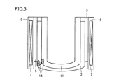
- the present inventors investigated each component member constituting the silicon purifier that caused the false detection. As a result of this investigation, as shown in FIG. 3, it was confirmed that the carbon or carbide 14 attached to the hot water leak detection sensor 5 was concentrated in the vicinity of the bottom of the silicon refining device. It was confirmed that the stamp material 3 was also attached to the periphery of the outer wall of the crucible 11 placed inside the stamp material 3. However, adhesion of carbon or carbide 14 was not confirmed around the inner wall of the crucible 11.
- the carbon or carbide (the portion 16 turned black) that existed at the bottom of the crucible 11 before use diffuses due to a thermal gradient when heated during silicon purification, and the outside of the crucible 11 It is conceivable that a phenomenon of sticking to the stamp material 3 or the sensor 5 occurs. From the above results, it was found that the crucible is made of alumina, but the carbon or carbide source is the crucible. And the organic binder containing a phenol resin etc. as a binder was used for the crucible provided in the apparatus in which the above misdetection of the hot water leak sensor generate
- the hot water leak detection sensor is arranged outside the outer wall of the crucible, and the hot water leak detection sensor detects a hot water leak by detecting a short circuit between the electrodes of the sensor.
- the hot water leak detection sensor detects a hot water leak by detecting a short circuit between the electrodes of the sensor.
- FIG. 1 is a cross-sectional view schematically showing an example of the configuration of a silicon purification apparatus according to the present invention.
- the silicon refining apparatus shown in FIG. 1 is configured to prevent erroneous detection of a sensor (sensor 5) that detects leakage of hot water from the crucible 1.
- a silicon refining device preferably further includes a stamp material 3, a heating device 7 and a coil cement 9 in addition to the crucible 1 and the sensor 5.
- the crucible 1 is for melting a silicon raw material in the crucible 1. Therefore, the crucible 1 only needs to be configured so as to be able to store a silicon raw material, and may have, for example, a recess 1a.
- the shape and size of the crucible 1 are not limited to the shape and size shown in FIG.
- the crucible 1 is made of an oxidation resistant material molded using a binder.
- “The crucible 1 is made of an oxidation-resistant material molded using a binder” means, for example, that the binder is mixed with alumina powder or mullite powder as a main component.
- a binder made of an inorganic material is used instead of a binder containing an organic material.
- the binder made of an inorganic material preferably has a low carbon content.
- the carbon content is preferably 10% by mass or less, and the closer the carbon content is to 0% by mass, the more preferable.
- the crucible 1 is manufactured using a binder made of an inorganic material, carbon leaks out of the crucible 1 during the purification of the silicon raw material, and the vicinity of the positive electrode 51 or the negative electrode 53 (see FIG. 2 below) of the sensor 5. As a result, it is possible to prevent an internal short circuit from occurring in the sensor 5. That is, if the crucible 1 is made using a binder made of an inorganic material, erroneous detection of the sensor 5 can be prevented.
- the inorganic material constituting the binder may be a ceramic material such as sodium silicate, potassium silicate or alumina sol, and may be a colloidal silica such as an anionic colloidal silica or a cationic colloidal silica. It may be an oxide sol such as zirconia sol, titania sol or alumina sol, or bentonite. It is good also as an inorganic material which mixes these and comprises a binder.
- the crucible 1 is preferably provided with a mechanism for taking out molten silicon from the crucible 1.
- FIG. 2 is a plan view schematically showing the configuration of the sensor 5 used in the silicon purification apparatus shown in FIG.
- the sensor 5 is a sensor for detecting a hot water leak from the crucible 1 as described above, and is provided outside the crucible 1.
- the configuration of the sensor 5 is not particularly limited.
- the sensor 5 only needs to be configured so that an internal short circuit occurs when silicon (molten silicon) leaking from the crucible 1 adheres.
- the sensor 5 may have the configuration shown in FIG.
- the 2 includes a positive electrode 51 and a negative electrode 53 fixed to a sheet base material 55.
- the positive electrode 51 may be made of a conductive material such as stainless steel, for example, and has a main body 51A and a plurality of terminal parts 51B extending from the main body 51A.
- the negative electrode 53 may be made of, for example, a conductive material such as stainless steel, and includes a main body portion 53A and a plurality of terminal portions 53B extending from the main body portion 53A.
- the terminal portions 51B are arranged at intervals
- the terminal portions 53B are also arranged at intervals
- the terminal portions 53B are arranged between the adjacent terminal portions 51B.
- the positive electrode 51 or the negative electrode 53 may be a nichrome wire.
- the sheet base material 55 can hold the sensor 5, is preferably insulative, and formed in a sheet shape, and may be a mica sheet made of, for example, mica.
- the main body 51 ⁇ / b> A of the positive electrode 51 and the positive terminal of the monitoring device are connected, the main body 53 ⁇ / b> A of the negative electrode 53 and the negative terminal of the monitoring device are connected, and the positive electrode 51 and the negative electrode 53 are connected.
- Monitor the current flowing through When the monitored current value exceeds the threshold value, it is determined that a hot water leak has occurred.
- the stamp material 3 is preferably provided between the crucible 1 and the sensor 5. Thereby, compared with the case where the stamp material 3 is not provided, the timing at which the molten silicon leaked from the crucible 1 reaches the coil cement 9 can be delayed. Therefore, even if carbon or carbide diffuses from the crucible 1, the timing of erroneous detection by the sensor 5 can be delayed. More preferably, the stamp material 3 is provided so that the distance between the outer wall of the crucible 1 and the sensor 5 is 20 mm or more and 100 mm or less.
- the stamp material 3 preferably has high fire resistance and high corrosion resistance, and is preferably made of particles having a particle size of 10 mm or less. Therefore, the material of the stamp material 3 is not particularly limited as long as it has high fire resistance and high corrosion resistance. For example, it may be alumina or magnesia.
- the heating device 7 only needs to be covered with the coil cement 9 and disposed outside the sensor 5, and any configuration can be used as long as the crucible 1 and the silicon raw material in the crucible 1 can be heated to the melting point of the silicon raw material or higher. You may have.
- the heating device may be a resistance heating device (heater heating device), or may be an induction heating device that arranges a coil on the outer periphery of the crucible 1 and performs heating by induction current.
- the material of the coil cement 9 is not particularly limited, and may be alumina, for example.
- the crucible 1 is made of an oxidation-resistant material molded using a binder made of an inorganic material, so that carbon or carbide is crucible during the purification of the silicon raw material. 1 can be prevented from diffusing. Therefore, erroneous detection of the sensor 5 can be prevented.
- the silicon purification method according to the present invention is performed using the silicon purification apparatus shown in FIG. Specifically, first, the silicon material is supplied into the recess 1 a of the crucible 1, and the silicon material is melted by the heating device 7. When the silicon raw material is melted, slag (for example, alkali metal oxide) is added into the recess 1 a of the crucible 1. As a result, boron in the silicon reacts with the slag, and the boron in the silicon is dissolved or taken into the slag and becomes a floating substance and exists on the surface of the silicon (molten silicon). By removing this suspended matter, the silicon raw material can be purified.
- slag for example, alkali metal oxide
- the silicon refining method according to the present invention it is preferable to perform a step of removing the suspended matter and then adding the slag again into the recess 1a of the crucible 1 to remove the produced suspended matter again. Thereby, high purity silicon is obtained. In order to increase the purity of the obtained silicon, it is preferable to repeatedly remove suspended matters and add slag.
- Example 1 the silicon raw material was purified using the silicon purification apparatus shown in FIG.
- the silicon refining device used in this example was provided with a crucible 1, a stamp material 3, a sensor 5, and a heating device 7 covered with coil cement 9.
- the crucible 1 used was a mixture of alumina powder and a binder made of an inorganic material.
- the stamp material 3 was made of alumina or magnesia, and consisted of particles having a particle size of 5 mm or less.
- the sensor 5 was the sensor shown in FIG. 2, and the heating device 7 was an induction heating device. The distance between the crucible 1 and the sensor 5 was 50 mm.
- a commercially available metal grade silicon raw material was supplied into the crucible 1. Thereafter, the silicon raw material in the crucible 1 was heated by the heating device 7. When the silicon raw material was melted, slag was added to the crucible 1. When suspended matter was generated on the surface of the molten silicon, this suspended matter was removed and the second purification was performed. That is, the alkali metal oxide was added again to the crucible 1 to remove the generated suspended matter. After removing the suspended matter 38 times, purified molten silicon was discharged. This series of steps was performed for 30 cycles. In this way, silicon was purified.
- Example 2 the silicon raw material was purified in accordance with the method described in Example 1 except that a crucible 1 formed by mixing a binder made of an inorganic material with mullite powder was used.
- the silicon raw material was purified according to the method described in Example 1 except that the crucible 1 was formed by mixing an organic binder containing a phenol resin with alumina powder.
- Example 1 and Example 2 the silicon raw material could be purified without stopping the purification work.
- the purification work was stopped due to erroneous detection of the sensor 5, so the purification work efficiency was lowered and the operating rate of the silicon purification apparatus was lowered.
Landscapes
- Chemical & Material Sciences (AREA)
- Organic Chemistry (AREA)
- Inorganic Chemistry (AREA)
- Silicon Compounds (AREA)
Abstract
シリコン原料を精製するためのシリコン精製装置は、シリコン原料を収納するための坩堝(1)と、溶融シリコンが坩堝(1)から漏れたことを検知するためのセンサ(5)とを備える。坩堝(1)は、無機材料からなるバインダを用いて成型された耐酸化性材料からなる。
Description
本発明は、シリコン精製装置およびシリコン精製方法に関する。
世界的な環境保護意識の高まりにより、再生可能エネルギー源としての太陽電池(とりわけ、シリコン系太陽電池)が注目されている。
太陽電池用原料シリコン(Solar Grade Silicon、以下では「SG-Si」と記すことがある)には、一般に純度が99.9999%(6N)以上で、比抵抗が0.5Ωcm以上のものが求められている。また、太陽電池の普及のさらなる拡大には、太陽電池の製造コストの低減が不可欠であり、太陽電池用シリコンを安価に製造するための技術が求められている。
このような背景の下、純度99%程度(低純度)の安価な金属級シリコン(Metallurgical Grade Silicon)から不純物を除去してSG-Siを得るという冶金的プロセスが各種提案されている。
たとえば特許文献1(特開平7-318256号公報)には、SG-Siを得るための冶金的プロセスに用いられる溶解炉ではないが、特殊鋼、鋳鋼、銅などの金属または合金の溶解に使用可能な高周波誘導溶解炉が記載されている。特許文献1に記載の溶解炉は、溶解される原料が入れられる坩堝と、坩堝を加熱するためのコイルと、コイルを被覆するコイルセメントと、坩堝とコイルセメントとの間に充填されたバックアップ材とを備えている。
また、特許文献2(特開2011-032138号公報)には、シリコンなどの単結晶または多結晶の結晶成長を行なうさいに原料融液の漏れを検出する漏洩検出方法が記載されており、具体的には原料を溶融させる坩堝を内包する炉の底部一面に検出手段が敷設された漏洩検出方法が記載されている。
さらに、特許文献3(特開2007-153693号公報)には、スラグ製錬法にて高純度シリコン製造する装置および製造方法が記載されている。特許文献3に記載された装置およびその製造方法では、直接誘導加熱手段への非通電時に溶融シリコンが坩堝内壁面と接触する領域が耐酸化性材料で形成されてなる坩堝を使用している。
特許文献1などに記載の溶解炉のバックアップ材とコイルセメントとの間に湯漏れ検知センサを設けた場合には、坩堝が破損した場合などに生じる湯漏れを検知することができる。しかし、アルミナ製坩堝またはムライト製坩堝が設けられた溶解炉を使用した場合に、湯漏れが発生していないにもかかわらず湯漏れ検知センサが湯漏れの発生を示す出力を行うことがあった。湯漏れ検知センサが湯漏れの発生を示す出力を行なうと、溶解炉の運転を停止して、作業者による湯漏れの有無の確認が必要となる。そのため、湯漏れ検知センサが誤検出(誤検出とは、湯漏れが発生していないにもかかわらず湯漏れが発生したと出力することである)すれば、溶解炉の稼動率の低下を招く。
耐酸化性材料からなる坩堝は、一般的には、鉄・鋼・銅・白金・銀・ニッケルなどの溶融に使用される。しかし、耐酸化性材料からなる坩堝を用いた場合における湯漏れセンサの誤検出に関しては、報告されていない。また、特許文献3には、耐酸化性材料からなる坩堝を使用することは記載されているが、その坩堝に含まれるバインダの材料については記載されていない。
本発明は、かかる点に鑑みてなされたものであり、その目的は、稼働率の低下を招くことなくシリコンを精製可能なシリコン精製装置およびシリコン精製方法の提供である。
本発明に係るシリコン精製装置は、シリコン原料を収納するための坩堝と、溶融シリコン(溶融されたシリコン)が坩堝から漏れたことを検知するためのセンサとを備える。坩堝は、無機材料からなるバインダを用いて成型された耐酸化性材料からなる。ここで、「シリコン原料」とは、純度99.999%(5N)未満のシリコンを意味する。
無機材料は、リン酸、水ガラス、セメント、セラミック、コロイダルシリカ、ヒュームドシリカ、酸化物ゾル、およびベントナイトの少なくとも1つであることが好ましい。
坩堝は、アルミナまたはムライトを主成分とした材料からなることが好ましい。ここで、「アルミナを主成分とした材料」は、アルミナ以外の材料が10質量%以下含まれていることを意味する。また、「ムライトを主成分とした材料」は、ムライト以外の材料が10質量%以下含まれていることを意味する。
坩堝とセンサとの間にスタンプ材が配置されていることが好ましい。
本発明に係るシリコン精製方法では、本発明に係るシリコン精製装置を用いてシリコン原料を精製する。
本発明に係るシリコン精製方法では、本発明に係るシリコン精製装置を用いてシリコン原料を精製する。
本発明に係るシリコン精製装置では、湯漏れ検知センサの誤検出を防止できるので、稼働率の低下を招くことなくシリコンを精製可能である。
本発明者らは、アルミナ製坩堝の外周に湯漏れ検知センサが設けられたシリコン精製装置を用いて、シリコン原料を精製することを試みた。本発明者らが用いた湯漏れ検知センサでは、電極間に流れる電流値が閾値を超えると、湯漏れが発生したと判断することができる。そこで、本発明者らは、シリコン原料の精製中、湯漏れ検知センサの電極間に流れる電流値をモニタリングした。すると、湯漏れ検知センサの電極間に流れる電流値が閾値を超えているにもかかわらず、つまり湯漏れ検知センサは湯漏れが発生していることを出力しているにもかかわらず、操業停止後に炉体を解体しても湯漏れ箇所を確認できない場合があることが分かった。この原因を探るべく誤検出を起こした湯漏れ検知センサの状態を調べたところ、黒色に変色した物質が湯漏れ検知センサの電極近傍に付着していることが分かった。黒色に変色した物質が付着している箇所にて湯漏れ検知センサにおける電極間の導通状態を確認したところ、短絡が発生していることを確認した。これらのことから、黒色に変色した物質は導電性の物質である炭素または炭化物と考えられ、この付着が原因となって、湯漏れ検知センサに流れる電流値が閾値を超えたものと考えられる。
次に、本発明者らは、湯漏れ検知センサの電極近傍に付着した炭素または炭化物の供給源を特定するため、誤検出を起こしたシリコン精製装置を構成する各構成部材を調査した。この調査の結果、図3に示すように、湯漏れ検知センサ5に付着した炭素または炭化物14は、シリコン精製装置の底部付近に集中して発生していることが確認され、センサ5の内側に配置されているスタンプ材3とスタンプ材3の内側に配置されている坩堝11の外壁周辺とにも付着していることが確認された。しかし、坩堝11の内壁周辺には、炭素または炭化物14の付着は確認されなかった。次に、未使用品の坩堝11の底部の外壁周辺を調査したところ、炭素または炭化物14の付着は確認されなかった。詳細に調査するため、未使用の坩堝11の底部を破壊しその断面を目視観察したところ、図4に示すように、坩堝11(白色)の内部に黒色に変色した部分16の存在を確認した。また、黒色に変色した部分16には導通性があることも確認出来たため、炭素または炭化物14が坩堝11の内部に存在しているものと考えられる。
確認された状況から、使用前に坩堝11の底部に存在していた炭素または炭化物(黒色に変色した部分16)が、シリコン精製中に加熱されることにより熱勾配によって拡散し、坩堝11の外側のスタンプ材3またはセンサ5などに付着する現象が発生していることが考えられる。以上の結果より、坩堝がアルミナ製であるにもかかわらず、炭素または炭化物の供給源が坩堝である可能性を見出した。そして、上記のような湯漏れセンサの誤検出が発生した装置に設けられた坩堝には、バインダとしてフェノール樹脂などを含む有機系バインダが用いられていた。これらの結果をまとめると、湯漏れ検知センサが坩堝の外壁よりも外側に配置されており、かつ、湯漏れ検知センサが当該センサの電極間の短絡を検出することにより湯漏れを検出するように構成されている場合、有機系バインダを含む坩堝を使用したときに誤検出が発生する可能性があるものと考えられる。この知見に基づいて、本発明を完成させた。
以下、本発明のシリコン精製装置およびシリコン精製方法について図面を用いて説明する。なお、本発明の図面において、同一の参照符号は、同一部分または相当部分を表すものである。また、長さ、幅、厚さ、深さなどの寸法関係は図面の明瞭化と簡略化のために適宜変更されており、実際の寸法関係を表すものではない。
<シリコン精製装置>
図1は、本発明に係るシリコン精製装置の構成の一例を模式的に示す断面図である。図1に示すシリコン精製装置は、坩堝1からの湯漏れを検知するセンサ(センサ5)の誤検出を防止可能なように構成されている。このようなシリコン精製装置は、坩堝1およびセンサ5以外に、スタンプ材3、加熱装置7およびコイルセメント9をさらに備えることが好ましい。
図1は、本発明に係るシリコン精製装置の構成の一例を模式的に示す断面図である。図1に示すシリコン精製装置は、坩堝1からの湯漏れを検知するセンサ(センサ5)の誤検出を防止可能なように構成されている。このようなシリコン精製装置は、坩堝1およびセンサ5以外に、スタンプ材3、加熱装置7およびコイルセメント9をさらに備えることが好ましい。
<坩堝>
坩堝1は、その内部においてシリコン原料を溶融させるものである。そのため、坩堝1はシリコン原料を収納可能に構成されていれば良く、たとえば凹部1aを有していれば良い。また、坩堝1の形状およびその大きさなどは図1に記載の形状および大きさなどに限定されない。
坩堝1は、その内部においてシリコン原料を溶融させるものである。そのため、坩堝1はシリコン原料を収納可能に構成されていれば良く、たとえば凹部1aを有していれば良い。また、坩堝1の形状およびその大きさなどは図1に記載の形状および大きさなどに限定されない。
坩堝1は、バインダを用いて成型された耐酸化性材料からなる。「坩堝1は、バインダを用いて成型された耐酸化性材料からなる」とは、たとえば、主成分であるアルミナ粉末又はムライト粉末にバインダを混ぜて成型されることを意味する。ここで、バインダとしては、有機材料を含むバインダではなく、無機材料からなるバインダを用いる。無機材料からなるバインダは、炭素含有率が低いものであることが好ましく、たとえば炭素含有率が10質量%以下であることが好ましく、炭素含有率が0質量%に近ければ近いほど好ましい。そのため、無機材料からなるバインダを用いて坩堝1を作製すれば、シリコン原料の精製時などにおいて、炭素が坩堝1から漏れ出してセンサ5の正極51または負極53(下記図2参照)の近傍に付着し、その結果、センサ5において内部短絡が発生することを防止できる。つまり、無機材料からなるバインダを用いて坩堝1を作製すれば、センサ5の誤検出を防止できる。
バインダを構成する無機材料は、珪酸ソーダ、珪酸カリまたはアルミナゾル等のセラミック材料であっても良く、アニオン性のコロイダルシリカまたはカチオン性のコロイダルシリカ等のコロイダルシリカであっても良く、ヒュームドシリカであっても良く、ジルコニアゾル、チタニアゾルまたはアルミナゾルなどの酸化物ゾルであっても良く、ベントナイトであっても良い。これらを混合してバインダを構成する無機材料としても良い。
なお、不図示であるが、坩堝1には、溶融シリコンを坩堝1から取り出すための機構が設けられていることが好ましい。
<センサ>
図2は、図1に示すシリコン精製装置に用いられるセンサ5の構成を模式的に示す平面図である。センサ5は、上述のように坩堝1からの湯漏れを検知するためのセンサであり、坩堝1の外側に設けられている。本発明では、センサ5の構成は特に限定されない。センサ5は、坩堝1から漏れたシリコン(溶融シリコン)が付着したときに内部短絡が発生するように構成されていれば良く、たとえば図2に示す構成を有していれば良い。
図2は、図1に示すシリコン精製装置に用いられるセンサ5の構成を模式的に示す平面図である。センサ5は、上述のように坩堝1からの湯漏れを検知するためのセンサであり、坩堝1の外側に設けられている。本発明では、センサ5の構成は特に限定されない。センサ5は、坩堝1から漏れたシリコン(溶融シリコン)が付着したときに内部短絡が発生するように構成されていれば良く、たとえば図2に示す構成を有していれば良い。
図2に示すセンサ5は、正極51と負極53とがシート基材55に固定されて構成されている。正極51は、たとえばステンレス鋼などの導電性材料からなれば良く、本体部51Aと、本体部51Aから延びる複数の端子部51Bとを有する。負極53は、たとえばステンレス鋼などの導電性材料からなれば良く、本体部53Aと、本体部53Aから延びる複数の端子部53Bとを有する。ここで、端子部51Bは互いに間隔を空けて配置されており、端子部53Bも互いに間隔を空けて配置されており、隣り合う端子部51Bの間に端子部53Bが配置されている。なお、正極51または負極53はニクロム線であっても良い。シート基材55は、センサ5を保持でき、絶縁性を有し、シート状に形成されていることが好ましく、たとえば雲母などからなるマイカシートであれば良い。
このようなセンサ5では、正極51の本体部51Aとモニター装置の正極端子とを接続し、負極53の本体部53Aとモニター装置の負極端子とを接続して、正極51と負極53との間に流れる電流をモニターする。そして、モニターされた電流値が閾値を超えると、湯漏れが発生していると判断される。
<スタンプ材>
スタンプ材3は、坩堝1とセンサ5との間に設けられていることが好ましい。これにより、スタンプ材3が設けられていない場合に比べて、坩堝1から漏れた溶融シリコンがコイルセメント9に到達するタイミングを遅らせることができる。よって、炭素または炭化物が坩堝1から拡散した場合であっても、センサ5での誤検出のタイミングを遅らせることができる。より好ましくは、坩堝1の外壁とセンサ5との距離が20mm以上100mm以下となるようにスタンプ材3を設けることである。スタンプ材3は、高耐火性および高耐蝕性などを有することが好ましく、粒径が10mm以下の粒子からなることが好ましい。そのため、スタンプ材3の材料は高耐火性および高耐蝕性などを有するのであれば特に限定されず、たとえばアルミナまたはマグネシアであれば良い。
スタンプ材3は、坩堝1とセンサ5との間に設けられていることが好ましい。これにより、スタンプ材3が設けられていない場合に比べて、坩堝1から漏れた溶融シリコンがコイルセメント9に到達するタイミングを遅らせることができる。よって、炭素または炭化物が坩堝1から拡散した場合であっても、センサ5での誤検出のタイミングを遅らせることができる。より好ましくは、坩堝1の外壁とセンサ5との距離が20mm以上100mm以下となるようにスタンプ材3を設けることである。スタンプ材3は、高耐火性および高耐蝕性などを有することが好ましく、粒径が10mm以下の粒子からなることが好ましい。そのため、スタンプ材3の材料は高耐火性および高耐蝕性などを有するのであれば特に限定されず、たとえばアルミナまたはマグネシアであれば良い。
<加熱装置(コイルセメント)>
加熱装置7は、コイルセメント9で被覆されてセンサ5の外側に配置されていれば良く、坩堝1および坩堝1内のシリコン原料をシリコン原料の融点以上に加熱できるのであればどのような構成を有していても良い。たとえば、加熱装置は、抵抗加熱装置(ヒーター加熱装置)であっても良いし、坩堝1の外周にコイルを配置して誘導電流による加熱を行う誘導加熱装置であっても良い。また、コイルセメント9の材料は特に限定されず、たとえばアルミナであれば良い。
加熱装置7は、コイルセメント9で被覆されてセンサ5の外側に配置されていれば良く、坩堝1および坩堝1内のシリコン原料をシリコン原料の融点以上に加熱できるのであればどのような構成を有していても良い。たとえば、加熱装置は、抵抗加熱装置(ヒーター加熱装置)であっても良いし、坩堝1の外周にコイルを配置して誘導電流による加熱を行う誘導加熱装置であっても良い。また、コイルセメント9の材料は特に限定されず、たとえばアルミナであれば良い。
以上説明したように、本発明に係るシリコン精製装置では、坩堝1は、無機材料からなるバインダを用いて成型された耐酸化性材料からなるため、シリコン原料の精製中などにおいて炭素または炭化物が坩堝1から拡散することを抑制できる。よって、センサ5の誤検出を防止することができる。
<シリコン精製方法>
本発明に係るシリコン精製方法は、図1に示すシリコン精製装置を用いて行なわれる。具体的には、まず、シリコン原料を坩堝1の凹部1a内に供給して、加熱装置7によりシリコン原料を溶融させる。シリコン原料が溶融したら、スラグ(たとえばアルカリ金属酸化物)を坩堝1の凹部1a内に添加する。これにより、シリコン中のボロンとスラグとが反応して、シリコン中のボロンがスラグに溶解または取り込まれて浮遊物となってシリコン(溶融シリコン)の表面に存在する。この浮遊物を除去すれば、シリコン原料を精製することができる。
本発明に係るシリコン精製方法は、図1に示すシリコン精製装置を用いて行なわれる。具体的には、まず、シリコン原料を坩堝1の凹部1a内に供給して、加熱装置7によりシリコン原料を溶融させる。シリコン原料が溶融したら、スラグ(たとえばアルカリ金属酸化物)を坩堝1の凹部1a内に添加する。これにより、シリコン中のボロンとスラグとが反応して、シリコン中のボロンがスラグに溶解または取り込まれて浮遊物となってシリコン(溶融シリコン)の表面に存在する。この浮遊物を除去すれば、シリコン原料を精製することができる。
なお、本発明に係るシリコン精製方法では、浮遊物を除去してから、上記スラグを坩堝1の凹部1a内に再び添加し、生じた浮遊物を再び除去するという工程を行なうことが好ましい。これにより、純度の高いシリコンが得られる。得られるシリコンの純度を高めるためには、浮遊物の除去とスラグの添加とを繰り返し行なうことが好ましい。
以下、実施例を挙げて本発明をより詳細に説明するが、本発明はこれらに限定されるものではない。
<実施例1>
実施例1では、図1に示すシリコン精製装置を用いてシリコン原料を精製した。本実施例で用いたシリコン精製装置には、坩堝1と、スタンプ材3と、センサ5と、コイルセメント9で被覆された加熱装置7とが設けられていた。坩堝1としては、アルミナ粉末に、無機材料からなるバインダを混ぜて成型されたものを用いた。スタンプ材3はアルミナまたはマグネシア製であり、粒径が5mm以下の粒子からなった。センサ5は図2に示すセンサであり、加熱装置7は誘導加熱装置であった。また、坩堝1とセンサ5との距離は50mmであった。
実施例1では、図1に示すシリコン精製装置を用いてシリコン原料を精製した。本実施例で用いたシリコン精製装置には、坩堝1と、スタンプ材3と、センサ5と、コイルセメント9で被覆された加熱装置7とが設けられていた。坩堝1としては、アルミナ粉末に、無機材料からなるバインダを混ぜて成型されたものを用いた。スタンプ材3はアルミナまたはマグネシア製であり、粒径が5mm以下の粒子からなった。センサ5は図2に示すセンサであり、加熱装置7は誘導加熱装置であった。また、坩堝1とセンサ5との距離は50mmであった。
まず、市販の金属級シリコン原料を坩堝1内に供給した。その後、加熱装置7によって坩堝1内のシリコン原料を加熱した。シリコン原料が溶融されると、スラグを坩堝1に添加した。溶融シリコンの表面に浮遊物が発生すると、この浮遊物を取り除き、2回目の精製を行なった。つまり、アルカリ金属酸化物を坩堝1に再度添加して、発生した浮遊物を除去した。浮遊物の除去を38回繰り返し行ったのち、精製された溶融シリコンを排出した。この一連の工程を30サイクル行った。このようにして、シリコンを精製した。
<実施例2>
実施例2では、坩堝1として無機材料からなるバインダをムライト粉末に混ぜて成型されたものを用いたことを除いては上記実施例1に記載の方法にしたがって、シリコン原料を精製した。
実施例2では、坩堝1として無機材料からなるバインダをムライト粉末に混ぜて成型されたものを用いたことを除いては上記実施例1に記載の方法にしたがって、シリコン原料を精製した。
<比較例>
比較例では、坩堝1としてフェノール樹脂を含む有機系バインダをアルミナ粉末に混ぜて成型されたものを用いたことを除いては上記実施例1に記載の方法にしたがって、シリコン原料を精製した。
比較例では、坩堝1としてフェノール樹脂を含む有機系バインダをアルミナ粉末に混ぜて成型されたものを用いたことを除いては上記実施例1に記載の方法にしたがって、シリコン原料を精製した。
<評価>
実施例1および2では、センサ5による誤検出なくシリコンを精製できたが、比較例では、センサ5が湯漏れを検出し操業を停止した。操業停止後に炉体を解体したが、湯漏れが確認できず、センサ5の誤検出であった。
実施例1および2では、センサ5による誤検出なくシリコンを精製できたが、比較例では、センサ5が湯漏れを検出し操業を停止した。操業停止後に炉体を解体したが、湯漏れが確認できず、センサ5の誤検出であった。
このように、実施例1および実施例2では、精製作業を停止することなくシリコン原料を精製できた。しかし、比較例では、センサ5の誤検出により精製作業を停止したため、精製作業効率が低下し、シリコン精製装置の稼働率が低下した。
今回開示された実施の形態および実施例はすべての点で例示であって制限的なものではないと考えられるべきである。本発明の範囲は上記した説明ではなくて請求の範囲によって示され、請求の範囲と均等の意味および範囲内でのすべての変更が含まれることが意図される。
1,11 坩堝、1a 凹部、3 スタンプ材、5 センサ、7 加熱装置、9 コイルセメント、14 炭素または炭化物、16 黒色に変色した部分、51 正極、51A,53A 本体部、51B,53B 端子部、53 負極、55 シート基材。
Claims (5)
- シリコン原料を精製するための装置であって、
前記シリコン原料を収納するための坩堝と、
溶融シリコンが前記坩堝から漏れたことを検知するためのセンサとを備え、
前記坩堝は、無機材料からなるバインダを用いて成型された耐酸化性材料からなるシリコン精製装置。 - 前記無機材料は、リン酸、水ガラス、セメント、セラミック、コロイダルシリカ、ヒュームドシリカ、酸化物ゾル、およびベントナイトの少なくとも1つである請求項1に記載のシリコン精製装置。
- 前記坩堝は、アルミナまたはムライトを主成分とした材料からなる請求項1または2に記載のシリコン精製装置。
- 前記坩堝と前記センサとの間にスタンプ材が配置されている請求項1~3のいずれかに記載のシリコン精製装置。
- 請求項1~4のいずれかに記載のシリコン精製装置を用いて前記シリコン原料を精製するシリコンの精製方法。
Applications Claiming Priority (2)
| Application Number | Priority Date | Filing Date | Title |
|---|---|---|---|
| JP2011266837 | 2011-12-06 | ||
| JP2011-266837 | 2011-12-06 |
Publications (1)
| Publication Number | Publication Date |
|---|---|
| WO2013084925A1 true WO2013084925A1 (ja) | 2013-06-13 |
Family
ID=48574283
Family Applications (1)
| Application Number | Title | Priority Date | Filing Date |
|---|---|---|---|
| PCT/JP2012/081485 Ceased WO2013084925A1 (ja) | 2011-12-06 | 2012-12-05 | シリコン精製装置およびシリコン精製方法 |
Country Status (1)
| Country | Link |
|---|---|
| WO (1) | WO2013084925A1 (ja) |
Cited By (1)
| Publication number | Priority date | Publication date | Assignee | Title |
|---|---|---|---|---|
| CN114538449A (zh) * | 2022-02-10 | 2022-05-27 | 贵州理工学院 | 一种用微硅粉为原料制备工业硅精炼渣剂的方法 |
Citations (3)
| Publication number | Priority date | Publication date | Assignee | Title |
|---|---|---|---|---|
| JPS6114364U (ja) * | 1984-06-29 | 1986-01-28 | 新日本製鐵株式会社 | 溶融金属の湯洩れ検出装置 |
| JPH11285777A (ja) * | 1998-04-02 | 1999-10-19 | Nissan Motor Co Ltd | 鋳型および鋳型の製作方法 |
| JP2009096644A (ja) * | 2007-10-12 | 2009-05-07 | Sharp Corp | シリコン精製方法およびシリコン精製装置 |
-
2012
- 2012-12-05 WO PCT/JP2012/081485 patent/WO2013084925A1/ja not_active Ceased
Patent Citations (3)
| Publication number | Priority date | Publication date | Assignee | Title |
|---|---|---|---|---|
| JPS6114364U (ja) * | 1984-06-29 | 1986-01-28 | 新日本製鐵株式会社 | 溶融金属の湯洩れ検出装置 |
| JPH11285777A (ja) * | 1998-04-02 | 1999-10-19 | Nissan Motor Co Ltd | 鋳型および鋳型の製作方法 |
| JP2009096644A (ja) * | 2007-10-12 | 2009-05-07 | Sharp Corp | シリコン精製方法およびシリコン精製装置 |
Cited By (1)
| Publication number | Priority date | Publication date | Assignee | Title |
|---|---|---|---|---|
| CN114538449A (zh) * | 2022-02-10 | 2022-05-27 | 贵州理工学院 | 一种用微硅粉为原料制备工业硅精炼渣剂的方法 |
Similar Documents
| Publication | Publication Date | Title |
|---|---|---|
| JP4850501B2 (ja) | 高純度シリコンの製造装置及び製造方法 | |
| EP3577402B1 (en) | Damage dectection system for refractory linings for molten metal containing vessels and method of use | |
| WO2013084925A1 (ja) | シリコン精製装置およびシリコン精製方法 | |
| JP5745588B2 (ja) | 誘導加熱炉用坩堝 | |
| CN202032557U (zh) | 立式锅炉超温保护装置 | |
| CN204240810U (zh) | 一种加热管 | |
| JP5963655B2 (ja) | 三相交流電極式円形電気炉及びその冷却方法 | |
| CN204138683U (zh) | 一种设有冷却壁的高炉出铁沟 | |
| CN202187089U (zh) | 快速反馈硅液溢流监控装置 | |
| KR101359061B1 (ko) | 측정프로브 | |
| KR20120077399A (ko) | 전기로 | |
| CN102829839B (zh) | 一种铸锻钢真空浇注欠浇高度检测装置 | |
| JPH09303971A (ja) | 誘導溶解炉の湯漏れ検出装置 | |
| CN208887801U (zh) | 直流电弧炉的炉底温度的测量系统 | |
| CN101706200B (zh) | 一种电弧炉耐火材料的养护方法及系统 | |
| TWI468521B (zh) | 高爐爐床狀況之判斷方法 | |
| CN103130224A (zh) | 多晶硅铸锭炉漏硅检测承接装置 | |
| CN203200351U (zh) | 一种铝电解槽侧部漏炉应急阻流封堵装置 | |
| CN202393518U (zh) | 一种用于真空系统的高温陶瓷热电偶 | |
| CN204718416U (zh) | 一种阳极炉口和烟道口钢水套 | |
| CN104613785B (zh) | 熔铝炉流槽口漏铝报警装置 | |
| CN1049044C (zh) | 一种直流电弧炉底电极 | |
| KR100829948B1 (ko) | 전기로의 연와파손 감지센서 장치 | |
| CN210322058U (zh) | 一种用于全电熔窑炉的液体温度检测设备 | |
| CN210208636U (zh) | 一种可实时显示厚度变化的透气砖 |
Legal Events
| Date | Code | Title | Description |
|---|---|---|---|
| 121 | Ep: the epo has been informed by wipo that ep was designated in this application |
Ref document number: 12855219 Country of ref document: EP Kind code of ref document: A1 |
|
| NENP | Non-entry into the national phase |
Ref country code: DE |
|
| 122 | Ep: pct application non-entry in european phase |
Ref document number: 12855219 Country of ref document: EP Kind code of ref document: A1 |
|
| NENP | Non-entry into the national phase |
Ref country code: JP |