WO2013082792A1 - 控制电路、lcd模块及lcd显示器 - Google Patents
控制电路、lcd模块及lcd显示器 Download PDFInfo
- Publication number
- WO2013082792A1 WO2013082792A1 PCT/CN2011/083720 CN2011083720W WO2013082792A1 WO 2013082792 A1 WO2013082792 A1 WO 2013082792A1 CN 2011083720 W CN2011083720 W CN 2011083720W WO 2013082792 A1 WO2013082792 A1 WO 2013082792A1
- Authority
- WO
- WIPO (PCT)
- Prior art keywords
- resistor
- lcd
- operational amplifier
- driver
- lcd panel
- Prior art date
- Legal status (The legal status is an assumption and is not a legal conclusion. Google has not performed a legal analysis and makes no representation as to the accuracy of the status listed.)
- Ceased
Links
Images


Classifications
-
- G—PHYSICS
- G09—EDUCATION; CRYPTOGRAPHY; DISPLAY; ADVERTISING; SEALS
- G09G—ARRANGEMENTS OR CIRCUITS FOR CONTROL OF INDICATING DEVICES USING STATIC MEANS TO PRESENT VARIABLE INFORMATION
- G09G3/00—Control arrangements or circuits, of interest only in connection with visual indicators other than cathode-ray tubes
- G09G3/20—Control arrangements or circuits, of interest only in connection with visual indicators other than cathode-ray tubes for presentation of an assembly of a number of characters, e.g. a page, by composing the assembly by combination of individual elements arranged in a matrix no fixed position being assigned to or needed to be assigned to the individual characters or partial characters
- G09G3/34—Control arrangements or circuits, of interest only in connection with visual indicators other than cathode-ray tubes for presentation of an assembly of a number of characters, e.g. a page, by composing the assembly by combination of individual elements arranged in a matrix no fixed position being assigned to or needed to be assigned to the individual characters or partial characters by control of light from an independent source
- G09G3/36—Control arrangements or circuits, of interest only in connection with visual indicators other than cathode-ray tubes for presentation of an assembly of a number of characters, e.g. a page, by composing the assembly by combination of individual elements arranged in a matrix no fixed position being assigned to or needed to be assigned to the individual characters or partial characters by control of light from an independent source using liquid crystals
- G09G3/3611—Control of matrices with row and column drivers
- G09G3/3685—Details of drivers for data electrodes
- G09G3/3688—Details of drivers for data electrodes suitable for active matrices only
-
- G—PHYSICS
- G09—EDUCATION; CRYPTOGRAPHY; DISPLAY; ADVERTISING; SEALS
- G09G—ARRANGEMENTS OR CIRCUITS FOR CONTROL OF INDICATING DEVICES USING STATIC MEANS TO PRESENT VARIABLE INFORMATION
- G09G2310/00—Command of the display device
- G09G2310/02—Addressing, scanning or driving the display screen or processing steps related thereto
- G09G2310/0264—Details of driving circuits
- G09G2310/0289—Details of voltage level shifters arranged for use in a driving circuit
-
- G—PHYSICS
- G09—EDUCATION; CRYPTOGRAPHY; DISPLAY; ADVERTISING; SEALS
- G09G—ARRANGEMENTS OR CIRCUITS FOR CONTROL OF INDICATING DEVICES USING STATIC MEANS TO PRESENT VARIABLE INFORMATION
- G09G2310/00—Command of the display device
- G09G2310/02—Addressing, scanning or driving the display screen or processing steps related thereto
- G09G2310/0264—Details of driving circuits
- G09G2310/0291—Details of output amplifiers or buffers arranged for use in a driving circuit
-
- G—PHYSICS
- G09—EDUCATION; CRYPTOGRAPHY; DISPLAY; ADVERTISING; SEALS
- G09G—ARRANGEMENTS OR CIRCUITS FOR CONTROL OF INDICATING DEVICES USING STATIC MEANS TO PRESENT VARIABLE INFORMATION
- G09G2320/00—Control of display operating conditions
- G09G2320/02—Improving the quality of display appearance
- G09G2320/0233—Improving the luminance or brightness uniformity across the screen
-
- G—PHYSICS
- G09—EDUCATION; CRYPTOGRAPHY; DISPLAY; ADVERTISING; SEALS
- G09G—ARRANGEMENTS OR CIRCUITS FOR CONTROL OF INDICATING DEVICES USING STATIC MEANS TO PRESENT VARIABLE INFORMATION
- G09G2320/00—Control of display operating conditions
- G09G2320/02—Improving the quality of display appearance
- G09G2320/0242—Compensation of deficiencies in the appearance of colours
Definitions
- the present invention relates to the field of LCD technologies, and in particular, to an LCD control circuit, an LCD module, and an LCD display.
- FIG. 1 is a multi-layer LCD control circuit used in the prior art.
- the channel traces of the respective outputs from the 3' to the LCD panel 4' adopt serpentine traces, so that the channel traces between the output terminals of the driver 3' and the LCD panel 4' can be realized.
- the module's LCD control circuit has been developed to use a high-speed driver drive architecture, so the wiring area between the output terminals of the driver and the LCD panel is limited, so that the output of the intermediate position of the driver is used between the LCD panel and the LCD panel.
- the serpentine traces are difficult to achieve the same length as the channel traces between the output terminals of the driver and the LCD panel, so that the channels between the outputs on the driver and the LCD panel are routed.
- the lengths are inconsistent, resulting in different impedances of the traces of the respective channels, and the voltages attenuated by the different impedances are different, resulting in inconsistent voltage deviations from the output terminals of the driver to the data lines of the LCD panel, thereby making the LCD panel
- the displayed color is biased, thereby affecting the visual effect of the image displayed on the LCD panel.
- a primary object of the present invention is to provide an LCD control circuit which is low in cost and which avoids color deviation in a display panel of an LCD panel.
- the present invention provides an LCD control circuit including a power supply, a controller, a driver, and an LCD panel.
- the power supply provides operating power to the LCD control circuit
- the driver is coupled to the controller and the Between the LCD panels, a voltage compensation circuit for compensating the output voltage of each output end of the driver is further connected between each output end of the driver and the LCD panel.
- the voltage compensation circuit includes a first resistor, a second resistor and an equivalent varistor circuit, wherein the first resistor and the second resistor are connected in series with each other and connected between a corresponding output end of the driver and the ground
- the input end of the equivalent varistor circuit is connected to the controller, and an output end of the equivalent varistor circuit is connected between the first resistor and the second resistor.
- the voltage compensation circuit further includes a first operational amplifier, a positive input terminal of the first operational amplifier is connected between the first resistor and the second resistor, and a negative input of the first operational amplifier The terminal is connected to the output of the first operational amplifier, and the output of the first operational amplifier is connected to the data line of the LCD panel.
- the equivalent varistor circuit comprises a digital sliding varistor, a third resistor, a second operational amplifier, an NMOS transistor and a fourth resistor, wherein the digital sliding varistor and the third resistor are connected in series to the power supply.
- the positive input terminal of the second operational amplifier is connected between the digital sliding rheostat and the third resistor
- the negative input terminal of the second operational amplifier and the source of the NMOS transistor are both Connected to the ground via the fourth resistor
- the output end of the second operational amplifier is connected to the gate of the NMOS transistor
- the drain of the NMOS transistor is connected to the first resistor and the second resistor between.
- the digital sliding rheostat is a 7-bit digital-to-analog converter with an I2C interface, and the I2C interface is connected to the controller.
- the invention also provides an LCD module, the LCD module comprising an LCD control circuit, the LCD control circuit comprising a power supply, a controller, a driver and an LCD panel, wherein the power supply provides working power for the LCD control circuit, a driver is connected between the controller and the LCD panel, and a voltage compensation circuit for compensating an output voltage of each output end of the driver is further connected between each output end of the driver and the LCD panel. .
- the invention also provides an LCD display comprising an LCD module, the LCD module comprising an LCD control circuit, the LCD control circuit comprising a power supply, a controller, a driver and an LCD panel, the power supply providing work for the LCD control circuit a power source, the driver is connected between the controller and the LCD panel, and an output voltage of each output end of the driver is respectively connected between each output end of the driver and the LCD panel. Voltage compensation circuit.
- a voltage compensation circuit for compensating the output voltage of each output end of the driver is respectively connected between each output end of the driver and the LCD panel in the LCD control circuit, so that the output voltage of each output end of the driver is made.
- the voltage values reaching the data lines of the LCD panel are consistent, thereby avoiding the color deviation caused by the display screen of the LCD panel, thereby improving the visual effect of the image displayed by the LCD panel, and solving the output terminals of the driver in the LCD control circuit to the LCD panel.
- 1 is a schematic structural view of a channel of a channel between each output end of the driver and the LCD panel when the LCD control circuit of the prior art adopts multiple drivers;
- FIG. 2 is a schematic structural view showing a channel trace between each output end of the driver and the LCD panel in the preferred embodiment of the LCD control circuit of the present invention
- FIG. 3 is a schematic diagram showing voltage waveforms of corresponding outputs of a driver in a preferred embodiment of the LCD control circuit of the present invention
- FIG. 4 is a circuit block diagram of a preferred embodiment of the LCD control circuit of the present invention.
- FIG. 5 is a schematic diagram showing the circuit structure of a voltage compensation circuit in a preferred embodiment of the LCD control circuit of the present invention.
- the main solution of the present invention is: by connecting a voltage compensation circuit for compensating the output voltage of each output end of the driver between each output end of the driver and the LCD panel in the LCD control circuit, so that the output voltage of each output end of the driver
- the voltage values reaching the data lines of the LCD panel are consistent to avoid the color deviation caused by the display of the LCD panel, thereby improving the visual effect of the image displayed by the LCD panel, and solving the output of the driver in the LCD control circuit to the LCD panel
- FIG. 2 is a schematic structural diagram of a channel trace between each output end of the driver and the LCD panel in the preferred embodiment of the LCD control circuit of the present invention, including a driver.
- LCD panel 4 and routing area 8 the output of the two sides of the driver 3 is the longest to the LCD panel 4, and the channel of the most intermediate output of the driver 3 to the LCD panel 4 is the shortest, that is, the driver.
- the lengths of the channel traces between the respective output terminals of the LCD panel 4 are inconsistent. If the lengths of the traces of the respective channels are inconsistent, the entire LCD panel 4 displays the same gray scale to avoid the display of the LCD panel 4. Color deviation, you must make the drive 3
- the output voltage of each output terminal is consistent with the voltage value of the data line of the LCD panel 4 after being routed through the corresponding channel.
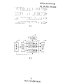
- FIG. 3 is a schematic diagram of voltage waveforms of corresponding outputs of a driver in a preferred embodiment of the LCD control circuit of the present invention, and a driver
- the output voltages corresponding to the four outputs on the left side of 3 are denoted as V1, V2, V3 and V4, respectively, where V1 represents the driver 3
- V4 represents the output voltage close to the most intermediate output terminal.
- the output voltage of the four output terminals of the driver is designed as V1>V2>V3>V4, the output voltages of the four output terminals of the driver are respectively After the attenuation of the corresponding channel trace between the driver and the LCD panel, the voltage value of the data line reaching the LCD panel can be made uniform, so that the entire LCD panel can display the same gray scale, thereby avoiding the display of the LCD panel. Color deviation.
- FIG. 4 is a circuit block diagram of a preferred embodiment of the LCD control circuit of the present invention, including a power supply 1, a controller 2, and a driver. 3. LCD panel 4, wherein a voltage compensation circuit 5 is connected to each output terminal of the driver 3.
- each voltage compensation circuit 5 for compensating the output voltage of each output terminal, each voltage compensation circuit 5 is also connected to the power supply source 1 and the controller 2, respectively, through the controller 2, the corresponding control data is written into each voltage compensation circuit 5, so that each voltage compensation circuit 5 performs corresponding voltage compensation on the output voltage of each output end of the driver 3, so that the driver 3
- the output voltage of each output reaches the voltage value of the data line of the LCD panel 4, thereby avoiding the color deviation caused by the display of the LCD panel 4, so as to improve the visual effect of the image displayed by the LCD panel 4.
- FIG. 5 is a schematic diagram of a circuit structure of a voltage compensation circuit in a preferred embodiment of the LCD control circuit of the present invention, including a first resistor R1, a second resistor R2, a first operational amplifier, and an equivalent varistor circuit 6, wherein
- the varistor circuit 6 includes a digital sliding varistor 7, a third resistor R3, a second operational amplifier, an NMOS transistor and a fourth resistor R4, and the digital sliding varistor 7 is a 7-bit digital-to-analog converter with an I2C interface, wherein the I2C interface string Row clock line and serial data line and controller in Figure 4 2 connections.
- the first resistor R1 and the second resistor R2 are connected in series to each other and connected to the driver. 3, between the corresponding output terminal and the ground, the input end of the equivalent varistor circuit 6 is connected to the output end of the controller 2, and the output end of the equivalent varistor circuit 6 is connected between the first resistor R1 and the second resistor R2.
- the positive input terminal of the first operational amplifier is connected between the first resistor R1 and the second resistor R2, and the negative input terminal of the first operational amplifier is connected to the output end of the first operational amplifier, and the output end of the first operational amplifier and the LCD panel Data line connection,
- the output voltage of the output of the first operational amplifier is the voltage outputted by the voltage compensation circuit 5 after the voltage output of the output voltage of the output of the driver 3 in FIG. 4, and the voltage after the compensation is passed through the driver.
- the corresponding channel traces between the LCD panel 4 and the LCD panel 4 are supplied to the data lines on the LCD panel 4.
- the digital-to-analog converter is connected in series with the third resistor R3 and connected between the power supply VDD and the ground, and the I2C interface of the digital-to-analog converter and the controller in FIG.
- the output terminal of the second operational amplifier is connected to the digital-to-analog converter, and the negative input terminal of the second operational amplifier and the source of the NMOS transistor are connected to the ground via the fourth resistor R4, and the second operational amplifier is The output end is connected to the gate of the NMOS transistor, and the drain of the NMOS transistor is connected between the first resistor R1 and the second resistor R2.
- the working principle of the voltage compensation circuit shown in Figure 4 is as follows: controller through the LCD control circuit 2 writing different control data to the digital-to-analog converter of each of the voltage compensation circuits 5, that is, writing different DAC code values, so that the voltage value input to the positive input terminal of the second operational amplifier in each voltage compensation circuit 5 Different, so that the degree of opening of the NMOS transistors in the voltage compensating circuits 5 is different, so that the current values flowing between the drain and the source of the NMOS transistors flowing through the voltage compensating circuits are different, that is, the current values of I in FIG. 5 are different.
- the voltage values outputted by the output terminals of the first operational amplifiers in the voltage compensating circuits 5 are different, that is, the voltage values of the output voltages of the output terminals of the first operational amplifier are different, that is, the controllers through the LCD control circuit. 2 to control the magnitude of the current in I of FIG. 5, thereby controlling the voltage level of the output voltage of the output of the first operational amplifier, so that the voltage outputted from each output of the driver 3 is driven by the driver.
- 3 and the LCD panel 4 have different lengths of channel traces and reach the same value of the voltage on the data line of the LCD panel 4, thereby avoiding the color deviation caused by the display of the LCD panel 4, and improving the visual image displayed by the LCD panel 4. Effect and solved the drive 3 The problem that the wiring area between each output terminal and the LCD panel 4 is limited.
- the present invention also provides an LCD module, which includes an LCD control circuit.
- the circuit structure of the LCD control circuit refers to the circuit structure of the LCD control circuit described in the above embodiments, and details are not described herein again.
- the present invention also provides an LCD display, which includes an LCD module, and the LCD module includes an LCD control circuit.
- the circuit structure of the LCD control circuit refers to the circuit structure of the LCD control circuit described in the above embodiments, and details are not described herein again.
- the invention has the beneficial effects that: in the LCD control circuit, a voltage compensation circuit for compensating the output voltage of each output end of the driver is respectively connected between each output end of the driver and the LCD panel, so that the output voltage of each output end of the driver reaches
- the voltage values of the data lines of the LCD panel are the same, which avoids the color deviation caused by the display screen of the LCD panel, thereby improving the visual effect of the image displayed by the LCD panel, and solving the difference between the output terminals of the driver in the LCD control circuit and the LCD panel.
- the problem that the routing area is limited, and the invention also has the advantages of simple structure and low cost.
Landscapes
- Engineering & Computer Science (AREA)
- Chemical & Material Sciences (AREA)
- Crystallography & Structural Chemistry (AREA)
- Physics & Mathematics (AREA)
- Computer Hardware Design (AREA)
- General Physics & Mathematics (AREA)
- Theoretical Computer Science (AREA)
- Control Of Indicators Other Than Cathode Ray Tubes (AREA)
- Liquid Crystal Display Device Control (AREA)
Abstract
一种LCD控制电路,其中LCD控制电路包括供电电源(1)、控制器(2)、驱动器(3)及LCD面板(4),供电电源(1)为该LCD控制电路提供工作电源,驱动器(3)连接于控制器(2)与LCD面板(4)之间,驱动器(3)的各输出端与LCD面板(4)之间还分别连接有一用于对驱动器(3)各输出端的输出电压进行补偿的电压补偿电路(5)。由此,避免了LCD面板显示画面所产生的色彩偏差,从而提高了该LCD面板(4)所显示图像的视觉效果,解决了LCD控制电路中驱动器(3)各输出端到LCD面板(4)之间走线区域有限的问题,并且还具有结构简单、成本低廉的优点。
Description
技术领域
本发明涉及LCD技术领域,尤其涉及一种LCD控制电路、LCD模块及LCD显示器。
背景技术
目前,
LCD驱动电路采用多颗驱动器的驱动架构时,为了避免LCD面板显示画面所产生的色彩偏差,通常是采用如图1所示的走线连接方式,图1是现有技术中LCD控制电路采用多颗驱动器时其驱动器各输出端到LCD面板的走线结构示意图,包括驱动器
3’和LCD面板4’,驱动器 3’与LCD面板4’连接时,在LCD面板4’上形成有走线区域8’,如图所示,驱动器
3’的各输出端到LCD面板4’之间的各通道走线采用蛇形走线,如此以来才能实现驱动器 3’各输出端到LCD面板4’之间的通道走线等长的目的,从而实现驱动器
3’各输出端的输出电压经驱动器
3’与LCD面板4’之间通道走线之后到达LCD面板4’数据线的电压值一致,从而达到避免LCD面板4’显示画面产生色彩偏差的目的。
然而,随着LCD技术的发展,目前中小尺寸LCD
模块的LCD控制电路已发展到采用1颗高速驱动器的驱动架构,因此供驱动器各输出端到LCD面板之间的走线区域很有限,使得驱动器上中间位置的输出端到LCD面板之间所采用的蛇形走线无论走得再密集也难以实现与该驱动器两边位置的输出端到LCD面板之间的通道走线等长,从而使得驱动器上各输出端到LCD面板之间的通道走线的长度不一致,从而导致各通道走线的阻抗不一样,又由于经过不同阻抗所衰减的电压不同,从而导致从驱动器各输出端到LCD面板数据线之间的电压偏差不一致,从而使得LCD面板上所显示出来的色彩产生偏差,从而影响该LCD面板所显示图像的视觉效果。
发明内容
本发明的主要目的是提供一种成本低且能避免LCD面板显示画面产生色彩偏差的LCD控制电路。
为了达到上述目的,本发明提出一种LCD控制电路,包括供电电源、控制器、驱动器及LCD面板,所述供电电源为该LCD控制电路提供工作电源,所述驱动器连接于所述控制器与所述LCD面板之间,所述驱动器的各输出端与所述LCD面板之间还分别连接有一用于对所述驱动器各输出端的输出电压进行补偿的电压补偿电路。
优选地,所述电压补偿电路包括第一电阻、第二电阻及一等效变阻器电路,所述第一电阻与所述第二电阻相互串联后连接于所述驱动器的相应输出端和地之间,所述等效变阻器电路的输入端与所述控制器连接,所述等效变阻器电路的输出端连接于所述第一电阻与所述第二电阻之间。
优选地,所述电压补偿电路还包括第一运算放大器,所述第一运算放大器的正极输入端连接于所述第一电阻与所述第二电阻之间,所述第一运算放大器的负极输入端与所述第一运算放大器的输出端连接,所述第一运算放大器的输出端与所述LCD面板的数据线连接。
优选地,所述等效变阻器电路包括数字滑动变阻器、第三电阻、第二运算放大器、NMOS管及第四电阻,所述数字滑动变阻器与所述第三电阻相互串联后连接于所述供电电源和地之间,所述第二运算放大器的正极输入端连接于所述数字滑动变阻器与所述第三电阻之间,所述第二运算放大器的负极输入端及所述NMOS管的源极均经所述第四电阻与地连接,所述第二运算放大器的输出端与所述NMOS管的栅极连接,所述NMOS管的漏极连接于所述第一电阻与所述第二电阻之间。
优选地,所述数字滑动变阻器为含I2C接口的7位数模转换器,所述I2C接口与所述控制器连接。
本发明还提出一种LCD模块,所述LCD模块包括LCD控制电路,所述LCD控制电路包括供电电源、控制器、驱动器及LCD面板,所述供电电源为该LCD控制电路提供工作电源,所述驱动器连接于所述控制器与所述LCD面板之间,所述驱动器的各输出端与所述LCD面板之间还分别连接有一用于对所述驱动器各输出端的输出电压进行补偿的电压补偿电路。
本发明还提出一种LCD显示器,包括LCD模块,所述LCD模块包括LCD控制电路,所述LCD控制电路包括供电电源、控制器、驱动器及LCD面板,所述供电电源为该LCD控制电路提供工作电源,所述驱动器连接于所述控制器与所述LCD面板之间,所述驱动器的各输出端与所述LCD面板之间还分别连接有一用于对所述驱动器各输出端的输出电压进行补偿的电压补偿电路。
本发明提出的LCD控制电路,由于在LCD控制电路中驱动器的各输出端与LCD面板之间分别连接有一用于对驱动器各输出端的输出电压进行补偿的电压补偿电路,使得驱动器各输出端的输出电压到达LCD面板数据线的电压值一致,避免了LCD面板显示画面所产生的色彩偏差,从而提高了该LCD面板所显示图像的视觉效果,且解决了LCD控制电路中驱动器各输出端到LCD面板之间走线区域有限的问题,并且本发明还具有结构简单、成本低廉的优点。
附图说明
图1是现有技术中LCD控制电路采用多颗驱动器时其驱动器各输出端到LCD面板之间通道走线的结构示意图;
图2是本发明LCD控制电路较佳实施例中驱动器各输出端到LCD面板之间通道走线的结构示意图;
图3是本发明LCD控制电路较佳实施例中驱动器相应输出端的电压波形示意图;
图4是本发明LCD控制电路较佳实施例的电路原理框图;
图5是本发明LCD控制电路较佳实施例中电压补偿电路的电路结构示意图。
本发明目的的实现、功能特点及优点将结合实施例,参照附图做进一步说明。
具体实施方式
本发明的主要解决方案是:通过在LCD控制电路中驱动器的各输出端与LCD面板之间分别连接一用于对驱动器各输出端的输出电压进行补偿的电压补偿电路,使得驱动器各输出端的输出电压到达LCD面板数据线的电压值一致,以避免LCD面板显示画面所产生的色彩偏差,从而提高该LCD面板所显示图像的视觉效果,并且解决了LCD控制电路中驱动器各输出端到LCD面板之间走线区域有限的问题。
参照图2,图2是本发明LCD控制电路较佳实施例中驱动器各输出端到LCD面板之间通道走线的结构示意图,包括驱动器
3、LCD面板4及走线区域8,驱动器 3最两边的输出端到LCD面板4的通道走线最长,驱动器 3最中间的输出端到LCD面板4的通道走线最短,即该驱动器
3的各个输出端到LCD面板4之间通道走线的长度不一致,若要在各通道走线长度不一致的情况下使整个LCD面板4显示同一个灰阶以避免LCD面板4显示画面所产生的色彩偏差,则必须使驱动器
3各输出端的输出电压经相应通道走线之后到达LCD面板4数据线的电压值一致。
参照图3,图3是本发明LCD控制电路较佳实施例中驱动器相应输出端的电压波形示意图,驱动器
3的左边四个输出端所对应的输出电压分别表示为V1、V2、V3及V4,其中V1代表驱动器
3最左边输出端的输出电压,V4代表靠近最中间输出端的输出电压,若将驱动器的该四个输出端的输出电压设计成V1>V2>V3>V4,则驱动器的该四个输出端的输出电压分别经驱动器与LCD面板之间相应通道走线的衰减后,可以实现其到达LCD面板数据线的电压值一致,即可实现使整个LCD面板显示同一个灰阶,从而避免LCD面板显示画面所产生的色彩偏差。
参照图4,图4是本发明LCD控制电路较佳实施例的电路原理框图,包括供电电源1、控制器 2、驱动器
3、LCD面板4,其中在驱动器 3的各输出端均连接有一电压补偿电路5。
具体的,在驱动器 3的各输出端与LCD面板4之间分别连接一用于对驱动器
3各输出端的输出电压进行补偿的电压补偿电路5,各电压补偿电路5还分别与供电电源1及控制器 2连接,通过控制器
2往各电压补偿电路5中写入相应的控制数据,使得各电压补偿电路5对驱动器 3各输出端的输出电压进行相应的电压补偿,使得驱动器
3各输出端的输出电压到达LCD面板4数据线的电压值一致,从而避免了LCD面板4显示画面所产生的色彩偏差,以提高LCD面板4所显示图像的视觉效果。
参照图5,图5是本发明LCD控制电路较佳实施例中电压补偿电路的电路结构示意图,包括第一电阻R1、第二电阻R2、第一运算放大器及一等效变阻器电路6,其中等效变阻器电路6包括数字滑动变阻器7、第三电阻R3、第二运算放大器、NMOS管及第四电阻R4,而数字滑动变阻器7为含I2C接口的7位数模转换器,其中I2C接口的串行时钟线及串行数据线与图4中的控制器
2连接。
具体的,第一电阻R1与第二电阻R2相互串联后连接于驱动器
3相应的输出端和地之间,等效变阻器电路6的输入端连接于控制器 2的输出端,等效变阻器电路6的输出端连接于第一电阻R1与第二电阻R2之间。
第一运算放大器的正极输入端连接于第一电阻R1与第二电阻R2之间,第一运算放大器的负极输入端与第一运算放大器的输出端连接,第一运算放大器的输出端与LCD面板的数据线连接,
第一运算放大器输出端的输出电压即图4中驱动器 3输出端的输出电压经电压补偿电路5进行电压补偿之后所输出的电压,该补偿之后的电压经驱动器
3与LCD面板4之间相应的通道走线输送给LCD面板4上的数据线。
数模转换器与第三电阻R3串联后连接于供电电源VDD和地之间,数模转换器的I2C接口与图4中的控制器
2的输出端连接,第二运算放大器的正极输入端与数模转换器连接,第二运算放大器的负极输入端及NMOS管的源极均经第四电阻R4与地连接,第二运算放大器的输出端与NMOS管的栅极连接,NMOS管的漏极连接于第一电阻R1与第二电阻R2之间。
图4所示电压补偿电路的工作原理如下:通过LCD控制电路的控制器
2往其各电压补偿电路5的数模转换器中写入不同的控制数据,即写入不同的DAC码值,使得各电压补偿电路5中第二运算放大器的正极输入端所输入的电压值不同,从而使得各电压补偿电路5中NMOS管的打开程度不同,从而使得流过各电压补偿电路中NMOS管的漏极和源极之间的电流值不同,即图5中I的电流值不同,从而使得各电压补偿电路5中第一运算放大器输出端所输出的电压值不同,即图中第一运算放大器输出端的输出电压的电压值不同,也即通过LCD控制电路的控制器
2来控制图5中I的电流大小,从而控制第一运算放大器输出端的输出电压的电压大小,从而使得驱动器 3各输出端所输出的电压经驱动器
3和LCD面板4之间不同长度的通道走线之后到达LCD面板4数据线上的电压值一致,从而避免了LCD面板4显示画面所产生的色彩偏差,提高了LCD面板4所显示图像的视觉效果,并且解决了驱动器
3各输出端到LCD面板4之间走线区域有限的问题。
本发明还提出一种LCD模块,该LCD模块包括LCD控制电路,其LCD控制电路的电路结构参照上面实施例所述的LCD控制电路的电路结构,此处不再赘述。
本发明还提出一种LCD显示器,该LCD显示器包括LCD模块,其LCD模块包括LCD控制电路,LCD控制电路的电路结构参照上面实施例所述的LCD控制电路的电路结构,此处不再赘述。
本发明的有益效果是:由于在LCD控制电路中驱动器的各输出端与LCD面板之间分别连接有一用于对驱动器各输出端的输出电压进行补偿的电压补偿电路,使得驱动器各输出端的输出电压到达LCD面板数据线的电压值一致,避免了LCD面板显示画面所产生的色彩偏差,从而提高了该LCD面板所显示图像的视觉效果,且解决了LCD控制电路中驱动器各输出端到LCD面板之间走线区域有限的问题,并且本发明还具有结构简单、成本低廉的优点。
以上所述仅为本发明的优选实施例,并非因此限制本发明的专利范围,凡是利用本发明说明书及附图内容所作的等效结构或等效流程变换,或直接或间接运用在其他相关的技术领域,均同理包括在本发明的专利保护范围内。
Claims (15)
- 一种LCD控制电路,包括供电电源、控制器、驱动器及LCD面板,所述供电电源为该LCD控制电路提供工作电源,所述驱动器连接于所述控制器与所述LCD面板之间,其特征在于:所述驱动器的各输出端与所述LCD面板之间还分别连接有一用于对所述驱动器各输出端的输出电压进行补偿的电压补偿电路。
- 根据权利要求1所述的LCD控制电路,其特征在于,所述电压补偿电路包括第一电阻、第二电阻及一等效变阻器电路,所述第一电阻与所述第二电阻相互串联后连接于所述驱动器的相应输出端和地之间,所述等效变阻器电路的输入端与所述控制器连接,所述等效变阻器电路的输出端连接于所述第一电阻与所述第二电阻之间。
- 根据权利要求2所述的LCD控制电路,其特征在于,所述电压补偿电路还包括第一运算放大器,所述第一运算放大器的正极输入端连接于所述第一电阻与所述第二电阻之间,所述第一运算放大器的负极输入端与所述第一运算放大器的输出端连接,所述第一运算放大器的输出端与所述LCD面板的数据线连接。
- 根据权利要求2所述的LCD控制电路,其特征在于,所述等效变阻器电路包括数字滑动变阻器、第三电阻、第二运算放大器、NMOS管及第四电阻,所述数字滑动变阻器与所述第三电阻相互串联后连接于所述供电电源和地之间,所述第二运算放大器的正极输入端连接于所述数字滑动变阻器与所述第三电阻之间,所述第二运算放大器的负极输入端及所述NMOS管的源极均经所述第四电阻与地连接,所述第二运算放大器的输出端与所述NMOS管的栅极连接,所述NMOS管的漏极连接于所述第一电阻与所述第二电阻之间。
- 根据权利要求4所述的LCD控制电路,其特征在于,所述数字滑动变阻器为含I2C接口的7位数模转换器,所述I2C接口与所述控制器连接。
- 一种LCD模块,包括LCD控制电路,所述LCD控制电路包括供电电源、控制器、驱动器及LCD面板,所述供电电源为该LCD控制电路提供工作电源,所述驱动器连接于所述控制器与所述LCD面板之间,其特征在于:所述驱动器的各输出端与所述LCD面板之间还分别连接有一用于对所述驱动器各输出端的输出电压进行补偿的电压补偿电路。
- 根据权利要求6所述的LCD模块,其特征在于,所述电压补偿电路包括第一电阻、第二电阻及一等效变阻器电路,所述第一电阻与所述第二电阻相互串联后连接于所述驱动器的相应输出端和地之间,所述等效变阻器电路的输入端与所述控制器连接,所述等效变阻器电路的输出端连接于所述第一电阻与所述第二电阻之间。
- 根据权利要求7所述的LCD模块,其特征在于,所述电压补偿电路还包括第一运算放大器,所述第一运算放大器的正极输入端连接于所述第一电阻与所述第二电阻之间,所述第一运算放大器的负极输入端与所述第一运算放大器的输出端连接,所述第一运算放大器的输出端与所述LCD面板的数据线连接。
- 根据权利要求7所述的LCD模块,其特征在于,所述等效变阻器电路包括数字滑动变阻器、第三电阻、第二运算放大器、NMOS管及第四电阻,所述数字滑动变阻器与所述第三电阻相互串联后连接于所述供电电源和地之间,所述第二运算放大器的正极输入端连接于所述数字滑动变阻器与所述第三电阻之间,所述第二运算放大器的负极输入端及所述NMOS管的源极均经所述第四电阻与地连接,所述第二运算放大器的输出端与所述NMOS管的栅极连接,所述NMOS管的漏极连接于所述第一电阻与所述第二电阻之间。
- 根据权利要求9所述的LCD模块,其特征在于,所述数字滑动变阻器为含I2C接口的7位数模转换器,所述I2C接口与所述控制器连接。
- 一种LCD显示器,包括LCD模块,所述LCD模块包括LCD控制电路,所述LCD控制电路包括供电电源、控制器、驱动器及LCD面板,所述供电电源为该LCD控制电路提供工作电源,所述驱动器连接于所述控制器与所述LCD面板之间,其特征在于:所述驱动器的各输出端与所述LCD面板之间还分别连接有一用于对所述驱动器各输出端的输出电压进行补偿的电压补偿电路。
- 根据权利要求11所述的LCD显示器,其特征在于,所述电压补偿电路包括第一电阻、第二电阻及一等效变阻器电路,所述第一电阻与所述第二电阻相互串联后连接于所述驱动器的相应输出端和地之间,所述等效变阻器电路的输入端与所述控制器连接,所述等效变阻器电路的输出端连接于所述第一电阻与所述第二电阻之间。
- 根据权利要求12所述的LCD显示器,其特征在于,所述电压补偿电路还包括第一运算放大器,所述第一运算放大器的正极输入端连接于所述第一电阻与所述第二电阻之间,所述第一运算放大器的负极输入端与所述第一运算放大器的输出端连接,所述第一运算放大器的输出端与所述LCD面板的数据线连接。
- 根据权利要求12所述的LCD显示器,其特征在于,所述等效变阻器电路包括数字滑动变阻器、第三电阻、第二运算放大器、NMOS管及第四电阻,所述数字滑动变阻器与所述第三电阻相互串联后连接于所述供电电源和地之间,所述第二运算放大器的正极输入端连接于所述数字滑动变阻器与所述第三电阻之间,所述第二运算放大器的负极输入端及所述NMOS管的源极均经所述第四电阻与地连接,所述第二运算放大器的输出端与所述NMOS管的栅极连接,所述NMOS管的漏极连接于所述第一电阻与所述第二电阻之间。
- 根据权利要求14所述的LCD显示器,其特征在于,所述数字滑动变阻器为含I2C接口的7位数模转换器,所述I2C接口与所述控制器连接。
Priority Applications (1)
| Application Number | Priority Date | Filing Date | Title |
|---|---|---|---|
| US13/380,069 US8704816B2 (en) | 2011-12-07 | 2011-08-12 | Control circuit for adjusting an initial value of a driving voltage being transferred to a liquid crystal panel |
Applications Claiming Priority (2)
| Application Number | Priority Date | Filing Date | Title |
|---|---|---|---|
| CN201120505521.4U CN202394505U (zh) | 2011-12-07 | 2011-12-07 | Lcd控制电路及lcd模块 |
| CN201120505521.4 | 2011-12-07 |
Publications (1)
| Publication Number | Publication Date |
|---|---|
| WO2013082792A1 true WO2013082792A1 (zh) | 2013-06-13 |
Family
ID=46669412
Family Applications (1)
| Application Number | Title | Priority Date | Filing Date |
|---|---|---|---|
| PCT/CN2011/083720 Ceased WO2013082792A1 (zh) | 2011-12-07 | 2011-12-08 | 控制电路、lcd模块及lcd显示器 |
Country Status (3)
| Country | Link |
|---|---|
| US (1) | US8704816B2 (zh) |
| CN (1) | CN202394505U (zh) |
| WO (1) | WO2013082792A1 (zh) |
Cited By (1)
| Publication number | Priority date | Publication date | Assignee | Title |
|---|---|---|---|---|
| US10319285B2 (en) | 2016-06-03 | 2019-06-11 | Boe Technology Group Co., Ltd. | Panel drive device and display device |
Families Citing this family (3)
| Publication number | Priority date | Publication date | Assignee | Title |
|---|---|---|---|---|
| CN103117050B (zh) * | 2013-02-05 | 2016-06-08 | 深圳市华星光电技术有限公司 | 用于液晶显示器的补偿电路及液晶显示器 |
| CN104123920A (zh) * | 2013-07-29 | 2014-10-29 | 深超光电(深圳)有限公司 | 液晶显示装置及其栅极驱动器 |
| CN104537990A (zh) | 2014-12-24 | 2015-04-22 | 深圳市华星光电技术有限公司 | 提高显示图像均匀性的方法及装置 |
Citations (6)
| Publication number | Priority date | Publication date | Assignee | Title |
|---|---|---|---|---|
| JP2001042834A (ja) * | 1999-07-30 | 2001-02-16 | Hitachi Ltd | 液晶表示装置 |
| US20020047557A1 (en) * | 2000-03-13 | 2002-04-25 | Jong-Seon Kim | Driving apparatus of a flat panel display |
| TW200737064A (en) * | 2006-03-16 | 2007-10-01 | Princeton Technology Corp | Display control system of a display device and control method thereof |
| TW200813930A (en) * | 2006-09-07 | 2008-03-16 | Au Optronics Corp | Display device and method capable of adjusting slew rate |
| CN101266759A (zh) * | 2007-03-13 | 2008-09-17 | 奇美电子股份有限公司 | 显示面板 |
| CN101398584A (zh) * | 2007-09-27 | 2009-04-01 | 北京京东方光电科技有限公司 | 液晶显示装置驱动方法 |
Family Cites Families (4)
| Publication number | Priority date | Publication date | Assignee | Title |
|---|---|---|---|---|
| JP4543725B2 (ja) * | 2004-03-30 | 2010-09-15 | セイコーエプソン株式会社 | 表示装置 |
| TWI325130B (en) * | 2006-01-12 | 2010-05-21 | Himax Display Inc | Led current driving system for lcos display |
| KR20080077495A (ko) * | 2007-02-20 | 2008-08-25 | 삼성전자주식회사 | 회로 기판 및 이를 포함하는 액정 표시 장치 |
| US8384634B2 (en) * | 2008-09-24 | 2013-02-26 | Apple Inc. | Display with reduced parasitic effects |
-
2011
- 2011-08-12 US US13/380,069 patent/US8704816B2/en active Active
- 2011-12-07 CN CN201120505521.4U patent/CN202394505U/zh not_active Expired - Lifetime
- 2011-12-08 WO PCT/CN2011/083720 patent/WO2013082792A1/zh not_active Ceased
Patent Citations (6)
| Publication number | Priority date | Publication date | Assignee | Title |
|---|---|---|---|---|
| JP2001042834A (ja) * | 1999-07-30 | 2001-02-16 | Hitachi Ltd | 液晶表示装置 |
| US20020047557A1 (en) * | 2000-03-13 | 2002-04-25 | Jong-Seon Kim | Driving apparatus of a flat panel display |
| TW200737064A (en) * | 2006-03-16 | 2007-10-01 | Princeton Technology Corp | Display control system of a display device and control method thereof |
| TW200813930A (en) * | 2006-09-07 | 2008-03-16 | Au Optronics Corp | Display device and method capable of adjusting slew rate |
| CN101266759A (zh) * | 2007-03-13 | 2008-09-17 | 奇美电子股份有限公司 | 显示面板 |
| CN101398584A (zh) * | 2007-09-27 | 2009-04-01 | 北京京东方光电科技有限公司 | 液晶显示装置驱动方法 |
Cited By (1)
| Publication number | Priority date | Publication date | Assignee | Title |
|---|---|---|---|---|
| US10319285B2 (en) | 2016-06-03 | 2019-06-11 | Boe Technology Group Co., Ltd. | Panel drive device and display device |
Also Published As
| Publication number | Publication date |
|---|---|
| US20130038638A1 (en) | 2013-02-14 |
| CN202394505U (zh) | 2012-08-22 |
| US8704816B2 (en) | 2014-04-22 |
Similar Documents
| Publication | Publication Date | Title |
|---|---|---|
| CN103730085B (zh) | 显示装置 | |
| WO2016201728A1 (zh) | 显示面板及其驱动方法 | |
| TWI570680B (zh) | 源極驅動器及更新伽瑪曲線的方法 | |
| WO2015058433A1 (zh) | 面板检测装置及显示面板 | |
| KR101931248B1 (ko) | 표시장치 및 그 제조방법 | |
| WO2017049688A1 (zh) | 一种goa电路及其驱动方法、液晶显示器 | |
| WO2016161679A1 (zh) | 一种goa电路及液晶显示器 | |
| WO2017015989A1 (zh) | 基板电路及显示面板 | |
| CN101398584A (zh) | 液晶显示装置驱动方法 | |
| WO2014056239A1 (zh) | 液晶显示装置及其驱动电路 | |
| WO2016041241A1 (zh) | 一种源极驱动电路及显示装置 | |
| WO2017215049A1 (zh) | 一种液晶显示面板的走线结构及其制作方法 | |
| WO2020134970A1 (zh) | 驱动电路、显示面板驱动装置和显示装置 | |
| WO2013082792A1 (zh) | 控制电路、lcd模块及lcd显示器 | |
| CN112967678B (zh) | 显示面板和电子设备 | |
| WO2017028350A1 (zh) | 液晶显示装置及其goa扫描电路 | |
| WO2018176561A1 (zh) | 一种液晶面板驱动电路及液晶显示装置 | |
| WO2020056892A1 (zh) | 阻抗差异补偿电路、显示面板及移动终端 | |
| WO2021203778A1 (zh) | 显示装置、显示系统 | |
| WO2017101176A1 (zh) | 液晶显示装置 | |
| KR20080041089A (ko) | 액정표시장치와 그 구동방법 | |
| WO2013181860A1 (zh) | 显示面板、平板显示装置及其驱动方法 | |
| WO2018113008A1 (zh) | 显示面板及显示装置 | |
| WO2017219399A1 (zh) | 显示驱动电路及液晶显示面板 | |
| WO2018157419A1 (zh) | 驱动电路及液晶显示装置 |
Legal Events
| Date | Code | Title | Description |
|---|---|---|---|
| WWE | Wipo information: entry into national phase |
Ref document number: 13380069 Country of ref document: US |
|
| 121 | Ep: the epo has been informed by wipo that ep was designated in this application |
Ref document number: 11876987 Country of ref document: EP Kind code of ref document: A1 |
|
| NENP | Non-entry into the national phase |
Ref country code: DE |
|
| 122 | Ep: pct application non-entry in european phase |
Ref document number: 11876987 Country of ref document: EP Kind code of ref document: A1 |