WO2013077057A1 - 太陽電池モジュールの絶縁検査用プローブ、太陽電池モジュールの絶縁検査方法、および太陽電池モジュールの製造方法 - Google Patents
太陽電池モジュールの絶縁検査用プローブ、太陽電池モジュールの絶縁検査方法、および太陽電池モジュールの製造方法 Download PDFInfo
- Publication number
- WO2013077057A1 WO2013077057A1 PCT/JP2012/072583 JP2012072583W WO2013077057A1 WO 2013077057 A1 WO2013077057 A1 WO 2013077057A1 JP 2012072583 W JP2012072583 W JP 2012072583W WO 2013077057 A1 WO2013077057 A1 WO 2013077057A1
- Authority
- WO
- WIPO (PCT)
- Prior art keywords
- solar cell
- cell module
- probe
- insulation
- insulation inspection
- Prior art date
- Legal status (The legal status is an assumption and is not a legal conclusion. Google has not performed a legal analysis and makes no representation as to the accuracy of the status listed.)
- Ceased
Links
Images




Classifications
-
- G—PHYSICS
- G01—MEASURING; TESTING
- G01R—MEASURING ELECTRIC VARIABLES; MEASURING MAGNETIC VARIABLES
- G01R1/00—Details of instruments or arrangements of the types included in groups G01R5/00 - G01R13/00 and G01R31/00
- G01R1/02—General constructional details
- G01R1/06—Measuring leads; Measuring probes
- G01R1/067—Measuring probes
- G01R1/06711—Probe needles; Cantilever beams; "Bump" contacts; Replaceable probe pins
- G01R1/06733—Geometry aspects
- G01R1/06738—Geometry aspects related to tip portion
-
- H—ELECTRICITY
- H02—GENERATION; CONVERSION OR DISTRIBUTION OF ELECTRIC POWER
- H02S—GENERATION OF ELECTRIC POWER BY CONVERSION OF INFRARED RADIATION, VISIBLE LIGHT OR ULTRAVIOLET LIGHT, e.g. USING PHOTOVOLTAIC [PV] MODULES
- H02S50/00—Monitoring or testing of PV systems, e.g. load balancing or fault identification
- H02S50/10—Testing of PV devices, e.g. of PV modules or single PV cells
-
- Y—GENERAL TAGGING OF NEW TECHNOLOGICAL DEVELOPMENTS; GENERAL TAGGING OF CROSS-SECTIONAL TECHNOLOGIES SPANNING OVER SEVERAL SECTIONS OF THE IPC; TECHNICAL SUBJECTS COVERED BY FORMER USPC CROSS-REFERENCE ART COLLECTIONS [XRACs] AND DIGESTS
- Y02—TECHNOLOGIES OR APPLICATIONS FOR MITIGATION OR ADAPTATION AGAINST CLIMATE CHANGE
- Y02E—REDUCTION OF GREENHOUSE GAS [GHG] EMISSIONS, RELATED TO ENERGY GENERATION, TRANSMISSION OR DISTRIBUTION
- Y02E10/00—Energy generation through renewable energy sources
- Y02E10/50—Photovoltaic [PV] energy
Definitions
- the present invention relates to a solar cell module insulation inspection probe, a solar cell module insulation inspection method using the inspection probe, and a solar cell module manufacturing method.
- a solar cell generates electromotive force between a positive electrode and a negative electrode of a photoelectric conversion element by making light such as sunlight enter a photoelectric conversion element using a semiconductor material.
- solar cells are often installed outdoors, and are generally installed as solar cell modules in which photoelectric conversion elements are sealed.
- FIG. 12A and 12B show the structure of the solar cell module disclosed in Patent Document 1 (Japanese Patent Laid-Open No. 2010-165749).
- Fig.12 (a) shows the surface side of a solar cell module
- FIG.12 (b) shows the back surface side of a solar cell module.
- the solar cell module 200 consists of many photovoltaic cells 201 connected in series, and the support frame 202 made from a frame shape aluminum.
- the support frame 202 supports a structure that protects the solar battery cell 201 with a front cover member with high translucency, a back cover member 203 with excellent weather resistance, and a resin encapsulated therebetween.
- the terminal box device 205 is attached to the back cover member 203 and constitutes the output part of the solar cell module 200.
- a module connection cable 204 extending to another solar cell module 200 is connected to the terminal box device 205.
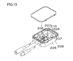
- FIG. 13 shows a terminal box constituting the output part of the solar cell disclosed in Patent Document 2 (Japanese Patent Laid-Open No. 2001-168368).
- a terminal box device 205 for a solar cell includes a plurality of relay terminals 207 provided with connecting portions 210 inside a casing 208 having an insertion port 209 through which an output electrode material for solar cells is inserted, and relays thereof. This constitutes the output part of the solar cell module in which the thin bare chip 206 as a bypass diode connected to the terminal 207 is disposed.
- Patent Document 2 discloses that the output extraction electrode material is electrically connected to the connection portion 210 by a joining means such as soldering.
- the solar cell module is required to have an insulation performance between the photoelectric conversion element and the peripheral member so that no leakage occurs even if it is struck by rain outdoors. Therefore, it is necessary to perform an insulation test in order to ensure the reliability of the solar cell module.
- Insulation inspection methods include, for example, IEC 61646, which is one of the international standards for thin film solar cell modules, and IEC 61215, which is one of the international standards for crystalline solar cell modules, and metals such as peripheral frames of photoelectric conversion elements and solar cell modules. It is specified that an insulation test is performed by applying a voltage between the two parts.
- the module connection cable 204 which is one of the parts constituting the output portion of the solar cell 201, and an aluminum support A voltage is applied between the frame 202 and an insulation test is performed.
- the connecting cable of the solar cell module is generally a connector at the tip, and it is necessary to insert a probe when applying a voltage and to remove the probe after applying the voltage.
- the cable is flexible and easy to move and is difficult to grab with a machine. Therefore, it is difficult to automate the process of applying a voltage to the connection cable of the solar cell module, and there has been a demand for a simpler inspection method that enables continuous and accurate measurement.
- An object of the present invention is to provide a probe for insulation test of a solar cell module, a method for insulation inspection of a solar cell module, and a method for manufacturing a solar cell module.
- the solar cell module insulation test probe according to the present invention has peaks and valleys at the tip, and the difference in height between the peaks and valleys is 0.5 mm or more.
- the valley has a function of releasing the solder ball.
- the tip of the mountain has a linear shape.
- the top of the mountain has a dot-like shape.
- a plurality of the valleys are provided.
- the difference in height between the peak and the valley is 1.3 mm or more.
- the method for inspecting insulation of a solar cell module includes a step of bringing one of a pair of insulation inspection probes of a solar cell module into contact with a metal exposed portion in a terminal box of the solar cell module, and the pair of insulation inspection probes.
- the other of the insulation test probe the step of applying a voltage between one of the insulation test probes and the other of the insulation test probes, and one of the insulation test probes. And measuring the resistance value between the other of the probes for insulation inspection.
- the tip of the insulation inspection probe has a peak and a valley.
- the difference in height between the mountain and the valley is 0.5 mm or more.
- a method for manufacturing a solar cell module includes a step of fixing an output lead wire electrically connected to an electrode terminal portion of a photoelectric conversion element to a terminal block in a terminal box, and a step of performing an insulation inspection of the solar cell module.
- the step of conducting the insulation test of the solar cell module includes the step of bringing one of the pair of insulation test probes of the solar cell module into contact with the metal exposed portion in the terminal box of the solar cell module, and the other of the insulation test probes.
- the insulation inspection can be continuously and accurately performed by using the solar cell module insulation inspection probe, the solar cell module insulation inspection method, and the solar cell module manufacturing method according to the present invention.
- Example 1 As Example 1, an insulation inspection method for a solar cell module using an insulation inspection probe and a method for manufacturing a solar cell module will be described.
- FIG. 1 is an exploded perspective view of the solar cell module of the present invention.
- the solar cell module includes terminal electrodes formed on the surface electrode at one end and the back electrode at the other end of the photoelectric conversion element 101 formed on the substrate.
- a bus bar lead 102 arranged so as to overlap the terminal electrode is connected to the terminal electrode.
- the bus bar lead 102 is formed of a copper wire plated with solder.
- an output lead wire 103 output extraction electrode material in Patent Document 2 for taking out the electric power generated in the photoelectric conversion element 101 to the outside is connected to the bus bar lead 102 by soldering.
- As the output lead wire 103 a coated conductive wire coated with PET (polyethylene terephthalate) as an insulating member was used.
- a filling member sheet 104 and a back glass 105 are laminated on the back side.
- the substrate and the back glass 105 are bonded via the filling member sheet 104 by a heating and pressing process such as a vacuum laminating process.
- Each of the filling member sheet 104 and the back glass 105 has an opening for drawing out the tip of the output lead wire 103.
- the output lead wire 103 drawn out from the lead drawing opening of the back glass 105 is connected to a terminal block (connection part in Patent Document 2) in the terminal box 106 bonded and fixed to the back glass 105, and the terminal box 106 similarly. Power can be taken out to the outside through a power take-out cable (module connection cable in Patent Document 2) connected to the terminal block.
- a power take-out cable module connection cable in Patent Document 2
- FIG. 2 is a plan view of the terminal box with the lid removed.
- the terminal box 106 from which the lid is removed has at least an output lead wire 103, a terminal block 107, and a power extraction cable 109. Moreover, it has the two lead wire opening parts 108 for introducing the two output lead wires 103 pulled out from the opening part of the back surface glass 105 of a solar cell module into the inside of a terminal box.
- a terminal block 107 is provided beside the lead wire opening 108, and the output lead wire 103 introduced inside is fixed to the terminal block 107. Power can be taken out from the terminal box by a power take-out cable 109 fixed to the terminal block 107.
- FIG. 3 is a flowchart showing the method for manufacturing the solar cell module of the present invention. The manufacturing method of a solar cell module is demonstrated below using FIG.
- a photoelectric conversion element is formed in a photoelectric conversion element formation step S1 (S represents a step; the same applies hereinafter).
- the bus bar leads 102 were connected to the terminal electrodes formed at both ends of the photoelectric conversion element, and the output lead wires 103 were further connected to the bus bar leads 102. Each connection was made by soldering.
- the substrate, the photoelectric conversion element 101 formed on the substrate, the filling member sheet 104, and the back glass 105 were heat sealed.
- the output lead wire 103 was attached to the terminal block 107 in the terminal box 106 in the output lead wire attaching step S5. Soldering was used as an attachment method.
- the insulation inspection of the solar cell module was performed in the insulation inspection step S6. Details of the insulation inspection will be described later with reference to FIG.
- the terminal box lid closing step S7 the terminal box lid is closed. Fill the terminal box with a filler if necessary.
- a filler an insulating resin is used. By putting the filler, it is possible to prevent water from accumulating in the terminal box 106.
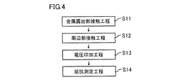
- FIG. 4 is a flowchart showing the insulation inspection method for the solar cell module of the present invention.
- the insulation test method for the solar cell module performed in the insulation inspection step S6 will be described below with reference to FIG.
- one of the pair of insulation inspection probes was brought into contact with the terminal block 107 in the terminal box 106.
- the metal exposed portion refers to a portion in the terminal box 106 including the terminal block 107 and the output lead wire 103 where the electromotive force generated by the photoelectric conversion element can be directly taken out.
- a connection portion between the power extraction cable 109 and the terminal block 107 is also included in the exposed metal portion.
- the other of the pair of insulation inspection probes was brought into contact with the frame of the solar cell module.
- the frame (peripheral part) of the solar cell module is made of aluminum.
- a voltage of 1000 V was applied between one insulation inspection probe and the other insulation inspection probe.
- the resistance value of the solar cell module was obtained by measuring the current flowing between one insulation inspection probe and the other insulation inspection probe.
- Example 2 When soldering is used as a joining means for electrically joining the output lead wire to the terminal block, the resin component or solder ball in the solder may scatter to the exposed metal portion.
- the contact resistance increased, and the insulation performance could not be measured continuously and accurately. It was found that one of the causes was that the scattered resin component in the solder formed a film on the exposed metal part, and the tip of the inspection probe did not fully contact the exposed metal part. In addition, when the scattered solder ball comes to the tip of the inspection probe, in the next inspection, the inspection probe comes into contact with the exposed metal portion through the solder attached to the inspection probe. I also found that there was something.
- This example solves the problem that occurs when the probe for insulation test of the above solar cell module is brought into contact with the exposed metal part in the terminal box.
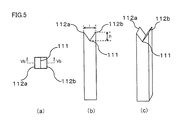
- FIG. 5 shows the tip of the insulation test probe of the solar cell module of Example 2.
- Fig.5 (a) is the figure which looked at the front-end
- FIG. 5B is a view showing a Vb-Vb cross section of FIG.
- FIG. 5C is a perspective view showing the tip of the probe.
- the tip of the probe has an M-shaped cross section, and a concave portion is formed from the opposed straight pointed portions 112a and 112b toward the center. The most depressed portion 111 in the center of the recess is linear.
- the height difference h between the most depressed portion 111 of the concave portion at the tip of the probe and the sharp portions 112a and 112b is 1.3 mm, and the probe is a rectangular parallelepiped having a side length i of 4 mm.
- the height difference h indicates the difference in height between the most depressed portion and the pointed portion of the probe tip.
- the length i of one side of the probe is desirably 2 mm or more. This is because the strength of the tip of the probe is stabilized.
- the pointed tip of the probe is a mountain and the most depressed portion is a valley.
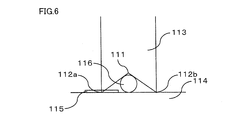
- FIG. 6 is a cross-sectional view showing a state in which an insulation inspection is performed using the insulation inspection probe of the solar cell module of this example.
- the solder ball When the output lead wire is connected to the terminal block by soldering, the solder ball may be scattered on the exposed metal part in the terminal box that contacts the probe.
- the tip portion 113 of the probe has a recess cut out in an M shape, and the height difference h is 1.3 mm, so that the solder ball 116 on the metal exposed portion 114 is Even when it enters the concave portion of the probe tip, the sharp portions 112a and 112b of the probe tip can come into contact with the metal exposed portion 114.
- the size of the solder balls scattered in the terminal box is not uniform, but the height difference between the most depressed part and the pointed part at the tip of the probe is sufficient if it is 1.3 mm. .
- the tip portion 113 of the probe is formed in an M shape, the solder ball 116 that has entered the recess does not remain at the tip of the probe. This is because the solder ball 116 escapes to the side without staying at the tip of the probe. Therefore, it becomes possible to use a probe continuously.
- the resin in the solder may remain on the surface of the exposed metal portion in the terminal box that contacts the probe.
- the pointed portions 112a and 112b at the tip of the probe even if the resin 115 in the solder is placed on the metal exposed portion 114, the tip portion of the probe breaks through the resin 115 in the solder, and the metal exposed portion 114 is exposed. It becomes possible to touch.
- the insulation inspection of the solar cell module including steps S11 to S14 shown in Example 1 was repeated 30 times with the solar cell module changed. After 30 times, the tip of the insulation test probe was checked. As a result, no solder balls remained in the recess at the tip of the probe. Since the concave portion at the tip of the probe penetrates to the end, it is presumed that even if there was a solder ball that entered the concave portion, it did not remain at the tip of the probe. As described above, by using the insulation test probe of this embodiment, continuous and accurate measurement can be performed without being affected by the scattering of solder balls generated during soldering.
- the insulation performance was not sufficient.
- the solar cell module with insufficient insulation performance it was not suitable for the subsequent step of attaching the lid of the terminal box.
- the contact of the insulation inspection probe with the exposed metal portion may be automatically performed using an apparatus.
- measurement failure may occur due to misalignment when the exposed metal part and the probe for insulation inspection are brought into contact with each other. desirable.
- Example 3 In FIG. 7, the front-end
- the difference between the third embodiment and the second embodiment is that the pointed portion of the probe tip is not a straight line but a dot.
- Fig.7 (a) is the figure which looked at the front-end
- FIG. 7B shows a VIIb-VIIb cross section of FIG. FIG.
- 7C is a perspective view of the tip of the probe.
- the entire probe has a rectangular parallelepiped shape, and the height difference between the pointed pointed portion and the most depressed portion is 1.3 mm, and the length of one side of the probe is 4 mm.
- the tip of the probe has an M-shaped cross section, and a concave portion is formed from the pointed pointed portions 112c and 112d facing each other toward the center.
- the most depressed portion 111 in the center of the recess is linear.
- the tip of the probe has the most depressed portion 111 of the concave portion constituted by a straight line and the sharpened portions 112c and 112d of the two probes.
- the tip of the probe has a recess, and the difference in height is 1.3 mm, so that the solder balls present on the exposed metal surface in the terminal box of the solar cell module have entered the recess. Even in this case, the solder ball is less likely to remain at the tip of the probe.
- the pointed tip of the probe is not a straight line but a dot, so even if there is resin in the solder on the exposed metal surface, the tip of the probe breaks through the resin more reliably. It becomes possible to contact the part.
- FIG. 8 is a diagram illustrating another example of the third embodiment. 8 differs from the example shown in FIG. 7 in that the shape of the entire probe is not a rectangular parallelepiped but a cylinder.
- FIG. 8A is a view of the tip of the probe viewed from directly above.
- FIG. 8B is a view showing a VIIIb-VIIIb cross section of FIG.
- FIG. 8C is a perspective view of the tip of the probe.
- the tip of the probe has an M-shaped cross section, and a concave portion is formed from the pointed pointed portions 112e and 112f facing each other toward the center.
- the most depressed portion 111 in the center of the recess is linear.
- FIG. 9 the tip of the probe for insulation inspection of the solar cell module of Example 4 is shown.
- the fourth embodiment is different from the third embodiment in that the shape of the entire probe is a cylinder, and there are four point-like pointed portions instead of two.
- FIG. 9A is a view of the tip of the probe as viewed from directly above.
- FIG. 9B is a view showing a IXb-IXb cross section of FIG.
- FIG. 9C is a front view of the tip of the probe.
- FIG. 9D is a side view of the tip of the probe.
- the entire probe has a cylindrical shape, and the height difference between the pointed pointed portion and the straightest most depressed portion is 1.3 mm, and the probe diameter is 4 mm.
- the tip of the probe has an M-shaped cross section, and the most depressed portion 111 at the center of the recess is linear.
- a recess is formed.
- the probe has a recess at the tip of the probe, and the height difference is 1.3 mm, so that the solder present on the exposed metal surface in the terminal box of the solar cell module Even when the ball enters the recess, the solder ball is less likely to remain at the tip of the probe.
- the pointed tip is not a straight line but a dot, even if there is solder resin on the exposed metal surface, the tip of the probe breaks through the resin more reliably and contacts the exposed metal part. It becomes possible.
- the number of pointed points is larger than in the case of two points, so it is possible to contact the exposed metal part more reliably.
- the contact area between the probe and the exposed metal portion increases, the contact resistance can be reduced.
- the cross-section of the probe tip is M-shaped, and there are two most recessed portions in the center of the linear recess, so the shape of the solder ball that enters the recess changes in four directions. It becomes possible to do. Therefore, even when the tip of the probe does not contact perpendicularly to the exposed metal surface, the solder ball is less likely to remain at the tip.
- FIG. 10 is a diagram illustrating another example of the fourth embodiment. Another example of the fourth embodiment is different from the example shown in FIG. 9 in that four point-like sharp portions are located inside the cylinder forming the probe. There are not only two recessed portions 111 but also four surrounding points.
- FIG. 10A is a view of the tip of the probe as viewed from directly above.
- FIG. 10B is a diagram showing a cross section taken along line Xb-Xb in FIG.
- FIG. 10C is a front view of the tip of the probe.
- the tip of the probe has an M-shaped cross section.
- the most depressed portion 111 of the recess is linear, and the most linearly depressed portion is two in the center and four on the outside. There are a total of six.
- Example 9 the height difference of the probe is 1.3 mm and the probe diameter is 4 mm, but the pointed point is inside the outer circumference of the cylinder, so that the probe is An area required for contact can be reduced. Therefore, it is possible to measure even when the area of the exposed metal portion is small.
- Example 5 In FIG. 11, the front-end
- FIG. 11A is a view of the tip of the probe as viewed from directly above.
- FIG. 11B is a view showing a XIb-XIb cross section of FIG.
- FIG. 11C is a front view of the tip of the probe.
- the tip of the probe has a shape in which a plurality of quadrangular pyramids are arranged, the most depressed portion 111 in the central portion of the recess is linear, and the five most depressed portions intersect each other. There are ten. There are 24 point-like pointed portions including pointed portions 112o, 112p, 112q, 112r, 112s, 112t, and 112u, which are located on the inside of the outer circumference of the cylinder at the tip of the probe.
- the probe of the embodiment shown using FIG. 11 has a cylindrical shape as a whole, the height difference is 0.5 mm, and the probe diameter is 4 mm. It was found that by increasing the number of the most depressed portions in the central part of the point-like pointed portion and the linear concave portion, the solder ball hardly remains at the tip even if the height difference is small.
- insulation inspection probe brought into contact with the peripheral inspection portion is not limited to the insulation inspection probes shown in the second to fifth embodiments.
- the solar cell module insulation inspection probe, solar cell module insulation inspection method, and solar cell module manufacturing method according to the present invention can be widely applied to the overall insulation inspection of solar cell modules.
Landscapes
- Physics & Mathematics (AREA)
- Geometry (AREA)
- General Physics & Mathematics (AREA)
- Photovoltaic Devices (AREA)
Abstract
本発明に係る太陽電池モジュールの絶縁検査用プローブは、絶縁検査用プローブの先端(113)に山(112)と谷(111)を有している。山(112)と谷(111)の高さの差は、0.5mm以上である。このような絶縁検査用プローブを用いることにより、太陽電池モジュールの光電変換素子と太陽電池モジュール周辺部との間の絶縁検査において、連続して正確な測定が可能となる。
Description
本発明は、太陽電池モジュールの絶縁検査用プローブ、検査用プローブを用いた太陽電池モジュールの絶縁検査方法、および太陽電池モジュールの製造方法に関する。
太陽電池は、半導体材料を利用した光電変換素子に太陽光等の光を入射させることによって、光電変換素子の正極と負極との間に起電力を生じさせるものである。また、太陽電池は、屋外に設置されることが多く、一般的に、光電変換素子を内部に封止した太陽電池モジュールとして設置される。
図12(a)および(b)に、特許文献1(特開2010-165749号公報)に開示された太陽電池モジュールの構造を示す。図12(a)は太陽電池モジュールの表面側を示し、図12(b)は太陽電池モジュールの裏面側を示す。図12(a)に示すように、太陽電池モジュール200は、直列に接続された多数の太陽電池セル201と、枠状のアルミニウム製の支持フレーム202からなっている。支持フレーム202は、透光性の高い前面カバー部材と、耐候性に優れた裏面カバー部材203と、その中間に封入する樹脂により太陽電池セル201を保護する構造体を支持するものである。図12(b)に示すように、端子ボックス装置205が、裏面カバー部材203に取り付けられ、太陽電池モジュール200の出力部を構成している。端子ボックス装置205には、他の太陽電池モジュール200に延びるモジュール連結ケーブル204が接続されている。
また、出力部を構成する部分の1つである端子ボックス装置の一般的な構造を以下に説明する。図13に、特許文献2(特開2001-168368号公報)に開示された太陽電池の出力部を構成する端子ボックスを示す。太陽電池用の端子ボックス装置205は、太陽電池の出力取出用電極材が挿通される挿通口209を有する筐体208の内部に、接続部210を備えた複数の中継端子207と、これらの中継端子207に接続されるバイパスダイオードとしての薄型ベアチップ206とを配設した太陽電池モジュールの出力部を構成するものである。太陽電池の出力取出用電極材として、太陽電池のプラス電極とマイナス電極にそれぞれ結線した二本のリード線が用いられている。この出力取出用電極材が、半田付等の接合手段によって接続部210に電気的に接続されている旨が特許文献2に開示されている。
太陽電池モジュールは、屋外で、雨に打たれるなどしても漏電が生じないよう、光電変換素子と周辺部材との間での絶縁性能が求められている。そのため、太陽電池モジュールの信頼性を確保するために、絶縁検査を行う必要がある。絶縁検査方法としては、たとえば、薄膜太陽電池モジュールの国際規格のひとつであるIEC61646、および結晶系太陽電池モジュールの国際規格のひとつであるIEC61215に、光電変換素子と太陽電池モジュールの周辺フレーム等の金属部分との間に電圧を印加し、絶縁試験を行う旨が規定されている。
図12で示した太陽電池モジュールにおいて、IEC61646およびIEC61215に規定された絶縁試験を行おうとすると、太陽電池セル201の出力部を構成する部分の1つであるモジュール連結ケーブル204と、アルミ製の支持フレーム202との間に電圧を印加し、絶縁試験を行うことになる。
しかしながら、太陽電池モジュールの連結ケーブルは、一般的に、先端はコネクタであり、電圧を印加する際にはプローブを差し込み、電圧印加後にはプローブをはずすという作業が必要となる。また、ケーブルは、柔軟性をもち動きやすいものであり、機械でつかむのは難しい。よって、太陽電池モジュールの連結ケーブルに、電圧を印加する工程の自動化が難しく、連続して正確に測定することが可能な、より簡易な検査方法が求められていた。
本発明は、上記の問題に鑑みてなされたものであり、その目的は、太陽電池モジュールの光電変換素子と太陽電池モジュール周辺部との間の絶縁検査において、連続して正確に測定することが可能となる、太陽電池モジュールの絶縁検査用プローブ、太陽電池モジュールの絶縁検査方法および太陽電池モジュールの製造方法を提供することにある。
本発明に係る太陽電池モジュールの絶縁検査用プローブは、先端に、山と谷を有しており、山と谷の高さの差は、0.5mm以上である。
本発明に係る太陽電池モジュールの絶縁検査用プローブにおいて好ましくは、上記谷は、半田ボールを逃がす機能を有している。
本発明に係る太陽電池モジュールの絶縁検査用プローブにおいて好ましくは、上記山の先端は直線状の形状を有している。
本発明に係る太陽電池モジュールの絶縁検査用プローブにおいて好ましくは、上記山の先端は点状の形状を有している。
本発明に係る太陽電池モジュールの絶縁検査用プローブにおいて好ましくは、上記谷は、複数個設けられている。
本発明に係る太陽電池モジュールの絶縁検査用プローブにおいて好ましくは、上記山と上記谷の高さの差は、1.3mm以上である。
本発明に係る太陽電池モジュールの絶縁検査方法は、太陽電池モジュールの一対の絶縁検査用プローブの一方を太陽電池モジュールの端子ボックス中の金属露出部に接触させる工程と、上記一対の絶縁検査用プローブの他方を、上記太陽電池モジュールの周辺部に接触させる工程と、上記絶縁検査用プローブの一方と上記絶縁検査用プローブの他方との間に電圧を印加する工程と、上記絶縁検査用プローブの一方と上記絶縁検査用プローブの他方との間の抵抗値を測定する工程とを有している。
本発明に係る太陽電池モジュールの絶縁検査方法において好ましくは、上記絶縁検査用プローブの先端が山と谷を有している。上記山と上記谷の高さの差は0.5mm以上である。
本発明に係る太陽電池モジュールの製造方法は、光電変換素子の電極端子部と電気的につながる出力リード線を端子ボックス中の端子台に固定する工程と、太陽電池モジュールの絶縁検査を行なう工程とを有している。上記太陽電池モジュールの絶縁検査を行なう工程は、太陽電池モジュールの一対の絶縁検査用プローブの一方を、太陽電池モジュールの端子ボックス中の金属露出部に接触させる工程と、絶縁検査用プローブの他方を、太陽電池モジュールの周辺部に接触させる工程と、上記絶縁検査用プローブの一方と上記絶縁検査用プローブの他方との間に電圧を印加する工程と、上記絶縁検査用プローブの一方と上記絶縁検査用プローブの他方との間の抵抗値を測定する工程とを有している。
本発明に係る太陽電池モジュールの絶縁検査用プローブ、太陽電池モジュールの絶縁検査方法および太陽電池モジュールの製造方法を用いることで、連続して正確に絶縁検査を行うことが可能となる。
(実施例1)
実施例1として、絶縁検査用プローブを用いた太陽電池モジュールの絶縁検査方法、および太陽電池モジュールの製造方法について説明する。
実施例1として、絶縁検査用プローブを用いた太陽電池モジュールの絶縁検査方法、および太陽電池モジュールの製造方法について説明する。
図1は、本発明の太陽電池モジュールの分解斜視図である。太陽電池モジュールは、基板上に形成された光電変換素子101の一端の表面電極上および他端部の裏面電極上に形成された端子電極を備えている。端子電極には、端子電極に重ねて配置されたバスバーリード102が接続されている。バスバーリード102は、半田めっきされた銅線で形成されている。また、バスバーリード102には、光電変換素子101で発生した電力を外部に取り出すための出力リード線103(特許文献2における出力取出用電極材)が、半田付けによって接続されている。出力リード線103は、絶縁部材であるPET(ポリエチレンテレフタレート)によって被覆された被覆導線を用いた。出力リード線103を設けた状態で、光電変換素子の裏面側を封止するために、裏面側に、充填部材シート104および裏面ガラス105が積層される。基板と裏面ガラス105は、真空ラミネート処理等の加熱加圧処理によって、充填部材シート104を介して接着される。充填部材シート104および裏面ガラス105は、いずれも出力リード線103の先端を引き出すための開口部を有している。
裏面ガラス105のリード引出し開口部から引き出された出力リード線103は、裏面ガラス105に接着固定される端子ボックス106内で、端子台(特許文献2における接続部)に接続され、同じく端子ボックス106内で端子台に接続された電力取り出しケーブル(特許文献2におけるモジュール連結ケーブル)を通じて外部に電力を取り出すことができる。
図2は、端子ボックスの蓋体を取り外した状態の平面図である。蓋体を取り外した端子ボックス106は、少なくとも、出力リード線103と、端子台107と、電力取り出しケーブル109を有している。また、太陽電池モジュールの裏面ガラス105の開口部から引き出された2本の出力リード線103を端子ボックス内部に導入するための2つのリード線開口部108を有している。リード線開口部108の横には、端子台107が設けられており、内部に導入された出力リード線103は、端子台107に固定されている。端子台107に固定された電力取り出しケーブル109により、端子ボックスから電力を取り出すことができる。
図3は、本発明の太陽電池モジュールの製造方法を示すフロー図である。図3を用いて、太陽電池モジュールの製造方法について以下に説明する。
まず、光電変換素子形成工程S1(Sはステップを表す。以下同様)において、光電変換素子を形成する。
その後、出力リード線取付け工程S2において、光電変換素子の両端に形成された端子電極にバスバーリード102を接続し、さらにバスバーリード102に出力リード線103を接続した。接続は、それぞれ半田付けによって行った。
その後、封止工程S3において、基板と、基板上に形成された光電変換素子101と、充填部材シート104と、裏面ガラス105を加熱封止した。
その後、端子ボックス取付け工程S4で、端子ボックス106を裏面ガラス105に接着固定した。
その後、出力リード線取付け工程S5で、出力リード線103を端子ボックス106中の端子台107に取付けた。取付け方法として、半田付けを用いた。
さらに、絶縁検査工程S6で、太陽電池モジュールの絶縁検査を行った。絶縁検査についての詳細は、後に、図4を用いて説明する。
さらに、端子ボックス蓋閉め工程S7で、端子ボックスの蓋を閉める。必要に応じて、端子ボックス内に充填材を入れる。充填材としては、絶縁性の樹脂が用いられる。充填材を入れることで、端子ボックス106の中に水がたまることを防ぐことが可能となる。
太陽電池モジュール製造工程の中で、簡易に絶縁試験を行うことができる段階を検討したところ、端子台に、出力リード線を接合した段階が、適当であることがわかった。この段階であれば、太陽電池モジュールの光電変換素子側として、端子台に検査用プローブを接触させ、絶縁試験のための電圧を印加することが可能である。この場合、連結ケーブルに検査用プローブをつないで電圧を印加するより、端子台に検査用プローブを接触させ電圧を印加する方が、より簡便に測定を行うことが可能であることがわかった。検査用プローブを上下させるという動作で済むためである。
図4は、本発明の太陽電池モジュールの絶縁検査方法を示すフロー図である。図4を用いて、絶縁検査工程S6で行う太陽電池モジュールの絶縁検査方法について以下に説明する。
まず、金属露出部接触工程S11において、端子ボックス106内の端子台107に、一対の絶縁検査用プローブの一方を接触させた。
なお、本明細書において、金属露出部とは、端子ボックス106内の、端子台107および出力リード線103を含む、光電変換素子で発生した起電力を直接取り出すことができる箇所を示す。電力取り出しケーブル109と端子台107との接続部も、金属露出部に含まれる。
次に、周辺部接触工程S12において、太陽電池モジュールのフレームに、一対の絶縁検査用プローブの他方を接触させた。太陽電池モジュールのフレーム(周辺部)は、アルミニウムで構成されている。
さらに、電圧印加工程S13において、一方の絶縁検査用プローブと他方の絶縁検査用プローブとの間に1000Vの電圧を印加した。
その後、抵抗測定工程S14において、一方の絶縁検査用プローブと他方の絶縁検査用プローブとの間に流れる電流を測定することで、太陽電池モジュールの抵抗値を得た。
絶縁検査工程S6で、絶縁性能が不十分と判断された太陽電池モジュールに関しては、続けて端子ボックス蓋閉め工程S7を行わないこととすることで、不要な作業工程を減らすことが可能となった。
(実施例2)
出力リード線を端子台に電気的に接合する際の接合手段として、半田付けを用いた場合、半田中の樹脂成分や半田ボールが、金属露出部に飛び散る場合があった。
(実施例2)
出力リード線を端子台に電気的に接合する際の接合手段として、半田付けを用いた場合、半田中の樹脂成分や半田ボールが、金属露出部に飛び散る場合があった。
一方、検査用プローブを金属露出部に接触させた場合、接触抵抗が大きくなり、連続して正確に絶縁性能を測定できないことがあった。その原因の1つとして、飛び散った半田中の樹脂成分が金属露出部に被膜を形成し、検査用プローブの先が金属露出部に十分に接触しない場合があるためであることがわかった。また、飛び散った半田ボールが、検査用プローブの先についた場合、次の検査では、検査用プローブは、先についた半田を介して金属露出部に接触することになるため、十分に接触しなくなることがあることもわかった。
本実施例は、上記の太陽電池モジュールの絶縁検査用プローブを端子ボックス内の金属露出部に接触させた場合におこる問題を解決するものである。
図5に、実施例2の太陽電池モジュールの絶縁検査用プローブの先端を示す。図5(a)は、プローブの先端を真上から見た図である。図5(b)は、図5(a)のVb-Vb断面を示す図である。図5(c)は、プローブの先端を示す斜視図である。プローブの先端は、断面がM字状に形成されており、対向する直線状の尖った部分112a,112bから中央に向かって凹部を形成している。凹部の中央部の一番窪んだ箇所111は、直線状になっている。プローブ先端の凹部の一番窪んだ箇所111と尖った部分112a,112bとの高さの差hは、1.3mmであり、プローブは一辺の長さiが4mmの直方体である。高さの差hとは、プローブ先端の一番窪んだ箇所と尖った部分との高さの差を示すものである。高さの差hが、1.3mmの場合、プローブの一辺の長さiは2mm以上が望ましい。プローブの先端の強度が安定するためである。
なお、本明細書において、プローブの先端の尖った部分を山とし、一番窪んだ箇所を谷とした。
図6は、本実施例の太陽電池モジュールの絶縁検査用プローブを用いて、絶縁検査を行う状態を示す断面図を示す。
プローブを接触させる端子ボックス中の金属露出部には、端子台に出力リード線を半田づけにより接続する際に、半田ボールが飛び散る場合がある。本実施例のように、プローブの先端部分113が、M字状に切り取られた凹部を有し、高さの差hが1.3mmあることで、金属露出部114上の半田ボール116が、プローブ先端の凹部に入りこんだ場合も、プローブ先端の尖った部分112a,112bは、金属露出部114に接触することが可能となる。端子ボックス中に飛び散った半田ボールの大きさは、一様ではないが、プローブ先端の一番窪んだ箇所と尖った部分との高さの差は、1.3mmあれば十分な大きさである。
また、プローブの先端部分113が、M字状に形成されていることで、凹部に入り込んだ半田ボール116は、プローブの先端に残らなくなる。なぜなら、半田ボール116は、プローブの先端に留まることなく、側方に逃げていくからである。よって、プローブを連続して用いることが可能となる。
さらに、プローブを接触させる端子ボックス中の金属露出部には、端子台に出力リード線を半田づけにより接続する際に、半田中の樹脂が表面に残る場合がある。プローブの先端に尖った部分112a,112bを有することで、金属露出部114上に半田中の樹脂115が載っている場合でも、プローブの先端部分は半田中の樹脂115を突き破り、金属露出部114に接触することが可能となる。
本実施例の検査プローブを用いて、実施例1で示した工程S11~S14を含む太陽電池モジュールの絶縁検査を、太陽電池モジュールを変え、繰り返し30回行った。30回行った後で、絶縁試験用プローブの先端を確認したところ、プローブの先端部分にある凹部への半田ボールの残留は観察されなかった。プローブの先端部分にある凹部が端まで貫通していることで、凹部に入り込んだ半田ボールがあった場合でも、プローブの先端には残留しなかったと推測される。以上のように、本実施例の絶縁検査用プローブを用いたことで、半田づけの際に発生する半田ボールの飛び散りの影響を受けず、連続した正確な測定が可能となった。
また、絶縁検査を30回行った中で、絶縁性能が十分ではないものがあった。絶縁性能が不十分な太陽電池モジュールに関しては、この後の端子ボックスの蓋体を取り付ける工程にはまわさなかった。端子ボックスの蓋体を取り付ける前に絶縁検査を行ったことで、早い段階で不良品を見つけることができ、その後の工程を行わないことが可能となった。
金属露出部への絶縁検査用プローブの接触は、装置を用いて自動で行ってもよい。自動で行う場合には、金属露出部と絶縁検査用プローブを接触させる際の位置ずれによる、測定不良が発生する可能性があるため、絶縁端子用プローブの先端部分の接触する面積は小さい方が望ましい。測定を安定させるためには、金属露出部の面積の1/2以下とすることが適当である。
(実施例3)
図7に、実施例3の太陽電池モジュールの絶縁検査用プローブの先端を示す。実施例3が実施例2と異なる点は、プローブの先端の尖った部分が直線状ではなく点状であることである。図7(a)は、プローブの先端を真上から見た図である。図7(b)は、図7(a)のVIIb-VIIb断面を示すものである。図7(c)は、プローブの先端の斜視図である。プローブ全体は直方体の形状を持っており、点状の尖った部分と、一番窪んだ箇所の高さの差は1.3mm、プローブの一辺の長さは4mmである。プローブの先端は、断面がM字状に形成されており、向いあう点状の尖った部分112c,112dから中央に向かって凹部を形成している。凹部の中央部の一番窪んだ箇所111は、直線状になっている。
(実施例3)
図7に、実施例3の太陽電池モジュールの絶縁検査用プローブの先端を示す。実施例3が実施例2と異なる点は、プローブの先端の尖った部分が直線状ではなく点状であることである。図7(a)は、プローブの先端を真上から見た図である。図7(b)は、図7(a)のVIIb-VIIb断面を示すものである。図7(c)は、プローブの先端の斜視図である。プローブ全体は直方体の形状を持っており、点状の尖った部分と、一番窪んだ箇所の高さの差は1.3mm、プローブの一辺の長さは4mmである。プローブの先端は、断面がM字状に形成されており、向いあう点状の尖った部分112c,112dから中央に向かって凹部を形成している。凹部の中央部の一番窪んだ箇所111は、直線状になっている。
図7(a)で示したように、プローブの先端は、直線で構成される凹部の一番窪んだ箇所111と、2つのプローブの先端の尖った部分112c,112dを有する。
実施例2と同様に、プローブの先端部分が凹部を有し、高さの差が1.3mmあることで、太陽電池モジュールの端子ボックス中の金属露出面に存在する半田ボールが凹部に入り込んだ場合も、半田ボールが、プローブの先端に残りにくくなる。さらに、プローブ先端の尖った箇所が、直線状ではなく点状であることで、金属露出面上に半田中の樹脂があった場合でも、より確実にプローブの先端部分が樹脂を突き破り、金属露出部に接触することが可能となる。
図8は、実施例3の別の例を示す図である。図8の別の例が図7で示した例と異なる点は、プローブ全体の形状が直方体ではなく、円柱であることである。図8(a)は、プローブの先端を真上から見た図である。図8(b)は、図8(a)のVIIIb-VIIIb断面を示す図である。図8(c)は、プローブの先端の斜視図である。プローブの先端は、断面がM字状に形成されており、向いあう点状の尖った部分112e,112fから中央に向かって凹部を形成している。凹部の中央部の一番窪んだ箇所111は、直線状になっている。プローブ全体の形状は、円柱であっても、直方体の場合と同様の効果を得ることができる。
(実施例4)
図9に、実施例4の太陽電池モジュールの絶縁検査用プローブの先端を示す。実施例4が実施例3と異なる点は、プローブ全体の形状が円柱であり、さらに、プローブの先端の点状の尖った部分が2個ではなく、4個ある点である。図9(a)は、プローブの先端を真上から見た図である。図9(b)は、図9(a)のIXb-IXb断面を示す図である。図9(c)は、プローブの先端の正面図である。図9(d)は、プローブの先端の側面図である。プローブ全体は円柱体の形状を持っており、点状の尖った部分と直線状の一番窪んだ箇所の高さの差は1.3mm、プローブの直径は4mmである。
(実施例4)
図9に、実施例4の太陽電池モジュールの絶縁検査用プローブの先端を示す。実施例4が実施例3と異なる点は、プローブ全体の形状が円柱であり、さらに、プローブの先端の点状の尖った部分が2個ではなく、4個ある点である。図9(a)は、プローブの先端を真上から見た図である。図9(b)は、図9(a)のIXb-IXb断面を示す図である。図9(c)は、プローブの先端の正面図である。図9(d)は、プローブの先端の側面図である。プローブ全体は円柱体の形状を持っており、点状の尖った部分と直線状の一番窪んだ箇所の高さの差は1.3mm、プローブの直径は4mmである。
プローブの先端は、断面がM字状に形成されており、凹部の中央部の一番窪んだ箇所111は直線状になっている。本実施例において、直線状の一番窪んだ箇所は2本、向いあう点状の尖った部分は2組あり、尖った部分112g,112iと、尖った部分112h,112jとはそれぞれ中央に向かって、凹部を形成している。
実施例2および実施例3と同様に、プローブの先端部分に、凹部を有し、高さの差が1.3mmあることで、太陽電池モジュールの端子ボックス中の金属露出面上に存在する半田ボールが凹部に入り込んだ場合も、半田ボールがプローブの先端に残りにくくなる。かつ、先端の尖った箇所が直線状でなく点状であることで、金属露出面上に半田の樹脂があった場合でも、より確実にプローブの先端が樹脂を突き破り、金属露出部に接触することが可能となる。
さらに、プローブの先端に、点状の4個の尖った箇所を有することで、尖った箇所が2個の場合と比較して数が多いため、より確実に金属露出部に接触することが可能となるとともに、プローブと金属露出部の接触面積が増えるため、接触抵抗を小さくすることが可能となる。
さらに、プローブ先端の断面がM字状に形成されており、直線状の凹部の中央部の一番窪んだ箇所が2本あることで、凹部に入り込んだ半田ボールの形状は、4方向に変化することが可能となる。よって、プローブの先端が、金属露出面に対し垂直に接触しなかった場合でも、半田ボールが先端に残りにくくなる。
なお、2本の直線状の一番窪んだ箇所は、互いに垂直に交わる必要はない。
図10は、実施例4の別の例を示す図である。実施例4の別の例が図9で示した例と異なる点は、4個の点状の尖った部分がプローブを形成する円柱の内側に位置しているため、直線状の凹部の一番窪んだ箇所111が、2本だけではなく、さらに周囲に4本ある点である。
図10は、実施例4の別の例を示す図である。実施例4の別の例が図9で示した例と異なる点は、4個の点状の尖った部分がプローブを形成する円柱の内側に位置しているため、直線状の凹部の一番窪んだ箇所111が、2本だけではなく、さらに周囲に4本ある点である。
図10(a)は、プローブの先端を真上から見た図である。図10(b)は、図10(a)のXb-Xb断面を示す図である。図10(c)は、プローブの先端の正面図である。プローブの先端は、断面がM字状に形成されており、凹部の一番窪んだ箇所111は直線状になっており、直線状の一番窪んだ箇所は中央に2本、外側に4本の計6本ある。向いあう点状の尖った部分は、尖った部分112k,112mと、尖った部分112l,112nの4個あり、プローブの先端の円柱の外周より内側にある。図9で示した例と同じく、プローブの高さの差は1.3mm、プローブの直径は4mmであるが、点状の尖った部分が、円柱の外周円の内側にあることで、プローブが接触するために必要な面積を小さくすることができる。よって、金属露出部の面積が小さい場合にも測定することが可能となる。
(実施例5)
図11に、実施例5の太陽電池モジュールの絶縁検査用プローブの先端を示す。実施例4で示した例と異なる点は、点状の尖った部分が24個あり、直線状の凹部の一番窪んだ箇所111は、2本ではなく10本ある点と、プローブの高さの差である。
(実施例5)
図11に、実施例5の太陽電池モジュールの絶縁検査用プローブの先端を示す。実施例4で示した例と異なる点は、点状の尖った部分が24個あり、直線状の凹部の一番窪んだ箇所111は、2本ではなく10本ある点と、プローブの高さの差である。
図11(a)は、プローブの先端を真上から見た図である。図11(b)は、図11(a)のXIb-XIb断面を示す図である。図11(c)は、プローブの先端の正面図である。プローブの先端は、四角錐が複数並んだ形をしており、凹部の中央部の一番窪んだ箇所111は直線状になっており、直線状の一番窪んだ箇所は5本づつ交差して10本ある。点状の尖った部分は、尖った部分112o,112p,112q,112r,112s,112t,112uを含み24個あり、プローブの先端の円柱の外周上の内側にある。
図11を用いて示したように、プローブの先端に、点状の尖った部分の数を多くすることで、より確実に金属露出部に接触することが可能となるとともに、プローブと金属露出部の接触面積が増えるため、接触抵抗を小さくすることが可能となる。
さらに、点状の尖った部分と直線状の凹部の一番窪んだ箇所の数を多くしたことで、プローブの先端が、金属露出面に対し垂直に接触しなかった場合でも、半田ボールは、より先端に残りにくくなる。
図11を用いて示した実施例のプローブは、プローブ全体は円柱体の形状を持っており、高さの差は0.5mm、プローブの直径は4mmである。点状の尖った部分と直線状の凹部の中央部の一番窪んだ箇所の数を多くしたことで、高さの差が小さくても、半田ボールが先端に残りにくくなることがわかった。
なお、周辺検査部に接触させる絶縁検査用プローブは、実施例2から5で示した絶縁検査用プローブに限定されるものではない。
以上、本発明の実施の形態について説明したが、今回開示された実施の形態はすべての点で例示であって制限的なものではないと考えられるべきである。本発明の範囲は請求の範囲によって示され、請求の範囲と均等の意味および範囲内でのすべての変更が含まれることが意図される。
本発明に係る太陽電池モジュールの絶縁検査用プローブ、太陽電池モジュールの絶縁検査方法および太陽電池モジュールの製造方法は、太陽電池モジュールの絶縁検査全般に広く適用することができる。
101 光電変換素子、102 バスバーリード、103 出力リード線、104 充填部材シート、105 裏面ガラス、106 端子ボックス、107 端子台、108 リード線開口部、109 電力取り出しケーブル、111 一番窪んだ箇所(谷)、112 尖った部分(山)、113 プローブの先端部分、114 金属露出部、115 半田中の樹脂、116 半田ボール。
Claims (9)
- 太陽電池モジュールの絶縁検査用プローブであって、
前記絶縁検査用プローブの先端(113)は、山(112)と谷(111)を有しており、
前記山(112)と前記谷(111)の高さの差は、0.5mm以上である、太陽電池モジュールの絶縁検査用プローブ。 - 前記谷(111)は、半田ボールを逃がす機能を有する、請求項1記載の太陽電池モジュールの絶縁検査用プローブ。
- 前記山(112)の先端は直線状の形状を有する、請求項1または2記載の太陽電池モジュールの絶縁検査用プローブ。
- 前記山(112)の先端は点状の形状を有する、請求項1または2記載の太陽電池モジュールの絶縁検査用プローブ。
- 前記谷(111)は複数個設けられている、請求項1から4のいずれかに記載の太陽電池モジュールの絶縁検査用プローブ。
- 前記山(112)と前記谷(111)の高さの差は、1.3mm以上である、請求項1から5のいずれかに1記載の太陽電池モジュールの絶縁検査用プローブ。
- 太陽電池モジュールの絶縁検査方法であって、
一対の絶縁検査用プローブの一方を、前記太陽電池モジュールの端子ボックス(106)中の金属露出部(114)に接触させる工程と、
前記一対の絶縁検査用プローブの他方を、前記太陽電池モジュールの周辺部に接触させる工程と、
前記絶縁検査用プローブの一方と前記絶縁検査用プローブの他方との間に電圧を印加する工程と、
前記絶縁検査用プローブの一方と前記絶縁検査用プローブの他方との間の抵抗値を測定する工程とを有する、太陽電池モジュールの絶縁検査方法。 - 前記絶縁検査用プローブは、先端が山(112)と谷(111)を有し、前記山(112)と前記谷(111)の高さの差が0.5mm以上である、請求項7記載の太陽電池モジュールの絶縁検査方法。
- 光電変換素子(101)の電極端子部と電気的につながる出力リード線(103)を端子ボックス(106)中の端子台(107)に固定する工程と、太陽電池モジュールの絶縁検査を行なう工程とを有する太陽電池モジュールの製造方法であって、
前記太陽電池モジュールの絶縁検査を行なう工程は、
太陽電池モジュールの一対の絶縁検査用プローブの一方を、太陽電池モジュールの端子ボックス(106)中の金属露出部(114)に接触させる工程と、
前記一対の絶縁検査用プローブの他方を、太陽電池モジュールの周辺部に接触させる工程と、
前記絶縁検査用プローブの一方と前記絶縁検査用プローブの他方との間に電圧を印加する工程と、
前記絶縁検査用プローブの一方と前記絶縁検査用プローブの他方との間の抵抗値を測定する工程とを有する、太陽電池モジュールの製造方法。
Applications Claiming Priority (2)
| Application Number | Priority Date | Filing Date | Title |
|---|---|---|---|
| JP2011-257001 | 2011-11-25 | ||
| JP2011257001A JP2015035435A (ja) | 2011-11-25 | 2011-11-25 | 太陽電池モジュールの絶縁検査用プローブ、検査用プローブを用いた太陽電池モジュールの絶縁検査方法、および太陽電池モジュールの製造方法。 |
Publications (1)
| Publication Number | Publication Date |
|---|---|
| WO2013077057A1 true WO2013077057A1 (ja) | 2013-05-30 |
Family
ID=48469516
Family Applications (1)
| Application Number | Title | Priority Date | Filing Date |
|---|---|---|---|
| PCT/JP2012/072583 Ceased WO2013077057A1 (ja) | 2011-11-25 | 2012-09-05 | 太陽電池モジュールの絶縁検査用プローブ、太陽電池モジュールの絶縁検査方法、および太陽電池モジュールの製造方法 |
Country Status (2)
| Country | Link |
|---|---|
| JP (1) | JP2015035435A (ja) |
| WO (1) | WO2013077057A1 (ja) |
Cited By (1)
| Publication number | Priority date | Publication date | Assignee | Title |
|---|---|---|---|---|
| CN105706359A (zh) * | 2013-11-08 | 2016-06-22 | 迪睿合株式会社 | 太阳能电池单体用输出测定夹具及太阳能电池单体的输出测定方法 |
Citations (4)
| Publication number | Priority date | Publication date | Assignee | Title |
|---|---|---|---|---|
| JPH0460462A (ja) * | 1990-06-29 | 1992-02-26 | Fujitsu Ltd | 電気的接触子 |
| JP2009503535A (ja) * | 2005-08-03 | 2009-01-29 | パイコム コーポレーション | 垂直型プローブ、その製造方法及びプローブのボンディング方法 |
| JP2010177379A (ja) * | 2009-01-28 | 2010-08-12 | Mitsubishi Electric Corp | 太陽電池用測定治具 |
| JP2011080901A (ja) * | 2009-10-08 | 2011-04-21 | Renesas Electronics Corp | プローブ、icソケット、試験装置、および、試験方法 |
-
2011
- 2011-11-25 JP JP2011257001A patent/JP2015035435A/ja active Pending
-
2012
- 2012-09-05 WO PCT/JP2012/072583 patent/WO2013077057A1/ja not_active Ceased
Patent Citations (4)
| Publication number | Priority date | Publication date | Assignee | Title |
|---|---|---|---|---|
| JPH0460462A (ja) * | 1990-06-29 | 1992-02-26 | Fujitsu Ltd | 電気的接触子 |
| JP2009503535A (ja) * | 2005-08-03 | 2009-01-29 | パイコム コーポレーション | 垂直型プローブ、その製造方法及びプローブのボンディング方法 |
| JP2010177379A (ja) * | 2009-01-28 | 2010-08-12 | Mitsubishi Electric Corp | 太陽電池用測定治具 |
| JP2011080901A (ja) * | 2009-10-08 | 2011-04-21 | Renesas Electronics Corp | プローブ、icソケット、試験装置、および、試験方法 |
Cited By (2)
| Publication number | Priority date | Publication date | Assignee | Title |
|---|---|---|---|---|
| CN105706359A (zh) * | 2013-11-08 | 2016-06-22 | 迪睿合株式会社 | 太阳能电池单体用输出测定夹具及太阳能电池单体的输出测定方法 |
| CN105706359B (zh) * | 2013-11-08 | 2018-05-29 | 迪睿合株式会社 | 太阳能电池单体用输出测定夹具及太阳能电池单体的输出测定方法 |
Also Published As
| Publication number | Publication date |
|---|---|
| JP2015035435A (ja) | 2015-02-19 |
Similar Documents
| Publication | Publication Date | Title |
|---|---|---|
| JP5144582B2 (ja) | 蓄電装置の漏液伝達抑制構造 | |
| TWI574020B (zh) | Method for measuring the output of a solar cell and a method for measuring the output of a solar cell | |
| KR101106109B1 (ko) | 전지셀 어셈블리들의 상호연결 장치 | |
| US20120100731A1 (en) | Connection terminal, terminal connection structure, and terminal box | |
| JP2019501540A (ja) | 光起電力ストリング及びモジュール用の相互接続方法 | |
| CN102044653A (zh) | 连接装置 | |
| JP2011519170A (ja) | 太陽電池の接触を形成する方法 | |
| CN107810566A (zh) | 用于电池模块的盖组件 | |
| CN103063855A (zh) | 一种用于宇航用叠层封装器件的破坏性物理分析方法 | |
| KR200455080Y1 (ko) | 태양전지 검사용 프로브 유닛 | |
| JP2014022702A (ja) | 太陽電池モジュール用ジャンクションボックス及び太陽電池モジュールの製造方法 | |
| CN105336813A (zh) | 太阳能电池组件的制作方法 | |
| WO2013077057A1 (ja) | 太陽電池モジュールの絶縁検査用プローブ、太陽電池モジュールの絶縁検査方法、および太陽電池モジュールの製造方法 | |
| CN105425138B (zh) | 失效分析系统 | |
| CN104134872B (zh) | 带电池监测器模块和连到其分流器的电缆的电池监测组件 | |
| KR101400733B1 (ko) | 도전 부재의 표면 구조 및 그 표면 구조를 구비한 와셔, 압착 단자 | |
| TWI595696B (zh) | Battery connection module | |
| JP2013213795A (ja) | 測定治具 | |
| KR101089090B1 (ko) | 전지의 절연저항 측정용 고정장치 | |
| CN220914521U (zh) | 动力电池 | |
| JP2011151188A (ja) | 太陽電池モジュール用端子ボックス、それを用いた太陽電池モジュール、及びその製造方法 | |
| JP2013131668A (ja) | 測定治具 | |
| Rendler et al. | Wave-shaped wires soldered on the finger grid of solar cells: Solder joint stability under thermal cycling | |
| CN203086837U (zh) | 带有引线的电路板及带有引线的电池组 | |
| CN112310564A (zh) | 一种电池用集成模块加工方法 |
Legal Events
| Date | Code | Title | Description |
|---|---|---|---|
| 121 | Ep: the epo has been informed by wipo that ep was designated in this application |
Ref document number: 12851578 Country of ref document: EP Kind code of ref document: A1 |
|
| NENP | Non-entry into the national phase |
Ref country code: DE |
|
| 122 | Ep: pct application non-entry in european phase |
Ref document number: 12851578 Country of ref document: EP Kind code of ref document: A1 |
|
| NENP | Non-entry into the national phase |
Ref country code: JP |