WO2013069878A1 - Optical sheet, display device and light emitting device having the same - Google Patents
Optical sheet, display device and light emitting device having the same Download PDFInfo
- Publication number
- WO2013069878A1 WO2013069878A1 PCT/KR2012/006308 KR2012006308W WO2013069878A1 WO 2013069878 A1 WO2013069878 A1 WO 2013069878A1 KR 2012006308 W KR2012006308 W KR 2012006308W WO 2013069878 A1 WO2013069878 A1 WO 2013069878A1
- Authority
- WO
- WIPO (PCT)
- Prior art keywords
- light
- layer
- conversion
- optical member
- light conversion
- Prior art date
Links
- 230000003287 optical effect Effects 0.000 title claims abstract description 40
- 238000006243 chemical reaction Methods 0.000 claims abstract description 215
- 239000002245 particle Substances 0.000 claims abstract description 99
- 238000009792 diffusion process Methods 0.000 claims abstract description 38
- 239000011347 resin Substances 0.000 claims description 8
- 229920005989 resin Polymers 0.000 claims description 8
- VYPSYNLAJGMNEJ-UHFFFAOYSA-N Silicium dioxide Chemical compound O=[Si]=O VYPSYNLAJGMNEJ-UHFFFAOYSA-N 0.000 claims description 6
- 239000011324 bead Substances 0.000 claims description 6
- 229920001490 poly(butyl methacrylate) polymer Polymers 0.000 claims description 4
- 229920003229 poly(methyl methacrylate) Polymers 0.000 claims description 4
- 239000004926 polymethyl methacrylate Substances 0.000 claims description 4
- 239000004793 Polystyrene Substances 0.000 claims description 2
- GWEVSGVZZGPLCZ-UHFFFAOYSA-N Titan oxide Chemical compound O=[Ti]=O GWEVSGVZZGPLCZ-UHFFFAOYSA-N 0.000 claims description 2
- 229910001593 boehmite Inorganic materials 0.000 claims description 2
- FAHBNUUHRFUEAI-UHFFFAOYSA-M hydroxidooxidoaluminium Chemical compound O[Al]=O FAHBNUUHRFUEAI-UHFFFAOYSA-M 0.000 claims description 2
- TWNQGVIAIRXVLR-UHFFFAOYSA-N oxo(oxoalumanyloxy)alumane Chemical compound O=[Al]O[Al]=O TWNQGVIAIRXVLR-UHFFFAOYSA-N 0.000 claims description 2
- BPUBBGLMJRNUCC-UHFFFAOYSA-N oxygen(2-);tantalum(5+) Chemical compound [O-2].[O-2].[O-2].[O-2].[O-2].[Ta+5].[Ta+5] BPUBBGLMJRNUCC-UHFFFAOYSA-N 0.000 claims description 2
- 229920002223 polystyrene Polymers 0.000 claims description 2
- 239000000377 silicon dioxide Substances 0.000 claims description 2
- 229910052814 silicon oxide Inorganic materials 0.000 claims description 2
- 229910001936 tantalum oxide Inorganic materials 0.000 claims description 2
- OGIDPMRJRNCKJF-UHFFFAOYSA-N titanium oxide Inorganic materials [Ti]=O OGIDPMRJRNCKJF-UHFFFAOYSA-N 0.000 claims description 2
- 239000010410 layer Substances 0.000 description 176
- 239000000758 substrate Substances 0.000 description 67
- 239000004973 liquid crystal related substance Substances 0.000 description 27
- 239000002096 quantum dot Substances 0.000 description 26
- 239000004065 semiconductor Substances 0.000 description 26
- 239000002159 nanocrystal Substances 0.000 description 12
- 239000000463 material Substances 0.000 description 10
- 238000005286 illumination Methods 0.000 description 9
- 239000010409 thin film Substances 0.000 description 6
- 239000013110 organic ligand Substances 0.000 description 5
- 229920000642 polymer Polymers 0.000 description 5
- 150000001875 compounds Chemical class 0.000 description 4
- 239000011342 resin composition Substances 0.000 description 4
- 239000000126 substance Substances 0.000 description 4
- QVGXLLKOCUKJST-UHFFFAOYSA-N atomic oxygen Chemical compound [O] QVGXLLKOCUKJST-UHFFFAOYSA-N 0.000 description 3
- 239000011247 coating layer Substances 0.000 description 3
- 229910052751 metal Inorganic materials 0.000 description 3
- 239000002184 metal Substances 0.000 description 3
- 238000012986 modification Methods 0.000 description 3
- 230000004048 modification Effects 0.000 description 3
- 229910052760 oxygen Inorganic materials 0.000 description 3
- 239000001301 oxygen Substances 0.000 description 3
- 239000000049 pigment Substances 0.000 description 3
- 229920000139 polyethylene terephthalate Polymers 0.000 description 3
- 239000005020 polyethylene terephthalate Substances 0.000 description 3
- 229910052709 silver Inorganic materials 0.000 description 3
- XBBZAULFUPBZSP-UHFFFAOYSA-N 2,4-dichloro-1-(3-chlorophenyl)benzene Chemical compound ClC1=CC(Cl)=CC=C1C1=CC=CC(Cl)=C1 XBBZAULFUPBZSP-UHFFFAOYSA-N 0.000 description 2
- 229910004613 CdTe Inorganic materials 0.000 description 2
- 229910004262 HgTe Inorganic materials 0.000 description 2
- 229920000106 Liquid crystal polymer Polymers 0.000 description 2
- 239000004977 Liquid-crystal polymers (LCPs) Substances 0.000 description 2
- XYFCBTPGUUZFHI-UHFFFAOYSA-N Phosphine Chemical compound P XYFCBTPGUUZFHI-UHFFFAOYSA-N 0.000 description 2
- JUJWROOIHBZHMG-UHFFFAOYSA-N Pyridine Chemical compound C1=CC=NC=C1 JUJWROOIHBZHMG-UHFFFAOYSA-N 0.000 description 2
- XUIMIQQOPSSXEZ-UHFFFAOYSA-N Silicon Chemical compound [Si] XUIMIQQOPSSXEZ-UHFFFAOYSA-N 0.000 description 2
- 229910007709 ZnTe Inorganic materials 0.000 description 2
- 229910052782 aluminium Inorganic materials 0.000 description 2
- 230000004888 barrier function Effects 0.000 description 2
- UHYPYGJEEGLRJD-UHFFFAOYSA-N cadmium(2+);selenium(2-) Chemical compound [Se-2].[Cd+2] UHYPYGJEEGLRJD-UHFFFAOYSA-N 0.000 description 2
- 229910052956 cinnabar Inorganic materials 0.000 description 2
- 239000003086 colorant Substances 0.000 description 2
- 230000000694 effects Effects 0.000 description 2
- 239000011159 matrix material Substances 0.000 description 2
- 230000035515 penetration Effects 0.000 description 2
- 230000035699 permeability Effects 0.000 description 2
- SBIBMFFZSBJNJF-UHFFFAOYSA-N selenium;zinc Chemical compound [Se]=[Zn] SBIBMFFZSBJNJF-UHFFFAOYSA-N 0.000 description 2
- 239000010703 silicon Substances 0.000 description 2
- 229910052710 silicon Inorganic materials 0.000 description 2
- 239000002904 solvent Substances 0.000 description 2
- 229910052950 sphalerite Inorganic materials 0.000 description 2
- 229910052984 zinc sulfide Inorganic materials 0.000 description 2
- 229910002704 AlGaN Inorganic materials 0.000 description 1
- 229910016423 CuZnS Inorganic materials 0.000 description 1
- 239000004593 Epoxy Substances 0.000 description 1
- LFQSCWFLJHTTHZ-UHFFFAOYSA-N Ethanol Chemical compound CCO LFQSCWFLJHTTHZ-UHFFFAOYSA-N 0.000 description 1
- BQCADISMDOOEFD-UHFFFAOYSA-N Silver Chemical compound [Ag] BQCADISMDOOEFD-UHFFFAOYSA-N 0.000 description 1
- 230000008033 biological extinction Effects 0.000 description 1
- 230000015572 biosynthetic process Effects 0.000 description 1
- 239000000919 ceramic Substances 0.000 description 1
- 229910010293 ceramic material Inorganic materials 0.000 description 1
- 239000004020 conductor Substances 0.000 description 1
- 238000005520 cutting process Methods 0.000 description 1
- 230000005611 electricity Effects 0.000 description 1
- 230000002708 enhancing effect Effects 0.000 description 1
- 239000003822 epoxy resin Substances 0.000 description 1
- 238000005530 etching Methods 0.000 description 1
- 239000010408 film Substances 0.000 description 1
- 230000017525 heat dissipation Effects 0.000 description 1
- 238000002347 injection Methods 0.000 description 1
- 239000007924 injection Substances 0.000 description 1
- 238000001746 injection moulding Methods 0.000 description 1
- 238000010030 laminating Methods 0.000 description 1
- 239000007769 metal material Substances 0.000 description 1
- 238000000034 method Methods 0.000 description 1
- 239000002078 nanoshell Substances 0.000 description 1
- 239000003960 organic solvent Substances 0.000 description 1
- AUONHKJOIZSQGR-UHFFFAOYSA-N oxophosphane Chemical compound P=O AUONHKJOIZSQGR-UHFFFAOYSA-N 0.000 description 1
- 238000000059 patterning Methods 0.000 description 1
- 230000002093 peripheral effect Effects 0.000 description 1
- 229910000073 phosphorus hydride Inorganic materials 0.000 description 1
- 229920000647 polyepoxide Polymers 0.000 description 1
- 229920001955 polyphenylene ether Polymers 0.000 description 1
- 239000002243 precursor Substances 0.000 description 1
- 239000011241 protective layer Substances 0.000 description 1
- 238000004080 punching Methods 0.000 description 1
- UMJSCPRVCHMLSP-UHFFFAOYSA-N pyridine Natural products COC1=CC=CN=C1 UMJSCPRVCHMLSP-UHFFFAOYSA-N 0.000 description 1
- 238000006862 quantum yield reaction Methods 0.000 description 1
- 238000009877 rendering Methods 0.000 description 1
- 238000007789 sealing Methods 0.000 description 1
- 239000002210 silicon-based material Substances 0.000 description 1
- 239000004332 silver Substances 0.000 description 1
- 229910000679 solder Inorganic materials 0.000 description 1
- 239000000243 solution Substances 0.000 description 1
- 230000000087 stabilizing effect Effects 0.000 description 1
- PXQLVRUNWNTZOS-UHFFFAOYSA-N sulfanyl Chemical class [SH] PXQLVRUNWNTZOS-UHFFFAOYSA-N 0.000 description 1
- 238000003786 synthesis reaction Methods 0.000 description 1
- 125000003396 thiol group Chemical class [H]S* 0.000 description 1
- 238000002834 transmittance Methods 0.000 description 1
Images


Classifications
-
- G—PHYSICS
- G02—OPTICS
- G02F—OPTICAL DEVICES OR ARRANGEMENTS FOR THE CONTROL OF LIGHT BY MODIFICATION OF THE OPTICAL PROPERTIES OF THE MEDIA OF THE ELEMENTS INVOLVED THEREIN; NON-LINEAR OPTICS; FREQUENCY-CHANGING OF LIGHT; OPTICAL LOGIC ELEMENTS; OPTICAL ANALOGUE/DIGITAL CONVERTERS
- G02F1/00—Devices or arrangements for the control of the intensity, colour, phase, polarisation or direction of light arriving from an independent light source, e.g. switching, gating or modulating; Non-linear optics
- G02F1/01—Devices or arrangements for the control of the intensity, colour, phase, polarisation or direction of light arriving from an independent light source, e.g. switching, gating or modulating; Non-linear optics for the control of the intensity, phase, polarisation or colour
- G02F1/13—Devices or arrangements for the control of the intensity, colour, phase, polarisation or direction of light arriving from an independent light source, e.g. switching, gating or modulating; Non-linear optics for the control of the intensity, phase, polarisation or colour based on liquid crystals, e.g. single liquid crystal display cells
- G02F1/133—Constructional arrangements; Operation of liquid crystal cells; Circuit arrangements
- G02F1/1333—Constructional arrangements; Manufacturing methods
- G02F1/1335—Structural association of cells with optical devices, e.g. polarisers or reflectors
- G02F1/1336—Illuminating devices
- G02F1/133617—Illumination with ultraviolet light; Luminescent elements or materials associated to the cell
-
- G—PHYSICS
- G02—OPTICS
- G02B—OPTICAL ELEMENTS, SYSTEMS OR APPARATUS
- G02B6/00—Light guides; Structural details of arrangements comprising light guides and other optical elements, e.g. couplings
- G02B6/0001—Light guides; Structural details of arrangements comprising light guides and other optical elements, e.g. couplings specially adapted for lighting devices or systems
- G02B6/0011—Light guides; Structural details of arrangements comprising light guides and other optical elements, e.g. couplings specially adapted for lighting devices or systems the light guides being planar or of plate-like form
- G02B6/0033—Means for improving the coupling-out of light from the light guide
- G02B6/005—Means for improving the coupling-out of light from the light guide provided by one optical element, or plurality thereof, placed on the light output side of the light guide
-
- G—PHYSICS
- G02—OPTICS
- G02B—OPTICAL ELEMENTS, SYSTEMS OR APPARATUS
- G02B5/00—Optical elements other than lenses
- G02B5/02—Diffusing elements; Afocal elements
-
- G—PHYSICS
- G02—OPTICS
- G02F—OPTICAL DEVICES OR ARRANGEMENTS FOR THE CONTROL OF LIGHT BY MODIFICATION OF THE OPTICAL PROPERTIES OF THE MEDIA OF THE ELEMENTS INVOLVED THEREIN; NON-LINEAR OPTICS; FREQUENCY-CHANGING OF LIGHT; OPTICAL LOGIC ELEMENTS; OPTICAL ANALOGUE/DIGITAL CONVERTERS
- G02F1/00—Devices or arrangements for the control of the intensity, colour, phase, polarisation or direction of light arriving from an independent light source, e.g. switching, gating or modulating; Non-linear optics
- G02F1/01—Devices or arrangements for the control of the intensity, colour, phase, polarisation or direction of light arriving from an independent light source, e.g. switching, gating or modulating; Non-linear optics for the control of the intensity, phase, polarisation or colour
- G02F1/13—Devices or arrangements for the control of the intensity, colour, phase, polarisation or direction of light arriving from an independent light source, e.g. switching, gating or modulating; Non-linear optics for the control of the intensity, phase, polarisation or colour based on liquid crystals, e.g. single liquid crystal display cells
- G02F1/133—Constructional arrangements; Operation of liquid crystal cells; Circuit arrangements
- G02F1/1333—Constructional arrangements; Manufacturing methods
- G02F1/1335—Structural association of cells with optical devices, e.g. polarisers or reflectors
- G02F1/1336—Illuminating devices
-
- G—PHYSICS
- G02—OPTICS
- G02B—OPTICAL ELEMENTS, SYSTEMS OR APPARATUS
- G02B5/00—Optical elements other than lenses
- G02B5/02—Diffusing elements; Afocal elements
- G02B5/0205—Diffusing elements; Afocal elements characterised by the diffusing properties
- G02B5/021—Diffusing elements; Afocal elements characterised by the diffusing properties the diffusion taking place at the element's surface, e.g. by means of surface roughening or microprismatic structures
- G02B5/0226—Diffusing elements; Afocal elements characterised by the diffusing properties the diffusion taking place at the element's surface, e.g. by means of surface roughening or microprismatic structures having particles on the surface
-
- G—PHYSICS
- G02—OPTICS
- G02B—OPTICAL ELEMENTS, SYSTEMS OR APPARATUS
- G02B5/00—Optical elements other than lenses
- G02B5/02—Diffusing elements; Afocal elements
- G02B5/0205—Diffusing elements; Afocal elements characterised by the diffusing properties
- G02B5/0236—Diffusing elements; Afocal elements characterised by the diffusing properties the diffusion taking place within the volume of the element
- G02B5/0242—Diffusing elements; Afocal elements characterised by the diffusing properties the diffusion taking place within the volume of the element by means of dispersed particles
-
- G—PHYSICS
- G02—OPTICS
- G02B—OPTICAL ELEMENTS, SYSTEMS OR APPARATUS
- G02B6/00—Light guides; Structural details of arrangements comprising light guides and other optical elements, e.g. couplings
- G02B6/0001—Light guides; Structural details of arrangements comprising light guides and other optical elements, e.g. couplings specially adapted for lighting devices or systems
- G02B6/0011—Light guides; Structural details of arrangements comprising light guides and other optical elements, e.g. couplings specially adapted for lighting devices or systems the light guides being planar or of plate-like form
- G02B6/0033—Means for improving the coupling-out of light from the light guide
- G02B6/005—Means for improving the coupling-out of light from the light guide provided by one optical element, or plurality thereof, placed on the light output side of the light guide
- G02B6/0051—Diffusing sheet or layer
-
- G—PHYSICS
- G02—OPTICS
- G02F—OPTICAL DEVICES OR ARRANGEMENTS FOR THE CONTROL OF LIGHT BY MODIFICATION OF THE OPTICAL PROPERTIES OF THE MEDIA OF THE ELEMENTS INVOLVED THEREIN; NON-LINEAR OPTICS; FREQUENCY-CHANGING OF LIGHT; OPTICAL LOGIC ELEMENTS; OPTICAL ANALOGUE/DIGITAL CONVERTERS
- G02F1/00—Devices or arrangements for the control of the intensity, colour, phase, polarisation or direction of light arriving from an independent light source, e.g. switching, gating or modulating; Non-linear optics
- G02F1/01—Devices or arrangements for the control of the intensity, colour, phase, polarisation or direction of light arriving from an independent light source, e.g. switching, gating or modulating; Non-linear optics for the control of the intensity, phase, polarisation or colour
- G02F1/13—Devices or arrangements for the control of the intensity, colour, phase, polarisation or direction of light arriving from an independent light source, e.g. switching, gating or modulating; Non-linear optics for the control of the intensity, phase, polarisation or colour based on liquid crystals, e.g. single liquid crystal display cells
- G02F1/133—Constructional arrangements; Operation of liquid crystal cells; Circuit arrangements
- G02F1/1333—Constructional arrangements; Manufacturing methods
- G02F1/1335—Structural association of cells with optical devices, e.g. polarisers or reflectors
- G02F1/1336—Illuminating devices
- G02F1/133602—Direct backlight
- G02F1/133606—Direct backlight including a specially adapted diffusing, scattering or light controlling members
-
- G—PHYSICS
- G02—OPTICS
- G02F—OPTICAL DEVICES OR ARRANGEMENTS FOR THE CONTROL OF LIGHT BY MODIFICATION OF THE OPTICAL PROPERTIES OF THE MEDIA OF THE ELEMENTS INVOLVED THEREIN; NON-LINEAR OPTICS; FREQUENCY-CHANGING OF LIGHT; OPTICAL LOGIC ELEMENTS; OPTICAL ANALOGUE/DIGITAL CONVERTERS
- G02F1/00—Devices or arrangements for the control of the intensity, colour, phase, polarisation or direction of light arriving from an independent light source, e.g. switching, gating or modulating; Non-linear optics
- G02F1/01—Devices or arrangements for the control of the intensity, colour, phase, polarisation or direction of light arriving from an independent light source, e.g. switching, gating or modulating; Non-linear optics for the control of the intensity, phase, polarisation or colour
- G02F1/13—Devices or arrangements for the control of the intensity, colour, phase, polarisation or direction of light arriving from an independent light source, e.g. switching, gating or modulating; Non-linear optics for the control of the intensity, phase, polarisation or colour based on liquid crystals, e.g. single liquid crystal display cells
- G02F1/133—Constructional arrangements; Operation of liquid crystal cells; Circuit arrangements
- G02F1/1333—Constructional arrangements; Manufacturing methods
- G02F1/1335—Structural association of cells with optical devices, e.g. polarisers or reflectors
- G02F1/133504—Diffusing, scattering, diffracting elements
-
- G—PHYSICS
- G02—OPTICS
- G02F—OPTICAL DEVICES OR ARRANGEMENTS FOR THE CONTROL OF LIGHT BY MODIFICATION OF THE OPTICAL PROPERTIES OF THE MEDIA OF THE ELEMENTS INVOLVED THEREIN; NON-LINEAR OPTICS; FREQUENCY-CHANGING OF LIGHT; OPTICAL LOGIC ELEMENTS; OPTICAL ANALOGUE/DIGITAL CONVERTERS
- G02F1/00—Devices or arrangements for the control of the intensity, colour, phase, polarisation or direction of light arriving from an independent light source, e.g. switching, gating or modulating; Non-linear optics
- G02F1/01—Devices or arrangements for the control of the intensity, colour, phase, polarisation or direction of light arriving from an independent light source, e.g. switching, gating or modulating; Non-linear optics for the control of the intensity, phase, polarisation or colour
- G02F1/13—Devices or arrangements for the control of the intensity, colour, phase, polarisation or direction of light arriving from an independent light source, e.g. switching, gating or modulating; Non-linear optics for the control of the intensity, phase, polarisation or colour based on liquid crystals, e.g. single liquid crystal display cells
- G02F1/133—Constructional arrangements; Operation of liquid crystal cells; Circuit arrangements
- G02F1/1333—Constructional arrangements; Manufacturing methods
- G02F1/1335—Structural association of cells with optical devices, e.g. polarisers or reflectors
- G02F1/13356—Structural association of cells with optical devices, e.g. polarisers or reflectors characterised by the placement of the optical elements
- G02F1/133562—Structural association of cells with optical devices, e.g. polarisers or reflectors characterised by the placement of the optical elements on the viewer side
-
- G—PHYSICS
- G02—OPTICS
- G02F—OPTICAL DEVICES OR ARRANGEMENTS FOR THE CONTROL OF LIGHT BY MODIFICATION OF THE OPTICAL PROPERTIES OF THE MEDIA OF THE ELEMENTS INVOLVED THEREIN; NON-LINEAR OPTICS; FREQUENCY-CHANGING OF LIGHT; OPTICAL LOGIC ELEMENTS; OPTICAL ANALOGUE/DIGITAL CONVERTERS
- G02F1/00—Devices or arrangements for the control of the intensity, colour, phase, polarisation or direction of light arriving from an independent light source, e.g. switching, gating or modulating; Non-linear optics
- G02F1/01—Devices or arrangements for the control of the intensity, colour, phase, polarisation or direction of light arriving from an independent light source, e.g. switching, gating or modulating; Non-linear optics for the control of the intensity, phase, polarisation or colour
- G02F1/13—Devices or arrangements for the control of the intensity, colour, phase, polarisation or direction of light arriving from an independent light source, e.g. switching, gating or modulating; Non-linear optics for the control of the intensity, phase, polarisation or colour based on liquid crystals, e.g. single liquid crystal display cells
- G02F1/133—Constructional arrangements; Operation of liquid crystal cells; Circuit arrangements
- G02F1/1333—Constructional arrangements; Manufacturing methods
- G02F1/1335—Structural association of cells with optical devices, e.g. polarisers or reflectors
- G02F1/1336—Illuminating devices
- G02F1/133602—Direct backlight
- G02F1/133603—Direct backlight with LEDs
-
- G—PHYSICS
- G02—OPTICS
- G02F—OPTICAL DEVICES OR ARRANGEMENTS FOR THE CONTROL OF LIGHT BY MODIFICATION OF THE OPTICAL PROPERTIES OF THE MEDIA OF THE ELEMENTS INVOLVED THEREIN; NON-LINEAR OPTICS; FREQUENCY-CHANGING OF LIGHT; OPTICAL LOGIC ELEMENTS; OPTICAL ANALOGUE/DIGITAL CONVERTERS
- G02F1/00—Devices or arrangements for the control of the intensity, colour, phase, polarisation or direction of light arriving from an independent light source, e.g. switching, gating or modulating; Non-linear optics
- G02F1/01—Devices or arrangements for the control of the intensity, colour, phase, polarisation or direction of light arriving from an independent light source, e.g. switching, gating or modulating; Non-linear optics for the control of the intensity, phase, polarisation or colour
- G02F1/13—Devices or arrangements for the control of the intensity, colour, phase, polarisation or direction of light arriving from an independent light source, e.g. switching, gating or modulating; Non-linear optics for the control of the intensity, phase, polarisation or colour based on liquid crystals, e.g. single liquid crystal display cells
- G02F1/133—Constructional arrangements; Operation of liquid crystal cells; Circuit arrangements
- G02F1/1333—Constructional arrangements; Manufacturing methods
- G02F1/1335—Structural association of cells with optical devices, e.g. polarisers or reflectors
- G02F1/1336—Illuminating devices
- G02F1/133602—Direct backlight
- G02F1/133611—Direct backlight including means for improving the brightness uniformity
-
- G—PHYSICS
- G02—OPTICS
- G02F—OPTICAL DEVICES OR ARRANGEMENTS FOR THE CONTROL OF LIGHT BY MODIFICATION OF THE OPTICAL PROPERTIES OF THE MEDIA OF THE ELEMENTS INVOLVED THEREIN; NON-LINEAR OPTICS; FREQUENCY-CHANGING OF LIGHT; OPTICAL LOGIC ELEMENTS; OPTICAL ANALOGUE/DIGITAL CONVERTERS
- G02F1/00—Devices or arrangements for the control of the intensity, colour, phase, polarisation or direction of light arriving from an independent light source, e.g. switching, gating or modulating; Non-linear optics
- G02F1/01—Devices or arrangements for the control of the intensity, colour, phase, polarisation or direction of light arriving from an independent light source, e.g. switching, gating or modulating; Non-linear optics for the control of the intensity, phase, polarisation or colour
- G02F1/13—Devices or arrangements for the control of the intensity, colour, phase, polarisation or direction of light arriving from an independent light source, e.g. switching, gating or modulating; Non-linear optics for the control of the intensity, phase, polarisation or colour based on liquid crystals, e.g. single liquid crystal display cells
- G02F1/133—Constructional arrangements; Operation of liquid crystal cells; Circuit arrangements
- G02F1/1333—Constructional arrangements; Manufacturing methods
- G02F1/1335—Structural association of cells with optical devices, e.g. polarisers or reflectors
- G02F1/1336—Illuminating devices
- G02F1/133614—Illuminating devices using photoluminescence, e.g. phosphors illuminated by UV or blue light
-
- H—ELECTRICITY
- H01—ELECTRIC ELEMENTS
- H01L—SEMICONDUCTOR DEVICES NOT COVERED BY CLASS H10
- H01L2224/00—Indexing scheme for arrangements for connecting or disconnecting semiconductor or solid-state bodies and methods related thereto as covered by H01L24/00
- H01L2224/01—Means for bonding being attached to, or being formed on, the surface to be connected, e.g. chip-to-package, die-attach, "first-level" interconnects; Manufacturing methods related thereto
- H01L2224/42—Wire connectors; Manufacturing methods related thereto
- H01L2224/47—Structure, shape, material or disposition of the wire connectors after the connecting process
- H01L2224/48—Structure, shape, material or disposition of the wire connectors after the connecting process of an individual wire connector
- H01L2224/4805—Shape
- H01L2224/4809—Loop shape
- H01L2224/48091—Arched
-
- H—ELECTRICITY
- H01—ELECTRIC ELEMENTS
- H01L—SEMICONDUCTOR DEVICES NOT COVERED BY CLASS H10
- H01L2924/00—Indexing scheme for arrangements or methods for connecting or disconnecting semiconductor or solid-state bodies as covered by H01L24/00
- H01L2924/10—Details of semiconductor or other solid state devices to be connected
- H01L2924/11—Device type
- H01L2924/12—Passive devices, e.g. 2 terminal devices
- H01L2924/1204—Optical Diode
- H01L2924/12044—OLED
-
- H—ELECTRICITY
- H01—ELECTRIC ELEMENTS
- H01L—SEMICONDUCTOR DEVICES NOT COVERED BY CLASS H10
- H01L33/00—Semiconductor devices with at least one potential-jump barrier or surface barrier specially adapted for light emission; Processes or apparatus specially adapted for the manufacture or treatment thereof or of parts thereof; Details thereof
- H01L33/48—Semiconductor devices with at least one potential-jump barrier or surface barrier specially adapted for light emission; Processes or apparatus specially adapted for the manufacture or treatment thereof or of parts thereof; Details thereof characterised by the semiconductor body packages
- H01L33/50—Wavelength conversion elements
Abstract
Disclosed are an optical member and a display device including the same. The optical member includes a light conversion layer including a plurality of light conversion particles; and a light diffusion layer including a plurality of light path conversion particles under the light conversion layer.
Description
The embodiment relates to an optical sheet, a display device and a light emitting device having the same.
Recently, flat display devices, such as an LCD (liquid crystal display), a PDA (plasma display panel) or an OLED (organic light emitting diode), have been increasingly developed instead of conventional CRTs (cathode ray tubes).
Among them, the LCD includes a liquid crystal display panel having a thin film transistor substrate, a color filter substrate and a liquid crystal injected between the thin film transistor substrate and the color filter substrate. Since the liquid crystal display panel is a non-emissive device, a backlight unit is provided below the thin film transistor substrate to supply light. Transmittance of the light emitted from the backlight unit is adjusted according to the alignment state of the liquid crystal.
The backlight unit is classified into an edge-illumination type backlight unit and a direct-illumination type backlight unit according to the position of a light source. According to the edge-illumination type backlight unit, the light source is located at a lateral side of a light guide plate.
The direct-illumination type backlight unit has been developed as the size of the LCD has become enlarged. According to the direct-illumination type backlight unit, at least one light source is located below the liquid crystal display panel to supply the light over the whole area of the liquid crystal display panel.
When comparing with the edge-illumination type backlight unit, the direct-illumination type backlight unit can employ a large number of light sources so that the high brightness can be achieved. In contrast, the direct-illumination type backlight unit must have thickness larger than thickness of the edge-illumination type backlight unit in order to ensure brightness uniformity.
In order to solve the above problem, a quantum dot bar having a plurality of quantum dots, which can convert blue light into red light or green light, is positioned in front of a blue LED that emits the blue light. Thus, as the blue light is irradiated onto the quantum dot bar, the blue light, the red light and the green light are mixed and the mixed light is incident into the light guide plate, thereby generating white light.
If the white light is supplied to the light guide plate by using the quantum dot bar, high color reproduction may be realized.
The backlight unit may include an FPCB (flexible printed circuit board) provided at one side of the blue LED to supply signals and power to the LEDs and a bonding member formed under the bottom surface of the FPCB.
The display device, which is capable of displaying various images using the white light supplied to the light guide plate through the quantum dot bar as the blue light is emitted from the blue LED, has been extensively used.
A display device employing such a quantum dot is disclosed in Korean Unexamined Patent Publication No. 10-2011-006810.
The embodiment provides an optical sheet representing high brightness and superior color reproduction, a display device and a light emitting device having the same.
An optical member according to the embodiment includes a light conversion layer including a plurality of light conversion particles; and a light diffusion layer including a plurality of light path conversion particles under the light conversion layer.
A display device according to the embodiment includes a light source; a light conversion member into which light is incident from the light source; and a display panel into which the light is incident from the light conversion member, wherein the light conversion member includes a light conversion layer including a plurality of light conversion particles to convert a wavelength of the light emitted from the light source; and a light diffusion layer disposed before the light conversion layer on a basis of a path of the light from the light source and including a plurality of light path conversion particles.
A display device according to the embodiment includes a light source; an optical member into which light is incident from the light source; a light conversion member on the optical member; and a display panel on the light conversion member, wherein the light conversion member includes a plurality of protrusions protruding toward the optical member.
The optical member and the display device according to the embodiment include the light diffusion layer disposed under the light conversion layer. Thus, the light emitted from the light source can be uniformly distributed through the light conversion layer. That is, the light having the improved brightness uniformity can be incident into the light conversion layer.
Therefore, the light conversion layer can convert the light having the improved brightness uniformity, so the light conversion efficiency can be improved.
In addition, the light diffusion layer includes the light path conversion particles. In addition, the light diffusion layer includes the protrusions corresponding to the light path conversion particles, respectively. The protrusions protrude downward.
Especially, the protrusions can directly make contact with the optical member, such as the light guide plate disposed below the protrusions. Due to the protrusions, the contact area can be uniformly formed between the optical conversion member and the light guide plate.
Therefore, the brightness non-uniformity, which is caused due to the local contact between the light conversion member and the light guide plate, can be prevented by the protrusions.
Thus, the optical member and the LCD according to the embodiment can maximize the light conversion efficiency of the light conversion layer while improving the brightness uniformity.
FIG. 1 is an exploded perspective view showing a liquid crystal display according to the embodiment;
FIG. 2 is a perspective view showing a light conversion sheet according to the embodiment;
FIG. 3 is a sectional view taken along line A-A’ of FIG. 2;
FIGS. 4 and 5 are sectional views showing various types of light conversion sheets;
FIG. 6 is a sectional view showing a light conversion sheet making contact with a light guide plate;
FIG. 7 is a sectional view showing a light conversion sheet according to another embodiment;
FIG. 8 is a perspective view showing a light emitting device package according to the embodiment;
FIG. 9 is a sectional view taken along line C-C’ of FIG. 8;
FIG. 10 is a sectional view showing a light emitting diode chip according to the first embodiment;
FIG. 11 is a sectional view showing a light emitting diode chip according to the second embodiment; and
FIG. 12 is a perspective view showing a lighting device according to the embodiment.
In the description of the embodiments, it will be understood that when a substrate, a frame, a sheet, a layer or a pattern is referred to as being “on” or “under” another substrate, another frame, another sheet, another layer, or another pattern, it can be “directly” or “indirectly” on the other substrate, frame, sheet, layer, or pattern, or one or more intervening layers may also be present. Such a position of the layer has been described with reference to the drawings. The thickness and size of each layer shown in the drawings may be exaggerated, omitted or schematically drawn for the purpose of convenience or clarity. In addition, the size of elements does not utterly reflect an actual size.
FIG. 1 is an exploded perspective view showing a liquid crystal display according to the embodiment, FIG. 2 is a perspective view showing a light conversion sheet according to the embodiment, FIG. 3 is a sectional view taken along line A-A’ of FIG. 2, FIGS. 4 and 5 are sectional views showing various types of light conversion sheets, FIG. 6 is a sectional view showing a light conversion sheet making contact with a light guide plate, and FIG. 7 is a sectional view showing a light conversion sheet according to another embodiment.
Referring to FIGS. 1 to 7, the liquid crystal display (LCD) according to the embodiment includes a backlight unit 10 and a liquid crystal panel 20.
The backlight unit 10 supplies light to the liquid crystal panel 20. The backlight unit 10 serves as a surface light source so that the light can be uniformly supplied to a bottom surface of the liquid crystal panel 20.
The backlight unit 10 is disposed below the liquid crystal panel 20. The backlight unit 10 includes a bottom cover 100, a light guide plate 200, a reflective sheet 300, a plurality of light emitting diodes 400, a printed circuit board 401, and a plurality of optical sheets 500.
The upper portion of the bottom cover 100 is open. The bottom cover 100 receives the light guide plate 200, the light emitting diodes 400, the printed circuit board 401, the reflective sheet 300, and the optical sheets 500 therein.
The light guide plate 200 is disposed in the bottom cover 100 and arranged on the reflective sheet 300. The light guide plate 200 guides the light upward by totally-reflecting, refracting and scattering the light incident thereto from the light emitting diodes 400.
The reflective sheet 300 is disposed below the light guide plate 200. In more detail, the reflective sheet 300 is disposed between the light guide plate 200 and the bottom surface of the bottom cover 100. The reflective sheet 300 reflects the light upward as the light is output downward from the bottom surface of the light guide plate 200.
The light emitting diodes 400 serve as a light source for generating the light. The light emitting diodes 400 are disposed at one lateral side of the light guide plate 200. The light generated from the light emitting diodes 400 is incident into the light guide plate 200 through the lateral side of the light guide plate 200.
The light emitting diodes 400 may include a blue light emitting diode generating the blue light or a UV light emitting diode generating the UV light. In detail, the light emitting diodes 400 may emit the blue light having the wavelength band of about 430nm to about 470nm or the UV light having the wavelength band of about 300nm to about 400nm.
The light emitting diodes 400 are mounted on the printed circuit board 401. The light emitting diodes 400 may be disposed under the printed circuit board 401. The light emitting diodes 400 are driven by receiving a driving signal through the printed circuit board 401.
The printed circuit board 401 is electrically connected to the light emitting diodes 400. The printed circuit board 401 may mount the light emitting diodes 400 thereon. The printed circuit board 401 is disposed in the bottom cover 100.
The optical sheets 500 are disposed on the light guide plate 200. The optical sheets 500 supplies the light to the liquid crystal panel 20 by changing or enhancing the optical property of the light output from the top surface of the light guide plate 200.
The optical sheets 500 may include a light conversion sheet 501, a first prism sheet 502, and a second prism sheet 503.
The light conversion sheet 501 is disposed on the light guide plate 200. In detail, the light conversion sheet 501 is disposed between the light guide plate 200 and a diffusion sheet. The light conversion sheet 501 outputs the light in the upward direction by converting the wavelength of the incident light.
For instance, if the light emitting diodes 400 are blue light emitting diodes, the light conversion sheet 501 converts the blue light output upward from the light guide plate 200 into the green light and the red light. In detail, the light conversion sheet 501 converts a part of the blue light into the green light having the wavelength in the range of about 520nm to about 560nm, and a part of the blue light into the red light having the wavelength in the range of about 630nm to about 660nm.
In addition, if the light emitting diodes 400 are UV light emitting diodes, the light conversion sheet 501 converts the UV light output upward from the light guide plate 200 into the blue light, the green light and the red light. In detail, the light conversion sheet 501 converts a part of the UV light into the blue light having the wavelength in the range of about 430nm to about 470nm, a part of the UV light into the green light having the wavelength in the range of about 520nm to about 560nm, and a part of the UV light into the red light having the wavelength in the range of about 630nm to about 660nm.
Therefore, the white light may be generated by the light passing through the light conversion sheet 501 without being converted and the lights converted by the light conversion sheet 501. In detail, the white light can be incident into the liquid crystal panel 20 through the combination of the blue light, the green light and the red right.
That is, the light conversion sheet 501 is a light conversion member that converts the property of the incident light. In detail, the light conversion sheet 501 is an optical member that converts the property of the incident light. The light conversion sheet 501 is a wavelength conversion member that converts a wavelength of the incident light.
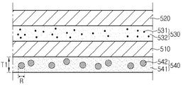
As shown in FIGS. 2 and 3, the light conversion sheet 501 includes a lower substrate 510, an upper substrate 520, a light conversion layer 530 and a light diffusion layer 540.
The lower substrate 510 is disposed under the light conversion layer 530. The lower substrate 510 is transparent and flexible. The lower substrate 510 may adhere to a bottom surface of the light conversion layer 530.
For instance, transparent polymer such as PET (polyethyleneterephthalate) can be used as a material for the lower substrate 510.
The upper substrate 520 is disposed on the light conversion layer 530. The upper substrate 520 may be transparent and flexible. The upper substrate 520 may adhere to the top surface of the light conversion layer 530.
The upper substrate 520 may include a transparent polymer such as PET.
The light conversion layer 530 is sandwiched between the upper and lower substrates 520 and 510. The upper and lower substrates 520 and 510 support the light conversion layer 530. The upper and lower substrates 520 and 510 protect the light conversion layer 530 from external physical impact.
In addition, the upper and lower substrates 520 and 510 have low oxygen permeability and low moisture permeability. Thus, the upper and lower substrates 520 and 510 can protect the light conversion layer 530 from external chemical penetration by oxygen and/or moisture.
The light conversion layer 530 is interposed between the lower and upper substrates 510 and 520. The light conversion layer 530 may adhere to the top surface of the lower substrate 510, and adhere to the bottom surface of the upper substrate 520.
The light conversion layer 530 includes a plurality of light conversion particles 531 and a first host layer 532.
The light conversion particles 531 are disposed between the lower substrate 510 and the upper substrate 520. In detail, the light conversion particles 531 are uniformly distributed in the first host layer 532 and the first host layer 532 is disposed between the lower substrate 510 and the upper substrate 520.
The light conversion particles 531 convert the wavelength of the light emitted from the light emitting diodes 400. In detail, the light conversion particles 531 receive light emitted from the light emitting diodes 400 to convert the wavelength of the incident light. For instance, the light conversion particles 531 may convert the blue light emitted from the light emitting diodes 400 into the green light and the red light. That is, a part of the light conversion particles 531 may convert the blue light into the green light having the wavelength in the range of about 520nm to about 560nm and a part of the light conversion particles 531 may convert the blue light into the red light having the wavelength in the range of about 630nm to about 660nm.
In addition, the light conversion particles 531 may convert the UV light emitted from the light emitting diodes 400 into the blue light, the green light and the red light. That is, a part of the light conversion particles 531 may convert the UV light into the blue light having the wavelength in the range of about 430nm to about 470nm, a part of the light conversion particles 531 may convert the UV light into the green light having the wavelength in the range of about 520nm to about 560nm and a part of the light conversion particles 531 may convert the UV light into the red light having the wavelength in the range of about 630nm to about 660nm.
That is, if the light emitting diodes 400 are blue light emitting diodes that emit the blue light, the light conversion particles 531 capable of converting the blue light into the green light and the red light can be employed. In addition, if the light emitting diodes are UV light emitting diodes that emit the UV light, the light conversion particles 531 capable of converting the UV light into the blue light, the green light and the red light can be employed.
The light conversion particles 531 may be prepared as quantum dots (QD). The quantum dots may include core nano-crystals and shell nano-crystals surrounding the core nano-crystals. In addition, the quantum dots may include organic ligands bonded to the shell nano-crystals. Further, the quantum dots may include an organic coating layer surrounding the shell nano-crystals.
The shell nano-crystals may be prepared as at least two layers. The shell nano-crystals are formed on the surface of the core nano-crystals. The quantum dots lengthen the wavelength of the light incident into the core nano-crystals by using the shell nano-crystals forming a shell layer, thereby improving the light efficiency.
The quantum dots may include at least one of a group-II compound semiconductor, a group-III compound semiconductor, a group-V compound semiconductor, and a group-VI compound semiconductor. In more detail, the core nano-crystals may include CdSe, InGaP, CdTe, CdS, ZnSe, ZnTe, ZnS, HgTe or HgS. In addition, the shell nano-crystals may include CuZnS, CdSe, CdTe, CdS, ZnSe, ZnTe, ZnS, HgTe or HgS. The quantum dot may have a diameter of about 1nm to about 10nm.
The wavelength of the light emitted from the quantum dots can be adjusted according to the size of the quantum dots. The organic ligand may include pyridine, mercapto alcohol, thiol, phosphine and phosphine oxide. The organic ligand may stabilize the unstable quantum dots after the synthesis process. Dangling bonds may be formed at the valence band and the quantum dots may be unstable due to the dangling bonds. However, since one end of the organic ligand is the non-bonding state, the one end of the organic ligand is bonded with the dangling bonds, thereby stabilizing the quantum dots.
In particular, if the size of the quantum dot is smaller than the Bohr radius of an exciton, which consists of an electron and a hole excited by light and electricity, the quantum confinement effect may occur, so that the quantum dot may have the discrete energy level. Thus, the size of the energy gap is changed. In addition, the charges are confined within the quantum dot, so that the light emitting efficiency can be improved.
Different from general fluorescent pigments, the fluorescent wavelength of the quantum dot may vary depending on the size of the particles. In detail, the light has the shorter wavelength as the size of the particle is reduced, so that the fluorescent light having the wavelength band of visible ray can be generated by adjusting the size of the particles. In addition, the quantum dot represents the extinction coefficient which is 100 to 1000 times higher than that of the general pigment and has the superior quantum yield as compared with the general pigment, so that strong fluorescent light can be generated.
The quantum dots can be synthesized through the chemical wet scheme. The chemical wet scheme is to grow the particles by immersing the precursor material in the organic solvent. According to the chemical wet scheme, the quantum dots can be synthesized.
The first host layer 532 surrounds the light conversion particles 531. That is, the light conversion particles 531 are uniformly distributed in the first host layer 532. The first host layer 532 may include polymer. The first host layer 532 is transparent. That is, the first host layer 532 may include transparent polymer.
The first host layer 532 is disposed between the lower substrate 510 and the upper substrate 520. The first host layer 532 may adhere to the top surface of the lower substrate 510, and adhere to the bottom surface of the upper substrate 520.
The light diffusion layer 540 is disposed under the lower substrate 510. The light diffusion layer 540 is disposed on the bottom surface of the lower substrate 510. In more detail, the light diffusion layer 540 may adhere to the bottom surface of the lower substrate 510. The light diffusion layer 540 may be coated on the entire surface of the lower substrate 510.
The light diffusion layer 540 may convert the route of the incident light. In detail, the light diffusion layer 540 can randomly covert the route of the incident light. Thus, the light diffusion layer 540 can improve the brightness uniformity of the incident light. The light diffusion layer 540 uniformly outputs the light, which is incident thereto from the light guide plate 200, to the light diffusion layer 540.
In addition, the light diffusion layer 540 may serve as a protective layer. That is, the light diffusion layer 540 as well as the lower substrate 510 may protect the light conversion layer 530 from the penetration of oxygen/moisture.
The light diffusion layer 540 may have a thickness in a range of about 5㎛ to about 100㎛. The light diffusion layer 540 includes a second host layer 541 and a light path conversion particles 542.
The second host layer 541 surrounds the light path conversion particles 542. The second host layer 541 may uniformly distribute the light path conversion particles 542.
The second host layer 541 is disposed on the bottom surface of the lower substrate 510. The second host layer 541 is coated on the bottom surface of the lower substrate 510. In detail, the second host layer 541 adheres to an entire bottom surface of the lower substrate 510.
The second host layer 541 is transparent. The second host layer 541 has a thickness T1 in a range of about 5㎛ to about 100㎛. The second host layer 541 includes transparent polymer. In detail, the second host layer 541 may include epoxy resin or silicon resin. That is, the second host layer 541 is a resin layer consisting of resin.
The light path conversion particles 542 are disposed in the second host layer 541. The light path conversion particles 542 are uniformly distributed in the second host layer 541. The light path conversion particles 542 may be disposed on the entire bottom surface of the lower substrate 510.
The light path conversion particles 542 may be transparent. The light path conversion particles 542 may have a refractive index different from that of the second host layer 541. For instance, the light path conversion particles 542 may have a refractive index higher than that of the second host layer 541. In detail, the second host layer 541 has a refractive index of about 1.2 to about 1.6 and the light path conversion particles 542 have a refractive index of about 1.3 to about 2.1. The difference of the refractive index between the light path conversion particles 542 and the second host layer 541 is in the range of about 0.05 to about 0.8.
The light path conversion particles 542 may include silicon oxide, aluminum oxide, tantalum oxide, polymethylmethacrylate (PMMA), polybutylmethacrylate (PBMA), silica, boehmite, polystyrene or titanium oxide.
The light path conversion particles 542 may have a spherical shape, a polygonal shape or a column shape. In detail, the light path conversion particles 542 may be prepared in the form of beads.
A diameter R of the light path conversion particles 542 may be smaller than the thickness T1 of the second host layer 541. For instance, the thickness T1 of the second host layer 541 is 1.1 times larger than the diameter R of the light path conversion particles 542. In detail, the thickness T1 of the second host layer 541 is 1.1 to 20 times larger than the diameter R of the light path conversion particles 542.
Referring to FIG. 4, the diameter R of the light path conversion particles 542 may be similar to the thickness T2 of the second host layer 541. The diameter R of the light path conversion particles 542 may correspond to the thickness T2 of the second host layer 541. The diameter R of the light path conversion particles 542 may be substantially equal to the thickness T2 of the second host layer 541. For instance, the thickness T2 of the second host layer 541 is about 0.9 to 1.1 times larger than the diameter R of the light path conversion particles 542.
Therefore, fine protrusions 543 may be formed in the second host layer 541 corresponding to the light path conversion particles 542. The thickness of the second host layer 541 may be determined depending on the ratio of resin composition to form the second host layer 541. In addition, the thickness T2 of the second host layer 541 may vary depending on viscosity of the resin composition.
The thickness T2 of the second host layer 541 may be in the range of about 5㎛ to about 7㎛. In addition, the diameter R of the light path conversion particles 542 may be in the range of about 5㎛ to about 7㎛.
Referring to FIG. 5, the diameter R of the light path conversion particles 542 may be larger than the thickness T3 of the second host layer 541. That is, the thickness T3 of the second host layer 541 may be significantly smaller than the diameter R of the light path conversion particles 542. For instance, the thickness T3 of the second host layer 541 may be smaller than 9/10 of the diameter R of the light path conversion particles 542. In detail, the thickness T3 of the second host layer 541 may in the range of about 6/10 to about 8/10 of the diameter R of the light path conversion particles 542.
Therefore, the protrusions 543 are formed in the second host layer 541 corresponding to the light path conversion particles 542. The thickness T3 of the second host layer 541 may be determined depending on the ratio of resin composition to form the light path conversion particles 542 and the second host layer 541. In addition, the thickness T3 of the second host layer 541 may vary depending on viscosity of the resin composition.
For instance, the second host layer 541 may have a thickness T3 of about 5㎛ or less. In detail, the second host layer 541 may have a thickness T3 of about 1.5㎛ to about 4㎛.
As shown in FIG. 6, the protrusions 543 may directly make contact with the top surface of the light guide plate 200. The bottom surface of the light conversion sheet 501 may uniformly make contact with the top surface of the light guide plate 200 by the protrusions 543. In addition, the contact area between the light conversion sheet 501 and the light guide plate 200 may be reduced by the protrusions 543. In particular, the protrusions 543 can prevent the light conversion sheet 501 from partially making contact with the light guide plate 200.
Thus, the light conversion sheet 501 and the LCD according to the embodiment may have the improved brightness uniformity.
Referring to FIG. 7, the lower substrate 510 may be omitted. That is, the light diffusion layer 540 can directly make contact with the light conversion layer 530. In detail, the second host layer 541 can directly make contact with the light diffusion layer 540. In more detail, the first host layer 532 can directly make contact with the second host layer 541.
That is, the light diffusion layer 540 can improve the brightness uniformity while sealing the light conversion layer 530. In addition, since the lower substrate 510 is omitted, the light conversion sheet 501 may have a thin thickness.
The first prism sheet 502 is provided on the diffusion sheet 502. The second prism sheet 503 is provided on the first prism sheet 502. The first prism sheet 502 and the second prism sheet 503 may improve the linearity of light passing therethrough.
The liquid crystal panel 20 is disposed on the optical sheets 500. In addition, the liquid crystal panel 20 is disposed on a panel guide. The liquid crystal panel 20 is guided by the panel guide.
The liquid crystal panel 20 displays images by adjusting intensity of light passing through the liquid crystal panel 20. In detail, the liquid crystal panel 20 is a display panel for displaying the images by using the light emitted from the backlight unit 10. The liquid crystal panel 20 includes a TFT substrate 21, a color filter substrate 22 and a liquid crystal layer interposed between the two substrates. In addition, the liquid crystal panel 20 includes polarizing filters.
Hereinafter, the TFT substrate 21 and the color filter substrate 22 will be described in detail although it is not shown in the drawings in detail. The TFT substrate 21 includes a plurality of gate lines and a plurality of data lines crossing the gate lines to define pixels and a thin film transistor (TFT) is provided at each intersection such that the thin film transistor TFT can be connected to a pixel electrode of the pixel in one-to-one correspondence. The color filter substrate 22 includes color filters having R, G and B colors corresponding to the pixels, a black matrix covering the gate lines, data lines and thin film transistors within the limit of the color filters, and a common electrode covering the above elements.
A driving PCB 25 is provided at an outer peripheral portion of the liquid crystal panel 20 to supply driving signals to the gate lines and data lines.
The driving PCB 25 is electrically connected to the liquid crystal panel 20 by a COF (chip on film) 24. The COF 24 may be replaced with a TCP (tape carrier package).
As described above, the LCD according to the embodiment includes the light diffusion layer 540 disposed under the light conversion layer 530. Thus, the light emitted from the light emitting diode 400 can be uniformly distributed through the light conversion layer 530. That is, the light incident into the light conversion layer 530 may have the improved brightness uniformity.
Therefore, the light conversion layer 530 can convert the light having the improve brightness uniformity, so the light conversion efficiency can be improved. That is, the light output from the light guide plate 200 may not be locally concentrated on the light conversion layer 530, but can be uniformly incident into the light conversion layer 530. Thus, the light conversion performance of the light conversion layer 530 can be maximized.
Since the light conversion layer 520 can improve the brightness uniformity of the light, the LCD according to the embodiment does not require an additional diffusion sheet. Thus, the LCD according to the embodiment may have the slim structure.
In addition, the light diffusion layer 540 includes the light path conversion particles 542. Further, the light diffusion layer 540 includes the protrusions 543 corresponding to the light path conversion particles 542. The protrusions 543 may protrude downward.
Especially, the protrusions 543 can directly make contact with the light guide plate 200 disposed below the protrusions 543. Due to the protrusions 543, the uniform contact area can be formed between the light conversion sheet 501 and the light guide plate 200.
Therefore, the brightness non-uniformity, which is caused due to the local contact between the light conversion sheet 510 and the light guide plate 200, can be prevented by the protrusions 543.
Thus, the LCD according to the embodiment can maximize the light conversion efficiency of the light conversion layer 530 while improving the brightness uniformity.
Hereinafter, the light emitting device according to the embodiment will be described with reference to FIGS. 8 to 11.
FIG. 8 is a perspective view showing a light emitting device package according to the embodiment, FIG. 9 is a sectional view taken along line C-C’ of FIG. 8, FIG. 10 is a sectional view showing a light emitting diode chip according to the first embodiment, and FIG. 11 is a sectional view showing a light emitting diode chip according to the second embodiment. In the description about the light emitting device package according to the embodiment, the previous description about the light conversion sheet will be incorporated by reference. That is, the previous description of the light conversion sheet may be basically incorporated herein by reference except for the modified parts.
Referring to FIGS. 8 to 11, the light emitting device package according to the embodiment includes a body 810, a plurality of lead electrodes 821 and 822, a light emitting part 830, a filling part 840, a plurality of light conversion particles 850 and a plurality of light path conversion particles 884.
The body 810 receives the light emitting part 830, the filling part 840, and the light conversion particles 850 therein and supports the lead electrodes 821 and 822.
The body 810 may be formed by using one of a resin material, such as PPA, a ceramic material, liquid crystal polymer (LCP), syndiotactic (SPS), poly phenylene ether (PPS), and a silicon material, but the embodiment is not limited thereto. The body 810 can be integrally formed through the injection molding or can be formed by laminating a plurality of layers.
The body 810 includes a cavity C having an open upper portion. The cavity C can be formed by patterning, punching, cutting or etching the body 810. In addition, the cavity C can be formed by using a metal mold having the structure equal to the structure of the cavity C when the body 810 is formed.
The cavity C may have a cup shape or a concave vessel shape. In addition, the cavity C may have a surface of a circular shape, a polygonal shape or a random shape, but the embodiment is not limited thereto.
The inner wall of the cavity C may be vertical or inclined to the bottom surface of the cavity C by taking the light distribution angle of the light emitting device package into consideration.
The body 810 may include a base part 811 and a receiving part 812.
The base part 811 supports the receiving part 812. In addition, the base part 811 supports the lead electrodes 821 and 822. For instance, the base part 811 may have a rectangular parallelepiped shape.
The receiving part 812 is disposed on the base part 811. The cavity C is defined by the receiving part 812. That is, the cavity C is a groove formed in the receiving part 812. The receiving part 812 surrounds the cavity C. When viewed from the top, the receiving part 812 may have a closed loop shape. For instance, the receiving part 812 may have a wall shape surrounding the cavity C.
The receiving part 812 includes a top surface, an outer surface and an inner surface. The inner surface is an inclined surface, which is inclined with respect to the top surface.
The lead electrodes 821 and 822 can be realized as a lead frame, but the embodiment is not limited thereto.
The lead electrodes 821 and 822 are disposed in the body 810 and installed on the bottom surface of the cavity C while being electrically isolated from each other. Outer portions of the lead electrodes 821 and 822 are exposed out of the body 810.
End portions of the lead electrodes 821 and 822 are located at one lateral side or the other lateral side of the cavity C.
The lead electrodes 821 and 822 can be prepared as lead frames, which can be formed when the body 810 is injection molded. For instance, the lead electrodes 821 and 822 include a first lead electrode 821 and a second lead electrode 822.
The first lead electrode 821 is spaced apart from the second lead electrode 822. In addition, the first lead electrode 821 and the second lead electrode 822 are electrically connected to the light emitting part 830.
The light emitting part 830 includes at least one light emitting diode chip. For instance, the light emitting part 830 may include a blue light emitting diode chip or a UV light emitting diode chip.
The light emitting part 830 may be a lateral type light emitting diode chip or a vertical type light emitting diode chip. As shown in FIG. 11, the light emitting part 830 may include a conductive substrate 831, a light reflective layer 832, a first conductive semiconductor layer 833, a second conductive semiconductor layer 834, an active layer 835 and a second electrode 836.
The conductive substrate 831 consists of a conductor. The conductive substrate 831 supports the light reflective layer 832, the first conductive semiconductor layer 833, the second conductive semiconductor layer 834, the active layer 835 and the second electrode 836.
The conductive substrate 831 is connected to the first conductive semiconductor layer 833 through the light reflective layer 832. That is, the conductive substrate 831 serves as a first electrode for supplying an electric signal to the first conductive semiconductor layer 833.
The light reflective layer 832 is disposed on the conductive substrate 831. The light reflective layer 832 reflects the light emitted from the active layer 835 in the upward direction. In addition, the light reflective layer 832 is a conductive layer. Thus, the light reflective layer 832 connects the conductive substrate 831 to the first conductive semiconductor layer 833. The light reflective layer 832 may be formed by using a metal, such as Ag or Al.
The first conductive semiconductor layer 833 is formed on the light reflective layer 832. The first conductive semiconductor layer 833 has a first conductive type. The first conductive semiconductor layer 833 is an N type semiconductor layer. For instance, the first conductive semiconductor layer 833 is an N type GaN layer.
The second conductive semiconductor layer 834 is formed on the first conductive semiconductor layer 833. The second conductive semiconductor layer 834 is a P type semiconductor layer facing the first conductive semiconductor layer 833. For instance, the second conductive semiconductor layer 834 is a P type GaN layer.
The active layer 835 is interposed between the first conductive semiconductor layer 833 and the second conductive semiconductor layer 834. The active layer 835 may have a single quantum well structure or a multiple quantum wall structure. The active layer 835 may have a periodicity of an InGaN well layer and an AlGaN barrier layer or an InGaN well layer and a GaN barrier layer. The light emitting material for the active layer 835 may vary depending on the light emission wavelengths, such as the blue, red and green wavelengths.
The second electrode 836 is formed on the second conductive semiconductor layer 834. The second electrode 836 is connected to the second conductive semiconductor layer 834.
Meanwhile, the light emitting part 830 may be a lateral type LED. An additional wire may be necessary to connect the lateral type LED to the first lead electrode 821.
The light emitting part 830 is connected to the first lead electrode 821 through a bump and connected to the second lead electrode 822 through a wire. In particular, the light emitting part 830 can be directly formed on the first lead electrode 821.
Besides the above, the light emitting part 830 can be connected to the first and second lead electrodes 821 and 822 through the wire bonding, the die bonding or the flip bonding scheme, but the embodiment is not limited thereto.
The filling part 840 is formed in the cavity C. The filling part 840 is transparent. The filling part 840 may include a material, such as silicon or epoxy, or a material having the refractive index of 2 or less. The filling part 840 covers the light emitting part 830. The filling part 840 may directly make contact with the light emitting part 830.
A reflective layer can be formed on the inner wall of the cavity C. The reflective layer may include a material having high reflective property, such as white PSR (photo solder resist) ink, Ag or Al.
As shown in FIGS. 9 and 10, the light conversion member 880 is formed on the surface of the filling part 840 in the form of a sheet, that is, in the form of the layered structure. In detail, the solution including the host 881 and the light conversion particles 882 is coated on the filling part 840 in a state in which the solvent is not removed,, and then the solvent is evaporated. Thus, the light conversion member 880 is formed as the layered structure.
The light conversion member 880 is substantially identical to the light conversion sheet that has been described above. That is, the light conversion member 880 includes a light conversion layer including a plurality of light conversion particles to convert the wavelength of the light emitted from a light source; and a light diffusion layer disposed before the light conversion layer on the basis of the light path from the light source and including a plurality of light path conversion particles. The light conversion member 880 may include a plurality of protrusions protruding toward the optical member.
That is, the light conversion member includes a light conversion layer having a first host 881 and a plurality of light conversion particles 882 distributed in the first host, a second host 883 and a plurality of light path conversion particles 884 distributed in the second host.
The light conversion member according to the previous embodiments can be applied to the light conversion member 880 of the light emitting device according to the present embodiment, so the detailed description thereof will be omitted.
The light conversion particles 882 can convert may convert the blue light emitted from the light emitting part 830 into the green light. In detail, the light conversion particles 882 may convert the blue light emitted from the light emitting part 830 into the light having the wavelength band in the range of about 500nm to about 599nm.
In addition, the light conversion particles 882 may convert the blue light emitted from the light emitting part 830 into the green light. In detail, the light conversion particles 882 may convert the blue light emitted from the light emitting part 830 into the light having the wavelength band in the range of about 600nm to about 700nm.
Further, when the light emitting part 830 emits the UV light, the light conversion particles 882 may convert the radiant UV light into the blue light.
That is, the light conversion particles 882 receive the light emitted from the light emitting part 830 and convert the wavelength of the light. As described above, the light conversion particles 882 can convert the incident blue light into the green light and red light.
In addition, the light conversion particles 882 can convert the UV light emitted from the light emitting part 830 into the blue light, the green light and red light.
Thus, the white light can be generated by the light converted by the light conversion particles 882 and the light which is not converted by the light conversion particles 882. That is, the white light can be emitted through the combination of the blue light, green light and red light.
Hereinafter, the lighting device according to the embodiment will be described with reference to FIG. 12.
FIG. 12 is a perspective view showing the lighting device according to the embodiment. Referring to FIG. 12, the lighting device 900 includes a case 910, a light emitting module 930 installed in the case 910, and a connection terminal 920 installed in the case 910 to receive power from an external power source.
Preferably, the case 910 includes a material having superior heat dissipation property. For instance, the case 910 includes a metallic material or a resin material.
The light emitting module 930 may include a substrate 932 and light emitting device packages 931 according to the embodiment, which are installed on the substrate 932. The light emitting device packages 931 are spaced apart from each other or arranged in the form of a matrix. The light emitting device packages 931 can be basically incorporated with the light emitting device that has been previously described with reference to FIGS. 8 to 11.
The light emitting device package may include a light conversion member including a light conversion layer having a plurality of light conversion particles to convert the wavelength of the light emitted from a light source; and a light diffusion layer disposed before the light conversion layer on the basis of the light path from the light source and including a plurality of light path conversion particles. In addition, the light emitting device package may include an optical member including a plurality of protrusions.
That is, the light conversion member includes a light conversion layer having a first host 881 and a plurality of light conversion particles 882 distributed in the first host, a second host 883 and a plurality of light path conversion particles 884 distributed in the second host.
The substrate 932 includes an insulating member printed with a circuit pattern. For instance, the substrate 932 includes a PCB (printed circuit board), an MC (metal core) PCB, an FPCB (flexible PCB), a ceramic PCB, and an FR-4 substrate.
In addition, the substrate 932 may include a material that effectively reflects the light. A coating layer can be formed on the surface of the substrate 932. At this time, the coating layer has a white color or a silver color to effectively reflect the light.
At least one light emitting device package 931 is installed on the substrate 932. Each light emitting device package 931 may include at least one LED (light emitting diode) chip. The LED chip may include an LED that emits the light of visible ray band having red, green, blue or white color and a UV (ultraviolet) LED that emits UV light.
The light emitting device packages 931 of the light emitting module 930 can be variously combined to provide various colors and brightness. For instance, the white LED, the red LED and the green LED can be combined to achieve the high color rendering index (CRI).
The connection terminal 920 is electrically connected to the light emitting module 930 to supply power to the light emitting module 930. The connection terminal 920 has a shape of a socket screw-coupled with the external power source, but the embodiment is not limited thereto. For instance, the connection terminal 920 can be prepared in the form of a pin inserted into the external power source or connected to the external power source through a wire.
That is, the optical member and the light emitting device described above can be employed in the lighting device.
Any reference in this specification to “one embodiment,” “an embodiment,” “example embodiment,” etc., means that a particular feature, structure, or characteristic described in connection with the embodiment is included in at least one embodiment of the invention. The appearances of such phrases in various places in the specification are not necessarily all referring to the same embodiment. Further, when a particular feature, structure, or characteristic is described in connection with any embodiment, it is submitted that it is within the purview of one skilled in the art to effects such feature, structure, or characteristic in connection with other ones of the embodiments.
Although embodiments have been described with reference to a number of illustrative embodiments thereof, it should be understood that numerous other modifications and embodiments can be devised by those skilled in the art that will fall within the spirit and scope of the principles of this disclosure. More particularly, various variations and modifications are possible in the component parts and/or arrangements of the subject combination arrangement within the scope of the disclosure, the drawings and the appended claims. In addition to variations and modifications in the component parts and/or arrangements, alternative uses will also be apparent to those skilled in the art.
Claims (20)
- An optical member comprising:a light conversion layer including a plurality of light conversion particles; anda light diffusion layer including a plurality of light path conversion particles under the light conversion layer.
- The optical member of claim 1, wherein the light conversion layer includes a first host layer surrounding the light conversion particles and the light diffusion layer includes a second host layer surrounding the light path conversion particles.
- The optical member of claim 2, wherein the light path conversion particles have a diameter smaller than a thickness of the second host layer.
- The optical member of claim 2, wherein the light path conversion particles have a diameter larger than a thickness of the second host layer.
- The optical member of claim 1, wherein the light diffusion layer is provided with protrusions corresponding to the light path conversion particles, respectively.
- The optical member of claim 2, wherein the light path conversion particles have a diameter, which is 0.9 to 1.1 times larger than a thickness of the second host layer.
- The optical member of claim 1, wherein the light conversion layer directly makes contact with the light diffusion layer.
- A display device comprising:a light source;a light conversion member into which light is incident from the light source; anda display panel into which the light is incident from the light conversion member,wherein the light conversion member comprises:a light conversion layer including a plurality of light conversion particles to convert a wavelength of the light emitted from the light source; anda light diffusion layer disposed before the light conversion layer on a basis of a path of the light from the light source and including a plurality of light path conversion particles.
- The display device of claim 8, wherein the light path conversion particles have a diameter in a range of about 5㎛ to about 7㎛.
- The display device of claim 8, wherein the light conversion layer includes a first host layer surrounding the light conversion particles and the light diffusion layer includes a second host layer surrounding the light path conversion particles.
- The display device of claim 10, wherein the light path conversion particles include silicon oxide, aluminum oxide, tantalum oxide, polymethylmethacrylate (PMMA), polybutylmethacrylate (PBMA), silica, boehmite, polystyrene or titanium oxide.
- The display device of claim 10, wherein a difference in refractive index between the second host layer and the light path conversion particle is in a range of about 0.05 to about 0.8.
- A display device comprising:a light source;an optical member into which light is incident from the light source;a light conversion member on the optical member; anda display panel on the light conversion member,wherein the light conversion member includes a plurality of protrusions protruding toward the optical member.
- The display device of claim 13, wherein the light conversion member includes a plurality of beads corresponding to the protrusions, respectively.
- The display device of claim 13, wherein the optical member guide the light from the light source to the light conversion member, and the protrusions directly make contact with a top surface of the optical member.
- The display device of claim 14, wherein the light conversion member includes a light conversion layer disposed on the beads.
- The display device of claim 16, wherein the light conversion member includes a transparent resin layer surrounding the beads, and the beads have a refractive index higher than a refractive index of the resin layer.
- The display device of claim 17, wherein beads have the refractive index in a range of about 1.3 t about 2.1 and the resin layer have the refractive index in the range of about 1.2 to about 1.6.
- A light emitting device comprising:a light emitting part;an optical member disposed in a path of light emitted from the light emitting part; anda light conversion member comprising a light conversion layer including a plurality of light conversion particles to convert a wavelength of the light emitted from the light emitting part and a light diffusion layer disposed before the light conversion layer on a basis of a path of the light from the light emitting part and including a plurality of light path conversion particles.
- A light emitting device comprising:a light emitting part;an optical member disposed in a path of light emitted from the light emitting part; anda light conversion member including a plurality of protrusions protruding toward the optical member.
Priority Applications (3)
| Application Number | Priority Date | Filing Date | Title |
|---|---|---|---|
| EP12848185.0A EP2776875B1 (en) | 2011-11-07 | 2012-08-08 | Display device having a light conversion member |
| CN201280066300.9A CN104040382B (en) | 2011-11-07 | 2012-08-08 | Optical sheet and there is display device and the light-emitting device of this optical sheet |
| US14/356,657 US10247871B2 (en) | 2011-11-07 | 2012-08-08 | Optical sheet, display device and light emitting device having the same |
Applications Claiming Priority (2)
| Application Number | Priority Date | Filing Date | Title |
|---|---|---|---|
| KR10-2011-0115394 | 2011-11-07 | ||
| KR1020110115394A KR101251815B1 (en) | 2011-11-07 | 2011-11-07 | Optical sheet and display device having the same |
Publications (1)
| Publication Number | Publication Date |
|---|---|
| WO2013069878A1 true WO2013069878A1 (en) | 2013-05-16 |
Family
ID=48290213
Family Applications (1)
| Application Number | Title | Priority Date | Filing Date |
|---|---|---|---|
| PCT/KR2012/006308 WO2013069878A1 (en) | 2011-11-07 | 2012-08-08 | Optical sheet, display device and light emitting device having the same |
Country Status (6)
| Country | Link |
|---|---|
| US (1) | US10247871B2 (en) |
| EP (1) | EP2776875B1 (en) |
| KR (1) | KR101251815B1 (en) |
| CN (2) | CN104040382B (en) |
| TW (2) | TW201625479A (en) |
| WO (1) | WO2013069878A1 (en) |
Families Citing this family (36)
| Publication number | Priority date | Publication date | Assignee | Title |
|---|---|---|---|---|
| US9803833B2 (en) * | 2013-12-03 | 2017-10-31 | X Development Llc | Multi-aperture illumination layer for tileable display |
| KR20150076883A (en) * | 2013-12-27 | 2015-07-07 | 삼성디스플레이 주식회사 | Display apparatus |
| CN105090808B (en) | 2014-05-13 | 2017-08-29 | 扬升照明股份有限公司 | Backlight module |
| US10642087B2 (en) | 2014-05-23 | 2020-05-05 | Eyesafe, Llc | Light emission reducing compounds for electronic devices |
| JP6295237B2 (en) * | 2014-09-30 | 2018-03-14 | 富士フイルム株式会社 | Backlight unit, liquid crystal display device, and wavelength conversion member |
| CN115291434A (en) * | 2014-09-30 | 2022-11-04 | 富士胶片株式会社 | Backlight unit, liquid crystal display device, and wavelength conversion member |
| CN104566232B (en) * | 2015-01-09 | 2017-10-27 | 张家港康得新光电材料有限公司 | Luminous film layer structure, its preparation method and backlight |
| JP2016167041A (en) * | 2015-03-03 | 2016-09-15 | 大日本印刷株式会社 | High color rendering liquid crystal display device and color filter |
| CN104791662B (en) * | 2015-04-16 | 2018-05-29 | 青岛海信电器股份有限公司 | A kind of side entering type display module and display device |
| CN104728779B (en) * | 2015-04-21 | 2018-01-12 | 张家港康得新光电材料有限公司 | luminous film layer structure and backlight module |
| JP2017027872A (en) * | 2015-07-27 | 2017-02-02 | ソニー株式会社 | Display device |
| KR101746722B1 (en) * | 2016-01-20 | 2017-06-13 | 에스케이씨하스디스플레이필름(유) | Liquid crystal display comprising quantum dot sheet and color gamut enhancing film |
| CN105867019A (en) * | 2016-03-30 | 2016-08-17 | 苏州星烁纳米科技有限公司 | Wavelength conversion element, backlight module and display device |
| KR102155405B1 (en) * | 2016-04-15 | 2020-09-14 | 주식회사 엘지화학 | Light guide plate unit, back light unit and liquid crystal display comprising the same |
| CN109819683A (en) | 2016-10-07 | 2019-05-28 | 索尼公司 | Light emitting device, display device and lighting device |
| KR20180042508A (en) * | 2016-10-17 | 2018-04-26 | 삼성디스플레이 주식회사 | Color conversion panel and display device including the same |
| CN106501999A (en) * | 2016-11-11 | 2017-03-15 | 张家港海纳至精新材料科技有限公司 | Blooming group and backlight module |
| KR102589156B1 (en) * | 2016-12-28 | 2023-10-12 | 엘지디스플레이 주식회사 | Light source module, back light unit and liquid crystal display device using the same |
| CN107479251A (en) * | 2017-08-21 | 2017-12-15 | 深圳市华星光电技术有限公司 | Fluorescent powder film and backlight module |
| US10957825B2 (en) | 2017-09-25 | 2021-03-23 | Lg Innotek Co., Ltd. | Lighting module and lighting apparatus having thereof |
| CN109681846B (en) * | 2017-10-18 | 2021-01-05 | 深圳光峰科技股份有限公司 | Wavelength conversion device and preparation method thereof |
| CN107701935A (en) * | 2017-10-19 | 2018-02-16 | 常州工学院 | A kind of LED flexible light-conductings device |
| TWI640972B (en) * | 2017-12-14 | 2018-11-11 | 宏齊科技股份有限公司 | Display device and light source module thereof |
| CN109946778A (en) * | 2017-12-21 | 2019-06-28 | 张家港康得新光电材料有限公司 | Optical diaphragm and ambient light sensor with it |
| CN108279460B (en) * | 2018-01-03 | 2020-01-21 | 上海中航光电子有限公司 | Quantum dot light guide plate, backlight module and display device |
| US20190219874A1 (en) * | 2018-01-16 | 2019-07-18 | Huizhou China Star Optoelectronics Technology Co., Ltd. | Backlight module and display device |
| CN110094647A (en) * | 2018-01-29 | 2019-08-06 | 深圳市绎立锐光科技开发有限公司 | A kind of Wavelength converter, luminescence component and lighting device |
| KR20200128704A (en) * | 2018-03-07 | 2020-11-16 | 도판 인사츠 가부시키가이샤 | Optical film, optical barrier film, and backlight unit |
| CN108803141A (en) * | 2018-06-21 | 2018-11-13 | 惠州市华星光电技术有限公司 | Quantum dot integrates optical module, backlight module and liquid crystal display |
| US11810532B2 (en) | 2018-11-28 | 2023-11-07 | Eyesafe Inc. | Systems for monitoring and regulating harmful blue light exposure from digital devices |
| US11592701B2 (en) | 2018-11-28 | 2023-02-28 | Eyesafe Inc. | Backlight unit with emission modification |
| US10955697B2 (en) | 2018-11-28 | 2021-03-23 | Eyesafe Inc. | Light emission modification |
| KR102577764B1 (en) * | 2019-03-19 | 2023-09-14 | 삼성디스플레이 주식회사 | Display device and method for manufacturing display device |
| KR20210136720A (en) * | 2020-05-08 | 2021-11-17 | 삼성전자주식회사 | A light-generating device |
| KR20230143917A (en) * | 2021-02-17 | 2023-10-13 | 아이세이프 잉크. | Backlight unit with emission modification function |
| WO2023224189A1 (en) * | 2022-05-19 | 2023-11-23 | 엘지전자 주식회사 | Display device |
Citations (4)
| Publication number | Priority date | Publication date | Assignee | Title |
|---|---|---|---|---|
| KR20060129835A (en) * | 2005-06-13 | 2006-12-18 | 삼성전자주식회사 | Backlight assembly and liquid crystal display apparatus having the same |
| KR20070092440A (en) * | 2006-03-10 | 2007-09-13 | (주)케이디티 | Photoluminescent sheet |
| KR20080063986A (en) * | 2007-01-03 | 2008-07-08 | 삼성전기주식회사 | Diffusion sheet for wavelength changing and backlight unit using the same |
| KR20100047841A (en) * | 2007-07-18 | 2010-05-10 | 큐디 비젼, 인크. | Quantum dot-based light sheets useful for solid-state lighting |
Family Cites Families (118)
| Publication number | Priority date | Publication date | Assignee | Title |
|---|---|---|---|---|
| JP3931355B2 (en) | 1995-09-06 | 2007-06-13 | 日亜化学工業株式会社 | Planar light source |
| TW383508B (en) * | 1996-07-29 | 2000-03-01 | Nichia Kagaku Kogyo Kk | Light emitting device and display |
| US6608332B2 (en) * | 1996-07-29 | 2003-08-19 | Nichia Kagaku Kogyo Kabushiki Kaisha | Light emitting device and display |
| US20050146258A1 (en) | 1999-06-02 | 2005-07-07 | Shimon Weiss | Electronic displays using optically pumped luminescent semiconductor nanocrystals |
| JP4573946B2 (en) * | 2000-05-16 | 2010-11-04 | 株式会社きもと | Light diffusing sheet |
| KR100867066B1 (en) | 2000-09-25 | 2008-11-04 | 미츠비시 레이온 가부시키가이샤 | Surface light source device |
| US6723478B2 (en) | 2000-12-08 | 2004-04-20 | Hitachi, Ltd. | Color filter and liquid crystal display provided therewith |
| US6930737B2 (en) * | 2001-01-16 | 2005-08-16 | Visteon Global Technologies, Inc. | LED backlighting system |
| US6697130B2 (en) * | 2001-01-16 | 2004-02-24 | Visteon Global Technologies, Inc. | Flexible led backlighting circuit |
| US20030066998A1 (en) | 2001-08-02 | 2003-04-10 | Lee Howard Wing Hoon | Quantum dots of Group IV semiconductor materials |
| US6806642B2 (en) * | 2001-09-04 | 2004-10-19 | Durel Corporation | Light source with cascading dyes and BEF |
| JP2003255562A (en) | 2002-03-04 | 2003-09-10 | Sharp Corp | Pattern forming method and display using the same |
| TWI292961B (en) | 2002-09-05 | 2008-01-21 | Nichia Corp | Semiconductor device and an optical device using the semiconductor device |
| JP4072632B2 (en) * | 2002-11-29 | 2008-04-09 | 豊田合成株式会社 | Light emitting device and light emitting method |
| JP4085379B2 (en) | 2003-03-28 | 2008-05-14 | ミネベア株式会社 | Surface lighting device |
| JP2004315661A (en) | 2003-04-16 | 2004-11-11 | Mitsubishi Chemicals Corp | Semiconductor ultramicroparticle and electroluminescent element |
| US7040774B2 (en) | 2003-05-23 | 2006-05-09 | Goldeneye, Inc. | Illumination systems utilizing multiple wavelength light recycling |
| JP2005128140A (en) * | 2003-10-22 | 2005-05-19 | Dainippon Ink & Chem Inc | Optical sheet and backlight unit using the same |
| JP4339672B2 (en) * | 2003-11-28 | 2009-10-07 | 大日本印刷株式会社 | Light diffusion sheet |
| US7517728B2 (en) | 2004-03-31 | 2009-04-14 | Cree, Inc. | Semiconductor light emitting devices including a luminescent conversion element |
| US20060034084A1 (en) | 2004-06-28 | 2006-02-16 | Kyocera Corporation | Light-emitting apparatus and illuminating apparatus |
| US7255469B2 (en) | 2004-06-30 | 2007-08-14 | 3M Innovative Properties Company | Phosphor based illumination system having a light guide and an interference reflector |
| JP2006054088A (en) | 2004-08-11 | 2006-02-23 | Alps Electric Co Ltd | Surface light-emitting device and liquid crystal display device |
| KR20060030350A (en) | 2004-10-05 | 2006-04-10 | 삼성전자주식회사 | White light generating unit, backlight assembly having the same and liquid crystal display apparatus having the same |
| CN1758114A (en) | 2004-10-09 | 2006-04-12 | 台达电子工业股份有限公司 | Backlight module |
| DE102005063433B4 (en) * | 2004-10-29 | 2009-11-26 | Lg Display Co., Ltd. | Backlight unit and liquid crystal display device |
| US7481562B2 (en) | 2004-11-18 | 2009-01-27 | Avago Technologies Ecbu Ip (Singapore) Pte. Ltd. | Device and method for providing illuminating light using quantum dots |
| KR100735148B1 (en) | 2004-11-22 | 2007-07-03 | (주)케이디티 | Backlight unit by phosphorescent diffusion sheet |
| KR100637201B1 (en) | 2004-12-20 | 2006-10-23 | 삼성에스디아이 주식회사 | Organic electroluminescence display and manufacturing method thereof |
| US7316497B2 (en) | 2005-03-29 | 2008-01-08 | 3M Innovative Properties Company | Fluorescent volume light source |
| KR100681521B1 (en) | 2005-04-06 | 2007-02-09 | (주)케이디티 | Backlight unit |
| KR101129434B1 (en) | 2005-04-26 | 2012-03-27 | 삼성전자주식회사 | Display device |
| JPWO2006120895A1 (en) | 2005-05-12 | 2008-12-18 | 出光興産株式会社 | Color conversion material composition and color conversion medium containing the same |
| US7632000B2 (en) * | 2005-05-25 | 2009-12-15 | Samsung Electronics Co., Ltd. | Backlight assembly and liquid crystal display device having the same |
| KR101082898B1 (en) | 2005-05-25 | 2011-11-11 | 삼성전자주식회사 | Backlight assembly and liquid crystal display apparatus having the same |
| JP4579065B2 (en) | 2005-06-23 | 2010-11-10 | セイコーインスツル株式会社 | Illumination device and display device including the same |
| US20060268537A1 (en) * | 2005-05-31 | 2006-11-30 | Makoto Kurihara | Phosphor film, lighting device using the same, and display device |
| JP4469307B2 (en) | 2005-05-31 | 2010-05-26 | セイコーインスツル株式会社 | Display device |
| WO2007103310A2 (en) | 2006-03-07 | 2007-09-13 | Qd Vision, Inc. | An article including semiconductor nanocrystals |
| CN1881034A (en) | 2005-06-15 | 2006-12-20 | 精工电子有限公司 | Color display unit |
| DE102005061828B4 (en) | 2005-06-23 | 2017-05-24 | Osram Opto Semiconductors Gmbh | Wavelength-converting converter material, light-emitting optical component and method for its production |
| KR20070002210A (en) * | 2005-06-30 | 2007-01-05 | 삼성전자주식회사 | Plate-type fluorescent lamp and display device having the same |
| TW200707025A (en) | 2005-07-08 | 2007-02-16 | Toshiba Kk | Backlight and liquid crystal display using the same |
| KR100665219B1 (en) * | 2005-07-14 | 2007-01-09 | 삼성전기주식회사 | Wavelengt-converted light emitting diode package |
| JP4771837B2 (en) | 2005-11-28 | 2011-09-14 | 京セラ株式会社 | Wavelength converter and light emitting device |
| US7859185B2 (en) * | 2006-01-24 | 2010-12-28 | Koninklijke Philips Electronics N.V. | Light-emitting device |
| WO2007086279A1 (en) | 2006-01-27 | 2007-08-02 | Konica Minolta Medical & Graphic, Inc. | Semiconductor nanoparticles and process for production thereof |
| KR20070079204A (en) * | 2006-02-01 | 2007-08-06 | 삼성전자주식회사 | Manufacturing method of optical plate, optical plate therefrom and liquid crystal display device having optical plate |
| KR100867519B1 (en) * | 2006-02-02 | 2008-11-07 | 삼성전기주식회사 | Light emitting diode module |
| JP4931628B2 (en) * | 2006-03-09 | 2012-05-16 | セイコーインスツル株式会社 | Illumination device and display device including the same |
| KR100728940B1 (en) * | 2006-03-10 | 2007-06-14 | (주)케이디티 | Photoluminescent sheet |
| KR100746749B1 (en) * | 2006-03-15 | 2007-08-09 | (주)케이디티 | Photoluminescent diffusion sheet |
| US7731377B2 (en) * | 2006-03-21 | 2010-06-08 | Semiconductor Energy Laboratory Co., Ltd. | Backlight device and display device |
| EP1998599A4 (en) | 2006-03-23 | 2010-12-08 | Idemitsu Kosan Co | Light emitting device |
| JP2007273562A (en) | 2006-03-30 | 2007-10-18 | Toshiba Corp | Semiconductor light-emitting device |
| TWI336013B (en) | 2006-04-04 | 2011-01-11 | Wintek Corp | Color liquid crystal display |
| US20070263408A1 (en) | 2006-05-09 | 2007-11-15 | Chua Janet Bee Y | Backlight module and method of making the module |
| KR101340437B1 (en) * | 2006-09-25 | 2013-12-11 | 삼성디스플레이 주식회사 | Back cover used in display device, back light assembly and display device having the same |
| KR20080043541A (en) * | 2006-11-14 | 2008-05-19 | 삼성에스디아이 주식회사 | Display device |
| US20100079701A1 (en) * | 2006-12-08 | 2010-04-01 | Yoshiaki Murayama | Lens sheet, surface light source device, and liquid crystal display device |
| KR100862532B1 (en) * | 2007-03-13 | 2008-10-09 | 삼성전기주식회사 | Method of manufacturing light emitting diode package |
| KR101686669B1 (en) | 2007-03-19 | 2016-12-14 | 나노시스, 인크. | Methods for encapsulating nanocrystals |
| US20100155749A1 (en) | 2007-03-19 | 2010-06-24 | Nanosys, Inc. | Light-emitting diode (led) devices comprising nanocrystals |
| US20100110728A1 (en) | 2007-03-19 | 2010-05-06 | Nanosys, Inc. | Light-emitting diode (led) devices comprising nanocrystals |
| WO2008144673A2 (en) | 2007-05-17 | 2008-11-27 | Spudnik, Inc. | Multilayered screens with light-emitting stripes for scanning beam display systems |
| JP4976196B2 (en) | 2007-05-18 | 2012-07-18 | セイコーインスツル株式会社 | Display device and lighting device |
| US7859175B2 (en) | 2007-05-18 | 2010-12-28 | Seiko Instruments Inc. | Illuminating device, display device and optical film |
| TW200848809A (en) | 2007-06-04 | 2008-12-16 | Ching-Bin Lin | Light guide plate and backlight module capable of converting light source wavelength and enhancing light uniformity |
| US8585273B2 (en) | 2007-07-31 | 2013-11-19 | Rambus Delaware Llc | Illumination assembly including wavelength converting material |
| JP5019289B2 (en) | 2007-08-10 | 2012-09-05 | オリンパス株式会社 | Fiber optic lighting equipment |
| WO2009022284A1 (en) | 2007-08-16 | 2009-02-19 | Koninklijke Philips Electronics N.V. | Lighting assembly |
| KR101361908B1 (en) | 2007-08-29 | 2014-02-12 | 엘지디스플레이 주식회사 | Backlight unit and liquid crystal display device having the same |
| DE102008012316B4 (en) | 2007-09-28 | 2023-02-02 | OSRAM Opto Semiconductors Gesellschaft mit beschränkter Haftung | Semiconductor light source with a primary radiation source and a luminescence conversion element |
| JP4613947B2 (en) | 2007-12-07 | 2011-01-19 | ソニー株式会社 | Illumination device, color conversion element, and display device |
| JP5280106B2 (en) | 2007-12-07 | 2013-09-04 | デクセリアルズ株式会社 | Light source device and display device |
| TW200939534A (en) | 2008-03-14 | 2009-09-16 | Forhouse Corp | LED light source module |
| US8337032B2 (en) | 2008-03-26 | 2012-12-25 | Panasonic Corporation | Semiconductor light-emitting apparatus |
| JP5418762B2 (en) | 2008-04-25 | 2014-02-19 | ソニー株式会社 | Light emitting device and display device |
| US9022632B2 (en) * | 2008-07-03 | 2015-05-05 | Samsung Electronics Co., Ltd. | LED package and a backlight unit unit comprising said LED package |
| JP4633147B2 (en) | 2008-07-22 | 2011-02-16 | 三菱電機株式会社 | Surface light source device |
| US8459855B2 (en) | 2008-07-28 | 2013-06-11 | Munisamy Anandan | UV LED based color pixel backlight incorporating quantum dots for increasing color gamut of LCD |
| JP2010061708A (en) | 2008-09-01 | 2010-03-18 | Showa Denko Kk | Method of manufacturing magnetic recording medium, and magnetic recording/reproducing apparatus |
| KR100982991B1 (en) | 2008-09-03 | 2010-09-17 | 삼성엘이디 주식회사 | Quantum dot-wavelength conversion device, preparing method of the same and light-emitting device comprising the same |
| JP5440064B2 (en) | 2008-10-21 | 2014-03-12 | 東芝ライテック株式会社 | Lighting device |
| KR101577300B1 (en) | 2008-10-28 | 2015-12-15 | 삼성디스플레이 주식회사 | Light Emitting Diode Using Quantum Dot And Backlight Assembly Having The Same |
| EP2381495B1 (en) | 2008-12-19 | 2017-04-26 | Samsung Electronics Co., Ltd. | Light emitting device package |
| JP5717949B2 (en) * | 2009-01-26 | 2015-05-13 | デクセリアルズ株式会社 | Optical member and display device |
| US7828453B2 (en) | 2009-03-10 | 2010-11-09 | Nepes Led Corporation | Light emitting device and lamp-cover structure containing luminescent material |
| US7972023B2 (en) | 2009-03-10 | 2011-07-05 | Nepes Led Corporation | Lamp-cover structure containing luminescent material |
| US20110044046A1 (en) | 2009-04-21 | 2011-02-24 | Abu-Ageel Nayef M | High brightness light source and illumination system using same |
| KR101328783B1 (en) * | 2009-05-26 | 2013-11-13 | 엘지디스플레이 주식회사 | Liquid crystal display |
| KR101068866B1 (en) | 2009-05-29 | 2011-09-30 | 삼성엘이디 주식회사 | wavelength conversion sheet and light emitting device using the same |
| TW201044067A (en) | 2009-06-01 | 2010-12-16 | Chi Mei Optoelectronics Corp | Backlight module and liquid crystal display |
| JP5238618B2 (en) | 2009-06-12 | 2013-07-17 | スタンレー電気株式会社 | Semiconductor light emitting device |
| JP5255527B2 (en) * | 2009-07-03 | 2013-08-07 | デクセリアルズ株式会社 | Color conversion member and display device |
| US9048404B2 (en) * | 2009-07-06 | 2015-06-02 | Zhuo Sun | Thin flat solid state light source module |
| KR20110012246A (en) | 2009-07-30 | 2011-02-09 | 엘지이노텍 주식회사 | Backlight unit |
| KR101508284B1 (en) | 2009-12-15 | 2015-04-06 | 엘지이노텍 주식회사 | Back Light Unit Using Quantum Dots and Liquid Display Device Comprising of the Same |
| US8545083B2 (en) | 2009-12-22 | 2013-10-01 | Sumita Optical Glass, Inc. | Light-emitting device, light source and method of manufacturing the same |
| TWI398700B (en) | 2009-12-30 | 2013-06-11 | Au Optronics Corp | Display device with quantum dot phosphor and manufacturing method thereof |
| CN201803317U (en) * | 2010-01-12 | 2011-04-20 | 金芃 | Direct type light guide plate, with groove at the bottom, of LED backlight module |
| CN103038567A (en) * | 2010-04-16 | 2013-04-10 | 弗莱克斯照明第二有限责任公司 | Illumination device comprising a film-based lightguide |
| KR101636441B1 (en) | 2010-04-23 | 2016-07-06 | 삼성전자주식회사 | Color filter and display device employing the same |
| KR101701835B1 (en) | 2010-06-29 | 2017-02-02 | 엘지전자 주식회사 | Mobile terminal |
| CN101975371B (en) | 2010-09-09 | 2013-01-30 | 友达光电股份有限公司 | Lower diffusion film, backlight module and display |
| TWI407199B (en) * | 2010-10-29 | 2013-09-01 | Au Optronics Corp | Flat panel display structure and manufacturing method thereof |
| EP2638321B1 (en) * | 2010-11-10 | 2019-05-08 | Nanosys, Inc. | Quantum dot films, lighting devices, and lighting methods |
| KR101272993B1 (en) | 2010-12-21 | 2013-06-10 | 엘지이노텍 주식회사 | Display device and method for fabricating light transforming member |
| TW201227092A (en) * | 2010-12-31 | 2012-07-01 | Ind Tech Res Inst | Mixing light module |
| KR101210180B1 (en) | 2011-04-21 | 2012-12-07 | 엘지이노텍 주식회사 | Optical member and method for fabricating the same |
| KR20130009020A (en) | 2011-07-14 | 2013-01-23 | 엘지이노텍 주식회사 | Optical member, display device having the same and method of fabricating the same |
| KR101273127B1 (en) | 2011-07-14 | 2013-06-13 | 엘지이노텍 주식회사 | Optical member, display device having the same and method of fabricating the same |
| KR101262541B1 (en) | 2011-07-18 | 2013-05-08 | 엘지이노텍 주식회사 | Display device |
| KR101893494B1 (en) | 2011-07-18 | 2018-08-30 | 엘지이노텍 주식회사 | Optical member and display device having the same |
| KR101823684B1 (en) | 2011-07-18 | 2018-01-30 | 엘지이노텍 주식회사 | Display device |
| KR101294415B1 (en) | 2011-07-20 | 2013-08-08 | 엘지이노텍 주식회사 | Optical member and display device having the same |
| TW201321846A (en) | 2011-11-17 | 2013-06-01 | Au Optronics Corp | Color filter array on pixel array substrate and display panel |
| KR20150145798A (en) | 2014-06-19 | 2015-12-31 | 삼성디스플레이 주식회사 | Back-light assembly and display device having the same |
-
2011
- 2011-11-07 KR KR1020110115394A patent/KR101251815B1/en active IP Right Grant
-
2012
- 2012-08-08 CN CN201280066300.9A patent/CN104040382B/en not_active Expired - Fee Related
- 2012-08-08 WO PCT/KR2012/006308 patent/WO2013069878A1/en active Application Filing
- 2012-08-08 US US14/356,657 patent/US10247871B2/en active Active
- 2012-08-08 EP EP12848185.0A patent/EP2776875B1/en not_active Not-in-force
- 2012-08-08 CN CN201611014911.5A patent/CN107024797B/en active Active
- 2012-09-07 TW TW105109462A patent/TW201625479A/en unknown
- 2012-09-07 TW TW101132686A patent/TWI612011B/en active
Patent Citations (4)
| Publication number | Priority date | Publication date | Assignee | Title |
|---|---|---|---|---|
| KR20060129835A (en) * | 2005-06-13 | 2006-12-18 | 삼성전자주식회사 | Backlight assembly and liquid crystal display apparatus having the same |
| KR20070092440A (en) * | 2006-03-10 | 2007-09-13 | (주)케이디티 | Photoluminescent sheet |
| KR20080063986A (en) * | 2007-01-03 | 2008-07-08 | 삼성전기주식회사 | Diffusion sheet for wavelength changing and backlight unit using the same |
| KR20100047841A (en) * | 2007-07-18 | 2010-05-10 | 큐디 비젼, 인크. | Quantum dot-based light sheets useful for solid-state lighting |
Also Published As
| Publication number | Publication date |
|---|---|
| TW201318961A (en) | 2013-05-16 |
| TWI612011B (en) | 2018-01-21 |
| EP2776875A1 (en) | 2014-09-17 |
| CN104040382B (en) | 2016-12-14 |
| CN107024797A (en) | 2017-08-08 |
| US10247871B2 (en) | 2019-04-02 |
| CN104040382A (en) | 2014-09-10 |
| CN107024797B (en) | 2021-02-23 |
| EP2776875B1 (en) | 2018-10-17 |
| EP2776875A4 (en) | 2015-10-14 |
| TW201625479A (en) | 2016-07-16 |
| US20150036379A1 (en) | 2015-02-05 |
| KR101251815B1 (en) | 2013-04-09 |
Similar Documents
| Publication | Publication Date | Title |
|---|---|---|
| WO2013069878A1 (en) | Optical sheet, display device and light emitting device having the same | |
| WO2013032128A1 (en) | Optical member, display device, and light emitting device having the same | |
| WO2012138038A1 (en) | Optical member and display device including the same | |
| WO2013012172A2 (en) | Optical member and display device having the same | |
| WO2012144720A1 (en) | Optical member, display device including the same and manufacturing method thereof | |
| WO2017026820A1 (en) | Light emitting element and display device having same | |
| WO2013009016A2 (en) | Optical member, display device having the same and method for fabricating the same | |
| WO2012005489A2 (en) | Display device | |
| WO2012161395A1 (en) | Optical member, display device including the same, method for manufacturing the same | |
| WO2013077568A1 (en) | Display device | |
| WO2012128551A2 (en) | Display device and light conversion member | |
| WO2012141401A1 (en) | Optical member and display device including the same | |
| WO2013012181A1 (en) | Display device | |
| WO2013015532A2 (en) | Optical member, display device and light emitting device having the same | |
| WO2013085187A1 (en) | Display device | |
| WO2012128552A2 (en) | Light conversion member and display device having the same | |
| WO2013009037A2 (en) | Display device and optical member | |
| WO2013012183A1 (en) | Display device | |
| WO2012105746A1 (en) | Optical member and display device including the same | |
| EP2771737A1 (en) | Optical member, display device having the same and method of fabricating the same | |
| WO2013012173A1 (en) | Optical member and display device having the same | |
| WO2017111401A1 (en) | Photo-conversion member, and display device and light emitting element package comprising same | |
| WO2021261841A1 (en) | Display device and method for manufacturing same | |
| WO2022085944A1 (en) | Display device | |
| WO2023195605A1 (en) | Display device |
Legal Events
| Date | Code | Title | Description |
|---|---|---|---|
| 121 | Ep: the epo has been informed by wipo that ep was designated in this application |
Ref document number: 12848185 Country of ref document: EP Kind code of ref document: A1 |
|
| NENP | Non-entry into the national phase |
Ref country code: DE |
|
| WWE | Wipo information: entry into national phase |
Ref document number: 2012848185 Country of ref document: EP |
|
| WWE | Wipo information: entry into national phase |
Ref document number: 14356657 Country of ref document: US |