WO2013069552A1 - 照明装置およびそれを備えた表示装置 - Google Patents
照明装置およびそれを備えた表示装置 Download PDFInfo
- Publication number
- WO2013069552A1 WO2013069552A1 PCT/JP2012/078419 JP2012078419W WO2013069552A1 WO 2013069552 A1 WO2013069552 A1 WO 2013069552A1 JP 2012078419 W JP2012078419 W JP 2012078419W WO 2013069552 A1 WO2013069552 A1 WO 2013069552A1
- Authority
- WO
- WIPO (PCT)
- Prior art keywords
- light
- screw
- reflector
- mounting substrate
- guide plate
- Prior art date
- Legal status (The legal status is an assumption and is not a legal conclusion. Google has not performed a legal analysis and makes no representation as to the accuracy of the status listed.)
- Ceased
Links
Images







Classifications
-
- G—PHYSICS
- G02—OPTICS
- G02B—OPTICAL ELEMENTS, SYSTEMS OR APPARATUS
- G02B6/00—Light guides; Structural details of arrangements comprising light guides and other optical elements, e.g. couplings
- G02B6/0001—Light guides; Structural details of arrangements comprising light guides and other optical elements, e.g. couplings specially adapted for lighting devices or systems
- G02B6/0011—Light guides; Structural details of arrangements comprising light guides and other optical elements, e.g. couplings specially adapted for lighting devices or systems the light guides being planar or of plate-like form
- G02B6/0081—Mechanical or electrical aspects of the light guide and light source in the lighting device peculiar to the adaptation to planar light guides, e.g. concerning packaging
- G02B6/0086—Positioning aspects
- G02B6/0091—Positioning aspects of the light source relative to the light guide
-
- G—PHYSICS
- G02—OPTICS
- G02B—OPTICAL ELEMENTS, SYSTEMS OR APPARATUS
- G02B6/00—Light guides; Structural details of arrangements comprising light guides and other optical elements, e.g. couplings
- G02B6/0001—Light guides; Structural details of arrangements comprising light guides and other optical elements, e.g. couplings specially adapted for lighting devices or systems
- G02B6/0011—Light guides; Structural details of arrangements comprising light guides and other optical elements, e.g. couplings specially adapted for lighting devices or systems the light guides being planar or of plate-like form
- G02B6/0013—Means for improving the coupling-in of light from the light source into the light guide
- G02B6/0023—Means for improving the coupling-in of light from the light source into the light guide provided by one optical element, or plurality thereof, placed between the light guide and the light source, or around the light source
- G02B6/0031—Reflecting element, sheet or layer
-
- G—PHYSICS
- G02—OPTICS
- G02B—OPTICAL ELEMENTS, SYSTEMS OR APPARATUS
- G02B6/00—Light guides; Structural details of arrangements comprising light guides and other optical elements, e.g. couplings
- G02B6/0001—Light guides; Structural details of arrangements comprising light guides and other optical elements, e.g. couplings specially adapted for lighting devices or systems
- G02B6/0011—Light guides; Structural details of arrangements comprising light guides and other optical elements, e.g. couplings specially adapted for lighting devices or systems the light guides being planar or of plate-like form
- G02B6/0066—Light guides; Structural details of arrangements comprising light guides and other optical elements, e.g. couplings specially adapted for lighting devices or systems the light guides being planar or of plate-like form characterised by the light source being coupled to the light guide
- G02B6/0068—Arrangements of plural sources, e.g. multi-colour light sources
-
- G—PHYSICS
- G02—OPTICS
- G02B—OPTICAL ELEMENTS, SYSTEMS OR APPARATUS
- G02B6/00—Light guides; Structural details of arrangements comprising light guides and other optical elements, e.g. couplings
- G02B6/0001—Light guides; Structural details of arrangements comprising light guides and other optical elements, e.g. couplings specially adapted for lighting devices or systems
- G02B6/0011—Light guides; Structural details of arrangements comprising light guides and other optical elements, e.g. couplings specially adapted for lighting devices or systems the light guides being planar or of plate-like form
- G02B6/0081—Mechanical or electrical aspects of the light guide and light source in the lighting device peculiar to the adaptation to planar light guides, e.g. concerning packaging
- G02B6/0085—Means for removing heat created by the light source from the package
Definitions
- the present invention relates to a lighting device and a display device including the same, and more particularly to a lighting device including a mounting substrate on which a light emitting element is mounted and a display device including the same.
- the display panel is a non-light emitting type liquid crystal display device (display device)
- a backlight device illumination device that irradiates light to the display panel is usually mounted.
- a backlight device including a plurality of LEDs (light emitting elements) and a mounting substrate on which the LEDs are mounted is known.
- the display device 1001 includes a liquid crystal panel (illuminated member) 1002 and a backlight device (illumination device) 1010 that illuminates the liquid crystal panel 1002.
- the backlight device 1010 includes a plurality of LEDs (light emitting elements) 1011, a mounting substrate 1012 on which the plurality of LEDs 1011 are mounted, a support member 1013 to which the mounting substrate 1012 is attached, and a light guide plate 1014 on which light from the LEDs 1011 is incident. And a chassis 1015 for housing them.
- the light guide plate 1014 is the widest surface and has a light exit surface 1014a provided on the liquid crystal panel 1002 side, and a light incident side surface 1014b on which the light from the LED 1011 is incident while being provided to intersect the light exit surface 1014a. And have.
- the mounting substrate 1012 is fixed to the support member 1013 using a plurality of screws 1050 as shown in FIG.
- the screw 1050 is disposed between the LEDs 1011.
- a screw head 1050 a of the screw 1050 is disposed closer to the light guide plate 1014 than the mounting substrate 1012.
- the surface of the screw head 1050a on the light guide plate 1014 side is located closer to the light guide plate 1014 than the LED 1011. That is, the screw head 1050a protrudes closer to the light guide plate 1014 than the LED 1011. Thereby, it is possible to prevent the light guide plate 1014 from coming into contact with the LED 1011 and to prevent the LED 1011 from being damaged.
- Patent Document 1 A display device in which a screw is provided between LEDs (light emitting elements) is disclosed in Patent Document 1, for example.
- a mounting substrate on which a light emitting element is mounted is fixed to a light guide plate using screws.
- part of the light traveling in the light guide plate is absorbed by the screw, and the light use efficiency is reduced.
- the mounting substrate separated from the light guide plate needs to be fixed to the support member, and the screw heads used for the fixing are used as stoppers for restricting the movement of the light guide plate as shown in FIGS. 13 and 14. This is a feature of the display device 1001.
- the screw 1050 since the screw 1050 is exposed to the light guide plate 1014 side, a part of the light emitted from the LED 1011 and reflected by the surface of the light guide plate 1014 (light incident side surface 1014b) is screw 1050. Absorbed in. For this reason, the front portion of the screw 1050 (the portion facing the screw head 1050a in the peripheral portion of the light guide plate 1014) appears darker on the screen (illuminated member) than the other portions, and thus uneven brightness occurs on the screen. There is a problem.
- the present invention has been made to solve the above-described problems, and an object of the present invention is to provide an illuminating device capable of suppressing luminance unevenness of a member to be illuminated and a display device including the same. It is to be.
- an illuminating device of the present invention is an illuminating device that illuminates a member to be illuminated, a plurality of light emitting elements that emit light in a predetermined direction, and a mounting substrate on which the plurality of light emitting elements are mounted. And a support member to which the mounting substrate is attached, and an attachment member for attaching the mounting substrate to the support member, the attachment member including a protrusion that protrudes in the predetermined direction side relative to the mounting substrate, A first reflector is provided so as to cover the predetermined direction side.
- the light is emitted from the light emitting element and reflected by the surface of the light guide plate, the diffusion plate, or the like.
- Light can be suppressed from being absorbed by the mounting member. That is, the light reflected by the light guide plate, the diffusing plate, or the like can be reflected toward the predetermined direction by the first reflector.
- the first reflector on the predetermined direction side of the protruding portion of the mounting member, it is possible to prevent the light guide plate, the diffusion plate, and the like from coming into direct contact with the mounting member, so that the light guide plate, the diffusion plate, etc. It is possible to suppress the surface of the surface from being damaged.
- the surface of the first reflector on the predetermined direction side is located on the predetermined direction side of the light emitting element. If comprised in this way, it can prevent that a light-guide plate, a diffusion plate, etc. contact a light emitting element, Therefore It can prevent that a light emitting element is damaged.
- an elastic member is provided between the protrusion of the mounting member and the first reflector. If comprised in this way, since an elastic member functions as a buffer when a light guide plate, a diffuser plate, etc. contact a 1st reflector, it can control more that a surface, such as a light guide plate, a diffuser plate, is damaged. it can. Furthermore, since it is possible to design on the assumption that the light guide plate, the diffusion plate, and the like are in contact with the first reflector, the light guide plate, the diffusion plate, and the like can be disposed close to the light emitting element. As a result, the light incident efficiency of the light emitted from the light emitting element can be improved, and the lighting device can be downsized.
- the entire protrusion of the mounting member is covered with the first reflector. If comprised in this way, since light is not absorbed by the attachment member, it can suppress more that a brightness nonuniformity generate
- the illumination device preferably further includes a light guide plate on which light emitted from the light emitting element is incident.
- the support member includes a metal heat dissipation member. If comprised in this way, since the heat
- the mounting member is a screw. If comprised in this way, a mounting board
- the mounting member is a screw
- the arrangement interval of the light emitting elements in that portion Becomes larger, and uneven brightness tends to occur in the illuminated member.
- the area for absorbing light the area of the portion arranged on the predetermined direction side with respect to the mounting substrate of the screw
- the present invention is particularly effective when the screw head is disposed on the predetermined direction side with respect to the mounting substrate.
- the present invention is particularly effective when the lens sheet is disposed on the back side of the illuminated member.
- a connector member is attached to the mounting substrate, and a second reflector is provided so as to cover the predetermined direction side of the connector member. If comprised in this way, it can suppress that the light radiate
- the display device of the present invention includes the illumination device having the above-described configuration and a display panel illuminated by the illumination device. If comprised in this way, the display apparatus which can suppress the brightness nonuniformity of a to-be-illuminated member can be obtained.
- an illuminating device capable of suppressing uneven luminance of a member to be illuminated and a display device including the illuminating device.
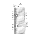
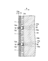
- FIG. 2 is a cross-sectional view showing the structure around the light emitting element and the mounting substrate according to the first embodiment of the present invention shown in FIG. It is the expanded sectional view which showed the structure of the screw and reflector of 1st Embodiment of this invention shown in FIG. It is sectional drawing which showed the light emitting element and mounting substrate periphery structure of 2nd Embodiment of this invention from the display panel side. It is the expanded sectional view which showed the structure of the screw, reflector, and elastic member of 2nd Embodiment of this invention shown in FIG.
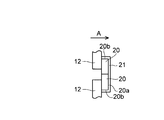
- FIG. 10 is an enlarged cross-sectional view illustrating a structure around a connector member according to a fifth embodiment of the present invention illustrated in FIG. 9.
- FIG. 14 is a cross-sectional view showing a structure around a light emitting element and a mounting substrate of the conventional display device shown in FIG. 13 from the display panel side.
- the display device 1 is used in, for example, a television receiver.
- the display device 1 includes a display panel 2 (illuminated member) and a lighting device 10 that is disposed on the back side of the display panel 2 and illuminates the display panel 2.
- the “back side (lower side in FIG. 1)” of the “back side of the display panel 2” is an orientation concept that is also applied to other components.
- the display panel 2 is composed of a liquid crystal display panel, and has two glass substrates that sandwich a liquid crystal layer (not shown).
- the display panel 2 displays an image by being illuminated by the illumination device 10.
- the lighting device 10 is an edge light type (also referred to as a side light type) backlight device.
- the lighting device 10 includes a plurality of light emitting elements 11, a mounting substrate 12 on which the plurality of light emitting elements 11 are mounted, a metal heat dissipating member (support member) 13 to which the mounting substrate 12 is attached, and the light emitting elements 11.
- the light guide plate 14 that guides the light and the metal chassis 15 that houses them are included.
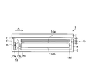
- the plurality of light emitting elements 11 are disposed to face the light incident side surface 14 c of the light guide plate 14. In other words, the plurality of light emitting elements 11 are arranged along one side of the light guide plate 14.
- the light emitting element 11 emits light in the A direction toward the light guide plate 14.
- the light emitting element 11 is composed of an LED, for example, and emits white light.
- the direction A is an example of the “predetermined direction” in the present invention.
- the light guide plate 14 is formed in a flat plate shape as shown in FIG.
- the light guide plate 14 is the widest surface and emits planar light toward the display panel 2, a back surface 14 b provided on the side opposite to the light output surface 14 a, It has a light incident side surface 14c on which light is incident and three side surfaces 14d.
- the light guide plate 14 has a function of guiding light incident on the light incident side surface 14c and emitting planar light toward the display panel 2 by changing the traveling direction of the light.
- the mounting substrate 12 is formed with a plurality of through holes 12a into which screws 16 (attachment members) are inserted.
- the through hole 12a is formed between regions of the mounting substrate 12 where the light emitting elements 11 are mounted.
- the heat dissipation member 13 is formed by bending a metal plate and has an L-shaped cross section.
- the heat radiating member 13 includes an attachment portion 13 a to which the mounting substrate 12 is attached, and a fixing portion 13 b that is connected to the attachment portion 13 a and is fixed to the chassis 15.
- the fixing portion 13b is fixed to the chassis 15 using a fixing member such as a screw (not shown).
- a plurality of screw holes 13 c to which screws 16 are attached are formed in the attachment portion 13 a of the heat radiating member 13.
- the screw hole 13 c is formed at a position corresponding to the through hole 12 a of the mounting substrate 12.
- the mounting substrate 12 is attached to the heat radiating member 13 using screws 16.
- a reflector 17 (first reflector) is provided on the light guide plate 14 side (A direction side) of the screw 16.
- the screw head 16a (protruding portion) of the screw 16 is disposed so as to protrude from the mounting substrate 12 toward the light guide plate 14 (A direction side).
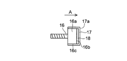
- the entire screw head 16 a of the screw 16 is covered with the reflector 17. That is, as shown in FIG. 3, the end surface (surface on the light guide plate 14 side) 16 b and the side surface 16 c of the screw head 16 a are covered with the reflector 17.
- the surface 17a of the reflector 17 on the light guide plate 14 side (A direction side) is located closer to the light guide plate 14 side (A direction side) than the light emitting element 11, as shown in FIG.
- the reflector 17 has a reflectance of about 99% or more, and has a reflectance that is twice or more that of the screw 16.
- the heat generated in the light emitting element 11 is radiated to the heat radiating member 13 and the chassis 15 through the mounting substrate 12. Thereby, it is possible to suppress that the light emitting element 11 and the light-guide plate 14 become high temperature.
- the reflector 17 so as to cover the A direction side (light guide plate 14 side) of the screw head 16a of the screw 16, the light is emitted from the light emitting element 11 and the surface of the light guide plate 14 ( Light reflected by the light incident side surface 14c) can be suppressed from being absorbed by the screw 16. That is, the light reflected by the light guide plate 14 can be reflected by the reflector 17 toward the direction A (light guide plate 14 side). Thereby, since it can suppress that the front part (part which opposes the screw head 16a in the peripheral part of the light-guide plate 14) of the screw 16 looks dark on the display panel 2 compared with another part, the display panel 2 can be suppressed. The occurrence of uneven brightness can be suppressed.
- the reflector 17 that covers the A direction side (light guide plate 14 side) of the screw head 16a (projecting portion) of the screw 16, for example, even when the light guide plate 14 is thermally expanded, the light guide plate 14 is screwed. Since direct contact with 16 can be prevented, the surface of the light guide plate 14 can be prevented from being damaged.
- the surface 17 a on the A direction side (light guide plate 14 side) of the reflector 17 is located on the A direction side (light guide plate 14 side) with respect to the light emitting element 11. Therefore, since it can prevent that the light-guide plate 14 contacts the light emitting element 11, it can prevent that the light emitting element 11 is damaged.
- the entire screw head 16 a of the screw 16 is covered with the reflector 17. Thereby, since the light is not absorbed by the screw 16, it is possible to further suppress the occurrence of luminance unevenness in the display panel 2.
- the heat generated in the light emitting element 11 can be radiated to the heat radiating member 13 and the chassis 15 through the mounting substrate 12.
- the heat dissipation can be improved.
- the mounting substrate 12 can be easily attached to the heat dissipation member 13 by using the screws 16.
- the present invention is particularly effective when the screw head 16a is disposed on the A direction side (light guide plate 14 side) with respect to the mounting substrate 12.
- an elastic member 18 is provided between the screw head 16 a of the screw 16 and the reflector 17. Specifically, as shown in FIG. 5, the elastic member 18 is disposed between the end face (surface in the A direction) 16 b of the screw head 16 a and the reflector 17.
- the elastic member 18 is made of, for example, urethane foam, sponge, rubber, or the like that is commercially available under the trade name of PORON (registered trademark).
- the elastic member 18 has a thickness of about 0.1 mm to about 1 mm, for example.
- the elastic member 18 is provided between the screw head 16a of the screw 16 and the reflector 17 as described above.
- the elastic member 18 functions as a buffer material when the light guide plate 14 contacts the reflector 17, it is possible to further suppress the surface of the light guide plate 14 from being damaged.
- the light guide plate 14 can be designed on the assumption that it contacts the reflector 17, the light guide plate 14 can be disposed close to the light emitting element 11. Thereby, the incident efficiency of the light emitted from the light emitting element 11 can be improved, and the lighting device 10 can be downsized.
- an optical sheet 19 is combined with the display device 1 of any of the first to third embodiments.
- a plurality of optical sheets 19 are arranged on the back side of the display panel 2 (between the back side of the display panel 2 and the light emission surface 14 a of the light guide plate 14).
- the plurality of optical sheets 19 includes a lens sheet on which a plurality of lenses are formed, and has a function of condensing light from the light guide plate 14 at a predetermined viewing angle.
- the plurality of optical sheets 19 include, for example, a diffusion plate and a prism sheet in addition to the lens sheet.
- the other structure of the fourth embodiment is the same as that of the first to third embodiments.
- the lens sheet (optical sheet 19) is disposed on the back side of the display panel 2.
- the lens sheet (optical sheet 19) is arranged on the back side of the display panel 2, the brightness and darkness on the display panel 2 is easily visually recognized, and uneven brightness tends to occur on the display panel 2. Therefore, the present invention is particularly effective when a lens sheet (optical sheet 19) is disposed on the back side of the display panel 2.
- the connector member 20 is attached to the mounting substrate 12.
- the connector member 20 is provided to electrically connect adjacent mounting boards 12 or to electrically connect the mounting board 12 and an external component (not shown).
- a reflector 21 (second reflector) is provided on the light guide plate 14 side (A direction side) of the connector member 20, and the entire connector member 20 is covered with the reflector 21. That is, as shown in FIG. 10, the end surface (surface on the A direction side) 20 a and the side surface 20 b of the connector member 20 are covered with the reflector 21.
- the reflector 21 may be formed so as not to cover the side surface 20b of the connector member 20. Further, the reflector 21 may be formed of the same material as the reflector 17.
- the reflective sheet 17 having the same structure as that of the first embodiment is illustrated, but the structure of the reflective sheet 17 may be the same as that of the second or third embodiment.
- the connector member 20 is attached to the mounting substrate 12, and the reflector 21 is provided so as to cover the A direction side of the connector member 20. Thereby, it is possible to suppress the light emitted from the light emitting element 11 and reflected by the surface of the light guide plate 14 from being absorbed by the connector member 20. Thereby, it is possible to further suppress the occurrence of luminance unevenness in the display panel 2.
- the illumination device 110 includes a plurality of light emitting elements 11, a mounting substrate 12, and the back side of the display panel 2 (between the display panel 2 and the light emitting elements 11. ) And a plurality of optical sheets 19 and a metal chassis 115 (support member, heat radiating member) for housing them.
- the chassis 115 has a plurality of screw holes 115a to which the screws 16 are attached.
- the through hole 115 a is formed at a position corresponding to the screw hole 12 a of the mounting substrate 12.
- the mounting board 12 is attached to the chassis 115 using screws 16.
- the light emitting element 11 emits light in the A1 direction toward the diffusion plate 111.
- a reflector 17 is provided on the diffusion plate 111 side (A1 direction side) of the screw 16.
- the screw head 16 a (protruding portion) of the screw 16 is disposed on the diffusion plate 111 (A1 direction side) with respect to the mounting substrate 12.
- the entire screw head 16 a of the screw 16 is covered with the reflector 17.
- the A1 direction is an example of the “predetermined direction” in the present invention.
- the heat generated in the light emitting element 11 is radiated to the chassis 115 via the mounting substrate 12, and the chassis 115 functions as a heat radiating member.
- the reflective sheet 17 having the same structure as that of the first embodiment is illustrated, but the structure of the reflective sheet 17 may be the same as that of the second or third embodiment.
- the other structure of the sixth embodiment is the same as that of the first to fifth embodiments.
- the reflector 17 on the A1 direction side (the diffusion plate 111 side) of the screw head 16a of the screw 16, the light is emitted from the light emitting element 11 and reflected by the surface of the diffusion plate 111. It is possible to prevent light from being absorbed by the screw 16. That is, the light reflected by the diffusion plate 111 can be reflected by the reflector 17 toward the A1 direction. Thereby, it can suppress that the front part (part just above the screw 16, the part which opposes the screw head 16a of the diffusion plate 111) of the screw
- the reflector 17 on the A1 direction side of the screw 16, it is possible to prevent the diffuser plate 111 from coming into direct contact with the screw 16, and thus it is possible to suppress the surface of the diffuser plate 111 from being damaged.
- the heat generated in the light emitting element 11 can be dissipated to the chassis 115 via the mounting substrate 12, so that the heat dissipation of the lighting device 110 can be improved.
- the present invention is not limited thereto, and may be applied to a display panel other than the liquid crystal display panel.
- the backlight apparatus which illuminates a display panel was demonstrated as an example of an illuminating device, this invention is applicable not only to this but the illuminating device which illuminates to-be-illuminated members other than a display panel. is there.
- the screw is used as the mounting member for mounting the mounting substrate to the support member.
- the present invention is not limited to this.
- rivets, clips, or other members may be used as the attachment member.
- an optical sheet such as a lens sheet is provided on the back side of the display panel when the lighting device is a direct backlight device.
- the present invention is not limited thereto. Absent. Since the optical sheet is provided as necessary, when the lighting device is a direct type backlight device, the lens sheet may not be provided on the back side of the display panel.
- the mounting board when the lighting device is an edge light type backlight device, the mounting board is attached to the heat radiating member (support member) and the heat radiating member is fixed to the chassis.
- the present invention is not limited to this.
- the mounting substrate may be directly attached to the chassis, and the chassis may function as a heat radiating member, as in the sixth embodiment.
- the mounting substrate when the lighting device is a direct-type backlight device, the mounting substrate may be attached to the heat dissipation member (support member) and the heat dissipation member may be fixed to the chassis.
- the present invention is not limited to this. You may arrange
- the description has been made by omitting the reflective sheet that is normally disposed inside the chassis, but it is preferable to provide the reflective sheet inside the chassis. If comprised in this way, the utilization efficiency of light can be improved easily.
- Display device 1 Display panel (illuminated member) DESCRIPTION OF SYMBOLS 10,110 Illuminating device 11
- Light emitting element 12 Mounting board 13
- Light guide plate 16 Screw (mounting member) 16a Screw head (protrusion) 17
- Reflector (first reflector) 17a surface (surface on the predetermined direction side of the first reflector) 18
- Elastic member 19 Optical sheet (lens sheet) 20
- Connector member 21 Reflector (second reflector) 115 Chassis (support member, heat dissipation member)
Landscapes
- Physics & Mathematics (AREA)
- General Physics & Mathematics (AREA)
- Optics & Photonics (AREA)
- Planar Illumination Modules (AREA)
Abstract
被照明部材の輝度ムラを抑制することが可能な照明装置を提供する。この照明装置(10)は、A方向に光を出射する複数の発光素子(11)と、複数の発光素子が実装される実装基板(12)と、実装基板が取り付けられる放熱部材(13)と、実装基板を放熱部材に取り付けるためのネジ(16)と、を備える。ネジのネジ頭(16a)のA方向側を覆うように反射体(17)が設けられている。
Description
この発明は、照明装置およびそれを備えた表示装置に関し、特に、発光素子が実装される実装基板を含む照明装置およびそれを備えた表示装置に関する。
液晶表示装置(表示装置)は、表示パネル(被照明部材)が非発光型なので、通常、表示パネルに対して光を照射するバックライト装置(照明装置)が搭載される。このようなバックライト装置として、複数のLED(発光素子)と、LEDが実装される実装基板とを備えたバックライト装置が知られている。
図13および図14は、発光素子および実装基板を備えた従来の表示装置の一例の構造を示した断面図である。表示装置1001は図13に示すように、液晶パネル(被照明部材)1002と、液晶パネル1002を照明するバックライト装置(照明装置)1010とを備えている。バックライト装置1010は、複数のLED(発光素子)1011と、複数のLED1011が実装された実装基板1012と、実装基板1012が取り付けられる支持部材1013と、LED1011からの光が入射される導光板1014と、これらを収納するシャーシ1015とを含んでいる。
導光板1014は、最も広い面であるとともに液晶パネル1002側に設けられた光出射面1014aと、光出射面1014aに対して交差して設けられるとともにLED1011からの光が入射される光入射側面1014bとを有する。
実装基板1012は図14に示すように、複数のネジ1050を用いて支持部材1013に固定されている。ネジ1050はLED1011同士の間に配置されている。ネジ1050のネジ頭1050aは実装基板1012よりも導光板1014側に配置されている。ネジ頭1050aの導光板1014側の面は、LED1011よりも導光板1014側に位置している。すなわち、ネジ頭1050aはLED1011よりも導光板1014側に突出している。これにより、導光板1014がLED1011に接触するのを防止し、LED1011が損傷するのを防止することが可能である。
なお、LED(発光素子)同士の間にネジが設けられた表示装置は、例えば特許文献1に開示されている。上記特許文献1では、発光素子が実装された実装基板が、ネジを用いて導光板に固定されている。この構造では、導光板中を進行する光の一部がネジにより吸収されてしまい、光の利用効率が低下する。このため、実装基板と導光板とを分離することが好ましい。導光板から分離した実装基板は支持部材に固定する必要があり、その固定に用いられるネジのネジ頭を、導光板の移動を規制するストッパとして利用したのが図13および図14に示した従来の表示装置1001の特徴である。
しかしながら、従来の表示装置1001では、ネジ1050が導光板1014側に露出しているので、LED1011から出射し導光板1014の表面(光入射側面1014b)で反射された光の一部は、ネジ1050で吸収される。このため、ネジ1050の正面部分(導光板1014の周縁部においてネジ頭1050aに対向する部分)が他の部分に比べて画面(被照明部材)上で暗く見えるので、画面に輝度ムラが発生するという問題点がある。
この発明は、上記のような課題を解決するためになされたものであり、この発明の目的は、被照明部材の輝度ムラを抑制することが可能な照明装置およびそれを備えた表示装置を提供することである。
上記目的を達成するために、この発明の照明装置は、被照明部材を照明する照明装置であって、所定方向に光を出射する複数の発光素子と、複数の発光素子が実装される実装基板と、実装基板が取り付けられる支持部材と、実装基板を支持部材に取り付けるための取付部材と、を備え、取付部材は実装基板よりも前記所定方向側に突出する突出部を含み、突出部の前記所定方向側を覆うように第1反射体が設けられている。
この照明装置では、上記のように、取付部材の突出部の前記所定方向側を覆うように第1反射体を設けることによって、発光素子から出射し導光板や拡散板などの表面で反射された光が取付部材で吸収されるのを抑制することができる。すなわち、導光板や拡散板などで反射された光を、第1反射体により前記所定方向側に反射させることができる。これにより、取付部材の正面部分が他の部分に比べて被照明部材上で暗く見えるのを抑制することができるので、被照明部材に輝度ムラが発生するのを抑制することができる。
また、取付部材の突出部の前記所定方向側に第1反射体を設けることによって、導光板や拡散板などが取付部材に直接接触するのを防止することができるので、導光板や拡散板などの表面が傷つくのを抑制することができる。
上記照明装置において、好ましくは、第1反射体の前記所定方向側の面は、発光素子よりも前記所定方向側に位置している。このように構成すれば、導光板や拡散板などが発光素子に接触するのを防止することができるので、発光素子が損傷するのを防止することができる。
この場合、好ましくは、取付部材の突出部と第1反射体との間には、弾性部材が設けられている。このように構成すれば、導光板や拡散板などが第1反射体に接触した場合に弾性部材が緩衝材として機能するので、導光板や拡散板などの表面が傷つくのをより抑制することができる。さらに、導光板や拡散板などが第1反射体に接触することを前提として設計することが可能となるので、導光板や拡散板などを発光素子に近づけて配置することができる。これにより、発光素子から出射した光の入光効率を向上させることができるとともに、照明装置を小型化することができる。
上記照明装置において、好ましくは、取付部材の突出部全体が、第1反射体により覆われている。このように構成すれば、取付部材で光が吸収されることがないので、被照明部材に輝度ムラが発生するのをより抑制することができる。
上記照明装置において、好ましくは、発光素子から出射した光が入射される導光板をさらに備える。
上記照明装置において、好ましくは、支持部材は金属製の放熱部材を含む。このように構成すれば、発光素子で発生した熱を実装基板を介して放熱部材に放熱させることができるので、照明装置の放熱性を向上させることができる。
上記照明装置において、好ましくは、取付部材はネジからなる。このように構成すれば、実装基板を容易に支持部材に取り付けることができる。
上記取付部材がネジからなる照明装置において、ネジのネジ頭が実装基板よりも前記所定方向側に配置されている場合、その部分(ネジ頭が配置されている部分)での発光素子の配置間隔が大きくなり、被照明部材に輝度ムラが発生しやすくなる。また、ネジのネジ頭が実装基板よりも前記所定方向側に配置されている場合、光を吸収する面積(ネジの実装基板よりも前記所定方向側に配置されている部分の面積)が大きくなるので、被照明部材に輝度ムラが発生しやすくなる。このため、ネジ頭が実装基板よりも前記所定方向側に配置されている場合に、本発明は特に有効である。
上記照明装置において、被照明部材の背面側にレンズシートを配置した場合に、被照明部材上の明暗が視認されやすくなり、被照明部材に輝度ムラが発生しやすくなる。このため、被照明部材の背面側にレンズシートが配置されている場合に、本発明は特に有効である。
上記照明装置において、好ましくは、実装基板にはコネクタ部材が取り付けられており、コネクタ部材の前記所定方向側を覆うように第2反射体が設けられている。このように構成すれば、発光素子から出射し導光板や拡散板などの表面で反射された光がコネクタ部材で吸収されるのを抑制することができる。これにより、被照明部材に輝度ムラが発生するのをより抑制することができる。
この発明の表示装置は、上記の構成の照明装置と、照明装置に照明される表示パネルとを備える。このように構成すれば、被照明部材の輝度ムラを抑制することが可能な表示装置を得ることができる。
以上のように、本発明によれば、被照明部材の輝度ムラを抑制することが可能な照明装置およびそれを備えた表示装置を容易に得ることができる。
以下、本発明の実施形態について図面を参照して説明する。なお、理解を容易にするために、断面図であってもハッチングを施さない場合がある。
(第1実施形態)
図1~図3を参照して、本発明の第1実施形態による表示装置1の構造について説明する。
図1~図3を参照して、本発明の第1実施形態による表示装置1の構造について説明する。
本発明の第1実施形態による表示装置1は例えばテレビジョン受像機などに用いられるものである。また、表示装置1は図1に示すように、表示パネル2(被照明部材)と、表示パネル2の背面側に配置され、表示パネル2を照明する照明装置10とを備えている。なお、「表示パネル2の背面側」の「背面側(図1では下側)」は、他の構成要素にも適用される方位概念である。
表示パネル2は液晶表示パネルからなり、図示しない液晶層を挟み込む2枚のガラス基板を有する。また、表示パネル2は照明装置10に照明されることにより画像を表示する。
照明装置10はエッジライト型(サイドライト型とも言う)のバックライト装置である。また、照明装置10は、複数の発光素子11と、複数の発光素子11が実装された実装基板12と、実装基板12が取り付けられる金属製の放熱部材(支持部材)13と、発光素子11からの光を導く導光板14と、これらを収納する金属製のシャーシ15とを含んでいる。
複数の発光素子11は図2に示すように、導光板14の光入射側面14cに対向配置されている。言い換えると、複数の発光素子11は導光板14の1辺に沿って配置されている。発光素子11は導光板14に向かってA方向に光を出射する。発光素子11は例えばLEDにより構成されており、白色光を出射する。なお、A方向は、本発明の「所定方向」の一例である。
導光板14は図1に示すように、平板状に形成されている。導光板14は、最も広い面であるとともに表示パネル2に向かって面状光を出射する光出射面14aと、光出射面14aとは反対側に設けられた背面14bと、発光素子11からの光が入射される光入射側面14cと、3つの側面14dとを有する。導光板14は、光入射側面14cに入射した光を導光し、光の進行方向を変更して表示パネル2に向かって面状光を出射する機能を有する。
導光板14の背面14bには、光入射側面14cに入射した光の進行方向を変更して、光を光出射面14aから表示パネル2側に出射させる多数の散乱ドットなど(図示せず)が形成されている。
実装基板12には図2に示すように、ネジ16(取付部材)が挿入される複数の貫通穴12aが形成されている。また、貫通穴12aは実装基板12の発光素子11が搭載される領域同士の間に形成されている。
放熱部材13は図1に示すように、金属板を折り曲げることにより形成されており、L字状の断面を有する。放熱部材13は、実装基板12が取り付けられる取付部13aと、取付部13aに繋がるとともにシャーシ15に固定される固定部13bとを含んでいる。固定部13bは図示しないネジなどの固定部材を用いてシャーシ15に固定されている。
放熱部材13の取付部13aには図2に示すように、ネジ16が取り付けられる複数のネジ穴13cが形成されている。このネジ穴13cは実装基板12の貫通穴12aに対応する位置に形成されている。そして、実装基板12はネジ16を用いて放熱部材13に取り付けられている。
ここで、ネジ16の導光板14側(A方向側)には、反射体17(第1反射体)が設けられている。具体的には、ネジ16のネジ頭16a(突出部)は、実装基板12よりも導光板14側(A方向側)に突出して配置されている。そして、ネジ16のネジ頭16a全体が、反射体17により覆われている。すなわち、図3に示すように、ネジ頭16aの端面(導光板14側の面)16bおよび側面16cが、反射体17により覆われている。
反射体17の導光板14側(A方向側)の面17aは図2に示すように、発光素子11よりも導光板14側(A方向側)に位置している。なお、反射体17は約99%以上の反射率を有しており、ネジ16の反射率の2倍以上の反射率を有する。
この表示装置1では、発光素子11で発生した熱は実装基板12を介して放熱部材13やシャーシ15に放熱される。これにより、発光素子11や導光板14が高温になるのを抑制することが可能である。
本実施形態では、上記のように、ネジ16のネジ頭16aのA方向側(導光板14側)を覆うように反射体17を設けることによって、発光素子11から出射し導光板14の表面(光入射側面14c)で反射された光がネジ16で吸収されるのを抑制することができる。すなわち、導光板14で反射された光を、反射体17によりA方向側(導光板14側)に反射させることができる。これにより、ネジ16の正面部分(導光板14の周縁部においてネジ頭16aに対向する部分)が他の部分に比べて表示パネル2上で暗く見えるのを抑制することができるので、表示パネル2に輝度ムラが発生するのを抑制することができる。
また、ネジ16のネジ頭16a(突出部)のA方向側(導光板14側)を覆う反射体17を設けることによって、例えば導光板14が熱膨張した場合であっても導光板14がネジ16に直接接触するのを防止することができるので、導光板14の表面が傷つくのを抑制することができる。
また、上記のように、反射体17のA方向側(導光板14側)の面17aは、発光素子11よりもA方向側(導光板14側)に位置している。これにより、導光板14が発光素子11に接触するのを防止することができるので、発光素子11が損傷するのを防止することができる。
また、上記のように、ネジ16のネジ頭16a全体が、反射体17により覆われている。これにより、ネジ16で光が吸収されることがないので、表示パネル2に輝度ムラが発生するのをより抑制することができる。
また、上記のように、金属製の放熱部材13を設けることによって、発光素子11で発生した熱を実装基板12を介して放熱部材13およびシャーシ15に放熱させることができるので、照明装置10の放熱性を向上させることができる。
また、上記のように、ネジ16を用いることによって、実装基板12を容易に放熱部材13に取り付けることができる。
また、上記のように、ネジ16のネジ頭16aが実装基板12よりもA方向側(導光板14側)に配置されている場合に、その部分(ネジ頭16aが配置されている部分)での発光素子11の配置間隔が大きくなり、表示パネル2に輝度ムラが発生しやすくなる。また、ネジ16のネジ頭16aが実装基板12よりもA方向側に配置されている場合に、光を吸収する面積(ネジ16の実装基板12よりもA方向側に配置されている部分の面積)が大きくなるので、表示パネル2に輝度ムラが発生しやすくなる。このため、ネジ頭16aが実装基板12よりもA方向側(導光板14側)に配置されている場合に、本発明は特に有効である。
(第2実施形態)
本発明の第2実施形態の表示装置では図4に示すように、ネジ16のネジ頭16aと反射体17との間には、弾性部材18が設けられている。具体的には図5に示すように、弾性部材18はネジ頭16aの端面(A方向側の面)16bと反射体17との間に配置されている。弾性部材18は例えばポロン(登録商標)という商品名で市販されているウレタンフォーム、スポンジまたはゴムなどにより形成されている。弾性部材18は例えば約0.1mm~約1mmの厚みを有する。
本発明の第2実施形態の表示装置では図4に示すように、ネジ16のネジ頭16aと反射体17との間には、弾性部材18が設けられている。具体的には図5に示すように、弾性部材18はネジ頭16aの端面(A方向側の面)16bと反射体17との間に配置されている。弾性部材18は例えばポロン(登録商標)という商品名で市販されているウレタンフォーム、スポンジまたはゴムなどにより形成されている。弾性部材18は例えば約0.1mm~約1mmの厚みを有する。
第2実施形態のその他の構造は、上記第1実施形態と同様である。
本実施形態では、上記のように、ネジ16のネジ頭16aと反射体17との間には、弾性部材18が設けられている。これにより、導光板14が反射体17に接触した場合に弾性部材18が緩衝材として機能するので、導光板14の表面が傷つくのをより抑制することができる。さらに、導光板14が反射体17に接触することを前提として設計することが可能となるので、導光板14を発光素子11に近づけて配置することができる。これにより、発光素子11から出射した光の入光効率を向上させることができるとともに、照明装置10を小型化することができる。
第2実施形態のその他の効果は、上記第1実施形態と同様である。
(第3実施形態)
本発明の第3実施形態の表示装置では図6および図7に示すように、ネジ16のネジ頭16aの端面16bは反射体17により覆われており、ネジ頭16aの側面16cは反射体17により覆われていない。また、ネジ16のネジ頭16aと反射体17との間には、弾性部材18が設けられている。なお、上記第1実施形態と同様に弾性部材18が設けられていなくてもよい。
本発明の第3実施形態の表示装置では図6および図7に示すように、ネジ16のネジ頭16aの端面16bは反射体17により覆われており、ネジ頭16aの側面16cは反射体17により覆われていない。また、ネジ16のネジ頭16aと反射体17との間には、弾性部材18が設けられている。なお、上記第1実施形態と同様に弾性部材18が設けられていなくてもよい。
第3実施形態のその他の構造および効果は、上記第1および第2実施形態と同様である。
(第4実施形態)
本発明の第4実施形態は、上記第1~第3実施形態のいずれかの表示装置1に光学シート19を組み合わせたものである。第4実施形態の表示装置では図8に示すように、表示パネル2の背面側(表示パネル2の背面と導光板14の光出射面14aとの間)に複数の光学シート19が配置されている。複数の光学シート19は複数のレンズが形成されたレンズシートを含んでおり、導光板14からの光を所定の視野角に集光する機能を有する。なお、複数の光学シート19はレンズシート以外に、例えば拡散板およびプリズムシートなどを含んでいる。
本発明の第4実施形態は、上記第1~第3実施形態のいずれかの表示装置1に光学シート19を組み合わせたものである。第4実施形態の表示装置では図8に示すように、表示パネル2の背面側(表示パネル2の背面と導光板14の光出射面14aとの間)に複数の光学シート19が配置されている。複数の光学シート19は複数のレンズが形成されたレンズシートを含んでおり、導光板14からの光を所定の視野角に集光する機能を有する。なお、複数の光学シート19はレンズシート以外に、例えば拡散板およびプリズムシートなどを含んでいる。
第4実施形態のその他の構造は、上記第1~第3実施形態と同様である。
本実施形態では、上記のように、表示パネル2の背面側にレンズシート(光学シート19)を配置している。表示パネル2の背面側にレンズシート(光学シート19)を配置した場合、表示パネル2上の明暗が視認されやすくなり、表示パネル2に輝度ムラが発生しやすくなる。このため、表示パネル2の背面側にレンズシート(光学シート19)を配置している場合に、本発明は特に有効である。
第4実施形態のその他の効果は、上記第1~第3実施形態と同様である。
(第5実施形態)
本発明の第5実施形態の表示装置では図9に示すように、実装基板12にコネクタ部材20が取り付けられている。このコネクタ部材20は、隣接する実装基板12同士を電気的に接続したり、実装基板12と外部部品(図示せず)とを電気的に接続するために設けられている。
本発明の第5実施形態の表示装置では図9に示すように、実装基板12にコネクタ部材20が取り付けられている。このコネクタ部材20は、隣接する実装基板12同士を電気的に接続したり、実装基板12と外部部品(図示せず)とを電気的に接続するために設けられている。
コネクタ部材20の導光板14側(A方向側)には反射体21(第2反射体)が設けられており、コネクタ部材20全体が反射体21により覆われている。すなわち、図10に示すように、コネクタ部材20の端面(A方向側の面)20aおよび側面20bが、反射体21により覆われている。なお、反射体21は、コネクタ部材20の側面20bを覆わないように形成されていてもよい。また、反射体21は反射体17と同じ材料により形成されていてもよい。
第5実施形態では、反射シート17として第1実施形態と同じ構造のものが図示されているが、反射シート17の構造は上記第2または第3実施形態と同じであってもよい。
第5実施形態のその他の構造は、上記第1~第4実施形態と同様である。
本実施形態では、上記のように、実装基板12にコネクタ部材20が取り付けられているとともに、コネクタ部材20のA方向側を覆うように反射体21が設けられている。これにより、発光素子11から出射し導光板14の表面で反射された光がコネクタ部材20で吸収されるのを抑制することができる。これにより、表示パネル2に輝度ムラが発生するのをより抑制することができる。
第5実施形態のその他の効果は、上記第1~第4実施形態と同様である。
(第6実施形態)
この第6施形態では図11および図12を参照して、上記第1~第5実施形態とは異なり、照明装置110が直下型のバックライト装置である場合について説明する。
この第6施形態では図11および図12を参照して、上記第1~第5実施形態とは異なり、照明装置110が直下型のバックライト装置である場合について説明する。
第6実施形態の表示装置101では図11に示すように、照明装置110は、複数の発光素子11と、実装基板12と、表示パネル2の背面側(表示パネル2と発光素子11との間)に配置される拡散板111および複数の光学シート19と、これらを収納する金属製のシャーシ115(支持部材、放熱部材)とを含んでいる。
シャーシ115には図12に示すように、ネジ16が取り付けられる複数のネジ穴115aが形成されている。この貫通穴115aは実装基板12のネジ穴12aに対応する位置に形成されている。そして、ネジ16を用いて、実装基板12がシャーシ115に取り付けられている。
本実施形態では、発光素子11は拡散板111に向かってA1方向に光を出射する。ネジ16の拡散板111側(A1方向側)には、反射体17が設けられている。具体的には、ネジ16のネジ頭16a(突出部)は、実装基板12よりも拡散板111(A1方向側)に配置されている。そして、ネジ16のネジ頭16a全体が、反射体17により覆われている。なお、A1方向は、本発明の「所定方向」の一例である。
この表示装置101では、発光素子11で発生した熱は実装基板12を介してシャーシ115に放熱され、シャーシ115が放熱部材として機能する。
第6実施形態では、反射シート17として第1実施形態と同じ構造のものが図示されているが、反射シート17の構造は上記第2または第3実施形態と同じであってもよい。
第6実施形態のその他の構造は、上記第1~第5実施形態と同様である。
本実施形態では、上記のように、ネジ16のネジ頭16aのA1方向側(拡散板111側)に反射体17を設けることによって、発光素子11から出射し拡散板111の表面で反射された光がネジ16で吸収されるのを防止することができる。すなわち、拡散板111で反射された光を、反射体17によりA1方向側に反射させることができる。これにより、ネジ16の正面部分(ネジ16の真上の部分、拡散板111のネジ頭16aに対向する部分)が他の部分に比べて表示パネル2上で暗く見えるのを抑制することができるので、表示パネル2に輝度ムラが発生するのを抑制することができる。
また、ネジ16のA1方向側に反射体17を設けることによって、拡散板111がネジ16に直接接触するのを防止することができるので、拡散板111の表面が傷つくのを抑制することができる。
また、上記のように、発光素子11で発生した熱を実装基板12を介してシャーシ115に放熱させることができるので、照明装置110の放熱性を向上させることができる。
第6実施形態のその他の効果は、上記第1~第5実施形態と同様である。
なお、今回開示された実施形態は、すべての点で例示であって制限的なものではないと考えられるべきである。本発明の範囲は、上記した実施形態の説明ではなく請求の範囲によって示され、さらに請求の範囲と均等の意味および範囲内でのすべての変更が含まれる。
例えば、上記実施形態では、表示パネルを液晶表示パネルに適用した例について示したが、本発明はこれに限らず、液晶表示パネル以外の表示パネルに適用してもよい。
また、上記実施形態では、照明装置の一例として表示パネルを照明するバックライト装置について説明したが、本発明はこれに限らず、表示パネル以外の被照明部材を照明する照明装置にも適用可能である。
また、上記実施形態では、実装基板を支持部材に取り付けるための取付部材としてネジを用いた例について説明したが、本発明はこれに限らない。取付部材として、例えばリベット、クリップやその他の部材を用いてもよい。
また、上記実施形態では、複数の発光素子を導光板の1辺に沿って配置させる例について示したが、本発明はこれに限らず、複数の発光素子を導光板の2辺または4辺に沿って配置させてもよい。
また、上記第6実施形態では、照明装置が直下型のバックライト装置である場合に、表示パネルの背面側にレンズシートなどの光学シートを設けた例について示したが、本発明はこれに限らない。光学シートは必要に応じて設けられるものであるので、照明装置が直下型のバックライト装置である場合に、表示パネルの背面側にレンズシートを設けなくてもよい。
また、上記第1~第5実施形態では、照明装置がエッジライト型のバックライト装置である場合に、実装基板を放熱部材(支持部材)に取り付け、放熱部材をシャーシに固定した例について示したが、本発明はこれに限らない。照明装置がエッジライト型のバックライト装置である場合に、上記第6実施形態と同様、実装基板を直接シャーシに取り付け、シャーシを放熱部材として機能させてもよい。逆に、照明装置が直下型のバックライト装置である場合に、実装基板を放熱部材(支持部材)に取り付け、放熱部材をシャーシに固定しても当然よい。
また、上記実施形態では、ネジのネジ頭を実装基板よりも導光板(または拡散板)側に配置した例について説明したが、本発明はこれに限らない。ネジのネジ頭を実装基板よりも導光板(または拡散板)とは反対側に配置してもよい。すなわち、ネジを支持部材側から実装基板に取り付け、ネジ頭を支持部材側に露出させてもよい。
また、上記実施形態では、シャーシの内側に通常配置される反射シートを省略して説明したが、シャーシの内側に反射シートを設けることが好ましい。このように構成すれば、光の利用効率を容易に向上させることができる。
また、上述した実施形態および変形例の構成を適宜組み合わせて得られる構成についても、本発明の技術的範囲に含まれる。
1、101 表示装置
2 表示パネル(被照明部材)
10、110 照明装置
11 発光素子
12 実装基板
13 放熱部材(支持部材)
14 導光板
16 ネジ(取付部材)
16a ネジ頭(突出部)
17 反射体(第1反射体)
17a 面(第1反射体の所定方向側の面)
18 弾性部材
19 光学シート(レンズシート)
20 コネクタ部材
21 反射体(第2反射体)
115 シャーシ(支持部材、放熱部材)
2 表示パネル(被照明部材)
10、110 照明装置
11 発光素子
12 実装基板
13 放熱部材(支持部材)
14 導光板
16 ネジ(取付部材)
16a ネジ頭(突出部)
17 反射体(第1反射体)
17a 面(第1反射体の所定方向側の面)
18 弾性部材
19 光学シート(レンズシート)
20 コネクタ部材
21 反射体(第2反射体)
115 シャーシ(支持部材、放熱部材)
Claims (11)
- 被照明部材を照明する照明装置であって、
所定方向に光を出射する複数の発光素子と、
前記複数の発光素子が実装される実装基板と、
前記実装基板が取り付けられる支持部材と、
前記実装基板を前記支持部材に取り付けるための取付部材と、
を備え、
前記取付部材は前記実装基板よりも前記所定方向側に突出する突出部を含み、
前記突出部の前記所定方向側を覆うように第1反射体が設けられていることを特徴とする照明装置。 - 前記第1反射体の前記所定方向側の面は、前記発光素子よりも前記所定方向側に位置していることを特徴とする請求項1に記載の照明装置。
- 前記取付部材の突出部と前記第1反射体との間には、弾性部材が設けられていることを特徴とする請求項2に記載の照明装置。
- 前記取付部材の突出部全体が、前記第1反射体により覆われていることを特徴とする請求項1~3のいずれか1項に記載の照明装置。
- 前記発光素子から出射した光が入射される導光板をさらに備えることを特徴とする請求項1~4のいずれか1項に記載の照明装置。
- 前記支持部材は金属製の放熱部材を含むことを特徴とする請求項1~5のいずれか1項に記載の照明装置。
- 前記取付部材はネジからなることを特徴とする請求項1~6のいずれか1項に記載の照明装置。
- 前記ネジのネジ頭は、前記実装基板よりも前記所定方向側に配置されていることを特徴とする請求項7に記載の照明装置。
- 前記被照明部材の背面側に配置されるレンズシートをさらに備えることを特徴とする請求項1~8のいずれか1項に記載の照明装置。
- 前記実装基板にはコネクタ部材が取り付けられており、
前記コネクタ部材の前記所定方向側を覆うように第2反射体が設けられていることを特徴とする請求項1~9のいずれか1項に記載の照明装置。 - 請求項1~10のいずれか1項に記載の照明装置と、
前記照明装置に照明される表示パネルとを備えることを特徴とする表示装置。
Applications Claiming Priority (2)
| Application Number | Priority Date | Filing Date | Title |
|---|---|---|---|
| JP2011245469 | 2011-11-09 | ||
| JP2011-245469 | 2011-11-09 |
Publications (1)
| Publication Number | Publication Date |
|---|---|
| WO2013069552A1 true WO2013069552A1 (ja) | 2013-05-16 |
Family
ID=48289928
Family Applications (1)
| Application Number | Title | Priority Date | Filing Date |
|---|---|---|---|
| PCT/JP2012/078419 Ceased WO2013069552A1 (ja) | 2011-11-09 | 2012-11-02 | 照明装置およびそれを備えた表示装置 |
Country Status (1)
| Country | Link |
|---|---|
| WO (1) | WO2013069552A1 (ja) |
Cited By (5)
| Publication number | Priority date | Publication date | Assignee | Title |
|---|---|---|---|---|
| WO2016009543A1 (ja) * | 2014-07-17 | 2016-01-21 | 堺ディスプレイプロダクト株式会社 | 表示装置 |
| JP2020096738A (ja) * | 2018-12-18 | 2020-06-25 | サミー株式会社 | 遊技機 |
| JP2020096739A (ja) * | 2018-12-18 | 2020-06-25 | サミー株式会社 | 遊技機 |
| JP2020096735A (ja) * | 2018-12-18 | 2020-06-25 | サミー株式会社 | 遊技機 |
| JP2020096740A (ja) * | 2018-12-18 | 2020-06-25 | サミー株式会社 | 遊技機 |
Citations (3)
| Publication number | Priority date | Publication date | Assignee | Title |
|---|---|---|---|---|
| WO2011086760A1 (ja) * | 2010-01-12 | 2011-07-21 | シャープ株式会社 | Led基板、バックライトユニットおよび液晶表示装置 |
| WO2011096246A1 (ja) * | 2010-02-02 | 2011-08-11 | シャープ株式会社 | 照明装置、表示装置、及びテレビ受信装置 |
| WO2011132462A1 (ja) * | 2010-04-21 | 2011-10-27 | シャープ株式会社 | 照明装置、表示装置、及びテレビ受信装置 |
-
2012
- 2012-11-02 WO PCT/JP2012/078419 patent/WO2013069552A1/ja not_active Ceased
Patent Citations (3)
| Publication number | Priority date | Publication date | Assignee | Title |
|---|---|---|---|---|
| WO2011086760A1 (ja) * | 2010-01-12 | 2011-07-21 | シャープ株式会社 | Led基板、バックライトユニットおよび液晶表示装置 |
| WO2011096246A1 (ja) * | 2010-02-02 | 2011-08-11 | シャープ株式会社 | 照明装置、表示装置、及びテレビ受信装置 |
| WO2011132462A1 (ja) * | 2010-04-21 | 2011-10-27 | シャープ株式会社 | 照明装置、表示装置、及びテレビ受信装置 |
Cited By (12)
| Publication number | Priority date | Publication date | Assignee | Title |
|---|---|---|---|---|
| WO2016009543A1 (ja) * | 2014-07-17 | 2016-01-21 | 堺ディスプレイプロダクト株式会社 | 表示装置 |
| CN106462002A (zh) * | 2014-07-17 | 2017-02-22 | 堺显示器制品株式会社 | 显示装置 |
| JPWO2016009543A1 (ja) * | 2014-07-17 | 2017-05-25 | 堺ディスプレイプロダクト株式会社 | 表示装置 |
| US10302851B2 (en) | 2014-07-17 | 2019-05-28 | Sakai Display Products Corporation | Display apparatus |
| CN106462002B (zh) * | 2014-07-17 | 2019-06-18 | 堺显示器制品株式会社 | 显示装置 |
| JP2020096738A (ja) * | 2018-12-18 | 2020-06-25 | サミー株式会社 | 遊技機 |
| JP2020096739A (ja) * | 2018-12-18 | 2020-06-25 | サミー株式会社 | 遊技機 |
| JP2020096735A (ja) * | 2018-12-18 | 2020-06-25 | サミー株式会社 | 遊技機 |
| JP2020096740A (ja) * | 2018-12-18 | 2020-06-25 | サミー株式会社 | 遊技機 |
| JP2021120125A (ja) * | 2018-12-18 | 2021-08-19 | サミー株式会社 | 遊技機 |
| JP2021120126A (ja) * | 2018-12-18 | 2021-08-19 | サミー株式会社 | 遊技機 |
| JP7037068B2 (ja) | 2018-12-18 | 2022-03-16 | サミー株式会社 | 遊技機 |
Similar Documents
| Publication | Publication Date | Title |
|---|---|---|
| KR100852249B1 (ko) | 면상 광원장치 | |
| JPWO2009093583A1 (ja) | 表示装置および発光装置 | |
| CN101319759A (zh) | 发光器件、面光源装置和图像显示装置 | |
| JP5271649B2 (ja) | 液晶表示装置 | |
| JP5064602B2 (ja) | 表示装置 | |
| JP5238079B2 (ja) | 照明装置、表示装置およびテレビ受信装置 | |
| JP2004185010A (ja) | バックライトアセンブリ | |
| WO2011093119A1 (ja) | 照明装置、表示装置、テレビ受信装置 | |
| WO2010016322A1 (ja) | 照明装置およびそれを備えた液晶表示装置 | |
| WO2014208733A1 (ja) | 照明装置、表示装置、及びテレビ受信装置 | |
| WO2013069552A1 (ja) | 照明装置およびそれを備えた表示装置 | |
| WO2015012135A1 (ja) | 照明装置及び液晶表示装置 | |
| JP2013218125A (ja) | 液晶表示装置 | |
| JP5899722B2 (ja) | 面状光源装置および表示装置 | |
| WO2012102193A1 (ja) | 照明装置、表示装置、及びテレビ受信装置 | |
| JP5098778B2 (ja) | 照明装置、液晶表示装置及び電子機器 | |
| JP2014041761A (ja) | 照明装置、表示装置及びテレビ受信装置 | |
| JP2006195296A (ja) | 液晶表示装置 | |
| JP5717675B2 (ja) | 表示装置、及びテレビ受信装置 | |
| WO2011016268A1 (ja) | 表示装置 | |
| JP2010276628A (ja) | 液晶表示装置 | |
| JP2015108752A (ja) | 液晶表示装置 | |
| JP2010232050A (ja) | 液晶表示装置 | |
| KR102541393B1 (ko) | 디스플레이 장치 | |
| WO2018078699A1 (ja) | 照明装置および表示装置 |
Legal Events
| Date | Code | Title | Description |
|---|---|---|---|
| 121 | Ep: the epo has been informed by wipo that ep was designated in this application |
Ref document number: 12847404 Country of ref document: EP Kind code of ref document: A1 |
|
| NENP | Non-entry into the national phase |
Ref country code: DE |
|
| 122 | Ep: pct application non-entry in european phase |
Ref document number: 12847404 Country of ref document: EP Kind code of ref document: A1 |
|
| NENP | Non-entry into the national phase |
Ref country code: JP |