WO2013069406A1 - 表示装置および電子機器 - Google Patents
表示装置および電子機器 Download PDFInfo
- Publication number
- WO2013069406A1 WO2013069406A1 PCT/JP2012/076522 JP2012076522W WO2013069406A1 WO 2013069406 A1 WO2013069406 A1 WO 2013069406A1 JP 2012076522 W JP2012076522 W JP 2012076522W WO 2013069406 A1 WO2013069406 A1 WO 2013069406A1
- Authority
- WO
- WIPO (PCT)
- Prior art keywords
- guide plate
- light
- light guide
- display unit
- display
- Prior art date
Links
- 238000005286 illumination Methods 0.000 claims description 39
- 239000000853 adhesive Substances 0.000 claims description 37
- 230000001070 adhesive effect Effects 0.000 claims description 37
- 239000000463 material Substances 0.000 claims description 7
- 230000002093 peripheral effect Effects 0.000 claims description 5
- 125000006850 spacer group Chemical group 0.000 claims description 5
- 230000004888 barrier function Effects 0.000 description 30
- 230000004048 modification Effects 0.000 description 10
- 238000012986 modification Methods 0.000 description 10
- 239000004973 liquid crystal related substance Substances 0.000 description 9
- 238000000149 argon plasma sintering Methods 0.000 description 5
- 230000007423 decrease Effects 0.000 description 4
- 238000005516 engineering process Methods 0.000 description 4
- 238000000034 method Methods 0.000 description 4
- 238000012545 processing Methods 0.000 description 4
- 239000010409 thin film Substances 0.000 description 4
- TZCXTZWJZNENPQ-UHFFFAOYSA-L barium sulfate Chemical compound [Ba+2].[O-]S([O-])(=O)=O TZCXTZWJZNENPQ-UHFFFAOYSA-L 0.000 description 2
- 230000006866 deterioration Effects 0.000 description 2
- 238000010586 diagram Methods 0.000 description 2
- 230000000694 effects Effects 0.000 description 2
- 239000011521 glass Substances 0.000 description 2
- 239000011159 matrix material Substances 0.000 description 2
- 230000003287 optical effect Effects 0.000 description 2
- 238000005488 sandblasting Methods 0.000 description 2
- 238000000926 separation method Methods 0.000 description 2
- 239000004925 Acrylic resin Substances 0.000 description 1
- 229920000178 Acrylic resin Polymers 0.000 description 1
- XAGFODPZIPBFFR-UHFFFAOYSA-N aluminium Chemical compound [Al] XAGFODPZIPBFFR-UHFFFAOYSA-N 0.000 description 1
- 229910052782 aluminium Inorganic materials 0.000 description 1
- 239000006229 carbon black Substances 0.000 description 1
- 239000003086 colorant Substances 0.000 description 1
- 239000002131 composite material Substances 0.000 description 1
- 239000003822 epoxy resin Substances 0.000 description 1
- 238000000465 moulding Methods 0.000 description 1
- 239000003973 paint Substances 0.000 description 1
- 238000010422 painting Methods 0.000 description 1
- 238000000059 patterning Methods 0.000 description 1
- 239000012466 permeate Substances 0.000 description 1
- 229920003023 plastic Polymers 0.000 description 1
- 229920003229 poly(methyl methacrylate) Polymers 0.000 description 1
- 229920000647 polyepoxide Polymers 0.000 description 1
- 239000004926 polymethyl methacrylate Substances 0.000 description 1
- 238000007650 screen-printing Methods 0.000 description 1
- 229910052709 silver Inorganic materials 0.000 description 1
- 239000004332 silver Substances 0.000 description 1
- 238000002834 transmittance Methods 0.000 description 1
Images


Classifications
-
- H—ELECTRICITY
- H04—ELECTRIC COMMUNICATION TECHNIQUE
- H04N—PICTORIAL COMMUNICATION, e.g. TELEVISION
- H04N13/00—Stereoscopic video systems; Multi-view video systems; Details thereof
- H04N13/30—Image reproducers
-
- G—PHYSICS
- G02—OPTICS
- G02B—OPTICAL ELEMENTS, SYSTEMS OR APPARATUS
- G02B30/00—Optical systems or apparatus for producing three-dimensional [3D] effects, e.g. stereoscopic images
-
- G—PHYSICS
- G02—OPTICS
- G02B—OPTICAL ELEMENTS, SYSTEMS OR APPARATUS
- G02B30/00—Optical systems or apparatus for producing three-dimensional [3D] effects, e.g. stereoscopic images
- G02B30/20—Optical systems or apparatus for producing three-dimensional [3D] effects, e.g. stereoscopic images by providing first and second parallax images to an observer's left and right eyes
- G02B30/26—Optical systems or apparatus for producing three-dimensional [3D] effects, e.g. stereoscopic images by providing first and second parallax images to an observer's left and right eyes of the autostereoscopic type
- G02B30/27—Optical systems or apparatus for producing three-dimensional [3D] effects, e.g. stereoscopic images by providing first and second parallax images to an observer's left and right eyes of the autostereoscopic type involving lenticular arrays
-
- G—PHYSICS
- G02—OPTICS
- G02B—OPTICAL ELEMENTS, SYSTEMS OR APPARATUS
- G02B30/00—Optical systems or apparatus for producing three-dimensional [3D] effects, e.g. stereoscopic images
- G02B30/20—Optical systems or apparatus for producing three-dimensional [3D] effects, e.g. stereoscopic images by providing first and second parallax images to an observer's left and right eyes
- G02B30/26—Optical systems or apparatus for producing three-dimensional [3D] effects, e.g. stereoscopic images by providing first and second parallax images to an observer's left and right eyes of the autostereoscopic type
- G02B30/30—Optical systems or apparatus for producing three-dimensional [3D] effects, e.g. stereoscopic images by providing first and second parallax images to an observer's left and right eyes of the autostereoscopic type involving parallax barriers
-
- G—PHYSICS
- G02—OPTICS
- G02B—OPTICAL ELEMENTS, SYSTEMS OR APPARATUS
- G02B6/00—Light guides; Structural details of arrangements comprising light guides and other optical elements, e.g. couplings
- G02B6/0001—Light guides; Structural details of arrangements comprising light guides and other optical elements, e.g. couplings specially adapted for lighting devices or systems
- G02B6/0011—Light guides; Structural details of arrangements comprising light guides and other optical elements, e.g. couplings specially adapted for lighting devices or systems the light guides being planar or of plate-like form
-
- G—PHYSICS
- G02—OPTICS
- G02F—OPTICAL DEVICES OR ARRANGEMENTS FOR THE CONTROL OF LIGHT BY MODIFICATION OF THE OPTICAL PROPERTIES OF THE MEDIA OF THE ELEMENTS INVOLVED THEREIN; NON-LINEAR OPTICS; FREQUENCY-CHANGING OF LIGHT; OPTICAL LOGIC ELEMENTS; OPTICAL ANALOGUE/DIGITAL CONVERTERS
- G02F1/00—Devices or arrangements for the control of the intensity, colour, phase, polarisation or direction of light arriving from an independent light source, e.g. switching, gating or modulating; Non-linear optics
- G02F1/01—Devices or arrangements for the control of the intensity, colour, phase, polarisation or direction of light arriving from an independent light source, e.g. switching, gating or modulating; Non-linear optics for the control of the intensity, phase, polarisation or colour
- G02F1/13—Devices or arrangements for the control of the intensity, colour, phase, polarisation or direction of light arriving from an independent light source, e.g. switching, gating or modulating; Non-linear optics for the control of the intensity, phase, polarisation or colour based on liquid crystals, e.g. single liquid crystal display cells
- G02F1/133—Constructional arrangements; Operation of liquid crystal cells; Circuit arrangements
- G02F1/1333—Constructional arrangements; Manufacturing methods
- G02F1/1335—Structural association of cells with optical devices, e.g. polarisers or reflectors
-
- G—PHYSICS
- G09—EDUCATION; CRYPTOGRAPHY; DISPLAY; ADVERTISING; SEALS
- G09F—DISPLAYING; ADVERTISING; SIGNS; LABELS OR NAME-PLATES; SEALS
- G09F9/00—Indicating arrangements for variable information in which the information is built-up on a support by selection or combination of individual elements
-
- H—ELECTRICITY
- H04—ELECTRIC COMMUNICATION TECHNIQUE
- H04N—PICTORIAL COMMUNICATION, e.g. TELEVISION
- H04N13/00—Stereoscopic video systems; Multi-view video systems; Details thereof
- H04N13/30—Image reproducers
- H04N13/302—Image reproducers for viewing without the aid of special glasses, i.e. using autostereoscopic displays
- H04N13/31—Image reproducers for viewing without the aid of special glasses, i.e. using autostereoscopic displays using parallax barriers
- H04N13/312—Image reproducers for viewing without the aid of special glasses, i.e. using autostereoscopic displays using parallax barriers the parallax barriers being placed behind the display panel, e.g. between backlight and spatial light modulator [SLM]
-
- H—ELECTRICITY
- H04—ELECTRIC COMMUNICATION TECHNIQUE
- H04N—PICTORIAL COMMUNICATION, e.g. TELEVISION
- H04N13/00—Stereoscopic video systems; Multi-view video systems; Details thereof
- H04N13/30—Image reproducers
- H04N13/302—Image reproducers for viewing without the aid of special glasses, i.e. using autostereoscopic displays
- H04N13/32—Image reproducers for viewing without the aid of special glasses, i.e. using autostereoscopic displays using arrays of controllable light sources; using moving apertures or moving light sources
-
- H—ELECTRICITY
- H04—ELECTRIC COMMUNICATION TECHNIQUE
- H04N—PICTORIAL COMMUNICATION, e.g. TELEVISION
- H04N13/00—Stereoscopic video systems; Multi-view video systems; Details thereof
- H04N13/30—Image reproducers
- H04N13/356—Image reproducers having separate monoscopic and stereoscopic modes
-
- G—PHYSICS
- G02—OPTICS
- G02B—OPTICAL ELEMENTS, SYSTEMS OR APPARATUS
- G02B6/00—Light guides; Structural details of arrangements comprising light guides and other optical elements, e.g. couplings
- G02B6/0001—Light guides; Structural details of arrangements comprising light guides and other optical elements, e.g. couplings specially adapted for lighting devices or systems
- G02B6/0011—Light guides; Structural details of arrangements comprising light guides and other optical elements, e.g. couplings specially adapted for lighting devices or systems the light guides being planar or of plate-like form
- G02B6/0033—Means for improving the coupling-out of light from the light guide
- G02B6/0035—Means for improving the coupling-out of light from the light guide provided on the surface of the light guide or in the bulk of it
- G02B6/004—Scattering dots or dot-like elements, e.g. microbeads, scattering particles, nanoparticles
- G02B6/0043—Scattering dots or dot-like elements, e.g. microbeads, scattering particles, nanoparticles provided on the surface of the light guide
-
- G—PHYSICS
- G02—OPTICS
- G02F—OPTICAL DEVICES OR ARRANGEMENTS FOR THE CONTROL OF LIGHT BY MODIFICATION OF THE OPTICAL PROPERTIES OF THE MEDIA OF THE ELEMENTS INVOLVED THEREIN; NON-LINEAR OPTICS; FREQUENCY-CHANGING OF LIGHT; OPTICAL LOGIC ELEMENTS; OPTICAL ANALOGUE/DIGITAL CONVERTERS
- G02F1/00—Devices or arrangements for the control of the intensity, colour, phase, polarisation or direction of light arriving from an independent light source, e.g. switching, gating or modulating; Non-linear optics
- G02F1/01—Devices or arrangements for the control of the intensity, colour, phase, polarisation or direction of light arriving from an independent light source, e.g. switching, gating or modulating; Non-linear optics for the control of the intensity, phase, polarisation or colour
- G02F1/13—Devices or arrangements for the control of the intensity, colour, phase, polarisation or direction of light arriving from an independent light source, e.g. switching, gating or modulating; Non-linear optics for the control of the intensity, phase, polarisation or colour based on liquid crystals, e.g. single liquid crystal display cells
- G02F1/133—Constructional arrangements; Operation of liquid crystal cells; Circuit arrangements
- G02F1/1333—Constructional arrangements; Manufacturing methods
- G02F1/1335—Structural association of cells with optical devices, e.g. polarisers or reflectors
- G02F1/1336—Illuminating devices
- G02F1/133626—Illuminating devices providing two modes of illumination, e.g. day-night
Definitions
- the present disclosure relates to a display device and an electronic apparatus including the display device.
- the liquid crystal display includes, for example, a liquid crystal panel as a transmissive light modulation element, and a backlight device that irradiates the liquid crystal panel with illumination light.
- a predetermined image is displayed by controlling the transmittance of illumination light from the backlight device.
- a light guide plate is disposed behind the liquid crystal panel (opposite the display surface), and the light source of the backlight device is disposed so as to face the end surface of the light guide plate.
- a structure has already been proposed (see, for example, Patent Documents 1 and 2).
- a parallax barrier is disposed oppositely, for example, in front of a two-dimensional display panel (between the display surface and an observer).
- the general structure of the parallax barrier is provided with shielding portions that shield display image light from the two-dimensional display panel and stripe-shaped openings (slit portions) that transmit display image light alternately in the horizontal direction. Is.
- a parallax image for stereoscopic viewing (a right-eye viewpoint image and a left-eye viewpoint image in the case of two viewpoints) is spatially divided and displayed on a two-dimensional display panel.
- Stereoscopic viewing is performed by separating the parallax in the horizontal direction by the barrier.
- a transmissive liquid crystal display panel when used as the two-dimensional display panel, a configuration in which a parallax barrier is disposed on the back side of the two-dimensional display panel is also possible.
- the parallax barrier is disposed between the transmissive liquid crystal display panel and the backlight.
- parallax barrier type stereoscopic display device since a dedicated component for 3D display called a parallax barrier is used, the number of components and the arrangement space are larger than those of a normal display device for 2D display. There is a problem of becoming.
- a display device includes an illumination device having a light guide plate, and a display unit that is fixed to face the light guide plate and performs image display using light from the light guide plate.
- the light guide plate has first and second internal reflection surfaces facing each other, and scatters the first illumination light from the outside to at least one of the first and second internal reflection surfaces.
- a plurality of scattering areas for emitting scattered light from the internal reflection surface toward the display unit are provided.
- An electronic device includes the display device.
- the first illumination light is scattered by the scattering area, and a part or all of the light is emitted from the first internal reflection surface to the outside of the light guide plate.
- the light guide plate itself can have a function as a parallax barrier. That is, equivalently, it can function as a parallax barrier having the scattering area as an opening (slit). Furthermore, since the light guide plate and the display unit are fixed, the relative position between the parallax barrier formed on the light guide plate and the display unit is maintained with high accuracy.
- the light guide plate itself provided with the scattering area can exhibit a function as a parallax barrier. Therefore, the number of parts can be reduced and the thickness can be reduced as compared with the case where a parallax barrier is provided separately. Further, the structure in which the light guide plate and the display unit are fixed to each other improves the relative positional accuracy between the two, thereby realizing a more accurate parallax image.
- FIG. 3 is a cross-sectional view illustrating a configuration example of the display device illustrated in FIG. 1 together with the state of emission of light from a light source device when only a second light source is turned on (lighted).
- FIG. 3 is a cross-sectional view showing a configuration example of the display device shown in FIG. 1 together with the state of emission of light from the light source device when both the first light source and the second light source are turned on (lighted).
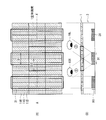
- FIG. 2 is a plan view illustrating a configuration example of the display device illustrated in FIG. 1.
- FIG. 2 is a cross-sectional view showing a first configuration example of the surface of the light guide plate in the display device shown in FIG. 1 and an explanatory view schematically showing a scattering reflection state of light rays on the surface of the light guide plate.
- FIG. 4 is a cross-sectional view illustrating a second configuration example of the surface of the light guide plate in the display device illustrated in FIG. 1 and an explanatory diagram schematically illustrating a scattering reflection state of light rays on the surface of the light guide plate.
- FIG. 6 is a cross-sectional view illustrating a third configuration example of the surface of the light guide plate in the display device illustrated in FIG. 1 and an explanatory diagram schematically illustrating a state of scattering and reflecting light rays on the surface of the light guide plate. It is a top view which shows an example of the pixel structure of a display part.
- FIG. 11 is a plan view and a cross-sectional view illustrating a first example of a correspondence relationship between an assignment pattern and a scattering area arrangement pattern when two viewpoint images are assigned in the pixel structure of FIG. 10. It is a perspective view showing the structure of the television apparatus as an electronic device using a display apparatus. It is a top view which shows the 3rd modification of the display apparatus shown in FIG.
- the display device includes a display unit 1 that performs image display, and an illumination device that is disposed on the back side of the display unit 1 and emits image display light toward the display unit 1.
- the illuminating device includes a first light source 2 (light source for 2D / 3D display), a light guide plate 3, and a second light source 7 (light source for 2D display).
- the light guide plate 3 has a first internal reflection surface 3 ⁇ / b> A disposed to face the display unit 1 and a second internal reflection surface 3 ⁇ / b> B disposed to face the second light source 7.
- the display unit 1 and the light guide plate 3 are fixed by an adhesive member 4 so as to face each other (FIG. 1).
- a minute space is generated between the display unit 1 and the light guide plate 3.
- the space thickness (that is, the gap between the display unit 1 and the light guide plate 3) is relative to the thickness of the display unit 1 or the light guide plate 3 in order to explain the path of the light beam. It is drawn greatly.
- the display device includes a control circuit for controlling the display unit 1 used for display, but the configuration is similar to a general display control circuit. Description is omitted.
- the light source device includes a control circuit that performs on (lighting) / off (non-lighting) control of the first light source 2 and the second light source 7.
- This display device can arbitrarily and selectively switch between a two-dimensional (2D) display mode on a full screen and a three-dimensional (3D) display mode on a full screen. Switching between the two-dimensional display mode and the three-dimensional display mode is performed by performing switching control of image data displayed on the display unit 1 and switching control of on / off of the first light source 2 and the second light source 7. It is possible.
- FIG. 1 schematically shows a light emission state from the light source device when only the first light source 2 is turned on (lit), which corresponds to the three-dimensional display mode.
- FIG. 2 schematically shows a light emission state from the light source device when only the second light source 7 is turned on (lit), which corresponds to the two-dimensional display mode.
- FIG. 3 schematically shows the light emission state from the light source device when both the first light source 2 and the second light source 7 are turned on (lighted), but this is also two-dimensional. It corresponds to the display mode.
- the display unit 1 is configured by using a transmissive two-dimensional display panel, for example, a transmissive liquid crystal display panel.
- a transmissive liquid crystal display panel for example, a transmissive liquid crystal display panel.
- R (red) display pixels 11R, G (green) display There are a plurality of pixels including the pixel 11G and the B (blue) display pixel 11B, and the plurality of pixels are arranged in a matrix.
- the display unit 1 performs two-dimensional image display by modulating light from the light source device for each pixel according to image data. A plurality of viewpoint images based on 3D image data and images based on 2D image data are selectively switched and displayed on the display unit 1.
- the three-dimensional image data is data including a plurality of viewpoint images corresponding to a plurality of viewing angle directions in a three-dimensional display, for example.
- the viewpoint image data is for right-eye display and left-eye display.
- a composite image including a plurality of stripe-like viewpoint images in one screen is generated and displayed.
- the first light source 2 is configured using, for example, a fluorescent lamp such as CCFL (Cold Cathode Fluorescent Lamp) or an LED (Light Emitting Diode).
- the first light source 2 emits the first illumination light L1 (FIG. 1) from the side surface direction toward the inside of the light guide plate 3.
- At least one first light source 2 is disposed on the side surface of the light guide plate 3.
- the planar shape of the light guide plate 3 is a quadrangle, there are four side surfaces, but the first light source 2 may be disposed on at least one of the side surfaces.
- FIG. 1 which has arrange
- the first light source 2 is controlled to be turned on (lighted) and turned off (not lighted) in accordance with switching between the two-dimensional display mode and the three-dimensional display mode. Specifically, the first light source 2 is controlled to be in a lighting state when displaying an image based on the three-dimensional image data on the display unit 1 (in the case of the three-dimensional display mode), and two-dimensionally displayed on the display unit 1. When an image based on image data is displayed (in the case of the two-dimensional display mode), it is controlled to a non-lighting state (light-off state) or a light-on state.
- the second light source 7 is disposed opposite to the light guide plate 3 on the side where the second internal reflection surface 3B is formed.
- the second light source 7 emits the second illumination light L10 from the outside toward the second internal reflection surface 3B (see FIGS. 2 and 3).
- the second light source 7 may be a planar light source that emits light with uniform in-plane luminance, and the structure itself is not limited to a specific one, and a commercially available planar backlight can be used. It is.
- a structure using a light emitter such as CCFL or LED and a light diffusing plate for making the in-plane luminance uniform can be considered.
- the second light source 7 is controlled to be on (lit) and off (not lit) in accordance with switching between the two-dimensional display mode and the three-dimensional display mode. Specifically, the second light source 7 is controlled to be in a non-lighting state (light-off state) when displaying an image based on the three-dimensional image data on the display unit 1 (in the case of the three-dimensional display mode). When an image based on the two-dimensional image data is displayed on the unit 1 (in the case of the two-dimensional display mode), the lighting state is controlled.
- the light guide plate 3 is made of a transparent plastic plate made of, for example, acrylic resin.
- the surface of the light guide plate 3 other than the second internal reflection surface 3B is transparent over the entire surface.
- the planar shape of the light guide plate 3 is a quadrangle
- the first internal reflection surface 3A and the four side surfaces are transparent over the entire surface.
- the first internal reflection surface 3A is mirror-finished over the entire surface, and internally reflects light rays incident at an incident angle satisfying the total reflection condition inside the light guide plate 3 and also does not satisfy the total reflection conditions. Is to be injected outside.
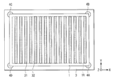
- the second internal reflection surface 3 ⁇ / b> B has a scattering area 31 and a total reflection area 32.
- the scattering area 31 is formed by laser processing, sandblasting, painting, or attaching a sheet-like light scattering member to the surface of the light guide plate 3.
- the first illumination light L1 from the first light source 2 serves as an opening (slit part) as a parallax barrier.
- the total reflection area 32 functions as a shielding part.
- the scattering area 31 and the total reflection area 32 are provided in a pattern having a structure corresponding to a parallax barrier.
- the total reflection area 32 is provided in a pattern corresponding to a shielding part in the parallax barrier
- the scattering area 31 is provided in a pattern corresponding to an opening in the parallax barrier.
- the barrier pattern of the parallax barrier for example, various types such as a striped pattern in which a large number of vertically long slit-like openings are arranged in parallel in the horizontal direction through the shielding portion are used. However, it is not limited to a specific one.
- the total reflection area 32 on the first internal reflection surface 3A and the second internal reflection surface 3B causes total internal reflection of a light beam incident at an incident angle ⁇ 1 that satisfies the total reflection condition (an incident angle larger than a predetermined critical angle ⁇ ).
- the light beam incident at ⁇ 1 is totally reflected internally).
- the first illumination light L1 from the first light source 2 incident at an incident angle ⁇ 1 that satisfies the total reflection condition satisfies the total reflection area 32 on the first internal reflection surface 3A and the second internal reflection surface 3B.
- the light is guided in the lateral direction by total internal reflection.
- the total reflection area 32 also transmits the second illumination light L10 from the second light source 7 as shown in FIG. 2 or FIG. 3, and deviates from the total reflection condition toward the first internal reflection surface 3A. It comes out as a light beam.
- the scattering area 31 scatters and reflects the first illumination light L1 from the first light source 2, and at least part of the first illumination light L1 is a first internal reflection surface. It is emitted toward 3A as a light beam (scattered light beam L20) that deviates from the total reflection condition.
- the adhesive member 4 is an adhesive made of, for example, an ultraviolet curing type or a heat effect type epoxy resin.
- the adhesive member 4 is provided, for example, so as to connect the peripheral portion of the display unit 1 and the peripheral portion of the light guide plate 3. That is, the light guide plate 3 and the display unit 1 are fixed to the whole or a part of the peripheral region surrounding the effective display region 1R by the adhesive member 4.
- the adhesive member 4 is continuously provided without being interrupted so as to surround the effective display region 1R as shown in FIG. 4, entry of moisture, foreign matter, etc. from the outside is avoided.
- the adhesive member 4 has a property of absorbing or reflecting visible light.
- the first illumination light L1 from the first light source 2 passes through the first internal reflection surface 3A of the light guide plate 3 and travels to the adhesive member 4, and then reaches the observer directly, or the display unit This is to prevent unnecessary light (stray light) that passes through 1 and reaches the observer.
- stray light may cause image quality deterioration such as a decrease in the contrast of the display image, and is desirably removed.
- a light-shielding adhesive member 4 is made of, for example, an adhesive containing carbon black.
- the transparent adhesive member 4 Even when the transparent adhesive member 4 is used, a black matrix or the like is provided between the adhesive member 4 and the facing surface 3S of the light guide plate 3 as in the first modification shown in FIG.
- the light-shielding thin film 5 may be provided in advance. Even in such a case, stray light can be avoided.
- the adhesive member 4 or the thin film 5 is made of a material having a high reflectance such as Ag (silver) or Al (aluminum), the first illumination light L1 from the light guide plate 3 is again emitted from the light guide plate 3. It can be returned to the inside of the lamp, and the light use efficiency is improved.
- the adhesive member 4 even when the transparent adhesive member 4 is used, the adhesive member 4 only needs to have a refractive index lower than that of the light guide plate 3 with respect to visible light. In this case, if the incident angle of the first illumination light L1 with respect to the first internal reflection surface 3A satisfies the total reflection condition between the light guide plate 3 and the adhesive member 4, the first internal reflection surface 3A. It is because the stray light which permeate
- the display unit 1 and the light guide plate 3 can be bonded to the entire surface including the effective display region 1R more firmly. Even in that case, since the light beam (scattered light beam L20) that deviates from the total reflection condition with respect to the first internal reflection surface 3A can pass through the effective display region 1R and travel toward the display unit 1, the display function is Secured.
- the adhesive member 4 is in contact with the opposing surfaces 1S and 3S of the display unit 1 and the light guide plate 3, and is in contact with at least one end surface of the light guide plate 3 and the display unit 1 (in FIG. 1, the end surface 1TS of the display unit 1). Is provided. With such a structure, the display unit 1 and the light guide plate 3 are more firmly fixed while securing a wider effective display region 1R in the display unit 1.
- the pixel unit of the display unit 1 and the scattering area 31 of the light guide plate 3 have a predetermined distance d. It is desirable to keep facing each other.
- an air space is formed between the display unit 1 and the light guide plate 3.
- a spacer 8 may be disposed between the optical plate 3 and the optical plate 3.
- the spacer 8 may be any material that is colorless and transparent and has little scattering, and for example, PMMA can be used.
- the spacer 8 may be provided so as to cover the entire surface of the back side of the display unit 1 and the surface of the light guide plate 3, or may be provided at least partially in order to maintain the distance d. I do not care.
- FIG. 7A shows a first configuration example of the second internal reflection surface 3 ⁇ / b> B in the light guide plate 3.
- FIG. 7B schematically shows a reflection state and a scattering state of the light beam on the second internal reflection surface 3B in the first configuration example shown in FIG.
- the first configuration example is a configuration example in which the scattering area 31 is a concave scattering area 31 ⁇ / b> A with respect to the total reflection area 32.
- Such a concave scattering area 31A can be formed by, for example, sandblasting or laser processing.
- the portion corresponding to the scattering area 31A can be formed by laser processing.
- the first illumination light L11 from the first light source 2 that is incident at the incident angle ⁇ 1 that satisfies the total reflection condition on the second internal reflection surface 3B is internally reflected in the total reflection area 32. Totally reflected.
- the concave scattering area 31A even if the incident light is incident at the same incident angle ⁇ 1 as that of the total reflection area 32, a part of the incident light of the first illumination light L12 satisfies the total reflection condition in the concave side surface portion 33. It is not satisfied, part of it is scattered and transmitted, and the other part is scattered and reflected. As shown in FIG. 1, a part or all of the scattered and reflected light beam (scattered light beam L20) is emitted toward the first internal reflection surface 3A as a light beam that does not satisfy the total reflection condition.
- FIG. 8A shows a second configuration example of the second internal reflection surface 3 ⁇ / b> B in the light guide plate 3.
- FIG. 8B schematically shows a reflection state and a scattering state of the light beam on the second internal reflection surface 3B in the second configuration example shown in FIG.
- This second configuration example is a configuration example in which the scattering area 31 is a convex scattering area 31 ⁇ / b> B with respect to the total reflection area 32.
- a convex scattering area 31B can be formed, for example, by molding the surface of the light guide plate 3 with a mold. In this case, mirror finishing is performed on the portion corresponding to the total reflection area 32 by the surface of the mold.
- the first illumination light L11 from the first light source 2 that is incident at the incident angle ⁇ 1 that satisfies the total reflection condition on the second internal reflection surface 3B is internally reflected in the total reflection area 32. Totally reflected.
- the convex scattering area 31B even if the incident light is incident at the same incident angle ⁇ 1 as that of the total reflection area 32, a part of the incident light of the first illumination light L12 satisfies the total reflection condition in the convex side surface portion 34. It is not satisfied, part of it is scattered and transmitted, and the other part is scattered and reflected. As shown in FIG. 1, a part or all of the scattered and reflected light beam (scattered light beam L20) is emitted toward the first internal reflection surface 3A as a light beam that does not satisfy the total reflection condition.
- FIG. 9A shows a third configuration example of the second internal reflection surface 3 ⁇ / b> B in the light guide plate 3.
- FIG. 9B schematically shows a reflection state and a scattering state of the light beam on the second internal reflection surface 3B in the third configuration example shown in FIG.
- the scattering area 31 is formed by processing the surface of the light guide plate 3 into a shape different from the total reflection area 32.
- the scattering area 31C according to the configuration example of FIG. 9A is not surface processed, but is formed on the surface of the light guide plate 3 corresponding to the second internal reflection surface 3B by a material different from the material of the light guide plate 3.
- the light scattering member 35 is disposed.
- the scattering area 31 ⁇ / b> C can be formed by patterning, for example, white paint (for example, barium sulfate) on the surface of the light guide plate 3 by screen printing as the light scattering member 35.
- white paint for example, barium sulfate
- the first illumination light L11 from the first light source 2 that is incident at the incident angle ⁇ 1 that satisfies the total reflection condition on the second internal reflection surface 3B is internally reflected in the total reflection area 32. Totally reflected.
- the scattering area 31C in which the light scattering member 35 is disposed even if the incident light is incident at the same incident angle ⁇ 1 as that of the total reflection area 32, a part of the incident first illumination light L12 is scattered and transmitted by the light scattering member 35. Others are scattered and reflected. Part or all of the scattered and reflected light beams are emitted toward the first internal reflection surface 3A as light beams that do not satisfy the total reflection condition.
- the display unit 1 when displaying in the three-dimensional display mode, the display unit 1 displays an image based on the three-dimensional image data, and uses the first light source 2 and the second light source 7 for three-dimensional display. On (lit) and off (non-lit) are controlled. Specifically, as shown in FIG. 1, the first light source 2 is turned on (lighted) and the second light source 7 is controlled to be turned off (non-lighted). In this state, the first illumination light L1 from the first light source 2 is repeatedly transmitted between the first internal reflection surface 3A and the total internal reflection area 32 of the second internal reflection surface 3B in the light guide plate 3.
- the light guide plate itself can have a function as a parallax barrier. That is, for the first illumination light L1 from the first light source 2, it is equivalent to a parallax barrier having the scattering area 31 as an opening (slit part) and the total reflection area 32 as a shielding part. Can function. Thereby, equivalently, three-dimensional display by the parallax barrier method in which the parallax barrier is arranged on the back side of the display unit 1 is performed.
- the display unit 1 displays an image based on the two-dimensional image data, and the first light source 2 and the second light source 7 are used for two-dimensional display. Controls on (lit) and off (not lit). Specifically, for example, as shown in FIG. 2, the first light source 2 is turned off (non-lighted) and the second light source 7 is controlled to be turned on (lighted). In this case, the second illumination light L10 from the second light source 7 is transmitted through the total reflection area 32 on the second internal reflection surface 3B, so that the total reflection condition is obtained from almost the entire surface of the first internal reflection surface 3A. Is emitted to the outside of the light guide plate 3. That is, the light guide plate 3 functions as a planar light source similar to a normal backlight. Thereby, equivalently, two-dimensional display is performed by a backlight system in which a normal backlight is arranged on the back side of the display unit 1.
- the second illumination light L10 is emitted from almost the entire surface of the light guide plate 3.
- the first light source 2 is turned on as shown in FIG. You may make it light. Thereby, for example, when only the second light source 7 is lit, if there is a difference in luminance distribution in the portion corresponding to the scattering area 31 and the total reflection area 32, the lighting state of the first light source 2 is changed. By appropriately adjusting (on / off control or adjusting the lighting amount), it is possible to optimize the luminance distribution over the entire surface. However, when performing two-dimensional display, for example, when the luminance can be sufficiently corrected on the display unit 1 side, only the second light source 7 may be turned on.
- the display unit 1 when performing display in the three-dimensional display mode, displays a plurality of viewpoint images allocated to each pixel in a predetermined allocation pattern.
- the plurality of scattering areas 31 in the light guide plate 3 are provided in a predetermined arrangement pattern corresponding to the predetermined allocation pattern.
- the pixel structure of the display unit 1 includes a plurality of pixels including a red pixel 11R, a green pixel 11G, and a blue pixel 11B, and the plurality of pixels are in a first direction (vertical). Direction) and the second direction (horizontal direction).
- the three color pixels 11R, 11G, and 11B are periodically and alternately arranged in the horizontal direction, and the same color pixels 11R, 11G, and 11B are arranged in the vertical direction.
- the combination of the pixels 11R, 11G, and 11B of three colors that are continuous in the horizontal direction is a two-dimensional combination.
- One pixel for performing color display one unit pixel for 2D color display.
- one unit pixel for 2D color display is shown by 6 pixels in the horizontal direction and 3 pixels in the vertical direction.
- FIG. 11A shows an allocation pattern and an arrangement pattern of the scattering area 31 when two viewpoint images (first and second viewpoint images) are allocated to each pixel of the display unit 1 in the pixel structure of FIG.
- FIG. 11B corresponds to a cross section taken along line A-A ′ of FIG.
- FIG. 11B schematically shows a separation state of two viewpoint images.
- one unit pixel for 2D color display is assigned as one pixel for displaying one viewpoint image.
- pixels are assigned so that the first viewpoint image and the second viewpoint image are alternately displayed in the horizontal direction.
- a combination of two unit pixels of 2D color display in the horizontal direction is a unit image (one stereoscopic pixel) as a three-dimensional display.
- FIG. 11A shows an allocation pattern and an arrangement pattern of the scattering area 31 when two viewpoint images (first and second viewpoint images) are allocated to each pixel of the display unit 1 in the pixel structure of FIG.
- FIG. 11B corresponds to a cross section taken along line A-A ′ of FIG.
- the first viewpoint image reaches only the observer's right eye 10R
- the second viewpoint image reaches only the observer's right eye 10R.
- Stereoscopic view is performed.
- the horizontal arrangement position of the scattering area 31 is arranged so as to be located at a substantially central portion of the one-unit image as a three-dimensional display.
- the horizontal width D1 of the scattering area 31 has a predetermined relationship with the width D2 of one pixel for displaying one viewpoint image.
- the width D1 of the scattering area 31 is preferably not less than 0.5 times and not more than 1.5 times the width D2.
- the width D1 of the scattering area 31 increases, the amount of light scattered in the scattering area 31 increases, and the amount of light emitted from the light guide plate 3 increases. For this reason, luminance can be increased.
- the width D1 of the scattering area 31 exceeds 1.5 times the width D2, so-called crosstalk occurs in which light from a plurality of viewpoint images is observed, which is not preferable.
- the width D1 of the scattering area 31 decreases, the amount of light scattered in the scattering area 31 decreases, and the amount of light emitted from the light guide plate 3 decreases. For this reason, the luminance is reduced. If the width D1 of the scattering area 31 is less than 0.5 times the width D2, the luminance becomes too low and the image display becomes too dark, which is not preferable.
- the light guide plate 3 constituting the backlight is provided with a function as a parallax barrier. That is, the first illumination light L1 is scattered by the scattering area 31 of the light guide plate 3, and a part or all of the light is emitted from the first internal reflection surface 3A toward the display unit 1.
- the light guide plate 3 itself functions equivalently as a parallax barrier having the scattering area 31 as an opening (slit portion). Therefore, the number of parts can be reduced and the thickness can be reduced as compared with the case of providing a parallax barrier as a separate body.
- the parallax barrier formed in the light guide plate 3 and the corresponding pixels 11R and 11G of the display unit 1 are used. , 11B is maintained with high accuracy. Therefore, the relative positional accuracy between the light guide plate 3 and the display unit 1 is improved, and a more accurate parallax image can be realized.
- the adhesive member 4 has a property of absorbing or reflecting visible light, unnecessary light passing through the adhesive member 4 can be prevented, and deterioration of image quality can be avoided. Even when the transparent adhesive member 4 is used, if the light-shielding or light-reflecting thin film 5 is separately provided, the generation of the unnecessary light can be prevented. Furthermore, if the adhesive member 4 or the thin film 5 is made of a highly reflective material, the utilization efficiency of the first illumination light L1 from the first light source 2 can be improved.
- the display device of the present technology can be applied to electronic devices for various uses, and the type of the electronic device is not particularly limited.
- This display device can be mounted on, for example, the following electronic devices.
- the configuration of the electronic device described below is merely an example, and the configuration can be changed as appropriate.
- FIG. 12 shows an external configuration of the television device.
- This television apparatus includes, for example, a video display screen unit 200 as a display device.
- the video display screen unit 200 includes a front panel 210 and a filter glass 220.
- the display device of the present technology is used as a video display portion in, for example, a tablet personal computer (PC), a notebook PC, a mobile phone, a digital still camera, a video camera, or a car navigation system in addition to the television device shown in FIG. be able to.
- PC personal computer
- notebook PC notebook PC
- mobile phone digital still camera
- video camera video camera
- car navigation system car navigation system in addition to the television device shown in FIG. be able to.
- the present technology has been described with the embodiments and the modifications.
- the present technology is not limited to these embodiments and the like, and various modifications can be made.
- the light guide plate 3 and the display unit 1 are bonded by the adhesive as the bonding member 4 has been described, but the present invention is not limited thereto.
- the light guide plate and the display unit may be fixed to each other by applying an adhesive on both sides of a reflective tape made of Al or the like.
- the adhesive member 4 is continuously provided so as to surround the effective display area 1R of the display unit 1.
- the present invention is not limited to this.
- the display unit 1 and the light guide plate 3 are locally fixed by the four adhesive members 4A to 4D discretely provided on the periphery of the display unit 1. You may make it do.
- positioning location of an adhesive member is not limited to the example shown in FIG. 13, It can change suitably.
- a lighting device having a light guide plate; A display unit fixed to face the light guide plate and performing video display using light from the light guide plate;
- the light guide plate has first and second internal reflection surfaces facing each other, At least one of the first and second internal reflection surfaces has a scattering area that scatters the first illumination light from the outside and emits the scattered light from the first internal reflection surface toward the display unit.
- Multiple display devices Multiple display devices.
- the illumination device has a first light source that irradiates the first illumination light toward the inside of the light guide plate, and second illumination light from the outside toward the second internal reflection surface of the light guide plate.
- a second light source for irradiation The display unit selectively displays an image based on 3D image data and an image based on 2D image data.
- the first light source is controlled to be in a lighting state when displaying an image based on three-dimensional image data on the display unit, and is not used when displaying an image based on two-dimensional image data on the display unit.
- the second light source is controlled to be in a non-lighting state when displaying an image based on three-dimensional image data on the display unit, and when displaying an image based on two-dimensional image data on the display unit.
- the display device according to (1) which is controlled to be in a lighting state.
- Display device (8) An electronic device provided with a display device, The display device A lighting device having a light guide plate; A display unit fixed to the light guide plate and performing video display using light from the light guide plate; The light guide plate has first and second internal reflection surfaces facing each other, At least one of the first and second internal reflection surfaces has a scattering area that scatters the first illumination light from the outside and emits the scattered light from the first internal reflection surface toward the display unit.
- Multiple electronic devices are possible.
Landscapes
- Physics & Mathematics (AREA)
- Engineering & Computer Science (AREA)
- Multimedia (AREA)
- Signal Processing (AREA)
- General Physics & Mathematics (AREA)
- Optics & Photonics (AREA)
- Nonlinear Science (AREA)
- Chemical & Material Sciences (AREA)
- Crystallography & Structural Chemistry (AREA)
- Mathematical Physics (AREA)
- Theoretical Computer Science (AREA)
- Planar Illumination Modules (AREA)
- Devices For Indicating Variable Information By Combining Individual Elements (AREA)
- Testing, Inspecting, Measuring Of Stereoscopic Televisions And Televisions (AREA)
Priority Applications (3)
| Application Number | Priority Date | Filing Date | Title |
|---|---|---|---|
| KR20147011017A KR20140089523A (ko) | 2011-11-10 | 2012-10-12 | 표시 장치 및 전자 기기 |
| US14/355,003 US20140300710A1 (en) | 2011-11-10 | 2012-10-12 | Display unit and electronic apparatus |
| CN201280053530.1A CN104024923A (zh) | 2011-11-10 | 2012-10-12 | 显示装置和电子设备 |
Applications Claiming Priority (2)
| Application Number | Priority Date | Filing Date | Title |
|---|---|---|---|
| JP2011246775A JP2013104916A (ja) | 2011-11-10 | 2011-11-10 | 表示装置および電子機器 |
| JP2011-246775 | 2011-11-10 |
Publications (1)
| Publication Number | Publication Date |
|---|---|
| WO2013069406A1 true WO2013069406A1 (ja) | 2013-05-16 |
Family
ID=48289790
Family Applications (1)
| Application Number | Title | Priority Date | Filing Date |
|---|---|---|---|
| PCT/JP2012/076522 WO2013069406A1 (ja) | 2011-11-10 | 2012-10-12 | 表示装置および電子機器 |
Country Status (6)
Cited By (1)
| Publication number | Priority date | Publication date | Assignee | Title |
|---|---|---|---|---|
| CN109410760A (zh) * | 2018-09-30 | 2019-03-01 | 云谷(固安)科技有限公司 | 柔性显示面板及其制作方法、柔性显示装置 |
Families Citing this family (10)
| Publication number | Priority date | Publication date | Assignee | Title |
|---|---|---|---|---|
| CN104282225B (zh) | 2013-07-01 | 2017-07-14 | 元太科技工业股份有限公司 | 显示装置 |
| US20150185957A1 (en) * | 2013-12-30 | 2015-07-02 | Hannstar Display Corporation | Touch naked eyes stereoscopic display |
| KR20160059783A (ko) | 2014-11-19 | 2016-05-27 | 삼성전자주식회사 | 백라이트 유닛, 이를 포함하는 디스플레이 장치 및 백라이트 유닛 제조방법 |
| US9804317B2 (en) * | 2015-02-06 | 2017-10-31 | Japan Display Inc. | Display apparatus |
| KR102330204B1 (ko) | 2016-01-07 | 2021-11-23 | 삼성전자주식회사 | 방향성 광선들의 생성 방법 및 이를 수행하는 장치들 |
| KR102399552B1 (ko) * | 2016-11-28 | 2022-05-18 | 삼성전자주식회사 | 백라이트 유닛 및 이를 포함하는 디스플레이 장치 |
| CN111936785A (zh) * | 2018-03-22 | 2020-11-13 | 日东电工株式会社 | 光学装置 |
| US11420390B2 (en) * | 2018-11-19 | 2022-08-23 | Continuous Composites Inc. | System for additively manufacturing composite structure |
| EP3976346A1 (en) * | 2019-05-28 | 2022-04-06 | Continuous Composites Inc. | System for additively manufacturing composite structure |
| US12078837B2 (en) * | 2020-08-06 | 2024-09-03 | Nitto Denko Corporation | Light deflection tape, related method and uses |
Citations (5)
| Publication number | Priority date | Publication date | Assignee | Title |
|---|---|---|---|---|
| JP2001242440A (ja) * | 2000-03-01 | 2001-09-07 | Nec Corp | フロントライトユニット及び液晶表示装置 |
| JP2002221722A (ja) * | 2001-01-29 | 2002-08-09 | Minolta Co Ltd | 反射型液晶表示装置 |
| JP2003315792A (ja) * | 2002-04-24 | 2003-11-06 | Nec Lcd Technologies Ltd | 液晶表示装置 |
| JP2007507071A (ja) * | 2003-09-27 | 2007-03-22 | コーニンクレッカ フィリップス エレクトロニクス エヌ ヴィ | 3dディスプレイ装置用バックライト |
| JP2010529515A (ja) * | 2007-06-15 | 2010-08-26 | エルジー ディスプレイ カンパニー リミテッド | ディスプレイ装置及びその製造方法 |
Family Cites Families (13)
| Publication number | Priority date | Publication date | Assignee | Title |
|---|---|---|---|---|
| JP3271695B2 (ja) * | 1996-09-20 | 2002-04-02 | シャープ株式会社 | バックライト光源および液晶表示装置 |
| TWI264573B (en) * | 2002-11-29 | 2006-10-21 | Hon Hai Prec Ind Co Ltd | Ruler for measuring dots of light guide plate and method of measuring the dots using the ruler |
| WO2004057878A2 (de) * | 2002-12-20 | 2004-07-08 | X3D Technologies Gmbh | Anordnung zur zwei- oder dreidimensionalen darstellung |
| WO2006013491A1 (en) * | 2004-07-26 | 2006-02-09 | Koninklijke Philips Electronics N.V. | Multi emission mode backlight |
| GB2426351A (en) * | 2005-05-19 | 2006-11-22 | Sharp Kk | A dual view display |
| KR101493706B1 (ko) * | 2008-12-24 | 2015-02-16 | 엘지디스플레이 주식회사 | 액정표시장치용 백라이트 유닛 |
| KR101587551B1 (ko) * | 2009-12-17 | 2016-01-21 | 삼성전자주식회사 | 3d 영상 디스플레이용 도광판 및 이를 채용한 3d 영상 디스플레이 장치 |
| JP5045826B2 (ja) * | 2010-03-31 | 2012-10-10 | ソニー株式会社 | 光源デバイスおよび立体表示装置 |
| JP4930631B2 (ja) * | 2010-09-27 | 2012-05-16 | ソニー株式会社 | 立体表示装置 |
| TW201224515A (en) * | 2010-12-13 | 2012-06-16 | Ind Tech Res Inst | Display with dimension switchable function |
| KR20120066766A (ko) * | 2010-12-15 | 2012-06-25 | 삼성전자주식회사 | 액정표시장치 및 그 구동방법 |
| KR101866244B1 (ko) * | 2011-01-17 | 2018-06-12 | 삼성전자주식회사 | 스캐닝 백라이트 유닛 및 이를 구비하는 액정 표시 장치 |
| JP4973794B1 (ja) * | 2011-04-06 | 2012-07-11 | ソニー株式会社 | 表示装置 |
-
2011
- 2011-11-10 JP JP2011246775A patent/JP2013104916A/ja not_active Abandoned
-
2012
- 2012-09-28 TW TW101136081A patent/TW201319623A/zh unknown
- 2012-10-12 WO PCT/JP2012/076522 patent/WO2013069406A1/ja active Application Filing
- 2012-10-12 CN CN201280053530.1A patent/CN104024923A/zh active Pending
- 2012-10-12 KR KR20147011017A patent/KR20140089523A/ko not_active Withdrawn
- 2012-10-12 US US14/355,003 patent/US20140300710A1/en not_active Abandoned
Patent Citations (5)
| Publication number | Priority date | Publication date | Assignee | Title |
|---|---|---|---|---|
| JP2001242440A (ja) * | 2000-03-01 | 2001-09-07 | Nec Corp | フロントライトユニット及び液晶表示装置 |
| JP2002221722A (ja) * | 2001-01-29 | 2002-08-09 | Minolta Co Ltd | 反射型液晶表示装置 |
| JP2003315792A (ja) * | 2002-04-24 | 2003-11-06 | Nec Lcd Technologies Ltd | 液晶表示装置 |
| JP2007507071A (ja) * | 2003-09-27 | 2007-03-22 | コーニンクレッカ フィリップス エレクトロニクス エヌ ヴィ | 3dディスプレイ装置用バックライト |
| JP2010529515A (ja) * | 2007-06-15 | 2010-08-26 | エルジー ディスプレイ カンパニー リミテッド | ディスプレイ装置及びその製造方法 |
Cited By (2)
| Publication number | Priority date | Publication date | Assignee | Title |
|---|---|---|---|---|
| CN109410760A (zh) * | 2018-09-30 | 2019-03-01 | 云谷(固安)科技有限公司 | 柔性显示面板及其制作方法、柔性显示装置 |
| CN109410760B (zh) * | 2018-09-30 | 2021-09-28 | 广州国显科技有限公司 | 柔性显示面板及其制作方法、柔性显示装置 |
Also Published As
| Publication number | Publication date |
|---|---|
| JP2013104916A (ja) | 2013-05-30 |
| US20140300710A1 (en) | 2014-10-09 |
| TW201319623A (zh) | 2013-05-16 |
| CN104024923A (zh) | 2014-09-03 |
| KR20140089523A (ko) | 2014-07-15 |
Similar Documents
| Publication | Publication Date | Title |
|---|---|---|
| WO2013069406A1 (ja) | 表示装置および電子機器 | |
| TWI453506B (zh) | 光源裝置及立體顯示器 | |
| JP4973794B1 (ja) | 表示装置 | |
| JP5045826B2 (ja) | 光源デバイスおよび立体表示装置 | |
| JP5674023B2 (ja) | 光源デバイスおよび表示装置 | |
| JP5545068B2 (ja) | 光源デバイスおよび立体表示装置 | |
| US20120306861A1 (en) | Light source device and display | |
| JP2012237961A (ja) | 表示装置および電子機器 | |
| WO2013069405A1 (ja) | 照明装置および表示装置、ならびに電子機器 | |
| JP2013083904A (ja) | 光源デバイスおよび表示装置、ならびに電子機器 | |
| US20140036529A1 (en) | Light source device, display unit, and electronic apparatus | |
| JP2012226294A (ja) | 光源デバイスおよび表示装置、ならびに電子機器 | |
| JP2013076725A (ja) | 光源デバイスおよび表示装置、ならびに電子機器 | |
| JP2013105005A (ja) | 光源デバイスおよび表示装置、ならびに電子機器 | |
| JP2013104915A (ja) | 光源デバイスおよび表示装置、ならびに電子機器 | |
| JP2013105675A (ja) | 照明装置、表示装置および電子機器 | |
| JP2013104914A (ja) | 光源デバイスおよび表示装置、ならびに電子機器 | |
| WO2014112258A1 (ja) | 表示装置および電子機器 | |
| JP4720207B2 (ja) | 液晶表示装置 |
Legal Events
| Date | Code | Title | Description |
|---|---|---|---|
| 121 | Ep: the epo has been informed by wipo that ep was designated in this application |
Ref document number: 12847140 Country of ref document: EP Kind code of ref document: A1 |
|
| ENP | Entry into the national phase |
Ref document number: 20147011017 Country of ref document: KR Kind code of ref document: A |
|
| WWE | Wipo information: entry into national phase |
Ref document number: 14355003 Country of ref document: US |
|
| NENP | Non-entry into the national phase |
Ref country code: DE |
|
| 122 | Ep: pct application non-entry in european phase |
Ref document number: 12847140 Country of ref document: EP Kind code of ref document: A1 |