WO2013065522A1 - 光起電力装置及びその製造方法 - Google Patents
光起電力装置及びその製造方法 Download PDFInfo
- Publication number
- WO2013065522A1 WO2013065522A1 PCT/JP2012/077313 JP2012077313W WO2013065522A1 WO 2013065522 A1 WO2013065522 A1 WO 2013065522A1 JP 2012077313 W JP2012077313 W JP 2012077313W WO 2013065522 A1 WO2013065522 A1 WO 2013065522A1
- Authority
- WO
- WIPO (PCT)
- Prior art keywords
- silicon layer
- microcrystalline silicon
- film thickness
- layer
- thickness direction
- Prior art date
- Legal status (The legal status is an assumption and is not a legal conclusion. Google has not performed a legal analysis and makes no representation as to the accuracy of the status listed.)
- Ceased
Links
Images
Classifications
-
- H—ELECTRICITY
- H10—SEMICONDUCTOR DEVICES; ELECTRIC SOLID-STATE DEVICES NOT OTHERWISE PROVIDED FOR
- H10F—INORGANIC SEMICONDUCTOR DEVICES SENSITIVE TO INFRARED RADIATION, LIGHT, ELECTROMAGNETIC RADIATION OF SHORTER WAVELENGTH OR CORPUSCULAR RADIATION
- H10F77/00—Constructional details of devices covered by this subclass
- H10F77/10—Semiconductor bodies
- H10F77/16—Material structures, e.g. crystalline structures, film structures or crystal plane orientations
- H10F77/162—Non-monocrystalline materials, e.g. semiconductor particles embedded in insulating materials
- H10F77/164—Polycrystalline semiconductors
- H10F77/1642—Polycrystalline semiconductors including only Group IV materials
- H10F77/1645—Polycrystalline semiconductors including only Group IV materials including microcrystalline silicon
-
- H—ELECTRICITY
- H10—SEMICONDUCTOR DEVICES; ELECTRIC SOLID-STATE DEVICES NOT OTHERWISE PROVIDED FOR
- H10F—INORGANIC SEMICONDUCTOR DEVICES SENSITIVE TO INFRARED RADIATION, LIGHT, ELECTROMAGNETIC RADIATION OF SHORTER WAVELENGTH OR CORPUSCULAR RADIATION
- H10F10/00—Individual photovoltaic cells, e.g. solar cells
- H10F10/10—Individual photovoltaic cells, e.g. solar cells having potential barriers
- H10F10/17—Photovoltaic cells having only PIN junction potential barriers
- H10F10/172—Photovoltaic cells having only PIN junction potential barriers comprising multiple PIN junctions, e.g. tandem cells
-
- H—ELECTRICITY
- H10—SEMICONDUCTOR DEVICES; ELECTRIC SOLID-STATE DEVICES NOT OTHERWISE PROVIDED FOR
- H10F—INORGANIC SEMICONDUCTOR DEVICES SENSITIVE TO INFRARED RADIATION, LIGHT, ELECTROMAGNETIC RADIATION OF SHORTER WAVELENGTH OR CORPUSCULAR RADIATION
- H10F71/00—Manufacture or treatment of devices covered by this subclass
- H10F71/121—The active layers comprising only Group IV materials
- H10F71/1224—The active layers comprising only Group IV materials comprising microcrystalline silicon
-
- H—ELECTRICITY
- H10—SEMICONDUCTOR DEVICES; ELECTRIC SOLID-STATE DEVICES NOT OTHERWISE PROVIDED FOR
- H10F—INORGANIC SEMICONDUCTOR DEVICES SENSITIVE TO INFRARED RADIATION, LIGHT, ELECTROMAGNETIC RADIATION OF SHORTER WAVELENGTH OR CORPUSCULAR RADIATION
- H10F77/00—Constructional details of devices covered by this subclass
- H10F77/30—Coatings
- H10F77/306—Coatings for devices having potential barriers
- H10F77/311—Coatings for devices having potential barriers for photovoltaic cells
-
- H—ELECTRICITY
- H10—SEMICONDUCTOR DEVICES; ELECTRIC SOLID-STATE DEVICES NOT OTHERWISE PROVIDED FOR
- H10P—GENERIC PROCESSES OR APPARATUS FOR THE MANUFACTURE OR TREATMENT OF DEVICES COVERED BY CLASS H10
- H10P14/00—Formation of materials, e.g. in the shape of layers or pillars
- H10P14/20—Formation of materials, e.g. in the shape of layers or pillars of semiconductor materials
- H10P14/24—Formation of materials, e.g. in the shape of layers or pillars of semiconductor materials using chemical vapour deposition [CVD]
-
- H—ELECTRICITY
- H10—SEMICONDUCTOR DEVICES; ELECTRIC SOLID-STATE DEVICES NOT OTHERWISE PROVIDED FOR
- H10P—GENERIC PROCESSES OR APPARATUS FOR THE MANUFACTURE OR TREATMENT OF DEVICES COVERED BY CLASS H10
- H10P14/00—Formation of materials, e.g. in the shape of layers or pillars
- H10P14/20—Formation of materials, e.g. in the shape of layers or pillars of semiconductor materials
- H10P14/34—Deposited materials, e.g. layers
- H10P14/3402—Deposited materials, e.g. layers characterised by the chemical composition
- H10P14/3404—Deposited materials, e.g. layers characterised by the chemical composition being Group IVA materials
- H10P14/3411—Silicon, silicon germanium or germanium
-
- H—ELECTRICITY
- H10—SEMICONDUCTOR DEVICES; ELECTRIC SOLID-STATE DEVICES NOT OTHERWISE PROVIDED FOR
- H10P—GENERIC PROCESSES OR APPARATUS FOR THE MANUFACTURE OR TREATMENT OF DEVICES COVERED BY CLASS H10
- H10P14/00—Formation of materials, e.g. in the shape of layers or pillars
- H10P14/20—Formation of materials, e.g. in the shape of layers or pillars of semiconductor materials
- H10P14/34—Deposited materials, e.g. layers
- H10P14/3451—Structure
- H10P14/3452—Microstructure
- H10P14/3456—Polycrystalline
-
- Y—GENERAL TAGGING OF NEW TECHNOLOGICAL DEVELOPMENTS; GENERAL TAGGING OF CROSS-SECTIONAL TECHNOLOGIES SPANNING OVER SEVERAL SECTIONS OF THE IPC; TECHNICAL SUBJECTS COVERED BY FORMER USPC CROSS-REFERENCE ART COLLECTIONS [XRACs] AND DIGESTS
- Y02—TECHNOLOGIES OR APPLICATIONS FOR MITIGATION OR ADAPTATION AGAINST CLIMATE CHANGE
- Y02E—REDUCTION OF GREENHOUSE GAS [GHG] EMISSIONS, RELATED TO ENERGY GENERATION, TRANSMISSION OR DISTRIBUTION
- Y02E10/00—Energy generation through renewable energy sources
- Y02E10/50—Photovoltaic [PV] energy
- Y02E10/545—Microcrystalline silicon PV cells
-
- Y—GENERAL TAGGING OF NEW TECHNOLOGICAL DEVELOPMENTS; GENERAL TAGGING OF CROSS-SECTIONAL TECHNOLOGIES SPANNING OVER SEVERAL SECTIONS OF THE IPC; TECHNICAL SUBJECTS COVERED BY FORMER USPC CROSS-REFERENCE ART COLLECTIONS [XRACs] AND DIGESTS
- Y02—TECHNOLOGIES OR APPLICATIONS FOR MITIGATION OR ADAPTATION AGAINST CLIMATE CHANGE
- Y02E—REDUCTION OF GREENHOUSE GAS [GHG] EMISSIONS, RELATED TO ENERGY GENERATION, TRANSMISSION OR DISTRIBUTION
- Y02E10/00—Energy generation through renewable energy sources
- Y02E10/50—Photovoltaic [PV] energy
- Y02E10/548—Amorphous silicon PV cells
-
- Y—GENERAL TAGGING OF NEW TECHNOLOGICAL DEVELOPMENTS; GENERAL TAGGING OF CROSS-SECTIONAL TECHNOLOGIES SPANNING OVER SEVERAL SECTIONS OF THE IPC; TECHNICAL SUBJECTS COVERED BY FORMER USPC CROSS-REFERENCE ART COLLECTIONS [XRACs] AND DIGESTS
- Y02—TECHNOLOGIES OR APPLICATIONS FOR MITIGATION OR ADAPTATION AGAINST CLIMATE CHANGE
- Y02P—CLIMATE CHANGE MITIGATION TECHNOLOGIES IN THE PRODUCTION OR PROCESSING OF GOODS
- Y02P70/00—Climate change mitigation technologies in the production process for final industrial or consumer products
- Y02P70/50—Manufacturing or production processes characterised by the final manufactured product
Definitions
- the present invention relates to a photovoltaic device and a manufacturing method thereof.
- a photovoltaic device in which a microcrystalline silicon layer is stacked as a power generation layer is used.
- the microcrystalline silicon layer includes a microcrystalline phase in which a crystalline phase is formed in amorphous silicon.
- the microcrystalline silicon layer has higher light stability than the amorphous silicon layer, and has a light absorption wavelength band different from that of the amorphous silicon layer. Utilizing such characteristics, for example, it is applied to a tandem photovoltaic device laminated with an amorphous silicon layer.
- One aspect of the present invention is a photovoltaic device that includes a microcrystalline silicon layer, and the microcrystalline silicon layer is obtained when the maximum value of the crystallization rate Xc along the film thickness direction is normalized to 1.
- the crystallization rate Xc tends to increase along the film thickness direction, and the nitrogen concentration is higher in the film thickness direction range where the crystallization rate Xc is 0.75 or more than other regions in the microcrystalline silicon layer.
- One aspect of the present invention is a method for manufacturing a photovoltaic device, which is a step of forming a microcrystalline silicon layer by converting a film forming gas containing silicon into a plasma, and crystallizing along a film thickness direction.
- the crystallinity of the microcrystalline silicon layer serving as the power generation layer can be improved, and the power generation efficiency of the photovoltaic device can be improved.
- the solar cell 100 in the embodiment of the present invention includes a substrate 10, a transparent electrode layer 12, a first photoelectric conversion unit 14, an intermediate layer 16, a second photoelectric conversion unit 18, and a back electrode. It is configured including the layer 20.
- a transparent electrode layer 12 is formed on the substrate 10.
- the substrate 10 is a light-transmitting material.
- the substrate 10 can be, for example, a glass substrate, a plastic substrate, or the like.
- the transparent electrode layer 12 is a transparent conductive film having translucency.
- the transparent electrode layer 12 is doped with tin oxide (SnO 2 ), zinc oxide (ZnO), indium tin oxide (ITO), etc. with tin (Sn), antimony (Sb), fluorine (F), aluminum (Al), etc.
- a film obtained by combining at least one kind or a plurality of kinds of the transparent conductive oxides (TCO) can be used.
- the transparent electrode layer 12 is formed by, for example, a sputtering method or an MOCVD method (thermal CVD). It is also preferable to provide unevenness (texture structure) on one or both surfaces of the substrate 10 and the transparent electrode layer 12.
- a first slit may be formed in the transparent electrode layer 12 and patterned in a strip shape.
- the slit can be formed by laser processing.
- the transparent electrode layer 12 can be patterned into a strip shape using a YAG laser having a wavelength of 1064 nm.
- the first photoelectric conversion unit 14 is formed on the transparent electrode layer 12.
- the first photoelectric conversion unit 14 is an amorphous silicon solar cell (a-Si unit).
- the first photoelectric conversion unit 14 is formed by laminating amorphous silicon films in the order of p-type, i-type, and n-type from the substrate 10 side.
- the first photoelectric conversion unit 14 can be formed by, for example, plasma enhanced chemical vapor deposition (CVD).
- CVD plasma enhanced chemical vapor deposition
- an RF plasma CVD method of 13.56 MHz is preferably applied.
- silicon-containing gas such as silane (SiH 4 ), disilane (Si 2 H 6 ), dichlorosilane (SiH 2 Cl 2 ), carbon-containing gas such as methane (CH 4 ), diborane (B 2 H 6 ), etc.
- An n-type amorphous silicon film can be stacked.
- the film thickness of the i layer of the first photoelectric conversion unit 14 is preferably 100 nm or more and 500 nm or less.
- i-type is an intrinsic semiconductor layer, and even if n-type and p-type dopant concentrations are included, n-type and p-type dopant concentrations are 5 ⁇ 10 19 / cm 3 or less. It means a semiconductor layer. Further, the p-type semiconductor layer is doped with a p-type dopant such as boron (B), and the p-type dopant concentration is 5 ⁇ 10 20 / cm 3 or more and 1 ⁇ 10 22 / cm 3 or less. To do.
- a p-type dopant such as boron (B)
- the n-type semiconductor layer means that an n-type dopant such as phosphorus (P) is doped, and the n-type dopant concentration is 5 ⁇ 10 20 / cm 3 or more and 1 ⁇ 10 22 / cm 3 or less.
- P phosphorus
- the first photoelectric conversion unit 14 can be formed under the film formation conditions shown in Table 1.
- the intermediate layer 16 is formed on the first photoelectric conversion unit 14.
- the intermediate layer 16 is preferably made of a transparent conductive oxide (TCO) such as silicon oxide (SiOx).
- TCO transparent conductive oxide
- SiOx silicon oxide
- Mg magnesium
- P phosphorus
- the transparent conductive oxide (TCO) can be formed by a plasma CVD method or a DC sputtering method.
- the film thickness of the intermediate layer 16 is preferably 50 nm or more and 200 nm or less. Note that the intermediate layer 16 may not be provided.
- the second photoelectric conversion unit 18 is formed on the intermediate layer 16.
- the second photoelectric conversion unit 18 is a microcrystalline silicon solar cell ( ⁇ c-Si unit).
- the second photoelectric conversion unit 18 is formed by stacking microcrystalline silicon films in the order of p-type, i-type, and n-type from the substrate 10 side.
- the second photoelectric conversion unit 18 can be formed by a plasma CVD method.
- As the plasma CVD method for example, an RF plasma CVD method of 13.56 MHz is preferably applied.
- the second photoelectric conversion unit 18 includes a silicon-containing gas such as silane (SiH 4 ), disilane (Si 2 H 6 ), dichlorosilane (SiH 2 Cl 2 ), a carbon-containing gas such as methane (CH 4 ), diborane (B 2).
- the film thickness of the i layer of the second photoelectric conversion unit 18 is preferably 1000 nm or more and 5000 nm or less.
- the second photoelectric conversion unit 18 can be formed under the film formation conditions shown in Table 2.
- a high nitrogen concentration region is provided in the microcrystalline silicon layer when the i-type layer is formed.
- the power for generating plasma is stopped during film formation, the gas for film formation is stopped, and the inside of the apparatus is evacuated, whereby residual nitrogen in the film formation apparatus is taken into the microcrystalline silicon layer. Accordingly, a high nitrogen concentration region having a higher nitrogen concentration than other regions in the microcrystalline silicon layer can be provided.
- the concentration of nitrogen in the microcrystalline silicon layer can be measured by secondary ion mass spectrometry (SIMS).
- FIG. 2 shows the result of SIMS measurement performed on a single film of a microcrystalline silicon layer formed on the substrate 10.
- the horizontal axis indicates the depth X of the microcrystalline silicon layer in the film thickness direction
- the vertical axis indicates the concentration A and secondary ion intensity of silicon ( 28 Si: broken line) and nitrogen (N: solid line) in SIMS measurement. Indicates.
- the high nitrogen concentration region is detected as a peak in which the nitrogen (N) concentration is increased with respect to other regions as in region a in FIG.
- a high nitrogen concentration region is provided in a film thickness range where the crystallization rate Xc is 0.75 or more.
- the crystallization rate Xc can be measured by Raman spectroscopy.
- Raman spectroscopic measurement a peak due to single crystal silicon is observed near 520 cm ⁇ 1 , and a peak due to amorphous silicon is observed near 480 cm ⁇ 1 .
- the silicon crystal becomes finer, and the peak position in the vicinity of 520 cm ⁇ 1 is shifted to the low wavenumber side, so that the half width of the peak is widened.
- a crystalline silicon oxide film with a thickness of 100 to 300 nm is formed on a glass substrate, each region in the plane of the crystalline silicon oxide film is irradiated with light having a wavelength of 514 nm, and a Raman scattering spectrum is obtained. To detect. Next, a straight line connecting the intensity at 600 cm ⁇ 1 is drawn from the intensity at 400 cm ⁇ 1 of the obtained data, and this is used as a baseline for removing the influence of noise. Then, a value calculated by applying Formula (2) from the maximum intensity Ic appearing near 520 cm ⁇ 1 after subtracting the baseline value from the measured spectrum and the maximum intensity Ia appearing near 480 cm ⁇ 1 is the crystallization rate.
- Xc. (Equation 2) Crystallization rate Xc Ic / Ia (2)
- the film thickness at which the crystallization ratio Xc is 0.75 or more is obtained by depositing a single film of a microcrystalline silicon layer on the substrate 10 under the same film formation conditions as the actual film formation conditions. This can be grasped in advance by performing Raman spectroscopic measurement on the silicon layer. Then, from the relationship between the film formation time and the film thickness of the microcrystalline silicon layer, the high nitrogen concentration region is introduced when the film formation time corresponding to the film thickness at which the crystallization rate Xc is 0.75 or more.
- FIG. 3 shows a microcrystalline silicon layer into which a high nitrogen concentration region is not introduced (comparative example) and a microcrystalline silicon layer into which a high nitrogen concentration region is introduced at a film thickness at which the crystallization rate Xc is 0.75 or more (Example). ) Shows the change in the crystallization ratio Xc with respect to the film thickness direction.
- the crystallization ratio Xc in the comparative example increases with an increase in the film thickness, but rapidly decreases when the peak value near the film thickness of 1.3 ⁇ m is exceeded, and then increases again.
- the crystallization rate Xc in the example increases with an increase in the film thickness, and maintains a high crystallization rate without greatly decreasing even when the peak value is reached.
- a second slit is formed and patterned into a strip shape.
- the second slit is formed so as to penetrate the second photoelectric conversion unit 18, the intermediate layer 16, and the first photoelectric conversion unit 14 and reach the transparent electrode layer 12.
- the second slit can be formed by, for example, laser processing. Although laser processing is not limited to this, it is preferable to use a wavelength of about 532 nm (second harmonic of a YAG laser).
- a back electrode layer 20 is formed on the second photoelectric conversion unit 18.
- the back electrode layer 20 is preferably a combination of a transparent conductive oxide (TCO) and a metal layer.
- TCO transparent conductive oxide
- tin oxide (SnO 2 ), zinc oxide (ZnO), indium tin oxide (ITO), or the like, or those doped with impurities is used.
- zinc oxide (ZnO) doped with aluminum (Al) as an impurity is used.
- the transparent conductive oxide is formed by, for example, a sputtering method or an MOCVD method (thermal CVD).
- the metal layer is a metal layer containing a metal such as silver (Ag), copper (Cu), or aluminum (Al).
- the metal layer can be formed by a sputtering method or the like.
- the metal layer may have a structure in which titanium (Ti) or the like is laminated in order to prevent oxidation of silver or the like.
- the back electrode layer 22 is embedded in the second slit, and the back electrode layer 20 and the transparent electrode layer 12 are electrically connected in the second slit. Is done.
- a third slit is formed in the back electrode layer 20 and patterned into a strip shape. The third slit is formed so as to penetrate the back electrode layer 20, the second photoelectric conversion unit 18, the intermediate layer 16, and the first photoelectric conversion unit 14 and reach the transparent electrode layer 12.
- the third slit is formed at a position where the second slit is sandwiched between the third slit and the first slit.
- the third slit can be formed by laser processing.
- a third slit is formed by irradiating a YAG laser at a position 50 ⁇ m lateral from the position of the second slit.
- a groove for separating the peripheral region and the power generation region may be formed around the solar cell 100 by laser processing.
- the back surface of the photovoltaic device 100 may be sealed with a sealing material.
- a resin such as ethylene / vinyl / acetate (EVA) or poly / vinyl / butyrate (PVB) is used as a filling layer and sealed with a sealing material through the filling layer.
- the sealing material is preferably a mechanically and chemically stable material such as a glass substrate or a plastic sheet. Thereby, it is possible to suppress moisture and the like from entering the power generation layer of the photovoltaic device 100.
- the crystallization rate Xc of the microcrystalline silicon layer of the second photoelectric conversion unit 18 can be improved, and the power generation efficiency of the photovoltaic device 100 can be increased.
Landscapes
- Photovoltaic Devices (AREA)
Abstract
光起電力装置であって、微結晶シリコン層を含み、微結晶シリコン層は、膜厚方向に沿った結晶化率Xcの最大値を1に規格化した場合に、膜厚方向に沿って結晶化率Xcが増加傾向を示し、結晶化率Xcが0.75以上の膜厚方向の範囲において、微結晶シリコン層内の他の領域よりも窒素濃度が高い高窒素濃度領域(領域a)を有する。
Description
本発明は、光起電力装置及びその製造方法に関する。
太陽光を利用した発電システムとして、微結晶シリコン層を発電層として積層した光起電力装置が用いられている。微結晶シリコン層は、アモルファスシリコンの中に結晶相を形成した微結晶相を含むものであり、アモルファスシリコン層に比べて光安定性が高く、アモルファスシリコン層と光の吸収波長帯が異なる。このような特性を利用して、例えば、アモルファスシリコン層と積層したタンデム型の光起電力装置等に適用されている。
しかしながら、微結晶シリコン層を発電層とした場合、その発電効率は微結晶シリコン層の結晶性に大きく影響される。そこで、微結晶シリコン層の成膜の際に、膜厚方向に水素含有率を変化させて膜質を改善する方法が開示されている(例えば、特許文献1参照)。
ところで、微結晶シリコン層を発電層とする光起電力装置ではさらなる発電効率の向上が望まれている。そこで、微結晶シリコン層の結晶性をより高める技術が必要とされている。
本発明の1つの態様は、光起電力装置であって、微結晶シリコン層を含み、微結晶シリコン層は、膜厚方向に沿った結晶化率Xcの最大値を1に規格化した場合に、膜厚方向に沿って結晶化率Xcが増加傾向を示し、結晶化率Xcが0.75以上の膜厚方向の範囲において、微結晶シリコン層内の他の領域よりも窒素濃度が高い高窒素濃度領域を有する、光起電力装置である。
本発明の1つの態様は、光起電力装置の製造方法であって、シリコンを含む成膜用ガスをプラズマ化して微結晶シリコン層を形成する工程であって、膜厚方向に沿った結晶化率Xcの最大値を1に規格化した場合に、膜厚方向に沿って増加傾向を示す結晶化率Xcが0.75以上の膜厚方向の範囲において成膜用ガスの供給を停止させる工程を備える。
本発明によれば、発電層となる微結晶シリコン層の結晶性を高め、光起電力装置の発電効率を向上させることができる。
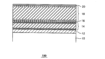
本発明の実施の形態における太陽電池100は、図1の断面図に示すように、基板10、透明電極層12、第1光電変換ユニット14、中間層16、第2光電変換ユニット18及び裏面電極層20を含んで構成される。
基板10上に透明電極層12を形成する。基板10は、透光性を有する材料とする。基板10は、例えば、ガラス基板、プラスチック基板等とすることができる。透明電極層12は、透光性を有する透明導電膜とする。透明電極層12は、酸化錫(SnO2)、酸化亜鉛(ZnO)、インジウム錫酸化物(ITO)等に錫(Sn)、アンチモン(Sb)、フッ素(F)、アルミニウム(Al)等をドープした透明導電性酸化物(TCO)のうち少なくとも一種類又は複数種を組み合わせた膜を用いることができる。透明電極層12は、例えば、スパッタリング法、MOCVD法(熱CVD)により形成する。基板10と透明電極層12の一方又は両方の表面に凹凸(テクスチャ構造)を設けることも好適である。
複数の光電変換セルを直列に接続する構造とする場合、透明電極層12に第1のスリットを形成して短冊状にパターニングしてもよい。スリットは、レーザ加工により形成することができる。例えば、波長1064nmのYAGレーザを用いて透明電極層12を短冊状にパターニングすることができる。
透明電極層12上に第1光電変換ユニット14を形成する。本実施の形態では、第1光電変換ユニット14は非晶質(アモルファス)シリコン太陽電池(a-Siユニット)とする。
第1光電変換ユニット14は、基板10側からp型、i型、n型の順にアモルファスシリコン膜を積層して形成する。第1光電変換ユニット14は、例えば、プラズマ化学気相成長法(CVD)により形成することができる。プラズマCVD法は、例えば、13.56MHzのRFプラズマCVD法を適用することが好適である。このとき、シラン(SiH4)、ジシラン(Si2H6)、ジクロルシラン(SiH2Cl2)等のシリコン含有ガス、メタン(CH4)等の炭素含有ガス、ジボラン(B2H6)等のp型ドーパント含有ガス、フォスフィン(PH3)等のn型ドーパント含有ガス及び水素(H2)等の希釈ガスを混合した混合ガスをプラズマ化して成膜を行うことによって、p型、i型、n型のアモルファスシリコン膜を積層することができる。第1光電変換ユニット14のi層の膜厚は100nm以上500nm以下とすることが好適である。
本実施の形態において、i型とは真性の半導体層であり、n型及びp型のドーパント濃度を含んでいたとしても、n型及びp型のドーパント濃度が5×10¹⁹/cm3以下の半導体層を意味する。また、p型の半導体層は、ボロン(B)等のp型のドーパントがドープされ、p型のドーパント濃度が5×1020/cm3以上1×1022/cm3以下であることを意味する。n型の半導体層は、燐(P)等のn型のドーパントがドープされ、n型のドーパント濃度が5×1020/cm3以上1×1022/cm3以下であることを意味する。
例えば、第1光電変換ユニット14は、表1の成膜条件で形成することができる。

第1光電変換ユニット14上に中間層16を形成する。本実施の形態では、中間層16は、酸化シリコン(SiOx)等の透明導電性酸化物(TCO)とすることが好適である。特に、マグネシウム(Mg)やリン(P)がドープされた酸化シリコン(SiOx)を用いることが好適である。透明導電性酸化物(TCO)は、プラズマCVD法又はDCスパッタリング法により形成することができる。中間層16の膜厚は、50nm以上200nm以下とすることが好適である。なお、中間層16を設けない構成としてもよい。
中間層16上に第2光電変換ユニット18を形成する。本実施の形態では、第2光電変換ユニット18は微結晶シリコン太陽電池(μc-Siユニット)とする。
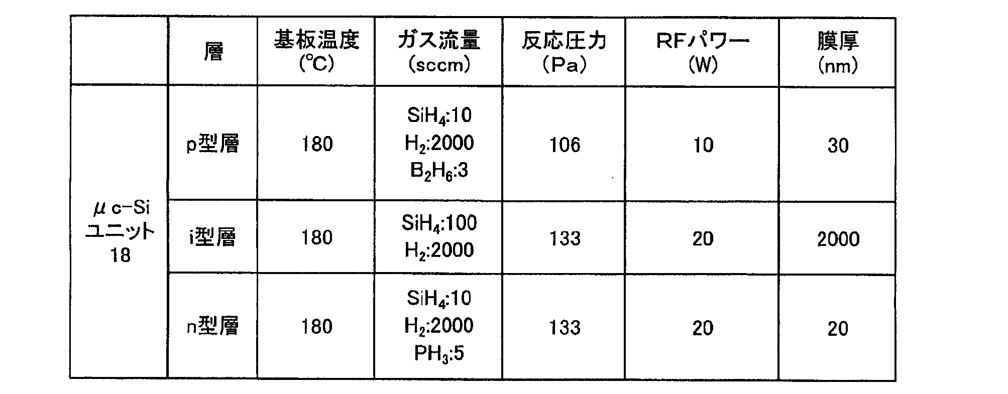
第2光電変換ユニット18は、基板10側からp型、i型、n型の順に微結晶シリコン膜を積層して形成する。第2光電変換ユニット18は、プラズマCVD法により形成することができる。プラズマCVD法は、例えば、13.56MHzのRFプラズマCVD法を適用することが好適である。第2光電変換ユニット18は、シラン(SiH4)、ジシラン(Si2H6)、ジクロルシラン(SiH2Cl2)等のシリコン含有ガス、メタン(CH4)等の炭素含有ガス、ジボラン(B2H6)等のp型ドーパント含有ガス、フォスフィン(PH3)等のn型ドーパント含有ガス及び水素(H2)等の希釈ガスを混合した混合ガスをプラズマ化して成膜を行うことによって形成することができる。第2光電変換ユニット18のi層の膜厚は1000nm以上5000nm以下とすることが好適である。
例えば、第2光電変換ユニット18は、表2の成膜条件で形成することができる。
本実施の形態では、i型層を形成する際に微結晶シリコン層内に高窒素濃度領域を設ける。成膜中にプラズマ発生用の電力を停止させると共に、成膜用のガスを停止させ、装置内を真空排気させることによって、成膜装置内の残留窒素が微結晶シリコン層に取り込まれる。これによって微結晶シリコン層内の他の領域よりも窒素濃度の高い高窒素濃度領域を設けることができる。
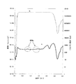
微結晶シリコン層内の窒素の濃度は、二次イオン質量分析法(SIMS)により測定することができる。図2は、基板10上に形成した微結晶シリコン層の単膜に対してSIMS測定を行った結果を示す。図2において、横軸は微結晶シリコン層の膜厚方向の深さXを示し、縦軸はSIMS測定におけるシリコン(28Si:破線)と窒素(N:実線)の濃度A及び二次イオン強度を示す。
高窒素濃度領域は、図2における領域aのように他の領域に対して窒素(N)濃度が増加したピークとして検出される。本実施の形態では、高窒素濃度領域は、微結晶シリコン層の深さX1における窒素(N)の濃度AN1に対して、深さX1から50nm離れた深さX2(=X1+50nm)の濃度AN2が3%以上変化した領域として定義される。すなわち、高窒素濃度領域は、以下の数式(1)を満足する領域である。
(数1)
(AN2-AN1)/AN1≧0.03(=3%)・・・(1)
(数1)
(AN2-AN1)/AN1≧0.03(=3%)・・・(1)
本実施の形態では、微結晶シリコン層の結晶化率のピーク値(最大値)を1に規格化した場合において、結晶化率Xcが0.75以上の膜厚範囲において高窒素濃度領域を設ける。
結晶化率Xcは、ラマン分光測定により測定することができる。ラマン分光測定では、520cm-1付近に単結晶シリコンに起因するピークがみられ、480cm-1付近にアモルファスシリコンに起因するピークがみられる。微結晶シリコン層では、シリコン結晶が微粒子化すると共に520cm-1近傍のピーク位置が低波数側にシフトしピークの半値幅が広がる。
本実施の形態では、ガラス基板上に100~300nmの結晶質の酸化シリコン膜を形成し、結晶質の酸化シリコン膜の面内の各領域に波長514nmの光を照射し、ラマン散乱のスペクトルを検出する。次に、得られたデータの400cm-1での強度から600cm-1での強度を結ぶ直線を引き、これをノイズの影響を除去するベースラインとする。そして、測定スペクトルからベースラインの値を引いた後の520cm-1付近に現われる最大強度Icと、480cm-1付近に現われる最大強度Iaから数式(2)を適用して算出した値を結晶化率Xcとした。
(数2)
結晶化率Xc=Ic/Ia・・・(2)
(数2)
結晶化率Xc=Ic/Ia・・・(2)
結晶化率Xcが0.75以上となる膜厚は、実際の成膜条件と同じ成膜条件下において基板10上に微結晶シリコン層の単膜を成膜し、様々な膜厚の微結晶シリコン層に対してラマン分光測定を行うことにより予め把握することができる。そして、成膜時間と微結晶シリコン層の膜厚との関係から、結晶化率Xcが0.75以上となる膜厚に相当する成膜時間経過時に高窒素濃度領域を導入する。
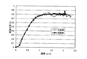
図3は、高窒素濃度領域を導入していない微結晶シリコン層(比較例)及び結晶化率Xcが0.75以上となる膜厚において高窒素濃度領域を導入した微結晶シリコン層(実施例)の膜厚方向に対する結晶化率Xcの変化を示す。比較例における結晶化率Xcは、膜厚の増加とともに増加するが、膜厚1.3μm付近のピーク値を越えると急激に低下し、その後再び増加する。一方、実施例における結晶化率Xcは、膜厚の増加と共に増加し、ピーク値を迎えても大きく低下することなく高い結晶化率を維持する。
このように、結晶化率Xcが0.75以上となる膜厚において高窒素濃度領域を導入することによって、微結晶シリコン層の結晶化率Xcが低下する膜厚方向の領域が生ずることを抑制でき、これによって第2光電変換ユニット18における発電効率を高めることができる。
複数の光電変換セルを直列に接続する構造とする場合、第2のスリットを形成して短冊状にパターニングする。第2のスリットは、第2光電変換ユニット18,中間層16,第1光電変換ユニット14を貫いて透明電極層12に到達するように形成する。第2のスリットは、例えば、レーザ加工により形成することができる。レーザ加工は、これに限定されるものではないが、波長約532nm(YAGレーザの第2高調波)を用いて行うことが好適である。
第2光電変換ユニット18上に裏面電極層20を形成する。裏面電極層20は、透明導電性酸化物(TCO)と金属層との組み合わせとすることが好適である。透明導電性酸化物は、酸化錫(SnO2)、酸化亜鉛(ZnO)、インジウム錫酸化物(ITO)等、又は、これらに不純物をドープしたものが用いられる。例えば、酸化亜鉛(ZnO)にアルミニウム(Al)を不純物としてドープしたものが用いられる。透明導電性酸化物は、例えば、スパッタリング法、MOCVD法(熱CVD)により形成する。金属層は、銀(Ag)、銅(Cu)、アルミニウム(Al)等の金属を含む金属層とする。特に、反射率及び導電率の高さから銀(Ag)を用いることが好適である。金属層は、スパッタリング法等により形成することができる。また、金属層は、銀等の酸化を防ぐためにチタン(Ti)等を積層した構造としてもよい。
複数の光電変換セルを直列に接続する構造とする場合、裏面電極層22は、第2のスリットに埋め込まれ、第2のスリット内で裏面電極層20と透明電極層12とが電気的に接続される。さらに、裏面電極層20に第3のスリットを形成して短冊状にパターニングする。第3のスリットは、裏面電極層20、第2光電変換ユニット18、中間層16、第1光電変換ユニット14を貫いて透明電極層12に到達するように形成する。第3のスリットは、第1のスリットとの間に第2のスリットを挟む位置に形成する。第3のスリットは、レーザ加工により形成することができる。例えば、第2のスリットの位置から50μm横の位置にYAGレーザを照射して第3のスリットを形成する。さらに、レーザ加工により太陽電池100の周辺に周辺領域と発電領域とを分離する溝を形成してもよい。
光起電力装置100の裏面は、封止材によって封止してもよい。エチレン・ビニル・アセテート(EVA)やポリ・ビニル・ブチラート(PVB)等の樹脂を充填層として、充填層を介して封止材により封止する。封止材は、ガラス基板やプラスチックシート等の機械的及び化学的に安定な材料とすることが好ましい。これによって、光起電力装置100の発電層への水分等の浸入を抑制することができる。
以上のように、本実施の形態では、第2光電変換ユニット18の微結晶シリコン層の結晶化率Xcを向上させることができ、光起電力装置100の発電効率を高めることができる。
10 基板、12 透明電極層、14 第1光電変換ユニット、16 中間層、18 第2光電変換ユニット、20 裏面電極層、100 太陽電池。
Claims (3)
- 光起電力装置であって、
微結晶シリコン層を含み、
前記微結晶シリコン層は、膜厚方向に沿った結晶化率Xcの最大値を1に規格化した場合に、膜厚方向に沿って前記結晶化率Xcが増加傾向を示し、前記結晶化率Xcが0.75以上の膜厚方向の範囲において、前記微結晶シリコン層内の他の領域よりも窒素濃度が高い高窒素濃度領域を有する。 - 請求項1に記載の光起電力装置であって、
前記高窒素濃度領域は、前記微結晶シリコン層の深さX1における窒素(N)の濃度AN1に対して、深さX1から50nm離れた深さX2(=X1+50nm)の濃度AN2が3%以上変化した領域である。 - 光起電力装置の製造方法であって、
シリコンを含む成膜用ガスをプラズマ化して微結晶シリコン層を形成する工程であって、膜厚方向に沿った結晶化率Xcの最大値を1に規格化した場合に、膜厚方向に沿って増加傾向を示す前記結晶化率Xcが0.75以上の膜厚方向の範囲において前記成膜用ガスの供給を停止させる工程を備える。
Priority Applications (1)
| Application Number | Priority Date | Filing Date | Title |
|---|---|---|---|
| US13/893,438 US20130240038A1 (en) | 2011-10-31 | 2013-05-14 | Photovoltaic device and manufacturing method thereof |
Applications Claiming Priority (2)
| Application Number | Priority Date | Filing Date | Title |
|---|---|---|---|
| JP2011-239077 | 2011-10-31 | ||
| JP2011239077 | 2011-10-31 |
Related Child Applications (1)
| Application Number | Title | Priority Date | Filing Date |
|---|---|---|---|
| US13/893,438 Continuation US20130240038A1 (en) | 2011-10-31 | 2013-05-14 | Photovoltaic device and manufacturing method thereof |
Publications (1)
| Publication Number | Publication Date |
|---|---|
| WO2013065522A1 true WO2013065522A1 (ja) | 2013-05-10 |
Family
ID=48191876
Family Applications (1)
| Application Number | Title | Priority Date | Filing Date |
|---|---|---|---|
| PCT/JP2012/077313 Ceased WO2013065522A1 (ja) | 2011-10-31 | 2012-10-23 | 光起電力装置及びその製造方法 |
Country Status (2)
| Country | Link |
|---|---|
| US (1) | US20130240038A1 (ja) |
| WO (1) | WO2013065522A1 (ja) |
Citations (4)
| Publication number | Priority date | Publication date | Assignee | Title |
|---|---|---|---|---|
| JPH11274527A (ja) * | 1998-03-24 | 1999-10-08 | Sanyo Electric Co Ltd | 光起電力装置 |
| JP2005294457A (ja) * | 2004-03-31 | 2005-10-20 | Tokyo Electron Ltd | 成膜方法及び成膜装置 |
| JP2011155026A (ja) * | 2009-12-11 | 2011-08-11 | Mitsubishi Heavy Ind Ltd | 光電変換装置の製造方法 |
| WO2011132775A1 (ja) * | 2010-04-22 | 2011-10-27 | 京セラ株式会社 | 薄膜太陽電池の製造方法 |
-
2012
- 2012-10-23 WO PCT/JP2012/077313 patent/WO2013065522A1/ja not_active Ceased
-
2013
- 2013-05-14 US US13/893,438 patent/US20130240038A1/en not_active Abandoned
Patent Citations (4)
| Publication number | Priority date | Publication date | Assignee | Title |
|---|---|---|---|---|
| JPH11274527A (ja) * | 1998-03-24 | 1999-10-08 | Sanyo Electric Co Ltd | 光起電力装置 |
| JP2005294457A (ja) * | 2004-03-31 | 2005-10-20 | Tokyo Electron Ltd | 成膜方法及び成膜装置 |
| JP2011155026A (ja) * | 2009-12-11 | 2011-08-11 | Mitsubishi Heavy Ind Ltd | 光電変換装置の製造方法 |
| WO2011132775A1 (ja) * | 2010-04-22 | 2011-10-27 | 京セラ株式会社 | 薄膜太陽電池の製造方法 |
Also Published As
| Publication number | Publication date |
|---|---|
| US20130240038A1 (en) | 2013-09-19 |
Similar Documents
| Publication | Publication Date | Title |
|---|---|---|
| JP4940290B2 (ja) | 光電変換装置及びその製造方法 | |
| JP4902779B2 (ja) | 光電変換装置及びその製造方法 | |
| WO2013002102A1 (ja) | 光電変換装置 | |
| JP2010283161A (ja) | 太陽電池及びその製造方法 | |
| US20100206373A1 (en) | Photovoltaic device | |
| US8088641B2 (en) | Process for producing photovoltaic device | |
| US8759667B2 (en) | Photoelectric conversion device | |
| JP4764469B2 (ja) | 光電変換装置及び光電変換装置の製造方法 | |
| JP2008283075A (ja) | 光電変換装置の製造方法 | |
| WO2013121817A1 (ja) | 集積型光電変換装置、その製造方法および太陽電池 | |
| JP4875566B2 (ja) | 光電変換装置の製造方法 | |
| JP2011014618A (ja) | 太陽電池及びその製造方法 | |
| WO2011070805A1 (ja) | 光電変換装置の製造方法 | |
| JP2010283162A (ja) | 太陽電池及びその製造方法 | |
| JP5373045B2 (ja) | 光電変換装置 | |
| WO2011105166A1 (ja) | 光電変換モジュール及びその製造方法 | |
| US20130240038A1 (en) | Photovoltaic device and manufacturing method thereof | |
| WO2012081656A1 (ja) | 光電変換装置及びその製造方法 | |
| WO2013125251A1 (ja) | 薄膜太陽電池 | |
| WO2010146846A1 (ja) | 光電変換装置及び光電変換装置の製造方法 | |
| WO2013080803A1 (ja) | 光起電力装置 | |
| JP2013098249A (ja) | 光起電力装置及びその製造方法 | |
| JP2013065751A (ja) | 太陽電池 | |
| JP2010283159A (ja) | 太陽電池及びその製造方法 | |
| JP2013115339A (ja) | 光起電力装置 |
Legal Events
| Date | Code | Title | Description |
|---|---|---|---|
| 121 | Ep: the epo has been informed by wipo that ep was designated in this application |
Ref document number: 12845418 Country of ref document: EP Kind code of ref document: A1 |
|
| NENP | Non-entry into the national phase |
Ref country code: DE |
|
| 122 | Ep: pct application non-entry in european phase |
Ref document number: 12845418 Country of ref document: EP Kind code of ref document: A1 |
|
| NENP | Non-entry into the national phase |
Ref country code: JP |