WO2013054465A1 - 絶縁ゲート型デバイスの駆動回路 - Google Patents
絶縁ゲート型デバイスの駆動回路 Download PDFInfo
- Publication number
- WO2013054465A1 WO2013054465A1 PCT/JP2012/005566 JP2012005566W WO2013054465A1 WO 2013054465 A1 WO2013054465 A1 WO 2013054465A1 JP 2012005566 W JP2012005566 W JP 2012005566W WO 2013054465 A1 WO2013054465 A1 WO 2013054465A1
- Authority
- WO
- WIPO (PCT)
- Prior art keywords
- gate
- voltage
- mosfet
- vin
- power mosfet
- Prior art date
- Legal status (The legal status is an assumption and is not a legal conclusion. Google has not performed a legal analysis and makes no representation as to the accuracy of the status listed.)
- Ceased
Links
Images







Classifications
-
- H—ELECTRICITY
- H03—ELECTRONIC CIRCUITRY
- H03K—PULSE TECHNIQUE
- H03K17/00—Electronic switching or gating, i.e. not by contact-making and –breaking
- H03K17/06—Modifications for ensuring a fully conducting state
-
- F—MECHANICAL ENGINEERING; LIGHTING; HEATING; WEAPONS; BLASTING
- F02—COMBUSTION ENGINES; HOT-GAS OR COMBUSTION-PRODUCT ENGINE PLANTS
- F02P—IGNITION, OTHER THAN COMPRESSION IGNITION, FOR INTERNAL-COMBUSTION ENGINES; TESTING OF IGNITION TIMING IN COMPRESSION-IGNITION ENGINES
- F02P3/00—Other installations
- F02P3/02—Other installations having inductive energy storage, e.g. arrangements of induction coils
- F02P3/04—Layout of circuits
- F02P3/05—Layout of circuits for control of the magnitude of the current in the ignition coil
- F02P3/051—Opening or closing the primary coil circuit with semiconductor devices
- F02P3/053—Opening or closing the primary coil circuit with semiconductor devices using digital techniques
-
- F—MECHANICAL ENGINEERING; LIGHTING; HEATING; WEAPONS; BLASTING
- F02—COMBUSTION ENGINES; HOT-GAS OR COMBUSTION-PRODUCT ENGINE PLANTS
- F02P—IGNITION, OTHER THAN COMPRESSION IGNITION, FOR INTERNAL-COMBUSTION ENGINES; TESTING OF IGNITION TIMING IN COMPRESSION-IGNITION ENGINES
- F02P3/00—Other installations
- F02P3/02—Other installations having inductive energy storage, e.g. arrangements of induction coils
- F02P3/04—Layout of circuits
- F02P3/055—Layout of circuits with protective means to prevent damage to the circuit, e.g. semiconductor devices or the ignition coil
- F02P3/0552—Opening or closing the primary coil circuit with semiconductor devices
- F02P3/0554—Opening or closing the primary coil circuit with semiconductor devices using digital techniques
-
- F—MECHANICAL ENGINEERING; LIGHTING; HEATING; WEAPONS; BLASTING
- F02—COMBUSTION ENGINES; HOT-GAS OR COMBUSTION-PRODUCT ENGINE PLANTS
- F02P—IGNITION, OTHER THAN COMPRESSION IGNITION, FOR INTERNAL-COMBUSTION ENGINES; TESTING OF IGNITION TIMING IN COMPRESSION-IGNITION ENGINES
- F02P9/00—Electric spark ignition control, not otherwise provided for
- F02P9/002—Control of spark intensity, intensifying, lengthening, suppression
- F02P9/005—Control of spark intensity, intensifying, lengthening, suppression by weakening or suppression of sparks to limit the engine speed
-
- H—ELECTRICITY
- H03—ELECTRONIC CIRCUITRY
- H03K—PULSE TECHNIQUE
- H03K17/00—Electronic switching or gating, i.e. not by contact-making and –breaking
- H03K17/06—Modifications for ensuring a fully conducting state
- H03K2017/066—Maximizing the OFF-resistance instead of minimizing the ON-resistance
Definitions
- the present invention relates to a drive circuit for an insulated gate device, and more particularly to a drive circuit for an insulated gate device that prevents rare-on of the device.
- FIG. 11 is a circuit diagram showing a configuration of a driving circuit of a conventional insulated gate device.
- a load 102 such as a resistance load or an inductive load is connected to a power source 101, and the other end of the load 102 is connected to a load drive control element (high function MOSFET) 103.
- the load drive control element 103 has three terminals: a drain terminal 104, a gate terminal 105, and a source terminal 106.
- the drain terminal 104 is connected to the other end of the load 102, and the source terminal 106 is connected to the ground.
- a gate signal is input to the gate terminal 105 from the outside.
- the load drive control element 103 includes a drive circuit unit 117 and a power unit 118, and the drive circuit unit 117 and the power unit 118 are formed in one semiconductor chip.
- the power unit 118 includes a power MOSFET 108.
- the power MOSFET 108 is an insulated gate device that is on / off controlled by the drive circuit unit 117.
- a temperature detection sensor 111 for detecting temperature and logic for performing signal processing of the temperature detection sensor 111.
- a circuit 112 and a gate voltage control MOSFET 114 that receives a signal from the logic circuit 112 and controls shutdown of the gate potential 123 are provided.
- a current detection sensor 110 is provided between the drain potential 122 and the ground potential (source potential) 124, and the current detection sensor 110 is interposed between the gate potential 123 and the ground potential (source potential) 124.
- a gate voltage control circuit 115 that receives the signal and controls the voltage level of the gate potential 123 is also provided.
- a diode 109, an input resistor 113, and a diode 125 are provided between the gate potential 123 and the ground potential (source potential) 124.
- a connection point between the diode 109 and the input resistor 113 is connected to the gate terminal 105.
- a constant current source 116 for pulling down the gate potential 123 is provided between the gate potential 123 and the ground potential (source potential) 124 so that the power MOSFET 108 is not erroneously turned on even when noise occurs in the gate terminal 105.
- a pull-down resistor 126 is provided between the gate potential 123 and the ground potential (source potential) 124.
- the load drive control element 103 functions as a switching element for driving the load 102.
- the load drive control element 103 has an overload for preventing the load drive control element 103 itself from being destroyed by a large current flowing through the load drive control element 103 when the load 102 is short-circuited. It has a current detection function, an overheat detection function for preventing the load drive control element 103 itself from being destroyed by heat generated by the large current, and a switching element gate protection function.
- the overheat detection function and the overcurrent detection function operate using the gate voltage as a power source.
- the overheat detection function operates as follows. That is, when the voltage of the output (input of the logic circuit 112) 121 of the temperature detection sensor 111 reaches a predetermined voltage as the temperature rises, the logic circuit 112 sets the voltage control MOSFET 114 to the gate 119 of the gate voltage control MOSFET 114. Apply voltage to turn on. As a result, the gate potential 123 is set lower than the threshold voltage of the power MOSFET 108 to turn off the power MOSFET 108 and turn off the load drive control element 103.
- the overcurrent detection function operates as follows. That is, when the current 120 flowing from the drain terminal 104 and the ground terminal (source terminal) 106 increases and the input 120 from the current detection sensor 110 to the gate voltage control circuit 115 reaches a predetermined voltage, the gate voltage control is performed. The circuit 115 limits the current flowing between the drain terminal 104 and the ground terminal (source terminal) 106 by reducing the gate potential 123.
- the input resistor 113, the diode 125, and the pull-down resistor 126 also have a threshold value determining function for determining the threshold value VIN (th) of the load drive control element 103.
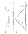
- FIG. 12 is a timing chart showing an example of the threshold value determining function. Here, the voltage Vin of the gate terminal 105, the gate voltage Vg (gate potential 123), and the drain voltage Vd (drain potential 122) of the power MOSFET 108 when a triangular wave is input to the gate terminal 105 are shown.
- FIG. 12 shows a case where the gate voltage Vg (gate potential 123) is determined by dividing the voltage Vin of the gate terminal 105 of FIG. 11 by the voltage dividing ratio of the input resistor 113 and the pull-down resistor 126. That is, here, the gate voltage Vg (gate potential 123) is adjusted to be equal to or higher than the threshold voltage Vg (th) of the power MOSFET 108 by adjusting the gate voltage Vg (gate potential 123) by the voltage dividing ratio of the input resistor 113 and the pull-down resistor 126. The timing to become is adjusted. In this way, the threshold value VIN (th) of the load drive control element 103 is adjusted.
- Patent Document 1 As a technique for effectively reducing a surge voltage and a turn-off loss generated when the power MOSFET is turned off, there is a technique described in Patent Document 1, for example.
- This technology includes a current source circuit that discharges a gate capacitance when the current flowing through the main terminal of the power MOSFET is turned off, and a current adjustment circuit that adjusts a current value for discharging the gate capacitance via the current source circuit. Is.
- a current source circuit is connected when the power MOSFET is turned off by a gate signal, and the current source circuit is disconnected when the power MOSFET is turned on.
- the output current of the current source circuit is made variable, and the current adjustment circuit keeps the output current of the current source circuit constant until the voltage across the main terminal of the power MOSFET starts to rise. As the voltage increases, the output current of the current source circuit is gradually reduced.
- the threshold value VIN (th) of the load drive control element 103 can be adjusted to an arbitrary voltage as shown in FIGS.
- the gate voltage Vg (gate potential 123) of the power MOSFET 108 drops compared to the voltage Vin of the gate terminal 105. Resistance becomes high.
- the threshold VIN (th) is adjusted using the diode 125, the voltage drop can be made constant regardless of the magnitude of the voltage Vin at the gate terminal 105. . Therefore, compared to the case where the threshold value VIN (th) is adjusted using the pull-down resistor 126 ( ⁇ in FIG. 12), the increase in the on-resistance of the power MOSFET 108 can be stopped. However, since it is impossible to prevent the voltage drop from occurring, it is impossible to prevent the on-resistance of the power MOSFET 108 from increasing.
- an object of the present invention is to provide a drive circuit for an insulated gate device that can prevent rare ON of the device.
- a first aspect of the present invention includes a gate voltage control semiconductor element connected between a gate and a source of an insulated gate semiconductor element and driven by a gate signal input from the outside,
- the threshold voltage of the gate voltage control semiconductor element is set lower than the threshold voltage of the insulated gate semiconductor element, and the voltage value of the gate signal is equal to or higher than the threshold voltage of the gate voltage control semiconductor element.
- the gate voltage control semiconductor element is controlled to be turned on.
- the threshold voltage of the gate voltage control semiconductor element when the threshold voltage of the gate voltage control semiconductor element is set lower than the threshold voltage of the insulated gate semiconductor element, and the voltage value of the gate signal is equal to or higher than the threshold voltage of the gate voltage control semiconductor element and lower than the reference voltage. Then, the gate voltage control semiconductor element is driven and controlled to be turned on. Thereby, in the process of increasing the voltage value of the gate signal, the voltage value of the gate signal can reach the threshold voltage of the insulated gate semiconductor element after reaching the threshold voltage of the gate voltage controlling semiconductor element.
- the second aspect of the present invention may include a threshold control circuit for driving and controlling the gate voltage control semiconductor element, and the reference voltage of the threshold control circuit may be arbitrarily set. Thereby, it is possible to arbitrarily adjust the voltage value at which the insulated gate semiconductor element is turned on.
- the threshold voltage of the gate voltage control semiconductor element is set lower than the threshold voltage of the insulated gate semiconductor element, and the voltage value of the gate signal is equal to or higher than the threshold voltage of the gate voltage control semiconductor element and higher than the reference voltage.
- the gate voltage control semiconductor element is driven and controlled to be turned on, so that it is possible to prevent rare ON of the insulated gate semiconductor element in the region where the voltage value of the gate signal is lower than the reference voltage, and to prevent the occurrence of leakage current. .
- the gate voltage of the insulated gate semiconductor element does not drop with respect to the voltage value of the gate signal, thereby preventing the on-resistance of the insulated gate semiconductor element from increasing. can do.
- FIG. 5 is an operation waveform diagram of the logic circuit of FIG. 4.
- FIG. 5 is a circuit diagram illustrating a configuration example of an inverter in the logic circuit of FIG. 4.
- FIG. 3 is a diagram showing an element structure of a power MOSFET 8 and a gate voltage control MOSFET 14. It is a wave form diagram which shows the operation example of this embodiment.
- FIG. 1 is a circuit diagram showing a configuration of a semiconductor integrated circuit device to which a drive circuit for an insulated gate device according to this embodiment is applied.
- a load 2 such as a resistance load or an inductive load is connected to a power source 1
- a load drive control element 3 which is a semiconductor integrated circuit device.
- the load drive control element 3 has three terminals: a drain terminal 4, a gate terminal 5, and a source terminal 6.
- the drain terminal 4 is connected to the other end of the load 2 and the source terminal 6 is connected to the ground.
- a gate signal is input to the gate terminal 5 from the outside.
- the load drive control element 3 includes a drive circuit unit 17 and a power unit 18, which are formed in one semiconductor chip.
- the power unit 18 includes a power MOSFET (insulated gate semiconductor element) 8 that is on / off controlled by the drive circuit unit 17.
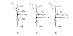
- a Zener diode 9 is connected between the gate terminal 5 of the load drive control element 3 and the ground potential (source potential) 24. Further, the current detection sensor 10 is connected between the drain potential 22 and the ground potential 24. As the current detection sensor 10, for example, as shown in FIG. 2 (a), one using a resistance divided voltage of the resistors 10a and 10b, or as shown in FIGS. 2 (b) and 2 (c), a current detection MOSFET 10c is used. , 10d.
- the temperature detection sensor 11 is connected between the gate terminal 5 and the ground potential 24.
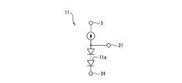
- the temperature detection sensor 11 for example, a sensor using the temperature characteristic of the VF characteristic of the diode 11a shown in FIG. 3 can be used.
- a logic circuit (threshold control circuit) 12 is connected between the gate terminal 5 and the ground potential 24.
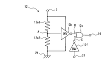
- the logic circuit 12 includes a resistor 12a1, a resistor (or constant current source) 12a2, an inverter (INV) 12b, an OR gate 12c, and an inverter (INV) 12f.
- the output of the temperature detection sensor 11 is input to INV12f, and the outputs of INV12b and INV12f are input to the OR gate 12c. Note that the output of the temperature detection sensor 11 is a voltage that decreases as the temperature rises.
- the voltage at the point A is obtained by dividing the voltage Vin at the gate terminal 5 by the voltage dividing ratio of the resistors 12a1 and 12a2.
- the voltage V1 at the point A is at the H level that is equal to or higher than the threshold voltage Vinv (th) of the INV 12b
- an ED inverter composed of an N-type depletion MOSFET 12d having a source terminal and a gate terminal connected, and an N-type enhancement MOSFET 12e.
- a circuit can be used.
- the N-type depletion MOSFET 12d in which the source terminal and the gate terminal are connected functions as a constant current source.
- the threshold voltage Vinv (th) of the ED inverter is the gate voltage of the N-type enhancement MOSFET 12e when the current flowing through the N-type enhancement MOSFET 12e becomes equal to the constant current I 0 determined by the N-type depletion MOSFET 12d. Since the constant current I 0 does not substantially depend on the power supply voltage and is substantially constant, the threshold voltage Vinv (th) of the ED inverter also has a substantially constant voltage value that does not depend on the power supply voltage.
- a gate resistor 13 is connected between the gate of the power MOSFET 8 and the gate terminal 5. Further, a gate voltage control MOSFET (gate voltage control semiconductor element) 14 is connected between the gate potential 23 and the ground potential 24 of the power MOSFET (insulated gate semiconductor element) 8. The output voltage of the logic circuit 12 is applied to the gate of the gate voltage control MOSFET 14.
- a gate voltage control circuit 15 is connected between the gate potential 23 and the ground potential 24.
- the input terminal of the gate voltage control circuit 15 is connected to the output terminal of the current detection sensor 10.
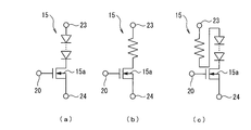
- the gate voltage control circuit 15 one having a configuration as shown in FIGS. 7A to 7C can be used.
- a constant current source 16 is connected between the gate potential 23 and the ground potential 24. The constant current source 16 is for pulling down the gate potential 23 so that the power MOSFET 8 is not erroneously turned on even when noise is applied to the gate terminal 5.
- the load drive control element 3 is destroyed by a large current flowing through the load drive control element 3 when the load 2 is short-circuited. And an overcurrent detection / protection function for preventing the load drive control element 3 from being destroyed by heat generated by the large current.
- the overcurrent detection / protection function is realized by the current detection sensor 10 and the gate voltage control circuit 15.
- the overcurrent detection / protection function will be specifically described below.
- the output of the current detection sensor 10 that is, the voltage of the input 20 of the gate voltage control circuit 15 increases.
- the N-type enhancement MOSFET 15a of the gate voltage control circuit 15 shown in FIG. 7 is turned on. As a result, the gate potential 23 is reduced and the current flowing between the drain terminal 4 and the ground terminal 6 is limited.
- the overheat detection / protection function is realized by the temperature detection sensor 11, the logic circuit 12, and the gate voltage control MOSFET.
- the overheat detection / protection function will be specifically described using an example in which the logical circuit 12 shown in FIG. 6 is applied.
- the output of the temperature detection sensor 11 shown in FIG. 3 that is, the voltage at the input 21 of the logic circuit 12 decreases.
- Vinv (th) of the inverter INV12f the voltage at the point C becomes H level (Vin), and the output of the OR gate 12c also becomes H level ( Vin).
- the voltage Vin is applied from the logic circuit 12 to the gate 19 of the gate voltage control MOSFET 14. Then, the gate voltage control MOSFET 14 is turned on, and the gate potential 23 becomes lower than the threshold voltage of the power MOSFET 8. In this way, the load drive control element 3 is turned off.
- Overcurrent detection / protection function and overheat detection / protection function do not require an external power supply and operate using the voltage at gate terminal 5 as the power supply.
- the load drive control element 3 in this embodiment can operate
- the gate protection circuit is configured externally, but by forming the gate protection circuit in the load drive control element 3, an external element becomes unnecessary. As a result, the cost can be reduced and the occupied area can be reduced. Furthermore, by mounting each detection circuit and gate protection circuit on one chip, the chip cost can be reduced and the assembly process can be simplified.
- the logic circuit 12 and the gate voltage control MOSFET 14 realize a threshold value determining function for determining the threshold voltage (reference voltage) VIN (th) of the load drive control element 3. This function prevents the power MOSFET 8 from being turned on by making the gate potential 23 of the power MOSFET 8 lower than the threshold voltage of the power MOSFET 8 until the voltage of the threshold VIN (th) is applied to the gate terminal 5. is there.
- the threshold voltage Va (th) of the gate voltage control MOSFET 14 is set lower than the threshold voltage Vg (th) of the power MOSFET 8, and the voltage at the gate terminal 5 is set to the threshold voltage Va (of the gate voltage control MOSFET 14).
- the threshold voltage VIN (th) is lower than or equal to th) and lower than the threshold voltage VIN (th)
- the threshold voltage determining function is realized by controlling the gate voltage control MOSFET 14 to be in an ON state.
- the threshold voltage VIN (th) corresponds to the threshold voltage Vinv (th) in FIG.
- VIN (th) Vinv (th) / (voltage division ratio of the resistors 12a1 and 12a2).
- Va (th) ⁇ Vg (th) for example, in the element structure of the gate voltage control MOSFET 14 of FIG.
- a mold layer may be added.
- the concentration of the p-type layer it is conceivable to increase the concentration of the p-type layer.
- Va (th) ⁇ Vg (th) can be achieved by process tuning of each element.
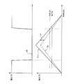
- a timing chart showing the threshold value determining function is as shown in FIG. That is, when the voltage Vin at the gate terminal 5 starts to increase at time t1, the output voltage (gate voltage of the gate voltage control MOSFET 14) Va increases as the voltage Vin at the gate terminal 5 increases. Since the logic circuit 12 uses the voltage of the gate signal as the power supply voltage, the gate voltage Va of the gate voltage control MOSFET 14 is the same as the voltage Vin of the gate terminal 5.
- Va Vin is set so that the gate voltage control MOSFET 14 is kept on, and the power MOSFET 8 is kept off. That is, in the region where the voltage Vin of the gate terminal 5 is lower than the threshold value VIN (th), the output of the logic circuit 12 is set to the H level so that the gate potential 23 (Vg) is always sufficiently lower than the threshold value Vg (th) of the power MOSFET 8.
- the power MOSFET 8 is surely turned off by using a voltage.
- the output of the logic circuit 12 is set to L level, the gate potential 23 (Vg) is set to H level, and the power MOSFET 8 is turned on. Make sure to turn it on.
- the logic circuit 12 can arbitrarily determine the threshold value VIN (th) of the load drive control element 3.
- the gate voltage control MOSFET 14 is turned off, and the voltage Vin of the gate terminal 5 at that time, that is, the power MOSFET 8 is applied to the gate of the power MOSFET 8.
- a voltage sufficiently higher than the threshold value Vg (th) is applied.
- the power MOSFET 8 is turned on and the load drive control element 3 is turned on.
- the gate voltage control MOSFET 14 is turned off, and the voltage Vin of the gate terminal 5 is applied to the gate of the power MOSFET 8.
- the power MOSFET 8 maintains the off state.
- the gate voltage Vg of the power MOSFET 8 also decreases as the voltage Vin at the gate terminal 5 decreases.
- the gate potential 23 (Vg ) can be set to a voltage sufficiently lower than the threshold value Vg (th) of the power MOSFET 8, so that the power MOSFET 8 can be reliably turned off. Further, in a region where the voltage Vin of the gate terminal 5 is equal to or higher than the threshold value VIN (th), the gate potential 23 (Vg) is set to the L level by fixing the output of the logic circuit 12 (if no overheating state is detected). Since it can be set to H level, the power MOSFET 8 can be turned on reliably.
- the threshold value VIN (th) of the load drive control element 3 can be adjusted to an arbitrary voltage.
- the gate voltage Vg (gate potential 123) is determined by the voltage dividing ratio between the resistor 113 and the pull-down resistor 126 as in the conventional insulated gate device driving circuit shown in FIG.
- the method of determining the gate voltage Vg (gate potential 123) is not used, so that the threshold voltage VIN () of the load drive control element 3 does not occur without the voltage drops ⁇ and ⁇ as shown in FIGS. th) can be adjusted.
- the drop of the gate voltage Vg (gate potential 23) with respect to the voltage Vin of the gate terminal 5 does not occur, and the on-resistance of the power MOSFET 8 increases. Can be prevented. Further, as described above, since the pull-down resistor and the diode are not used to realize the threshold value determining function, the chip size can be reduced accordingly.
- the power MOSFET 8 is turned on in a region where the voltage Vin of the gate terminal 5 is lower than the threshold value VIN (th) of the load drive control element 3 (voltage). In a region where Vin is close to Vg (th), rare ON is performed). Therefore, problems such as the occurrence of leakage current occur due to this ON operation.
- Va (th) ⁇ Vg (th) is set, so that the gate potential 23 (Vg) is reached before the gate voltage Va reaches the threshold value Va (th) of the MOSFET 14 for gate voltage control. Can be prevented from reaching the threshold value Vg (th) of the power MOSFET 8. Thereby, the rare ON of the power MOSFET 8 in the region where the voltage Vin of the gate terminal 5 is lower than the threshold value VIN (th) can be eliminated. As a result, it is possible to prevent the occurrence of leakage current due to the rare ON.
- the gate voltage control MOSFET is provided between the gate and the source of the power MOSFET, and the threshold voltage Va (th) of the gate voltage control MOSFET is set lower than the threshold voltage Vg (th) of the power MOSFET. Further, when the gate terminal voltage is lower than the reference voltage higher than the threshold voltage Va (th) of the gate voltage control MOSFET 14 and higher than the threshold voltage Vg (th) of the power MOSFET, the gate voltage control MOSFET is driven to be turned on. To do.
- the power MOSFET can be reliably kept on (if no overheating is detected), and the voltage at the gate terminal is lower than the reference voltage. In, the power MOSFET can be reliably maintained in the off state. Further, since the reference voltage can be arbitrarily adjusted by a logic circuit that drives and controls the gate voltage control MOSFET, the threshold value VIN (th) of the load drive control element can be arbitrarily adjusted.
- the chip size can be reduced accordingly. Furthermore, in a region where the voltage at the gate terminal is higher than the reference voltage, the gate voltage of the power MOSFET can be prevented from dropping with respect to the voltage at the gate terminal, thereby suppressing an increase in the on-resistance of the power MOSFET. can do. As described above, rare ON of the power MOSFET in the region where the voltage of the gate terminal is lower than the reference voltage (threshold VIN (th)) can be prevented, and the occurrence of leakage current due to the rare ON can be prevented.
- the power MOSFET 8 is used as the insulated gate semiconductor element.
- an IGBT insulated gate bipolar transistor
- the constant current source 16 can be omitted.
- the OR gate 12c may be a multi-input, and an abnormality detection signal other than the output of the temperature detection sensor 11 may be input.
- the insulated gate device driving circuit of the present invention it is possible to prevent rare ON of the insulated gate semiconductor element in the region where the voltage value of the gate signal is lower than the reference voltage, and to prevent the occurrence of leakage current. is there. Further, in the region where the voltage value of the gate signal is equal to or higher than the reference voltage, the gate voltage of the insulated gate semiconductor element does not drop with respect to the voltage value of the gate signal, thereby preventing the on-resistance of the insulated gate semiconductor element from increasing. Can be useful.
- SYMBOLS 1 ... Power supply, 2 ... Load, 3 ... Load drive control element, 4 ... Drain terminal, 5 ... Gate terminal, 6 ... Ground terminal (source terminal), 7 ... Ground, 8 ... Power MOSFET (insulated gate semiconductor element), 9 ... Zener diode, 10 ... Current detection sensor, 11 ... Temperature detection sensor, 12 ... Logic circuit (threshold control circuit), 13 ... Gate resistance, 14 ... Gate voltage control MOSFET (gate voltage control semiconductor element), 15 ... Gate Voltage control circuit, 16 ... constant current source, 17 ... drive circuit unit, 18 ... power unit, 19 ... gate voltage control MOSFET gate, 20 ... gate voltage control circuit input, 21 ... logic circuit input, 22 ... drain potential, 23 ... Gate potential, 24 ... Ground potential
Landscapes
- Engineering & Computer Science (AREA)
- Chemical & Material Sciences (AREA)
- Combustion & Propulsion (AREA)
- Mechanical Engineering (AREA)
- General Engineering & Computer Science (AREA)
- Electronic Switches (AREA)
Abstract
デバイスのレアONを防止することができる絶縁ゲート型デバイスの駆動回路を提供する。パワーMOSFET(8)のゲート-ソース間にパワーMOSFET(8)のゲート電圧を下げるためのゲート電圧制御用MOSFET(14)を設け、ゲート電圧制御用MOSFET(14)の閾値電圧Va(th)を、パワーMOSFET(8)の閾値電圧Vg(th)よりも低く設定する。また、ゲート電圧制御用MOSFET(14)は、ゲート端子(5)の電圧Vinがゲート電圧制御用MOSFET(14)の閾値電圧Va(th)以上かつ閾値電圧VIN(th)より低いときには、オン状態に駆動制御される。
Description
本発明は、絶縁ゲート型デバイスの駆動回路に関し、特に当該デバイスのレアオンを防止する絶縁ゲート型デバイスの駆動回路に関する。
図11は、従来の絶縁ゲート型デバイスの駆動回路の構成を示す回路図である。
この図11に示すように、抵抗負荷や誘導負荷等である負荷102の一端は電源101に接続し、負荷102の他端は負荷駆動制御素子(高機能MOSFET)103に接続している。負荷駆動制御素子103は、ドレイン端子104、ゲート端子105、ソース端子106の3端子を有している。ドレイン端子104は負荷102の他端に接続し、ソース端子106はグランドに接続している。また、ゲート端子105には、外部からゲート信号が入力される。負荷駆動制御素子103は、駆動回路部117と、パワー部118とで構成されており、駆動回路部117とパワー部118とは1つの半導体チップ内に形成する。
この図11に示すように、抵抗負荷や誘導負荷等である負荷102の一端は電源101に接続し、負荷102の他端は負荷駆動制御素子(高機能MOSFET)103に接続している。負荷駆動制御素子103は、ドレイン端子104、ゲート端子105、ソース端子106の3端子を有している。ドレイン端子104は負荷102の他端に接続し、ソース端子106はグランドに接続している。また、ゲート端子105には、外部からゲート信号が入力される。負荷駆動制御素子103は、駆動回路部117と、パワー部118とで構成されており、駆動回路部117とパワー部118とは1つの半導体チップ内に形成する。
パワー部118は、パワーMOSFET108からなる。パワーMOSFET108は、駆動回路部117によってオンオフ制御される絶縁ゲート型デバイスである。
負荷駆動制御素子103のゲート端子105およびパワーMOSFET108のゲート電位123とグランド電位(ソース電位)124との間には、温度を検出する温度検出センサ111と、温度検出センサ111の信号処理を行う論理回路112と、論理回路112の信号を受けてゲート電位123のシャットダウンを制御するゲート電圧制御用MOSFET114とをそれぞれ設ける。
負荷駆動制御素子103のゲート端子105およびパワーMOSFET108のゲート電位123とグランド電位(ソース電位)124との間には、温度を検出する温度検出センサ111と、温度検出センサ111の信号処理を行う論理回路112と、論理回路112の信号を受けてゲート電位123のシャットダウンを制御するゲート電圧制御用MOSFET114とをそれぞれ設ける。
また、ドレイン電位122とグランド電位(ソース電位)124との間には、電流検出センサ110を設けており、ゲート電位123とグランド電位(ソース電位)124との間には、電流検出センサ110の信号を受けてゲート電位123の電圧レベルを制御するゲート電圧制御回路115も設ける。
その他にゲート電位123とグランド電位(ソース電位)124との間には、ダイオード109、入力抵抗113及びダイオード125を設ける。ダイオード109と入力抵抗113の接続点はゲート端子105に接続する。また、ゲート電位123とグランド電位(ソース電位)124との間には、ゲート端子105にノイズが来てもパワーMOSFET108が誤オンしないようにゲート電位123をプルダウンするための定電流源116を設ける。さらに、ゲート電位123とグランド電位(ソース電位)124との間には、プルダウン抵抗126を設ける。
負荷駆動制御素子103は、負荷102を駆動するためのスイッチング素子として機能する。また、この負荷駆動制御素子103は、上記スイッチング機能以外に、負荷102が短絡したとき等に負荷駆動制御素子103に流れる大電流により負荷駆動制御素子103自体が破壊するのを防止するための過電流検出機能、その大電流による発熱で負荷駆動制御素子103自体が破壊するのを防止するための過熱検出機能、およびスイッチング素子のゲート保護機能を有する。過熱検出機能及び過電流検出機能は、ゲート電圧を電源として動作する。
過熱検出機能は以下のように動作する。すなわち、温度上昇に伴い温度検出センサ111の出力(論理回路112の入力)121の電圧が所定の電圧に達したとき、論理回路112は、ゲート電圧制御用MOSFET114のゲート119に電圧制御用MOSFET114をオン状態とする電圧を印加する。これにより、ゲート電位123をパワーMOSFET108の閾値電圧より低くしてパワーMOSFET108をオフし、負荷駆動制御素子103をオフする。
また、過電流検出機能は以下のように動作する。すなわち、ドレイン端子104とグランド端子(ソース端子)106との間に流れる電流の増大に伴い、電流検出センサ110からゲート電圧制御回路115への入力120が所定の電圧に達したとき、ゲート電圧制御回路115は、ゲート電位123を小さくすることにより、ドレイン端子104とグランド端子(ソース端子)106との間に流れる電流を制限する。
そして、入力抵抗113、ダイオード125及びプルダウン抵抗126は、負荷駆動制御素子103の閾値VIN(th)を決定する閾値決定機能も有している。
図12は、閾値決定機能の一例を示すタイミングチャートである。ここでは、ゲート端子105に三角波が入力された場合のゲート端子105の電圧Vin、パワーMOSFET108のゲート電圧Vg(ゲート電位123)、ドレイン電圧Vd(ドレイン電位122)を示している。
図12は、閾値決定機能の一例を示すタイミングチャートである。ここでは、ゲート端子105に三角波が入力された場合のゲート端子105の電圧Vin、パワーMOSFET108のゲート電圧Vg(ゲート電位123)、ドレイン電圧Vd(ドレイン電位122)を示している。
この図12は、図11のゲート端子105の電圧Vinを、入力抵抗113とプルダウン抵抗126との分圧比で分圧してゲート電圧Vg(ゲート電位123)を決定する場合について示している。すなわち、ここでは、入力抵抗113とプルダウン抵抗126との分圧比によりゲート電圧Vg(ゲート電位123)を調整することで、ゲート電圧Vg(ゲート電位123)がパワーMOSFET108の閾値電圧Vg(th)以上となるタイミングを調整している。このようにして、負荷駆動制御素子103の閾値VIN(th)を調整する。
また、プルダウン抵抗126のチップ上でのレイアウトサイズが大きくなりすぎる等の場合には、プルダウン抵抗126を削除し、ダイオード125と定電流源116と入力抵抗113とでゲート電圧Vg(ゲート電位123)を調整する。すなわち、ゲート端子105の電圧Vinをβ=(ダイオード125の順電圧(Vf)+入力抵抗113の抵抗値×定電流源116の電流値)分ドロップさせてゲート電圧Vg(ゲート電位123)を決定することで、負荷駆動制御素子103の閾値VIN(th)を調整する。なお、(入力抵抗113の抵抗値×定電流源116の電流値)の項は小さな値となるので、実質はβ=ダイオード125の順電圧(Vf)となる。この場合、タイミングチャートは図13に示すようになる。
また、パワーMOSFETがターンオフする際に発生するサージ電圧とターンオフ損失とを効果的に低減するものとしては、例えば特許文献1に記載の技術がある。この技術は、パワーMOSFETの主端子に流れる電流をターンオフする際にゲート容量を放電させる電流源回路と、この電流源回路を介してゲート容量を放電する電流値を調整する電流調整回路とを備えるものである。
この特許文献1に記載の技術では、ゲート信号によりパワーMOSFETがターンオフするときに電流源回路を接続し、パワーMOSFETがターンオンしているときは電流源回路を切り離すようにしている。また、ここでは、電流源回路の出力電流を可変とし、電流調整回路により、パワーMOSFETの主端子両端の電圧が上昇をはじめるまでは電流源回路の出力電流を一定値とし、上記主端子両端の電圧の上昇に伴って電流源回路の出力電流を徐々に低下させている。
さらに、並列接続の可制御半導体素子の主電流をバランスさせるものとしては、例えば特許文献2に記載の技術がある。この技術は、並列接続の可制御半導体素子の電流を検出し、この電流検出信号が等しくなるように各並列スイッチング素子のゲート電圧を制御するものである。
ところで、上述した図11に示す絶縁ゲート型デバイスの駆動回路では、図12及び図13に示すように負荷駆動制御素子103の閾値VIN(th)を任意の電圧に調整可能である。しかしながら、この場合、図12のα及び図13のβに示すように、ゲート端子105の電圧Vinに比べ、パワーMOSFET108のゲート電圧Vg(ゲート電位123)がドロップしてしまうため、パワーMOSFET108のオン抵抗が高くなってしまう。
図13のβに示すように、ダイオード125を用いて閾値VIN(th)を調整する構成とすれば、上記電圧ドロップを、ゲート端子105の電圧Vinの大きさによらず一定とすることができる。そのため、プルダウン抵抗126を用いて閾値VIN(th)を調整する構成する場合(図12のα)と比較して、パワーMOSFET108のオン抵抗の増大に歯止めをかけることができる。しかしながら、電圧ドロップが発生しないようにすることはできないため、パワーMOSFET108のオン抵抗が高くなるのを防止することはできない。
また、この場合、ゲート電圧Vg(ゲート電位123)がパワーMOSFET108の閾値Vg(th)に近づいたときに、パワーMOSFET108が完全にオン状態になる前にわずかにオン状態になる、所謂レアON状態となって、リーク電流が発生するおそれがある。
しかしながら、上記各特許文献に記載の技術では、パワーMOSFETのレアON対策が講じられておらず、パワーMOSFETがレアON状態になることに起因するリーク電流の発生を確実に回避することができない。
そこで、本発明は、デバイスのレアONを防止することができる絶縁ゲート型デバイスの駆動回路を提供することを課題としている。
しかしながら、上記各特許文献に記載の技術では、パワーMOSFETのレアON対策が講じられておらず、パワーMOSFETがレアON状態になることに起因するリーク電流の発生を確実に回避することができない。
そこで、本発明は、デバイスのレアONを防止することができる絶縁ゲート型デバイスの駆動回路を提供することを課題としている。
上記課題を解決するために、本発明の第1の態様は、絶縁ゲート半導体素子のゲート-ソース間に接続し、外部から入力されるゲート信号によって駆動されるゲート電圧制御用半導体素子を備え、前記ゲート電圧制御用半導体素子の閾値電圧は、前記絶縁ゲート半導体素子の閾値電圧よりも低く設定されており、前記ゲート信号の電圧値が、前記ゲート電圧制御用半導体素子の閾値電圧以上かつ前記絶縁ゲート半導体素子の閾値電圧よりも高い所定の基準電圧より低いとき、前記ゲート電圧制御用半導体素子をオン状態に駆動制御することを特徴としている。
このように、ゲート電圧制御用半導体素子の閾値電圧を絶縁ゲート半導体素子の閾値電圧よりも低く設定すると共に、ゲート信号の電圧値がゲート電圧制御用半導体素子の閾値電圧以上かつ基準電圧より低いときには、ゲート電圧制御用半導体素子をオン状態に駆動制御する。これにより、ゲート信号の電圧値が上昇する過程において、ゲート信号の電圧値がゲート電圧制御用半導体素子の閾値電圧に達した後に、絶縁ゲート半導体素子の閾値電圧に達するようにすることができる。
したがって、ゲート信号の電圧値が基準電圧に達するまでの間、確実に絶縁ゲート半導体素子をオフ状態とすることができる。すなわち、ゲート信号の電圧値が基準電圧に達してから初めて絶縁ゲート半導体素子のゲートに閾値以上の電圧を印加する。これにより、ゲート信号の電圧値が基準電圧より低い領域における絶縁ゲート半導体素子のレアONを防ぎ、リーク電流の発生を抑制することができる。
また、本発明の第2の態様は、前記ゲート電圧制御用半導体素子を駆動制御する閾値制御回路を備え、前記閾値制御回路の前記基準電圧を任意に設定可能であってもよい。
これにより、絶縁ゲート半導体素子がターンオンする電圧値を任意に調整することが可能である。
また、本発明の第2の態様は、前記ゲート電圧制御用半導体素子を駆動制御する閾値制御回路を備え、前記閾値制御回路の前記基準電圧を任意に設定可能であってもよい。
これにより、絶縁ゲート半導体素子がターンオンする電圧値を任意に調整することが可能である。
本発明によれば、ゲート電圧制御用半導体素子の閾値電圧を絶縁ゲート半導体素子の閾値電圧よりも低く設定すると共に、ゲート信号の電圧値がゲート電圧制御用半導体素子の閾値電圧以上かつ基準電圧より低いときには、ゲート電圧制御用半導体素子をオン状態に駆動制御するので、ゲート信号の電圧値が基準電圧より低い領域における絶縁ゲート半導体素子のレアONを防ぎ、リーク電流の発生を防止することができる。
また、ゲート信号の電圧値が基準電圧以上である領域においては、ゲート信号の電圧値に対する絶縁ゲート半導体素子のゲート電圧のドロップが発生しないため、絶縁ゲート半導体素子のオン抵抗が高くなるのを防止することができる。
また、ゲート信号の電圧値が基準電圧以上である領域においては、ゲート信号の電圧値に対する絶縁ゲート半導体素子のゲート電圧のドロップが発生しないため、絶縁ゲート半導体素子のオン抵抗が高くなるのを防止することができる。
以下、本発明の実施の形態を図面に基づいて説明する。
(第1の実施形態)
(構成)
図1は、本実施形態における絶縁ゲート型デバイスの駆動回路を適用した半導体集積回路装置の構成を示す回路図である。
この図1に示すように、抵抗負荷や誘導負荷等の負荷2の一端は電源1に接続し、負荷2の他端は半導体集積回路装置である負荷駆動制御素子3に接続している。
(第1の実施形態)
(構成)
図1は、本実施形態における絶縁ゲート型デバイスの駆動回路を適用した半導体集積回路装置の構成を示す回路図である。
この図1に示すように、抵抗負荷や誘導負荷等の負荷2の一端は電源1に接続し、負荷2の他端は半導体集積回路装置である負荷駆動制御素子3に接続している。
負荷駆動制御素子3は、ドレイン端子4、ゲート端子5、ソース端子6の3端子を有している。ドレイン端子4は負荷2の他端に接続し、ソース端子6はグランドに接続する。また、ゲート端子5には、外部からゲート信号が入力される。負荷駆動制御素子3は、駆動回路部17とパワー部18とで構成されており、これらは1つの半導体チップ内に形成されている。パワー部18は、駆動回路部17によってオンオフ制御されるパワーMOSFET(絶縁ゲート半導体素子)8からなる。
負荷駆動制御素子3のゲート端子5とグランド電位(ソース電位)24との間には、ツェナーダイオード9を接続する。
また、ドレイン電位22とグランド電位24との間には、電流検出センサ10を接続する。電流検出センサ10としては、例えば、図2(a)に示すように、抵抗10a及び10bの抵抗分圧を用いたものや、図2(b),(c)に示すように、電流検出MOSFET10c,10dを用いたものがある。
また、ドレイン電位22とグランド電位24との間には、電流検出センサ10を接続する。電流検出センサ10としては、例えば、図2(a)に示すように、抵抗10a及び10bの抵抗分圧を用いたものや、図2(b),(c)に示すように、電流検出MOSFET10c,10dを用いたものがある。
さらに、ゲート端子5とグランド電位24との間には、温度検出センサ11を接続する。温度検出センサ11としては、例えば、図3に示すダイオード11aのVF特性の温度特性を利用したセンサを用いることができる。
また、ゲート端子5とグランド電位24との間には、論理回路(閾値制御回路)12を接続する。論理回路12としては、例えば、図4に示すように、抵抗12a1と、抵抗(又は定電流源)12a2と、インバータ(INV)12bと、ORゲート12cと、インバータ(INV)12fとから構成される回路を用いることができる。ここで、INV12fには温度検出センサ11の出力が入力され、ORゲート12cにはINV12b,INV12fの出力が入力されるようになっている。なお、温度検出センサ11の出力は、温度上昇に伴って小さくなる電圧である。
また、ゲート端子5とグランド電位24との間には、論理回路(閾値制御回路)12を接続する。論理回路12としては、例えば、図4に示すように、抵抗12a1と、抵抗(又は定電流源)12a2と、インバータ(INV)12bと、ORゲート12cと、インバータ(INV)12fとから構成される回路を用いることができる。ここで、INV12fには温度検出センサ11の出力が入力され、ORゲート12cにはINV12b,INV12fの出力が入力されるようになっている。なお、温度検出センサ11の出力は、温度上昇に伴って小さくなる電圧である。
図4に示す構成により、点Aの電圧は、ゲート端子5の電圧Vinを抵抗12a1,12a2の分圧比で分圧したものとなる。図5に示すように、点Aの電圧V1がINV12bの閾値電圧Vinv(th)を下回っているLレベルであるとき、点Bの電圧V2はHレベルとなる(V2=Vin)。そして、点Aの電圧V1がINV12bの閾値電圧Vinv(th)以上となるHレベルであるとき、点Bの電圧V2はLレベルとなる(V2=0)。
さらに、論理回路12のインバータINV12b,INV12fとしては、例えば、図6に示すように、ソース端子とゲート端子とが接続されたN型デプレッションMOSFET12dと、N型エンハンスメントMOSFET12eとから構成されるED型インバータ回路を用いることができる。ここで、ソース端子とゲート端子とが接続されたN型デプレッションMOSFET12dは、定電流源として機能するものである。
図4,図6に示す構成により、点Aの電圧に対するインバータINV12bの動作は以下のようになる。すなわち、点Aに、図5に示すような電圧Vinの分圧電圧V1が入力されると、この点Aの電圧V1がED型インバータの閾値電圧Vinv(th)を下回っているLレベルであるとき、N型エンハンスメントMOSFET12eはオフとなり、点Bの電圧V2はHレベルとなる(V2=Vin)。そして、点Aの電圧V1がED型インバータの閾値電圧Vinv(th)以上となるHレベルとなると、N型エンハンスメントMOSFET12eはオンとなり、点Bの電圧V2はLレベルとなる(V2=0)。温度検出センサ11の出力電圧21に対するインバータINV12fの動作も、これと同様である。
なお、ED型インバータの閾値電圧Vinv(th)は、N型エンハンスメントMOSFET12eに流れる電流が、N型デプレッションMOSFET12dにより定まる定電流I0と等しくなるときのN型エンハンスメントMOSFET12eのゲート電圧である。定電流I0は電源電圧に殆ど依存せず略一定であるため、ED型インバータの閾値電圧Vinv(th)も電源電圧によらない略一定の電圧値となる。
図1に戻って、パワーMOSFET8のゲートとゲート端子5の間には、ゲート抵抗13が接続されている。
さらに、パワーMOSFET(絶縁ゲート半導体素子)8のゲート電位23とグランド電位24との間には、ゲート電圧制御用MOSFET(ゲート電圧制御用半導体素子)14が接続されている。ゲート電圧制御用MOSFET14のゲートには、論理回路12の出力電圧が印加される。
さらに、パワーMOSFET(絶縁ゲート半導体素子)8のゲート電位23とグランド電位24との間には、ゲート電圧制御用MOSFET(ゲート電圧制御用半導体素子)14が接続されている。ゲート電圧制御用MOSFET14のゲートには、論理回路12の出力電圧が印加される。
また、ゲート電位23とグランド電位24との間には、ゲート電圧制御回路15が接続されている。このゲート電圧制御回路15の入力端は、電流検出センサ10の出力端に接続している。ゲート電圧制御回路15としては、図7(a)~(c)に示すような構成のものを用いることができる。
さらに、ゲート電位23とグランド電位24との間には、定電流源16が接続されている。この定電流源16は、ゲート端子5にノイズが来てもパワーMOSFET8が誤オンしないようにゲート電位23をプルダウンするためのものである。
さらに、ゲート電位23とグランド電位24との間には、定電流源16が接続されている。この定電流源16は、ゲート端子5にノイズが来てもパワーMOSFET8が誤オンしないようにゲート電位23をプルダウンするためのものである。
この負荷駆動制御素子3は、負荷2を駆動するためのスイッチング素子としての機能の他に、負荷2が短絡したとき等に負荷駆動制御素子3に流れる大電流により負荷駆動制御素子3自体が破壊するのを防止するための過電流検出・保護機能と、その大電流による発熱で負荷駆動制御素子3自体が破壊するのを防止するための過熱検出・保護機能とを有する。
過電流検出・保護機能は、電流検出センサ10およびゲート電圧制御回路15で実現する。以下、過電流検出・保護機能について具体的に説明する。
ドレイン端子4とグランド端子6との間に過電流が流れると、電流検出センサ10の出力、すなわちゲート電圧制御回路15の入力20の電圧は大きくなる。ゲート電圧制御回路15の入力20の電圧が所定電圧以上となると、図7に示すゲート電圧制御回路15のN型エンハンスメントMOSFET15aがオンする。これにより、ゲート電位23を小さくし、ドレイン端子4とグランド端子6との間に流れる電流を制限する。
ドレイン端子4とグランド端子6との間に過電流が流れると、電流検出センサ10の出力、すなわちゲート電圧制御回路15の入力20の電圧は大きくなる。ゲート電圧制御回路15の入力20の電圧が所定電圧以上となると、図7に示すゲート電圧制御回路15のN型エンハンスメントMOSFET15aがオンする。これにより、ゲート電位23を小さくし、ドレイン端子4とグランド端子6との間に流れる電流を制限する。
過熱検出・保護機能は、温度検出センサ11、論理回路12およびゲート電圧制御用MOSFET14で実現する。以下、過熱検出・保護機能について、図6に示す論路回路12を適用した例を用いて具体的に説明する。
温度上昇に伴い、図3に示す温度検出センサ11の出力、すなわち論理回路12の入力21の電圧は小さくなる。このとき、図6に示す論理回路12の入力21の電圧がインバータINV12fの閾値電圧Vinv(th)以下となると、点Cの電圧がHレベル(Vin)となり、ORゲート12cの出力もHレベル(Vin)となる。これにより、論理回路12からゲート電圧制御用MOSFET14のゲート19に電圧Vinを印加する。すると、ゲート電圧制御用MOSFET14がオンし、ゲート電位23がパワーMOSFET8の閾値電圧より低くなる。このようにして負荷駆動制御素子3をオフする。
温度上昇に伴い、図3に示す温度検出センサ11の出力、すなわち論理回路12の入力21の電圧は小さくなる。このとき、図6に示す論理回路12の入力21の電圧がインバータINV12fの閾値電圧Vinv(th)以下となると、点Cの電圧がHレベル(Vin)となり、ORゲート12cの出力もHレベル(Vin)となる。これにより、論理回路12からゲート電圧制御用MOSFET14のゲート19に電圧Vinを印加する。すると、ゲート電圧制御用MOSFET14がオンし、ゲート電位23がパワーMOSFET8の閾値電圧より低くなる。このようにして負荷駆動制御素子3をオフする。
過電流検出・保護機能および過熱検出・保護機能は、外部電源を必要とせず、ゲート端子5の電圧を電源として動作する。これにより、本実施形態における負荷駆動制御素子3は、単体MOSFET同様、3端子で動作することができる。また、ゲート保護回路は外付けで構成されるのが一般的であるが、これを負荷駆動制御素子3内に形成することで、外付け素子が不要となる。その結果、コストダウン、占有面積の縮小化が可能となる。さらに、各検出回路及びゲート保護回路を1チップに搭載することによるチップコストの低減、組立工程の簡略化が可能になる。
また、論理回路12及びゲート電圧制御用MOSFET14で、負荷駆動制御素子3の閾値電圧(基準電圧)VIN(th)を決定する閾値決定機能を実現する。この機能は、ゲート端子5に閾値VIN(th)の電圧が印加されるまでは、パワーMOSFET8のゲート電位23をパワーMOSFET8の閾値電圧よりも低くして、パワーMOSFET8をオンしないようにするものである。
本実施形態では、ゲート電圧制御用MOSFET14の閾値電圧Va(th)をパワーMOSFET8の閾値電圧Vg(th)よりも低く設定すると共に、ゲート端子5の電圧がゲート電圧制御用MOSFET14の閾値電圧Va(th)以上かつ閾値電圧VIN(th)より低いときには、ゲート電圧制御用MOSFET14をオン状態に駆動制御することで、上記閾値決定機能を実現する。なお、上記閾値電圧VIN(th)は、図5における閾値電圧Vinv(th)に対応している。ここで、VIN(th)=Vinv(th)/(抵抗12a1,12a2の分圧比)である。
Va(th)<Vg(th)の関係を達成するためには、例えば図8のゲート電圧制御用MOSFET14の素子構造において、p型の拡散層を低濃度とする、チャネル領域に低濃度のn型層を追加する等が考えられる。また、図8のパワーMOSFET8の素子構造においては、p型層を高濃度とする等が考えられる。このように、各素子のプロセスチューニングによりVa(th)<Vg(th)の達成が可能である。なお、Va(th)<Vg(th)の達成方法については上記の他にも様々な方法があり、適宜選択可能である。
ゲート端子5にゲート信号として三角波が入力された場合、閾値決定機能を示すタイミングチャートは図9に示すようになる。すなわち、時刻t1で、ゲート端子5の電圧Vinが上昇し始めると、ゲート端子5の電圧Vinの上昇に伴って論理回路12の出力電圧(ゲート電圧制御用MOSFET14のゲート電圧)Vaが上昇する。論理回路12は、電源電圧としてゲート信号の電圧を利用しているため、ゲート電圧制御用MOSFET14のゲート電圧Vaはゲート端子5の電圧Vinと同じになる。
また、時刻t2でゲート電圧制御用MOSFET14のゲート電圧Vaがゲート電圧制御用MOSFET14の閾値Va(th)に達するまでは、ゲート電圧制御用MOSFET14がオフしているので、パワーMOSFET8のゲート電位23(Vg)はゲート端子5の電圧Vinに等しい(Vg=Vin)。
その後、時刻t2で、ゲート電圧制御用MOSFET14のゲート電圧Vaがゲート電圧制御用MOSFET14の閾値Va(th)に達すると、ゲート電圧制御用MOSFET14がオンする。したがって、パワーMOSFET8のゲート電位23(Vg)は接地電圧(0[V])となる。
その後、時刻t2で、ゲート電圧制御用MOSFET14のゲート電圧Vaがゲート電圧制御用MOSFET14の閾値Va(th)に達すると、ゲート電圧制御用MOSFET14がオンする。したがって、パワーMOSFET8のゲート電位23(Vg)は接地電圧(0[V])となる。
そして、時刻t3で、ゲート端子5の電圧Vinが負荷駆動制御素子3の閾値VIN(th)に達すると、論理回路12がオフ信号(Va=0)を出力することによりゲート電圧制御用MOSFET14がオフする。これにより、パワーMOSFET8のゲートにゲート端子5の電圧Vinが印加される。このように、ゲート電圧制御用MOSFET14は、ゲート端子5の電圧Vinがゲート電圧制御用MOSFET14の閾値電圧Va(th)以上かつ閾値VIN(th)より低いときにオン状態に駆動制御される。
この時刻t3では、パワーMOSFET8のゲート電位23(Vg)がパワーMOSFET8の閾値Vg(th)を超えているため、この時点でパワーMOSFET8がオフ状態からオン状態に完全に切り替わり、負荷駆動制御素子3がオン状態となる。
このように、Va(th)<Vg(th)とすることにより、ゲート電位23(Vg)がパワーMOSFET8の閾値電圧Vg(th)を超える前に、ゲート電圧制御用MOSFET14のゲート電圧Vaを閾値Va(th)に到達させ、ゲート電圧制御用MOSFET14をオンしてパワーMOSFET8をオフするようにする。
このように、Va(th)<Vg(th)とすることにより、ゲート電位23(Vg)がパワーMOSFET8の閾値電圧Vg(th)を超える前に、ゲート電圧制御用MOSFET14のゲート電圧Vaを閾値Va(th)に到達させ、ゲート電圧制御用MOSFET14をオンしてパワーMOSFET8をオフするようにする。
そして、その後は、ゲート端子5の電圧Vinが閾値VIN(th)に達するまで、ゲート電圧制御用MOSFET14がオン状態を維持するようにVa=Vinとし、パワーMOSFET8をオフ状態に維持する。すなわち、ゲート端子5の電圧Vinが閾値VIN(th)より低い領域では論理回路12の出力をHレベルとすることで、ゲート電位23(Vg)を必ずパワーMOSFET8の閾値Vg(th)より充分低い電圧にして、パワーMOSFET8を確実にオフするようにする。
また、ゲート端子5の電圧Vinが閾値VIN(th)以上の領域では、過熱状態が検出されていなければ論理回路12の出力をLレベルとしてゲート電位23(Vg)をHレベルとし、パワーMOSFET8を確実にオンするようにする。
このとき、論理回路12がオフ信号(Va=0)を出力するタイミングを制御する(図4に示す論理回路12の構成例では、抵抗12a1,12a2の分圧比やインバータINV12bの閾値電圧Vinv(th)を調整することでこれを実現する。)ことで、ゲート電位23(Vg)をLレベルからHレベルへ切り替えるタイミングを制御することができる。換言すると、論理回路12が負荷駆動制御素子3の閾値VIN(th)を任意に決定可能な構成となっている。
このとき、論理回路12がオフ信号(Va=0)を出力するタイミングを制御する(図4に示す論理回路12の構成例では、抵抗12a1,12a2の分圧比やインバータINV12bの閾値電圧Vinv(th)を調整することでこれを実現する。)ことで、ゲート電位23(Vg)をLレベルからHレベルへ切り替えるタイミングを制御することができる。換言すると、論理回路12が負荷駆動制御素子3の閾値VIN(th)を任意に決定可能な構成となっている。
(動作)
次に、本実施形態の動作について説明する。
今、負荷駆動制御素子3をオン状態とするべく、外部から負荷駆動制御素子3のゲート端子5にゲート信号を入力したものとする。このとき、図9に示すように、ゲート信号として三角波を入力したものとすると、上述した閾値決定機能により、時刻t3でゲート端子5の電圧が負荷駆動制御素子3の閾値VIN(th)に達するまで、ゲート電位23(Vg)はパワーMOSFET8の閾値電圧より低くなる。そのため、パワーMOSFET8は、時刻t3までオフ状態を維持する。その後、時刻t3で、ゲート端子5の電圧Vinが閾値VIN(th)に達すると、ゲート電圧制御用MOSFET14がオフし、パワーMOSFET8のゲートにその時点でのゲート端子5の電圧Vin、すなわちパワーMOSFET8の閾値Vg(th)より充分高い電圧が印加される。これにより、パワーMOSFET8がオンし、負荷駆動制御素子3がオン状態となる。
次に、本実施形態の動作について説明する。
今、負荷駆動制御素子3をオン状態とするべく、外部から負荷駆動制御素子3のゲート端子5にゲート信号を入力したものとする。このとき、図9に示すように、ゲート信号として三角波を入力したものとすると、上述した閾値決定機能により、時刻t3でゲート端子5の電圧が負荷駆動制御素子3の閾値VIN(th)に達するまで、ゲート電位23(Vg)はパワーMOSFET8の閾値電圧より低くなる。そのため、パワーMOSFET8は、時刻t3までオフ状態を維持する。その後、時刻t3で、ゲート端子5の電圧Vinが閾値VIN(th)に達すると、ゲート電圧制御用MOSFET14がオフし、パワーMOSFET8のゲートにその時点でのゲート端子5の電圧Vin、すなわちパワーMOSFET8の閾値Vg(th)より充分高い電圧が印加される。これにより、パワーMOSFET8がオンし、負荷駆動制御素子3がオン状態となる。
負荷駆動制御素子3をオン状態からオフ状態へ切り替える場合には、負荷駆動制御素子3のゲート端子5にオフ信号を入力する。すなわち、図9の時刻t4以降、ゲート端子5の電圧Vinは低下する。すると、これに伴いパワーMOSFET8のゲート電圧Vgが低下する。そして、時刻t5でゲート端子5の電圧Vinが閾値VIN(th)より低くなると、ゲート電圧制御用MOSFET14のゲートに、その時点でのゲート端子5の電圧Vinが印加される。このときゲート端子5の電圧Vinは、ゲート電圧制御用MOSFET14の閾値Va(th)以上となっているため、この時刻t5でゲート電圧制御用MOSFET14がオンする。これにより、パワーMOSFET8のゲート電圧Vgが接地電圧となってパワーMOSFET8が速やかにオフし、負荷駆動制御素子3がオフ状態となる。
その後、時刻t6でゲート端子5の電圧Vinがゲート電圧制御用MOSFET14の閾値Va(th)より低くなると、ゲート電圧制御用MOSFET14がオフし、パワーMOSFET8のゲートにゲート端子5の電圧Vinが印加される。このとき、パワーMOSFET5のゲート電圧VgはパワーMOSFET8の閾値Vg(th)を充分下回っていることから、パワーMOSFET8はオフ状態を維持する。そして、時刻t6以降は、ゲート端子5の電圧Vinの低下に伴って、パワーMOSFET8のゲート電圧Vgも低下していく。
このように、Va(th)<Vg(th)とし、ゲート端子5の電圧Vinが閾値VIN(th)より低い領域で論理回路12の出力をHレベル固定とすることで、ゲート電位23(Vg)をパワーMOSFET8の閾値Vg(th)より充分低い電圧にすることができるので、パワーMOSFET8を確実にオフすることができる。また、ゲート端子5の電圧Vinが閾値VIN(th)以上の領域では、(過熱状態が検出されていなければ)論理回路12の出力をLレベル固定とすることで、ゲート電位23(Vg)をHレベルとすることができるので、パワーMOSFET8を確実にオンすることができる。
また、論理回路12がLレベルの出力(オフ信号)を出力するタイミングを調整することで(図4に示す論理回路12の構成例では、抵抗12a1,12a2の分圧比やインバータINV12bの閾値電圧Vinv(th)を調整することで)、負荷駆動制御素子3の閾値VIN(th)を任意の電圧に調整することができる。
さらに、図11に示す従来の絶縁ゲート型デバイスの駆動回路のような、抵抗113とプルダウン抵抗126との分圧比によりゲート電圧Vg(ゲート電位123)を決定したり、ダイオード125による電圧降下を利用してゲート電圧Vg(ゲート電位123)を決定したりする手法を用いないので、図12及び図13に示されるような電圧ドロップα及びβが発生することなく負荷駆動制御素子3の閾値VIN(th)を調整可能である。
そのため、ゲート端子5の電圧Vinが閾値VIN(th)以上の領域において、ゲート端子5の電圧Vinに対するゲート電圧Vg(ゲート電位23)のドロップが発生せず、パワーMOSFET8のオン抵抗が高くなるのを防止することができる。また、上述したように閾値決定機能の実現にプルダウン抵抗やダイオードを用いないため、その分のチップサイズの削減が可能となる。
ところで、図1と同様の回路構成において、本実施形態のようにVa(th)<Vg(th)としない場合、即ちVa(th)>Vg(th)とした場合の動作波形図は、図10に示すようになる。
ここではVa(th)>Vg(th)に設定しているため、時刻t11でゲート端子5の電圧Vinが上昇し始め、それに伴ってゲート電圧制御用MOSFET14のゲート電圧VaとパワーMOSFET8のゲート電位23(Vg)とが上昇した場合、ゲート電圧Vaがゲート電圧制御用MOSFET14の閾値Va(th)に達する前に、時刻t12でゲート電位23(Vg)がパワーMOSFET8の閾値Vg(th)に達してしまう。
ここではVa(th)>Vg(th)に設定しているため、時刻t11でゲート端子5の電圧Vinが上昇し始め、それに伴ってゲート電圧制御用MOSFET14のゲート電圧VaとパワーMOSFET8のゲート電位23(Vg)とが上昇した場合、ゲート電圧Vaがゲート電圧制御用MOSFET14の閾値Va(th)に達する前に、時刻t12でゲート電位23(Vg)がパワーMOSFET8の閾値Vg(th)に達してしまう。
すなわち、時刻t11から時刻t12までの間は、ゲート電位23(Vg)が閾値Vg(th)以下であるためパワーMOSFET8はオフ状態であるが、時刻t12から時刻t13までの間は、ゲート電圧Va(=Vin)が閾値Va(th)に達しておらず、且つゲート電位23(Vg)が閾値Vg(th)に達しているため、パワーMOSFET8はオン状態となってしまう。
そして、時刻t13でゲート電圧Va(=Vin)が閾値Va(th)に達すると、ゲート電圧制御用MOSFET14がオン状態となって、パワーMOSFET8はオフ状態に切り替わる。その後は、時刻t14でゲート端子5の電圧Vinが負荷駆動制御素子3の閾値VIN(th)に達してゲート電圧制御用MOSFET14がオフ状態となるまで、パワーMOSFET8はオフ状態を維持する。
このように、Va(th)>Vg(th)に設定した場合、ゲート端子5の電圧Vinが負荷駆動制御素子3の閾値VIN(th)より低い領域で、パワーMOSFET8がオンしてしまう(電圧VinがVg(th)に近い領域ではレアONとなる)。そのため、このON動作によりリーク電流が発生するなどの問題が生じる。
これに対して、本実施形態では、Va(th)<Vg(th)に設定するので、ゲート電圧Vaがゲート電圧制御用MOSFET14の閾値Va(th)に達する前に、ゲート電位23(Vg)がパワーMOSFET8の閾値Vg(th)に達するのを防止することができる。これにより、ゲート端子5の電圧Vinが閾値VIN(th)より低い領域における、パワーMOSFET8のレアONを解消することができる。その結果、当該レアONに起因するリーク電流の発生を防止することができる。
(効果)
上記実施形態では、パワーMOSFETのゲート-ソース間にゲート電圧制御用MOSFETを設け、ゲート電圧制御用MOSFETの閾値電圧Va(th)を、パワーMOSFETの閾値電圧Vg(th)よりも低く設定する。また、ゲート端子の電圧がゲート電圧制御用MOSFET14の閾値電圧Va(th)以上かつパワーMOSFETの閾値電圧Vg(th)よりも高い基準電圧より低いときには、ゲート電圧制御用MOSFETをオン状態に駆動制御する。
上記実施形態では、パワーMOSFETのゲート-ソース間にゲート電圧制御用MOSFETを設け、ゲート電圧制御用MOSFETの閾値電圧Va(th)を、パワーMOSFETの閾値電圧Vg(th)よりも低く設定する。また、ゲート端子の電圧がゲート電圧制御用MOSFET14の閾値電圧Va(th)以上かつパワーMOSFETの閾値電圧Vg(th)よりも高い基準電圧より低いときには、ゲート電圧制御用MOSFETをオン状態に駆動制御する。
したがって、ゲート端子の電圧が基準電圧以上となる領域においては、(過熱状態が検出されていなければ)パワーMOSFETを確実にオン状態に維持することができ、ゲート端子の電圧が基準電圧より低い領域においては、パワーMOSFETを確実にオフ状態に維持することができる。
また、ゲート電圧制御用MOSFETを駆動制御する論理回路によって上記基準電圧を任意に調整可能であるため、負荷駆動制御素子の閾値VIN(th)を任意に調整可能である。
また、ゲート電圧制御用MOSFETを駆動制御する論理回路によって上記基準電圧を任意に調整可能であるため、負荷駆動制御素子の閾値VIN(th)を任意に調整可能である。
このように、閾値決定機能の実現にプルダウン抵抗やダイオードを用いないため、その分のチップサイズを削減することができる。さらに、ゲート端子の電圧が基準電圧以上となる領域においては、ゲート端子の電圧に対してパワーMOSFETのゲート電圧がドロップしないようにすることができるので、パワーMOSFETのオン抵抗が高くなるのを抑制することができる。
以上により、ゲート端子の電圧が基準電圧(閾値VIN(th))より低い領域におけるパワーMOSFETのレアONを防止することができ、当該レアONに起因するリーク電流の発生を防止することができる。
以上により、ゲート端子の電圧が基準電圧(閾値VIN(th))より低い領域におけるパワーMOSFETのレアONを防止することができ、当該レアONに起因するリーク電流の発生を防止することができる。
(変形例)
なお、上記実施形態においては、絶縁ゲート半導体素子としてパワーMOSFET8を用いる場合について説明したが、IGBT(絶縁ゲート型バイポーラトランジスタ)を用いることもできる。
また、上記実施形態においては、定電流源16を省略することも可能である。
さらに、ORゲート12cを多入力のものとし、温度検出センサ11の出力以外の異常得検出信号を入力するようにしてもよい。
なお、上記実施形態においては、絶縁ゲート半導体素子としてパワーMOSFET8を用いる場合について説明したが、IGBT(絶縁ゲート型バイポーラトランジスタ)を用いることもできる。
また、上記実施形態においては、定電流源16を省略することも可能である。
さらに、ORゲート12cを多入力のものとし、温度検出センサ11の出力以外の異常得検出信号を入力するようにしてもよい。
本発明に係る絶縁ゲート型デバイスの駆動回路によれば、ゲート信号の電圧値が基準電圧より低い領域における絶縁ゲート半導体素子のレアONを防ぎ、リーク電流の発生を防止することができ、有用である。
さらに、ゲート信号の電圧値が基準電圧以上である領域においては、ゲート信号の電圧値に対する絶縁ゲート半導体素子のゲート電圧のドロップが発生しないため、絶縁ゲート半導体素子のオン抵抗が高くなるのを防止することができ、有用である。
さらに、ゲート信号の電圧値が基準電圧以上である領域においては、ゲート信号の電圧値に対する絶縁ゲート半導体素子のゲート電圧のドロップが発生しないため、絶縁ゲート半導体素子のオン抵抗が高くなるのを防止することができ、有用である。
1…電源、2…負荷、3…負荷駆動制御素子、4…ドレイン端子、5…ゲート端子、6…グランド端子(ソース端子)、7…グランド、8…パワーMOSFET(絶縁ゲート半導体素子)、9…ツェナーダイオード、10…電流検出センサ、11…温度検出センサ、12…論理回路(閾値制御回路)、13…ゲート抵抗、14…ゲート電圧制御用MOSFET(ゲート電圧制御用半導体素子)、15…ゲート電圧制御回路、16…定電流源、17…駆動回路部、18…パワー部、19…ゲート電圧制御用MOSFETゲート、20…ゲート電圧制御回路入力、21…論理回路入力、22…ドレイン電位、23…ゲート電位、24…グランド電位
Claims (2)
- 絶縁ゲート半導体素子のゲート-ソース間に接続し、外部から入力されるゲート信号によって駆動されるゲート電圧制御用半導体素子を備え、
前記ゲート電圧制御用半導体素子の閾値電圧は、前記絶縁ゲート半導体素子の閾値電圧よりも低く設定されており、
前記ゲート信号の電圧値が、前記ゲート電圧制御用半導体素子の閾値電圧以上かつ前記絶縁ゲート半導体素子の閾値電圧よりも高い所定の基準電圧より低いとき、前記ゲート電圧制御用半導体素子をオン状態に駆動制御することを特徴とする絶縁ゲート型デバイスの駆動回路。 - 前記ゲート電圧制御用半導体素子を駆動制御する閾値制御回路を備え、
前記閾値制御回路は、前記基準電圧を任意に設定可能であることを特徴とする請求項1に記載の絶縁ゲート型デバイスの駆動回路。
Applications Claiming Priority (2)
| Application Number | Priority Date | Filing Date | Title |
|---|---|---|---|
| JP2011225917 | 2011-10-13 | ||
| JP2011-225917 | 2011-10-13 |
Publications (1)
| Publication Number | Publication Date |
|---|---|
| WO2013054465A1 true WO2013054465A1 (ja) | 2013-04-18 |
Family
ID=48081537
Family Applications (1)
| Application Number | Title | Priority Date | Filing Date |
|---|---|---|---|
| PCT/JP2012/005566 Ceased WO2013054465A1 (ja) | 2011-10-13 | 2012-09-03 | 絶縁ゲート型デバイスの駆動回路 |
Country Status (1)
| Country | Link |
|---|---|
| WO (1) | WO2013054465A1 (ja) |
Cited By (1)
| Publication number | Priority date | Publication date | Assignee | Title |
|---|---|---|---|---|
| US20180154784A1 (en) * | 2016-12-01 | 2018-06-07 | Ford Global Technologies, Llc | Gate Driver With Temperature Compensated Turn-Off |
Citations (4)
| Publication number | Priority date | Publication date | Assignee | Title |
|---|---|---|---|---|
| JP2001193617A (ja) * | 2000-01-12 | 2001-07-17 | Hitachi Ltd | 内燃機関用点火装置 |
| JP2004036438A (ja) * | 2002-07-02 | 2004-02-05 | Hitachi Ltd | 点火装置等の内燃機関用の電子装置 |
| JP2009284420A (ja) * | 2008-05-26 | 2009-12-03 | Fuji Electric Device Technology Co Ltd | 半導体集積回路装置 |
| JP2012034079A (ja) * | 2010-07-29 | 2012-02-16 | Fuji Electric Co Ltd | 絶縁ゲート型デバイスの駆動回路 |
-
2012
- 2012-09-03 WO PCT/JP2012/005566 patent/WO2013054465A1/ja not_active Ceased
Patent Citations (4)
| Publication number | Priority date | Publication date | Assignee | Title |
|---|---|---|---|---|
| JP2001193617A (ja) * | 2000-01-12 | 2001-07-17 | Hitachi Ltd | 内燃機関用点火装置 |
| JP2004036438A (ja) * | 2002-07-02 | 2004-02-05 | Hitachi Ltd | 点火装置等の内燃機関用の電子装置 |
| JP2009284420A (ja) * | 2008-05-26 | 2009-12-03 | Fuji Electric Device Technology Co Ltd | 半導体集積回路装置 |
| JP2012034079A (ja) * | 2010-07-29 | 2012-02-16 | Fuji Electric Co Ltd | 絶縁ゲート型デバイスの駆動回路 |
Cited By (2)
| Publication number | Priority date | Publication date | Assignee | Title |
|---|---|---|---|---|
| US20180154784A1 (en) * | 2016-12-01 | 2018-06-07 | Ford Global Technologies, Llc | Gate Driver With Temperature Compensated Turn-Off |
| US10144296B2 (en) * | 2016-12-01 | 2018-12-04 | Ford Global Technologies, Llc | Gate driver with temperature compensated turn-off |
Similar Documents
| Publication | Publication Date | Title |
|---|---|---|
| US8466734B2 (en) | Gate driving circuit for power semiconductor element | |
| JP6468150B2 (ja) | 負荷駆動装置 | |
| US10224929B2 (en) | Power semiconductor drive circuit, power semiconductor circuit, and power module circuit device | |
| US9787301B2 (en) | Semiconductor switching device | |
| CN107615664B (zh) | 功率晶体管驱动装置 | |
| US8810984B2 (en) | Gate circuit | |
| CN107852159B (zh) | 驱动装置 | |
| JP5767734B2 (ja) | 電力用半導体装置 | |
| US10033370B2 (en) | Circuit and method for driving a power semiconductor switch | |
| TWI853270B (zh) | 閘極驅動電路及電力轉換裝置 | |
| US9294093B2 (en) | Level shift circuit utilizing resistance in semiconductor substrate | |
| JP6350214B2 (ja) | 駆動装置 | |
| US8890581B2 (en) | Driving circuit of insulated gate device | |
| CN112821723A (zh) | 电压控制型电力用半导体元件的驱动电路 | |
| JP5447575B2 (ja) | 駆動装置 | |
| JP5700145B2 (ja) | 絶縁ゲート型デバイスの駆動回路 | |
| JP5034919B2 (ja) | 温度センサ回路 | |
| US10666052B2 (en) | Transistor driver and gate controller | |
| WO2013054465A1 (ja) | 絶縁ゲート型デバイスの駆動回路 | |
| US8902554B1 (en) | Over-voltage tolerant circuit and method | |
| TWI394371B (zh) | 應用於驅動電路的緩衝器以及應用於負載裝置的驅動方法 | |
| JP2025068482A (ja) | 半導体スイッチング素子の駆動回路 |
Legal Events
| Date | Code | Title | Description |
|---|---|---|---|
| 121 | Ep: the epo has been informed by wipo that ep was designated in this application |
Ref document number: 12840081 Country of ref document: EP Kind code of ref document: A1 |
|
| NENP | Non-entry into the national phase |
Ref country code: DE |
|
| 122 | Ep: pct application non-entry in european phase |
Ref document number: 12840081 Country of ref document: EP Kind code of ref document: A1 |
|
| NENP | Non-entry into the national phase |
Ref country code: JP |