WO2013051464A1 - 表示装置および照明装置 - Google Patents
表示装置および照明装置 Download PDFInfo
- Publication number
- WO2013051464A1 WO2013051464A1 PCT/JP2012/074965 JP2012074965W WO2013051464A1 WO 2013051464 A1 WO2013051464 A1 WO 2013051464A1 JP 2012074965 W JP2012074965 W JP 2012074965W WO 2013051464 A1 WO2013051464 A1 WO 2013051464A1
- Authority
- WO
- WIPO (PCT)
- Prior art keywords
- light
- belt
- illumination
- electrode
- convex portion
- Prior art date
- Legal status (The legal status is an assumption and is not a legal conclusion. Google has not performed a legal analysis and makes no representation as to the accuracy of the status listed.)
- Ceased
Links
Images


Classifications
-
- G—PHYSICS
- G02—OPTICS
- G02B—OPTICAL ELEMENTS, SYSTEMS OR APPARATUS
- G02B6/00—Light guides; Structural details of arrangements comprising light guides and other optical elements, e.g. couplings
- G02B6/0001—Light guides; Structural details of arrangements comprising light guides and other optical elements, e.g. couplings specially adapted for lighting devices or systems
- G02B6/0011—Light guides; Structural details of arrangements comprising light guides and other optical elements, e.g. couplings specially adapted for lighting devices or systems the light guides being planar or of plate-like form
- G02B6/0033—Means for improving the coupling-out of light from the light guide
- G02B6/005—Means for improving the coupling-out of light from the light guide provided by one optical element, or plurality thereof, placed on the light output side of the light guide
- G02B6/0053—Prismatic sheet or layer; Brightness enhancement element, sheet or layer
-
- G—PHYSICS
- G02—OPTICS
- G02B—OPTICAL ELEMENTS, SYSTEMS OR APPARATUS
- G02B30/00—Optical systems or apparatus for producing three-dimensional [3D] effects, e.g. stereoscopic images
- G02B30/20—Optical systems or apparatus for producing three-dimensional [3D] effects, e.g. stereoscopic images by providing first and second parallax images to an observer's left and right eyes
- G02B30/26—Optical systems or apparatus for producing three-dimensional [3D] effects, e.g. stereoscopic images by providing first and second parallax images to an observer's left and right eyes of the autostereoscopic type
- G02B30/27—Optical systems or apparatus for producing three-dimensional [3D] effects, e.g. stereoscopic images by providing first and second parallax images to an observer's left and right eyes of the autostereoscopic type involving lenticular arrays
-
- G—PHYSICS
- G02—OPTICS
- G02B—OPTICAL ELEMENTS, SYSTEMS OR APPARATUS
- G02B30/00—Optical systems or apparatus for producing three-dimensional [3D] effects, e.g. stereoscopic images
- G02B30/20—Optical systems or apparatus for producing three-dimensional [3D] effects, e.g. stereoscopic images by providing first and second parallax images to an observer's left and right eyes
- G02B30/26—Optical systems or apparatus for producing three-dimensional [3D] effects, e.g. stereoscopic images by providing first and second parallax images to an observer's left and right eyes of the autostereoscopic type
- G02B30/30—Optical systems or apparatus for producing three-dimensional [3D] effects, e.g. stereoscopic images by providing first and second parallax images to an observer's left and right eyes of the autostereoscopic type involving parallax barriers
-
- G—PHYSICS
- G02—OPTICS
- G02F—OPTICAL DEVICES OR ARRANGEMENTS FOR THE CONTROL OF LIGHT BY MODIFICATION OF THE OPTICAL PROPERTIES OF THE MEDIA OF THE ELEMENTS INVOLVED THEREIN; NON-LINEAR OPTICS; FREQUENCY-CHANGING OF LIGHT; OPTICAL LOGIC ELEMENTS; OPTICAL ANALOGUE/DIGITAL CONVERTERS
- G02F1/00—Devices or arrangements for the control of the intensity, colour, phase, polarisation or direction of light arriving from an independent light source, e.g. switching, gating or modulating; Non-linear optics
- G02F1/01—Devices or arrangements for the control of the intensity, colour, phase, polarisation or direction of light arriving from an independent light source, e.g. switching, gating or modulating; Non-linear optics for the control of the intensity, phase, polarisation or colour
- G02F1/13—Devices or arrangements for the control of the intensity, colour, phase, polarisation or direction of light arriving from an independent light source, e.g. switching, gating or modulating; Non-linear optics for the control of the intensity, phase, polarisation or colour based on liquid crystals, e.g. single liquid crystal display cells
- G02F1/133—Constructional arrangements; Operation of liquid crystal cells; Circuit arrangements
- G02F1/1333—Constructional arrangements; Manufacturing methods
- G02F1/1335—Structural association of cells with optical devices, e.g. polarisers or reflectors
- G02F1/1336—Illuminating devices
- G02F1/133602—Direct backlight
- G02F1/133606—Direct backlight including a specially adapted diffusing, scattering or light controlling members
-
- G—PHYSICS
- G02—OPTICS
- G02F—OPTICAL DEVICES OR ARRANGEMENTS FOR THE CONTROL OF LIGHT BY MODIFICATION OF THE OPTICAL PROPERTIES OF THE MEDIA OF THE ELEMENTS INVOLVED THEREIN; NON-LINEAR OPTICS; FREQUENCY-CHANGING OF LIGHT; OPTICAL LOGIC ELEMENTS; OPTICAL ANALOGUE/DIGITAL CONVERTERS
- G02F1/00—Devices or arrangements for the control of the intensity, colour, phase, polarisation or direction of light arriving from an independent light source, e.g. switching, gating or modulating; Non-linear optics
- G02F1/01—Devices or arrangements for the control of the intensity, colour, phase, polarisation or direction of light arriving from an independent light source, e.g. switching, gating or modulating; Non-linear optics for the control of the intensity, phase, polarisation or colour
- G02F1/13—Devices or arrangements for the control of the intensity, colour, phase, polarisation or direction of light arriving from an independent light source, e.g. switching, gating or modulating; Non-linear optics for the control of the intensity, phase, polarisation or colour based on liquid crystals, e.g. single liquid crystal display cells
- G02F1/133—Constructional arrangements; Operation of liquid crystal cells; Circuit arrangements
- G02F1/1333—Constructional arrangements; Manufacturing methods
- G02F1/1335—Structural association of cells with optical devices, e.g. polarisers or reflectors
- G02F1/1336—Illuminating devices
- G02F1/133615—Edge-illuminating devices, i.e. illuminating from the side
-
- G—PHYSICS
- G02—OPTICS
- G02B—OPTICAL ELEMENTS, SYSTEMS OR APPARATUS
- G02B6/00—Light guides; Structural details of arrangements comprising light guides and other optical elements, e.g. couplings
- G02B6/0001—Light guides; Structural details of arrangements comprising light guides and other optical elements, e.g. couplings specially adapted for lighting devices or systems
- G02B6/0011—Light guides; Structural details of arrangements comprising light guides and other optical elements, e.g. couplings specially adapted for lighting devices or systems the light guides being planar or of plate-like form
- G02B6/0033—Means for improving the coupling-out of light from the light guide
- G02B6/0058—Means for improving the coupling-out of light from the light guide varying in density, size, shape or depth along the light guide
- G02B6/0061—Means for improving the coupling-out of light from the light guide varying in density, size, shape or depth along the light guide to provide homogeneous light output intensity
-
- G—PHYSICS
- G02—OPTICS
- G02B—OPTICAL ELEMENTS, SYSTEMS OR APPARATUS
- G02B6/00—Light guides; Structural details of arrangements comprising light guides and other optical elements, e.g. couplings
- G02B6/0001—Light guides; Structural details of arrangements comprising light guides and other optical elements, e.g. couplings specially adapted for lighting devices or systems
- G02B6/0011—Light guides; Structural details of arrangements comprising light guides and other optical elements, e.g. couplings specially adapted for lighting devices or systems the light guides being planar or of plate-like form
- G02B6/0075—Arrangements of multiple light guides
- G02B6/0078—Side-by-side arrangements, e.g. for large area displays
-
- G—PHYSICS
- G02—OPTICS
- G02F—OPTICAL DEVICES OR ARRANGEMENTS FOR THE CONTROL OF LIGHT BY MODIFICATION OF THE OPTICAL PROPERTIES OF THE MEDIA OF THE ELEMENTS INVOLVED THEREIN; NON-LINEAR OPTICS; FREQUENCY-CHANGING OF LIGHT; OPTICAL LOGIC ELEMENTS; OPTICAL ANALOGUE/DIGITAL CONVERTERS
- G02F1/00—Devices or arrangements for the control of the intensity, colour, phase, polarisation or direction of light arriving from an independent light source, e.g. switching, gating or modulating; Non-linear optics
- G02F1/01—Devices or arrangements for the control of the intensity, colour, phase, polarisation or direction of light arriving from an independent light source, e.g. switching, gating or modulating; Non-linear optics for the control of the intensity, phase, polarisation or colour
- G02F1/13—Devices or arrangements for the control of the intensity, colour, phase, polarisation or direction of light arriving from an independent light source, e.g. switching, gating or modulating; Non-linear optics for the control of the intensity, phase, polarisation or colour based on liquid crystals, e.g. single liquid crystal display cells
- G02F1/133—Constructional arrangements; Operation of liquid crystal cells; Circuit arrangements
- G02F1/1333—Constructional arrangements; Manufacturing methods
- G02F1/1334—Constructional arrangements; Manufacturing methods based on polymer dispersed liquid crystals, e.g. microencapsulated liquid crystals
-
- G—PHYSICS
- G02—OPTICS
- G02F—OPTICAL DEVICES OR ARRANGEMENTS FOR THE CONTROL OF LIGHT BY MODIFICATION OF THE OPTICAL PROPERTIES OF THE MEDIA OF THE ELEMENTS INVOLVED THEREIN; NON-LINEAR OPTICS; FREQUENCY-CHANGING OF LIGHT; OPTICAL LOGIC ELEMENTS; OPTICAL ANALOGUE/DIGITAL CONVERTERS
- G02F2203/00—Function characteristic
- G02F2203/62—Switchable arrangements whereby the element being usually not switchable
Definitions
- the present technology relates to a display device capable of performing two-dimensional display (planar display) and three-dimensional display (stereoscopic display), and an illumination device suitably applicable as a backlight of such a display device.
- Some display devices capable of three-dimensional display require special glasses and others do not require special glasses.
- a lenticular lens and a parallax barrier are used so that a stereoscopic image can be viewed with the naked eye.
- the video information is distributed to the left and right eyes, whereby different videos are observed between the left and right eyes, and as a result, three-dimensional display is possible.
- Patent Document 1 proposes a method of using such a diffuser to make a simple configuration.
- Patent Document 1 a polarization-dependent scatterer is used as a diffuser, and a polarizer is used to make polarized light incident on the polarization-dependent scatterer. For this reason, there is a problem that light is absorbed by the polarizer and the display luminance is lowered.
- the illumination device can output, as illumination light, linear illumination light, a plurality of linear illumination lights, or a linear illumination light formed by a plurality of dot illumination lights arranged in a line.
- the present invention is used in a display device including an illumination device and a display panel that generates image light by modulating illumination light in accordance with an image signal.
- An illumination device includes an illumination optical system that generates illumination light, and a lens sheet that narrows the divergence angle of the illumination light.
- the illumination optical system includes a first transparent substrate and a second transparent substrate that are spaced apart from each other and a light source that irradiates light to an end surface of the first transparent substrate or the second transparent substrate.
- the illumination optical system also has a light modulation layer that is provided in the gap between the first transparent substrate and the second transparent substrate and exhibits scattering or transparency with respect to light from the light source, depending on the magnitude of the electric field. is doing.
- the illumination optical system further generates an electric field that generates a plurality of linear scattering regions in the light modulation layer when in the three-dimensional display mode, and a planar scattering region in the light modulation layer when in the two-dimensional display mode.
- an electrode for generating an electric field for generating is provided in the gap between the first transparent substrate and the second transparent substrate and exhibits scattering or transparency with respect to light from the light source, depending on the magnitude of the electric field. is doing.
- the illumination optical system further generates an electric field that generates a plurality of linear scattering regions in the light modulation layer when in the three-dimensional display mode, and a planar scattering region in the light modulation layer when in the two-dimensional display mode.
- an electrode for generating an electric field for generating is
- the display device can output, as illumination light, linear illumination light, a plurality of linear illumination lights, or a linear illumination light formed by a plurality of dot illumination lights arranged in a line.
- An illumination device and a display panel that generates image light by modulating illumination light according to the image signal are provided.
- the lighting device mounted on the display device has the same configuration as the above lighting device.
- a light modulation layer that exhibits scattering or transparency with respect to light from the light source is provided in the illumination device in accordance with the magnitude of the electric field.
- the light emitted from the light source and propagating through the first transparent substrate or the like passes through the region showing the transparency by the electric field control in the light modulation layer, and is totally reflected on the upper surface of the lighting device, or high Reflected with reflectivity.
- the brightness of the area corresponding to the transparent area in the light emission area of the lighting device (hereinafter simply referred to as “transparent area in the light emission area”) is higher than that in the case where the entire surface emits light uniformly. Become lower.
- the light propagating through the first transparent substrate or the like is scattered in the light modulation layer in the region exhibiting the scattering property by the electric field control and is transmitted through the upper surface of the lighting device.
- the luminance of the light emitting area of the lighting device corresponding to the area exhibiting the scattering property (hereinafter simply referred to as “scattering area in the light emitting area”) is higher than that in the case where the entire surface emits light uniformly. Become higher.
- the brightness of the partial white display (brightness increase) is increased by the amount that the brightness of the transparent area in the light emission area is reduced.
- a plurality of linear scattering regions are generated in the light modulation layer in the three-dimensional display mode, and a planar scattering region is generated in the light modulation layer in the two-dimensional display mode.
- a plurality of linear lights are emitted from the light modulation layer using light from the light source.
- planar light is emitted from the light modulation layer using light from the light source.
- the illumination device and the display device it is possible to switch between the three-dimensional display and the two-dimensional display without using a physical barrier or a polarizer, and to enter the display panel at an appropriate viewing angle. Since the amount of light to be increased can be increased, high luminance can be obtained in the display image.
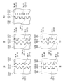
- FIG. 3 is a diagram illustrating a planar configuration example of an electrode in FIG. 2. It is a figure showing the other example of a cross-sectional structure of the light modulation element of FIG. It is a figure showing the example of a plane structure of the electrode of FIG. It is a figure which represents typically an example of an effect
- FIG. 12 is a diagram illustrating a perspective configuration example of the lens sheet in FIG. 11. It is a figure showing the 1st modification of the isometric view structure of the lens sheet of FIG. It is a figure showing the 2nd modification of the isometric view structure of the lens sheet of FIG.
- FIG. 12 It is a figure showing the 3rd modification of the isometric view structure of the lens sheet of FIG. It is a figure showing the cross-sectional structural example of the lens sheet of FIG. 12 with a light-guide plate and a light modulation element. It is a figure showing the 1st modification of the cross-sectional structure of the lens sheet of FIG. 12 with a light guide plate and a light modulation element. It is a figure showing the 2nd modification of the cross-sectional structure of the lens sheet of FIG. 12 with a light guide plate and a light modulation element. It is a figure showing the 3rd modification of the cross-sectional structure of the lens sheet of FIG. 12 with a light guide plate and a light modulation element.
- FIG. 12 shows the 3rd modification of the isometric view structure of the lens sheet of FIG.
- FIG. 15 is a diagram illustrating a cross-sectional configuration example of the lens sheet of FIG. 14 together with a light guide plate and a light modulation element. It is a figure showing the 1st modification of the cross-sectional structure of the lens sheet
- FIG. 24 is a diagram illustrating a first modification of the lens sheet of FIGS. 9, 10, and 12 to 23.
- FIG. 24 is a diagram illustrating a second modification of the lens sheet of FIGS. 9, 10, and 12 to 23. It is a figure showing a mode that the lens sheet
- FIG. 24 is a diagram illustrating a third modification of the lens sheet in FIGS. 9, 10, and 12 to 23.
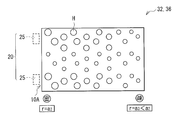
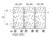
- FIG. 47 is a diagram illustrating an example of a pattern density distribution in the electrodes of FIGS. 43 to 46. It is a figure showing an example of luminance distribution when the electrode which has the pattern density of FIG. 47 is used.
- FIG. 47 is a schematic diagram for explaining an example of the operation of the light modulation element having the electrodes of FIGS. 43 to 46.
- FIG. 47 is a schematic diagram for explaining another example of the operation of the light modulation element having the electrodes of FIGS. 43 to 46.
- FIG. 47 is a schematic diagram for explaining another example of the operation of the light modulation element having the electrodes of FIGS. 43 to 46.
- It is a perspective view showing an example of composition of a light source of each embodiment.
- It is a perspective view showing an example of composition of a light guide plate of each embodiment.
- It is a schematic diagram showing an example of an effect
- FIG. It is a figure showing the 16th modification of the electrode of FIG. It is a figure showing the 17th modification of the electrode of FIG.
- FIG. 60 is a diagram illustrating an example of a pattern density distribution in the electrodes of FIGS. 43 to 46 and FIGS. 56 to 59.
- FIG. 61 is a diagram illustrating an example of a luminance distribution when an electrode having the pattern density of FIG. 60 is used. It is a figure showing the 20th modification of the electrode of FIG. It is a figure showing the 1st modification of the cross-sectional structure of the light modulation element of FIG. It is a figure showing the 2nd modification of the cross-sectional structure of the light modulation element of FIG.
- FIG. 68 is a diagram illustrating an example of functional blocks of a reception-side apparatus in FIG. 67.
- FIG. 68 is a diagram illustrating a cross-sectional configuration example of a display unit in the reception-side apparatus in FIG. 67.
- FIG. 68 is a diagram illustrating a cross-sectional configuration example of a display unit in the reception-side apparatus in FIG. 67.
- FIG. 68 is a perspective view illustrating an example of a relationship between a rubbing direction and a transmission axis of a polarizing plate in the reception-side apparatus in FIG. 67.
- FIG. 68 is a perspective view illustrating another example of the relationship between the rubbing direction and the transmission axis of the polarizing plate in the reception-side apparatus in FIG. 67.
- FIG. 69 is a schematic diagram for explaining a three-dimensional display in the display unit of FIG. 68.
- FIG. 69 is a schematic diagram for explaining a two-dimensional display in the display unit of FIG. 68.
- FIG. 68 is a cross-sectional view illustrating a first modification of the display unit in the reception-side apparatus in FIG. 67.
- FIG. 68 is a cross-sectional view illustrating a second modification of the display unit in the reception-side apparatus in FIG. 67.
- FIG. 76 is a diagram illustrating a cross-sectional configuration example of the parallax barrier of FIGS. 74 and 75. It is a schematic diagram showing an example of the relationship between the pixel of a display panel, and backlight light. It is a schematic diagram showing the other example of the relationship between the pixel of a display panel, and backlight light. It is a schematic diagram showing the other example of the relationship between the pixel of a display panel, and backlight light. It is a schematic diagram showing an example of the time division drive in a three-dimensional display. It is a schematic diagram showing an example of the time division drive following FIG.
- FIG. 83 is a schematic diagram illustrating an example of time-division driving following FIG. 82.
- FIG. 68 is a cross-sectional view illustrating a third modification of the display unit in the reception-side apparatus in FIG. 67.
- FIG. 68 is a cross-sectional view illustrating a fourth modification of the display unit in the reception-side apparatus in FIG. 67.
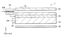
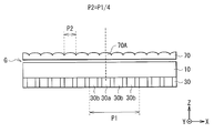
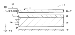
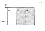
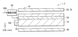
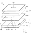
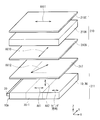
- FIG. 1 illustrates a cross-sectional configuration of the illumination device 1 according to the first embodiment of the present technology.
- the illumination device 1 can be applied as a backlight of a display device, and can output planar illumination light or a plurality of linear illumination lights as illumination light, as will be described in detail later.
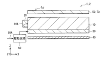
- the illuminating device 1 includes, for example, a light guide plate 10, a light source 20 disposed on a side surface of the light guide plate 10, a light modulation element 30 disposed inside the light guide plate 10, and a reflection plate 40 disposed behind the light guide plate 10.
- the lens sheet 50 disposed on the light guide plate 10 and a drive circuit 60 for driving the light modulation element 30 are provided.
- the light guide plate 10 corresponds to a specific example of “first transparent substrate” or “second transparent substrate” of the present technology.
- the light source 20 corresponds to a specific example of “light source” of the present technology.
- the optical system including the light source 20, the light modulation element 30, and the reflection plate 40 corresponds to a specific example of “illumination optical system” of the present technology.
- the lens sheet 50 corresponds to a specific example of “lens sheet” of the present technology.
- the light guide plate 10 guides light from the light source 20 disposed on the side surface of the light guide plate 10 to the upper surface side of the light guide plate 10 (specifically, the light exit surface 1A of the lighting device 1).
- the light guide plate 10 has a shape corresponding to an object to be irradiated (for example, a display panel 210 described later) disposed on the upper surface of the light guide plate 10. It has become.
- the side surface on which light from the light source 20 enters among the side surfaces of the light guide plate 10 is referred to as a light incident surface 10A.
- the light guide plate 10 has, for example, a predetermined patterned shape on at least one of an upper surface and a lower surface, and has a function of scattering and uniformizing light incident from the light incident surface 10A. Yes.
- a non-patterned flat light guide plate can be used as the light guide plate 10.
- the light guide plate 10 mainly includes a transparent thermoplastic resin such as polycarbonate resin (PC) or acrylic resin (polymethyl methacrylate (PMMA)).
- the light source 20 is a linear light source.
- a hot cathode fluorescent lamp (HCFL), a cold cathode fluorescent lamp (CCFL), or a plurality of LEDs (Light Emitting Diodes) are arranged in a line. It consists of things.
- the light source 20 is composed of a plurality of LEDs, it is preferable that all the LEDs are white LEDs from the viewpoints of efficiency, thickness reduction, and uniformity.
- the light source 20 may be configured to include, for example, a red LED, a green LED, and a blue LED.
- the light source 20 may be provided only on one side surface of the light guide plate 10 (see FIG. 1), or may be provided on two side surfaces, three side surfaces, or all side surfaces of the light guide plate 10.
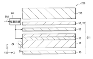
- the light modulation element 30 is in close contact with the inside of the light guide plate 10 without an air layer, and is adhered to the light guide plate 10 via, for example, an adhesive (not shown).
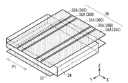
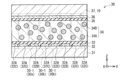
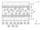
- the light modulation element 30 includes a transparent substrate 31, a lower electrode 32, an alignment film 33, a light modulation layer 34, an alignment film 35, an upper electrode 36, and a transparent substrate 37 on the reflection plate 40 side. Are arranged in order.
- FIG. 2 shows a cross-sectional configuration example of the light modulation element 30.
- the lower electrode 32 and the upper electrode 36 correspond to a specific example of “electrode” of the present technology.
- the light modulation layer 34 corresponds to a specific example of “light modulation layer” of the present technology.
- the transparent substrates 31 and 37 are arranged so as to be opposed to each other at a distance.
- the transparent substrates 31 and 37 support the light modulation layer 34 and are generally made of a substrate transparent to visible light, such as a glass plate or a plastic film.
- the upper electrode 36 and the lower electrode 32 generate an electric field for generating a plurality of linear scattering regions in the light modulation layer 34 in the three-dimensional display mode, and also in the two-dimensional display mode. An electric field for generating a planar scattering region is generated.
- the linear scattering area and the planar scattering area will be described in detail when the light modulation layer 34 is described.
- the upper electrode 36 is provided on the surface of the transparent substrate 37 facing the transparent substrate 31, and is composed of, for example, one sheet-like electrode (solid film) formed over the entire surface.
- the lower electrode 32 is provided on the surface of the transparent substrate 31 that faces the transparent substrate 37.
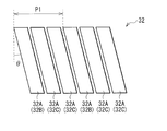
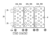
- the lower electrode 32 includes a plurality of partial electrodes 32A. ing.
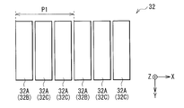
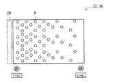
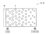
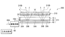
- FIG. 3 shows an example of a planar configuration of the lower electrode 32.
- the plurality of partial electrodes 32 ⁇ / b> A have a strip shape extending in one direction within the plane (for example, a direction parallel to the light incident surface 10 ⁇ / b> A). They are arranged side by side in a direction that intersects the extending direction of 32A.
- the arrangement direction of the plurality of partial electrodes 32A corresponds to the parallax direction in the three-dimensional display.
- a plurality of specific partial electrodes 32A hereinafter referred to as “partial electrodes 32B”) are used for generating linear illumination light when performing three-dimensional display in a display device. is there.
- the plurality of partial electrodes 32B are arranged at a pitch P1 (same pitch as the pixel pitch P2 or a pitch close thereto) corresponding to the pixel pitch P2 (see FIG. 72) when performing three-dimensional display in the display device.
- a plurality of partial electrodes 32A (hereinafter referred to as “partial electrodes 32C”) excluding the partial electrode 32B, together with the partial electrodes 32A, are used for planar illumination when performing two-dimensional display on the display device. It is used for light generation. That is, when performing two-dimensional display in the display device, all the partial electrodes 32A are used to generate planar illumination light.
- the plurality of partial electrodes 32B and the plurality of partial electrodes 32C are regularly arranged in a direction orthogonal to the light incident surface 10A. For example, as shown in FIGS.
- one partial electrode 32B and two partial electrodes 32C are used as a set, and a plurality of sets of partial electrodes are arranged in a direction orthogonal to the light incident surface 10A.
- the width of the partial electrode 32B is narrower than the width of the pixel of the display device.
- the partial electrode group does not always need to be composed of one partial electrode 32B and two partial electrodes 32C.
- the partial electrode group is composed of one partial electrode 32B and three partial electrodes 32C. May be.
- Each partial electrode 32A is, for example, not shown, but has a block shape, and a plurality of partial electrodes 32A may be two-dimensionally arranged.
- the plurality of partial electrodes 32A arranged in the Y-axis direction are regarded as one linear electrode, and the drive circuit 60 is configured so that each linear electrode functions as the partial electrodes 32B and 32C.
- the electrode 32A may be driven.
- a partial electrode 32 ⁇ / b> C having a width wider than the width of the partial electrode 32 ⁇ / b> B may be provided between the adjacent partial electrodes 32 ⁇ / b> B.
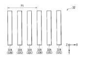
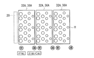
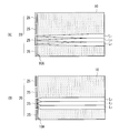
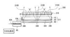
- FIG. 4 illustrates an example of a cross-sectional configuration of the light modulation element 30.
- FIG. 5 shows an example of a planar configuration of the lower electrode 32 of FIG.
- Both the lower electrode 32 and the upper electrode 36 are made of a transparent conductive film.
- This transparent conductive film is made of, for example, ITO.
- the lower electrode 32 and the upper electrode 36 may be made of indium zinc oxide (IZO), metal nanowires, carbon nanotubes, graphene, or the like.
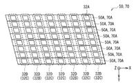
- a modulation cell 30-1 is configured (see FIG. 2).
- Each light modulation cell 30-1 corresponds to a specific example of the “linear scattering region” of the present technology, and a cell constituted by all the light modulation cells 30-1 is “plane-shaped” of the present technology. This corresponds to a specific example of “scattering region”.
- the light modulation cell 30-1 corresponds to a portion of the light modulation element 30 corresponding to a portion where the partial electrode 32A and the upper electrode 36 face each other.
- the light modulation cell 30a (see FIG. 2) including the partial electrode 32B among the plurality of light modulation cells 30-1 is used for generating linear illumination light when performing three-dimensional display in the display device.
- the light modulation cell 30b (see FIG. 2) including the partial electrode 32C among the plurality of light modulation cells 30-1 performs two-dimensional display on the display device, together with the plurality of light modulation cells 30a, the planar illumination light Used for generation. That is, when two-dimensional display is performed on the display device, all the light modulation cells 30-1 are used to generate planar illumination light.
- Each light modulation cell 30-1 can be driven independently by applying a predetermined voltage to the partial electrode 32A and the upper electrode 36.
- Each light modulation cell 30-1 exhibits transparency with respect to the light from the light source 20 or exhibits scattering depending on the magnitude of the voltage value applied to the partial electrode 32A and the upper electrode 36. It has become. The transparency and scattering properties will be described in detail when the light modulation layer 34 is described.
- the alignment films 33 and 35 are for aligning liquid crystals and monomers used for the light modulation layer 34, for example.
- the alignment film include a vertical alignment film and a horizontal alignment film.
- horizontal alignment films are used as the alignment films 33 and 35.
- the horizontal alignment film include an alignment film formed by rubbing polyimide, polyamideimide, polyvinyl alcohol, and the like, and an alignment film provided with a groove shape by transfer or etching.
- an alignment film formed by oblique deposition of an inorganic material such as silicon oxide, a diamond-like carbon alignment film formed by ion beam irradiation, an alignment formed with an electrode pattern slit A membrane is mentioned.
- the firing temperature after applying the alignment films 33 and 35 on the surfaces of the transparent substrates 31 and 37 in the manufacturing process is as low as possible.
- 35 is preferably a polyamideimide that can be formed at a temperature of 100 ° C. or lower.
- the alignment film When a voltage is used to form the alignment film, separate electrodes for alignment and driving may be formed, or a two-frequency liquid crystal in which the sign of dielectric anisotropy is inverted depending on the frequency may be used for the liquid crystal material. it can. Further, when a magnetic field is used for forming the alignment film, it is preferable to use a material having a large magnetic anisotropy as the alignment film, for example, a material having many benzene rings.
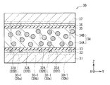
- the light modulation layer 34 is provided in the gap between the transparent substrate 31 and the transparent substrate 37.
- the light modulation layer 34 exhibits scattering or transparency with respect to the light from the light source 20 depending on the magnitude of the electric field.
- the light modulation layer 34 exhibits transparency with respect to light from the light source 20 when the electric field is relatively small, and exhibits scattering with respect to light from the light source 20 when the electric field is relatively large. It is.
- the light modulation layer 34 is a composite layer including a bulk 34A and a plurality of fine particles 34B dispersed in the bulk 34A.
- the bulk 34A and the fine particles 34B have optical anisotropy.
- FIG. 6A schematically shows an example of an orientation state in the fine particles 34B when no voltage is applied between the lower electrode 32 and the upper electrode 36.
- FIG. 6A the description of the orientation state in the bulk 34A is omitted.
- FIG. 6B shows an example of a refractive index ellipsoid showing the refractive index anisotropy of the bulk 34A and the fine particles 34B when no voltage is applied between the lower electrode 32 and the upper electrode 36.
- This refractive index ellipsoid is a tensor ellipsoid representing the refractive index of linearly polarized light incident from various directions.
- FIG. 6C shows an example of how the light L1 traveling in the front direction and the light L2 traveling in the oblique direction pass through the light modulation layer 34 when no voltage is applied between the lower electrode 32 and the upper electrode 36. This is a schematic representation.
- FIG. 7A schematically shows an example of an orientation state in the fine particles 34B when a voltage is applied between the lower electrode 32 and the upper electrode 36.
- FIG. 7A the description of the orientation state in the bulk 34A is omitted.
- FIG. 7B shows an example of a refractive index ellipsoid showing refractive index anisotropy of the bulk 34A and the fine particles 34B when a voltage is applied between the lower electrode 32 and the upper electrode 36.
- FIG. 7C shows an example of how light L1 traveling in the front direction and light L2 traveling in the oblique direction are scattered in the light modulation layer 34 when a voltage is applied between the lower electrode 32 and the upper electrode 36. Is a schematic representation.
- the bulk 34A and the fine particles 34B have an optical axis AX1 of the bulk 34A and an optical axis of the fine particles 34B when no voltage is applied between the lower electrode 32 and the upper electrode 36.
- the configuration is such that the directions of AX2 coincide with each other (become parallel).
- the optical axes AX1 and AX2 indicate lines parallel to the traveling direction of the light beam so that the refractive index becomes one value regardless of the polarization direction.
- the directions of the optical axis AX1 and the optical axis AX2 do not always have to coincide with each other, and the direction of the optical axis AX1 and the direction of the optical axis AX2 may be slightly shifted due to, for example, a manufacturing error.
- the fine particles 34B have a configuration in which the optical axis AX2 is parallel to the light incident surface 10A of the light guide plate 10 when no voltage is applied between the lower electrode 32 and the upper electrode 36, for example.
- the fine particles 34B further have a configuration in which, for example, the optical axis AX2 intersects the surfaces of the transparent substrates 31 and 37 at a slight angle ⁇ 1 when no voltage is applied between the lower electrode 32 and the upper electrode 36. (See FIG. 6B).
- the angle ⁇ 1 will be described in detail when the material constituting the fine particles 34B is described.
- the bulk 34A has a configuration in which, for example, the optical axis AX1 of the bulk 34A is constant regardless of whether or not voltage is applied between the lower electrode 32 and the upper electrode 36.
- the bulk 34A is a transparent substrate, for example, as shown in FIGS. 6A, 6B, 7A, and 7B, in which the optical axis AX1 of the bulk 34A is parallel to the light incident surface 10A of the light guide plate 10. It is configured to intersect the surfaces 31 and 37 at a predetermined angle ⁇ 1. That is, the optical axis AX1 of the bulk 34A is parallel to the optical axis AX2 of the fine particles 34B when no voltage is applied between the lower electrode 32 and the upper electrode 36.
- the optical axis AX2 is always parallel to the light incident surface 10A and does not need to intersect the surfaces of the transparent substrates 31 and 37 at an angle ⁇ 1, for example, due to manufacturing errors, It may intersect at an angle slightly different from the angle ⁇ 1.
- the optical axes AX1 and AX2 do not always have to be parallel to the light incident surface 10A, and may intersect the light incident surface 10A at a small angle due to, for example, manufacturing errors.
- the ordinary light refractive indexes of the bulk 34A and the fine particles 34B are equal to each other, and the extraordinary refractive indexes of the bulk 34A and the fine particles 34B are equal to each other.
- the light L1 traveling in the front direction and the light L2 traveling in the oblique direction pass through the light modulation layer 34 without being scattered in the light modulation layer 34.
- the light L from the light source 20 (light from the oblique direction) is an interface (transparent substrate) of the transparent region (transmission region 30 ⁇ / b> A) of the light modulation layer 34.
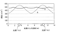
- 31 is totally reflected on the lower surface of 31 and the upper surface of the light guide plate 10, and the luminance of the transmission region 30 ⁇ / b> A (the luminance of black display) is lower than that in the case where the entire surface is uniformly illuminated (the dashed line in FIG. 8B).
- the front luminance profile of FIG. 8B is obtained by installing a diffusion sheet (not shown) on the light guide plate 10 and measuring through the diffusion sheet.
- a low refractive index material is typically air.
- the low refractive index material in contact with the upper surface of the light guide plate 10 is an adhesive or an adhesive. May be.
- the directions of the optical axis AX1 and the optical axis AX2 are different from each other as shown in FIGS. 7A and 7B. It has a configuration (intersecting or almost orthogonal).
- the fine particle 34B has the optical axis AX2 of the fine particle 34B parallel to the light incident surface 10A of the light guide plate 10 and the transparent substrate 31, It intersects with the surface of 37 at an angle ⁇ 2 (for example, 90 °) larger than the angle ⁇ 1.
- the angle ⁇ 2 will be described in detail when the material constituting the fine particles 34B is described.
- the refractive index difference increases in all directions including the front direction and the oblique direction in the light modulation layer 34, and a high scattering property is obtained.
- the light L1 traveling in the front direction and the light L2 traveling in the oblique direction are scattered in the light modulation layer 34.
- the light L from the light source 20 passes through the interface of the scattering region 30B (the interface between the transparent substrate 31 or the light guide plate 10 and air).
- the light transmitted to the reflecting plate 40 side is reflected by the reflecting plate 40 and passes through the light modulation element 30. Therefore, the brightness of the scattering region 30B is extremely higher than that when the entire surface is made to emit light uniformly (the one-dot chain line in FIG. 8B), and a partial white display corresponding to the reduction in the brightness of the transmission region 30A. The brightness (increased brightness) increases.
- the ordinary light refractive indexes of the bulk 34A and the fine particles 34B may be slightly deviated due to, for example, a manufacturing error, for example, preferably 0.1 or less, and more preferably 0.05 or less. Further, the extraordinary refractive indexes of the bulk 34A and the fine particles 34B may be slightly deviated due to, for example, manufacturing errors, and are preferably 0.1 or less, more preferably 0.05 or less.
- the bulk 34A and the fine particles 34B have different response speeds with respect to the electric field.
- the bulk 34A has, for example, a streak structure, a porous structure, or a rod-like structure having a response speed slower than that of the fine particles 34B.
- the bulk 34A is formed of, for example, a polymer material obtained by polymerizing a low molecular weight monomer.
- the bulk 34A is obtained by polymerizing a material having alignment properties and polymerizability (for example, a monomer) aligned along the alignment direction of the fine particles 34B or the alignment directions of the alignment films 33 and 35 with at least one of heat and light. Is formed.
- the streaky structure, the porous structure, or the rod-shaped structure of the bulk 34A is, for example, parallel to the light incident surface 10A of the light guide plate 10 and has a long axis in a direction intersecting the surfaces of the transparent substrates 31 and 37 at a slight angle ⁇ 1.
- the average streak size in the short axis direction is 0.1 ⁇ m or more and 10 ⁇ m or less from the viewpoint of increasing the light scattering property. It is preferable that the thickness is in the range of 0.2 ⁇ m to 2.0 ⁇ m.
- the scattering ability in the light modulation element 30 is substantially equal in the visible region of 380 to 780 nm. For this reason, only light of a specific wavelength component does not increase or decrease in the plane, so that a balance in the visible region can be achieved in the plane.
- the average streak size in the minor axis direction is less than 0.1 ⁇ m or more than 10 ⁇ m, the light modulation element 30 has low scattering ability regardless of the wavelength, and the light modulation element 30 is light modulated. It is difficult to function as an element.
- the average streak size in the minor axis direction is preferably in the range of 0.5 ⁇ m to 5 ⁇ m, and preferably in the range of 1 to 3 ⁇ m. Is more preferable.
- the wavelength dependence of scattering in the bulk 34A. Sex is suppressed.
- the size of the streak tissue can be observed with a polarizing microscope, a confocal microscope, an electron microscope, or the like.
- the fine particles 34B are mainly composed of, for example, a liquid crystal material, and have a response speed sufficiently faster than the response speed of the bulk 34A.
- the liquid crystal material (liquid crystal molecules) contained in the fine particles 34B is, for example, a rod-like molecule.
- the liquid crystal molecules contained in the fine particles 34B those having positive dielectric anisotropy (so-called positive liquid crystal) are preferably used.
- the major axis direction of the liquid crystal molecules is parallel to the optical axis AX1 in the fine particles 34B.
- the major axis of the liquid crystal molecules in the fine particles 34B is parallel to the light incident surface 10A of the light guide plate 10 and intersects the surfaces of the transparent substrates 31 and 37 at a slight angle ⁇ 1. That is, the liquid crystal molecules in the fine particles 34B are aligned in a state inclined by an angle ⁇ 1 in a plane parallel to the light incident surface 10A of the light guide plate 10 when no voltage is applied between the lower electrode 32 and the upper electrode 36. is doing.
- This angle ⁇ 1 is called a pretilt angle, and is preferably in the range of 0.1 ° to 30 °, for example.
- the angle ⁇ 1 is more preferably in the range of 0.5 ° to 10 °, and still more preferably in the range of 0.7 ° to 2 °.
- Increasing the angle ⁇ 1 tends to decrease the scattering efficiency for reasons described later.
- the angle ⁇ 1 is too small, the azimuth angle at which the liquid crystal rises varies when a voltage is applied. For example, the liquid crystal may rise in a direction opposite to 180 ° (reverse tilt). Thereby, since the refractive index difference between the fine particles 34B and the bulk 34A cannot be used effectively, the scattering efficiency tends to be low and the luminance tends to be low.
- the major axis direction of the liquid crystal molecules intersects (or is orthogonal to) the optical axis AX1 in the fine particles 34B.
- the major axis of the liquid crystal molecules in the fine particles 34B is parallel to the light incident surface 10A of the light guide plate 10 and intersects the surfaces of the transparent substrates 31 and 37 at an angle ⁇ 2 (for example, 90 °) larger than the angle ⁇ 1. ing.
- any material that has optical anisotropy and is combined with liquid crystal may be used, but in this embodiment, a low molecular weight monomer that cures with ultraviolet rays. It is preferable that It is preferable that the direction of optical anisotropy between the liquid crystal and the one formed by polymerizing a low molecular weight monomer (polymer material) in the state where no voltage is applied is the same before UV curing.
- the liquid crystal and the low molecular weight monomer are preferably aligned in the same direction.
- the shape of the monomer material used is preferably rod-shaped.
- a material having both polymerizability and liquid crystallinity as the monomer material. It preferably has at least one functional group selected from the group consisting of These functional groups can be polymerized by irradiation with ultraviolet rays, infrared rays or electron beams, or by heating. A liquid crystalline material having a polyfunctional group can also be added in order to suppress a decrease in the degree of alignment during ultraviolet irradiation.
- a bifunctional liquid crystalline monomer as a raw material for the bulk 34A.
- a monofunctional monomer can be added to the raw material of the bulk 34A for the purpose of adjusting the temperature showing liquid crystallinity, or a trifunctional or higher functional monomer can be added for the purpose of improving the crosslinking density.
- the reflection plate 40 returns light leaking from the back of the light guide plate 10 through the light modulation element 30 to the light guide plate 10 side.
- the reflector 40 has functions such as reflection, diffusion, and scattering. Thereby, the emitted light from the light source 20 can be used efficiently, and it is also useful for improving the front luminance.
- the reflection plate 40 is made of, for example, foamed PET (polyethylene terephthalate), a silver vapor deposition film, a multilayer film reflection film, or white PET.
- the reflecting plate 40 has a function of regular reflection (specular reflection)
- the reflecting plate 40 is preferably composed of, for example, a silver vapor deposition film, a multilayer film reflection film, an aluminum vapor deposition film, or the like. Further, the reflector 40 may be provided with a shape for reflecting light in a specific direction.
- the lens sheet 50 narrows the divergence angle of light (illumination light) emitted from the upper surface of the light guide plate 10. For example, as shown in FIG. 1, the lens sheet 50 is guided so that a gap is formed between the light incident surface (lower surface) of the lens sheet 50 and the light emitting surface (upper surface) of the light guide plate 10. It is disposed on the light plate 10.
- the gap is a layer filled with a material having a refractive index lower than the refractive index of the light emitting surface (upper surface) of the light guide plate 10, and is, for example, an air layer.
- the gap does not always need to be an air layer, for example, a layer filled with a pressure-sensitive adhesive or adhesive made of a material having a refractive index lower than the refractive index of the light exit surface (upper surface) of the light guide plate 10. It may be.
- the gap is filled with a material having a refractive index close to that of the light guide plate 10. It may be a layer. In this case, the lens sheet 50 is adhered or adhered to the light emitting surface (upper surface) of the light guide plate 10 with an adhesive or an adhesive.
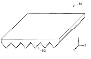
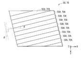
- the lens sheet 50 has a concavo-convex surface in which a plurality of belt-like convex portions 50 ⁇ / b> A are arranged in a direction intersecting with the extending direction of the belt-like convex portions 50 ⁇ / b> A.
- the uneven surface may be arranged on the light emitting side of the lens sheet 50, but as shown in FIG. 10, the light incident side (light modulation layer 34) of the lens sheet 50. Side). In the case where the uneven surface is disposed on the light incident side of the lens sheet 50, light at a shallow angle among the light emitted from the light guide plate 10 can be raised vertically.
- the cross section of the belt-like convex portion 50A is preferably a triangular shape with a base angle of 60 ° to 70 °, and more preferably a triangular shape with a base angle of 60 ° to 65 °.
- the ridge line direction of the belt-like convex portion 50A is preferably parallel to the arrangement of the lower electrode 32 (or the light modulation cell 30a).
- the surface opposite to the concavo-convex surface is, for example, a flat surface as shown in FIGS. In this case, the flat surface of the lens sheet 50 can be directly bonded to the display panel using an adhesive or an adhesive.
- the belt-like convex portion 50A is formed of a UV curable resin or the like, it can be directly formed on the display panel.
- the lens sheet 50 is disposed such that the flat surface is parallel or substantially parallel to the upper surface of the light guide plate 10.
- the band-shaped convex portion 50A extends in a direction parallel to the extending direction of the lower electrode 32 (or the light modulation cell 30a).
- the light modulation cell 30a is in the scattering state, the light modulation cell 30a is a linear scattering region. Therefore, at this time, it can be said that the belt-like convex portion 50A extends in a direction parallel to the extending direction of the linear scattering region.
- the cross section of the belt-like convex portion 50A (the cross section in the width direction of the belt-like convex portion 50A) has, for example, a triangular shape as shown in FIGS.
- the cross-sectional shape of the belt-like convex portion 50A does not always need to be a triangular shape, and may be a polygonal shape.
- the belt-like convex portion 50 ⁇ / b> A has a convex shape that protrudes to the side opposite to the flat surface side of the lens sheet 50.
- the pitch of the uneven surface of the lens sheet 50 is preferably as small as possible from the viewpoint of minimizing the decrease in contrast.
- the pitch of an uneven surface is equal to the pitch of 50 A of strip
- the pitch of the uneven surface is equal to the period of periodic change of the width of the belt-like convex portion 50A.
- the lens sheet 50 is preferably made of a material having an isotropic refractive index.
- Light emitted from the upper surface of the light guide plate 10 is polarized light. Therefore, for example, when it is preferable from the viewpoint of improving the brightness of the display panel that the light emitted from the illumination device 1 is polarized light, the light emitted from the upper surface of the light guide plate 10 is used as it is. What is necessary is just to utilize as 1 emitted light. However, when the lens sheet 50 has a large phase difference, the polarization component of the light emitted from the illumination device 1 is disturbed by the lens sheet 50. Therefore, from the viewpoint of not disturbing the polarization component of the light emitted from the upper surface of the light guide plate 10, the lens sheet 50 is preferably made of a material having an isotropic refractive index.
- the optical axis AX2 of the fine particle 34B in one light modulation cell 30-1 is parallel or substantially parallel to the optical axis AX1 of the bulk 34A, and the optical axis of the fine particle 34B in the other light modulation cell 30-1.
- the magnitude of the voltage applied to the pair of electrodes (partial electrode 32A, upper electrode 36) of each light modulation cell 30-1 is controlled so that AX2 intersects or is orthogonal to the optical axis AX1 of the bulk 34A. . That is, the drive circuit 60 can make the directions of the optical axes AX1 and AX2 of the bulk 34A and the fine particles 34B coincide (or substantially coincide) with each other or can be different (or orthogonal) by electric field control. It has become.
- the drive circuit 60 outputs a plurality of linear illumination lights from the light modulation element 30 when a signal designating three-dimensional display is input as the control signal 60A (that is, in the three-dimensional display mode). ing. Specifically, the drive circuit 60 applies a voltage at which the light modulation layer 34 exhibits scattering properties to a specific plurality of partial electrodes 32B among the plurality of partial electrodes 32A, and a plurality of the plurality of partial electrodes 32A. The light modulation layer 34 applies a voltage indicating transparency to the plurality of partial electrodes 32C excluding the partial electrode 32B.
- the optical axis AX2 of the fine particle 34B intersects the optical axis AX1 of the bulk 34A in each light modulation cell 30a in the light modulation element 30, and the fine particle 34B in the light modulation cell 30b in the light modulation element 30.
- the magnitude of the voltage applied to the pair of electrodes (partial electrode 32A, upper electrode 36) of each light modulation cell 30-1 is controlled so that the optical axis AX2 of the light is parallel to the optical axis AX1 of the bulk 34A. It has become.
- the drive circuit 60 causes the light modulation cell 30a including the partial electrode 32B to generate the linear scattering region 30B, and causes the light modulation cell 30b including the partial electrode 32C to generate the linear transmission region 30A. Thereby, linear illumination light is output from the scattering region 30B.
- the drive circuit 60 when a signal designating two-dimensional display is input as the control signal 60A (that is, in the two-dimensional display mode), the drive circuit 60 outputs planar illumination light from the light modulation element 30. ing. Specifically, the drive circuit 60 applies a voltage at which the light modulation layer 34 exhibits scattering properties to each partial electrode 32A. In other words, the drive circuit 60 is configured so that the optical axis AX2 of the fine particles 34B intersects or is orthogonal (or substantially orthogonal) to the optical axis AX1 of the bulk 34A in all the light modulation cells 30-1 included in the light modulation element 30. The magnitude of the voltage applied to the pair of electrodes (partial electrode 32A, upper electrode 36) of each light modulation cell 30-1 is controlled. As a result, the drive circuit 60 causes each light modulation cell 30-1 to generate the scattering region 30B, thereby causing the planar illumination light to be output from the planar scattering region 30B.
- the optical axis AX2 of the fine particle 34B intersects or is orthogonal to the optical axis AX1 of the bulk 34A in each light modulation cell 30a, and the fine particle 34B in each light modulation cell 30b.
- a voltage is applied to the pair of electrodes (partial electrode 32A, upper electrode 36) of each light modulation cell 30-1 so that the optical axis AX2 of the light is parallel or substantially parallel to the optical axis AX1 of the bulk 34A.
- the light emitted from the light source 20 and entering the light guide plate 10 is transmitted through the transmission region 30A of the light modulation element 30, and is scattered in the scattering region 30B of the light modulation element 30 (FIG. 8).
- the light transmitted through the lower surface of the scattering region 30 ⁇ / b> B is reflected by the reflecting plate 40, returned again to the light guide plate 10, and then emitted from the upper surface of the lighting device 1.
- light scattered toward the upper surface of the scattering region 30 ⁇ / b> B is emitted from the upper surface of the illumination device 1 after passing through the light guide plate 10.
- the optical axis AX2 of the fine particle 34B intersects or is orthogonal to the optical axis AX1 of the bulk 34A.
- a voltage is applied to a pair of electrodes (partial electrode 32A, upper electrode 36) of each light modulation cell 30-1.
- the light transmitted through the lower surface of the scattering region 30 ⁇ / b> B is reflected by the reflecting plate 40, returned again to the light guide plate 10, and then emitted from the upper surface of the lighting device 1.
- light scattered toward the upper surface of the scattering region 30 ⁇ / b> B is emitted from the upper surface of the illumination device 1 after passing through the light guide plate 10.
- a lens sheet 50 that narrows the divergence angle of illumination light is provided.
- luminance of a front direction can be made high compared with the case where the lens sheet 50 is not provided.
- the amount of light incident on the display panel in the display device at an angle of 0 ° to an appropriate viewing angle (for example, 15 °) can be increased. Therefore, high luminance can be obtained in the display image.
- PDLC is formed by mixing liquid crystal material and isotropic low molecular weight material and causing phase separation by ultraviolet irradiation or solvent drying, and the fine particles of liquid crystal material are dispersed in the polymer material. It is a composite layer.
- the liquid crystal material in this composite layer has a scattering property because it is oriented in a random direction when no voltage is applied, but is oriented in the electric field direction when a voltage is applied. Are equal to each other, high transparency is exhibited in the front direction (normal direction of PDLC).
- the difference between the extraordinary refractive index of the liquid crystal material and the refractive index of the polymer material becomes significant in the oblique direction, and even if the front direction is transparent, the scattering property is exhibited in the oblique direction. End up.
- a light modulation element using PDLC often has a structure in which PDLC is sandwiched between two glass plates having a transparent conductive film formed on the surface thereof.
- the light incident from the oblique direction is refracted due to the difference in refractive index between the air and the glass plate, and at a smaller angle.
- the light enters the PDLC. Therefore, no large scattering occurs in such a light modulation element. For example, when light is incident at an angle of 80 degrees from the air, the incident angle of the light on the PDLC is reduced to about 40 degrees due to refraction at the glass interface.
- the front direction (the normal direction of the PDLC)
- the difference in refractive index increases in the oblique direction.
- an optical film such as a diffusion film
- oblique leakage light is also diffused in the front direction by the diffusion film, etc., so that light leakage in the front direction increases, and the modulation ratio in the front direction is increased. Will be lower.
- the bulk 34A and the fine particles 34B are mainly formed of the optically anisotropic material, the scattering property is reduced in the oblique direction, and the transparency can be improved.
- the bulk 34 ⁇ / b> A and the fine particles 34 ⁇ / b> B mainly include optically anisotropic materials having the same ordinary light refractive index and the same extraordinary light refractive index, and a voltage between the lower electrode 32 and the upper electrode 36. In the region where no is applied, the directions of these optical axes coincide or almost coincide. Thereby, the refractive index difference is reduced or eliminated in all directions including the front direction (normal direction of the light modulation element 30) and the oblique direction, and high transparency is obtained. As a result, light leakage in a wide viewing angle range can be reduced or almost eliminated, and viewing angle characteristics can be improved.
- a liquid crystal having an ordinary light refractive index of 1.5 and an extraordinary light refractive index of 1.65 is mixed with a liquid crystalline monomer having an ordinary light refractive index of 1.5 and an extraordinary light refractive index of 1.65, and the liquid crystal is formed by an alignment film or an electric field.
- the liquid crystalline monomer is polymerized with the liquid crystalline monomer aligned, the optical axis of the liquid crystal and the optical axis of the polymer formed by the polymerization of the liquid crystalline monomer coincide with each other.
- the refractive index can be made to coincide in all directions, in such a case, a highly transparent state can be realized, and the viewing angle characteristics can be further improved.
- the luminance of the transmissive region 30A (black display luminance) is uniformly emitted over the entire surface (the chain line in FIG. 8B). It is lower than On the other hand, the brightness of the scattering region 30B is extremely higher than that when the entire surface is made to emit light uniformly (the one-dot chain line in FIG. 8B), and a partial white display corresponding to the reduction in the brightness of the transmission region 30A. The brightness (increased brightness) increases.
- increasing the brightness is a technique for increasing the brightness when a partial white display is performed as compared with the case where the entire white display is performed.
- This technique is commonly used in CRT and PDP.
- the backlight emits light uniformly regardless of the image, so the brightness cannot be partially increased.
- the backlight is an LED backlight in which a plurality of LEDs are two-dimensionally arranged, the LEDs can be partially turned off.
- the luminance is lower than when all the LEDs are turned on.
- it is possible to increase the brightness by increasing the current flowing to the partially lit LED, but in such a case, a large current flows in a very short time, Problems remain in terms of circuit load and reliability.
- the bulk 34A and the fine particles 34B are mainly formed by including an optically anisotropic material, scattering in an oblique direction is suppressed, and light leaked from the light guide plate in a dark state is prevented. Few. Thereby, since the light is guided from the partial dark state portion to the partial bright state portion, it is possible to increase the luminance without increasing the input power to the lighting device 1.
- the optical axis AX2 of the fine particles 34B is parallel to the light incident surface 10A of the light guide plate 10, In addition, it intersects the surfaces of the transparent substrates 31 and 37 at a slight angle ⁇ 1. That is, the liquid crystal molecules contained in the fine particles 34B are aligned in a state inclined by an angle ⁇ 1 (a state where a pretilt angle is given) in a plane parallel to the light incident surface 10A. Therefore, when a voltage is applied between the lower electrode 32 and the upper electrode 36, the liquid crystal material contained in the fine particles 34B does not rise in a random orientation but rises in a plane parallel to the light incident surface 10A.
- the optical axes AX1 and AX2 of the bulk 34A and the fine particles 34B intersect or are orthogonal to each other in a plane parallel to the light incident surface 10A.
- the light that vibrates perpendicularly to the transparent substrate 31 feels the difference between the extraordinary refractive index of the fine particles 34B and the ordinary refractive index of the bulk 34A.
- the difference between the extraordinary refractive index of the fine particles 34 ⁇ / b> B and the ordinary refractive index of the bulk 34 ⁇ / b> A is large, the scattering efficiency of light oscillating perpendicularly to the transparent substrate 31 is increased.
- the light oscillating parallel to the transparent substrate 31 feels the difference between the ordinary light refractive index of the fine particles 34B and the extraordinary light refractive index of the bulk 34A.
- the difference between the ordinary light refractive index of the fine particles 34B and the extraordinary light refractive index of the bulk 34A is large, the scattering efficiency of light oscillating parallel to the transparent substrate 31 is also increased. Therefore, the light propagating through the region where the voltage is applied between the lower electrode 32 and the upper electrode 36 includes a large amount of oblique components.
- an acrylic light guide plate is used as the light guide plate 10
- light in a region where a voltage is applied between the lower electrode 32 and the upper electrode 36 propagates at an angle of 41.8 degrees or more.
- the refractive index difference is increased in all directions including the oblique direction, and high scattering properties can be obtained, so that the display luminance can be improved.
- the display brightness can be further improved by the effect of increasing the brightness.
- the optical axes AX1 and AX2 of the bulk 34A and the fine particles 34B are arranged perpendicular to the light incident surface 10A of the light guide plate 10, and a voltage is applied between the lower electrode 32 and the upper electrode 36.
- the liquid crystal material contained in the fine particles 34B rises in a plane perpendicular to the light incident surface 10A, the light oscillating perpendicularly to the transparent substrate 31 is the same as described above.
- the difference between the extraordinary refractive index of the fine particles 34B and the ordinary refractive index of the bulk 34A is the difference between the ordinary refractive index of the fine particles 34B and the ordinary refractive index of the bulk 34A. You will feel the difference.
- the scattering efficiency of light oscillating perpendicularly to the transparent substrate 31 is high, but the scattering efficiency of light oscillating parallel to the transparent substrate 31 is low or zero. Therefore, when the optical axes AX1 and AX2 are arranged perpendicular to the light incident surface 10A, the scattering efficiency is lower than when the optical axes AX1 and AX2 are arranged parallel to the light incident surface 10A. Therefore, the luminance that can be extracted from the light guide plate 10 is lower than that of the light modulation element 30 of the present embodiment.
- display luminance can be improved while reducing or hardly eliminating light leakage in a range with a large viewing angle.
- the modulation ratio in the front direction can be increased.
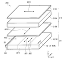
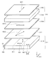
- FIG. 11 illustrates a cross-sectional configuration of the illumination device 2 according to the second embodiment of the present technology.
- the illumination device 2 can be applied as a backlight of a display device, and can output planar illumination light or a plurality of linear illumination lights as illumination light, similar to the illumination device 1 according to the embodiment. It is.
- the illumination device 2 includes, for example, a light guide plate 10, a light source 20, a light modulation element 30, a reflection plate 40, a drive circuit 60, and a lens sheet 70.
- the lens sheet 70 is disposed on the light guide plate 10. That is, the illumination device 2 corresponds to the illumination device 1 according to the first embodiment provided with the lens sheet 70 instead of the lens sheet 50.
- the lens sheet 70 corresponds to a specific example of “lens sheet” of the present technology.
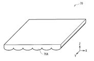
- FIG. 12 shows a perspective configuration example of the lens sheet 70.
- the lens sheet 70 narrows the divergence angle of light (illumination light) emitted from the upper surface of the light guide plate 10.
- the lens sheet 70 is guided so that a gap is formed between the light incident surface (lower surface) of the lens sheet 70 and the light emitting surface (upper surface) of the light guide plate 10. It is disposed on the light plate 10.
- the gap is a layer filled with a material having a refractive index lower than the refractive index of the light emitting surface (upper surface) of the light guide plate 10 as in the above embodiment, for example, an air layer.
- the gap does not always need to be an air layer, for example, a layer filled with a pressure-sensitive adhesive or adhesive made of a material having a refractive index lower than the refractive index of the light exit surface (upper surface) of the light guide plate 10. It may be.
- a pressure-sensitive adhesive or adhesive made of a material having a refractive index lower than the refractive index of the light exit surface (upper surface) of the light guide plate 10. It may be.
- the gap is filled with a material having a refractive index close to that of the light guide plate 10. It may be a layer.
- the lens sheet 70 is adhered or adhered to the light emitting surface (upper surface) of the light guide plate 10 with an adhesive or an adhesive.
- the lens sheet 70 has a concavo-convex surface in which a plurality of belt-like convex portions 70 ⁇ / b> A are arranged in a direction intersecting with the extending direction of the belt-like convex portions 70 ⁇ / b> A.
- the uneven surface may be arranged on the light emitting side of the lens sheet 70, or arranged on the light incident side of the lens sheet 70 as shown in FIG. 13. Also good. However, when the uneven surface is arranged on the light incident side of the lens sheet 70, the uneven surface can be brought closer to the upper surface of the light guide plate 10.
- the design freedom of the thickness of the light-guide plate 10 and the transparent substrate 37 can be made high by the thickness of the base material which comprises the lens sheet 70.
- FIG. in the lens sheet 70 the surface opposite to the uneven surface is, for example, a flat surface as shown in FIGS.
- the flat surface of the lens sheet 70 can be directly bonded to the display panel using an adhesive or an adhesive.
- the belt-like convex portion 70A is formed of a UV curable resin or the like, the belt-like convex portion 70A can be directly formed on the display panel.
- the lens sheet 70 is disposed such that the flat surface is parallel or substantially parallel to the upper surface of the light guide plate 10.
- the strip-shaped convex portion 70A extends in a direction parallel to the extending direction of the lower electrode 32 (or the light modulation cell 30a).
- the light modulation cell 30a is in the scattering state, the light modulation cell 30a is a linear scattering region. Therefore, at this time, it can be said that the belt-like convex portion 70A extends in a direction parallel to the extending direction of the linear scattering region.
- the cross section of the belt-like convex portion 70A (the cross section in the width direction of the belt-like convex portion 70A) has, for example, a cylindrical shape as shown in FIGS.
- the cylindrical shape is a shape that can increase the front luminance while minimizing the decrease in contrast because the reflection as in the case of the triangular shape is not used.
- Examples of the cylindrical shape include a circular shape as shown in FIGS. 12 and 13 and an aspherical shape as shown in FIGS. 14 and 15.
- the focal length of the belt-like convex portion 70A can be increased.
- the distance between the light modulation cell 30a and the belt-like convex portion 70A can be increased by the length of the focal length of the belt-like convex portion 70A, so that the thickness of the light guide plate 10 and the transparent substrate 37 can be freely designed. The degree can be increased.
- the belt-like convex portion 70 ⁇ / b> A has a convex shape protruding to the side opposite to the flat surface side of the lens sheet 70.
- 14 is a perspective configuration example when the belt-like convex portion 70A is disposed on the light emitting side of the lens sheet 70
- FIG. 15 is a perspective view of the belt-like convex portion 70A disposed on the light incident side of the lens sheet 70.
- the shape of the end corresponds to the shape when -1 ⁇ k ⁇ 0 in the following conic surface.
- the shape of the end corresponds to the shape when k ⁇ 1 on the conic surface shown below.
- ⁇ 40 ⁇ k ⁇ 0 More preferably, -30 ⁇ k ⁇ -4.
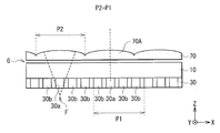
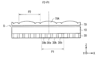
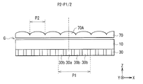
- FIG. 16 to 23 show an example of a cross-sectional configuration of the lens sheet 70 together with the light guide plate 10 and the light modulation element 30.
- FIG. 16 to 19 illustrate the belt-like convex portion 70A having a circular cross section.
- FIGS. 20 to 23 exemplify the belt-like convex portion 70A having an aspherical cross section.
- the pitch P2 of the uneven surface is, for example, P1, as shown in FIGS.
- the widths of the belt-like convex portions 70A do not always have to be equal to each other.
- FIGS. May be arranged.
- the pitch P2 of the uneven surface is, for example, FIG. As shown in FIG. 22, it may be P1 / 2 or, for example, it may be P1 / 4 as shown in FIGS.
- the radius R of the belt-like convex portion 70A is P1 / N ⁇ 0.6 ⁇ R ⁇ P1 / where P1 is the pitch of the light modulation cell 30a (part that can be a linear scattering region) and N is the number of three-dimensional viewpoints. N ⁇ 1.4 is preferred. Furthermore, it is more preferable that P1 / N ⁇ 0.8 ⁇ R ⁇ P1 / N ⁇ 1.2.
- the belt-like convex portion 70A is arranged so that the center in the width direction of the belt-like convex portion 70A faces the light modulation cell 30a (part that can be a linear scattering region).
- belt-shaped convex parts are preferably arrange
- the distance Lz between the belt-like convex portion 70A and the light modulation cell 30a is set such that the radius of curvature of the belt-like convex portion 70A is R, the refractive index of the belt-like convex portion 70A is n1, and the distance between the belt-like convex portion 70A and the light modulation cell 30a.
- Is preferably 0 ⁇ Lz ⁇ R / (n2 (n1-1)) ⁇ 1.4.
- the brightness in the front direction is higher than that in the case where the distance Lz between the belt-shaped convex portion 70A and the light modulation cell 30a is located at a position farther from the above range.
- the lens sheet 70 is preferably made of a material having an isotropic refractive index.
- the light emitted from the upper surface of the light guide plate 10 is polarized light having a polarization axis in a direction parallel to the optical axis AX1 of the bulk 34A having low electric field response. Therefore, for example, when it is preferable from the viewpoint of improving the brightness of the display panel that the light emitted from the illumination device 2 is polarized light, the light emitted from the upper surface of the light guide plate 10 is disturbed in polarization. What is necessary is just to utilize as emitted light of the illuminating device 2 as it is.
- the lens sheet 70 has a large phase difference, the polarization component of the light emitted from the illumination device 2 is disturbed by the lens sheet 70. Therefore, from the viewpoint of not disturbing the polarization component of the light emitted from the upper surface of the light guide plate 10, the lens sheet 70 is preferably made of a material having an isotropic refractive index.
- the lens sheet 70 which narrows the divergence angle of illumination light is provided.
- luminance of a front direction can be made high compared with the case where the lens sheet 70 is not provided.
- the amount of light incident on the display panel in the display device at an angle of 0 ° to an appropriate viewing angle can be increased. Therefore, high luminance can be obtained in the display image.
- each partial electrode 32A extends in a direction parallel to the light incident surface 10A.
- You may extend in the direction which crosses diagonally.
- the extending direction of each partial electrode 32 ⁇ / b> A extends in a direction intersecting with an arrangement direction of pixels of a display panel 210 (described later with reference to FIG. 70).
- the difference between the resolution in the direction parallel to the normal line of the light incident surface 10A and the resolution in the direction parallel to the light incident surface 10A can be reduced.
- the width of the partial electrode 32A may be narrow.
- the emission line width (the width of the scattering region) in the illumination devices 1 and 2 is reduced.
- the illumination devices 1 and 2 are used as the backlight of the display device, it is possible to make it difficult to see the double image formed in the front direction of the display device during three-dimensional display.
- the width of the partial electrode 32A is narrow, the light collection rate by the lens is increased, and the front luminance can be increased.
- the illumination devices 1 and 2 are used as illumination light by planar illumination light, a plurality of linear illumination lights, or a plurality of dotted illumination lights arranged in a line. It may be capable of outputting the formed linear illumination light.
- each partial electrode 32A may have a block shape, and a plurality of partial electrodes 32A may be two-dimensionally arranged. In this case, when the plurality of partial electrodes 32A arranged in a row are regarded as one linear electrode 32D, each linear electrode 32D may be used as the partial electrodes 32B and 32C.
- a specific plurality of linear electrodes 32D among the plurality of linear electrodes 32D are used as the partial electrodes 32B.
- a plurality of linear electrodes 32D excluding those used as the partial electrode 32B among the plurality of linear electrodes 32D are used as the partial electrode 32C. That is, in the present modification, when the lower electrode 32 is in the three-dimensional display mode, a plurality of dotted scattering regions (substantially linear scattering regions) arranged in a line with respect to the light modulation layer 34 are displayed. The electric field to be generated is generated in multiple rows.
- the illumination devices 1 and 2 according to the present modification are formed by “a plurality of dotted scattering regions arranged in a line” in the “line scattering region” in the description of each of the embodiments and the modifications 1 and 2.
- the configuration is equivalent to that read as “linear scattering region”.
- the partial electrodes 32A included in the linear electrode 32D may be formed separately from each other, or may be connected to each other via a thin line (not shown).
- the linear electrode 32D is a so-called stepped electrode.
- the illuminating devices 1 and 2 emit linear illumination light or a plurality of dot illumination lights (substantially linear illumination light) arranged in a row corresponding to each linear electrode 32D. It is supposed to be.
- each linear electrode 32D extends in a direction obliquely intersecting the light incident surface 10A, for example, as shown in FIG. You may extend in the direction which cross
- the belt-like convex portions 50A and 70A preferably extend in a direction parallel to the extending direction of each linear electrode 32D. At this time, the belt-like convex portions 50A and 70A are parallel to the extending direction of the scattering region (a plurality of dotted scattering regions (substantially linear scattering regions) arranged in a row) generated corresponding to the linear electrode 32D. It is preferable to extend in any direction.
- the partial electrode 32A is not opposed to the two belt-like convex portions 50A (or the two belt-like convex portions 70A), that is, one belt-like convex portion 50A (or 1 It is preferable that they are arranged so as to face only one belt-like convex portion 70A). Furthermore, each partial electrode 32A is preferably disposed so as to face the center in the width direction of the belt-like convex portion 50A (or the belt-like convex portion 70A).
- the direction parallel to the incident surface 10A is a direction parallel to the parallax direction in the three-dimensional display.
- the extending direction of the belt-like convex portions 50A and 70A is parallel to the parallax direction in the three-dimensional display.
- the light incident from the back surfaces of the lens sheets 50 and 70 is collected in the arrangement direction of the belt-like convex portions 50A and 70A, and is not collected in the extending direction of the belt-like convex portions 50A and 70A. Therefore, the viewing angle in the parallax direction at the time of three-dimensional display is not narrowed by the lens sheets 50 and 70, and can be set to a size that can be practically used.
- each linear electrode 32D extends in a direction obliquely intersecting with the light incident surface 10A and is arranged side by side in a direction parallel to the incident surface 10A, for example, FIG.
- a plurality of partial electrodes 32A may be arranged side by side in a direction parallel to the incident surface 10A.
- the strip-like convex portions 50A and 70A are both in the extending direction of the linear electrode 32D (linear scattering region) and in the arrangement direction of the linear electrode 32D (linear scattering region). And may extend in a direction crossing diagonally.
- the belt-like convex portions 50A and 70A may extend in a direction orthogonal to the linear electrode 32D.
- the partial electrode 32 ⁇ / b> B driven in the three-dimensional display mode does not face the two belt-like convex portions 50 ⁇ / b> A (or the two belt-like convex portions 70 ⁇ / b> A), that is, It is preferable that they are arranged so as to face only one belt-like convex portion 50A (or one belt-like convex portion 70A).
- each partial electrode 32A is preferably disposed so as to face the center in the width direction of the belt-like convex portion 50A (or the belt-like convex portion 70A).
- the partial electrode 32B that is driven in the three-dimensional display mode is expressed in white
- the partial electrode 32C that is not driven in the three-dimensional display mode is expressed in black.
- the extending direction of the belt-like convex portions 50A and 70A obliquely intersects with the parallax direction in the three-dimensional display.
- the light incident from the back surfaces of the lens sheets 50 and 70 is only slightly condensed in the parallax direction in the three-dimensional display and in the direction orthogonal to the parallax direction in the three-dimensional display. Therefore, the viewing angle in the parallax direction at the time of three-dimensional display is hardly narrowed by the lens sheets 50 and 70, and can be made large enough to withstand practical use.
- the light emission line width (the width of the scattering region) in the illumination devices 1 and 2 is almost determined by the lens sheets 50 and 70 in the parallax direction in the three-dimensional display and in the direction orthogonal to the parallax direction in the three-dimensional display. Does not spread.
- the illumination devices 1 and 2 are used as the backlight of the display device, it is possible to make it difficult to see the double image formed in the front direction of the display device during three-dimensional display.
- the illumination devices 1 and 2 may include two lens sheets 50 (or lens sheets 70) that are overlapped with each other so that a flat surface and an uneven surface are in contact with each other.
- the two lens sheets 50 are arranged so that the belt-like convex portions 50A of the respective lens sheets 50 intersect or intersect each other.
- the two lens sheets 70 are arranged so that the belt-like convex portions 70A of the respective lens sheets 70 intersect or intersect each other.
- the light modulation element 30 is tightly bonded to the inside of the light guide plate 10 without an air layer.
- the upper surface of the light guide plate 10 may be tightly bonded without an air layer.
- the light modulation element 30 may be in close contact with the back (lower surface) of the light guide plate 10 without using an air layer.
- the upper electrode 36 is a sheet-like electrode (solid film) formed on the entire surface
- the lower electrode 32 is formed by a plurality of strip-like partial electrodes 32A.
- the upper electrode 36 may be constituted by a plurality of strip-like partial electrodes 32A
- the lower electrode 32 may be a sheet-like electrode (solid film) formed on the entire surface.
- the lower electrode 32 may be configured by a plurality of strip-shaped partial electrodes 32A
- the upper electrode 36 may also be configured by a plurality of strip-shaped partial electrodes 32A.
- the upper electrode 36 is a sheet-like electrode (solid film) formed on the entire surface
- the lower electrode 32 is constituted by a plurality of strip-like partial electrodes 32A. It was.
- the upper electrode 36 is constituted by a plurality of strip-like partial electrodes 36A
- the lower electrode 32 is a sheet-like electrode (solid film) formed on the entire surface.
- each partial electrode 36A has the same configuration as each partial electrode 32A.
- some partial electrodes 36A are partial electrodes 36B corresponding to the partial electrodes 32B
- the other partial electrodes 36A are partial electrodes 36C corresponding to the partial electrodes 32C. It has become.
- the lower electrode 32 may be composed of a plurality of strip-shaped partial electrodes 32A, and the upper electrode 36 may also be composed of a plurality of strip-shaped partial electrodes 36A. .
- the partial electrode 32A and the partial electrode 36A face each other.
- the partial electrode 32B and the partial electrode 36B face each other, and the partial electrode 32C and the partial electrode 36C face each other.
- the lower electrode 32 and the upper electrode 36 are not formed at a location that does not contribute to light emission, so the lower electrode 32 or the upper electrode 36 is lower than the case where the lower electrode 32 or the upper electrode 36 is formed on the entire surface. Light absorption by the electrode 32 and the upper electrode 36 can be reduced.
- the lower electrode 32 is a sheet-like electrode (solid film) formed on the entire surface
- the upper electrode 36 is a block-shaped partial electrode 36A. It may be arranged in a matrix.
- each partial electrode 36A included in a plurality of specific columns parallel to the light incident surface 10A is the partial electrode 36B, and is included in another example parallel to the light incident surface 10A.
- Each partial electrode 36A is the partial electrode 36C described above.
- the source or drain of the TFT is connected to each partial electrode 36A
- the scanning line is connected to the gate of the TFT
- one of the source and drain of TFT that is not connected to the partial electrode 36A is the data line. It may be connected.
- the drive circuit 60 may sequentially select a plurality of scanning lines and apply a signal voltage corresponding to the video signal to each data line. That is, the drive circuit 60 may be configured to drive each partial electrode 36A in an active matrix.
- the upper electrode 36 is a sheet-like electrode (solid film) formed on the entire surface, and the lower electrode 32 is formed in a block shape.
- the partial electrodes 32A may be arranged in a matrix.
- each partial electrode 32A included in a plurality of specific columns parallel to the light incident surface 10A is a partial electrode 32B, and each partial electrode included in another example parallel to the light incident surface 10A.
- 32A is a partial electrode 32C.
- the source or drain of the TFT is connected to each partial electrode 32A
- the scanning line is connected to the gate of the TFT
- one of the source and drain of TFT that is not connected to the partial electrode 32A is the data line. It may be connected.
- the drive circuit 60 may sequentially select a plurality of scanning lines and apply a signal voltage corresponding to the video signal to each data line. That is, the drive circuit 60 may be configured to drive each partial electrode 32A in an active matrix.
- the sides of the lower electrode 32 and the upper electrode 36 are linear, but they may be non-linear.
- the side part adjacent to the partial electrode 36C among the partial electrodes 36B may be uneven.
- the side part adjacent to the partial electrode 36B may be uneven
- the side part adjacent to the partial electrode 32C among the partial electrodes 32B may be uneven
- the side part adjacent to the partial electrode 32B may be uneven
- each partial electrode 32B, 32C, 36B, 36C is, for example, a zigzag shape, a wave shape, a ramp shape, a trapezoidal shape, or a random shape, as shown in FIGS. 41A to 41E.
- 36B (32B) means 36B or 32B, and the same applies to the other symbols.
- each partial electrode 36B is configured by a plurality of convex portions 36-1 arranged along the side portions, and the concavo-convex shape of each partial electrode 36C is a plurality of convex portions arranged along the side portions.
- the unit 36-2 is configured.
- the plurality of projections 36-1 and the plurality of projections 36-2 are arranged alternately as shown in FIGS. 41A to 41E, for example.
- the concavo-convex shape of each partial electrode 32B is configured by a plurality of convex portions 32-1 arranged along the side portion, and the concavo-convex shape of each partial electrode 32C is arranged along the side portion. It is composed of a plurality of convex portions 32-2.
- the plurality of convex portions 32-1 and the plurality of convex portions 32-2 are alternately arranged as shown in FIGS. 41A to 41E, for example.
- the width of the gap (slit portion) between the side portion where the uneven shape of each partial electrode 36B is formed and the side portion where the uneven shape of each partial electrode 36C is formed becomes a predetermined size or less. Yes. Similarly, the width of the gap (slit portion) between the side portion where the uneven shape of each partial electrode 32B is formed and the side portion where the uneven shape of each partial electrode 32C is formed is also a predetermined size or less. It has become.
- the tip 36-3 of each convex portion 36-1 is disposed outside a concave portion 36-4 formed between two adjacent convex portions 36-2. Has been.
- the tip 32-3 of each convex portion 32D is located outside the concave portion 32-4 formed between two adjacent convex portions 32-3, as shown in FIGS. 41A to 41E, for example. Has been placed.
- each convex portion 36-1 may be disposed in the concave portion 36-4 as shown in FIGS. 42A to 42E, for example.
- the tip 32-3 of each convex portion 32-1 may be disposed in the concave portion 32-4 as shown in FIGS. 42A to 42E, for example.
- the width of the slit portion can be made narrower than the layouts shown in FIGS. 41A to 41E.
- the slit part The width of is preferably as narrow as possible.
- the width of the slit portion is not too narrow.
- each partial electrode 36B and each partial electrode 36C it is not always necessary to provide an uneven shape on both sides adjacent to each other, and an uneven shape is provided only on one of the sides. Also good.
- each partial electrode 32B and each partial electrode 32C it is not always necessary to provide an uneven shape on both sides adjacent to each other, and an uneven shape is provided only on one of the sides. May be.
- the lower electrode 32 and the upper electrode 36 were not patterned inside, but at least one of the lower electrode 32 and the upper electrode 36 was provided inside. Patterning may be performed. In this case, the pattern density of the patterned electrodes of the lower electrode 32 and the upper electrode 36 may be different depending on the distance from the light source 20.
- the lower electrode 32 or the upper electrode 36 is a planar electrode, for example, as shown in FIGS. 43 and 44, the lower electrode 32 or the upper electrode 36 is provided with a plurality of openings H.
- the density of the openings H differs depending on the distance from the light source 20 (light incident surface 10A) with respect to the upper electrode 36 or the lower electrode 32 as a whole.
- Both the lower electrode 32 and the upper electrode 36 are planar electrodes having a plurality of openings H, and the density of the openings H is a distance from the light source 20 in both the lower electrode 32 and the upper electrode 36. May be different.
- the shape of the opening H is, for example, a circular shape as shown in FIGS.
- the shape of the opening H may be other shapes, for example, an elliptical shape or a polygonal shape.
- the number of openings H per unit area is constant regardless of the distance from the light source 20, and the diameter r of the opening H increases as the distance from the light source 20 increases. It is getting smaller.
- the density of the openings H (the occupation ratio of the openings H per unit area) becomes sparse (decreases) as the distance from the light source 20 increases.
- the pattern density of the upper electrode 36 or the lower electrode 32 (the occupancy rate per unit area of the upper electrode 36 or the lower electrode 32 other than the opening H) increases as the distance from the light source 20 increases. (It is growing).
- the partial electrodes 32A and 36A are provided with a plurality of openings H, and the openings H Is different depending on the distance from the light source 20 (light incident surface 10A) for each of the partial electrodes 32A and 36A.
- the density of opening H may differ according to the distance from the light source 20, and may be constant irrespective of the distance from the light source 20.
- Both the partial electrodes 32A and 36A have a plurality of openings H, and the density of the openings H depends on the distance from the light source 20 for each of the partial electrodes 32A and 36A in both the partial electrodes 32A and 36A. May be different.
- the shape of the opening H may be other shapes, for example, an elliptical shape or a polygonal shape.
- FIG. 46 illustrates a case where the diameter r near the light source 20 is a 2 and the diameter r farthest from the light source 20 is a 3 ( ⁇ a 2 ). Therefore, in both examples of FIGS. 45 and 46, the density of the openings H (occupation ratio of the openings H per unit area) becomes sparse (decreases) as the distance from the light source 20 increases. ). In other words, the pattern density of the partial electrodes 32A and 36A (occupation rate per unit area of the partial electrodes 32A and 36A other than the opening H) becomes denser as the distance from the light source 20 increases (larger). )
- the density distribution of the transmission region 30A and the scattering region 30B in the light emission region can be set to a desired distribution.
- regions of the illuminating devices 1 and 2 is suppressed lower than the case where the light modulation element 30 is not provided, and light source among the light-projection areas of the illuminating devices 1 and 2 is provided.
- the luminance in a region away from 20 can be made higher than when the light modulation element 30 is not provided.
- the in-plane luminance is increased. It can be made uniform. Therefore, for example, when white display is performed in a region close to the light source 20 and a region far from the light source 20, the white luminance in both regions can be made equal.
- one of the lower electrode 32 and the upper electrode 36 may have a patterning density distribution as shown in FIG. 47B shows a pattern density distribution when neither the lower electrode 32 nor the upper electrode 36 is patterned according to the distance from the light source 20.
- the same voltage may be applied from the drive circuit 60 to each partial electrode 32A regardless of the distance from the light source 20, or the light source A voltage corresponding to the distance from the drive circuit 60 may be applied from the drive circuit 60.
- the same voltage may be applied from the drive circuit 60 to each partial electrode 36A regardless of the distance from the light source 20.
- the voltage corresponding to the distance from the light source 20 may be applied from the drive circuit 60.
- each partial electrode 32A or each partial electrode 36A when a voltage corresponding to the distance from the light source 20 is applied to each partial electrode 32A or each partial electrode 36A, only a part of the upper surfaces of the lighting devices 1 and 2 has white luminance.
- the illumination light is output, it is possible to reduce a possibility that a difference in white luminance magnitude occurs when a portion having the white luminance is close to the light source 20 and when it is far from the light source 20.
- each partial electrode 32A may be composed of a plurality of microelectrodes.
- each partial electrode 36A may be configured by a plurality of microelectrodes.
- the drive circuit 60 applies a voltage to the lower electrode 32 and the upper electrode 36 so as to scan the scattering region 30B in a direction orthogonal to the light incident surface 10A. It may be.
- the scattering region 30B can be shifted toward the light source 20 side by applying a voltage to the lower electrode 32 and the upper electrode 36 by the drive circuit 60. it can.
- the light source 20 may be configured by a linear light source 21 and a reflection mirror 22, for example, as shown in FIG. 52A.
- the linear light source 21 is made of, for example, HCFL or CCFL.
- the reflection mirror 22 reflects the light emitted from the linear light source 21 in a direction not directly incident on the light incident surface 10A to the light incident surface 10A side.
- the light source 20 may be configured by arranging a plurality of point light sources 23 in a line.
- Each point light source 23 emits light toward the light incident surface 10A, and includes, for example, a light emitting element having a light emitting spot on a surface facing the light incident surface 10A.
- a light emitting element include an LED or a laser diode (LD).
- LD laser diode
- each point light source 23 is preferably a white LED.
- the several point light source 23 contained in the light source 20 may be comprised including red LED, green LED, and blue LED, for example.
- the plurality of point light sources 23 may be provided on a common substrate 24 for every two or more point light sources 23 as shown in FIGS. 52B and 52C, for example.
- a light source block 25 is constituted by one substrate 24 and a plurality of point light sources 23 provided on the substrate 24.
- the substrate 24 is, for example, a circuit board on which wiring for electrically connecting the point light source 23 and the drive circuit 60 is formed, and each point light source 23 is mounted on the circuit board.
- Each point light source 23 (each point light source 23 in the light source block 25) provided on the common substrate 24 is driven collectively (independently) by the drive circuit 60. For example, although not shown, they are connected in parallel with each other or in series with each other.
- the point light sources 23 (point light sources 23 in each light source block 25) provided on different substrates 24 may be driven independently from each other by the drive circuit 60. At this time, the point light sources 23 (point light sources 23 in each light source block 25) provided on different substrates 24 are connected to different current paths as shown in FIG. 52C, for example.
- the light source 20 may be provided on only one side surface of the light guide plate 10 as shown in FIGS. 52A to 52C, or although not shown, the two side surfaces, the three side surfaces, or all of the light guide plate 10 may be provided. It may be provided on the side surface. In addition, when the light source 20 is provided on three or all side surfaces, only the light source 20 provided on the two side surfaces facing each other is lit only when partial lighting is performed, and the entire surface is lit. Sometimes all the light sources 20 may be turned on.
- the light guide plate 10 may have a plurality of strip-shaped convex portions 11 on the upper surface as shown in FIG. 53A, for example.
- the light guide plate 10 may have a plurality of strip-shaped convex portions 11 on the lower surface, for example, as shown in FIG. 53B.
- the light guide plate 10 may have a plurality of strip-shaped convex portions 11 inside the light guide plate 10, for example, although not shown.
- the inside of the light guide plate 10 may be a hollow shape or may be closely packed.
- Each convex portion 11 extends in a direction parallel to the normal line of the light incident surface 10A.
- each convex portion 11 faces the side surface from one side surface of the light guide plate 10.
- the other side surfaces are continuously formed.
- the cross section of each convex part 11 in the arrangement direction is, for example, rectangular, trapezoidal, or triangular.
- the cross section in the arrangement direction of each convex portion 11 is rectangular, the straightness of light is very high, which is suitable for a large backlight.
- the cross section in the arrangement direction of each convex portion 11 is trapezoidal, it is easy to process a mold used when forming each convex portion 11 by injection molding, melt extrusion molding, hot press molding, or the like.
- the releasability at the time of molding is good, and the yield and molding speed due to the reduction of defects can be improved.
- a flat surface may be provided between the convex portions 11 adjacent to each other, or there may be no flat surface.
- the height of each convex part 11 may be uniform in the plane, or may be non-uniform in the plane. For example, as shown in FIGS. 54A and 54B, when one side surface of the light guide plate 10 is the light incident surface 10A, the height of each convex portion 11 is relatively higher on the light incident surface 10A side. It may be low and relatively high on the side surface facing the light incident surface 10A. Further, for example, when a pair of side surfaces facing each other among the side surfaces of the light guide plate 10 is the light incident surface 10A, the height of each convex portion 11 is relative to both the light incident surfaces 10A and the vicinity thereof.
- each convex portion 11 the height of the light incident surface 10A and the vicinity thereof may be zero or substantially zero.
- the height of each convex portion 11 may increase from the light incident surface 10A side as the distance from the light incident surface 10A increases.
- the height of each convex portion 11 may be constant in the middle from the light incident surface 10A side toward the side surface facing the light incident surface 10A.
- 54A may be provided at a location other than the upper surface of the light guide plate 10, for example, provided on the lower surface or inside of the light guide plate 10. May be.
- the straightness of the light can be changed by changing the height of the protrusions 11 (in other words, the depth of the grooves formed between the protrusions 11).
- the height of the protrusions 11 in other words, the depth of the grooves formed between the protrusions 11.
- FIGS. 54A and 54B when each convex portion 11 is provided also on the light incident surface 10A and its vicinity, for example, as illustrated in FIG. 55A, one light source block 25 is turned on. Then, the light L1 output from the light source block 25 propagates in the light guide plate 10 without spreading so much in the lateral direction (width direction). In this case, a dark portion may occur between the point light sources 23 in the vicinity of the light incident surface 10A, and in this case, the image quality may be deteriorated.
- each convex portion 11 is relatively lowered or made zero at the light incident surface 10A and its vicinity. It is preferable. By doing so, the light L1 output from the light source block 23 is converted into the lateral direction (width direction) at the divergence angle of the point light source 23 on the light incident surface 10A and its vicinity as shown in FIG. 55B, for example. ) And can be propagated with a substantially constant width in a region away from the light incident surface 10A.
- the light source 20 may be configured by arranging a plurality of light source blocks 25 in a line as shown in FIG. 52B or 52C, for example.
- the density per unit area of the opening H is relatively close to the light source block 25 in the direction parallel to the light incident surface 10A. It may be relatively large and relatively small at a location away from the light source block 25.
- the number of openings H (constant radius) per unit area is relatively large in a location near the light source block 25 in the direction parallel to the light incident surface 10A. It may be relatively less at a location away from the light source block 25.
- the radius of the opening H is relatively large at a location near the light source block 25 in a direction parallel to the light incident surface 10A, and is away from the light source block 25. It may be relatively small.
- the luminance near the light source block 25 is suppressed to be lower than that in the case where the opening H is not provided, and the luminance at a location away from the light source block 25 is It can be made higher than when the opening H is not provided.
- the in-plane luminance can be made uniform.
- the in-plane luminance when the patterning density at a location 2 mm away from the light incident surface 10A has a distribution as shown in FIG. 60A, as shown in FIG. 61A, it is parallel to the light incident surface 10A. In any direction, the in-plane luminance can be made uniform. On the other hand, for example, when the patterning density at a location 2 mm away from the light incident surface 10A has a flat distribution as shown in FIG. 60B, as shown in FIG. In-plane luminance changes greatly in the direction parallel to the surface 10A.
- the point light source 23 is used instead of the light source block 25, the density per unit area of the opening H is point-like in the direction parallel to the light incident surface 10A. It may be relatively large at a location near the light source 23 and relatively small at a location away from the point light source 23. Even in this case, the in-plane luminance can be made uniform in the direction parallel to the light incident surface 10A.
- each partial electrode 32C includes a plurality of strip-shaped partial electrodes 32E extending in one direction in the plane (a direction parallel to the light incident surface 10A).
- the width W1 of the partial electrode 32B and the width W3 of the partial electrode 32E may be different depending on the distance from the light source 20.
- the width W1 of the partial electrode 32B and the width W3 of the partial electrode 32E are relatively small at a location near the light source 20 and relatively large at a location away from the light source 20. Also good.
- in-plane luminance can be made uniform when the entire light emission area of the illumination devices 1 and 2 is in a bright state.
- white display is performed in a region near the light source 20 and a region far from the light source 20 in a direction orthogonal to the light incident surface 10A, the white luminance in both regions can be made equal.
- At least one of the transparent substrate 31 and the transparent substrate 37 may be formed integrally with the light guide plate 10.
- the transparent substrate 37 is in contact with the light guide plate 10 in each of the above-described embodiments, the first modification, and the second modification, for example, as shown in FIG. 63, the transparent substrate 37 is the light guide plate. 10 may be formed integrally.
- the transparent substrate 37 corresponds to a specific example of “first transparent substrate” or “second transparent substrate” of the present technology.
- the transparent substrate 31 when the transparent substrate 31 is in contact with the light guide plate 10, the transparent substrate 31 is connected to the light guide plate 10 as shown in FIG. It may be formed integrally. At this time, the transparent substrate 31 corresponds to a specific example of “first transparent substrate” or “second transparent substrate” of the present technology. Further, for example, in the above-described embodiments and modification examples 1 to 22, when the transparent substrates 31 and 37 are in contact with the light guide plate 10, for example, as shown in FIG. May be formed integrally with the light guide plate 10. At this time, the transparent substrate 31 or the transparent substrate 37 corresponds to a specific example of “first transparent substrate” or “second transparent substrate” of the present technology.
- a light reflection suppressing layer may be provided instead of the reflecting plate 40.
- the light reflection suppression layer may be, for example, a material in which a low reflectance material is applied to the surface of the base material, or a material in which a light absorbing material is applied to the surface of the base material.
- a light reflection suppression layer 90 may be provided instead of the reflector plate 40.
- the light reflection suppression layer 90 is made of, for example, a material in which a low reflectance material is applied to the surface of the base material, or a material in which a material that absorbs light is applied to the surface of the base material.
- the light reflection suppressing layer 90 it is possible to suppress the ratio of the light reflected by the reflection plate 40 when it is provided through the transmission region 30A and entering the display panel 210 to a low level. it can. As a result, the contrast can be increased.
- the horizontal alignment film is used as the alignment films 33 and 35, but a vertical alignment film may be used.
- a liquid crystal molecule having negative dielectric anisotropy so-called negative liquid crystal
- the thickness of the transparent member (the transparent substrate 37 and the light guide plate 10) disposed on the light emission surface 1A side in relation to the light modulation layer 34 is reduced. Also good. In such a case, the light collection rate decreases, so the emission line width (the width of the scattering region) in the illumination devices 1 and 2 becomes narrow. As a result, when the illumination devices 1 and 2 are used as the backlight of the display device, it is possible to make it difficult to see the double image formed in the front direction of the display device during three-dimensional display. In addition, due to the reduction in the light collection rate, the viewing angle in the parallax direction at the time of three-dimensional display is not so narrowed by the lens sheets 50 and 70, and can be made large enough to withstand practical use.
- FIG. 67 is a block diagram illustrating a configuration example of a transmission / reception system for the television broadcast signal 100A according to the third embodiment of the present technology.
- the transmission / reception system includes, for example, a transmission-side device 100 that transmits a television broadcast signal via wired (cable TV or the like) or wireless (terrestrial digital wave, satellite wave, or the like), and the transmission side via the wired or wireless transmission described above.
- a receiving-side device 200 that receives a television broadcast signal from the device 100.
- the receiving-side device 200 corresponds to a specific example of “display device” of the present technology.
- the television broadcast signal 100A includes video data for two-dimensional display (planar display) or video data for three-dimensional display (stereoscopic display).
- the video data for 2D display refers to 2D video data having no viewpoint information.
- the video data for 3D display refers to 2D video data having viewpoint information, and the video data for 3D display includes a plurality of 2D video data having different viewpoints.
- the transmission-side device 100 is, for example, a television broadcast signal transmission device installed in a broadcasting station or a server on the Internet.
- FIG. 68 is a block diagram illustrating a configuration example of the reception-side apparatus 200.
- the reception-side device 200 is, for example, a television that can be connected to the above-described wire or wireless.
- the reception-side device 200 includes, for example, an antenna terminal 201, a digital tuner 202, a demultiplexer 203, an arithmetic circuit 204, and a memory 205.
- the reception-side device 200 also includes, for example, a decoder 206, a video signal processing circuit 207, a graphic generation circuit 208, a panel drive circuit 209, a display panel 210, a backlight 211, an audio signal processing circuit 212, an audio amplification circuit 213, and a speaker. 214.
- the reception-side device 200 further includes, for example, a remote control reception circuit 215 and a remote control transmitter 216.
- the backlight 211 corresponds to the illumination devices 1 and 2 according to the above-described embodiments and their modifications.
- the display panel 210 corresponds to a specific example of “display panel” of the present technology
- the backlight 211 corresponds to a specific example of “illumination device” of the present technology.
- the antenna terminal 201 is a terminal for inputting a television broadcast signal received by a receiving antenna (not shown).
- the digital tuner 202 processes a television broadcast signal input to the antenna terminal 201 and outputs a predetermined transport stream corresponding to the user's selected channel.
- the demultiplexer 203 extracts a partial TS (Transport Stream) corresponding to the user's selected channel from the transport stream obtained by the digital tuner 202.
- TS Transport Stream
- the arithmetic circuit 204 controls the operation of each part of the receiving side device 200.
- the arithmetic circuit 204 stores, for example, the partial TS obtained by the demultiplexer 203 in the memory 205 and transmits the partial TS read from the memory 205 to the decoder 206. Further, the arithmetic circuit 204 is configured to transmit a control signal 60 ⁇ / b> A for designating two-dimensional display or three-dimensional display to the video signal processing circuit 207 and the backlight 211, for example.
- the arithmetic circuit 204 sets the control signal 60A based on, for example, setting information stored in the memory 205, predetermined information included in the partial TS, or setting information input from the remote control receiving circuit 215. It has become.
- the memory 205 stores, for example, setting information of the receiving side apparatus 200 and data management.
- the memory 205 can store, for example, setting information such as a partial TS obtained by the demultiplexer 203 and a display method.
- the decoder 206 obtains video data by performing a decoding process on a video PES (Packetized Elementary Stream) packet included in the partial TS obtained by the demultiplexer 203, for example.
- the decoder 206 also obtains audio data by performing decoding processing on an audio PES packet included in the partial TS obtained by the demultiplexer 203, for example.
- the video data refers to video data for 2D display or video data for 3D display.
- the video signal processing circuit 207 and the graphic generation circuit 208 perform, for example, multi-image processing, graphics data superimposition processing, and the like on the video data obtained by the decoder 206 as necessary.
- the video signal processing circuit 207 is a case where a signal designating 3D display is input as the control signal 60A from the arithmetic circuit 204, and the video data input from the decoder 206 is video data for 3D display. If there is, for example, one 2D video data is created using a plurality of 2D video data with different viewpoints included in the video data for 3D display input from the decoder 206, and the created 2D The video data is selected as video data to be output to the graphic generation circuit 208. For example, when the video data for 3D display includes two 2D video data with different viewpoints, the video signal processing circuit 207 converts the two 2D video data into one in the horizontal direction.
- the processing of alternately arranging each row is performed in each row, and one video data in which two two-dimensional video data are alternately arranged in the horizontal direction is created.
- the video signal processing circuit 207 converts the four 2D video data into the horizontal direction. The process of periodically arranging them one by one is performed in each row, and one video data in which four two-dimensional video data are periodically arranged one by one in the horizontal direction is created.
- the video signal processing circuit 207 is a case where a signal designating two-dimensional display is input as the control signal 60A from the arithmetic circuit 204, and the video data input from the decoder 206 is video data for three-dimensional display. If there is, for example, a video that outputs any one of a plurality of 2D video data with different viewpoints included in the video data for 3D display input from the decoder 206 to the graphic generation circuit 208 Select as data.
- the video signal processing circuit 207 is a case where a signal designating two-dimensional display is input as the control signal 60A from the arithmetic circuit 204, and the video data input from the decoder 206 is video data for two-dimensional display. In such a case, for example, the video data for two-dimensional display input from the decoder 206 is selected as video data to be output to the graphic generation circuit 208.
- the graphic generation circuit 208 generates, for example, a UI (User Interface) screen used for screen display.
- the panel drive circuit 209 drives the display panel 210 based on the video data output from the graphic generation circuit 208.
- the configuration of the display panel 210 will be described in detail later.
- the audio signal processing circuit 212 performs processing such as D / A conversion on the audio data obtained by the decoder 206, for example.
- the audio amplifier circuit 213 amplifies the audio signal output from the audio signal processing circuit 212 and supplies the amplified audio signal to the speaker 214.
- the remote control receiving circuit 215 receives a remote control signal transmitted from the remote control transmitter 216, for example, and supplies it to the arithmetic circuit 204.
- the arithmetic circuit 204 is configured to control each unit of the receiving side device 200 according to, for example, a remote control signal.
- FIG. 69 illustrates an example of a cross-sectional configuration of a display unit in the reception-side apparatus 200. Note that FIG. 69 is a schematic representation and is not necessarily the same as the actual size and shape.
- the receiving-side device 200 includes a display panel 210 and a backlight 211 disposed behind the display panel 210.
- the display panel 210 generates image light by modulating illumination light from the backlight 211 in accordance with the image signal.
- the display panel 210 has a plurality of pixels arranged two-dimensionally, and displays an image by driving each pixel or a specific pixel.
- the display panel 210 is, for example, a transmissive liquid crystal display panel (LCD (Liquid Crystal Display)) in which each pixel or specific pixel is driven according to a video signal, and has a structure in which a liquid crystal layer is sandwiched between a pair of transparent substrates. have.
- LCD Liquid Crystal Display
- the display panel 210 includes, for example, a polarizing plate, a transparent substrate, a pixel electrode, an alignment film, a liquid crystal layer, an alignment film, a common electrode, a color filter, a transparent substrate, and a polarizing plate in order from the backlight 211 side, although not shown. ing.
- a stacked body including a transparent substrate, a pixel electrode, an alignment film, a liquid crystal layer, an alignment film, a common electrode, a color filter, and a transparent substrate corresponds to the liquid crystal panel 210A in FIG.
- the polarizing plate on the backlight 211 side corresponds to the polarizing plate 210B in FIG. 70
- the polarizing plate on the side opposite to the backlight 211 corresponds to the polarizing plate 210C in FIG.
- the transparent substrate is made of a substrate transparent to visible light, such as a plate glass.
- an active driving circuit including a TFT (Thin Film Transistor) that is electrically connected to the pixel electrode, a wiring, and the like is formed on the transparent substrate on the backlight 211 side.
- the pixel electrode and the common electrode are made of, for example, indium tin oxide (ITO; Indium Tin Oxide).
- ITO Indium Tin Oxide
- the pixel electrodes are two-dimensionally arranged on the transparent substrate and function as electrodes for each pixel.
- the common electrode is formed on one surface of the color filter and functions as a common electrode facing each pixel electrode.
- the alignment film is made of, for example, a polymer material such as polyimide, and performs alignment processing on the liquid crystal.
- the liquid crystal layer is made of, for example, a liquid crystal in a VA (Vertical) Alignment) mode, a TN (Twisted matic Nematic) mode, or an STN (Super matic Twisted Nematic) mode, and is applied from the backlight 211 by an applied voltage from a drive circuit (not shown). It has a function of changing the direction of the polarization axis of emitted light for each pixel. Note that the orientation of the transmission axis for each pixel is adjusted in multiple stages by changing the alignment of the liquid crystal in multiple stages.
- the color filter separates light transmitted through the liquid crystal layer into, for example, three primary colors of red (R), green (G), and blue (B), or R, G, B, and white (W).
- the color filters for separating the colors into four colors such as the above are arranged in correspondence with the arrangement of the pixel electrodes.
- the polarizing plate is a kind of optical shutter, and allows only light in a certain vibration direction (polarized light) to pass through.
- the polarizing plate may be an absorptive polarizing element that absorbs light (polarized light) in a vibration direction other than the transmission axis, but it is a reflective polarizing element that reflects to the backlight 211 side to improve luminance. From the viewpoint of The two polarizing plates are arranged so that their polarization axes are different from each other by 90 °, whereby the light emitted from the backlight 211 is transmitted or blocked through the liquid crystal layer.
- the optical axis AX1 of the bulk 34A and the optical axis AX2 of the fine particles 34B mainly have the components of the optical axis in the same direction.
- the alignment films 33 and 35 are preferably directed in the rubbing direction.
- the optical axes AX1 and AX2 for example, mainly have an optical axis component in a direction parallel to the transmission axis AX10 of the polarizing plate 210B on the backlight 211 side, as shown in FIG. It is preferable.
- the transmission axis AX10 preferably faces the rubbing direction of the alignment films 33 and 35 as shown in FIG.
- the optical axis AX1 when a voltage is applied, is preferably oriented in the same or substantially the same direction as when no voltage is applied.
- the optical axis AX1 mainly has an optical axis component in a direction parallel to the transmission axis AX10 of the polarizing plate 210B.
- the optical axis AX1 is parallel to the transmission axis AX10. It is preferable to face.
- the optical axis AX1 is oriented in a direction intersecting or orthogonal (or substantially orthogonal) to the optical axis AX5 of the light source 20, and is preferably parallel or substantially parallel to the transparent substrate 31.
- the optical axis AX2 is preferably displaced in a predetermined direction under the influence of an electric field generated by the voltage applied to the lower electrode 32 and the upper electrode 36 when a voltage is applied.
- the optical axis AX2 is preferably crossed or orthogonal (or substantially orthogonal) to the transparent substrate 31, for example, as shown in FIGS. That is, it is preferable that the optical axis AX2 is displaced in a direction in which the angle formed by the optical axis AX2 and the normal line of the transparent substrate 31 is reduced by applying a voltage to the lower electrode 32 and the upper electrode 36.
- the optical axis AX2 preferably intersects or is orthogonal (or substantially orthogonal) with the optical axis AX1, and preferably intersects or is orthogonal (or substantially orthogonal) with the transparent substrate 31.
- the backlight 211 corresponds to the lighting devices 1 and 2 according to the above-described embodiments and the modifications thereof. Therefore, the backlight 211 includes the lens sheet 50 or the lens sheet 70 on the light guide plate 10.
- the band-shaped convex part 50 ⁇ / b> A or the band-shaped convex part 70 ⁇ / b> A extends in a direction parallel to the pixel column of the display panel 10.
- the lighting device 1 or the lighting device 2 according to the above-described embodiment and its modification is used as the backlight 211.
- the backlight 211 thereby, at the time of three-dimensional display, several linear illumination light is output to a front direction from the predetermined area
- each linear illumination light output in the front direction enters the back surface of the display panel 210.
- a pixel column of the three-dimensional pixel 210D is formed.
- the 2D video data for 3D display is generated by the video signal processing circuit 207 as described above, for example, as shown in FIG. 72, pixels (for example, In FIG. 72, each linear illumination light is incident on 210-1, 210-2, 210-3 or 210-4) at substantially the same angle.
- the image light modulated by the pixels is output at a predetermined angle from the pixels at the common position in each three-dimensional pixel 210D.
- the observer since the observer observes images with different parallaxes with the left and right eyes, the observer recognizes that a 3D image (stereoscopic image) is displayed on the display panel 210.
- the planar illumination light output in the front direction enters the back surface of the display panel 210.
- each pixel 210E has planar illumination. Light enters at every angle, and the image light modulated by each pixel 210E is output from each pixel 210E. At this time, since the observer observes the same image with both eyes, the observer recognizes that a two-dimensional image (planar image) is displayed on the display panel 210.
- the lens sheet 50 or the lens sheet 70 is provided on the light guide plate 10 in the backlight 211.
- luminance of a front direction can be made high compared with the case where the lens sheet 50 or the lens sheet 70 is not provided.
- an appropriate viewing angle for example, 15 degrees
- a parallax barrier 80 may be provided on the light emission side of the backlight 211.
- the parallax barrier 80 is preferably provided on the lens sheets 50 and 70. However, in some cases, as shown in FIG. It may be provided between the light guide plate 10.
- the parallax barrier 80 limits the light output region of the backlight 211 to a region facing the plurality of partial electrodes 36B or a region corresponding thereto when performing three-dimensional display, and a region adjacent to the scattering region 30B (for example, , Which blocks noise light that can be output from the end of the transmissive region 30A. Further, the parallax barrier 80 expands the light output area of the backlight 211 to an area opposite to the area where the lower electrode 32 and the upper electrode 36 face each other or an area corresponding thereto when performing two-dimensional display. The light output from the light modulation element 30 is transmitted.
- the parallax barrier 80 includes, in order from the light guide plate 10 side, a polarizing plate 81, a transparent substrate 82, a lower electrode 83, an alignment film 84, a liquid crystal layer 85, an alignment film 86, and an upper electrode. 87, a transparent substrate 88, and a polarizing plate 89.
- the transparent substrates 82 and 88 are made of a substrate transparent to visible light, for example, plate glass. Note that, on the transparent substrate on the light guide plate 10 side, for example, although not shown, an active drive circuit including TFTs and wirings electrically connected to the lower electrode 83 is formed.
- the lower electrode 83 and the upper electrode 87 are made of, for example, ITO.
- the lower electrode 83 includes a plurality of partial electrodes 83A.
- the plurality of partial electrodes 83 ⁇ / b> A are formed on the transparent substrate 82.
- the plurality of partial electrodes 83A have a strip shape extending in one direction in the plane (a direction parallel to the light incident surface 10A).
- the width of the specific plurality of partial electrodes 83B is narrower than the width of the plurality of partial electrodes 83C excluding the plurality of partial electrodes 83B among the plurality of partial electrodes 83A.
- the plurality of partial electrodes 83 ⁇ / b> B are used to transmit and block linear illumination light when performing three-dimensional display in the reception-side device 200.
- the plurality of partial electrodes 83B are arranged at a pitch P4 (same pitch as the pixel pitch P2 or a pitch close thereto) corresponding to the pixel pitch P2 (see FIG. 72) when performing three-dimensional display in the receiving-side device 200.
- the plurality of partial electrodes 83B and the plurality of partial electrodes 83C are alternately arranged in the arrangement direction (a direction orthogonal to the light incident surface 10A). Note that, when performing two-dimensional display in the receiving-side apparatus 200, all the partial electrodes 83A are used to generate planar illumination light.
- the upper electrode 87 is formed on one surface on the transparent substrate 88, and functions as a common electrode facing each partial electrode 83A.
- the alignment films 84 and 86 are made of a polymer material such as polyimide, for example, and perform an alignment process on the liquid crystal.
- the liquid crystal layer 85 is made of, for example, VA mode, TN mode, or STN mode liquid crystal, and the direction of the polarization axis of light from the light guide plate 10 side is changed for each portion facing the partial electrode 83A by the applied voltage from the drive circuit 60. It has a function to change to
- the polarizing plates 81 and 89 are a kind of optical shutter, and allow only light (polarized light) having a certain vibration direction to pass therethrough.
- the polarizing plates 81 and 89 may be absorption polarizing elements that absorb light (polarized light) in a vibration direction other than the transmission axis, but are reflective polarizing elements that reflect to the light guide plate 10 side. Also good.
- the polarizing plates 81 and 89 are arranged so that their polarization axes are different from each other by 90 degrees or in parallel, so that the light from the light guide plate 10 side is transmitted or blocked through the liquid crystal layer 85. It has become.
- the drive circuit 60 is configured to cause the parallax barrier 80 to function as a slit-like light transmission portion when a signal designating three-dimensional display is input as the control signal 60A. Specifically, the drive circuit 60 applies a voltage at which the parallax barrier 80 exhibits transparency to a specific plurality of partial electrodes 83B among the plurality of partial electrodes 83A, and a plurality of the plurality of partial electrodes 83A. The parallax barrier 80 applies a voltage indicating light shielding properties to the plurality of partial electrodes 83C excluding the partial electrode 83B.
- the drive circuit 60 causes the entire parallax barrier 80 to function as a light transmission unit. Specifically, the drive circuit 60 applies a voltage at which the parallax barrier 80 exhibits transparency to each partial electrode 83A.
- each linear illumination light is incident on each pixel 210-1, 210-2, 210-3 or 210-4 (see FIG. 72) at an angle different from the angle at which each linear illumination light is incident. Light can be reduced. As a result, a clear three-dimensional image can be obtained.
- the image light modulated by the pixels is output at a predetermined angle from the pixels at the common position in each three-dimensional pixel 210D.
- the observer observes the image light from the pixel 210a illustrated in FIG. 77C with the right eye and simultaneously observes the image light from the pixel 210a illustrated in FIG. 77D with the left eye. That is, the observer observes videos with different parallaxes with the left and right eyes. As a result, the observer recognizes that a 3D image (stereoscopic image) is displayed on the display panel 210.
- the pixel pitch Px in the horizontal direction is compared with the pixel pitch Py in the vertical direction, the pixel pitch Py in the vertical direction is several times larger than the pixel pitch Px in the horizontal direction. For this reason, the observer observes an image having a pixel pitch that is significantly different between the vertical direction and the horizontal direction. At this time, the observer may feel that the video quality has deteriorated.
- each scattering region 30B is shifted in the left-right direction (Y-axis direction) by the width of the pixel 210a in relation to the other adjacent scattering region 30B.
- the pixel pitch Px in the horizontal direction and the pixel pitch Py in the vertical direction can be made closer than those in FIGS. 77C and 77D. As a result, degradation of video quality can be suppressed.
- the scattering regions 30B may be arranged in an oblique stripe shape. Even in such a case, as shown in FIG. 79B, the pixel pitch Px in the horizontal direction and the pixel pitch Py in the vertical direction can be made closer than those in FIGS. 77C and 77D. As a result, degradation of video quality can be suppressed.
- the inclination angle of each scattering region 30B is 71.57 degrees with 4 parallaxes.
- a drive circuit for driving the display panel 210 may drive the display panel 210 in a time division manner.
- the drive circuit 60 synchronizes with the display from the backlight 211 in synchronization with the display of the display panel 210 being sequentially switched pixel by pixel within the number of pixel rows equal to the number of parallaxes within a predetermined period. Switch the output location of the strip illumination light. For example, as shown in FIG. 80, FIG. 81, FIG. 82, and FIG. 83 in order, the drive circuit 60 displays one pixel within four pixel rows within one frame period (1/60 second).
- the output location of the strip-shaped illumination light from the backlight 211 is switched in synchronization with the sequential switching of each row.
- a drive circuit (not shown) for driving the display panel 210 displays one pixel row within the number of pixel rows whose display panel 210 is equal to the number of parallaxes within one frame period (1/60 second).
- a voltage corresponding to the video signal is applied to each pixel so that the pixels are sequentially switched. In this way, by performing switching at high speed, the observer perceives pixels that are four times the number of pixels that are shining at the moment, and can increase the substantial resolution.
- the optical axis AX1 of the backlight 211 and the transmission axis AX10 of the polarizing plate 210B are orthogonal to or cross each other. You may face the direction. However, in that case, the transmission-side device 100 has an optical axis AX12 between the backlight 211 and the polarizing plate 210B in a direction parallel to an angle bisector formed by the optical axis AX1 and the transmission axis AX10.
- the polarization direction of the polarized light emitted from the backlight 211 can be rotated in the direction parallel to the transmission axis AX10 by the 1 / 2 ⁇ plate 217. As a result, the light use efficiency can be increased.
- Example> examples of the lighting devices 1 and 2 according to the above embodiments will be described in comparison with comparative examples.
- the configurations of Examples 1 to 20 and Comparative Examples 1 and 2 are summarized in Tables 1 and 2 below.
- Example 1 a linear ITO film array having a width of 25 ⁇ m and a pitch of 60 ⁇ m was disposed on a 50 mm ⁇ 72 mm size glass substrate (thickness: 700 ⁇ m) in a direction perpendicular to the light emission direction of the LED.
- the parallax is set to 4 parallax, and therefore the line pitch of the 3D display electrode is set to 240 ⁇ m.
- an ITO film is formed in a planar shape on a glass substrate (thickness 100 ⁇ m) different from the above, and two glass substrates are bonded together so that the cell gap is 4 ⁇ m, and a light guide plate including a light modulation element is obtained. Configured.
- a reflecting plate is disposed below the light guide plate via an air interface, and a prism sheet (pitch 50 ⁇ m) is disposed above the light guide plate via an air interface and the ridge line is parallel to the light modulation element.
- the reflecting plate was arc-shaped and mirrored with a surface of R: 490 ⁇ m and a pitch of 60 ⁇ m, and the reflecting plate was arranged so that the center of the arc was located at the center of the linear ITO.
- the distance between the lens and the light emitting portion is 110 ⁇ m, which is the sum of the prism sheet base material thickness of 10 ⁇ m and the upper glass substrate thickness of 100 ⁇ m.
- Example 2 has the same configuration as Example 1 except that a prism sheet (pitch 50 ⁇ m) is arranged above the light guide plate so that the ridge line is perpendicular to the light modulation element.
- a circular lens sheet R30 ⁇ m, ridge pitch 60 ⁇ m (1/4 of the line pitch of 3D display electrodes) having an unevenness on the upper surface side on the upper side of the light guide plate so that the ridge line is perpendicular to the light modulation element
- the configuration is the same as in Example 1 except that the configuration is the same as in Example 1.
- Example 4 has the same configuration as Example 1 except that a circular lens sheet (R30 ⁇ m, ridge pitch 60 ⁇ m) having irregularities on the upper surface side is arranged on the upper side of the light guide plate so that the ridge line is parallel to the light modulation element. did.
- Example 5 it was set as the same structure as Example 3 except having made the focal distance (30 micrometers) the distance between lens light emission parts.
- Example 6 it was set as the same structure as Example 4 except having made the focal distance (30 micrometers) into the distance between lens light emission parts.
- Example 7 is the same as Example 6 except that a circular lens sheet (R60 ⁇ m, pitch 120 ⁇ m (1/2 of the line pitch of 3D display electrodes)) having irregularities on the upper surface side is arranged on the upper side of the light guide plate.
- Example 8 has the same configuration as Example 6 except that a circular lens sheet (R120 ⁇ m, pitch 240 ⁇ m (same as the line pitch of 3D display electrodes) having an unevenness on the upper surface side is disposed on the upper side of the light guide plate.
- Example 9 a circular lens sheet (R30 ⁇ m, pitch pitch 60 ⁇ m (line pitch of 3D display electrode line) having k on the upper surface of the light guide plate and having an asphericity of ⁇ 6 and having irregularities on the upper surface side. 1)) is arranged, except that the same configuration as in Example 4.
- k indicating asphericity is ⁇ 6 on the upper side of the light guide plate, and on the lower surface side.
- Comparative Example 1 the upper side of the light guide plate The lens sea Except it is not, and the same configuration as in Example 1.
- Example 1 compared to Comparative Example 1, the front luminance increased by 198% in 3D display and 163% in 2D display due to the effect of the lens sheet.
- Example 2 since the ridge line of the prism sheet is arranged perpendicular to the light modulation element, the front luminance is the same as that of Example 1, but the contrast is 1.5 to 5.5 at the minimum and 2.5 from the maximum. Improved to 6.1.
- Example 3 the front luminance increased by 149% in 3D display and 141% in 2D display compared to Comparative Example 1, and an increase in front luminance was confirmed even with a circular lens sheet.
- Example 4 the front luminance increased by 146% for 3D display and 143% for 2D display compared to Comparative Example 1.
- Example 5 In contrast to Example 1, the contrast was improved from 1.5 to 2.7 at the minimum and from 2.5 to 4.5 at the maximum. In Example 5, when compared with Example 3, the front luminance was almost the same, but the contrast was improved from 4.8 to 5.5 at the minimum and from 5.3 to 8.4 at the maximum. In the vertical arrangement, the effect of improving the front luminance and suppressing the contrast was small even if the distance between the lens light emitting portions was the focal length.
- Example 6 both front luminance and contrast were significantly improved over Example 4.
- the lens pitch is (3D line pitch / number of parallaxes)
- the front brightness can be improved while maintaining the contrast.
- the upper substrate thickness is as extremely thin as 20 ⁇ m.
- the front luminance in 3D display increased from 193% to 270% compared to Example 6 (R30 ⁇ m) because the radius of curvature of the lens was increased to R60 ⁇ m.
- the minimum contrast is reduced.
- the front luminance in 3D display increased from 193% to 352% compared to Example 6 (R30 ⁇ m) because the radius of curvature of the lens was increased to R120 ⁇ m.
- both the maximum and minimum contrasts are lower than those in the seventh embodiment.
- Example 9 even if the distance between the lens light emitting portions is 110 ⁇ m by using an aspherical surface, the front luminance is 146% to 152% in 3D display compared to Example 4 which is a circular lens, and in 2D display. It increased from 143% to 166%. The contrast was greatly improved from a minimum of 2.7 to 11.5 and a maximum of 4.5 to 14.4. Further, since the upper substrate thickness can be increased to about 100 ⁇ m, the manufacturing process is facilitated. In Example 10, even when the lens was arranged on the lower surface side, almost the same performance as in Example 9 with the lens on the upper side was obtained. Thereby, since the lens base material thickness is eliminated from between the lens light emitting portions, the upper substrate thickness can be increased accordingly. In addition, the lens sheet substrate and the display panel can be directly bonded, and the assembly process is facilitated.
- Example 11 it was set as the same structure as Example 1 except the reflecting sheet having a flat mirror surface.
- Example 12 the configuration was the same as Example 11 except that a prism sheet (pitch 50 ⁇ m) was arranged above the light guide plate so that the ridge line was perpendicular to the light modulation element.
- Example 13 has the same configuration as Example 11 except that a circular lens sheet (R30 ⁇ m, pitch 60 ⁇ m) having irregularities on the upper surface side is arranged on the upper side of the light guide plate so that the ridge line is perpendicular to the light modulation element. did.
- Example 14 a circular lens sheet (R30 ⁇ m, pitch 60 ⁇ m (1/4 of the line pitch of 3D display electrodes)) having an unevenness on the upper surface side on the upper side of the light guide plate, the ridge line is parallel to the light modulation element. Except for the arrangement, the configuration was the same as in Example 11. In Example 15, the configuration was the same as Example 13 except that the distance between the lens light emitting portions was set to the focal length (30 ⁇ m). In Example 16, the configuration was the same as Example 14 except that the distance between the lens light emitting portions was set to the focal length (30 ⁇ m).
- Example 17 is the same as Example 16 except that a circular lens sheet (R60 ⁇ m, pitch 120 ⁇ m (1/2 of the line pitch of 3D display electrodes)) having irregularities on the upper surface side is arranged above the light guide plate.
- a circular lens sheet R60 ⁇ m, pitch 120 ⁇ m (1/2 of the line pitch of 3D display electrodes)
- Example 18 the same configuration as in Example 6 except that a circular lens sheet (R120 ⁇ m, pitch 240 ⁇ m (same as the line pitch of 3D display electrodes)) having irregularities on the upper surface side is arranged on the upper side of the light guide plate. did.
- Example 19 a circular lens sheet (R30 ⁇ m, pitch 60 ⁇ m (1 of the line pitch of the 3D display electrode) having an asphericity of ⁇ 6 on the upper side of the light guide plate and having irregularities on the upper surface side.
- Example 20 a circular lens sheet (R30 ⁇ m, pitch 60 ⁇ m (1 of the line pitch of the 3D display electrode) having an asphericity of ⁇ 6 on the upper side of the light guide plate and having irregularities on the lower surface side. / 4))) except that the same configuration as in Example 14 was adopted.
- Example 2 a circular lens sheet (R30 ⁇ m, pitch 60 ⁇ m (1 of the line pitch of the 3D display electrode) having an asphericity of ⁇ 6 on the upper side of the light guide plate and having irregularities on the lower surface side. / 4)) except that the same configuration as in Example 14 was adopted.
- Comparative Example 2 the configuration was the same as that of Example 11 except that there was no lens sheet on the upper side of the light guide plate.
- Example 11 compared to Comparative Example 2, the front luminance increased by 159% in 3D display and 174% in 2D display due to the effect of the lens sheet.
- Example 12 the front luminance was the same as in Example 11, but the contrast was improved from 1.2 to 2.5 at the minimum and from 1.9 to 2.5 at the maximum.
- Example 13 compared with Comparative Example 2, the front luminance was increased by 132% in 3D display and 132% in 2D display, and an increase in front luminance could be confirmed even with a circular lens sheet.
- Example 14 the front luminance increased by 134% in 3D display and 133% in 2D display compared to Comparative Example 2. Further, the contrast was 2.5 to 1.7 at the minimum and 2.5 to 1.9 at the maximum as compared with Example 12.
- Example 15 the front luminance was almost the same as that in Example 13, but the contrast was improved from 2.3 to 2.4 at the minimum and from 2.3 to 2.5 at the maximum. In the vertical arrangement, the effect of improving the front luminance and suppressing the contrast was small even if the distance between the lens light emitting portions was the focal length.
- Example 16 compared with Example 14, the front luminance increased from 134% to 176% in 3D display, from 133% to 176% in 2D display, and the contrast decreased from 1.7 to 4.4 at the minimum. The maximum was improved from 1.9 to 4.5.
- the lens pitch is (3D line pitch / number of parallaxes)
- the front brightness can be improved while maintaining the contrast.
- the upper substrate thickness is as extremely thin as 20 ⁇ m.
- the front luminance in 3D display increased from 176% to 215% compared to Example 16 (R30 ⁇ m). However, the minimum contrast is reduced.
- Example 18 when the radius of curvature of the lens was increased to R120 ⁇ m, the front luminance in 3D display increased from 176% to 232% compared to Example 16 (R30 ⁇ m). However, both the maximum and minimum contrasts are lower than those in Example 17.
- Example 19 even when the distance between the lens light emitting portions was 110 ⁇ m by using an aspherical surface, the front luminance was almost the same in both 3D display and 2D display compared to Example 14 which is a circular lens. The contrast was greatly improved from a minimum of 1.7 to 4.7 and a maximum of 1.9 to 4.8. Further, since the upper substrate thickness can be increased to about 100 ⁇ m, the manufacturing process is facilitated.
- Example 20 even when the lens was on the lower surface side, substantially the same performance as in Example 19 in which the lens was arranged on the upper surface side was obtained. Thereby, since the lens base material thickness is eliminated from between the lens light emitting portions, the upper substrate thickness can be increased accordingly. In addition, the lens sheet substrate and the display panel can be directly bonded, and the assembly process is facilitated.
- Examples 21 and 22 were as follows. That is, in Examples 21 and 22, a linear ITO film array having a width of 25 ⁇ m and a pitch of 60 ⁇ m was arranged on a 50 mm ⁇ 72 mm size glass substrate (thickness 700 ⁇ m) in a direction perpendicular to the light emission direction of the LED. In this design, the parallax is set to 4 parallax, and therefore the line pitch of the 3D display electrode is set to 240 ⁇ m.
- an ITO film is formed in a planar shape on a glass substrate (thickness 100 ⁇ m) different from the above, and two glass substrates are bonded together so that the cell gap is 4 ⁇ m, and a light guide plate including a light modulation element is obtained. Configured.
- a reflective plate is disposed below the light guide plate via an air interface, and a circular prism sheet (R30 ⁇ m, R) having irregularities on the lower surface side via the air interface is disposed above the light guide plate.
- a pitch of 60 ⁇ m (1/4 of the line pitch of the 3D display electrode) was arranged so that the ridge line was parallel to the light modulation element.
- the reflecting plate was arc-shaped and mirrored with a surface of R: 490 ⁇ m and a pitch of 60 ⁇ m, and the reflecting plate was arranged so that the center of the arc was located at the center of the linear ITO.
- seven types shown in Table 3 were prepared as the lens-light emitting portion distance Lz (upper glass substrate thickness).
- Example 22 a reflective plate is disposed below the light guide plate via an air interface, and a circular prism sheet (pitch of 60 ⁇ m) having irregularities on the lower surface side via the air interface above the light guide plate. (1/4 of the line pitch of the 3D display electrode) was arranged so that the ridge line was parallel to the light modulation element.
- the five types shown in Table 4 were prepared as the radius of curvature R of the belt-like convex portion 70A.
- the reflecting plate was arc-shaped and mirrored with a surface of R: 490 ⁇ m and a pitch of 60 ⁇ m, and the reflecting plate was arranged so that the center of the arc was located at the center of the linear ITO.
- the lens-light emitting portion distance Lz (upper glass substrate thickness) was set to 100 ⁇ m.
- Example of the illuminating device 2 which concerns on the modification of the said 2nd Embodiment is demonstrated, contrasting with a comparative example.
- the configurations of Examples 23 to 29 and Comparative Example 3 are summarized in Table 5 below.
- Example 23 a linear ITO film array having a width of 25 ⁇ m and a pitch of 60 ⁇ m on a 50 mm ⁇ 72 mm size glass substrate (thickness 700 ⁇ m) intersected with the normal of the light incident surface at an angle of 13 °. It arranged so that it might become a direction.
- the parallax is set to 4 parallax, and therefore the line pitch of the 3D display electrode is set to 240 ⁇ m.
- an ITO film is formed in a planar shape on a glass substrate (thickness 100 ⁇ m) different from the above, and two glass substrates are bonded together so that the cell gap is 4 ⁇ m, and a light guide plate including a light modulation element is obtained. Configured.
- a reflecting plate is disposed below the light guide plate via an air interface, and a lens sheet (pitch 60 ⁇ m) is disposed above the light guide plate via an air interface and the ridge line is an electrode of the light modulation element. It was arrange
- the uneven surface of the prism sheet has an arc shape, and the lens sheet is arranged on the upper side of the light guide plate with the uneven surface facing the light guide plate side.
- the reflecting plate was arc-shaped and mirrored with a surface of R: 490 ⁇ m and a pitch of 60 ⁇ m, and the reflecting plate was arranged so that the center of the arc was located at the center of the linear ITO. At this time, the lens-light emitting portion distance is equal to the upper glass substrate thickness of 100 ⁇ m, which is 100 ⁇ m.
- Example 24 was the same as Example 23 except that a linear ITO film array having a width of 10 ⁇ m and a pitch of 60 ⁇ m was arranged on a glass substrate (thickness 700 ⁇ m).
- Example 25 it was set as the same structure as Example 23 except having made thickness of the glass substrate which forms planar ITO film into 50 micrometers.
- the lens sheet was configured in the same manner as Example 23, except that the lens sheet was disposed so that the ridge line was orthogonal to the extending direction of the electrode of the light modulation element.
- Example 27 the lens sheet was configured in the same manner as Example 23 except that the lens sheet was arranged so that the ridge line was parallel to the light incident surface.
- the electrodes of the light modulation element are arranged side by side in a direction in which a plurality of block-shaped partial electrodes intersect with the normal of the light incident surface at an angle of 13 °, and in a direction parallel to the light incident surface.
- the configuration is the same as that of Example 23 except that the lens sheet is arranged so that the ridge line intersects with the direction normal to the light incident surface at an angle of 13 °.
- the electrodes of the light modulation element are arranged side by side in a direction in which a plurality of block-shaped partial electrodes intersect the normal line of the light incident surface at an angle of 13 °, and in a direction parallel to the light incident surface.
- the lens sheet is arranged so that the ridge line is parallel to the light incident surface.
- Example 23 compared to Comparative Example 1, the front luminance increased by 164% in 3D display and 155% in 2D display due to the effect of the lens sheet.
- Example 24 since the electrode width is narrowed, the emission line width is narrowed and the luminance is increased. However, the viewing angle is reduced by the amount that the electrode width is reduced.
- Example 25 since the thickness of the glass substrate was reduced to 50 ⁇ m, the viewing angle was widened and the emission line width was narrowed, but the luminance was slightly lowered.
- the ridgeline of the lens sheet extends in a direction that obliquely intersects with the parallax direction, thereby widening the viewing angle and narrowing the emission line width, but slightly lowering the luminance.
- Example 27 the same effect as in Example 26 can be obtained.
- the emission line width slightly increases in the direction orthogonal to the parallax direction (not shown in the table).
- the viewing angle is widened and the emission line width is narrowed.
- the front luminance was increased by 155% for both 3D display and 2D display by using point light emission.
- this technique can take the following composition.
- Illumination device capable of outputting, as illumination light, planar illumination light, a plurality of linear illumination lights, or a linear illumination light formed by a plurality of dot illumination lights arranged in a row, and the illumination according to a video signal
- An illumination optical system for generating the illumination light; A lens sheet that narrows the divergence angle of the illumination light, and
- the illumination optical system includes: A first transparent substrate and a second transparent substrate that are spaced apart and opposed to each other; A light source for irradiating light to an end surface of the first transparent substrate or the second transparent substrate; A light modulation layer provided in a gap between the first transparent substrate and the second transparent substrate and exhibiting scattering or transparency with respect to light from the light source according to the magnitude of an electric field; An electric field that generates a plurality of linear scattering regions in the light modulation layer is generated in the three-dimensional display mode, and an electric field that generates a plurality of linear scattering regions in the light modulation layer is generated in
- the lens sheet has a concavo-convex surface in which a plurality of belt-like convex portions having a polygonal or cylindrical cross section are arranged in a direction intersecting with an extending direction of the belt-like convex portions.
- the belt-like convex portion extends in a direction parallel to the extending direction of the linear scattering region.
- the belt-shaped convex portion extends in an arrangement direction of the linear scattering region.
- the lighting device according to (2) wherein the belt-like convex portion extends in a direction that obliquely intersects both the extending direction of the linear scattering region and the arrangement direction of the linear scattering region.
- the cross section of the belt-like convex portion has a cylindrical shape
- the strip-shaped convex portion is the illuminating device according to (2), wherein the strip-shaped convex portion is arranged such that a center in the width direction faces the linear scattering region.
- the cross section of the belt-like convex portion has a triangular shape with a base angle of 60 ° to 70 °,
- the distance Lz between the belt-like convex portion and the linear scattering region is such that the radius of curvature of the belt-like convex portion is R, the refractive index of the belt-like convex portion is n1, and the distance between the belt-like convex portion and the linear scattering region is
- n ⁇ b> 2 is 0 ⁇ Lz ⁇ R / (n2 (n1-1)) ⁇ 1.4.
- Illumination device capable of outputting, as illumination light, planar illumination light, a plurality of linear illumination lights, or a linear illumination light formed by a plurality of dot illumination lights arranged in a line;
- a display panel that generates video light by modulating the illumination light according to a video signal
- the lighting device includes: An illumination optical system for generating the illumination light; A lens sheet that narrows the divergence angle of the illumination light, and
- the illumination optical system includes: A first transparent substrate and a second transparent substrate that are spaced apart and opposed to each other; A light source for irradiating light to an end surface of the first transparent substrate or the second transparent substrate; A light modulation layer provided in a gap between the first transparent substrate and the second transparent substrate and exhibiting scattering or transparency with respect to light from the light source according to the magnitude of an electric field; An electric field that generates a plurality of linear scattering regions in the light modulation layer is generated in the three-dimensional display mode, and an electric field that generates a planar scattering region in the light
- Illumination device capable of outputting, as illumination light, planar illumination light, a plurality of linear illumination lights, or a linear illumination light formed by a plurality of dot illumination lights arranged in a row, and the illumination according to a video signal
- An illumination optical system for generating the illumination light; A plurality of strip-shaped convex portions having a cylindrical shape in cross section, and a lens sheet having a concavo-convex surface arranged in a direction intersecting with the extending direction of the strip-shaped convex portions,
- the illumination optical system includes: A first transparent substrate and a second transparent substrate that are spaced apart and opposed to each other; A light source for irradiating light to an end surface of the first transparent substrate or the second transparent substrate; A light modulation layer provided in a gap between the first transparent substrate and the second transparent substrate and exhibiting scattering or transparency with respect to light from the light source according to the magnitude of
- the distance Lz between the belt-like convex portion and the linear scattering region is such that the radius of curvature of the belt-like convex portion is R, the refractive index of the belt-like convex portion is n1, and the distance between the belt-like convex portion and the linear scattering region is The illumination device according to (17), wherein n ⁇ b> 2 is 0 ⁇ Lz ⁇ R / (n2 (n1-1)) ⁇ 1.4. (19) The lighting device according to (17) or (18), wherein the belt-like convex portion extends in a direction parallel to an extending direction of the linear scattering region.
- the pitch of the belt-shaped convex portions is P1 / N, where P1 is the pitch of the linear scattering region and N is the number of viewpoints. (17) to (20) .
- the radius of the belt-like convex portion is P1 / N ⁇ 0.6 ⁇ R ⁇ P1 / N ⁇ 1.4 where P1 is the pitch of the linear scattering region and N is the number of three-dimensional viewpoints.
- the lighting device capable of outputting planar illumination light or a plurality of linear illumination lights as illumination light; A display panel that generates video light by modulating the illumination light according to a video signal,
- the lighting device includes: An illumination optical system for generating the illumination light; A plurality of strip-shaped convex portions having a cylindrical shape in cross section, and a lens sheet having a concavo-convex surface arranged in a direction intersecting with the extending direction of the strip-shaped convex portions,
- the illumination optical system includes: A first transparent substrate and a second transparent substrate that are spaced apart and opposed to each other; A light source for irradiating light to an end surface of the first transparent substrate or the second transparent substrate; A light modulation layer provided in a gap between the first transparent substrate and the second transparent substrate and exhibiting scattering or transparency with respect to light from the light source according to the magnitude of an electric field;
Landscapes
- Physics & Mathematics (AREA)
- General Physics & Mathematics (AREA)
- Optics & Photonics (AREA)
- Nonlinear Science (AREA)
- Mathematical Physics (AREA)
- Chemical & Material Sciences (AREA)
- Crystallography & Structural Chemistry (AREA)
- Planar Illumination Modules (AREA)
- Liquid Crystal (AREA)
Priority Applications (2)
| Application Number | Priority Date | Filing Date | Title |
|---|---|---|---|
| CN201280046648.1A CN103827731A (zh) | 2011-10-04 | 2012-09-27 | 显示设备和照明装置 |
| US14/347,436 US9494803B2 (en) | 2011-10-04 | 2012-09-27 | Display apparatus and illumination unit |
Applications Claiming Priority (4)
| Application Number | Priority Date | Filing Date | Title |
|---|---|---|---|
| JP2011220228 | 2011-10-04 | ||
| JP2011-220228 | 2011-10-04 | ||
| JP2012-155774 | 2012-07-11 | ||
| JP2012155774A JP5991053B2 (ja) | 2011-10-04 | 2012-07-11 | 表示装置および照明装置 |
Publications (1)
| Publication Number | Publication Date |
|---|---|
| WO2013051464A1 true WO2013051464A1 (ja) | 2013-04-11 |
Family
ID=48043624
Family Applications (1)
| Application Number | Title | Priority Date | Filing Date |
|---|---|---|---|
| PCT/JP2012/074965 Ceased WO2013051464A1 (ja) | 2011-10-04 | 2012-09-27 | 表示装置および照明装置 |
Country Status (4)
| Country | Link |
|---|---|
| US (1) | US9494803B2 (https=) |
| JP (1) | JP5991053B2 (https=) |
| CN (1) | CN103827731A (https=) |
| WO (1) | WO2013051464A1 (https=) |
Cited By (2)
| Publication number | Priority date | Publication date | Assignee | Title |
|---|---|---|---|---|
| WO2014024688A1 (ja) * | 2012-08-08 | 2014-02-13 | ソニー株式会社 | 表示装置および照明装置 |
| WO2017033997A1 (ja) * | 2015-08-25 | 2017-03-02 | 旭硝子株式会社 | 構造体、透明ディスプレイ、照明装置、液晶表示装置および情報表示装置 |
Families Citing this family (22)
| Publication number | Priority date | Publication date | Assignee | Title |
|---|---|---|---|---|
| JP6081587B2 (ja) * | 2013-05-28 | 2017-02-15 | 本田技研工業株式会社 | 車両用灯体 |
| CN103885117B (zh) * | 2014-03-10 | 2018-02-06 | 京东方科技集团股份有限公司 | 导光板、背光模组及液晶模组 |
| TWI499805B (zh) * | 2014-03-19 | 2015-09-11 | Innolux Corp | 顯示裝置 |
| JP2016057338A (ja) | 2014-09-05 | 2016-04-21 | 株式会社ジャパンディスプレイ | 表示装置及び光源装置 |
| TWI595269B (zh) * | 2014-11-07 | 2017-08-11 | 群創光電股份有限公司 | 三維影像顯示裝置 |
| CN105807485A (zh) * | 2014-12-30 | 2016-07-27 | 上海冠显光电科技有限公司 | 液晶显示模组、装置及控制方法 |
| JP2017076006A (ja) * | 2015-10-13 | 2017-04-20 | 株式会社ジャパンディスプレイ | 表示装置 |
| KR20170079443A (ko) * | 2015-12-30 | 2017-07-10 | 엘지디스플레이 주식회사 | 백라이트 유닛과 그를 포함하는 무안경 3d 표시장치 |
| US10215368B2 (en) * | 2016-06-03 | 2019-02-26 | Applied Materials, Inc. | Energy efficient communication and display device |
| JP6800641B2 (ja) | 2016-07-22 | 2020-12-16 | 株式会社ジャパンディスプレイ | 表示装置 |
| CN106094307B (zh) * | 2016-08-11 | 2019-09-10 | 京东方科技集团股份有限公司 | 光波导显示装置及其制造方法、驱动方法 |
| TWI622840B (zh) * | 2016-11-25 | 2018-05-01 | 宏碁股份有限公司 | 顯示面板 |
| ES2959945T3 (es) | 2017-03-14 | 2024-02-29 | Signify Holding Bv | Un módulo de iluminación, un sistema de iluminación y un método de iluminación |
| KR102391311B1 (ko) | 2017-07-07 | 2022-04-26 | 엘지디스플레이 주식회사 | 필름 스피커 및 이를 포함하는 표시 장치 |
| JP2019114921A (ja) | 2017-12-22 | 2019-07-11 | 株式会社ジャパンディスプレイ | 表示装置及び制御方法 |
| CN109991775B (zh) * | 2018-01-03 | 2020-06-30 | 京东方科技集团股份有限公司 | 背光源和显示装置 |
| JP7109957B2 (ja) | 2018-03-27 | 2022-08-01 | 株式会社ジャパンディスプレイ | 表示装置 |
| CN109739040B (zh) * | 2019-02-25 | 2021-08-27 | 京东方科技集团股份有限公司 | 一种调光片、背光模组、显示装置及其驱动方法 |
| JP7222835B2 (ja) * | 2019-07-10 | 2023-02-15 | 株式会社ジャパンディスプレイ | 表示装置 |
| USD933335S1 (en) * | 2019-09-09 | 2021-10-19 | Debra Ansell | Modular programmable illumination unit for a wearable article |
| USD932141S1 (en) * | 2019-09-09 | 2021-10-05 | Debra Ansell | Garment with detachable illumination strip |
| CN114005390A (zh) * | 2021-09-30 | 2022-02-01 | 复旦大学 | 照明模组和灯具 |
Citations (4)
| Publication number | Priority date | Publication date | Assignee | Title |
|---|---|---|---|---|
| JP2005086506A (ja) * | 2003-09-09 | 2005-03-31 | Sanyo Electric Co Ltd | 映像表示装置 |
| JP2007514273A (ja) * | 2003-11-07 | 2007-05-31 | コーニンクレッカ フィリップス エレクトロニクス エヌ ヴィ | 自動立体ディスプレイ用の導波管 |
| JP2008192589A (ja) * | 2007-05-17 | 2008-08-21 | Toppan Printing Co Ltd | バックライトユニット |
| JP2010032781A (ja) * | 2008-07-29 | 2010-02-12 | Toppan Printing Co Ltd | 光デバイス、光拡散デバイス、光学シート、バックライトユニットおよびディスプレイ装置 |
Family Cites Families (11)
| Publication number | Priority date | Publication date | Assignee | Title |
|---|---|---|---|---|
| US6879354B1 (en) * | 1997-03-28 | 2005-04-12 | Sharp Kabushiki Kaisha | Front-illuminating device and a reflection-type liquid crystal display using such a device |
| JP2001067920A (ja) * | 1999-08-25 | 2001-03-16 | Hitachi Ltd | 偏光バックライト及び表示装置 |
| KR100867066B1 (ko) * | 2000-09-25 | 2008-11-04 | 미츠비시 레이온 가부시키가이샤 | 면 광원 장치 |
| JP2002148603A (ja) * | 2000-11-10 | 2002-05-22 | Sony Corp | 液晶表示素子および投射型液晶表示装置 |
| GB0328005D0 (en) * | 2003-12-03 | 2004-01-07 | Koninkl Philips Electronics Nv | 2D/3D Displays |
| US20080158476A1 (en) * | 2006-12-06 | 2008-07-03 | Citizen Electronics Co., Ltd. | Optical member, backlight unit and display apparatus having the same |
| JP5304992B2 (ja) * | 2008-07-24 | 2013-10-02 | ソニー株式会社 | 表示装置 |
| JP5217747B2 (ja) * | 2008-08-04 | 2013-06-19 | ソニー株式会社 | 光学フィルムおよびその製造方法ならびに表示装置 |
| JP4582223B2 (ja) * | 2008-08-12 | 2010-11-17 | ソニー株式会社 | 照明装置および表示装置 |
| JP4547641B2 (ja) * | 2008-09-22 | 2010-09-22 | ソニー株式会社 | 位相差板の製造方法 |
| JP5263593B2 (ja) * | 2008-10-07 | 2013-08-14 | ソニー株式会社 | 照明装置および表示装置 |
-
2012
- 2012-07-11 JP JP2012155774A patent/JP5991053B2/ja not_active Expired - Fee Related
- 2012-09-27 CN CN201280046648.1A patent/CN103827731A/zh active Pending
- 2012-09-27 WO PCT/JP2012/074965 patent/WO2013051464A1/ja not_active Ceased
- 2012-09-27 US US14/347,436 patent/US9494803B2/en not_active Expired - Fee Related
Patent Citations (4)
| Publication number | Priority date | Publication date | Assignee | Title |
|---|---|---|---|---|
| JP2005086506A (ja) * | 2003-09-09 | 2005-03-31 | Sanyo Electric Co Ltd | 映像表示装置 |
| JP2007514273A (ja) * | 2003-11-07 | 2007-05-31 | コーニンクレッカ フィリップス エレクトロニクス エヌ ヴィ | 自動立体ディスプレイ用の導波管 |
| JP2008192589A (ja) * | 2007-05-17 | 2008-08-21 | Toppan Printing Co Ltd | バックライトユニット |
| JP2010032781A (ja) * | 2008-07-29 | 2010-02-12 | Toppan Printing Co Ltd | 光デバイス、光拡散デバイス、光学シート、バックライトユニットおよびディスプレイ装置 |
Cited By (4)
| Publication number | Priority date | Publication date | Assignee | Title |
|---|---|---|---|---|
| WO2014024688A1 (ja) * | 2012-08-08 | 2014-02-13 | ソニー株式会社 | 表示装置および照明装置 |
| US9785006B2 (en) | 2012-08-08 | 2017-10-10 | Sony Corporation | Display apparatus and illumination unit |
| WO2017033997A1 (ja) * | 2015-08-25 | 2017-03-02 | 旭硝子株式会社 | 構造体、透明ディスプレイ、照明装置、液晶表示装置および情報表示装置 |
| JPWO2017033997A1 (ja) * | 2015-08-25 | 2018-07-26 | 旭硝子株式会社 | 構造体、透明ディスプレイ、照明装置、液晶表示装置および情報表示装置 |
Also Published As
| Publication number | Publication date |
|---|---|
| JP2013093309A (ja) | 2013-05-16 |
| US20140300528A1 (en) | 2014-10-09 |
| JP5991053B2 (ja) | 2016-09-14 |
| US9494803B2 (en) | 2016-11-15 |
| CN103827731A (zh) | 2014-05-28 |
Similar Documents
| Publication | Publication Date | Title |
|---|---|---|
| JP5991053B2 (ja) | 表示装置および照明装置 | |
| JP6098064B2 (ja) | 表示装置および照明装置 | |
| TWI477818B (zh) | Lighting device and display device | |
| JP5699786B2 (ja) | 表示装置および照明装置 | |
| JP5906649B2 (ja) | 表示装置 | |
| JP5929083B2 (ja) | 表示装置 | |
| US9223160B2 (en) | Display | |
| JP5948813B2 (ja) | 照明装置および表示装置 | |
| JP2011222237A (ja) | 照明装置および表示装置 | |
| WO2013018560A1 (ja) | 照明装置および表示装置 | |
| JP2012234725A (ja) | 表示装置および照明装置 |
Legal Events
| Date | Code | Title | Description |
|---|---|---|---|
| 121 | Ep: the epo has been informed by wipo that ep was designated in this application |
Ref document number: 12838291 Country of ref document: EP Kind code of ref document: A1 |
|
| WWE | Wipo information: entry into national phase |
Ref document number: 14347436 Country of ref document: US |
|
| NENP | Non-entry into the national phase |
Ref country code: DE |
|
| 122 | Ep: pct application non-entry in european phase |
Ref document number: 12838291 Country of ref document: EP Kind code of ref document: A1 |