WO2013046874A1 - 線状光源モジュール、実装基板および線状光源モジュールの製造方法 - Google Patents
線状光源モジュール、実装基板および線状光源モジュールの製造方法 Download PDFInfo
- Publication number
- WO2013046874A1 WO2013046874A1 PCT/JP2012/068312 JP2012068312W WO2013046874A1 WO 2013046874 A1 WO2013046874 A1 WO 2013046874A1 JP 2012068312 W JP2012068312 W JP 2012068312W WO 2013046874 A1 WO2013046874 A1 WO 2013046874A1
- Authority
- WO
- WIPO (PCT)
- Prior art keywords
- conductive pattern
- light source
- source module
- linear light
- mounting substrate
- Prior art date
- Legal status (The legal status is an assumption and is not a legal conclusion. Google has not performed a legal analysis and makes no representation as to the accuracy of the status listed.)
- Ceased
Links
Images





Classifications
-
- H—ELECTRICITY
- H10—SEMICONDUCTOR DEVICES; ELECTRIC SOLID-STATE DEVICES NOT OTHERWISE PROVIDED FOR
- H10W—GENERIC PACKAGES, INTERCONNECTIONS, CONNECTORS OR OTHER CONSTRUCTIONAL DETAILS OF DEVICES COVERED BY CLASS H10
- H10W90/00—Package configurations
-
- H—ELECTRICITY
- H10—SEMICONDUCTOR DEVICES; ELECTRIC SOLID-STATE DEVICES NOT OTHERWISE PROVIDED FOR
- H10H—INORGANIC LIGHT-EMITTING SEMICONDUCTOR DEVICES HAVING POTENTIAL BARRIERS
- H10H20/00—Individual inorganic light-emitting semiconductor devices having potential barriers, e.g. light-emitting diodes [LED]
- H10H20/80—Constructional details
- H10H20/85—Packages
- H10H20/851—Wavelength conversion means
-
- H—ELECTRICITY
- H10—SEMICONDUCTOR DEVICES; ELECTRIC SOLID-STATE DEVICES NOT OTHERWISE PROVIDED FOR
- H10W—GENERIC PACKAGES, INTERCONNECTIONS, CONNECTORS OR OTHER CONSTRUCTIONAL DETAILS OF DEVICES COVERED BY CLASS H10
- H10W72/00—Interconnections or connectors in packages
- H10W72/50—Bond wires
- H10W72/551—Materials of bond wires
- H10W72/552—Materials of bond wires comprising metals or metalloids, e.g. silver
- H10W72/5522—Materials of bond wires comprising metals or metalloids, e.g. silver comprising gold [Au]
-
- H—ELECTRICITY
- H10—SEMICONDUCTOR DEVICES; ELECTRIC SOLID-STATE DEVICES NOT OTHERWISE PROVIDED FOR
- H10W—GENERIC PACKAGES, INTERCONNECTIONS, CONNECTORS OR OTHER CONSTRUCTIONAL DETAILS OF DEVICES COVERED BY CLASS H10
- H10W90/00—Package configurations
- H10W90/701—Package configurations characterised by the relative positions of pads or connectors relative to package parts
- H10W90/751—Package configurations characterised by the relative positions of pads or connectors relative to package parts of bond wires
- H10W90/753—Package configurations characterised by the relative positions of pads or connectors relative to package parts of bond wires between laterally-adjacent chips
Definitions
- the present invention relates to a linear light source module in which a plurality of light emitting elements are linearly mounted on a mounting substrate, a mounting substrate, and a method of manufacturing the linear light source module.
- a linear light source module is known as a light source module used for various display devices, lighting devices, and the like.
- the linear light source module is a light source module in which light emitting elements such as LEDs (Light Emitting Diodes) are linearly arranged.
- a frame is formed so as to surround the light emitting elements so that light emitted from the light emitting elements arranged in a line is efficiently incident on a light guide means such as a light guide plate.
- a body is often provided.
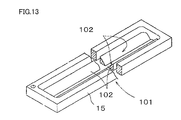
- Patent Document 1 Japanese Patent Laid-Open No. 2004-265978 (Patent Document 1) shown in FIG. 13 discloses a mounting substrate, a plurality of LEDs arranged in a line on the mounting substrate, and a mounting substrate so as to surround the LEDs.
- positioned in is disclosed.
- the phosphor resin is applied linearly and uniformly with high accuracy. It will be necessary. In order to realize this, one solution is that the concentration of the phosphor resin is not biased with the movement of the nozzle that discharges the phosphor resin when the phosphor resin is applied.
- Patent Document 2 Japanese Patent Application Laid-Open No. 2011-61056 (Patent Document 2) shown in FIG. 14 has a problem that a substrate is warped due to stress generated due to a difference in thermal expansion coefficient between a heat dissipation substrate and a circuit substrate during heat treatment.
- Patent Document 2 a linear light source module in which a light emitting element chip and a circuit chip are electrically connected in series by bonding wires is disclosed. Since an integrally formed substrate is used in place of different components pasted with a conventional adhesive, stress due to the difference in thermal expansion coefficient does not occur, and warping does not occur. As a result, the linear light source device becomes smaller, and it becomes easier to apply the phosphor resin linearly and uniformly with high accuracy.
- a reflector that extends along both sides of the light-emitting diode array is formed, and the reflector reflects light from the lateral side surface or the front surface of the light-emitting diode element. Illuminance can be obtained.
- the linear light source module is increased in size, and the light uniformity of the linear light source is likely to be biased due to the positional accuracy of the reflector, and the cost of the reflector is necessary and expensive.
- the inside of the frame is filled with a phosphor resin, and the phosphor resin often contains phosphor particles.
- the light emitted from the light emitting element is emitted more efficiently toward the outside by the phosphor particles.
- Patent Document 2 when the LED chip and the circuit chip are directly connected by bonding wires, the LED chip and the circuit chip are arranged in the wire forming direction.
- it is required to further reduce the size of the linear light source.
- the present invention has been made to solve the above-described problems, and in a linear light source module in which a plurality of light emitting elements are arranged on a mounting substrate, a linear light source module that improves uneven density of phosphors, and An object of the present invention is to provide a mounting substrate used for this and a method for manufacturing a linear light source module.
- a linear light source module is used for a linear light source module in which a plurality of light emitting elements are linearly mounted, and has a terminal portion for connecting an anode terminal and a cathode terminal of the linear light source. It is characterized by that.
- a linear light source module is used for a linear light source module in which a plurality of light emitting elements are linearly mounted, and an anode terminal and a cathode terminal of the linear light source are temporarily electrically connected. It is characterized by being connected.
- the anode terminal and the cathode terminal may be formed on a mounting substrate, or may be formed on a component of the linear light source module other than the mounting substrate.
- a plurality of linear light sources placed on the mounting board are temporarily connected to the anode terminal and the cathode terminal by wire bonding. It is preferable.
- a plurality of linear light sources placed on the mounting substrate are temporarily connected to the anode terminal and the cathode terminal electrically with solder. Preferably it is.
- the interval between the anode terminal and the cathode terminal placed on the mounting substrate is 4 mm or less.
- the method of manufacturing a linear light source module according to the present invention includes a short-circuit process for short-circuiting the anode terminal and the cathode terminal of the mounting substrate, and removing an electrical connection short-circuited in the short-circuit process.
- a short-circuit removing step is a short-circuit process for short-circuiting the anode terminal and the cathode terminal of the mounting substrate, and removing an electrical connection short-circuited in the short-circuit process.
- the linear light source module capable of improving the density unevenness of the phosphor resin, the mounting substrate used therefor, and the manufacturing method thereof I will provide a.
- linear light source module incorporated in a backlight of a liquid crystal display device, an illuminating device, an alternative illumination to a future fluorescent lamp, or the like.
- a light guide means such as a light guide is separately provided on the light exit surface side of the backlight of the liquid crystal display device.
- FIG. 1 is a perspective view partially showing a linear light source module according to Embodiment 1 of the present invention.
- FIG. 2 is a plan view showing the linear light source module in FIG.
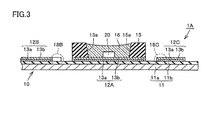
- FIG. 3 is a cross-sectional view showing the linear light source module in FIG.
- FIG. 3 shows a cross section of the linear light source module along the line III-III in FIG.
- the linear light source module 1 ⁇ / b> A mainly includes a mounting substrate 10, a frame body 15, and a plurality of LEDs 20.
- the mounting substrate 10 is made of a plate-like member having a rectangular shape in plan view, and includes a base material portion 11, a first conductive pattern 12A, and a pair of second conductive patterns 12B and 12C.
- the main surface of the mounting substrate 10 is roughly divided into a light source area where the frame body 15 and the plurality of LEDs 20 are mounted, and a peripheral area where other circuit components are mounted.
- the first conductive pattern 12A is provided so as to be disposed at a substantially central portion in the light source area, and at least a part of the pair of second conductive patterns 12B and 12C is disposed at the peripheral portion in the light source area. It is provided so that.
- the base material portion 11 includes a base 11a and an insulating layer 11b formed on the base 11a.
- the base 11a has high thermal conductivity such as aluminum from the viewpoint of efficiently dissipating heat generated by driving the LED 20 and heat generated in other circuit components mounted on the mounting substrate 10 to the outside. It is preferable to be comprised with the metal plate.
- the base 11a is not limited to this, and may be composed of a glass epoxy plate or a ceramic plate.
- the insulating layer 11b may be made of any material as long as insulation between the base 11a and the first and second conductive patterns 12A to 12C can be ensured.
- the base 11a is comprised with an insulator like the above-mentioned glass epoxy board or a ceramic board, formation of the insulating layer 11b is unnecessary.
- the first conductive pattern 12 ⁇ / b> A and the second conductive patterns 12 ⁇ / b> B and 12 ⁇ / b> C described above are formed on the main surface of the base material portion 11 (that is, on the main surface of the insulating layer 11 b). ing.
- the first conductive pattern 12A is a conductive pattern on which a plurality of LEDs 20 are mounted.
- the pair of second conductive patterns 12 ⁇ / b> B and 12 ⁇ / b> C is a conductive pattern including an alignment portion serving as an alignment mark for determining the mounting position of each of the plurality of LEDs 20.
- the reason why the plurality of LEDs 20 are mounted on the conductive pattern is mainly to efficiently dissipate heat generated by driving the LEDs 20 to the base material portion 11.
- each of the first conductive pattern 12A and the second conductive patterns 12B and 12C is formed so as to cover the wiring layer 13a formed on the main surface of the base member 11 and the wiring layer 13a. And the plated layer 13b.
- the first conductive pattern 12A and the second conductive pattern 12C do not have a function as wiring for transmitting an electric signal, and transmit the electric signal. This corresponds to a so-called dummy wiring formed simultaneously with other wiring layers.
- the layer 13a included in the first conductive pattern 12A and the second conductive pattern 12C is also referred to as a wiring layer.
- the material of the wiring layer 13a and the plating layer 13b is not particularly limited, but the wiring layer 13a is preferably made of a metal material such as copper from the viewpoint of thermal conductivity and conductivity.
- the layer 13b is preferably made of a metal material such as silver, aluminum, or platinum from the viewpoints of thermal conductivity, conductivity, and reflectance.
- a metal material such as silver, aluminum, or platinum from the viewpoints of thermal conductivity, conductivity, and reflectance.
- the thickness of the wiring layer 13a is preferably formed so that the cross-sectional area of the wiring layer 13a is as large as possible from the viewpoint of easy heat release and current flow.
- the thickness of the wiring layer 13a is preferably set to 0.035 mm or less.
- the first conductive pattern 12A is viewed from the normal direction of the main surface of the base material portion 11 (hereinafter, also simply referred to as “when viewed in plan”). It has a long, substantially rectangular shape.
- the LEDs 20 are linearly mounted on the first conductive pattern 12A along the direction in which the first conductive pattern 12A extends.
- the second conductive pattern 12B which is one of the pair of second conductive patterns 12B and 12C, is on the main surface of the base member 11 on the one side in the direction intersecting the direction in which the first conductive pattern 12A extends. It is provided so as to run in parallel with one conductive pattern 12A.
- the second conductive pattern 12B includes a base portion 12b extending along the direction in which the first conductive pattern 12A extends, and a plurality of convex portions protruding from the base portion 12b toward the first conductive pattern 12A. And an alignment unit 18B.
- the plurality of alignment portions 18B are spaced apart from each other with a certain distance along the direction in which the base portion 12b extends.
- the second conductive pattern 12C which is the other of the pair of second conductive patterns 12B and 12C, is on the other surface in the direction intersecting with the direction in which the first conductive pattern 12A extends on the main surface of the base 11. It is provided so as to run in parallel with one conductive pattern 12A.
- the second conductive pattern 12C includes a base portion 12c extending along a direction in which the first conductive pattern 12A extends and a plurality of convex portions protruding from the base portion 12c toward the first conductive pattern 12A side. And an alignment portion 18C.
- the plurality of alignment portions 18C are provided apart from each other at a certain distance along the direction in which the base portion 12c extends.
- the pair of second conductive patterns 12B and 12C are positioned on the main surface of the base member 11 so as to sandwich the first conductive pattern 12A along the direction intersecting with the direction in which the first conductive pattern 12A extends. become.
- the alignment portions 18B and 18C are provided so as to be alternately arranged along the direction in which the first conductive pattern 12A extends.
- each of the alignment portions 18B and 18C composed of a plurality of convex portions has a pair of corner portions when viewed in plan, and each or one of the pair of corner portions is an alignment corner portion for alignment.
- a plurality of alignment protruding corners formed by the corners of the protrusions intersect the direction in which the first conductive pattern 12 ⁇ / b> A extends on the main surface of the base material part 11.
- the first conductive pattern 12 ⁇ / b> A is disposed to face the first conductive pattern 12 ⁇ / b> A.
- the plurality of LEDs 20 correspond to light emitting elements that emit light when driven, and have a predetermined distance from each other in a line along the direction in which the first conductive pattern 12A extends as described above. It is mounted on the pattern 12A. More specifically, each of the plurality of LEDs 20 is bonded to the first conductive pattern 12A by a die bond material (not shown). Adjacent LEDs of the plurality of LEDs 20 are electrically connected by a bonding wire 21 made of a gold wire or the like.
- the frame body 15 is formed of, for example, a white resin molded body, and is preferably integrated with the mounting substrate 10 by injection molding (outsert molding). Formed.
- the frame 15 is formed in a shape having a slit-like internal hollow so that its outer shape is annular (frame shape), and is disposed along the periphery of the first conductive pattern 12A described above.
- the frame body 15 is provided so as to surround the plurality of LEDs 20 arranged in the above-described line shape.
- the frame 15 has a reflection surface 15 a that reflects a part of the light emitted from the plurality of LEDs 20 on the inner peripheral portion thereof.
- the reflection surface 15a is preferably provided in an inclined shape as shown in FIG. With this configuration, when the LED 20 is driven, the light reflected by the reflecting surface 15a can be guided in the optical axis direction of the LED 20, and light is efficiently emitted toward the outside. .
- the hollow inside of the frame 15 is filled with a phosphor resin 16.
- the phosphor resin 16 is made of, for example, a silicone resin or an epoxy resin, and seals the plurality of LEDs 20 positioned inside the frame-like reflector 15.
- the phosphor resin 16 has phosphor particles dispersed therein.
- the insulating layer 11b is formed on the base 11a, and the wiring layer 13a is further formed on the formed insulating layer 11b.
- the insulating layer 11b is formed on the base 11a by, for example, adhesion or vapor deposition.
- the wiring layer 13a is insulated by performing an etching process using a photomask on the conductor layer and patterning it into a predetermined shape. It is formed on the layer 11b.
- a plating layer 13b is formed on the wiring layer 13a. More specifically, a work-in-process product in which a wiring layer 13a patterned in a predetermined shape is formed on the main surface of the base member 11 is immersed in a plating solution, and a voltage is applied to the wiring layer 13a while maintaining the state. By applying, the surface of the exposed wiring layer 13a is plated. Thereby, the plating layer 13b is formed on the wiring layer 13a. In this way, the mounting substrate 10 in which the first conductive pattern 12A and the second conductive patterns 12B and 12C are formed on the main surface of the base member 11 is manufactured.
- the edge of the formed wiring layer 13a is rounded.
- the roundness of the edge portion appears rounded at the edge portion of the plating layer 13b during the subsequent plating process, and as a result, the edge portions of the first conductive pattern 12A and the second conductive patterns 12B and 12C. Will be rounded.
- the wiring layer 13a is formed to be thicker than necessary as described above. It is important not to.
- the frame body 15 is formed on the main surface side of the mounting substrate 10. More specifically, the frame body 15 is formed on the first conductive pattern 12A by placing the mounting substrate 10 on the molding die of the injection molding apparatus, pouring white resin into the molding die, and curing the white resin. By forming the frame 15 on the mounting substrate 10 by injection molding in this way, the mounting position of the frame 15 on the mounting substrate 10 is positioned with high accuracy.
- the plurality of LEDs 20 are positioned and mounted on the first conductive pattern 12A. More specifically, the mounting positions of each of the plurality of LEDs 20 are determined based on the alignment portion included in the second conductive patterns 12B and 12C described above, and based on this, the plurality of LEDs 20 are first connected using a chip mounter or the like. It is mounted on one conductive pattern 12A. Thereafter, the plurality of LEDs 20 are wire-bonded using the bonding wires 21 and further sealed with the phosphor resin 16, whereby the linear light source module 1A as shown in FIGS. 1 to 3 is completed.
- FIG. 4 is a conceptual diagram for explaining a phosphor resin coating process. While discharging a predetermined amount of the phosphor resin from the tip of the dispenser nozzle 23, the tip of the nozzle is moved from the anode terminal side ( ⁇ terminal) to the cathode terminal side (+ terminal) on the first conductive pattern 12A to make it uniform. A phosphor resin is applied to the surface.
- FIG. 5 is a graph showing the relationship between the application position of the linear light source module 1A and the chromaticity y distribution by conventional phosphor resin application.
- the chromaticity y distribution from the anode terminal ( ⁇ terminal) to the cathode terminal (+ terminal) is about 0.15 in the vicinity of the anode terminal ( ⁇ terminal). It rises as it approaches (terminal) and reaches about 0.2 near the cathode terminal (+ terminal). For this reason, the chromaticity y is biased in the linear light source module 1A, and the irradiance distribution of the light emitted from the plurality of LEDs 20 is uneven. As described in a verification experiment described later, this is considered to be an influence of charging of the phosphor particles contained in the phosphor resin.
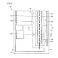
- FIG. 6 is a plan view showing the entire linear light source module in FIG.
- the cathode terminal (+ terminal) on the second conductive pattern 12B and the anode terminal ( ⁇ terminal) on the third conductive pattern 12D are wire-bonded using a bonding wire 21.
- the plurality of LEDs 20 are formed on the first conductive pattern 12A at intervals of a chip pitch of 1.00 to 2.00 mm (preferably around 1.6 mm).
- a cluster 22 of linear light source modules is formed by connecting about 15 LEDs 20 in series with bonding wires. Further, the interval between the clusters 22 is 3.00 to 4.00 mm (preferably around 3.7 mm), and approximately four clusters are formed in one linear light source module 1A.
- the phosphor resin shown in FIG. 4 is thermally cured, and the wire is formed at the terminal portion between the anode terminal ( ⁇ terminal) and the cathode terminal (+ terminal) until the predetermined treatment is completed. It is possible to bond.
- the phosphor particles are charged to the anode ( ⁇ ) when the phosphor resin is applied, and have the property of being easily collected at the cathode terminal (+ terminal). Yes.
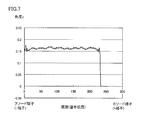
- FIG. 7 is a graph showing the relationship between the application position of the linear light source module 1A and the chromaticity y distribution by applying the phosphor resin in the present embodiment.
- the chromaticity y is about 0.17 in the vicinity of the anode terminal ( ⁇ terminal), and is also about 0.17 when approaching the cathode terminal (+ terminal), and the linear light source module 1A.
- the chromaticity bias is not confirmed.
- the irradiance distribution of the light emitted from the plurality of LEDs 20 is improved to be uniform with high accuracy.
- FIG. 8 is a plan view showing the entire linear light source module according to Embodiment 2 of the present invention.
- the linear light source module 1B in the present embodiment will be described with reference to FIG.
- the terminal positions and connection methods of the anode terminal ( ⁇ terminal) and the cathode terminal (+ terminal) described in Embodiment 1 are different. That is, in the linear light source module 1B of the present embodiment, a + terminal portion is formed by connecting the anode terminals of all clusters, and similarly, a-terminal portion is formed by connecting the cathode terminals of all clusters.
- the + terminal part and the-terminal part are short-circuited by solder. Thereby, the burden of the manufacturing method called the short circuit and cutting
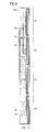
- FIG. 9 is a wiring diagram of an actual product substrate of the linear light source module.
- the mounting board of the linear light source module is composed of a plate-like member having a rectangular shape in plan view and having a width of about 10 mm and a length of about 110 mm.
- a light source area where the reference hole, the frame body 15 and the plurality of LEDs 20 are mounted, and a peripheral area where other circuit components are mounted are arranged.
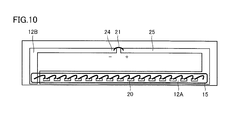
- FIG. 10 is a conceptual diagram of a method for manufacturing a linear light source module, a mounting substrate, and a linear light source module.
- the configuration of the present invention has been described in the form of an actual product with reference to FIGS. 6, 8, and 9. Subsequently, referring to FIG. 10, the linear light source module to which the present invention is applied, and the mounting The concept of the method for manufacturing the substrate and the linear light source module will be described.
- a plurality of LEDs 20 are connected by bonding wires, and the linear light source module has an anode terminal ( ⁇ terminal) 24 and a cathode terminal (+ terminal) 25 in a wiring area wired with the LEDs 20.
- the anode terminal ( ⁇ terminal) 24 and the cathode terminal (+ terminal) 25 are short-circuited before the phosphor resin coating process, and removed by some method after the phosphor resin coating process, for example, disconnection of the bonding wire or etching of the wiring. Disconnect the anode terminal ( ⁇ terminal) and the cathode terminal (+ terminal).
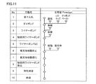
- FIG. 11 is a flowchart showing the steps of the method for manufacturing the linear light source module.
- the quality of the parts is checked in the acceptance inspection process, and the plurality of LEDs 20 are die-bonded to the first conductive pattern 12A in the die-bonding process.
- the bonding wire process the plurality of LEDs 20 are connected by bonding wires, and simultaneously or after that, the anode terminal ( ⁇ terminal) and the cathode terminal (+ terminal) are connected by bonding wires.
- the same processing is performed for the solder of the second embodiment.
- quality inspection of the bonding wire is performed in the bonding wire QC process, and the plurality of LEDs 20 in the frame body 15 are sealed with a predetermined phosphor resin in the phosphor resin coating process. After the sealed phosphor resin is cured by heat treatment, the bonding wire is disconnected or the solder is disconnected in a short-circuit bonding wire process.
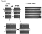
- FIG. 12 is a photograph showing the result of the verification experiment.
- a comb-tooth pattern of copper wiring of a wiring sheet (copper foil thickness 35 ⁇ m, wiring 1.5 mm pitch product) on a glass plate is prepared, and a phosphor resin is applied on the pattern in the same manner. Experiments were performed. As a result, it was confirmed that the phosphor resin gathered on the cathode terminal (+ terminal) side, and the phosphor particles in the phosphor resin were charged on the anode ( ⁇ ).
- the movement of the phosphor particles from the initial stage of the comb pattern of the copper wiring is shown by a micrograph, and the phosphor particles are charged on the anode ( ⁇ ) even in the moving picture of the entire photograph. I have confirmed that.
- the frame 15 is integrated with the mounting substrate 10 by outsert molding.
- the frame 15 is attached to the mounting substrate 10 using other methods. It may be assembled.
- the linear meaning of the plurality of LEDs 20 refers to a certain direction such as a curved shape, a parallel shape, a zigzag shape, a rectangular shape, or a square shape. It is not limited to what was arranged.
- the present invention can be used as a linear light source module and a mounting substrate.
- 1A to 1C linear light source module 10 mounting substrate, 11 base part, 11a base, 11b insulating layer, 12A first conductive pattern, 12B second conductive pattern, 12C second conductive pattern, 12D third conductive pattern, 12b base Part, 12c base part, 13a wiring layer, 13b plating layer, 14 white resist film, 15 frame, 15a reflecting surface, 16 phosphor resin, 18B alignment part, 18C alignment part, 20 LED, 21 bonding wire, 22 cluster, 23 dispenser nozzle, 24 anode terminal (-terminal), 25 cathode terminal (+ terminal), 26 solder, 101 linear light source, 102 reflector, 103 circuit chip.
Landscapes
- Led Device Packages (AREA)
- Non-Portable Lighting Devices Or Systems Thereof (AREA)
Abstract
実装基板(10)上のアノード端子(24)およびカソード端子(25)間でワイヤボンドもしくははんだ接続することによって、蛍光体樹脂中に含まれる蛍光体粒子の帯電による色度の偏りを防止し、さらには、複数のLED(20)から出射される光の放射照度分布にむらを改善することができる。さらに、端子接続部でワイヤボンドを切断することによって、電気的な接続が分離された本来の配線状態に戻すことも可能となる。このような構成により、複数の発光素子を実装基板上に配置した線状光源モジュールにおいて、蛍光体樹脂の濃度むらを改善することができる線状光源モジュール、これに用いられる実装基板および線状光源モジュールの製造方法を提供する。
Description
本発明は、複数の発光素子が実装基板上に線状に実装されてなる線状光源モジュール、実装基板および線状光源モジュールの製造方法に関する。
従来、各種表示装置や照明装置等に使用される光源モジュールとして、線状光源モジュールが知られている。線状光源モジュールは、LED(Light Emitting Diode)等の発光素子を線状に配置してなる光源モジュールである。
当該線状光源モジュールにおいては、線状に配置された複数の発光素子から出射された光が導光板等の導光手段に効率よく入射されるように、当該複数の発光素子を取り囲むように枠体が設けられる場合が多い。
たとえば、図13に示す特開2004-265978号公報(特許文献1)には、実装基板と、当該実装基板上に線状に配置された複数のLEDと、当該LEDを取り囲むように実装基板上に配置された枠体および反射体とを備えた線状光源モジュールが開示されている。
この種の線状光源モジュールにおいては、出射される光の放射照度分布にむらが生じることを抑制することが重要であり、そのためには、蛍光体樹脂を線状かつ均一に高精度に塗布することが必要になる。これを実現するためには、蛍光体樹脂の塗布時に、蛍光体樹脂を放出するノズルの移動に伴って蛍光体樹脂の濃度に偏りを生じないことが一つの解決方法となる。
また、たとえば、図14に示す特開2011-61056号公報(特許文献2)には、熱処理時の放熱基板と回路基板との熱膨張係数の差により応力が発生して基板が反るという課題に対して、発光素子チップおよび回路チップをボンディングワイヤによって電気的に直列接続する線状光源モジュールが開示されている。従来の接着剤で貼り付けた異なる部品の代りに、一体形成された基板を用いているので、熱膨張係数の差による応力が生じず、反りは生じない。その結果として、線状光源装置は小型になり、より蛍光体樹脂を線状かつ均一に高精度に塗布しやすくなる。
上述した特許文献1に開示されるように、発光ダイオードアレイの両側に沿って延びる反射体を形成し、この反射体により発光ダイオード素子の横側面または前面からの光を反射することによって、より高い照度を得ることができる。しかしながら、線状光源モジュールとしては大型化してしまい、反射体の位置精度により線状光源の光の均一性について偏りが生じやすく、コスト的にも反射体の費用が必要となり高価になる。
そこで、線状光源モジュールにあっては、枠体の中を蛍光体樹脂で充填し、蛍光体樹脂中には蛍光体粒子が含有される場合が多い。一般的な構成として、発光素子から出射された光はこの蛍光体粒子により、外部に向けてより効率的に出射される。また、上述した特許文献2に開示されるように、LEDチップと回路チップとを直接ボンディングワイヤにより接続すれば、ワイヤの形成方向にLEDチップおよび回路チップが配置される。しかしながら、出射される光の放射照度の分布むらをさらに低減させるためには、線状光源をさらに小型化することが求められる。
そこで、各LEDチップのみを直接ボンディングワイヤで接続することによって、線状方向により小型に配置する手法が考えられる。しかしながら、たとえばディスペンサを使用して蛍光体樹脂を枠体中に塗布した場合、蛍光体樹脂の硬化後に何らかの作用により、線状方向に蛍光体の濃度むらが生じる場合がある。そして、蛍光体の濃度むらは、線状光源自体の出射される光の放射照度分布にむらに繋がる結果となっている。
したがって、本発明は、上述した問題点を解決すべくなされたものであり、複数の発光素子を実装基板上に配置した線状光源モジュールにおいて、蛍光体の濃度むらを改善する線状光源モジュールと、これに用いられる実装基板と、線状光源モジュールの製造方法とを提供することを目的とする。
本発明に基づく線状光源モジュールは、複数の発光素子が線状に実装されてなる線状光源モジュールに用いられるものであって、線状光源のアノード端子およびカソード端子を接続させる端子部を有することを特徴とする。
本発明に基づく線状光源モジュールは、複数の発光素子が線状に実装されてなる線状光源モジュールに用いられるものであって、線状光源のアノード端子およびカソード端子を一時的に電気的に接続させることを特徴とする。
上記アノード端子および上記カソード端子は、実装基板上に形成されていてもよいし、実装基板以外の線状光源モジュールの構成部品上に形成されてもよい。
上記本発明に基づく上記実装基板にあっては、上記実装基板上に載置した複数の線状光源を、一時的に上記アノード端子および上記カソード端子をワイヤボンドで電気的に接続して構成されていることが好ましい。
上記本発明に基づく上記実装基板にあっては、上記実装基板上に載置した複数の線状光源を、一時的に上記アノード端子および上記カソード端子をはんだで電気的に接続して構成されていることが好ましい。
上記本発明に基づく上記実装基板にあっては、上記実装基板上に載置したアノード端子およびカソード端子の端子間隔を4mm以下になるように形成されていることが好ましい。
上記本発明に基づく線状光源モジュール製造方法は、上記実装基板の上記アノード端子と上記カソード端子とを短絡させるための短絡工程と、上記短絡工程で短絡させた電気的な接続を除去するための短絡部除去工程とを含むことを特徴とする。
本発明によれば、複数の発光素子を実装基板上に配置した線状光源モジュールにおいて、蛍光体樹脂の濃度むらを改善することができる線状光源モジュールおよびこれに用いられる実装基板とその製造方法を提供する。
(実施の形態1)
以下、本発明の実施の形態について、図を参照して詳細に説明する。
以下、本発明の実施の形態について、図を参照して詳細に説明する。
以下に示す実施の形態は、いずれも、液晶表示装置のバックライト、照明装置、今後の蛍光灯への代替え照明等に組み込まれる線状光源モジュールを例示するものである。当該線状光源モジュールは、ここではその説明を省略するが、液晶表示装置のバックライトでは、その出射面側に導光体等の導光手段が別途設置されることを前提とする。
なお、以下に示す実施の形態においては、同様のまたは共通する部分について図中同一の符号を付し、その説明は繰り返さない。
図1は、この発明の実施の形態1における線状光源モジュールを部分的に示す斜視図である。図2は、図1中の線状光源モジュールを示す平面図である。図3は、図1中の線状光源モジュールを示す断面図である。図3中には、図2中のIII-III線上に沿った線状光源モジュールの断面が示されている。
まず、これら図1から図3を参照して、本実施の形態における線状光源モジュール1Aの構造について説明する。
図1から図3に示すように、本実施の形態における線状光源モジュール1Aは、実装基板10と、枠体15と、複数のLED20とを、主として備えている。
実装基板10は、平面視矩形状の板状の部材からなり、基材部11と、第1導電パターン12Aと、一対の第2導電パターン12B,12Cとを有している。当該実装基板10の主表面は、枠体15および複数のLED20が実装される光源エリアと、他の回路部品が実装される周辺エリアとに大別される。第1導電パターン12Aは、光源エリア内の略中央部に配置されるように設けられており、一対の第2導電パターン12B,12Cは、少なくともその一部が光源エリア内の周縁部に配置されるように設けられている。
図1および図3に示すように、基材部11は、ベース11aと、当該ベース11a上に形成された絶縁層11bとを含んでいる。ベース11aは、LED20が駆動することで生じた熱や、実装基板10に実装された他の回路部品にて生じた熱を、外部に効率的に放熱する観点から、アルミニウム等の高熱伝導性の金属板にて構成されていることが好ましい。しかしながら、ベース11aは、これに限定されるものではなく、ガラスエポキシ板や、セラミックス板にて構成されていてもよい。また、絶縁層11bは、ベース11aと第1および第2導電パターン12A~12Cとの間の絶縁性が確保できるものであれば、どのような材質のものであってもよい。なお、ベース11aを、上述したようなガラスエポキシ板やセラミックス板の如くの絶縁体にて構成した場合には、絶縁層11bの形成は不要である。
図1から図3に示すように、基材部11の主表面上(すなわち、絶縁層11bの主表面上)には、上述した第1導電パターン12Aおよび第2導電パターン12B,12Cが形成されている。第1導電パターン12Aは、その表面上に複数のLED20が実装される導電パターンである。一対の第2導電パターン12B,12Cは、複数のLED20の各々の実装位置を決定するためのアラインメントマークとなるアラインメント部を含む導電パターンである。なお、本実施の形態において、複数のLED20が導電パターン上に実装される理由は、主として、LED20が駆動することで生じた熱を基材部11に効率的に放熱するためである。
図3に示すように、第1導電パターン12Aおよび第2導電パターン12B,12Cのそれぞれは、基材部11の主表面上に形成された配線層13aと、当該配線層13aを覆うように形成されためっき層13bとを含んでいる。なお、本実施の形態における線状光源モジュール1Aにあっては、第1導電パターン12Aおよび第2導電パターン12Cは、電気信号を伝送するための配線としての機能を有せず、電気信号を伝送するための他の配線層と同時に形成されるいわゆるダミー配線に相当するものである。しかしながら、ここでは、これら第1導電パターン12Aおよび第2導電パターン12Cに含まれる層13aについても配線層と称している。
配線層13aおよびめっき層13bの材質は、特に限定されるものではないが、配線層13aは、熱伝導率および導電率の観点から銅などの金属材料にて構成されていることが好ましく、めっき層13bは、熱伝導率、導電率および反射率の観点から、銀、アルミニウム、白金などの金属材料にて構成されていることが好ましい。なお、光が実装基板10に一切照射されないように構成されている場合や、配線層13aの腐食を防止するために別途プリフラックスを配線層13aに塗布する場合等には、めっき層13bの形成は不要である。
配線層13aの厚みとしては、熱の逃がし易さや電流の流れ易さ等の観点から、配線層13aの断面積ができるだけ大きくなるように厚く形成することが好ましい。
しかしながら、配線層13aの厚みが大きすぎる場合には、配線層13aのパターニングの際に、不要部分を溶解させるために大量のエッチング液が必要になるとともに、エッチングのタクトタイムも長時間化する。このため、これらを考慮して配線層13aを最適な厚みとすることが好ましい。また、配線層13aの厚みが大きすぎる場合には、後述するアラインメント部のエッジ部に大きな丸みが生じてしまう原因になる。このため、上述した各種の観点から、配線層13aの厚みとしては、0.035mm以下とされることが好ましい。
図1および図2に示すように、第1導電パターン12Aは、基材部11の主表面の法線方向から見た場合に(以下、単にこれを「平面視した場合に」とも称する)、長尺の略矩形状の形状を有する。第1導電パターン12Aには、第1導電パターン12Aが延びる方向に沿ってLED20が線状に実装されている。
一対の第2導電パターン12B,12Cのうちの一方である第2導電パターン12Bは、基材部11の主表面上において、第1導電パターン12Aの延びる方向と交差する方向の一方側で当該第1導電パターン12Aと概ね並走するように設けられている。
より詳細には、第2導電パターン12Bは、第1導電パターン12Aが延びる方向に沿って延びるベース部12bと、当該ベース部12bから第1導電パターン12A側に向けて突出する複数の凸部からなるアラインメント部18Bとを含んでいる。当該複数のアラインメント部18Bは、ベース部12bが延びる方向に沿って一定の距離を有して、互いに離間して設けられている。
一対の第2導電パターン12B,12Cのうちの他方である第2導電パターン12Cは、基材部11の主表面上において、第1導電パターン12Aの延びる方向と交差する方向の他方側で当該第1導電パターン12Aと概ね並走するように設けられている。
より詳細には、第2導電パターン12Cは、第1導電パターン12Aが延びる方向に沿って延びるベース部12cと、当該ベース部12cから第1導電パターン12A側に向けて突出する複数の凸部からなるアラインメント部18Cとを含んでいる。当該複数のアラインメント部18Cは、ベース部12cが延びる方向に沿って一定の距離を有して、互いに離間して設けられている。
以上により、一対の第2導電パターン12B,12Cは、基材部11の主表面上において第1導電パターン12Aが延びる方向と交差する方向に沿って第1導電パターン12Aを挟み込むように位置することになる。なお、アラインメント部18B,18Cは、第1導電パターン12Aが延びる方向に沿って互い違いに配置されるように設けられている。
ここで、複数の凸部からなるアラインメント部18B,18Cのそれぞれは、平面視した場合に一対の角部を有しており、これら一対の角部の各々または一方がアラインメント用の出隅部となる。すなわち、上記構成を採用することにより、凸部の角部にて構成される複数のアラインメント用の出隅部が、基材部11の主表面上において、第1導電パターン12Aが延びる方向と交差する方向に沿って当該第1導電パターン12Aに対峙して配置されることになる。
複数のLED20は、駆動されることで光を出射する発光素子に該当し、上述したように第1導電パターン12Aの延びる方向に沿って線状に互いに所定の距離を有して、第1導電パターン12A上に実装されている。より詳細には、複数のLED20の各々は、図示しないダイボンド材によって第1導電パターン12Aに接着されている。複数のLED20のうちの隣り合うLED同士は、金線等からなるボンディングワイヤ21によって電気的に接続されている。
図1から図3に示すように、枠体15は、たとえば白色樹脂の成形体にて構成されており、好適には、射出成形(アウトサート成形)されることによって実装基板10に一体化させて形成される。枠体15は、その外形が環状(額縁状)となるようにスリット状の内部中空を有する形状に形成されており、上述した第1導電パターン12Aの周縁に沿って配設されている。
枠体15は、上述した線状に配置された複数のLED20を取り囲むように設けられている。枠体15は、当該複数のLED20から出射された光の一部を反射する反射面15aをその内周部に有している。なお、当該反射面15aは、図3に示すように傾斜状に設けられることが好ましい。このように構成することにより、LED20の駆動時において、反射面15aで反射された光をLED20の光軸方向に導くことが可能になり、外部に向けて効率よく光が出射されることになる。
また、図3に示すように、枠体15の内部中空には、蛍光体樹脂16が充填されている。蛍光体樹脂16は、たとえばシリコーン樹脂やエポキシ樹脂等からなり、枠状の反射体15の内部中空に位置決めされた複数のLED20を封止している。なお、蛍光体樹脂16には、蛍光体粒子が分散配置されている。
次に、本実施の形態における線状光源モジュール1Aを製造するための具体的な製造方法について説明する。
本実施の形態における線状光源モジュール1Aを製造するに際しては、まずベース11a上に絶縁層11bを形成し、形成した絶縁層11b上にさらに配線層13aを形成する。具体的には、絶縁層11bは、たとえば接着や蒸着等によってベース11a上に形成される。配線層13aは、蒸着または接着等によって絶縁層11b上に導体層が形成された後に、当該導体層に対してフォトマスクを用いたエッチング処理が行なわれて所定形状にパターニングされることにより、絶縁層11b上に形成される。
次に、配線層13a上にめっき層13bを形成する。より詳細には、所定形状にパターニングされた配線層13aが基材部11の主表面上に形成されてなる仕掛品を、めっき液に浸漬し、当該状態を維持しつつ配線層13aに電圧を印加することにより、剥き出しとなっている配線層13aの表面にめっき処理を施す。これにより、めっき層13bが配線層13a上に形成される。以上により、第1導電パターン12Aおよび第2導電パターン12B,12Cが基材部11の主表面上に形成されてなる実装基板10が製作される。
なお、上述したエッチング処理の際には、形成される配線層13aのエッジ部に丸みが生じてしまうことになる。当該エッジ部の丸みは、その後に行なわれるめっき処理の際にもめっき層13bのエッジ部に丸みとなって現れるため、結果的に第1導電パターン12Aおよび第2導電パターン12B,12Cのエッジ部に丸みが生じてしまうことになる。
このため、第2導電パターン12B,12Cに含まれるアラインメント部のエッジ部に丸みが可能な限り生じないようにするためには、前述したように配線層13aの厚みを必要以上に厚く形成し過ぎないことが重要である。
次に、実装基板10の主表面側に枠体15を形成する。より詳細には、実装基板10を射出成形装置の成形型に設置した後、白色樹脂を成形型に流し込み、これを硬化させることによって、第1導電パターン12A上に枠体15が形成される。なお、このように枠体15を実装基板10に対して射出成形にて形成することにより、実装基板10に対する枠体15の実装位置が高精度に位置決めされることになる。
次に、第1導電パターン12A上に複数のLED20が位置決めして実装される。より詳細には、上述した第2導電パターン12B,12Cに含まれるアラインメント部を基準として、複数のLED20の各々の実装位置が決定され、これに基づいて複数のLED20がチップマウンタ等を用いて第1導電パターン12A上に実装される。その後、複数のLED20がボンディングワイヤ21を用いてワイヤボンドされ、さらに蛍光体樹脂16によって封止されることにより、図1から図3に示した如くの線状光源モジュール1Aが完成する。
図4は、蛍光体樹脂の塗布工程を説明するための概念図である。ディスペンサノズル23の先端から出た蛍光体樹脂を一定量ずつ放出しながら、第1導電パターン12A上のアノード端子側(-端子)からカソード端子側(+端子)までノズル先端を移動させて、均一に蛍光体樹脂を塗布する。
図5は、従来の蛍光体樹脂塗布による、線状光源モジュール1Aの塗布位置と色度y分布との関係を示すグラフである。アノード端子(-端子)を原点として、カソード端子(+端子)までの色度y分布は、図に示されるように、アノード端子(-端子)付近が0.15程度であり、カソード端子(+端子)に近づくにつれて上昇し、カソード端子(+端子)付近では、0.2程度に達している。このため、線状光源モジュール1A内に色度yの偏りが生じ、複数のLED20から出射される光の放射照度分布にむらを与えている。これは、後述する検証実験で記述するが、蛍光体樹脂中に含まれる蛍光体粒子の帯電による影響と考えられる。
図6は、図1中の線状光源モジュールの全体を示す平面図である。第2導電パターン12B上のカソード端子(+端子)および第3導電パターン12D上のアノード端子(-端子)が、ボンディングワイヤ21を用いてワイヤボンドされている。また、複数のLED20は、チップピッチ1.00~2.00mm(好ましくは1.6mm前後)の間隔で第1導電パターン12A上に形成されている。15個程度のLED20がボンディングワイヤで直列に接続されることによって、線状光源モジュールのクラスタ22が形成されている。さらに、クラスタ22の間隔は、3.00~4.00mm(好ましくは3.7mm前後)を有し、1つの線状光源モジュール1A内には、およそ4つのクラスタが形成されている。
これらのカソード端子(+端子)およびアノード端子(-端子)のワイヤボンドは、複数のLED20のワイヤボンドと同時に形成される。
そして、図4に示した蛍光体樹脂塗布後、蛍光体樹脂の熱硬化を行ない、所定の処理が完了するまでアノード端子(-端子)およびカソード端子(+端子)間の端子部にて、ワイヤボンドすることを可能とする。
一方で、蛍光体樹脂中に含まれる蛍光体粒子の帯電により、蛍光体樹脂塗布時に蛍光体粒子はアノード(-)に帯電しており、カソード端子(+端子)に集合しやすい特性を持っている。
このため、線状光源モジュール1A内に色度の偏りを生じやすくなっている。しかしながら、上述のアノード端子およびカソード端子間でワイヤボンドすることによって、アノード端子(-端子)およびカソード端子(+端子)が一時的に短絡された状態、つまり電位差が無くなった状態となる。
これにより、後の工程である蛍光体樹脂の熱硬化等によるカソード端子(+端子)への蛍光体粒子の集束促進を防止することができるようになる。さらに、蛍光体樹脂塗布、熱硬化等の後に、端子部のワイヤボンド部分を切断することによって、アノード端子(-端子)およびカソード端子(+端子)間の電気的な接続の分離が可能となる。
このアノード端子およびカソード端子間でワイヤボンドすることで、蛍光体樹脂中に含まれる蛍光体粒子の帯電による色度の偏りを防止し、さらには、複数のLED20から出射される光の放射照度分布にむらが生じることを改善できる。さらには、端子接続部でワイヤボンドを切断することで、電気的な接続が分離された本来の配線状態に戻すことも可能となる。
図7は、本実施の形態における蛍光体樹脂塗布による、線状光源モジュール1Aの塗布位置と色度y分布との関係を示すグラフである。図に示されるように、色度yはアノード端子(-端子)付近が0.17程度であり、カソード端子(+端子)に近づいても同様に0.17程度であり、線状光源モジュール1A内に色度yの偏りが確認されない。さらには、複数のLED20から出射される光の放射照度分布が、高精度に均一なものに改善される。
以上の結果より、本実施の形態における線状光源モジュール1Aによれば、LED20の色度yの偏りが減少するとともに、光の放射照度分布が従来例に対して改善することが確認された。したがって、本発明の有意な効果が当該結果により確認された。
(実施の形態2)
図8は、この発明の実施の形態2における線状光源モジュールの全体を示す平面図である。
図8は、この発明の実施の形態2における線状光源モジュールの全体を示す平面図である。
以下、この図8を参照して、本実施の形態における線状光源モジュール1Bについて説明する。この線状光源モジュール1Bについては、実施の形態1で記載したアノード端子(-端子)およびカソード端子(+端子)の端子位置および接続方法が相違する。すなわち、本実施の形態の線状光源モジュール1Bでは、全クラスタのアノード端子を連結させた+端子部を形成し、同様に全クラスタのカソード端子を連結させた-端子部を形成する。
+端子部および-端子部は、はんだによって短絡されている。これにより、1つの線状光源モジュールの微細なワイヤボンドでの短絡、切断という製造方法の負担を低減する。また、大きなはんだによる+端子部および-端子部の短絡箇所1カ所を、短絡、切断することによって、実施の形態1と同様に、線状光源モジュール内に色度の偏りがなく、さらには、複数のLED20から出射される光の放射照度分布が高精度に均一なものに改善された状態を実現することができる。
図9は、線状光源モジュールの実製品基板の配線図である。線状光源モジュールの実装基板は、幅10mm、長さ110mm程度の大きさの平面視矩形状の板状の部材から構成されている。実装基板10の主表面には、基準穴、枠体15および複数のLED20が実装される光源エリアと、他の回路部品が実装される周辺エリアとが配置されている。
図10は、線状光源モジュール、実装基板および線状光源モジュールの製造方法の概念図である。図6、図8および図9を参照して、本願発明の構成を実製品での形態で説明したが、引き続いて、図10を参照して、本発明が適用された線状光源モジュール、実装基板および線状光源モジュールの製造方法の概念について説明する。複数のLED20がボンディングワイヤで接続されており、線状光源モジュールは、そのLED20と配線された配線エリアに、アノード端子(-端子)24およびカソード端子(+端子)25を有する。アノード端子(-端子)24およびカソード端子(+端子)25を、蛍光体樹脂の塗布工程前に短絡し、蛍光体樹脂塗布工程後に何らかの方法、たとえば、ボンディングワイヤの断線、配線のエッチィングによる除去にて、アノード端子(-端子)とカソード端子(+端子)を断線する。
図11は、線状光源モジュールの製造方法の工程を示すフロー図である。受け入れ検査工程にて部品の品質確認を行ない、ダイボンド工程にて、複数のLED20を第1導電パターン12Aにダイボンドする。次に、ボンディングワイヤ工程にて、複数のLED20をボンディングワイヤで接続し、同時あるいはその後にアノード端子(-端子)およびカソード端子(+端子)をボンディングワイヤで接続する。なお、実施の形態2のはんだについても同様の処理で行なう。次に、ボンディングワイヤQC工程でボンディングワイヤの品質検査を行ない、蛍光体樹脂塗布工程にて、枠体15中の複数のLED20を所定の蛍光体樹脂で封止する。封止された蛍光体樹脂を熱処理により硬化した後、短絡用ボンディングワイヤ工程にて、ボンディングワイヤの断線、あるいははんだ断線を行う。
図12は、検証実験の結果を示す写真である。ガラス板上の配線シート(銅箔厚さ35μm、配線1.5mmピッチ品)の銅配線の櫛歯パターンを作成して、同様にパターン上に蛍光体樹脂を塗布し、線状光源モジュールの模式実験を実施した。その結果、カソード端子(+端子)側に蛍光体樹脂が集まり、蛍光体樹脂中の蛍光体粒子はアノード(-)に帯電していることを確認している。図12中には、銅配線の櫛歯パターンの初期から処理後における蛍光体粒子の移動の様子を顕微鏡写真にて示しており、全体写真の動画においても蛍光体粒子はアノード(-)に帯電していることを確認している。
なお、本実施の形態においては、枠体15がアウトサート成形によって実装基板10に一体化された場合を例示して説明を行なったが、他の方法を用いて枠体15を実装基板10に組み付けることとしてもよい。
さらに、複数のLED20の線状の意味は、湾曲状、並列状、ジグザグ状、長方形状、正方形状といった一定の方向性を指し、直線性が一部でもあれば、一直線にのみ複数のLED20が配列したものに限定されない。
このように、今回開示した上記実施の形態はすべての点で例示であって、制限的なものではない。本発明の技術的範囲は請求の範囲によって画定され、また請求の範囲の記載と均等の意味および範囲内でのすべての変更を含むものである。
本発明は、線状光源モジュールおよび実装基板として利用可能である。
1A~1C 線状光源モジュール、10 実装基板、11 基材部、11a ベース、11b 絶縁層、12A 第1導電パターン、12B 第2導電パターン、12C 第2導電パターン、12D 第3導電パターン、12b ベース部、12c ベース部、13a 配線層、13b めっき層、14 白色レジスト膜、15 枠体、15a 反射面、16 蛍光体樹脂、18B アラインメント部、18C アラインメント部、20 LED、21 ボンディングワイヤ、22 クラスタ、23 ディスペンサノズル、24 アノード端子 (-端子)、25 カソード端子(+端子)、26 はんだ、101 線状光源、102 反射体、103 回路チップ。
Claims (10)
- 複数の発光素子(20)が実装基板(10)上に線状に実装されてなる線状光源モジュールであって、
前記実装基板(10)の基材部(11)の主表面上に設けられ、複数の前記発光素子(20)がその表面上に実装された第1導電パターン(12A)と、
前記基材部(11)の前記主表面上に設けられた第2導電パターン(12B)と、
前記発光素子(20)の周囲を囲む枠体(15)と、
前記枠体(15)内に塗布される蛍光体樹脂(16)とを備え、
前記第1導電パターン(12A)および前記第2導電パターン(12B)は、端子部(24,25)を有する、線状光源モジュール。 - 複数の発光素子(20)が実装基板(10)上に線状に実装されてなる線状光源モジュールであって、
前記実装基板(10)の基材部(11)の主表面上に設けられ、複数の前記発光素子(20)がその表面上に実装された第1導電パターン(12A)と、
前記基材部の前記主表面上に設けられた第2導電パターン(12B)と、
前記発光素子(20)の周囲を囲む枠体(15)と、
前記枠体(15)内に塗布される蛍光体樹脂(16)を備え、
前記第1導電パターン(12A)および前記第2導電パターン(12B)の端子部(24,25)で短絡可能である、線状光源モジュール。 - 前記第1導電パターン(12A)と前記第2導電パターン(12B)との端子間の一時的な短絡が、ワイヤボンディングによってなされている、請求項1または請求項2に記載の線状光源モジュール。
- 前記第1導電パターン(12A)と前記第2導電パターン(12B)との端子間の一時的な短絡が、はんだによってなされている、請求項1または請求項2に記載の線状光源モジュール。
- 複数の発光素子(20)が実装基板(10)上に線状に実装されてなる実装基板であって、
前記実装基板(10)の基材部(11)の主表面上に設けられ、複数の前記発光素子(20)がその表面上に実装された第1導電パターン(12A)と、
前記基材部(11)の前記主表面上に設けられた第2導電パターン(12B)と、
前記第1導電パターン(12A)と前記第2導電パターン(12B)との端子部(24,25)とを備える、実装基板。 - 複数の発光素子(20)が実装基板(10)上に線状に実装されてなる実装基板であって、
前記実装基板(10)の基材部(11)の主表面上に設けられ、複数の前記発光素子(20)がその表面上に実装された第1導電パターン(12A)と、
前記基材部(11)の前記主表面上に設けられた第2導電パターン(12B)とを備え、
前記第1導電パターン(12A)と前記第2導電パターン(12B)との端子間で短絡可能である、実装基板。 - 前記第1導電パターン(12A)と前記第2導電パターン(12B)との端子間の一時的な短絡が、ワイヤボンディングよってなされている、請求項5または請求項6に記載の実装基板。
- 前記第1導電パターン(12A)と前記第2導電パターン(12B)との端子間の一時的な短絡が、はんだによってなされている、請求項5または請求項6に記載の実装基板。
- 複数の発光素子(20)が実装基板(10)上に線状に実装されてなる線状光源モジュールの製造方法であって、
前記実装基板(10)の第1導電パターン(12A)と第2導電パターン(12B)との端子間を短絡する工程と、
前記発光素子(20)の周囲を囲む枠体(15)内を蛍光体樹脂により塗布する工程と、
前記蛍光体樹脂を硬化させる工程と、
前記実装基板(10)の前記第1導電パターン(12A)と前記第2導電パターン(12B)との端子間の短絡を分離する工程とを備える、線状光源モジュールの製造方法。 - 複数の発光素子(20)が実装基板(10)上に線状に実装されてなる線状光源モジュールであって、
前記実装基板(10)の基材部(11)の主表面上に設けられ、複数の前記発光素子(20)がその表面上に実装された第1導電パターン(12A)と、
前記基材部(11)の前記主表面上に設けられた第2導電パターン(12B)と、
複数の前記発光素子(20)の周囲を囲む枠体(15)と、
蛍光体粒子を含み、前記枠体(15)内に充填される蛍光体樹脂(16)とを備え、
前記第1導電パターン(12A)は、複数の前記発光素子(20)と電気的に接続されるアノード端子(24)およびカソード端子(25)のいずれか一方を有し、前記第2導電パターン(12B)は、複数の前記発光素子(20)と電気的に接続されるアノード端子(24)およびカソード端子(25)のいずれか他方を有し、さらに、
前記アノード端子(24)および前記カソード端子(25)のいずれか一方から前記アノード端子(24)および前記カソード端子(25)のいずれか他方に向けて延伸し、前記アノード端子(24)と前記カソード端子(25)との間で断線された導電部材(21,26)を備える、線状光源モジュール。
Applications Claiming Priority (2)
| Application Number | Priority Date | Filing Date | Title |
|---|---|---|---|
| JP2011-215782 | 2011-09-30 | ||
| JP2011215782A JP2013077660A (ja) | 2011-09-30 | 2011-09-30 | 線状光源モジュールおよびその製造方法 |
Publications (1)
| Publication Number | Publication Date |
|---|---|
| WO2013046874A1 true WO2013046874A1 (ja) | 2013-04-04 |
Family
ID=47994930
Family Applications (1)
| Application Number | Title | Priority Date | Filing Date |
|---|---|---|---|
| PCT/JP2012/068312 Ceased WO2013046874A1 (ja) | 2011-09-30 | 2012-07-19 | 線状光源モジュール、実装基板および線状光源モジュールの製造方法 |
Country Status (2)
| Country | Link |
|---|---|
| JP (1) | JP2013077660A (ja) |
| WO (1) | WO2013046874A1 (ja) |
Cited By (1)
| Publication number | Priority date | Publication date | Assignee | Title |
|---|---|---|---|---|
| JP2017022150A (ja) * | 2015-07-07 | 2017-01-26 | 日亜化学工業株式会社 | 線状光源 |
Citations (3)
| Publication number | Priority date | Publication date | Assignee | Title |
|---|---|---|---|---|
| JP2001118501A (ja) * | 1999-10-15 | 2001-04-27 | Matsushita Electric Ind Co Ltd | カラー表示プラズマディスプレイパネルの蛍光体膜形成方法及び装置とそれらにより作製したカラー表示プラズマディスプレイパネル |
| JP2004323576A (ja) * | 2003-04-22 | 2004-11-18 | Matsushita Electric Ind Co Ltd | 蛍光体およびプラズマディスプレイ装置 |
| JP2011061056A (ja) * | 2009-09-11 | 2011-03-24 | Stanley Electric Co Ltd | 線状発光装置、その製造方法並びに面光源装置 |
-
2011
- 2011-09-30 JP JP2011215782A patent/JP2013077660A/ja active Pending
-
2012
- 2012-07-19 WO PCT/JP2012/068312 patent/WO2013046874A1/ja not_active Ceased
Patent Citations (3)
| Publication number | Priority date | Publication date | Assignee | Title |
|---|---|---|---|---|
| JP2001118501A (ja) * | 1999-10-15 | 2001-04-27 | Matsushita Electric Ind Co Ltd | カラー表示プラズマディスプレイパネルの蛍光体膜形成方法及び装置とそれらにより作製したカラー表示プラズマディスプレイパネル |
| JP2004323576A (ja) * | 2003-04-22 | 2004-11-18 | Matsushita Electric Ind Co Ltd | 蛍光体およびプラズマディスプレイ装置 |
| JP2011061056A (ja) * | 2009-09-11 | 2011-03-24 | Stanley Electric Co Ltd | 線状発光装置、その製造方法並びに面光源装置 |
Cited By (1)
| Publication number | Priority date | Publication date | Assignee | Title |
|---|---|---|---|---|
| JP2017022150A (ja) * | 2015-07-07 | 2017-01-26 | 日亜化学工業株式会社 | 線状光源 |
Also Published As
| Publication number | Publication date |
|---|---|
| JP2013077660A (ja) | 2013-04-25 |
Similar Documents
| Publication | Publication Date | Title |
|---|---|---|
| US7621654B2 (en) | LED mounting module, LED module, manufacturing method of LED mounting module, and manufacturing method of LED module | |
| CN101410997B (zh) | 次载具及其制造方法 | |
| KR102129647B1 (ko) | 광전자 조명 모듈, 광전자 조명 장치 및 차량 헤드램프 | |
| US8616732B2 (en) | Light-emitting device and illumination device | |
| TWI699010B (zh) | 封裝體及發光裝置、與其等之製造方法 | |
| US20170288108A1 (en) | Light-emitting diode device | |
| JP5940799B2 (ja) | 電子部品搭載用パッケージ及び電子部品パッケージ並びにそれらの製造方法 | |
| TWI505519B (zh) | 發光二極體燈條及其製造方法 | |
| WO2006035664A1 (ja) | 半導体発光素子、その製造方法及びその実装方法、並びに発光装置 | |
| US20150236223A1 (en) | Optoelectronic component | |
| JP7064127B2 (ja) | 発光装置およびその製造方法 | |
| US9865779B2 (en) | Methods of manufacturing the package and light-emitting device | |
| US20160276545A1 (en) | Electronic component and method for producing an electronic component | |
| TW201511347A (zh) | 發光二極體封裝結構及其製造方法 | |
| WO2021062630A1 (zh) | 背板以及玻璃基线路板 | |
| US11393962B2 (en) | Optoelectronic semiconductor component and assembly having an optoelectronic semiconductor component | |
| CN103325915B (zh) | 配线基板装置、照明装置、以及配线基板装置的制造方法 | |
| US8866268B2 (en) | Semiconductor package structure and manufacturing method thereof | |
| US9583467B2 (en) | Optoelectronic semiconductor component and method for producing said component | |
| CN106575691B (zh) | 半导体器件、照明设备和用于制造半导体器件的方法 | |
| WO2013046874A1 (ja) | 線状光源モジュール、実装基板および線状光源モジュールの製造方法 | |
| CN102484186B (zh) | 具有带有辐射出射侧和绝缘层的至少一个第一半导体本体的光电子模块及其制造方法 | |
| US20120106171A1 (en) | Led package structure | |
| JP2012004412A (ja) | 発光装置及び照明装置 | |
| KR101195015B1 (ko) | 광패키지 및 그 제조방법 |
Legal Events
| Date | Code | Title | Description |
|---|---|---|---|
| 121 | Ep: the epo has been informed by wipo that ep was designated in this application |
Ref document number: 12836252 Country of ref document: EP Kind code of ref document: A1 |
|
| NENP | Non-entry into the national phase |
Ref country code: DE |
|
| 122 | Ep: pct application non-entry in european phase |
Ref document number: 12836252 Country of ref document: EP Kind code of ref document: A1 |