WO2013021979A1 - 無線回路、無線装置、および、無線装置の制御方法 - Google Patents
無線回路、無線装置、および、無線装置の制御方法 Download PDFInfo
- Publication number
- WO2013021979A1 WO2013021979A1 PCT/JP2012/070026 JP2012070026W WO2013021979A1 WO 2013021979 A1 WO2013021979 A1 WO 2013021979A1 JP 2012070026 W JP2012070026 W JP 2012070026W WO 2013021979 A1 WO2013021979 A1 WO 2013021979A1
- Authority
- WO
- WIPO (PCT)
- Prior art keywords
- phase shifter
- transmission
- phase
- antenna
- power amplifier
- Prior art date
- Legal status (The legal status is an assumption and is not a legal conclusion. Google has not performed a legal analysis and makes no representation as to the accuracy of the status listed.)
- Ceased
Links
Images






Classifications
-
- H—ELECTRICITY
- H04—ELECTRIC COMMUNICATION TECHNIQUE
- H04B—TRANSMISSION
- H04B1/00—Details of transmission systems, not covered by a single one of groups H04B3/00 - H04B13/00; Details of transmission systems not characterised by the medium used for transmission
- H04B1/06—Receivers
- H04B1/16—Circuits
- H04B1/18—Input circuits, e.g. for coupling to an antenna or a transmission line
Definitions
- the present invention relates to a radio circuit, a radio device, and a control method of the radio device.
- the load on the antenna may fluctuate, which may adversely affect the wireless device.
- a wireless device that does not include an isolator, not only does the VSWR characteristic deteriorate due to the impedance variation of the antenna, but the variation is connected to the power amplifier (power amplifier), and the phase relationship between the antenna and the power amplifier varies. Characteristics such as current, output power, and power efficiency of the power amplifier may be deteriorated.
- Patent Documents 1 and 2 a technique for detecting an impedance variation of an antenna and compensating a VSWR characteristic is known (Patent Documents 1 and 2). That is, (i) a variable load is arranged between the power amplifier and the antenna, (ii) the impedance variation of the antenna is detected based on the current value of the power amplifier, a change in gain, etc., and (iii) the variation is compensated. Thus, the deterioration of the VSWR characteristic is suppressed by controlling the variable load.
- JP 2000-295055 A published on October 20, 2000
- International Publication No. 2006/080304 Pamphlet released on August 3, 2006
- the antenna impedance fluctuates when the wireless device is gripped or when an object that affects antenna characteristics such as metal is brought close to the wireless device.
- the VSWR of the antenna is corrected with respect to the fluctuation, but there is a problem that the phase relationship between the impedance of the antenna and the amplifier is shifted.
- the present invention has been made in view of the above problems, and a main object of the present invention is to provide a technique for eliminating a shift in the phase relationship between the impedance of the antenna and the amplifier when the impedance of the antenna fluctuates.
- a radio circuit includes a phase shifter that is connected between an antenna and a power amplifier and corrects a phase relationship of impedance between the antenna side and the power amplifier side. It is characterized by being.
- the phase shifter is inserted between the antenna and the power amplifier, and the phase relationship between the impedance of the antenna side circuit and the impedance of the power amplifier side circuit is corrected based on the phase shifter. Therefore, good characteristics of the power amplifier can be obtained.
- correcting the phase relationship between the antenna side and the power amplifier side means a phase between the impedance of the antenna side circuit and the impedance of the power amplifier side circuit so as to improve the above characteristics. It means changing the relationship by turning the phase of the phase shifter.
- the phase relationship between the power amplifier and the antenna is corrected to improve at least one of the characteristics of power, current, or power efficiency.
- the present invention is not limited to a mobile phone terminal that performs radio communication for a call with a base station, and is a general radio device that receives and / or transmits a carrier wave on which some signal is superimposed using an antenna.
- the present invention can be applied to a wireless circuit included in the wireless device.
- the wireless device and the wireless circuit of the present invention may be a broadcast receiving device that wirelessly receives a broadcast and a wireless circuit included in the broadcast receiving device.
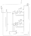
- FIG. 1 shows a schematic configuration of a wireless device 1 according to an embodiment (first embodiment) of the present invention.
- the wireless device 1 includes an antenna 20, a receiver 21, a microphone 22, an LCD 23, an LCD controller 24, and a wireless circuit 101.
- the radio circuit 101 includes an RFIC 120, a baseband IC (transmission system phase shifter control means) 121, a transmission system power amplifier (transmission system power amplifier) 140, a transmission system phase shifter (transmission system phase shifter) 141, and a coupler (measurement). Means) 142 and a galvanometer (measuring means) 143.
- a matching circuit for impedance matching of the antenna may be inserted between the antenna 20 and the phase shifter 141.
- the RF signal (transmission signal) output from the RFIC 120 is amplified by the transmission power amplifier 140 and transmitted by the antenna 20.
- the transmission system phase shifter 141 corrects the phase characteristic on the output side of the transmission system power amplifier 130, thereby correcting the phase relationship of the impedance between the transmission system power amplifier 130 side and the antenna 20 side.
- the coupler 142 measures the power of the RF signal amplified by the transmission power amplifier 140.
- the galvanometer 143 measures the current consumed in the transmission system power amplifier 140.
- the baseband IC 121 controls the amount of phase correction by the transmission phase shifter 141.
- phase correction refers to changing the phase without changing VSWR, and moves within a circle centered on the center of the chart (for example, 50 ⁇ ) on the Smith chart. Refers to the adjustment.
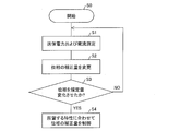
- FIG. 2 is a flowchart showing an example of an operation including phase correction in the present embodiment.
- the operation is not particularly limited, but may be any timing such as every predetermined time when the wireless device 1 is activated.
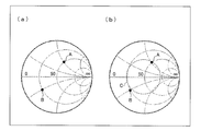
- detecting the start of communication by pressing the call start button detecting the change in the ratio of the power level of the traveling wave and backward wave that can be read by the bidirectional coupler, connecting to the power level of the traveling wave read from the bidirectional coupler and the power amplifier It is preferable to start when one of the detection of the change in power efficiency calculated from the current value read by the detected current detector, the proximity of the object to the communication device by the proximity sensor, or when a plurality of conditions are met . This is because there is a high possibility that the phase relationship has changed due to fluctuations in the antenna load (step S0). At this time, the impedance A on the transmission system power amplifier 140 side and the impedance B on the antenna side circuit are in a positional relationship as shown in FIG.
- step S1 the coupler 142 measures the transmission power amplified by the transmission system power amplifier 140, and the galvanometer 143 measures the current consumption in the transmission system power amplifier 140.
- the measurement result is sent to the baseband IC 121 via the RFIC 120, and the baseband IC 121 associates the information indicating the measurement result with a phase correction amount in the transmission phase shifter 150 in a memory or the like (not shown).
- the baseband IC 121 may store information indicating the transmission power and information indicating the current consumption, and indicate power efficiency (ratio of transmission power to power consumption) calculated from the information. Information may be stored.
- step S2 the baseband IC 121 changes the transmission system shift so that the phase correction amount in the transmission system phase shifter 141 changes in a certain direction (clockwise or counterclockwise on the Smith chart).
- the phaser 141 is controlled.
- the amount of change is not particularly limited and may be set as appropriate.
- the control method of the transmission phase shifter 141 by the baseband IC 121 is not limited to this.
- (i) parameters corresponding to each correction amount are stored in a memory (not shown) in advance.
- the parameter corresponding to the correction amount may be called, and the variable capacitance element, the variable induction element, the switch element, etc.
- the transmission phase shifter 141 may be controlled based on the called parameter, or (ii) depending on the correction amount
- the parameters may be calculated each time, and the variable capacitance elements, variable induction elements, switch elements, etc. in the transmission phase shifter 141 may be controlled based on the obtained parameters.
- step S3 it is determined whether or not the phase correction amount in the transmission phase shifter 141 has changed a prescribed phase change amount (for example, 360 °) from the start of the phase correction, and the change amount. If it is less than (the prescribed amount), the process returns to step S1, and if the prescribed amount is changed, the process moves to step S4.
- the characteristic transmission power, current consumption, or power efficiency
- step S4 the baseband IC 121 compares the characteristics (transmission power, current consumption, or power efficiency) associated with each correction amount stored so far, and sets a parameter corresponding to the correction amount that satisfies a desired condition.
- the transmission phase shifter 141 To control the transmission phase shifter 141. That is, when the purpose is to increase the transmission power, the transmission system phase shifter 141 is set so that the phase correction amount corresponds to the phase at which the maximum transmission power is measured among the transmission system power amplifiers 140. When the purpose is to reduce the current consumption, the transmission system shift is performed so that the phase correction amount corresponds to the phase that has the minimum current consumption measured by the transmission power amplifier 140.
- the phase shifter 141 may be controlled, and when the purpose is to increase the power efficiency, the transmission power amplifier 140 has a phase correction amount corresponding to the phase having the highest power efficiency among the measured power amplifiers 140.
- the transmission phase shifter 141 may be controlled. Further, any one of the measured characteristics (transmission power, current consumption, or power efficiency) above or below the threshold may be selected. If the phase relationship of the circuit impedance between the antenna side and the power amplifier side in the transmission phase shifter 141 is close to the complex conjugate relationship, the imaginary part is canceled and approaches the same resistance component, so the power amplifier side is larger than the antenna side. Electric power is supplied, and electric power can be improved. In addition, there is a device-specific load map in the transmission system power amplifier 140, and even if the impedance value is the same, the power, current characteristics, output power efficiency, etc. change depending on the phase. The characteristics can be improved successfully.
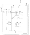
- FIG. 4 is a diagram illustrating a schematic configuration of the wireless device 2 according to an embodiment (second embodiment) of the present invention.
- the same members as those described in the first embodiment are denoted by the same member numbers, and description thereof is omitted.
- the receiver 21, the microphone 22, the LCD 23, and the LCD controller 24 are omitted.
- the wireless device 2 includes an antenna 20 and a wireless circuit 102.
- the radio circuit 102 includes an RFIC 120, a baseband IC 121, a transmission system power amplifier 140, a transmission system phase shifter 141, a coupler 142, a galvanometer 143, and a variable load (load fluctuation compensation means) 122.
- the variable load 122 is a load fluctuation compensation means for compensating for a load fluctuation of the antenna as described in Patent Documents 1 and 2. Note that a matching circuit for impedance matching of the antenna may be inserted between the antenna 20 and the variable load 122.
- FIG. 5 is a flowchart showing an example of an operation including phase correction in the present embodiment.
- step S10 the impedance A on the transmission system power amplifier 140 side and the impedance B of the antenna side circuit are in a positional relationship as shown in FIG. To do.
- the baseband IC 121 detects the change in the antenna load (step S11), and controls the variable load 122 so as to compensate for the variation in the antenna load (step S12).
- the impedance A on the transmission system power amplifier 140 side and the impedance B on the antenna side circuit have a relationship as shown in FIG.
- the load fluctuation amount may be calculated based on the current consumption, gain, and the like of the transmission power amplifier 140, and the load of the variable load 122 may be adjusted to compensate for the fluctuation.
- the baseband IC 121 can easily acquire the current consumption, gain, and the like of the transmission power amplifier 140 via the coupler 142 and the galvanometer 143.
- the baseband IC 121 may perform steps S11 and S12 based on experimentally obtained data stored in advance in a memory or the like (not shown). That is, it is possible to assume to some extent a scene that causes a load variation of the antenna. For example, when the wireless device 2 is a mobile phone terminal, a scene in which the mobile phone terminal is held by hand is assumed. At this time, since the way of holding the mobile phone terminal can be considered to be limited to several patterns, for each pattern, the amount of change in current consumption, gain, etc. of the transmission power amplifier 140 corresponding to the pattern, and The optimum adjustment amount of the variable load 122 can be experimentally obtained in advance.
- the baseband IC 121 detects the antenna load fluctuation (step S11) and the variable load 122 based on the data. Adjustment (step S12) can be performed.
- the baseband IC 121 performs the same processes as steps S1 to S4 of the first embodiment in step S13 after step S12. That is, the baseband IC 121 measures the transmission power and the current consumption in the transmission system power amplifier 140 via the coupler 143 and the galvanometer 150, and sets the phase correction amount in the transmission system phase shifter 141 to a specified amount (for example, 360 °). 6 (d), the characteristics (transmission power, current consumption, or power efficiency) at each position are changed while the impedance A on the transmission system power amplifier 140 side is changed around the circle C. Can be acquired. The baseband IC 121 controls the amount of phase correction in the transmission phase shifter 141 so that the most desired characteristic (transmission power, current consumption, or power efficiency) becomes high.
- the phase relationship of the circuit impedance between the antenna side and the power amplifier side in the transmission phase shifter 141 approaches the complex conjugate relationship
- the imaginary part is canceled and approaches the same resistance component. Therefore, a larger amount of power is supplied from the power amplifier side to the antenna side, and the power can be improved.
- there is a device-specific load map in the transmission system power amplifier 140 and even if the impedance value is the same, the power, current characteristics, output power efficiency, etc. change depending on the phase. The characteristics can be improved successfully.
- the baseband IC 121 may determine the phase correction amount in the transmission phase shifter 141 based on the optimum adjustment amount of the variable load 122 obtained in step S12 in step S13. .
- the phase correction amount in the transmission phase shifter 141 can be determined with a simple configuration. This is because a situation in which the load of the antenna fluctuates, that is, a change in the phase relationship between the impedance of the antenna side circuit and the impedance of the power amplifier side circuit, can be assumed to some extent, Since it is possible to assume the position of the antenna-side impedance after compensation from the compensation amount, it is possible to associate the compensation amount of the load fluctuation with the phase correction amount by the transmission phase shifter in advance. Is possible.
- the phase shifter control unit (baseband IC 121) controls the phase correction amount in the transmission system phase shifter so as to correspond to the load variation compensation amount by the load variation compensation unit, thereby transmitting the transmission system shift.
- the amount of phase correction by the phase shifter can be controlled.
- the phase shifter control means can determine the correction amount more easily than when the correction amount is determined by monitoring the current consumption of the power amplifier, the transmission power of the transmission signal, and the like.
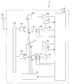
- FIG. 7 is a diagram illustrating a schematic configuration of a wireless device 3 according to an embodiment (third embodiment) of the present invention.
- the same members as those described in the first and second embodiments are denoted by the same member numbers, and description thereof is omitted.
- the receiver 21, the microphone 22, the LCD 23, and the LCD controller 24 are omitted.
- the wireless device 3 includes an antenna 20 and a wireless circuit 103.
- the radio circuit 103 includes an RFIC 120, a baseband IC 121, a transmission system power amplifier 140, a coupler 142, a variable load (load fluctuation compensation means) 122, a duplexer (antenna sharing device) 123, a reception system power amplifier (reception system power amplifier) 160, In addition, a reception system phase shifter 161 is provided.
- the duplexer 123 is a member for sharing the antenna 20 between the transmission system and the reception system.
- the reception signal received by the antenna 20 passes through a transmission path whose phase characteristics (the phase relationship of impedance between the reception system power amplifier 160 side and the antenna 20 side) are corrected by the reception system phase shifter 161, and the reception system power amplifier 160. Is amplified and sent to the RFIC 120. Note that a matching circuit for impedance matching of the antenna may be inserted between the antenna 20 and the variable load 122.
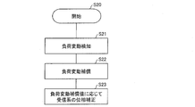
- FIG. 8 is a flowchart showing an example of an operation including phase correction in the present embodiment.
- the baseband IC 121 first detects a change in the antenna load of the antenna 20 (step S21), and controls the variable load 122 so as to compensate for the variation in the antenna load (step S21). S22). Steps S21 and S22 can be performed in the same manner as steps S11 and S12 of the second embodiment.
- the baseband IC 121 controls the phase correction amount by the reception phase shifter 161 in accordance with the compensation amount (load fluctuation compensation value) of the variable load 122 in step S22.
- the correspondence relationship between the load fluctuation compensation value and the correction amount is stored in advance in a memory or the like (not shown) as a table, and the baseband IC 121 calls the correspondence relationship, and the reception system phase shifter 161
- the reception phase shifter 161 is controlled so that the phase correction amount becomes a correction amount corresponding to the load fluctuation compensation value in step S22.
- the characteristic of the reception system power amplifier 160 can be improved. This is due to the following reasons.
- phase shifter control means controls the phase correction amount by the phase shifter by controlling the phase correction amount in the phase shifter so as to correspond to the load fluctuation compensation amount by the load fluctuation compensation means. can do.
- the correction amount of the reception system phase shifter 161 (the value that improves the characteristics of the reception system power amplifier 160) in the load fluctuation compensation value of the variable load 122 for each pattern of how to hold the mobile phone terminal is set in advance. Find and relate experimentally.
- the baseband IC 121 detects the variable load based on the data when the antenna load fluctuation is detected (step S21).
- the control (step S23) of the reception system phase shifter 161 can be performed.
- the correspondence relationship between the load fluctuation compensation value and the phase correction amount of the transmission phase shifter 141 is stored in advance in a memory or the like (not shown) as a table.
- the phase correction amount corresponding to the load fluctuation compensation value is not necessarily limited to one, and a plurality of correction amounts may correspond to one load fluctuation compensation value.
- the baseband IC 121 may control the phase shifter by selecting any one of a plurality of phase correction amounts corresponding to the load fluctuation compensation value, or may try each correction amount to determine characteristics such as current consumption. The correction amount with the best characteristics may be selected.
- phase relationship of the circuit impedance between the antenna side and the power amplifier side in the reception system phase shifter 161 approaches the complex conjugate relationship by moving the reception system phase shifter 161 as described above, the imaginary part is canceled. Since the same resistance component is approached, a larger amount of power is supplied from the antenna side to the power amplifier side, thereby improving the power.
- there is a device-specific load map in the receiving system power amplifier 160 and even if the impedance value is the same, the power, current characteristics, output power efficiency, etc. change depending on the phase. The characteristics can be improved successfully.
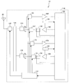
- FIG. 9 is a diagram illustrating a schematic configuration of a wireless device 4 according to an embodiment (fourth embodiment) of the present invention.
- the same members as those described in the first to third embodiments are denoted by the same member numbers, and description thereof is omitted.
- the receiver 21, the microphone 22, the LCD 23, and the LCD controller 24 are omitted.
- the wireless device 4 includes an antenna 20 and a wireless circuit 104.
- the radio circuit 104 includes an RFIC 120, a baseband IC 121, a transmission system power amplifier 140, a transmission system phase shifter 141, a coupler 142, a current detector 143, a duplexer 123, a reception system power amplifier 160, and a reception system phase shifter 161. I have.
- the wireless device 4 includes both the combination of the transmission system power amplifier 140 and the transmission system phase shifter 141 and the combination of the reception system power amplifier 160 and the reception system phase shifter 161. Yes.
- a matching circuit for impedance matching of the antenna may be inserted between the antenna 20 and the duplexer 123.
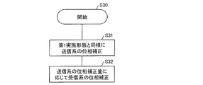
- FIG. 10 is a flowchart showing an example of an operation including phase correction in the present embodiment.
- the baseband IC 121 controls the correction amount of the phase of the transmission phase shifter 141 as in steps S1 to S4 of the first embodiment (step S31).
- the baseband IC 121 controls the correction amount of the phase by the reception phase shifter 161 according to the correction amount of the phase of the transmission phase shifter 141 in step S31.
- the correspondence between the phase correction amount of the transmission phase shifter 141 and the phase correction amount of the reception phase shifter 161 is stored in advance in a memory or the like (not shown) as a table, and the baseband IC 121 The corresponding relationship is called, and the reception phase shifter 161 is set so that the phase correction amount by the reception phase shifter 161 becomes a correction amount corresponding to the phase correction amount of the transmission phase shifter 141 in step S31. Control. Thereby, the characteristic of the reception system power amplifier 160 can be improved. This is due to the following reasons.
- the phase shifter control means can control the phase correction amount by the receiving phase shifter to improve the characteristics. This is because the correction amount of the reception phase shifter can be determined by associating the correction amount of the phase by the reception phase shifter in advance with the correction amount of the phase in the transmission phase shifter. Therefore, the phase shifter control means controls the phase correction amount in the reception system phase shifter to control the phase correction amount in the reception system phase shifter so as to correspond to the phase correction amount in the transmission system phase shifter. The characteristic can be improved by controlling the correction amount.
- the correction amount of the reception system phase shifter 161 (the value that improves the characteristics of the reception system power amplifier 160) in the compensation value of the transmission system phase shifter is experimentally obtained in advance and correlated. Then, by storing the experimentally obtained data in a memory or the like (not shown) in advance, the baseband IC 121 can change based on the data when the antenna load fluctuation is detected (step S21). In addition to the adjustment of the load 122 (step S22), the control of the reception system phase shifter 161 (step S23) can be performed.
- the phase relationship of the circuit impedance between the antenna side and the power amplifier side in the transmission system phase shifter 141 and the reception system phase shifter 161 is When approaching the complex conjugate relationship, the imaginary part is canceled and approaches the same resistance component, so that a larger amount of power is supplied from the power amplifier side to the antenna side and from the antenna side to the power amplifier side. It becomes possible.
- the transmission power amplifier 140 and the reception power amplifier 160 have device-specific load maps. Even if the impedance value is the same, the power, current characteristics, output power efficiency, etc. vary depending on the phase. By changing the desired characteristics can be improved successfully. [Fifth Embodiment] FIG.
- FIG. 11 is a diagram illustrating a schematic configuration of a wireless device 5 according to an embodiment (fifth embodiment) of the present invention.
- the same members as those described in the first to fourth embodiments are denoted by the same member numbers, and description thereof is omitted.
- the receiver 21, the microphone 22, the LCD 23, and the LCD controller 24 are omitted.
- the wireless device 5 includes an antenna 20 and a wireless circuit 105.
- the radio circuit 105 includes an RFIC 120, a baseband IC 121, a variable load 122, a transmission system power amplifier 140, a transmission system phase shifter 141, a coupler 142, a current detector 143, a duplexer 123, a reception system power amplifier 160, and a reception system shift.
- a phaser 161 is provided. Note that a matching circuit for impedance matching of the antenna may be inserted between the antenna 20 and the variable load 122.
- FIG. 12 is a flowchart showing an example of an operation including phase correction in the present embodiment.
- the baseband IC 121 first detects a change in the antenna load of the antenna 20 (step S41), and controls the variable load 122 so as to compensate for the variation in the antenna load (step S41).
- Steps S41 and S42 can be performed in the same manner as steps S11 and S12 of the second embodiment.
- the baseband IC 121 controls the correction amount of the phase of the transmission phase shifter 141 in the same manner as steps S1 to S4 of the first embodiment (step S43). Subsequently, in step S44, the baseband IC 121 controls the phase correction amount by the reception system phase shifter 161 according to the phase correction amount of the transmission system phase shifter 141 in step S43.
- step S44 the reception phase shifter 161 may be controlled so that the correction amount corresponds to the load fluctuation compensation value in step S42.
- the phase relationship of the circuit impedance between the antenna side and the power amplifier side in the transmission system phase shifter 141 and the reception system phase shifter 161 is When approaching the complex conjugate relationship, the imaginary part is canceled and approaches the same resistance component, so that more power is supplied from the power amplifier side to the antenna side, and from the antenna side to the power amplifier side. It becomes possible.
- the transmission power amplifier 140 and the reception power amplifier 160 have device-specific load maps. Even if the impedance value is the same, the power, current characteristics, output power efficiency, etc. vary depending on the phase. By changing the desired characteristics can be improved successfully.
- FIG. 13 is a diagram illustrating a schematic configuration of a wireless device 6 according to an embodiment (sixth embodiment) of the present invention.
- This embodiment has a configuration in which a plurality of transmission systems in the first embodiment are provided, and has a configuration in which a transmission system connected to the antenna 20 among the plurality of transmission systems is switched by a switch 125.
- the same members as those described in the first embodiment are denoted by the same member numbers, and description thereof is omitted.
- the receiver 21, the microphone 22, the LCD 23, and the LCD controller 24 are omitted.
- Each transmission system has a different frequency band.
- the wireless device 6 includes an antenna 20 and a wireless circuit 106.
- the radio circuit 106 includes an RFIC 120, a baseband IC 121, transmission power amplifiers 140 and 150, transmission phase shifters 141 and 151, couplers 142 and 152, galvanometers 143 and 153, and a switch 125. Note that a matching circuit for impedance matching of the antenna may be inserted between the antenna 20 and the switch 125.
- the same effect as in the first embodiment can be obtained. That is, by moving the transmission system phase shifters 141 and 151, if the phase relationship of the circuit impedance between the antenna side and the power amplifier side in the transmission system phase shifters 141 and 151 approaches a complex conjugate relationship, the imaginary part is canceled. Thus, since the same resistance component is approached, a larger amount of power is supplied from the power amplifier side to the antenna side, thereby improving the power.
- the transmission power amplifiers 140 and 150 have device-specific load maps, and even with the same impedance value, the power, current characteristics, output power efficiency, etc. change depending on the phase. Desired characteristics can be improved successfully.
- FIG. 14 is a diagram illustrating a schematic configuration of a wireless device 7 according to an embodiment (seventh embodiment) of the present invention.
- This embodiment has a configuration in which a plurality of transmission systems in the second embodiment are provided, and has a configuration in which a transmission system connected to the antenna 20 is switched by the switch 125 among the plurality of transmission systems.
- the same members as those described in the second embodiment are denoted by the same member numbers, and description thereof is omitted.
- the receiver 21, the microphone 22, the LCD 23, and the LCD controller 24 are omitted.
- the wireless device 7 includes an antenna 20 and a wireless circuit 107.
- the radio circuit 107 includes an RFIC 120, a baseband IC 121, transmission power amplifiers 140 and 150, transmission phase shifters 141 and 151, couplers 142 and 152, galvanometers 143 and 153, a variable load 122, and a switch 125.
- a matching circuit for impedance matching of the antenna may be inserted between the antenna 20 and the variable load 122.
- the same effect as in the second embodiment can be obtained. That is, by moving the transmission system phase shifters 141 and 151, if the phase relationship of the circuit impedance between the antenna side and the power amplifier side in the transmission system phase shifters 141 and 151 approaches a complex conjugate relationship, the imaginary part is canceled. Thus, since the same resistance component is approached, a larger amount of power is supplied from the power amplifier side to the antenna side, thereby improving the power.
- the transmission power amplifiers 140 and 150 have device-specific load maps, and even with the same impedance value, the power, current characteristics, output power efficiency, etc. change depending on the phase. Desired characteristics can be improved successfully.
- FIG. 15 is a diagram illustrating a schematic configuration of a wireless device 8 according to an embodiment (eighth embodiment) of the present invention.
- This embodiment has a configuration in which a plurality of transmission / reception systems in the third embodiment are provided, and has a configuration in which a transmission / reception system connected to the antenna 20 is switched by a switch 125 among the plurality of transmission / reception systems.
- the same members as those described in the third embodiment are denoted by the same member numbers, and description thereof is omitted.
- the receiver 21, the microphone 22, the LCD 23, and the LCD controller 24 are omitted.
- Each transmission / reception system has different frequency bands.
- the radio device 8 includes an antenna 20 and a radio circuit 108.
- Radio circuit 108 includes RFIC 120, baseband IC 121, transmission power amplifiers 140 and 150, couplers 142 and 152, variable load 122, duplexers 123 and 124, reception power amplifiers 160 and 170, reception phase shifters 161 and 171,
- a switch 125 is provided. Note that a matching circuit for impedance matching of the antenna may be inserted between the antenna 20 and the variable load 122.
- the same effect as in the third embodiment can be obtained. That is, by moving the reception phase shifters 161 and 171 as described above, if the phase relationship of the circuit impedance between the antenna side and the power amplifier side in the reception phase shifters 161 and 171 is close to the complex conjugate relationship, Since the imaginary part is canceled and approaches the same resistance component, a larger amount of power is supplied from the antenna side to the power amplifier side, and power improvement is possible. In addition, there is a device-specific load map in the receiving system power amplifiers 160 and 170. Even if the impedance value is the same, the power, current characteristics, output power efficiency, etc. change depending on the phase. Desired characteristics can be improved successfully.
- FIG. 16 is a diagram illustrating a schematic configuration of a wireless device 9 according to an embodiment (9th embodiment) of the present invention.
- This embodiment has a configuration provided with a plurality of transmission / reception systems in the fourth embodiment, and has a configuration in which a transmission / reception system connected to the antenna 20 is switched by a switch 125 among the plurality of transmission / reception systems.
- the same members as those described in the fourth embodiment are denoted by the same member numbers, and description thereof is omitted.
- the receiver 21, the microphone 22, the LCD 23, and the LCD controller 24 are omitted.
- Each transmission / reception system has different frequency bands.
- the wireless device 9 includes an antenna 20 and a wireless circuit 109.
- Radio circuit 109 includes RFIC 120, baseband IC 121, transmission system power amplifiers 140 and 150, transmission system phase shifters 141 and 151, couplers 142 and 152, galvanometers 143 and 153, duplexers 123 and 124, and reception system power amplifier 160. 170, receiving phase shifters 161 and 171, and a switch 125. Note that a matching circuit for impedance matching of the antenna may be inserted between the antenna 20 and the switch 125.
- the same effects as in the fourth embodiment can be obtained. That is, by moving the transmission phase shifters 141 and 151 and the reception phase shifters 161 and 171 as described above, the antenna side and power in the transmission phase shifters 141 and 151 and the reception phase shifters 161 and 171 are moved.
- the phase relationship of the circuit impedance with the amplifier side approaches the complex conjugate relationship, the imaginary part is canceled and approaches the same resistance component, so that a larger amount of power is generated from the power amplifier side to the antenna side and from the antenna side to the power amplifier side. As a result, the power can be improved.
- device-specific load maps exist in the transmission power amplifiers 140 and 150 and the reception power amplifiers 160 and 170, and the power, current characteristics, output power efficiency, and the like change depending on the phase even with the same impedance value. Desired characteristics can be successfully improved by changing the phase by the phase shifter.
- FIG. 17 is a diagram illustrating a schematic configuration of a wireless device 10 according to an embodiment (tenth embodiment) of the present invention.
- the present embodiment has a configuration in which a plurality of transmission / reception systems in the fifth embodiment are provided, and has a configuration in which a transmission / reception system connected to the antenna 20 is switched by a switch 125 among the plurality of transmission / reception systems.
- the same members as those described in the fifth embodiment are denoted by the same member numbers, and description thereof is omitted.
- the receiver 21, the microphone 22, the LCD 23, and the LCD controller 24 are omitted.
- Each transmission / reception system has different frequency bands.
- the wireless device 10 includes an antenna 20 and a wireless circuit 110.
- Radio circuit 110 includes RFIC 120, baseband IC 121, variable load 122, transmission system power amplifiers 140 and 150, transmission system phase shifters 141 and 151, couplers 142 and 152, galvanometers 143 and 153, duplexers 123 and 124, and reception.
- a matching circuit for impedance matching of the antenna may be inserted between the antenna 20 and the variable load 122.
- the same effect as in the fifth embodiment can be obtained. That is, by moving the transmission phase shifters 141 and 151 and the reception phase shifters 161 and 171 as described above, the antenna side and power in the transmission phase shifters 141 and 151 and the reception phase shifters 161 and 171 are moved.
- the phase relationship of the circuit impedance with the amplifier side approaches the complex conjugate relationship, the imaginary part is canceled and approaches the same resistance component, so that a larger amount of power is generated from the power amplifier side to the antenna side and from the antenna side to the power amplifier side. As a result, the power can be improved.
- device-specific load maps exist in the transmission power amplifiers 140 and 150 and the reception power amplifiers 160 and 170, and the power, current characteristics, output power efficiency, and the like change depending on the phase even with the same impedance value. Desired characteristics can be successfully improved by changing the phase by the phase shifter.
- the baseband IC (phase shifter control means) 120 described above may be configured by hardware logic, or may be realized by software using a CPU as follows.
- the wireless device 1 includes a CPU (central processing unit) that executes instructions of a control program that implements each function, a ROM (read only memory) that stores the program, a RAM (random access memory) that expands the program, A storage device (recording medium) such as a memory for storing the program and various data is provided.
- the object of the present invention is to record the program code (execution format program, intermediate code program, source program) of the control program (authentication program) of the wireless device 1 which is software that realizes the above-described functions in a computer-readable manner. This can also be achieved by supplying a recording medium to the portable communication device 1 and reading and executing the program code recorded on the recording medium by the computer (or CPU or MPU).
- Examples of the recording medium include tapes such as magnetic tapes and cassette tapes, magnetic disks such as floppy (registered trademark) disks / hard disks, and disks including optical disks such as CD-ROM / MO / MD / DVD / CD-R.
- Card system such as IC card, IC card (including memory card) / optical card, or semiconductor memory system such as mask ROM / EPROM / EEPROM / flash ROM.
- the wireless device 1 may be configured to be connectable to a communication network, and the program code may be supplied via the communication network.
- the communication network is not particularly limited.
- the Internet intranet, extranet, LAN, ISDN, VAN, CATV communication network, virtual private network, telephone line network, mobile communication network, satellite communication. A net or the like is available.
- the transmission medium constituting the communication network is not particularly limited.
- infrared rays such as IrDA and remote control, Bluetooth ( (Registered trademark), 802.11 wireless, HDR (high data rate), mobile phone network, satellite line, terrestrial digital network, and the like can also be used.
- the present invention can also be realized in the form of a computer data signal embedded in a carrier wave in which the program code is embodied by electronic transmission.
- the wireless circuit according to the present invention is not necessarily limited to the structure in which each member is disposed on the substrate, and may have a structure in which all members are configured in one element.
- the present invention is not limited to the above-described embodiments, and various modifications are possible within the scope shown in the claims, and embodiments obtained by appropriately combining technical means disclosed in different embodiments. Is also included in the technical scope of the present invention.
- a radio circuit according to the present invention includes a phase shifter that is connected between an antenna and a power amplifier and corrects the impedance phase relationship between the antenna side and the power amplifier side in order to solve the above problem. It is characterized by having.
- the phase shifter is inserted between the antenna and the power amplifier, and the phase relationship between the impedance of the antenna side circuit and the impedance of the power amplifier side circuit is corrected based on the phase shifter. Therefore, good characteristics of the power amplifier can be obtained.
- correcting the phase relationship between the antenna side and the power amplifier side means a phase between the impedance of the antenna side circuit and the impedance of the power amplifier side circuit so as to improve the above characteristics. It means changing the relationship by turning the phase of the phase shifter.
- the radio circuit according to the present invention it is preferable that no isolator be inserted between the antenna and the power amplifier.
- a wireless circuit that does not include an isolator has low power loss and can reduce the area occupied by the circuit, but has a problem of unstable power amplifier characteristics. According to the above configuration, the phase relationship between the impedance of the antenna side circuit and the impedance of the power amplifier side circuit from the phase shifter can be corrected, so that the above problem can be reduced and good characteristics of the power amplifier can be obtained. be able to.
- the power amplifier is a transmission system power amplifier that amplifies a transmission signal transmitted from the antenna, and the phase shifter is disposed between the transmission system power amplifier and the antenna.
- a connected transmission phase shifter may be used.
- the wireless circuit preferably includes a phase shifter control means for controlling the amount of phase correction by the transmission phase shifter.
- the phase shifter control means controls the amount of correction of the phase by the transmission phase shifter, so that the phase relationship between the impedance of the antenna side circuit and the impedance of the power amplifier side circuit can be easily set. Can be adjusted.
- characteristics such as current consumption and transmission power of the power amplifier vary depending on the phase relationship between the impedance of the antenna side circuit and the impedance of the power amplifier side circuit. Therefore, according to the above configuration, the transmission power of the transmission signal, the current consumption of the transmission power amplifier, and the power efficiency that is the ratio of the transmission power to the current consumption are improved. Can be made.
- the radio circuit includes a measurement unit that measures at least one of a current consumption of the transmission power amplifier and a transmission power of the transmission signal, and the phase shifter control unit is configured to perform measurement based on a measurement result of the measurement unit. It is preferable to control the correction amount of the phase by the transmission phase shifter.
- the phase shifter control means can perform the above control more easily.
- the phase shifter control means measures at least one of the consumption current and the transmission power via the measurement means while changing the correction amount of the phase by the transmission phase shifter. Based on the measurement result, the transmission power, the current consumption, and at least one characteristic selected from the group consisting of power efficiency that is a ratio of the transmission power to the current consumption is improved. It is preferable to control the correction amount of the phase by the system phase shifter.
- the phase shifter control means can successfully find the correction amount of the phase that can improve the desired characteristics, so that it is possible to easily obtain good characteristics of the transmission power amplifier. Can do.
- a duplexer that demultiplexes a signal in a transmission / reception band is inserted between the transmission phase shifter and the antenna or the matching circuit, and a reception system that amplifies a reception signal received by the antenna A power amplifier; and a receiving phase shifter connected between the receiving power amplifier and the duplexer for correcting the phase of the received signal;
- the phase shifter control means may control the phase correction amount in the reception system phase shifter so as to correspond to the phase correction amount in the transmission system phase shifter.
- the phase shifter control means can control the phase correction amount by the receiving phase shifter to improve the characteristics. This is because the correction amount of the reception phase shifter can be determined by associating the correction amount of the phase by the reception phase shifter in advance with the correction amount of the phase in the transmission phase shifter. Therefore, the phase shifter control means controls the phase correction amount in the reception system phase shifter to control the phase correction amount in the reception system phase shifter so as to correspond to the phase correction amount in the transmission system phase shifter. The characteristic can be improved by controlling the correction amount.
- the radio circuit may further include a load fluctuation compensation unit that is connected between the phase shifter and the antenna and compensates for a load fluctuation of the antenna.
- the radio circuit is further connected to the transmission phase shifter and the antenna, and further includes load fluctuation compensation means for compensating for load fluctuation of the antenna, and the phase shifter control means includes the load fluctuation compensation means.
- the amount of correction of the phase in the transmission phase shifter may be controlled so as to correspond to the amount of compensation for the load fluctuation by the means.
- a duplexer for demultiplexing a signal in the transmission / reception band is inserted between the transmission phase shifter and the load fluctuation compensation means, and reception system power for amplifying the reception signal received by the antenna An amplifier, and a receiving phase shifter connected between the receiving power amplifier and the duplexer for correcting the phase of the received signal, and the phase shifter control means includes the load fluctuation compensation
- the amount of correction of the phase in the reception phase shifter may be controlled so as to correspond to the amount of compensation for the load fluctuation by the means.
- the phase shifter control means can control the phase correction amount by the transmission system phase shifter or the transmission / reception system phase shifter to an appropriate value. This is because a situation in which the load of the antenna fluctuates, that is, a change in the phase relationship between the impedance of the antenna side circuit and the impedance of the power amplifier side circuit, can be assumed to some extent, Since it is also possible to assume the position of the antenna-side impedance after compensation from the compensation amount, the phase correction amount by the transmission system phase shifter or the transmission / reception system phase shifter with respect to the load variation compensation amount It is possible to associate them.
- the phase shifter control unit controls the phase correction amount in the transmission system phase shifter or the transmission / reception system phase shifter so as to correspond to the load variation compensation amount by the load variation compensation unit, thereby transmitting the transmission system.
- the amount of phase correction by the phase shifter or the transmission / reception system phase shifter can be controlled.
- the phase shifter control means can determine the correction amount more easily than when the correction amount is determined by monitoring the current consumption of the power amplifier, the transmission power of the transmission signal, and the like.
- Load variation compensation means connected between the duplexer and the antenna and compensating for load fluctuation of the antenna is further provided, and the phase shifter control means compensates for the load fluctuation by the load fluctuation compensation means.
- the phase correction amount in the reception phase shifter may be controlled so as to correspond to the amount.
- the phase shifter control means can determine the phase correction amount in the transmission phase shifter and the phase correction amount in the reception phase shifter in parallel.
- the power amplifier is a reception system power amplifier that amplifies a reception signal received by the antenna, and the phase shifter is connected between the reception system power amplifier and the antenna. It may be a receiving phase shifter.
- the phase shifter control means can control the correction amount of the phase by a receiving system phase shifter to an appropriate value. Because it is possible to assume to some extent changes in the phase relationship between the impedance of the antenna side circuit and the impedance of the power amplifier side circuit, such as when the antenna load fluctuates. This is because it is possible to improve by storing several types of phase correction amounts in advance and selecting from among them. Therefore, the phase shifter control means can control the amount of phase correction in the reception phase shifter.
- the radio circuit connected between the receiving phase shifter and the antenna, and corresponding to the load fluctuation compensation means for compensating for the load fluctuation of the antenna, and the compensation amount of the load fluctuation by the load fluctuation compensation means
- a phase shifter control means for controlling the amount of correction of the phase in the reception system phase shifter.
- the phase shifter control means can control the correction amount of the phase by the reception system phase shifter to an appropriate value. This is because a situation in which the load of the antenna fluctuates, that is, a change in the phase relationship between the impedance of the antenna side circuit and the impedance of the power amplifier side circuit, can be assumed to some extent, Since it is also possible to assume the position of the antenna-side impedance after compensation from the compensation amount, it is possible to associate the compensation amount of the load variation with the phase correction amount by the receiving phase shifter in advance. Is possible. Therefore, the phase shifter control means controls the phase correction amount in the reception system phase shifter so as to correspond to the load fluctuation compensation amount by the load fluctuation compensation means, so that the phase shift by the reception system phase shifter is controlled. The correction amount can be controlled.
- each reception system may include a combination of the above reception system power amplifier and the above reception system phase shifter when the antenna supports a plurality of reception bands / transmission bands.
- Each transmission system may include a combination of the transmission system power amplifier and the transmission system phase shifter.
- the radio apparatus according to the present invention is characterized by including the radio circuit according to the present invention.
- the radio apparatus control method includes: a current consumption of the transmission system power amplifier while changing the amount of correction of the phase by the transmission system phase shifter; and the transmission amplified by the transmission system power amplifier.
- a measurement step of measuring at least one of the transmission power of the signal, and based on a measurement result of the measurement step, the transmission power, the current consumption, and a power efficiency that is a ratio of the transmission power to the current consumption And a first control step of controlling a correction amount of the phase by the transmission phase shifter so as to improve at least one characteristic selected from the group.
- the radio apparatus control method includes: a current consumption of the transmission system power amplifier while changing the amount of correction of the phase by the transmission system phase shifter; and the transmission amplified by the transmission system power amplifier.
- a second control step of controlling the correction amount of the phase in the reception phase shifter so as to correspond to the correction amount of the phase may be included.
- the good characteristics of the transmission power amplifier in addition to the good characteristics of the transmission power amplifier, the good characteristics of the reception power amplifier that amplifies the received signal received by the antenna can be obtained.
- a control method of a radio apparatus includes an antenna, a reception system power amplifier that amplifies a reception signal received by the antenna, the reception system power amplifier, and the antenna,
- a control method for a radio apparatus comprising: a receiving phase shifter that corrects a phase; and a load fluctuation compensating unit that is connected between the receiving phase shifter and the antenna and compensates for a load fluctuation of the antenna.
- the load fluctuation compensation means compensates for the load fluctuation of the antenna, and the phase of the phase in the reception phase shifter so as to correspond to the compensation amount of the load fluctuation by the load fluctuation compensation means. And a control step of controlling the correction amount.
- a program for operating a computer included in the wireless device the program for causing the computer to execute as the phase shifter control means, and a computer-readable recording medium storing the program are also included in the present invention. Included in the technical scope.
- the present invention can be used in the general field of manufacturing wireless circuits and wireless devices.
- Radio equipment 20 Antenna 101 to 110 Radio circuit 120 RFIC 121 Baseband IC (phase shifter control means) 122 Variable load (load fluctuation compensation means) 123, 124 Duplexer 125 Switch 140, 150 Transmission system power amplifier (Transmission system power amplifier) 141, 151 Transmission system phase shifter (transmission system phase shifter) 142, 152 coupler (measuring means) 143, 153 Current detector (measuring means) 160, 170 Receiving power amplifier (Receiving power amplifier) 161, 171 Reception system phase shifter (Reception system phase shifter)
Landscapes
- Engineering & Computer Science (AREA)
- Computer Networks & Wireless Communication (AREA)
- Signal Processing (AREA)
- Transmitters (AREA)
- Amplifiers (AREA)
- Transceivers (AREA)
Abstract
無線回路(101)は、アンテナ(20)とパワーアンプ(140)との間に接続され、アンテナ側と電力増幅器側の位相関係を補正する移相器(141)を備えている。
Description
本発明は、無線回路、無線装置、および、無線装置の制御方法に関する。
無線装置を手で持ったとき、または、金属のようなアンテナ特性に影響を及ぼす物体を無線装置を近づけたときに、アンテナの負荷が変動し、無線装置に好ましくない影響を与える場合がある。
特に、アイソレータを備えていない無線装置では、アンテナのインピーダンス変動によりVSWR特性が劣化するだけでなく、前記変動が電力増幅器(パワーアンプ)につたわり、アンテナと電力増幅器との位相関係が変動して、電力増幅器の電流、出力電力、電力効率のような特性が劣化する場合がある。
公知技術として、アンテナのインピーダンス変動を検知して、VSWR特性を補償する技術が知られている(特許文献1、2)。すなわち、(i)パワーアンプとアンテナとの間に可変負荷を配置し、(ii)パワーアンプの電流値、利得の変化等に基づいてアンテナのインピーダンス変動を検知し、(iii)変動を補償するように、上記可変負荷を制御することにより、VSWR特性の劣化を抑制する。
無線装置を把持したとき、または、金属のようなアンテナ特性に影響のある物体を無線装置に近づけたときに、アンテナのインピーダンスが変動する。前記特許文献の技術では、前記変動に対してアンテナのVSWRを補正しているが、アンテナと増幅器のインピーダンスの位相関係がずれるという問題がある。
本発明は、上記課題に鑑みてなされたものであり、アンテナのインピーダンスが変動したときに、アンテナと増幅器のインピーダンスの位相関係のずれを解消するための技術を提供することを主たる目的とする。
本発明に係る無線回路は、上記課題を解決するために、アンテナと電力増幅器との間に接続され、該アンテナ側と該電力増幅器側とのインピーダンスの位相関係を補正する移相器を備えていることを特徴としている。
無線回路のアンテナと電力増幅器との間では、リターンロスが同じ値をとる場合でも、電力増幅器側とアンテナ側との位相関係により、電力増幅器の消費電流、出力電力、電力効率といった特性が変化する。上記の構成によれば、アンテナと電力増幅器との間に移相器が挿入されており、該移相器を基準としてアンテナ側回路のインピーダンスと、電力増幅器側回路のインピーダンスとの位相関係を補正することができるため、電力増幅器の良好な特性を得ることができる。
なお、本明細書において、「アンテナ側と電力増幅器側との位相関係を補正する」とは、上記特性を改善するようにアンテナ側回路のインピーダンスと、電力増幅器側回路のインピーダンスとの間の位相関係を、移相器の位相を回して変えることを意味する。
また、本明細書において、「移相器がアンテナと電力増幅器との間に接続されている」とは、アンテナと電力増幅器が移相器を介して接続されている状態を意味し、アンテナと移相器との間、および、移相器と電力増幅器との間に、他の素子または回路が挿入されることを妨げない。例えば、アンテナと移相器との間に、アンテナのインピーダンス整合のための整合回路が挿入されていてもよい。
本発明により、パワーアンプとアンテナの位相関係の補正を行い電力、または電流、または電力効率の特性の少なくとも1つを改善する。
〔第1実施形態〕
本発明に係る無線装置および無線回路のいくつかの実施形態について図面を参照して説明すれば以下のとおりである。なお、各実施形態に係る無線装置および無線回路は、通話のための無線通信を基地局との間で行なう携帯電話端末および当該携帯電話端末が備える無線回路として実現されている。以下では、各実施形態に係る無線装置を端的に携帯電話端末と称する。
本発明に係る無線装置および無線回路のいくつかの実施形態について図面を参照して説明すれば以下のとおりである。なお、各実施形態に係る無線装置および無線回路は、通話のための無線通信を基地局との間で行なう携帯電話端末および当該携帯電話端末が備える無線回路として実現されている。以下では、各実施形態に係る無線装置を端的に携帯電話端末と称する。
ただし、本発明は、通話のための無線通信を基地局との間で行なう携帯電話端末に限らず、何らかの信号が重畳された搬送波を、アンテナを用いて受信および/または送信する無線装置一般および当該無線装置が備える無線回路に適用することができる。例えば、本発明の無線装置および無線回路は、無線で放送を受信する放送受信装置および当該放送受信装置が備える無線回路であってもよい。
図1に、本発明の一実施形態(第1実施形態)に係る無線装置1の概略構成を示す。図1に示すように、無線装置1は、アンテナ20、レシーバ21、マイク22、LCD23、LCDコントローラ24および無線回路101を備えている。無線回路101は、RFIC120、ベースバンドIC(送信系移相器制御手段)121、送信系パワーアンプ(送信系電力増幅器)140、送信系移相器(送信系移相器)141、カプラ(測定手段)142、および、検流器(測定手段)143を備えている。なお、アンテナ20と移相器141との間に、アンテナのインピーダンス整合のための整合回路が挿入されていてもよい。
RFIC120から出力されたRF信号(送信信号)は、送信系パワーアンプ140によって増幅され、アンテナ20によって送信される。
送信系移相器141は、送信系パワーアンプ130の出力側の位相特性を補正し、これにより、信系パワーアンプ130側とアンテナ20側とのインピーダンスの位相関係を補正する。カプラ142は、送信系パワーアンプ140によって増幅されたRF信号の電力を測定する。
また、検流器143は、送信系パワーアンプ140において消費される電流を測定する。そして、ベースバンドIC121は、送信系移相器141による位相の補正量を制御する。
なお、本明細書において、位相の補正とは、VSWRを変化させずに、位相を変化させることを指し、スミスチャート上において、チャートの中心(例えば、50Ω)を中心とした円内を移動するように調整することを指す。
図2は、本実施形態における位相補正を含む動作の一例を示すフローチャートである。当該動作は、特に限定されないが、無線装置1の起動時、所定の時間毎などの任意のタイミングでもかまわない。
例えば、通話開始ボタンの押下などによる通信の開始の検知、双方向カプラにより読み取れる進行波と後退波の電力レベルの比の変化の検知、双方向カプラから読み取る進行波の電力レベルと電力増幅器に接続された検流器が読み取る電流値より計算する電力効率の変化の検知、近接センサーによる通信機への物体近接を検知した場合のいずれか、もしくは複数の条件に当てはまった場合に開始することが好ましい。なぜならば、アンテナ負荷の変動により位相関係が変化している可能性が高いためである(ステップS0)。このとき、送信系パワーアンプ140側のインピーダンスAと、アンテナ側回路のインピーダンスBとは、一例を示せば、図3の(a)に示すような位置関係にある。
まず、ステップS1において、カプラ142が、送信系パワーアンプ140によって増幅された送信電力を測定し、検流器143が、送信系パワーアンプ140における消費電流を測定する。測定結果は、RFIC120を介してベースバンドIC121に送られ、ベースバンドIC121は、当該測定結果を示す情報を、送信系移相器150における位相の補正量に関連づけてメモリ等(図示せず)に記憶しておく。なお、ベースバンドIC121は、上記送信電力を示す情報および上記消費電流を示す情報を記憶しておいてもよいし、当該両情報から算出される電力効率(消費電力に対する送信電力の比)を示す情報を記憶しておいてもよい。
続いて、ステップS2において、ベースバンドIC121が、送信系移相器141における位相の補正量が一定の方向(スミスチャート上で時計回り、または、反時計回り)に変化するように、送信系移相器141を制御する。当該変化量は、特に限定されず、適宜設定すればよい。ベースバンドIC121による送信系移相器141の制御方法は、これに限定されるものではないが、例えば、(i)各補正量に対応したパラメータをメモリ(図示せず)に予め記憶しておき、補正量に応じたパラメータを呼び出し、呼び出したパラメータに基づいて送信系移相器141内の可変容量素子、可変誘導素子、スイッチ素子等を制御してもよいし、(ii)補正量に応じたパラメータを都度演算して、得られたパラメータに基づいて送信系移相器141内の可変容量素子、可変誘導素子、スイッチ素子等を制御してもよい。
そして、ステップS3において、送信系移相器141における位相の補正量が、位相の補正の開始から規定(例えば、360°)の位相の変化量を変化させたか否かを判定し、その変化量(規定量)に満たない場合には、ステップS1に戻り、規定量変化させた場合には、ステップS4に移る。以上により、図3の(b)に示すように、送信系パワーアンプ140側のインピーダンスAを、円Cの周りで一周させながら、各位置における特性(送信電力、消費電流、または電力効率)を取得することができる。
ステップS4では、ベースバンドIC121は、これまで記憶してきた各補正量に関連づけられた特性(送信電力、消費電流、または電力効率)を比較して、所望の条件を満たす補正量に対応するパラメータを用いて送信系移相器141を制御する。すなわち、送信電力を大きくすることを目的とする場合には、送信系パワーアンプ140において測定した中で最大の送信電力にとなる位相に対応した位相補正量となるように送信系移相器141を制御すればよいし消費電流を小さくすることを目的とする場合には、送信系パワーアンプ140において測定した中で最小の消費電流となる位相に対応した位相補正量となるように送信系移相器141を制御すればよいし、電力効率を高めることを目的とする場合には、送信系パワーアンプ140において、測定した中で最高の電力効率となる位相に対応した位相補正量となるように送信系移相器141を制御すればよい。また、測定した特性(送信電力、消費電流、または電力効率)の中で閾値より上または下のものからいずれかを選んでもよい。送信系移相器141におけるアンテナ側と電力増幅器側との回路インピーダンスの位相関係が複素共役の関係に近づけば、虚数部が打ち消されて同じ抵抗成分に近づくため、電力増幅器側からアンテナ側により大きい電力が供給されることになり、電力改善が可能となる。また、送信系パワーアンプ140にはデバイス固有の負荷マップが存在しており、同じインピーダンス値でも位相により電力、電流特性、出力電力効率等が変わるため、移相器により位相を変えることで所望の特性を首尾よく向上させることができる。
〔第2実施形態〕
図4は、本発明の一実施形態(第2実施形態)に係る無線装置2の概略構成を示す図である。以下、第1実施形態において説明したものと同じ部材については、同じ部材番号を付し、説明を省略する。なお、図4では、レシーバ21、マイク22、LCD23、およびLCDコントローラ24は省略している。
図4は、本発明の一実施形態(第2実施形態)に係る無線装置2の概略構成を示す図である。以下、第1実施形態において説明したものと同じ部材については、同じ部材番号を付し、説明を省略する。なお、図4では、レシーバ21、マイク22、LCD23、およびLCDコントローラ24は省略している。
図4に示すように、無線装置2は、アンテナ20および無線回路102を備えている。無線回路102は、RFIC120、ベースバンドIC121、送信系パワーアンプ140、送信系移相器141、カプラ142、検流器143、および、可変負荷(負荷変動補償手段)122を備えている。可変負荷122は、特許文献1および2に記載されていたような、アンテナの負荷変動を補償するための負荷変動補償手段である。なお、アンテナ20と可変負荷122との間に、アンテナのインピーダンス整合のための整合回路が挿入されていてもよい。
図5は、本実施形態における位相補正を含む動作の一例を示すフローチャートである。当該動作の開始時(ステップS10)において、一例として、送信系パワーアンプ140側のインピーダンスAと、アンテナ側回路のインピーダンスBとは、図6の(a)に示すような位置関係にあるものとする。
ここで、環境的な要因などにより、アンテナの負荷が変動して、送信系パワーアンプ140側のインピーダンスAと、アンテナ側回路のインピーダンスBとが、図6の(b)に示すような関係になったとする。このとき、ベースバンドIC121は、このアンテナ負荷の変化を検知し(ステップS11)、当該アンテナ負荷の変動を補償するように可変負荷122を制御する(ステップS12)。その結果、送信系パワーアンプ140側のインピーダンスAと、アンテナ側回路のインピーダンスBとは、例えば、図6の(c)に示すような関係になる。
なお、ステップS11およびS12におけるベースバンドIC121の動作は、例えば、一実施形態において、特許文献1および2に記載されているように行えばよい。すなわち、送信系パワーアンプ140の消費電流、利得等に基づいて、負荷の変動量を算出し、当該変動を補償するように可変負荷122の負荷を調整してもよい。なお、ベースバンドIC121は、送信系パワーアンプ140の消費電流、利得等を、カプラ142および検流器143を介して容易に取得することができる。
また、他の実施形態において、ベースバンドIC121は、予めメモリ等(図示せず)に記憶しておいた実験的に求めたデータに基づいて、ステップS11およびS12を実施してもよい。すなわち、アンテナの負荷変動を引き起こすような場面は、ある程度想定することが可能である。例えば、無線装置2が携帯電話端末である場合には、当該携帯電話端末を手で持った場面が想定される。このとき、携帯電話端末の持ち方は、数パターンに限定されると見なすことができるため、各パターンについて、当該パターンに対応する送信系パワーアンプ140の消費電流、利得等の変化量、および、最適な可変負荷122の調整量を、予め実験的に求めておくことができる。そして、その実験的に求めたデータを予めメモリ等(図示せず)に記憶しておくことにより、ベースバンドIC121は、当該データに基づいて、アンテナ負荷変動の検知(ステップS11)および可変負荷122の調整(ステップS12)を実施することができる。
ベースバンドIC121は、ステップS12の次に、ステップS13において、第1実施形態のステップS1~S4と同様の工程を実施する。すなわち、ベースバンドIC121は、カプラ143および検流器150を介して、送信電力および送信系パワーアンプ140における消費電流を測定しつつ、送信系移相器141における位相の補正量を規定量(例えば、360°)変化させる。以上により、図6の(d)に示すように、送信系パワーアンプ140側のインピーダンスAを、円Cの周りで変化させながら、各位置における特性(送信電力、消費電流、または電力効率)を取得することができる。そして、ベースバンドIC121は、最も所望の特性(送信電力、消費電流、または電力効率)が高くなるように、送信系移相器141における位相の補正量を制御する。これにより、実施形態1と同様に、送信系移相器141におけるアンテナ側と電力増幅器側との回路インピーダンスの位相関係が複素共役の関係に近づけば、虚数部が打ち消されて同じ抵抗成分に近づくため、電力増幅器側からアンテナ側により大きい電力が供給されることになり、電力改善が可能となる。また、送信系パワーアンプ140にはデバイス固有の負荷マップが存在しており、同じインピーダンス値でも位相により電力、電流特性、出力電力効率等が変わるため、移相器により位相を変えることで所望の特性を首尾よく向上させることができる。
なお、変形例として、ベースバンドIC121は、ステップS13において、ステップS12にて求めた最適な可変負荷122の調整量に基づいて、送信系移相器141における位相の補正量を決定してもよい。これにより、簡易な構成で、送信系移相器141における位相の補正量を決定することができる。なぜなら、アンテナの負荷が変動するような場面、つまりは、アンテナ側回路のインピーダンスと電力増幅器側回路のインピーダンスとの位相関係の変化は、ある程度、想定することが可能であるとともに、アンテナの負荷変動の補償量から補償後のアンテナ側インピーダンスの位置を想定することも可能であることから、負荷変動の補償量に対して送信系移相器による位相の補正量とを予め対応づけておくことが可能である。それゆえ、移相器制御手段(ベースバンドIC121)は、負荷変動補償手段による負荷変動の補償量に対応するように、送信系移相器における位相の補正量を制御することで、送信系移相器による位相の補正量を制御することができる。これにより、移相器制御手段は、電力増幅器の消費電流、送信信号の送信電力等をモニタして補正量を決定する場合よりも、簡易に補正量を決定することができる。
〔第3実施形態〕
図7は、本発明の一実施形態(第3実施形態)に係る無線装置3の概略構成を示す図である。以下、第1~第2実施形態において説明したものと同じ部材については、同じ部材番号を付し、説明を省略する。なお、図7では、レシーバ21、マイク22、LCD23、およびLCDコントローラ24は省略している。
図7は、本発明の一実施形態(第3実施形態)に係る無線装置3の概略構成を示す図である。以下、第1~第2実施形態において説明したものと同じ部材については、同じ部材番号を付し、説明を省略する。なお、図7では、レシーバ21、マイク22、LCD23、およびLCDコントローラ24は省略している。
図7に示すように、無線装置3は、アンテナ20および無線回路103を備えている。無線回路103は、RFIC120、ベースバンドIC121、送信系パワーアンプ140、カプラ142、可変負荷(負荷変動補償手段)122、デュプレクサ(アンテナ共有器)123、受信系パワーアンプ(受信系電力増幅器)160、および、受信系移相器161を備えている。デュプレクサ123は、アンテナ20を送信系と受信系とで共有するための部材である。アンテナ20が受信した受信信号は、受信系移相器161によって位相特性(受信系パワーアンプ160側とアンテナ20側とのインピーダンスの位相関係)が補正された伝送路を通り、受信系パワーアンプ160によって増幅されてRFIC120へと送られる。なお、アンテナ20と可変負荷122との間に、アンテナのインピーダンス整合のための整合回路が挿入されていてもよい。
図8は、本実施形態における位相補正を含む動作の一例を示すフローチャートである。当該動作の開始(ステップS20)後、まず、ベースバンドIC121は、アンテナ20のアンテナ負荷の変化を検知し(ステップS21)、当該アンテナ負荷の変動を補償するように可変負荷122を制御する(ステップS22)。ステップS21およびS22は、第2実施形態のステップS11およびS12と同様に行うことができる。
次に、ステップS23において、ベースバンドIC121は、ステップS22における可変負荷122の補償量(負荷変動補償値)に応じて、受信系移相器161による位相の補正量を制御する。例えば、上記負荷変動補償値と上記補正量との対応関係をテーブルとして予めメモリ等(図示せず)に記憶しておき、ベースバンドIC121が当該対応関係を呼び出して、受信系移相器161による位相の補正量が、ステップS22における負荷変動補償値に対応する補正量となるように受信系移相器161を制御する。これにより、受信系電力増幅器160の特性を向上させることができる。これは、以下のような理由による。
アンテナの負荷が変動するような場面における位相関係の変化、つまりはアンテナ側回路のインピーダンスと、電力増幅器側回路のインピーダンスとの位相関係の変化は、ある程度推定することが可能であることと、アンテナの負荷変動の補償量から補償後のアンテナ側インピーダンスの位置を推定できるため、それに対して移相器による位相の補正量とを予め対応づけておくことが可能である。それゆえ、移相器制御手段は、負荷変動補償手段による負荷変動の補償量に対応するように、移相器における位相の補正量を制御することで、移相器による位相の補正量を制御することができる。
具体的には、携帯電話端末の持ち方の各パターンについての可変負荷122の負荷変動補償値における受信系移相器161の補正量(受信系パワーアンプ160の特性を向上させる値)を、予め実験的に求めておき関連づけておく。
そして、その実験的に求めたデータを予めメモリ等(図示せず)に記憶しておくことにより、アンテナ負荷変動を検知(ステップS21)したときに、ベースバンドIC121は当該データに基づいて可変負荷122の調整(ステップS22)に加えて、受信系移相器161の制御(ステップS23)を実施することができる。
なお、同じ理由により、無線装置2において、上記負荷変動補償値と送信系移相器141の位相の補正量との対応関係をテーブルとして予めメモリ等(図示せず)に記憶しておき、ベースバンドIC121が当該対応関係を呼び出して、送信系移相器141による位相の補正量が、ステップS12における負荷変動補償値に対応する補正量となるように送信系移相器141を制御するという構成をとることも可能である。
なお、負荷変動補償値に対応する位相の補正量は、必ずしも一つに限定されず、複数の補正量が、一つの負荷変動補償値に対応していてもよい。その場合、ベースバンドIC121は、負荷変動補償値に対応する複数の位相の補正量から何れかを選択して移相器を制御してもよいし、各補正量を試して消費電流等の特性を比べ、最も特性がよい補正量を選択してもよい。
上記のように受信系移相器161を動かすことで、受信系移相器161におけるアンテナ側と電力増幅器側との回路インピーダンスの位相関係が複素共役の関係に近づけば、虚数部が打ち消されて同じ抵抗成分に近づくため、アンテナ側から電力増幅器側により大きい電力が供給されることになり、電力改善が可能となる。また、受信系パワーアンプ160にはデバイス固有の負荷マップが存在しており、同じインピーダンス値でも位相により電力、電流特性、出力電力効率等が変わるため、移相器により位相を変えることで所望の特性を首尾よく向上させることができる。
〔第4実施形態〕
図9は、本発明の一実施形態(第4実施形態)に係る無線装置4の概略構成を示す図である。以下、第1~第3実施形態において説明したものと同じ部材については、同じ部材番号を付し、説明を省略する。なお、図9では、レシーバ21、マイク22、LCD23、およびLCDコントローラ24は省略している。
図9は、本発明の一実施形態(第4実施形態)に係る無線装置4の概略構成を示す図である。以下、第1~第3実施形態において説明したものと同じ部材については、同じ部材番号を付し、説明を省略する。なお、図9では、レシーバ21、マイク22、LCD23、およびLCDコントローラ24は省略している。
図9に示すように、無線装置4は、アンテナ20および無線回路104を備えている。無線回路104は、RFIC120、ベースバンドIC121、送信系パワーアンプ140、送信系移相器141、カプラ142、検流器143、デュプレクサ123、受信系パワーアンプ160、および、受信系移相器161を備えている。このように、本実施形態では、無線装置4は、送信系パワーアンプ140および送信系移相器141の組み合わせ、ならびに、受信系パワーアンプ160および受信系移相器161の組み合わせの両方を備えている。なお、アンテナ20とデュプレクサ123との間に、アンテナのインピーダンス整合のための整合回路が挿入されていてもよい。
図10は、本実施形態における位相補正を含む動作の一例を示すフローチャートである。当該動作の開始(ステップS30)後、まず、ベースバンドIC121は、第1実施形態のステップS1~S4と同様に、送信系移相器141の位相の補正量を制御する(ステップS31)。続いて、ステップS32において、ベースバンドIC121は、ステップS31における送信系移相器141の位相の補正量に応じて、受信系移相器161による位相の補正量を制御する。例えば、送信系移相器141の位相の補正量と受信系移相器161による位相の補正量との対応関係をテーブルとして予めメモリ等(図示せず)に記憶しておき、ベースバンドIC121が当該対応関係を呼び出して、受信系移相器161による位相の補正量が、ステップS31における送信系移相器141の位相の補正量に対応する補正量となるように受信系移相器161を制御する。これにより、受信系電力増幅器160の特性を向上させることができる。これは、以下のような理由による。
上記の構成によれば、移相器制御手段が受信系移相器による位相の補正量を制御して、特性を改善することができる。なぜなら、送信系移相器における位相の補正量に受信系移相器による位相の補正量を予め対応づけておくことで、受信系移相器の補正量を決めることができるからである。それゆえ、移相器制御手段は、送信系移相器における位相の補正量に対応するように、受信系移相器における位相の補正量を制御することで、受信系移相器による位相の補正量を制御して特性を改善することができる。
具体的には、送信系移相器の補償値における受信系移相器161の補正量(受信系パワーアンプ160の特性を向上させる値)を、予め実験的に求めておき関連づけておく。そして、その実験的に求めたデータを予めメモリ等(図示せず)に記憶しておくことにより、ベースバンドIC121は、アンテナ負荷変動を検知(ステップS21)したときに、当該データに基づいて可変負荷122の調整(ステップS22)に加えて、受信系移相器161の制御(ステップS23)を実施することができる。
上記のように送信系移相器141および受信系移相器161を動かすことで、送信系移相器141および受信系移相器161におけるアンテナ側と電力増幅器側との回路インピーダンスの位相関係が複素共役の関係に近づけば、虚数部が打ち消されて同じ抵抗成分に近づくため、電力増幅器側からアンテナ側、および、アンテナ側から電力増幅器側により大きい電力が供給されることになり、電力改善が可能となる。また、送信系パワーアンプ140および受信系パワーアンプ160にはデバイス固有の負荷マップが存在しており、同じインピーダンス値でも位相により電力、電流特性、出力電力効率等が変わるため、移相器により位相を変えることで所望の特性を首尾よく向上させることができる。
〔第5実施形態〕
図11は、本発明の一実施形態(第5実施形態)に係る無線装置5の概略構成を示す図である。以下、第1~第4実施形態において説明したものと同じ部材については、同じ部材番号を付し、説明を省略する。なお、図11では、レシーバ21、マイク22、LCD23、およびLCDコントローラ24は省略している。
〔第5実施形態〕
図11は、本発明の一実施形態(第5実施形態)に係る無線装置5の概略構成を示す図である。以下、第1~第4実施形態において説明したものと同じ部材については、同じ部材番号を付し、説明を省略する。なお、図11では、レシーバ21、マイク22、LCD23、およびLCDコントローラ24は省略している。
図11に示すように、無線装置5は、アンテナ20および無線回路105を備えている。無線回路105は、RFIC120、ベースバンドIC121、可変負荷122、送信系パワーアンプ140、送信系移相器141、カプラ142、検流器143、デュプレクサ123、受信系パワーアンプ160、および、受信系移相器161を備えている。なお、アンテナ20と可変負荷122との間に、アンテナのインピーダンス整合のための整合回路が挿入されていてもよい。
図12は、本実施形態における位相補正を含む動作の一例を示すフローチャートである。当該動作の開始(ステップS40)後、まず、ベースバンドIC121は、アンテナ20のアンテナ負荷の変化を検知し(ステップS41)、当該アンテナ負荷の変動を補償するように可変負荷122を制御する(ステップS42)。ステップS41およびS42は、第2実施形態のステップS11およびS12と同様に行うことができる。
続いて、ベースバンドIC121は、第1実施形態のステップS1~S4と同様に、送信系移相器141の位相の補正量を制御する(ステップS43)。続いて、ステップS44において、ベースバンドIC121は、ステップS43における送信系移相器141の位相の補正量に応じて、受信系移相器161による位相の補正量を制御する。
なお、変形例において、ステップS44では、ステップS42における負荷変動補償値に対応する補正量となるように受信系移相器161を制御するという構成をとることも可能である。
上記のように送信系移相器141および受信系移相器161を動かすことで、送信系移相器141および受信系移相器161におけるアンテナ側と電力増幅器側との回路インピーダンスの位相関係が複素共役の関係に近づけば、虚数部が打ち消されて同じ抵抗成分に近づくため、電力増幅器側からアンテナ側、および、アンテナ側から電力増幅器側により大きい電力が供給されることになり、電力改善が可能となる。また、送信系パワーアンプ140および受信系パワーアンプ160にはデバイス固有の負荷マップが存在しており、同じインピーダンス値でも位相により電力、電流特性、出力電力効率等が変わるため、移相器により位相を変えることで所望の特性を首尾よく向上させることができる。
〔第6実施形態〕
図13は、本発明の一実施形態(第6実施形態)に係る無線装置6の概略構成を示す図である。本実施形態は、第1実施形態における送信系が複数備えられた構成を有しており、当該複数の送信系のうち、アンテナ20に接続する送信系をスイッチ125によって切り替える構成を有している。以下、第1実施形態において説明したものと同じ部材については、同じ部材番号を付し、説明を省略する。なお、図13では、レシーバ21、マイク22、LCD23、およびLCDコントローラ24は省略している。なお、各送信系は、周波数帯域が互いに異なるものとする。
図13は、本発明の一実施形態(第6実施形態)に係る無線装置6の概略構成を示す図である。本実施形態は、第1実施形態における送信系が複数備えられた構成を有しており、当該複数の送信系のうち、アンテナ20に接続する送信系をスイッチ125によって切り替える構成を有している。以下、第1実施形態において説明したものと同じ部材については、同じ部材番号を付し、説明を省略する。なお、図13では、レシーバ21、マイク22、LCD23、およびLCDコントローラ24は省略している。なお、各送信系は、周波数帯域が互いに異なるものとする。
図13に示すように、無線装置6は、アンテナ20および無線回路106を備えている。無線回路106は、RFIC120、ベースバンドIC121、送信系パワーアンプ140および150、送信系移相器141および151、カプラ142および152、検流器143および153、並びにスイッチ125を備えている。なお、アンテナ20とスイッチ125との間に、アンテナのインピーダンス整合のための整合回路が挿入されていてもよい。
このような構成であっても、第1実施形態と同様の効果を得ることができる。すなわち、送信系移相器141および151を動かすことで、送信系移相器141および151におけるアンテナ側と電力増幅器側との回路インピーダンスの位相関係が複素共役の関係に近づけば、虚数部が打ち消されて同じ抵抗成分に近づくため、電力増幅器側からアンテナ側により大きい電力が供給されることになり、電力改善が可能となる。また、送信系パワーアンプ140および150にはデバイス固有の負荷マップが存在しており、同じインピーダンス値でも位相により電力、電流特性、出力電力効率等が変わるため、移相器により位相を変えることで所望の特性を首尾よく向上させることができる。
〔第7実施形態〕
図14は、本発明の一実施形態(第7実施形態)に係る無線装置7の概略構成を示す図である。本実施形態は、第2実施形態における送信系が複数備えられた構成を有しており、当該複数の送信系のうち、アンテナ20に接続する送信系をスイッチ125によって切り替える構成を有している。以下、第2実施形態において説明したものと同じ部材については、同じ部材番号を付し、説明を省略する。なお、図14では、レシーバ21、マイク22、LCD23、およびLCDコントローラ24は省略している。
図14は、本発明の一実施形態(第7実施形態)に係る無線装置7の概略構成を示す図である。本実施形態は、第2実施形態における送信系が複数備えられた構成を有しており、当該複数の送信系のうち、アンテナ20に接続する送信系をスイッチ125によって切り替える構成を有している。以下、第2実施形態において説明したものと同じ部材については、同じ部材番号を付し、説明を省略する。なお、図14では、レシーバ21、マイク22、LCD23、およびLCDコントローラ24は省略している。
図14に示すように、無線装置7は、アンテナ20および無線回路107を備えている。無線回路107は、RFIC120、ベースバンドIC121、送信系パワーアンプ140および150、送信系移相器141および151、カプラ142および152、検流器143および153、可変負荷122、並びにスイッチ125を備えている。なお、アンテナ20と可変負荷122との間に、アンテナのインピーダンス整合のための整合回路が挿入されていてもよい。
このような構成であっても、第2実施形態と同様の効果を得ることができる。すなわち、送信系移相器141および151を動かすことで、送信系移相器141および151におけるアンテナ側と電力増幅器側との回路インピーダンスの位相関係が複素共役の関係に近づけば、虚数部が打ち消されて同じ抵抗成分に近づくため、電力増幅器側からアンテナ側により大きい電力が供給されることになり、電力改善が可能となる。また、送信系パワーアンプ140および150にはデバイス固有の負荷マップが存在しており、同じインピーダンス値でも位相により電力、電流特性、出力電力効率等が変わるため、移相器により位相を変えることで所望の特性を首尾よく向上させることができる。
〔第8実施形態〕
図15は、本発明の一実施形態(第8実施形態)に係る無線装置8の概略構成を示す図である。本実施形態は、第3実施形態における送受信系が複数備えられた構成を有しており、当該複数の送受信系のうち、アンテナ20に接続する送受信系をスイッチ125によって切り替える構成を有している。以下、第3実施形態において説明したものと同じ部材については、同じ部材番号を付し、説明を省略する。なお、図15では、レシーバ21、マイク22、LCD23、およびLCDコントローラ24は省略している。なお、各送受信系は、周波数帯域が互いに異なるものとする。
図15は、本発明の一実施形態(第8実施形態)に係る無線装置8の概略構成を示す図である。本実施形態は、第3実施形態における送受信系が複数備えられた構成を有しており、当該複数の送受信系のうち、アンテナ20に接続する送受信系をスイッチ125によって切り替える構成を有している。以下、第3実施形態において説明したものと同じ部材については、同じ部材番号を付し、説明を省略する。なお、図15では、レシーバ21、マイク22、LCD23、およびLCDコントローラ24は省略している。なお、各送受信系は、周波数帯域が互いに異なるものとする。
図15に示すように、無線装置8は、アンテナ20および無線回路108を備えている。無線回路108は、RFIC120、ベースバンドIC121、送信系パワーアンプ140および150、カプラ142および152、可変負荷122、デュプレクサ123および124、受信系パワーアンプ160および170、受信系移相器161および171、並びにスイッチ125を備えている。なお、アンテナ20と可変負荷122との間に、アンテナのインピーダンス整合のための整合回路が挿入されていてもよい。
このような構成であっても、第3実施形態と同様の効果を得ることができる。すなわち、上記のように受信系移相器161および171を動かすことで、受信系移相器161および171におけるアンテナ側と電力増幅器側との回路インピーダンスの位相関係が複素共役の関係に近づけば、虚数部が打ち消されて同じ抵抗成分に近づくため、アンテナ側から電力増幅器側により大きい電力が供給されることになり、電力改善が可能となる。また、受信系パワーアンプ160および170にはデバイス固有の負荷マップが存在しており、同じインピーダンス値でも位相により電力、電流特性、出力電力効率等が変わるため、移相器により位相を変えることで所望の特性を首尾よく向上させることができる。
〔第9実施形態〕
図16は、本発明の一実施形態(第9実施形態)に係る無線装置9の概略構成を示す図である。本実施形態は、第4実施形態における送受信系が複数備えられた構成を有しており、当該複数の送受信系のうち、アンテナ20に接続する送受信系をスイッチ125によって切り替える構成を有している。以下、第4実施形態において説明したものと同じ部材については、同じ部材番号を付し、説明を省略する。なお、図16では、レシーバ21、マイク22、LCD23、およびLCDコントローラ24は省略している。なお、各送受信系は、周波数帯域が互いに異なるものとする。
図16は、本発明の一実施形態(第9実施形態)に係る無線装置9の概略構成を示す図である。本実施形態は、第4実施形態における送受信系が複数備えられた構成を有しており、当該複数の送受信系のうち、アンテナ20に接続する送受信系をスイッチ125によって切り替える構成を有している。以下、第4実施形態において説明したものと同じ部材については、同じ部材番号を付し、説明を省略する。なお、図16では、レシーバ21、マイク22、LCD23、およびLCDコントローラ24は省略している。なお、各送受信系は、周波数帯域が互いに異なるものとする。
図16に示すように、無線装置9は、アンテナ20および無線回路109を備えている。無線回路109は、RFIC120、ベースバンドIC121、送信系パワーアンプ140および150、送信系移相器141および151、カプラ142および152、検流器143および153、デュプレクサ123および124、受信系パワーアンプ160および170、受信系移相器161および171、並びにスイッチ125を備えている。なお、アンテナ20とスイッチ125との間に、アンテナのインピーダンス整合のための整合回路が挿入されていてもよい。
このような構成であっても、第4実施形態と同様の効果を得ることができる。すなわち、上記のように送信系移相器141および151ならびに受信系移相器161および171を動かすことで、送信系移相器141および151ならびに受信系移相器161および171におけるアンテナ側と電力増幅器側との回路インピーダンスの位相関係が複素共役の関係に近づけば、虚数部が打ち消されて同じ抵抗成分に近づくため、電力増幅器側からアンテナ側、および、アンテナ側から電力増幅器側により大きい電力が供給されることになり、電力改善が可能となる。また、送信系パワーアンプ140および150ならびに受信系パワーアンプ160および170にはデバイス固有の負荷マップが存在しており、同じインピーダンス値でも位相により電力、電流特性、出力電力効率等が変わるため、移相器により位相を変えることで所望の特性を首尾よく向上させることができる。
〔第10実施形態〕
図17は、本発明の一実施形態(第10実施形態)に係る無線装置10の概略構成を示す図である。本実施形態は、第5実施形態における送受信系が複数備えられた構成を有しており、当該複数の送受信系のうち、アンテナ20に接続する送受信系をスイッチ125によって切り替える構成を有している。以下、第5実施形態において説明したものと同じ部材については、同じ部材番号を付し、説明を省略する。なお、図17では、レシーバ21、マイク22、LCD23、およびLCDコントローラ24は省略している。なお、各送受信系は、周波数帯域が互いに異なるものとする。
図17は、本発明の一実施形態(第10実施形態)に係る無線装置10の概略構成を示す図である。本実施形態は、第5実施形態における送受信系が複数備えられた構成を有しており、当該複数の送受信系のうち、アンテナ20に接続する送受信系をスイッチ125によって切り替える構成を有している。以下、第5実施形態において説明したものと同じ部材については、同じ部材番号を付し、説明を省略する。なお、図17では、レシーバ21、マイク22、LCD23、およびLCDコントローラ24は省略している。なお、各送受信系は、周波数帯域が互いに異なるものとする。
図17に示すように、無線装置10は、アンテナ20および無線回路110を備えている。無線回路110は、RFIC120、ベースバンドIC121、可変負荷122、送信系パワーアンプ140および150、送信系移相器141および151、カプラ142および152、検流器143および153、デュプレクサ123および124、受信系パワーアンプ160および170、受信系移相器161および171、並びにスイッチ125を備えている。なお、アンテナ20と可変負荷122との間に、アンテナのインピーダンス整合のための整合回路が挿入されていてもよい。
このような構成であっても、第5実施形態と同様の効果を得ることができる。すなわち、上記のように送信系移相器141および151ならびに受信系移相器161および171を動かすことで、送信系移相器141および151ならびに受信系移相器161および171におけるアンテナ側と電力増幅器側との回路インピーダンスの位相関係が複素共役の関係に近づけば、虚数部が打ち消されて同じ抵抗成分に近づくため、電力増幅器側からアンテナ側、および、アンテナ側から電力増幅器側により大きい電力が供給されることになり、電力改善が可能となる。また、送信系パワーアンプ140および150ならびに受信系パワーアンプ160および170にはデバイス固有の負荷マップが存在しており、同じインピーダンス値でも位相により電力、電流特性、出力電力効率等が変わるため、移相器により位相を変えることで所望の特性を首尾よく向上させることができる。
〔プログラム及び記録媒体〕
また、上述したベースバンドIC(移相器制御手段)120は、ハードウェアロジックによって構成してもよいし、次のようにCPUを用いてソフトウェアによって実現してもよい。
また、上述したベースバンドIC(移相器制御手段)120は、ハードウェアロジックによって構成してもよいし、次のようにCPUを用いてソフトウェアによって実現してもよい。
すなわち、無線装置1は、各機能を実現する制御プログラムの命令を実行するCPU(central processing unit)、上記プログラムを格納したROM(read only memory)、上記プログラムを展開するRAM(random access memory)、上記プログラム及び各種データを格納するメモリ等の記憶装置(記録媒体)などを備えている。そして、本発明の目的は、上述した機能を実現するソフトウェアである無線装置1の制御プログラム(認証プログラム)のプログラムコード(実行形式プログラム、中間コードプログラム、ソースプログラム)をコンピュータで読み取り可能に記録した記録媒体を、上記携帯通信機1に供給し、そのコンピュータ(またはCPUやMPU)が記録媒体に記録されているプログラムコードを読み出し実行することによっても、達成可能である。
上記記録媒体としては、例えば、磁気テープやカセットテープ等のテープ系、フロッピー(登録商標)ディスク/ハードディスク等の磁気ディスクやCD-ROM/MO/MD/DVD/CD-R等の光ディスクを含むディスク系、ICカード(メモリカードを含む)/光カード等のカード系、あるいはマスクROM/EPROM/EEPROM/フラッシュROM等の半導体メモリ系などを用いることができる。
また、無線装置1を通信ネットワークと接続可能に構成し、上記プログラムコードを通信ネットワークを介して供給してもよい。この通信ネットワークとしては、特に限定されず、例えば、インターネット、イントラネット、エキストラネット、LAN、ISDN、VAN、CATV通信網、仮想専用網(virtual private network)、電話回線網、移動体通信網、衛星通信網等が利用可能である。また、通信ネットワークを構成する伝送媒体としては、特に限定されず、例えば、IEEE1394、USB、電力線搬送、ケーブルTV回線、電話線、ADSL回線等の有線でも、IrDAやリモコンのような赤外線、Bluetooth(登録商標)、802.11無線、HDR(high data rate)、携帯電話網、衛星回線、地上波デジタル網等の無線でも利用可能である。なお、本発明は、上記プログラムコードが電子的な伝送で具現化された、搬送波に埋め込まれたコンピュータデータ信号の形態でも実現され得る。
また、本発明に係る無線回路は、必ずしも基板上に各部材が配置された構造に限定されず、全ての部材が一つの素子内に構成された構造であってもよい。
本発明は上述した各実施形態に限定されるものではなく、請求項に示した範囲で種々の変更が可能であり、異なる実施形態にそれぞれ開示された技術的手段を適宜組み合わせて得られる実施形態についても本発明の技術的範囲に含まれる。
本発明は上述した各実施形態に限定されるものではなく、請求項に示した範囲で種々の変更が可能であり、異なる実施形態にそれぞれ開示された技術的手段を適宜組み合わせて得られる実施形態についても本発明の技術的範囲に含まれる。
(まとめ)
すなわち、本発明に係る無線回路は、上記課題を解決するために、アンテナと電力増幅器との間に接続され、該アンテナ側と該電力増幅器側とのインピーダンスの位相関係を補正する移相器を備えていることを特徴としている。
すなわち、本発明に係る無線回路は、上記課題を解決するために、アンテナと電力増幅器との間に接続され、該アンテナ側と該電力増幅器側とのインピーダンスの位相関係を補正する移相器を備えていることを特徴としている。
無線回路のアンテナと電力増幅器との間では、リターンロスが同じ値をとる場合でも、電力増幅器側とアンテナ側との位相関係により、電力増幅器の消費電流、出力電力、電力効率といった特性が変化する。上記の構成によれば、アンテナと電力増幅器との間に移相器が挿入されており、該移相器を基準としてアンテナ側回路のインピーダンスと、電力増幅器側回路のインピーダンスとの位相関係を補正することができるため、電力増幅器の良好な特性を得ることができる。
なお、本明細書において、「アンテナ側と電力増幅器側との位相関係を補正する」とは、上記特性を改善するようにアンテナ側回路のインピーダンスと、電力増幅器側回路のインピーダンスとの間の位相関係を、移相器の位相を回して変えることを意味する。
また、本明細書において、「移相器がアンテナと電力増幅器との間に接続されている」とは、アンテナと電力増幅器が移相器を介して接続されている状態を意味し、アンテナと移相器との間、および、移相器と電力増幅器との間に、他の素子または回路が挿入されることを妨げない。例えば、アンテナと移相器との間に、アンテナのインピーダンス整合のための整合回路が挿入されていてもよい。
本発明に係る無線回路では、上記アンテナと上記電力増幅器との間にはアイソレータが挿入されていないことが好ましい。
アイソレータを備えない無線回路は、電力損失が少なく回路の専有面積を小さくすることができる反面、電力増幅器の特性が不安定になるという問題がある。上記の構成によれば、移相器からアンテナ側回路のインピーダンスと、電力増幅器側回路のインピーダンスとの位相関係を補正することができるため、上記問題を軽減し、電力増幅器の良好な特性を得ることができる。
アイソレータを備えない無線回路は、電力損失が少なく回路の専有面積を小さくすることができる反面、電力増幅器の特性が不安定になるという問題がある。上記の構成によれば、移相器からアンテナ側回路のインピーダンスと、電力増幅器側回路のインピーダンスとの位相関係を補正することができるため、上記問題を軽減し、電力増幅器の良好な特性を得ることができる。
本発明に係る無線回路では、上記電力増幅器は、上記アンテナから送信される送信信号を増幅する送信系電力増幅器であり、上記移相器は、該送信系電力増幅器と、上記アンテナとの間に接続されている送信系移相器であってもよい。
上記の構成によれば、上記アンテナから送信される送信信号を増幅する送信系電力増幅器の良好な特性を得ることができる。
上記無線回路は、上記送信系移相器による上記位相の補正量を制御する移相器制御手段を備えていることが好ましい。
上記の構成によれば、移相器制御手段は、送信系移相器による上記位相の補正量を制御するので、アンテナ側回路のインピーダンスと、電力増幅器側回路のインピーダンスとの位相関係を容易に調整することができる。ここで、上述したように、アンテナ側回路のインピーダンスと、電力増幅器側回路のインピーダンスとの位相関係により、電力増幅器の消費電流、送信電力といった特性が変化する。よって、上記構成によれば、首尾良く、上記送信信号の送信電力、上記送信系電力増幅器の消費電流、および、該消費電流に対する該送信電力の比である電力効率の少なくとも何れかの特性を向上させることができる。
上記無線回路は、上記送信系電力増幅器の消費電流および上記送信信号の送信電力の少なくとも何れかを測定する測定手段を備え、上記移相器制御手段は、該測定手段の測定結果に基づいて、上記送信系移相器による上記位相の補正量を制御することが好ましい。
上記の構成によれば、上記消費電流および上記送信電力の少なくとも何れかを容易に測定することができるため、移相器制御手段は、より容易に上記の制御を行うことができる。
上記無線回路では、上記移相器制御手段は、上記送信系移相器による上記位相の補正量を変化させながら、上記測定手段を介して上記消費電流および上記送信電力の少なくとも何れかを測定し、その測定結果に基づいて、上記送信電力、上記消費電流、および、上記消費電流に対する上記送信電力の比である電力効率からなる群より選ばれる少なくとも何れかの特性が向上するように、上記送信系移相器による上記位相の補正量を制御することが好ましい。
上記の構成によれば、移相器制御手段が、所望の特性を向上させることができる上記位相の補正量を首尾よく見出すことができるため、送信系電力増幅器の良好な特性を容易に得ることができる。
上記無線回路は、上記送信系移相器と上記アンテナまたは上記整合回路との間に送受信帯域の信号を分波するデュプレクサが挿入されており、上記アンテナによって受信された受信信号を増幅する受信系電力増幅器と、該受信系電力増幅器と該デュプレクサとの間に接続され、該受信信号の位相を補正する受信系移相器とをさらに備えており、
上記移相器制御手段は、上記送信系移相器における上記位相の補正量に対応するように、上記受信系移相器における上記位相の補正量を制御するものであってもよい。
上記移相器制御手段は、上記送信系移相器における上記位相の補正量に対応するように、上記受信系移相器における上記位相の補正量を制御するものであってもよい。
上記の構成によれば、移相器制御手段が受信系移相器による位相の補正量を制御して、特性を改善することができる。なぜなら、送信系移相器における位相の補正量に受信系移相器による位相の補正量を予め対応づけておくことで、受信系移相器の補正量を決めることができるからである。それゆえ、移相器制御手段は、送信系移相器における位相の補正量に対応するように、受信系移相器における位相の補正量を制御することで、受信系移相器による位相の補正量を制御して特性を改善することができる。
上記無線回路は、上記移相器と上記アンテナとの間に接続され、上記アンテナの負荷変動を補償する負荷変動補償手段を、さらに備えていてもよい。
上記の構成によれば、さらに、上記アンテナの負荷変動を補償することができるため、電力増幅器のより好適な特性を得ることができる。
上記無線回路は、上記送信系移相器と上記アンテナとの間に接続され、上記アンテナの負荷変動を補償する負荷変動補償手段を、さらに備え、上記移相器制御手段は、該負荷変動補償手段による該負荷変動の補償量に対応するように、上記送信系移相器における上記位相の補正量を制御するものであってもよい。また、このとき、上記送信系移相器と上記負荷変動補償手段との間に送受信帯域の信号を分波するデュプレクサが挿入されており、上記アンテナによって受信された受信信号を増幅する受信系電力増幅器と、該受信系電力増幅器と該デュプレクサとの間に接続され、該受信信号の位相を補正する受信系移相器とをさらに備えており、上記移相器制御手段は、上記負荷変動補償手段による該負荷変動の補償量に対応するように、上記受信系移相器における上記位相の補正量を制御するものであってもよい。
上記の構成によれば、移相器制御手段が、送信系移相器または送受信系移相器による位相の補正量を適切な値に制御することができる。なぜなら、アンテナの負荷が変動するような場面、つまりは、アンテナ側回路のインピーダンスと電力増幅器側回路のインピーダンスとの位相関係の変化は、ある程度、想定することが可能であるとともに、アンテナの負荷変動の補償量から補償後のアンテナ側インピーダンスの位置を想定することも可能であることから、負荷変動の補償量に対して送信系移相器または送受信系移相器による位相の補正量とを予め対応づけておくことが可能である。それゆえ、移相器制御手段は、負荷変動補償手段による負荷変動の補償量に対応するように、送信系移相器または送受信系移相器における位相の補正量を制御することで、送信系移相器または送受信系移相器による位相の補正量を制御することができる。これにより、移相器制御手段は、電力増幅器の消費電流、送信信号の送信電力等をモニタして補正量を決定する場合よりも、簡易に補正量を決定することができる。
上記デュプレクサと上記アンテナとの間に接続され、上記アンテナの負荷変動を補償する負荷変動補償手段とをさらに備えており、上記移相器制御手段は、上記負荷変動補償手段による該負荷変動の補償量に対応するように、上記受信系移相器における上記位相の補正量を制御するものであってもよい。
上記の構成によれば、移相器制御手段は、送信系移相器における位相の補正量と、受信系移相器における位相の補正量とを並行して決定することができる。
本発明に係る無線回路では、上記電力増幅器は、上記アンテナが受信した受信信号を増幅する受信系電力増幅器であり、上記移相器は、該受信系電力増幅器と、上記アンテナとの間に接続されている受信系移相器であってもよい。
上記の構成によれば、アンテナが受信した受信信号を増幅する受信系電力増幅器の良好な特性を得ることができる。
上記の構成によれば、移相器制御手段が、受信系移相器による位相の補正量を適切な値に制御することができる。なぜなら、アンテナの負荷が変動するような場面、つまりはアンテナ側回路のインピーダンスと、電力増幅器側回路のインピーダンスとの位相関係の変化は、ある程度想定することが可能であるため、受信系移相器による位相の補正量とを予め数種類記憶しておき、その中から選択することで改善が可能だからである。それゆえ、移相器制御手段は、受信系移相器における位相の補正量を制御することができる。
上記の構成によれば、移相器制御手段が、受信系移相器による位相の補正量を適切な値に制御することができる。なぜなら、アンテナの負荷が変動するような場面、つまりはアンテナ側回路のインピーダンスと、電力増幅器側回路のインピーダンスとの位相関係の変化は、ある程度想定することが可能であるため、受信系移相器による位相の補正量とを予め数種類記憶しておき、その中から選択することで改善が可能だからである。それゆえ、移相器制御手段は、受信系移相器における位相の補正量を制御することができる。
上記無線回路では、上記受信系移相器と上記アンテナとの間に接続され、上記アンテナの負荷変動を補償する負荷変動補償手段と、該負荷変動補償手段による該負荷変動の補償量に対応するように、上記受信系移相器における上記位相の補正量を制御する移相器制御手段とを備えていることが好ましい。
上記の構成によれば、移相器制御手段が、受信系移相器による位相の補正量を適切な値に制御することができる。なぜなら、アンテナの負荷が変動するような場面、つまりは、アンテナ側回路のインピーダンスと電力増幅器側回路のインピーダンスとの位相関係の変化は、ある程度、想定することが可能であるとともに、アンテナの負荷変動の補償量から補償後のアンテナ側インピーダンスの位置を想定することも可能であることから、負荷変動の補償量に対して受信系移相器による位相の補正量とを予め対応づけておくことが可能である。それゆえ、移相器制御手段は、負荷変動補償手段による負荷変動の補償量に対応するように、受信系移相器における位相の補正量を制御することで、受信系移相器による位相の補正量を制御することができる。
上記無線回路では、アンテナに対して複数の受信帯域/送信帯域に対応している場合、各受信系はそれぞれ、上記受信系電力増幅器と上記受信系移相器との組み合わせを備えていてもよく、各送信系はそれぞれ、上記送信系電力増幅器と上記送信系移相器との組み合わせを備えていてもよい。
本発明に係る無線装置は、本発明に係る無線回路を備えていることを特徴としている。
上記の構成によれば、本発明に係る無線回路と同等の効果を得ることができる。
本発明に係る無線装置の制御方法は、上記送信系移相器による上記位相の補正量を変化させながら、上記送信系電力増幅器の消費電流、および、上記送信系電力増幅器によって増幅された該送信信号の送信電力の少なくとも何れかを測定する測定工程と、該測定工程の測定結果に基づいて、該送信電力、該消費電流、および、該消費電流に対する該送信電力の比である電力効率からなる群より選ばれる少なくとも何れかの特性が向上するように、上記送信系移相器による上記位相の補正量を制御する第1制御工程とを包含するものであってもよい。
上記構成によれば、アンテナから送信される送信信号を増幅する送信系電力増幅器の良好な特性を得ることができる。
本発明に係る無線装置の制御方法は、上記送信系移相器による上記位相の補正量を変化させながら、上記送信系電力増幅器の消費電流、および、上記送信系電力増幅器によって増幅された該送信信号の送信電力の少なくとも何れかを測定する測定工程と、該測定工程の測定結果に基づいて、該送信電力、該消費電流、および、該消費電流に対する該送信電力の比である電力効率からなる群より選ばれる少なくとも何れかの特性が向上するように、上記送信系移相器による上記位相の補正量を制御する第1制御工程と、第1制御工程の後、上記送信系移相器における上記位相の補正量に対応するように、該受信系移相器における該位相の補正量を制御する第2制御工程をさらに包含するものであってもよい。
上記構成によれば、送信系電力増幅器の良好な特性に加えて、アンテナが受信した受信信号を増幅する受信系電力増幅器の良好な特性を得ることができる。
本発明に係る無線装置の制御方法は、アンテナと、該アンテナが受信した受信信号を増幅する受信系電力増幅器と、該受信系電力増幅器と、該アンテナとの間に接続され、該受信信号の位相を補正する受信系移相器と、該受信系移相器と該アンテナとの間に接続され、該アンテナの負荷変動を補償する負荷変動補償手段とを備えている無線装置の制御方法であって、該負荷変動補償手段が、該アンテナの負荷変動を補償する補償工程と、該負荷変動補償手段による該負荷変動の補償量に対応するように、上記受信系移相器における上記位相の補正量を制御する制御工程とを包含するものであってもよい。
上記構成によれば、アンテナが受信した受信信号を増幅する受信系電力増幅器の良好な特性を得ることができる。
また、上記無線装置が備えているコンピュータを動作させるプログラムであって、上記コンピュータを上記移相器制御手段として実行させるためのプログラム、及び当該プログラムを記録したコンピュータ読み取り可能な記録媒体も本発明の技術的範囲に含まれる。
本発明は、無線回路および無線装置の製造分野一般において利用可能である。
1~10 無線装置
20 アンテナ
101~110 無線回路
120 RFIC
121 ベースバンドIC(移相器制御手段)
122 可変負荷(負荷変動補償手段)
123、124 デュプレクサ
125 スイッチ
140、150 送信系パワーアンプ(送信系電力増幅器)
141、151 送信系移相器(送信系移相器)
142、152 カプラ(測定手段)
143、153 検流器(測定手段)
160、170 受信系パワーアンプ(受信系電力増幅器)
161、171 受信系移相器(受信系移相器)
20 アンテナ
101~110 無線回路
120 RFIC
121 ベースバンドIC(移相器制御手段)
122 可変負荷(負荷変動補償手段)
123、124 デュプレクサ
125 スイッチ
140、150 送信系パワーアンプ(送信系電力増幅器)
141、151 送信系移相器(送信系移相器)
142、152 カプラ(測定手段)
143、153 検流器(測定手段)
160、170 受信系パワーアンプ(受信系電力増幅器)
161、171 受信系移相器(受信系移相器)
Claims (22)
- アンテナと電力増幅器との間に接続され、該アンテナ側と該電力増幅器側とのインピーダンスの位相関係を補正する移相器を備えていることを特徴とする無線回路。
- 上記アンテナと上記電力増幅器との間にはアイソレータが挿入されていないことを特徴とする請求項1に記載の無線回路。
- 上記電力増幅器は、上記アンテナから送信される送信信号を増幅する送信系電力増幅器であり、上記移相器は、該送信系電力増幅器と、上記アンテナとの間に接続されている送信系移相器であることを特徴とする請求項1または2に記載の無線回路。
- 上記送信系移相器による上記位相の補正量を制御する移相器制御手段を備えていることを特徴とする請求項3に記載の無線回路。
- 上記送信系電力増幅器の消費電流および上記送信信号の送信電力の少なくとも何れかを測定する測定手段を備え、
上記移相器制御手段は、該測定手段の測定結果に基づいて、上記送信系移相器による上記位相の補正量を制御することを特徴とする請求項4に記載の無線回路。 - 上記移相器制御手段は、上記送信系移相器による上記位相の補正量を変化させながら、上記測定手段を介して上記消費電流および上記送信電力の少なくとも何れかを測定し、その測定結果に基づいて、上記送信電力、上記消費電流、および、上記消費電流に対する上記送信電力の比である電力効率からなる群より選ばれる少なくとも何れかの特性が向上するように、上記送信系移相器による上記位相の補正量を制御することを特徴とする請求項5に記載の無線回路。
- 上記送信系移相器と上記アンテナとの間に送受信帯域の信号を分波するデュプレクサが挿入されており、
上記アンテナによって受信された受信信号を増幅する受信系電力増幅器と、該受信系電力増幅器と該デュプレクサとの間に接続され、該受信信号の位相を補正する受信系移相器とをさらに備えており、
上記移相器制御手段は、上記送信系移相器における上記位相の補正量に対応するように、上記受信系移相器における上記位相の補正量を制御することを特徴とする請求項4~6の何れか1項に記載の無線回路。 - 複数の、周波数帯域が互いに異なる受信系を備えており、
該受信系はそれぞれ、上記受信系電力増幅器と上記受信系移相器との組み合わせを備えていることを特徴とする請求項7に記載の無線回路。 - 複数の、周波数帯域が互いに異なる送信系を備えており、
該送信系はそれぞれ、上記送信系電力増幅器と上記送信系移相器との組み合わせを備えていることを特徴とする請求項3~8の何れか1項に記載の無線回路。 - 上記移相器と上記アンテナとの間に接続され、上記アンテナの負荷変動を補償する負荷変動補償手段を、さらに備えていることを特徴とする請求項1~9の何れか1項に記載の無線回路。
- 上記送信系移相器と上記アンテナとの間に接続され、上記アンテナの負荷変動を補償する負荷変動補償手段を、さらに備え、
上記移相器制御手段は、該負荷変動補償手段による該負荷変動の補償量に対応するように、上記送信系移相器における上記位相の補正量を制御することを特徴とする請求項4に記載の無線回路。 - 上記送信系移相器と上記負荷変動補償手段との間に送受信帯域の信号を分波するデュプレクサが挿入されており、
上記アンテナによって受信された受信信号を増幅する受信系電力増幅器と、該受信系電力増幅器と該デュプレクサとの間に接続され、該受信信号の位相を補正する受信系移相器とをさらに備えており、
上記移相器制御手段は、上記負荷変動補償手段による該負荷変動の補償量に対応するように、上記受信系移相器における上記位相の補正量を制御することを特徴とする請求項11に記載の無線回路。 - 上記デュプレクサと上記アンテナとの間に接続され、上記アンテナの負荷変動を補償する負荷変動補償手段とをさらに備えており、
上記移相器制御手段は、上記負荷変動補償手段による該負荷変動の補償量に対応するように、上記受信系移相器における上記位相の補正量を制御することを特徴とする請求項7に記載の無線回路。 - 上記電力増幅器は、上記アンテナが受信した受信信号を増幅する受信系電力増幅器であり、上記移相器は、該受信系電力増幅器と、上記アンテナとの間に接続されている受信系移相器であることを特徴とする請求項1または2に記載の無線回路。
- 上記受信系移相器と上記アンテナとの間に接続され、上記アンテナの負荷変動を補償する負荷変動補償手段と、該負荷変動補償手段による該負荷変動の補償量に対応するように、上記受信系移相器における上記位相の補正量を制御する移相器制御手段とを備えていることを特徴とする請求項14に記載の無線回路。
- 複数の、周波数帯域が互いに異なる受信系を備えており、
該受信系はそれぞれ、上記受信系電力増幅器と上記受信系移相器との組み合わせを備えていることを特徴とする請求項14または15に記載の無線回路。 - 請求項1~16の何れか1項に記載の無線回路を備えていることを特徴とする無線装置。
- 請求項3に記載の無線回路を備えた無線装置の制御方法であって、
上記送信系移相器による上記位相の補正量を変化させながら、上記送信系電力増幅器の消費電流、および、上記送信系電力増幅器によって増幅された該送信信号の送信電力の少なくとも何れかを測定する測定工程と、
該測定工程の測定結果に基づいて、該送信電力、該消費電流、および、該消費電流に対する該送信電力の比である電力効率からなる群より選ばれる少なくとも何れかの特性が向上するように、上記送信系移相器による上記位相の補正量を制御する第1制御工程とを包含することを特徴とする無線装置の制御方法。 - 請求項7に記載の無線回路を備えた無線装置の制御方法であって、
上記送信系移相器による上記位相の補正量を変化させながら、上記送信系電力増幅器の消費電流、および、上記送信系電力増幅器によって増幅された該送信信号の送信電力の少なくとも何れかを測定する測定工程と、
該測定工程の測定結果に基づいて、該送信電力、該消費電流、および、該消費電流に対する該送信電力の比である電力効率からなる群より選ばれる少なくとも何れかの特性が向上するように、上記送信系移相器による上記位相の補正量を制御する第1制御工程と、
第1制御工程の後、上記送信系移相器における上記位相の補正量に対応するように、該受信系移相器における該位相の補正量を制御する第2制御工程をさらに包含することを特徴とする無線装置の制御方法。 - アンテナと、該アンテナが受信した受信信号を増幅する受信系電力増幅器と、該受信系電力増幅器と、該アンテナとの間に接続され、該受信信号の位相を補正する受信系移相器と、該受信系移相器と該アンテナとの間に接続され、該アンテナの負荷変動を補償する負荷変動補償手段とを備えている無線装置の制御方法であって、該負荷変動補償手段が、該アンテナの負荷変動を補償する補償工程と、該負荷変動補償手段による該負荷変動の補償量に対応するように、上記受信系移相器における上記位相の補正量を制御する制御工程とを包含することを特徴とする無線装置の制御方法。
- 請求項4~7および15の何れか1項に記載の無線回路を備えている無線装置を動作させるためのプログラムであって、コンピュータを上記移相器制御手段として機能させるためのプログラム。
- 請求項21に記載のプログラムを記録したコンピュータ読み取り可能な記録媒体。
Applications Claiming Priority (2)
| Application Number | Priority Date | Filing Date | Title |
|---|---|---|---|
| JP2011173436A JP2013038613A (ja) | 2011-08-08 | 2011-08-08 | 無線回路、無線装置、および、無線装置の制御方法 |
| JP2011-173436 | 2011-08-08 |
Publications (1)
| Publication Number | Publication Date |
|---|---|
| WO2013021979A1 true WO2013021979A1 (ja) | 2013-02-14 |
Family
ID=47668486
Family Applications (1)
| Application Number | Title | Priority Date | Filing Date |
|---|---|---|---|
| PCT/JP2012/070026 Ceased WO2013021979A1 (ja) | 2011-08-08 | 2012-08-06 | 無線回路、無線装置、および、無線装置の制御方法 |
Country Status (2)
| Country | Link |
|---|---|
| JP (1) | JP2013038613A (ja) |
| WO (1) | WO2013021979A1 (ja) |
Families Citing this family (2)
| Publication number | Priority date | Publication date | Assignee | Title |
|---|---|---|---|---|
| WO2015146316A1 (ja) | 2014-03-24 | 2015-10-01 | 株式会社村田製作所 | 送受信装置 |
| JP2019050532A (ja) * | 2017-09-12 | 2019-03-28 | 株式会社日立国際電気 | 送信機および無線通信システム |
Citations (3)
| Publication number | Priority date | Publication date | Assignee | Title |
|---|---|---|---|---|
| JP2000295055A (ja) * | 1999-04-01 | 2000-10-20 | Matsushita Electric Ind Co Ltd | 送信機および受信機 |
| JP2009520397A (ja) * | 2005-12-19 | 2009-05-21 | ソニー エリクソン モバイル コミュニケーションズ, エービー | 無線移動端末のアンテナへの電力伝達を制御するための装置及び方法並びにコンピュータプログラム |
| JP2010109546A (ja) * | 2008-10-29 | 2010-05-13 | Kyocera Corp | 無線機及びその制御方法 |
-
2011
- 2011-08-08 JP JP2011173436A patent/JP2013038613A/ja not_active Withdrawn
-
2012
- 2012-08-06 WO PCT/JP2012/070026 patent/WO2013021979A1/ja not_active Ceased
Patent Citations (3)
| Publication number | Priority date | Publication date | Assignee | Title |
|---|---|---|---|---|
| JP2000295055A (ja) * | 1999-04-01 | 2000-10-20 | Matsushita Electric Ind Co Ltd | 送信機および受信機 |
| JP2009520397A (ja) * | 2005-12-19 | 2009-05-21 | ソニー エリクソン モバイル コミュニケーションズ, エービー | 無線移動端末のアンテナへの電力伝達を制御するための装置及び方法並びにコンピュータプログラム |
| JP2010109546A (ja) * | 2008-10-29 | 2010-05-13 | Kyocera Corp | 無線機及びその制御方法 |
Also Published As
| Publication number | Publication date |
|---|---|
| JP2013038613A (ja) | 2013-02-21 |
Similar Documents
| Publication | Publication Date | Title |
|---|---|---|
| US10566943B2 (en) | Apparatus and methods for biasing of power amplifiers | |
| US10382147B2 (en) | Methods of calibrating a power amplifier system to compensate for envelope amplitude misalignment | |
| US8185066B2 (en) | Multimode power amplifier with predistortion | |
| EP2768147B1 (en) | Methods and apparatus for performing impedance matching | |
| US20140011460A1 (en) | Methods and apparatus to control mutual coupling between antennas | |
| US11349503B2 (en) | Phase shifter with compensation circuit | |
| EP3079282B1 (en) | Mutual coupling mitigation in a multi-port antenna system | |
| WO2013021979A1 (ja) | 無線回路、無線装置、および、無線装置の制御方法 | |
| US9014245B2 (en) | Method and apparatus for compensating for phase shift in a communication device | |
| JP2011228774A (ja) | 電力制御装置および、電力制御方法 | |
| WO2014045729A1 (ja) | 無線回路および無線回路の制御方法 | |
| JP2013214870A (ja) | 無線端末、電力送電システム、近距離無線信号送受信システム | |
| US20130324060A1 (en) | Mobile communications device including an rf transmitter providing impedance fluctuation dampening and related methods | |
| JP2007060455A (ja) | 送信装置 | |
| JP2014187647A (ja) | アンテナ制御装置、アンテナの制御方法、プログラム及び通信装置 | |
| US12500618B2 (en) | Calibrating wireless circuitry with digital predistortion | |
| JP6396031B2 (ja) | 通信装置、アンテナ切替制御プログラムおよび記録媒体 | |
| JP4786524B2 (ja) | 基地局アンテナのキャリブレーション方法、及び通信基地局 | |
| US10574281B1 (en) | Baseband automatic gain control for on-off keying protocols without a preamble | |
| CA2816788C (en) | Mobile communications device including an rf transmitter providing impedance fluctuation dampening and related methods | |
| JP2014143584A (ja) | 送信機及び送受信機 | |
| JP2015046831A (ja) | 無線通信機器 | |
| JP2013207422A (ja) | 基地局および通信方法 | |
| JP2011155571A (ja) | 信号補償装置及び通信装置 | |
| JP2006279707A (ja) | 増幅装置 |
Legal Events
| Date | Code | Title | Description |
|---|---|---|---|
| 121 | Ep: the epo has been informed by wipo that ep was designated in this application |
Ref document number: 12822033 Country of ref document: EP Kind code of ref document: A1 |
|
| DPE1 | Request for preliminary examination filed after expiration of 19th month from priority date (pct application filed from 20040101) | ||
| NENP | Non-entry into the national phase |
Ref country code: DE |
|
| 122 | Ep: pct application non-entry in european phase |
Ref document number: 12822033 Country of ref document: EP Kind code of ref document: A1 |