WO2012176700A1 - 集積回路、集積回路を備えた表示パネル、集積回路の接続抵抗測定方法 - Google Patents
集積回路、集積回路を備えた表示パネル、集積回路の接続抵抗測定方法 Download PDFInfo
- Publication number
- WO2012176700A1 WO2012176700A1 PCT/JP2012/065328 JP2012065328W WO2012176700A1 WO 2012176700 A1 WO2012176700 A1 WO 2012176700A1 JP 2012065328 W JP2012065328 W JP 2012065328W WO 2012176700 A1 WO2012176700 A1 WO 2012176700A1
- Authority
- WO
- WIPO (PCT)
- Prior art keywords
- measurement
- output
- connection resistance
- pair
- switch
- Prior art date
- Legal status (The legal status is an assumption and is not a legal conclusion. Google has not performed a legal analysis and makes no representation as to the accuracy of the status listed.)
- Ceased
Links
Images





Classifications
-
- G—PHYSICS
- G01—MEASURING; TESTING
- G01R—MEASURING ELECTRIC VARIABLES; MEASURING MAGNETIC VARIABLES
- G01R31/00—Arrangements for testing electric properties; Arrangements for locating electric faults; Arrangements for electrical testing characterised by what is being tested not provided for elsewhere
- G01R31/28—Testing of electronic circuits, e.g. by signal tracer
- G01R31/2851—Testing of integrated circuits [IC]
- G01R31/2853—Electrical testing of internal connections or -isolation, e.g. latch-up or chip-to-lead connections
-
- G—PHYSICS
- G02—OPTICS
- G02F—OPTICAL DEVICES OR ARRANGEMENTS FOR THE CONTROL OF LIGHT BY MODIFICATION OF THE OPTICAL PROPERTIES OF THE MEDIA OF THE ELEMENTS INVOLVED THEREIN; NON-LINEAR OPTICS; FREQUENCY-CHANGING OF LIGHT; OPTICAL LOGIC ELEMENTS; OPTICAL ANALOGUE/DIGITAL CONVERTERS
- G02F2203/00—Function characteristic
- G02F2203/69—Arrangements or methods for testing or calibrating a device
Definitions
- the present invention relates to a technique for measuring the resistance of a connection portion when an integrated circuit is connected to a connection wiring.
- Patent Document 1 Conventionally, for example, a technique described in Patent Document 1 is known as a technique for measuring the resistance of a connection portion when an integrated circuit is connected to a connection wiring.
- Patent Document 1 when measuring the connection resistance between the data input terminal of the integrated circuit and the data input line, the analog processing of the integrated circuit is stopped and the data input terminal related to the measurement of the connection resistance is set to the reference voltage (ground).
- a technique for connecting is disclosed.
- Patent Document 1 (Problems to be solved by the invention)
- the technique disclosed in Patent Document 1 can easily and more accurately measure the connection resistance value related to the data input side
- the measurement of the resistance related to the data output side is not described, and the resistance related to the data output side is not described.
- a technique capable of simple and more accurate measurement of the above has been desired.
- This invention is made in view of such a situation, and it aims at providing the technique which can measure the connection resistance value regarding the data output side of an integrated circuit simply and suitably.
- an integrated circuit is an integrated circuit having a connection resistance measuring function for measuring a connection resistance with the external wiring in a state where the integrated circuit is connected to the external wiring, and the input side external wiring A plurality of input terminal units connected to each other, an output signal generation unit that generates an output signal by performing signal processing according to input signals input from the plurality of input terminal units during normal operation, and during normal operation
- An output terminal pair configured by forming a pair of output terminal portions that output the output signal to the output side external wiring, and a pair that is connected to the input side external wiring and inputs / outputs a measurement signal when measuring connection resistance
- a measurement signal terminal section a first measurement switch for switching a connection state between the pair of measurement signal terminal sections during connection resistance measurement, and the pair of measurement signal terminal sections and the output terminal pair section during connection resistance measurement.
- a second measurement switch for switching the connection state, when the connection resistance measurement
- a switch control unit for controlling the switching operation of the first measurement switch
- connection resistance value on the data output side of the integrated circuit can be easily and suitably measured by appropriately performing switch control of the first measurement switch and the second measurement switch.
- the input-side connection resistance is measured by turning on the first measurement switch and turning off the second measurement switch.
- the connection resistance obtained by adding the input side connection resistance and the output side connection resistance is measured by turning off the first measurement switch and turning on the second measurement switch.
- the output side connection resistance can be measured by subtracting the input side connection resistance from the added connection resistance.
- the switch control unit turns on the first measurement switch and measures the second measurement switch when measuring a connection resistance between the pair of measurement signal terminal units and the input-side external wiring. And turning off the first measurement switch and turning on the second measurement switch when measuring the connection resistance between the output terminal pair and the output-side external wiring. Also good. According to this configuration, the connection resistance value on the data output side of the integrated circuit can be measured easily and suitably.
- the first measurement switch is constituted by a first field effect transistor provided between the pair of measurement signal terminal portions, and the second measurement switch includes one measurement signal terminal portion and one output terminal. And a second field effect transistor provided between the other measurement signal terminal and the third field effect transistor provided between the other measurement signal terminal and the other output terminal.
- the on-resistance of the field effect transistor is calculated from the voltage drop of the field effect transistor estimated from the VI characteristics of the field effect transistor and the current (measurement current) flowing through the field effect transistor when measuring the connection resistance. it can. Therefore, the connection resistance value can be measured excluding the on-resistance of the field effect transistor, and a more accurate output side connection resistance value can be obtained.
- the measurement signal terminal unit may be configured by any two input terminal units among the plurality of input terminal units. According to this configuration, it is possible to measure the connection resistance related to the input terminal portion as well as the measurement signal terminal portion.
- a plurality of switches are provided between the output signal generation unit and each output terminal unit, and switch the connection state between the output signal generation unit and each output terminal unit under control of the output signal generation unit during normal operation.
- An output switch may be further provided, and the plurality of input terminal units may include a power input terminal unit that supplies power to the switch control unit and does not supply power to the output signal generation unit when measuring connection resistance.
- the integrated circuit is a liquid crystal driving integrated circuit for driving a liquid crystal panel, and the output signal generating unit generates a liquid crystal driving signal for driving the liquid crystal panel as the output signal in accordance with the input signal. It may be.
- a display panel may be configured by providing the integrated circuit as a display integrated circuit. According to this configuration, the yield of the display panel can be improved by measuring the connection resistance of the display integrated circuit.
- the display panel may be a liquid crystal panel
- the output signal may be a liquid crystal drive signal for driving the liquid crystal panel. According to this configuration, the yield of the liquid crystal panel can be improved.
- connection resistance measuring method is a method for measuring a connection resistance in an integrated circuit having a connection resistance measurement function for measuring a connection resistance with the external wiring in a state of being connected to the external wiring, A pair of measurement signal terminal portions connected to the input-side external wiring for inputting / outputting measurement signals; a first measurement switch for switching a connection state between the pair of measurement signal terminal portions; and the pair of measurement signal terminal portions; Providing the integrated circuit with a second measurement switch for switching the connection state with the output terminal pair, connecting the integrated circuit to the external wiring, turning on the first measurement switch; With the second measurement switch turned off, the measurement signal is supplied to the pair of measurement signal terminal portions, the voltage between the pair of measurement signal terminal portions, and the pair of measurement signal terminals A first measurement step of measuring a first connection resistance between the pair of measurement signal terminal portions and the input-side external wiring based on a measurement voltage and a measurement current, With the first measurement switch turned off and the second measurement switch turned on, the measurement signal is supplied to the pair of measurement signal terminal portions
- the first measurement switch includes a first field effect transistor provided between the pair of measurement signal terminal portions
- the second measurement switch includes one measurement signal terminal portion and one of the measurement signal terminal portions.
- a second field effect transistor provided between the output terminal portion and a third field effect transistor provided between the other measurement signal terminal portion and the other output terminal portion;
- the first measurement step and the second measurement step are estimated as a step of estimating a voltage drop due to the turned-on field effect transistor using a drain-source voltage-current characteristic of the turned-on field effect transistor.
- a step of obtaining a drain-source voltage-current characteristic at a predetermined gate voltage for each field effect transistor, the first measurement step, and the second measurement step may further include a step of turning on the field effect transistor to be turned on by the predetermined gate voltage. In this case, the voltage drop due to the on-resistance of the field effect transistor can be estimated more accurately.
- the integrated circuit In the measurement method, the integrated circuit generates an output signal by performing signal processing according to input signals input from the plurality of input terminal units during normal operation, and the output A plurality of output switches that are provided between the signal generation unit and each output terminal unit, and switch the connection state between the output signal generation unit and each output terminal unit under control of the output signal generation unit during normal operation;
- the method may include a step of stopping power supply to the output signal generation unit when measuring connection resistance.
- connection resistance value on the data output side of the integrated circuit can be measured easily and suitably.
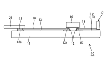
- the top view which shows schematically the structure of the liquid crystal panel which concerns on this invention
- Partial side view showing wiring of LCD panel
- Block diagram schematically showing the configuration of the LCD controller / driver IC
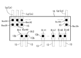
- Plan view schematically showing bump arrangement of LCD controller / driver IC
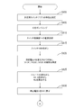
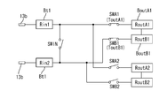
- Equivalent circuit diagram for connection resistance measurement Flow chart showing processing related to input side connection resistance measurement Explanatory drawing showing the state of the measurement switch when measuring input side connection resistance
- Flow chart showing processing related to output side connection resistance measurement Explanatory drawing showing the state of the measurement switch when measuring output side connection resistance
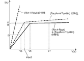
- Graph showing the VI characteristics when measuring output side connection resistance
- FIG. 1 is a plan view schematically showing a configuration of a liquid crystal panel (an example of a display panel) 10 according to the present invention.
- the liquid crystal panel 10 is mounted on, for example, a mobile phone, a PDA, a smartphone, or a tablet-type multifunction mobile terminal device.
- a liquid crystal panel 10 includes a glass substrate 11, a plurality of input wirings (an example of input-side external wiring) 13, a liquid crystal controller / driver IC (an example of an integrated circuit) 16, a liquid crystal display unit 17, a gate.
- Line an example of output-side external wiring
- Ls an example of output-side external wiring
- a source line an example of output-side external wiring
- the liquid crystal panel 10 is, for example, a TFT (Thin Film Transistor) color liquid crystal panel, and displays a color image according to a liquid crystal drive signal (an example of an output signal) from the liquid crystal controller / driver 16.
- the liquid crystal display unit 17 includes a plurality of pixels including a TFT and a liquid crystal cell LC, a color filter (not shown), a filter side substrate, and the like.
- the liquid crystal controller / driver IC 16 may be simply a liquid crystal driver, and the liquid crystal controller may not be included in the liquid crystal panel 10. Further, the liquid crystal panel 10 may include a backlight device.
- a plurality of input wirings 13 made of, for example, ITO, a plurality of gate lines Lg, and a plurality of source lines Ls are sized, that is, display pixels. It is formed according to the number of numbers.
- An FPC pad 13a for connecting to an FPC (flexible substrate) 21 is formed at one end of each input wiring 13, and an IC pad for connecting to the input side pump Bin of the IC 16 at the other end of each input wiring 13.
- a portion 13b is formed.
- each gate line Lg and source line Ls an IC pad portion 15 for connecting to the output side pump pair BPout of the IC 16 is formed.
- a gate signal (common line selection signal) Sg applied to the gate of the TFT corresponding to each pixel in the liquid crystal display unit 17 is supplied from the IC 16 to each gate line Lg.
- a source signal (gradation signal) Ss to be applied to the source of the TFT is supplied from the IC 16 to each source line Ls.
- the FPC 21 and the FPC pad 13a, the input side pump Bin and the IC pad unit 13b, and the output side pump Bout and the IC pad unit 15 are anisotropic in the present embodiment. They are electrically connected by the conductive material 12.
- FIG. 3 is a block diagram schematically showing the configuration of the IC 16
- FIG. 4 is a plan view schematically showing the bump arrangement of the IC 16.
- the IC 16 has a connection resistance measurement function in a state where it is connected to the input wiring 13, the gate line Lg, and the source line Ls.
- the IC 16 includes a plurality of input side pump bins (an example of an input terminal unit), a switch control unit 20, an output signal generation unit 30, a plurality of output side pump pairs (an example of an output terminal pair unit) BPout, and a measurement signal terminal unit Bt1, Bt2, a plurality of output switches QA and QB, a first measurement switch SWIN, a plurality of second measurement switches SWA and SWB, and the like.
- each measurement switch is composed of an FET as shown in FIG.
- Each measurement switch is not limited to an FET.
- the first measurement switch (first field effect transistor) SWIN is provided between a pair of measurement signal input bumps (an example of a measurement signal terminal portion) Bt1 and Bt2.
- Each second measurement switch (second field effect transistor) SWA is provided between the measurement signal input bump (one measurement signal terminal part) Bt1 and the output side pump (one output terminal part) BoutA.
- Each of the second measurement switches (third field effect transistors) SWB is provided between the measurement signal input bump (the other measurement signal terminal portion) Bt2 and the output side pump (the other output terminal portion) BoutB.
- the plurality of input side pumps Bin1 to Bin9 are connected to the input side external wiring 13 through the anisotropic conductive material 12 and the IC pad 13b when the IC 16 is mounted on the substrate 11.
- the plurality of output-side pump pairs BPout are output pumps BoutA that output the output signals Sg and Ss to the gate line Lg and the source line Ls during the normal operation of the IC 16, that is, when the IC 16 displays an image on the liquid crystal display unit 17.
- BoutB is configured as a pair.
- each output side pump BoutA and each output side pump BoutB are connected to the IC pad portion 15 of the gate line Lg or the source line Ls via the anisotropic conductive material 12, as shown in FIG.
- the pad portion 15 is short-circuited. That is, when the IC 16 is connected to the substrate 11, the output pump BoutA and the output pump BoutB in each output pump pair BPout are electrically coupled.
- a plurality of output switches QA and QB are provided between the output signal generation unit 30 and the output side pumps BoutA and BoutB.
- Each output switch QA, QB switches the connection state between the output signal generation unit 30 and each output side pump BoutA, BoutB based on the switching control signal U of the output signal generation unit 30 during the normal operation of the IC 16.
- all the output switches QA and QB are turned on during the normal operation of the IC 16, and the output signal W from the output signal generation unit 30 is supplied to the output side pumps BoutA and BoutB.
- the present invention is not limited to this, and one of the output switches QA and QB may be turned on during normal operation.
- the output signal generator 30 generates a plurality of output signals W by performing signal processing according to the input signals input from the plurality of input side pumps Bin5 to Bin9 during the normal operation of the IC 16.
- the input signal includes, for example, a video signal Video, a synchronization signal Sync, a clock signal CLK, a power supply Vdd2, a drive power supply DVdd, and the like.
- the plurality of output signals W include a gate signal Sg and a source signal Ss.
- the output signal generation unit 30 includes signal processing circuits such as an arithmetic circuit and an amplifier circuit (not shown), and generates the source signal Ss based on the video signal Video, the synchronization signal Sync, the clock signal CLK, the drive power supply DVdd, and the like. Further, the output signal generation unit 30 generates the gate signal Sg based on the synchronization signal Sync, the clock signal CLK, the driving power supply DVdd, and the like.
- the output signal generator 30 generates a plurality of switching control signals U that turn on the plurality of output switches QA and QB during normal operation.
- Each switching control signal is supplied to the gate of each output switch QA, QB. That is, during normal operation, the output switches QA and QB are turned on, and the gate signal Sg and the source signal Ss are output from the output side pumps BoutA and BoutB.
- which output switch QA, QB, that is, each output-side pump BoutA, BoutB is supplied with the gate signal Sg or the source signal Ss is appropriately determined according to the pixel configuration of the liquid crystal display unit 17.
- a pair of measurement signal input bumps (an example of a measurement signal terminal portion) Bt1 and Bt2 are connected to the input-side external wiring 13 via the anisotropic conductive material 12 and the IC pad 13b, and the measurement signal is measured when measuring the connection resistance.
- Input and output (measurement voltage and measurement current). Specifically, the measurement voltage V is input from the measurement signal terminal unit Bt1, and the measurement current I due to the application of the measurement voltage V is returned from the measurement signal terminal unit Bt2.
- the first measurement switch SWIN switches the connection state between the pair of measurement signal terminal portions Bt1 and Bt2 when measuring the connection resistance in the IC 16.
- the first control signal Con1, the second control signal Con2, and the power supply Vdd1 are input to the switch control unit 20.
- the switch control unit 20 controls the switching operation of the first measurement switch SWIN and the second measurement switches SWA and SWB based on the first control signal Con1 and the second control signal Con2.
- the first control signal Con1 is, for example, a timing signal that mainly causes the switch control unit 20 to start and end the switch switching operation.
- the second control signal Con2 is, for example, a shift signal for sequentially scanning the output terminal pair BPout to be controlled in order to sequentially measure the resistance of the output terminal pair BPout.
- the switch control unit 20 turns on the first measurement switch SWIN when measuring the connection resistance between the pair of measurement signal input bumps Bt1, Bt2 and the input-side external wiring 13, and The second measurement switches SWA and SWB are turned off.
- the first measurement switch SWIN is turned off and the second measurement switches SWA and SWB are turned on.
- the power source Vdd1 is a power source that is supplied only to the switch control unit 20 when measuring the connection resistance. That is, in the present embodiment, power is not supplied to the output signal generation unit 30 during connection resistance measurement, and the output signal W (gate signal Sg, source signal Ss) and control signal U are not generated. Therefore, the electrical control between the output signal generation unit 30 and each of the output terminal pair parts BPout1 to BPoutn is cut off during connection resistance measurement.
- the first measurement switch SWIN and all the second measurement switches SWA and SWB are turned off, and the connection resistance measurement system is disconnected from the normally operating circuit system (liquid crystal drive circuit system).
- FIG. 5 is a circuit diagram showing an equivalent circuit during connection resistance measurement.
- the measurement power supply 41 is connected to the measurement signal input bumps Bt ⁇ b> 1 and Bt ⁇ b> 2 via a predetermined terminal of the FPC 21 and the input wiring 13.
- an ammeter 42 for measuring the measurement current I is connected in series with the measurement power supply 41 and a voltmeter 43 for measuring the measurement voltage V is connected in parallel with the measurement power supply 41 between the measurement power supply 41 and the FPC 21.
- This connection resistance measurement is used, for example, in connection inspection at the time of IC connection to the substrate 11, re-inspection before shipment, cause analysis of market failure, product durability test, product storage test, and the like.
- the first input connection resistance Rin1 indicates a resistance in a state where the measurement signal input bump Bt1 is connected to the IC pad 13b by the anisotropic conductive material 12. That is, the first input connection resistance Rin1 includes a resistance due to the measurement signal input bump Bt1 and the anisotropic conductive material 12. Similarly, the second input connection resistance Rin2 includes a resistance due to the measurement signal input bump Bt2 and the anisotropic conductive material 12.
- the first output connection resistance RoutA includes a resistance due to the output side pump BoutA and the anisotropic conductive material 12, and the second output connection resistance RoutB includes a resistance due to the output side pump BoutB and the anisotropic conductive material 12. Is included.
- connection resistance first connection resistance: hereinafter simply referred to as input connection resistance
- Rin Rin1 + Rin2.
- FIG. 6 is a flowchart showing processing related to input connection resistance measurement
- FIG. 7 is an explanatory diagram showing the state of each switch during input connection resistance measurement
- FIG. 8 is a graph schematically showing the relationship (VI characteristic) between the measurement voltage V and the measurement current I when measuring the input connection resistance.
- the characteristics of the measurement switches (FETs) SWIN, SWA, SWB are measured at the time of manufacturing each switch (step S100). That is, before each switch is bonded to the glass substrate 11, characteristics (VI characteristics) between the drain-source voltage and the drain-source current are obtained under a predetermined gate voltage (FIG. 8, see FIG. Then, when measuring the connection resistance, a voltage drop due to each measurement switch is estimated using the VI characteristic. From the estimated voltage drop and drain-source current (measurement current), the on-resistances Tin and (ToutA + ToutB) of the measurement switches (FETs) SWIN, SWA, and SWB are determined (calculated).
- the gate voltage for turning on each measurement switch after each measurement switch (FET) SWIN, SWA, SWB is bonded to the glass substrate 11 is the predetermined voltage when acquiring the VI characteristics in advance. It is assumed that the gate voltage is designed to be almost equal to the voltage.
- step S105 the IC 16 is bonded to the IC pads 13b and 15 on the glass substrate 11 using the anisotropic conductive material 12 (step S105).
- the power supply Vdd1 is supplied to the switch control unit 20 through the FPC 21 and the input side pumps Bin3 and Bin4 (step S110).
- control signals Con1 and Con2 are supplied to the switch controller 20 via the FPC 21 and the input side pumps Bin1 and Bin2. Then, according to the control signals Con1 and Con2, as shown in FIG. 7, only the first measurement switch SWIN is turned on (conductive), and the second measurement switch SWA and the second measurement switch SWB are all turned off ( Non-conduction) (step S115).
- the measurement voltage V is applied via the FPC 21 and the measurement signal input bump Bt1. Then, by changing the measurement voltage V, a VI characteristic (Rin + Tin characteristic) indicated by a solid line in FIG. 8 is measured.
- the VI characteristic is measured in consideration of the input connection resistance Rin and the ON resistance Tin of the first measurement switch SWIN. From the VI characteristics, current values I1, I2, and I3 corresponding to the measured voltages V1, V2, and V3 are measured as shown in FIG. 8 (step S120).
- the voltage V1 is an arbitrary voltage value in an increase region where the measurement current I increases in accordance with the measurement voltage V
- the voltage V2 changes from the increase region to a saturation region where the measurement current I is saturated. It is a voltage value
- the voltage V3 is a voltage value in the saturation region.
- the measurement voltage V2 and the measurement current I2 are determined from the point where ⁇ V / ⁇ I or ⁇ I / ⁇ V changes abruptly.
- the voltage V1 is measured at a plurality of locations with a predetermined voltage width ⁇ V.
- the voltage width ⁇ V is, for example, a voltage difference of 0.1 V when the maximum value of the measurement voltage V is 5 V.
- ⁇ I is a current difference corresponding to ⁇ V.
- the input connection resistance Rin is calculated by subtracting the on-resistance Tin from the total resistance value, that is, excluding the on-resistance (step S125).
- the drain-source voltage Vds becomes Vds1 from the intersection of the measured current I2 and the “Tin characteristic”.
- the measurement voltage V is returned to 0 V, and the measurement of the input connection resistance Rin is terminated (step S130).
- FIG. 9 is a flowchart showing a process related to the output connection resistance measurement
- FIG. 10 is an explanatory view showing the state of each switch during the output connection resistance measurement
- FIG. 11 is a graph schematically showing the relationship (VI characteristics) between the measurement voltage V and the measurement current I when measuring the output connection resistance.
- the output connection resistance Rout is measured for each output terminal pair BPout1 to BPoutn. However, since the measurement method is the same, only the output terminal pair BPout1 will be described for convenience of explanation. Note that the output connection resistance Rout is not limited to be measured for all the output terminal pairs BPout1 to BPoutn.
- the output connection resistance Rout may be measured only with respect to a desired output terminal pair BPout, for example, the output terminal pair BPout related to the malfunction.
- the measurement of the output connection resistance Rout is performed subsequent to the measurement of the input connection resistance Rin, and a pair of second measurement switches SWA1 of the output terminal pair BPout1 as shown in FIG. 10 according to the control signals Con1 and Con2. , SWB1 is turned on (conductive), and the first measurement switch SWIN and the second measurement switches SWA, SWB of the other output terminal pair BPout are all turned off (non-conductive) (step S200).
- step S120 the measurement voltage V is applied through the FPC 21 and the measurement signal input bump Bt1. Then, by changing the measurement voltage V, the input connection resistance Rin, the output connection resistance Rout, and the ON resistances ToutA1 and ToutB1 of the second measurement switches SWA1 and SWB1 shown by the solid lines in FIG. Characteristics are measured. From the VI characteristics, as shown in FIG. 11, current values I5, I6, and I7 corresponding to the measured voltages V5, V6, and V7 are measured as in step S120 (step S205).
- the voltage V5 is a voltage value in an increasing region where the measurement current I increases according to the measurement voltage V
- the voltage V6 is a voltage value at a point where the measuring current I changes from the increasing region to a saturation region where the measuring current I is saturated.
- the voltage V7 is a voltage value in the saturation region.
- the measurement voltage V6 and the measurement current I6 are determined from the point where ⁇ V / ⁇ I or ⁇ I / ⁇ V changes abruptly by the same method as in step S125.
- V6 / I6 (total resistance value) Rin + Rout + ToutA1 + ToutB1
- the output resistance Rout is calculated by subtracting the on resistance (ToutA1 + ToutB1) and Rin from the total resistance value (step S210). That is, the output connection resistance Rout is calculated excluding the on-resistance.
- ToutA1 + ToutB1 total value of on-resistance
- Tin total value of on-resistance
- step S220 When measurement of all output connection resistances Rout is completed (step S220: YES), the control signals Con1 and Con2 are set as measurement end signals (step S230), and all measurement switches are turned off (step S230). S235).
- step S220 NO
- the current measurement switches SWA and SWB are turned off, and the next measurement switches SWA and SWB are turned on.
- step S225 the next measurement switches SWA and SWB are turned on.
- the input side connection resistance Rin is measured by turning on the first measurement switch SWIN and turning off the second measurement switches SWA and SWB. Further, the connection resistance obtained by adding the input side connection resistance Rin and the output side connection resistance Rout is measured by turning off the first measurement switch and turning off the second measurement switch. Then, the output side connection resistance Rout is measured by subtracting the input side connection resistance Rin from the added connection resistance. Therefore, the output side connection resistance Rout of the IC 16 can be measured easily and suitably.
- connection resistance Rin, Rout when measuring each connection resistance Rin, Rout, the on-resistance Tin of the first measurement switch SWIN and the on-resistances ToutA, ToutB of the second measurement switches SWA, SWB are subtracted. That is, since the values of the connection resistances Rin and Rout can be measured by excluding (subtracting) the on-resistance of each measurement switch, a more accurate output-side connection resistance value can be obtained. Further, when the connection resistance is measured by subtracting the on-resistance, the point at which the VI characteristic is measured and the measurement current I changes from the increase region to the measurement voltage saturation region is used. Therefore, measurement errors between FETs (measurement switches) can be reduced.
- connection resistance measurement when measuring the connection resistance, power is supplied to the switch control unit 20 via the power input terminal unit, and power supply to the output signal generation unit 30 is stopped. Thereby, the control of the output switches QA and QB is stopped when the connection resistance is measured. Therefore, since the circuit system that performs normal operation is separated from the connection resistance measurement system, the connection resistance measurement can be suitably performed without being affected by the circuit system that performs normal operation. Also, during normal operation, the second measurement switches SWA and SWB are turned off, and the connection resistance measurement system is separated from the circuit system that performs normal operation. Therefore, normal operation is preferably performed without being affected by the connection resistance measurement system. It can be performed.
- connection resistance is calculated in consideration of the on-resistance of the measurement switch. You may make it do.
- the measurement voltages V2, V6 and the measurement currents I2, I6 are determined from the point where ⁇ V / ⁇ I or ⁇ I / ⁇ V changes rapidly, and the measurement voltages V2, V6 and the measurement current I2,
- the present invention is not limited to this.
- the measurement voltages V2 and V6 and the measurement currents I2 and I6, which are the changing points from the increase region to the saturation region are simply obtained from the VI characteristics of FIG. 8 or FIG. May be determined.
- arbitrary measurement voltages V1, V5 and measurement currents I1, I5 in the current increase region are simply determined from the VI characteristics of FIG. 8 or FIG. 9, and the VI characteristics shown in FIG. 8 or FIG. Utilizing this, the drain-source voltage Vds is determined (estimated). Then, the on-resistance may be calculated from the determined drain-source voltage Vds and the measured currents I1 and I5.
- the drain-source connection at a predetermined gate voltage for each FET is performed.
- the present invention is not limited to this.
- the VI characteristics described in the FET specifications may be used without obtaining the VI characteristics in advance.
- the measurement signal terminal unit may be configured by any two input terminal units among the plurality of input terminal units Bin.
- an input switch similar to the output switches QA and QB may be provided to disconnect the input terminal portion Bin used as the measurement signal terminal portion from the internal circuit when measuring the connection resistance.
- input side connection resistances other than the measurement signal terminal portions Bt1 and Bt2 can be measured.
- the present invention is not limited thereto.
- the present invention is applicable to any integrated circuit whose connection resistance is to be measured.
- the liquid crystal panel was illustrated as a display panel, this invention is applicable also to another kind of display panel, for example, EL panel.
Landscapes
- Engineering & Computer Science (AREA)
- Computer Hardware Design (AREA)
- Microelectronics & Electronic Packaging (AREA)
- General Engineering & Computer Science (AREA)
- Physics & Mathematics (AREA)
- General Physics & Mathematics (AREA)
- Semiconductor Integrated Circuits (AREA)
Abstract
集積回路16は、通常動作時に出力信号を出力側外部配線に出力する出力端子部が対を成して構成される出力端子対部(BoutA,BoutB)と、入力側外部配線13と接続されて、接続抵抗測定時に測定信号を入出力する一対の測定信号端子部(Bt1,Bt2)と、接続抵抗測定時に、一対の測定信号端子部間の接続状態を切替える第1測定用スイッチSWINと、接続抵抗測定時に、一対の測定信号端子部(Bt1,Bt2)と出力端子対部(BoutA,BoutB)との接続状態を切替える第2測定用スイッチ(SWA、SWB)と、第1測定用スイッチSWINおよび第2測定用スイッチ(SWA、SWB)の切替え動作を制御するスイッチ制御部20とを備える。
Description
本発明は、集積回路を接続配線に接続した際の接続部の抵抗を測定する技術に関する。
従来、集積回路を接続配線に接続した際の接続部の抵抗を測定する技術として、例えば、特許文献1に記載の技術が知られている。特許文献1では、集積回路のデータ入力端子とデータ入力ラインとの接続抵抗を測定する際に、集積回路のアナログ処理を停止させ、接続抵抗の測定に係るデータ入力端子を基準電圧(グランド)に接続する技術が開示されている。
(発明が解決しようとする課題)
しかしながら、上記特許文献1に開示の技術では、データ入力側に関する接続抵抗値を、簡易かつより正確に測定できるものの、データ出力側に関する抵抗の測定については記載されておらず、データ出力側に関する抵抗の測定についても簡易かつより正確に測定できる技術が所望されていた。
しかしながら、上記特許文献1に開示の技術では、データ入力側に関する接続抵抗値を、簡易かつより正確に測定できるものの、データ出力側に関する抵抗の測定については記載されておらず、データ出力側に関する抵抗の測定についても簡易かつより正確に測定できる技術が所望されていた。
本発明は、このような状況に鑑みてなされたものであり、集積回路のデータ出力側に関する接続抵抗値を、簡易かつ好適に測定できる技術を提供することを目的とする。
(課題を解決するための手段)
上記課題を解決するために、本発明に係る集積回路は、外部配線に接続された状態において前記外部配線との接続抵抗を測定する接続抵抗測定機能を有する集積回路であって、入力側外部配線と接続される複数の入力端子部と、通常動作時に、前記複数の入力端子部から入力される入力信号に応じた信号処理を行うことによって出力信号を生成する出力信号生成部と、通常動作時に前記出力信号を出力側外部配線に出力する出力端子部が対を成して構成される出力端子対部と、前記入力側外部配線と接続されて、接続抵抗測定時に測定信号を入出力する一対の測定信号端子部と、接続抵抗測定時に、前記一対の測定信号端子部間の接続状態を切替える第1測定用スイッチと、接続抵抗測定時に、前記一対の測定信号端子部と前記出力端子対部との接続状態を切替える第2測定用スイッチと、接続抵抗測定時に、前記第1測定用スイッチおよび前記第2測定用スイッチの切替え動作を制御するスイッチ制御部とを備える。
上記課題を解決するために、本発明に係る集積回路は、外部配線に接続された状態において前記外部配線との接続抵抗を測定する接続抵抗測定機能を有する集積回路であって、入力側外部配線と接続される複数の入力端子部と、通常動作時に、前記複数の入力端子部から入力される入力信号に応じた信号処理を行うことによって出力信号を生成する出力信号生成部と、通常動作時に前記出力信号を出力側外部配線に出力する出力端子部が対を成して構成される出力端子対部と、前記入力側外部配線と接続されて、接続抵抗測定時に測定信号を入出力する一対の測定信号端子部と、接続抵抗測定時に、前記一対の測定信号端子部間の接続状態を切替える第1測定用スイッチと、接続抵抗測定時に、前記一対の測定信号端子部と前記出力端子対部との接続状態を切替える第2測定用スイッチと、接続抵抗測定時に、前記第1測定用スイッチおよび前記第2測定用スイッチの切替え動作を制御するスイッチ制御部とを備える。
この構成によれば、第1測定用スイッチおよび第2測定用スイッチのスイッチ制御を適宜行うことによって、集積回路のデータ出力側に関する接続抵抗値を、簡易かつ好適に測定することができる。例えば、第1測定用スイッチをオンさせるとともに、第2測定用スイッチをオフさせることによって入力側接続抵抗を測定する。また、第1測定用スイッチをオフさせるとともに、第2測定用スイッチをオンさせることによって入力側接続抵抗と出力側接続抵抗とが加算された接続抵抗を測定する。加算された接続抵抗から入力側接続抵抗を減算することによって出力側接続抵抗を測定できる。
また、前記スイッチ制御部は、前記一対の測定信号端子部と前記入力側外部配線との間の接続抵抗を測定する際に、前記第1測定用スイッチをオンさせるとともに、前記第2測定用スイッチをオフさせ、前記出力端子対部と前記出力側外部配線との間の接続抵抗を測定する際に、前記第1測定用スイッチをオフさせるとともに、前記第2測定用スイッチをオンさせるようにしてもよい。本構成によれば、集積回路のデータ出力側に関する接続抵抗値を、簡易かつ好適に測定することができる。
また、前記第1測定用スイッチは、前記一対の測定信号端子部間に設けられた第1電界効果トランジスタによって構成され、前記第2測定用スイッチは、一方の測定信号端子部と一方の出力端子部との間に設けられた第2電界効果トランジスタと、他方の測定信号端子部と他方の出力端子部との間に設けられた第3電界効果トランジスタとによって構成されるようにしてもよい。この構成によれば、電界効果トランジスタのV-I特性から推定される電界効果トランジスタの電圧降下と、接続抵抗測定時に電界効果トランジスタに流れる電流(測定電流)とから電界効果トランジスタのオン抵抗を算出できる。そのため、電界効果トランジスタのオン抵抗を除いて接続抵抗値を測定することができ、より正確な出力側接続抵抗値を得ることができる。
また、前記測定信号端子部は、前記複数の入力端子部のうちいずれか2個の入力端子部によって構成されるようにしてもよい。この構成によれば、測定信号端子部に限らず、入力端子部に係る接続抵抗を測定することができる。
また、前記出力信号生成部と各出力端子部との間に設けられ、通常動作時において、前記出力信号生成部の制御によって前記出力信号生成部と各出力端子部との接続状態を切替える複数の出力スイッチをさらに備え、複数の入力端子部は、接続抵抗測定時に、前記スイッチ制御部に電源を供給し、前記出力信号生成部へは電源を供給しない電源入力端子部を含むようにしてもよい。この構成によれば、接続抵抗測定時に、通常動作を行う回路系は接続抵抗測定系と分離されるため、通常動作を行う回路系の影響を受けずに、好適に接続抵抗測定を行うことができる。
また、前記集積回路は、液晶パネルを駆動する液晶駆動用集積回路であり、前記出力信号生成部は前記入力信号に応じて、前記出力信号として前記液晶パネルを駆動する液晶駆動信号を生成するようにしてもよい。
また、上記集積回路を表示用集積回路として備えて表示パネルを構成してもよい。この構成によれば、表示用集積回路の接続抵抗を測定することによって表示パネルの歩留まりを向上できる。
また、前記表示パネルは液晶パネルであり、前記出力信号は前記液晶パネルを駆動する液晶駆動信号であるようにしてもよい。この構成によれば、液晶パネルの歩留まりを向上できる。
また、本発明に係る接続抵抗測定方法は、外部配線に接続された状態において前記外部配線との接続抵抗を測定する接続抵抗測定機能を有する集積回路において、接続抵抗を測定する方法であって、入力側外部配線と接続されて測定信号を入出力する一対の測定信号端子部と、前記一対の測定信号端子部間の接続状態を切替える第1測定用スイッチと、前記一対の測定信号端子部と前記出力端子対部との接続状態を切替える第2測定用スイッチとを前記集積回路に設ける工程と、前記集積回路を前記外部配線に接続する接続工程と、前記第1測定用スイッチをオンさせるとともに、第2測定用スイッチをオフさせた状態で、前記測定信号を前記一対の測定信号端子部に供給し、前記一対の測定信号端子部間の電圧と、前記一対の測定信号端子部間に流れる電流とを測定し、測定電圧および測定電流に基づいて、前記一対の測定信号端子部と前記入力側外部配線との間の第1接続抵抗を測定する第1測定工程と、前記第1測定用スイッチをオフさせるとともに、第2測定用スイッチをオンさせた状態で、前記測定信号を前記一対の測定信号端子部に供給し、前記一対の測定信号端子部間の電圧と、前記一対の測定信号端子部間に流れる電流とを測定し、測定電圧、測定電流および前記第1接続抵抗に基づいて、前記出力端子対部と前記出力側外部配線との間の第2接続抵抗を測定する第2測定工程とを含む。
上記測定方法において、前記第1測定用スイッチは、前記一対の測定信号端子部間に設けられた第1電界効果トランジスタによって構成し、前記第2測定用スイッチは、一方の測定信号端子部と一方の出力端子部との間に設けられた第2電界効果トランジスタと、他方の測定信号端子部と他方の出力端子部との間に設けられた第3電界効果トランジスタとによって構成する工程と、前記第1測定工程および第2測定工程は、オンされた電界効果トランジスタのドレイン-ソース間の電圧-電流特性を利用して、前記オンされた電界効果トランジスタによる電圧降下を推定する工程と、推定された前記電圧降下と前記測定電流とから、前記オンされた電界効果トランジスタのオン抵抗を算出する工程と、前記第1接続抵抗あるいは前記第2接続抵抗を測定する際に、算出された前記オン抵抗を除く工程とを含むようにしてもよい。
また、上記測定方法において、前記接続工程の前において、各電界効果トランジスタに関する、所定のゲート電圧におけるドレイン-ソース間の電圧-電流特性を取得する工程と、前記第1測定工程および第2測定工程において、オンされる電界効果トランジスタを、前記所定のゲート電圧によってオンする工程とをさらに含むようにしてもよい。この場合、より正確に電界効果トランジスタのオン抵抗による電圧降下を推定できる。
また、上記測定方法において、前記接続工程の前において、各電界効果トランジスタに関する、所定のゲート電圧におけるドレイン-ソース間の電圧-電流特性を取得する工程と、前記第1測定工程および第2測定工程において、オンされる電界効果トランジスタを、前記所定のゲート電圧によってオンする工程とをさらに含むようにしてもよい。この場合、より正確に電界効果トランジスタのオン抵抗による電圧降下を推定できる。
また、上記測定方法において、前記集積回路は、通常動作時に、前記複数の入力端子部から入力される入力信号に応じた信号処理を行うことによって出力信号を生成する出力信号生成部と、前記出力信号生成部と各出力端子部との間に設けられ、通常動作時において、前記出力信号生成部の制御によって、前記出力信号生成部と各出力端子部との接続状態を切替える複数の出力スイッチとを備え、該方法は、接続抵抗測定時において、前記出力信号生成部への電源供給を停止する工程を含むようにしてもよい。
(発明の効果)
本発明によれば、集積回路のデータ出力側に関する接続抵抗値を、簡易かつ好適に測定できる。
本発明によれば、集積回路のデータ出力側に関する接続抵抗値を、簡易かつ好適に測定できる。
本発明に係る一実施形態を、図1から図11を参照して説明する。
1.液晶パネルの構成
図1は、本発明に係る液晶パネル(表示パネルの一例)10の構成を概略的に示す平面図である。液晶パネル10は、例えば、携帯電話、PDA、スマートフォン、タブレット型多機能携帯端末装置に搭載される。図1に示されるように、液晶パネル10は、ガラス基板11、複数の入力配線(入力側外部配線の一例)13、液晶コントローラ・ドライバIC(集積回路の一例)16、液晶表示部17、ゲート線(出力側外部配線の一例)Lg、およびソース線(出力側外部配線の一例)Ls等を含む。
図1は、本発明に係る液晶パネル(表示パネルの一例)10の構成を概略的に示す平面図である。液晶パネル10は、例えば、携帯電話、PDA、スマートフォン、タブレット型多機能携帯端末装置に搭載される。図1に示されるように、液晶パネル10は、ガラス基板11、複数の入力配線(入力側外部配線の一例)13、液晶コントローラ・ドライバIC(集積回路の一例)16、液晶表示部17、ゲート線(出力側外部配線の一例)Lg、およびソース線(出力側外部配線の一例)Ls等を含む。
液晶パネル10は、本実施形態では、例えば、TFT(Thin Film Transistor)カラー液晶パネルであり、液晶コントローラ・ドライバ16からの液晶駆動信号(出力信号の一例)に応じて、カラー画像を表示する。液晶表示部17はTFTおよび液晶セルLCを含む複数の画素、図示しないカラーフィルタおよびフィルタ側基板等を含む。
なお、液晶コントローラ・ドライバIC16(以下、単にIC16と記す)は単に液晶ドライバとし、液晶コントローラは液晶パネル10に含まれない構成であってもよい。また、液晶パネル10はバックライト装置を含んでもよい。
図2に示されるように、ガラス基板11上には、例えばITOからなる複数の入力配線13、複数のゲート線Lg、および複数のソース線Lsが、液晶表示部17の大きさ、すなわち表示画素数の数に応じて形成されている。
各入力配線13の一端にはFPC(フレキシブル基板)21と接続するためのFPC用パッド13aが形成され、各入力配線13の他端にはIC16の入力側パンプBinと接続するためのIC用パッド部13bが形成されている。
また、各ゲート線Lgおよびソース線Lsの一端には、IC16の出力側パンプ対BPoutと接続するためのIC用パッド部15が形成されている。そして、各ゲート線Lgには、液晶表示部17内の各画素に対応するTFTのゲートに印加するゲート信号(コモンライン選択信号)SgがIC16から供給される。各ソース線Lsには、TFTのソースに印加するソース信号(階調信号)SsがIC16から供給される。
また、図2に示されるように、FPC21とFPC用パッド13a、入力側パンプBinとIC用パッド部13b、出力側パンプBoutとIC用パッド部15とは、本実施形態では、それぞれ異方性導電材12によって電気的に接続される。
2.液晶コントローラ・ドライバICの構成
次に図3および図4を参照して、IC16を説明する。図3はIC16の構成を概略的に示すブロック図であり、図4は、IC16のバンプ配置を概略的に示す平面図である。
次に図3および図4を参照して、IC16を説明する。図3はIC16の構成を概略的に示すブロック図であり、図4は、IC16のバンプ配置を概略的に示す平面図である。
IC16は、入力配線13、ゲート線Lg、およびソース線Lsに接続された状態において、接続抵抗測定機能を有する。IC16は、複数の入力側パンプBin(入力端子部の一例)、スイッチ制御部20、出力信号生成部30、複数の出力側パンプ対(出力端子対部の一例)BPout、測定信号端子部Bt1,Bt2、複数の出力スイッチQA,QB、第1測定用スイッチSWIN、複数の第2測定用スイッチSWA,SWB等を含む。本実施形態において、各測定用スイッチは、図3に示されるようにFETによって構成されている。なお、各測定用スイッチはFETに限られない。
第1測定用スイッチ(第1電界効果トランジスタ)SWINは、一対の測定信号入力バンプ(測定信号端子部の一例)Bt1,Bt2間に設けられている。また、各第2測定用スイッチ(第2電界効果トランジスタ)SWAは、測定信号入力バンプ(一方の測定信号端子部)Bt1と出力側パンプ(一方の出力端子部)BoutAとの間に設けられ、各第2測定用スイッチ(第3電界効果トランジスタ)SWBは、測定信号入力バンプ(他方の測定信号端子部)Bt2と出力側パンプ(他方の出力端子部)BoutBとの間に設けられている。
複数の入力側パンプBin1~Bin9は、IC16が基板11に搭載される際に、異方性導電材12およびIC用パッド13bを介して入力側外部配線13に接続される。
複数の出力側パンプ対BPoutは、IC16の通常動作時に、すなわちIC16が液晶表示部17に画像を表示させる時に、出力信号Sg、Ssをゲート線Lgおよびソース線Lsに出力する出力側パンプBoutAおよびBoutBが対を成して構成される。各出力側パンプBoutAと各出力側パンプBoutBは、ゲート線Lgあるいはソース線LsのIC用パッド部15と異方性導電材12を介して接続された場合、図4に示されるように、IC用パッド部15によって短絡される。すなわち、IC16が基板11に接続されると、各出力側パンプ対BPout内の出力側パンプBoutAと出力側パンプBoutBは電気的に結合される。
また、複数の出力スイッチQA,QBが、出力信号生成部30と各出力側パンプBoutA,BoutBとの間に設けられる。各出力スイッチQA,QBは、IC16の通常動作時において、出力信号生成部30の切替制御信号Uに基づいて、出力信号生成部30と各出力側パンプBoutA,BoutBとの接続状態を切替える。例えば、全ての出力スイッチQA,QBがIC16の通常動作時においてオンされ、出力信号生成部30からの出力信号Wが各出力側パンプBoutA,BoutBに供給される。なお、これに限られず、通常動作時に出力スイッチQA,QBのいずれか一方をオンするようにしてもよい。
出力信号生成部30は、IC16の通常動作時に、複数の入力側パンプBin5~Bin9から入力される入力信号に応じた信号処理を行うことによって複数の出力信号Wを生成する。入力信号には、図3に示されるように、例えば、映像信号Video、同期信号Sync、クロック信号CLK、電源Vdd2および駆動用電源DVdd等が含まれる。また、複数の出力信号Wには、ゲート信号Sgおよびソース信号Ssが含まれる。
出力信号生成部30は、図示しない演算回路および増幅回路等の信号処理回路を含み、映像信号Video、同期信号Sync、クロック信号CLK、および駆動用電源DVdd等に基づいてソース信号Ssを生成する。また、出力信号生成部30は、同期信号Sync、クロック信号CLK、および駆動用電源DVdd等に基づいてゲート信号Sgを生成する。
さらに、出力信号生成部30は、通常動作時に、複数の出力スイッチQA,QBをオンする複数の切替制御信号Uを生成する。各切替制御信号は、各出力スイッチQA,QBのゲートに供給される。すなわち、通常動作時には出力スイッチQA,QBがオンされて、各出力側パンプBoutA,BoutBからゲート信号Sgおよびソース信号Ssが出力される。なお、ゲート信号Sgあるいはソース信号Ssを、いずれの出力スイッチQA,QB、すなわち、各出力側パンプBoutA,BoutBに供給するかは、液晶表示部17の画素構成に応じて適宜決定される。
また、一対の測定信号入力バンプ(測定信号端子部の一例)Bt1,Bt2は、異方性導電材12およびIC用パッド13bを介して入力側外部配線13に接続され、接続抵抗測定時に測定信号(測定電圧および測定電流)を入出力する。具体的には、測定信号端子部Bt1から測定電圧Vが入力され、測定信号端子部Bt2から測定電圧Vの印加による測定電流Iが戻る。
第1測定用スイッチSWINは、IC16における接続抵抗測定時に、一対の測定信号端子部Bt1,Bt2間の接続状態を切替える。
スイッチ制御部20には、第1制御信号Con1、第2制御信号Con2および電源Vdd1が入力される。スイッチ制御部20は、第1制御信号Con1および第2制御信号Con2に基づいて、第1測定用スイッチSWINおよび第2測定用スイッチSWA,SWBの切替え動作を制御する。第1制御信号Con1は、例えば、主にスイッチ制御部20にスイッチ切替え動作を開始および終了させるタイミング信号である。第2制御信号Con2は、例えば、出力端子対部BPoutの抵抗測定を順次行うために、制御する出力端子対部BPoutを順に走査させるシフト信号である。
具体的には、スイッチ制御部20は、一対の測定信号入力バンプBt1,Bt2と入力側外部配線13との間の接続抵抗を測定する際には、第1測定用スイッチSWINをオンさせるとともに、第2測定用スイッチSWA,SWBをオフさせる。一方、出力端子対部BPoutと出力側外部配線Lg、Lsとの間の接続抵抗を測定する際に、第1測定用スイッチSWINをオフさせるとともに、第2測定用スイッチSWA,SWBをオンさせる。
電源Vdd1は、接続抵抗測定時に、スイッチ制御部20のみに供給する電源である。すなわち、本実施形態においては、接続抵抗測定時に出力信号生成部30には電源が供給されず、出力信号W(ゲート信号Sg、ソース信号Ss)および制御信号Uは生成されない。そのため、接続抵抗測定時に、出力信号生成部30と各出力端子対部BPout1~BPoutnとの電気的制御は遮断される。
一方、通常動作時には、第1測定用スイッチSWINおよび全ての第2測定用スイッチSWA,SWBはオフされ、接続抵抗測定系は通常動作する回路系(液晶駆動回路系)とは遮断される。
3.接続抵抗測定
次に、本実施形態における接続抵抗測定を図5から図11を参照して説明する。図5は、接続抵抗測定時の等価回路を示す回路図である。図5に示されるように、接続抵抗測定時、FPC21の所定の端子および入力配線13を介して測定信号入力バンプBt1,Bt2に測定電源41が接続される。また、測定電源41とFPC21との間において、測定電流Iを計測する電流計42が測定電源41と直列に接続され、測定電圧Vを計測する電圧計43が測定電源41と並列に接続される。なお、本接続抵抗測定は、例えば、基板11へのIC接続時の接続検査、出荷前の再検査、市場不良の原因解析、製品耐久試験、および製品保管試験等において利用される。
次に、本実施形態における接続抵抗測定を図5から図11を参照して説明する。図5は、接続抵抗測定時の等価回路を示す回路図である。図5に示されるように、接続抵抗測定時、FPC21の所定の端子および入力配線13を介して測定信号入力バンプBt1,Bt2に測定電源41が接続される。また、測定電源41とFPC21との間において、測定電流Iを計測する電流計42が測定電源41と直列に接続され、測定電圧Vを計測する電圧計43が測定電源41と並列に接続される。なお、本接続抵抗測定は、例えば、基板11へのIC接続時の接続検査、出荷前の再検査、市場不良の原因解析、製品耐久試験、および製品保管試験等において利用される。
図5において、第1入力接続抵抗Rin1は、測定信号入力バンプBt1が異方性導電材12によってIC用パッド13bに接続された状態の抵抗を示す。すなわち、第1入力接続抵抗Rin1には、測定信号入力バンプBt1および異方性導電材12による抵抗が含まれる。同様に、第2入力接続抵抗Rin2には、測定信号入力バンプBt2および異方性導電材12による抵抗が含まれる。また、第1出力接続抵抗RoutAには、出力側パンプBoutAおよび異方性導電材12による抵抗が含まれ、第2出力接続抵抗RoutBには、出力側パンプBoutBおよび異方性導電材12による抵抗が含まれる。
3-1.測定信号入力側の接続抵抗測定
まず、図6から図8を参照して測定信号入力側の接続抵抗の測定について説明する。測定信号入力側の接続抵抗(第1接続抵抗:以下、単に入力接続抵抗という)Rinは、第1入力接続抵抗Rin1と第2入力接続抵抗Rin2との合計であり、Rin=Rin1+Rin2 となる。
まず、図6から図8を参照して測定信号入力側の接続抵抗の測定について説明する。測定信号入力側の接続抵抗(第1接続抵抗:以下、単に入力接続抵抗という)Rinは、第1入力接続抵抗Rin1と第2入力接続抵抗Rin2との合計であり、Rin=Rin1+Rin2 となる。
図6は入力接続抵抗測定に係る処理を示すフローチャートであり、図7は入力接続抵抗測定時の各スイッチの状態を示す説明図である。図8は入力接続抵抗測定時の測定電圧Vと測定電流Iとの関係(V-I特性)を概略的に示すグラフである。
入力接続抵抗Rinの測定においては、図6に示されるように、まず、測定用スイッチ(FET)SWIN、SWA、SWBの特性が、各スイッチの製造時等において測定される(ステップS100)。すなわち、各スイッチがガラス基板11にボンディングされる前に、所定のゲート電圧のもとで、ドレイン-ソース間電圧とドレイン-ソース間電流との特性(V-I特性)が取得される(図8、図11参照)。そして、接続抵抗測定の際に、V-I特性を利用して、各測定用スイッチによる電圧降下が推定される。推定された電圧降下とドレイン-ソース間電流(測定電流)から、各測定用スイッチ(FET)SWIN、SWA、SWBのオン抵抗Tin、(ToutA+ToutB)が決定(算出)される。
なお、各測定用スイッチ(FET)SWIN、SWA、SWBがガラス基板11にボンディングされた後における、各測定用スイッチをオンするゲート電圧は、事前にV-I特性を取得する際の上記所定のゲート電圧と、ほぼ等しい電圧となるように設計されているものとする。
なお、各測定用スイッチ(FET)SWIN、SWA、SWBがガラス基板11にボンディングされた後における、各測定用スイッチをオンするゲート電圧は、事前にV-I特性を取得する際の上記所定のゲート電圧と、ほぼ等しい電圧となるように設計されているものとする。
次いで、IC16が、ガラス基板11上のIC用パッド部13b,15に異方性導電材12を用いてボンディングされる(ステップS105)。次いで、FPC21および入力側パンプBin3,Bin4を介して、スイッチ制御部20に電源Vdd1が供給される(ステップS110)。
続いて、FPC21および入力側パンプBin1,Bin2を介して、スイッチ制御部20に制御信号Con1,Con2が供給される。そして、制御信号Con1,Con2にしたがって、図7に示されるように、第1測定用スイッチSWINのみがオン(導通)とされ、第2測定用スイッチSWAおよび第2測定用スイッチSWBは全てオフ(非導通)とされる(ステップS115)。
次いで、FPC21および測定信号入力バンプBt1を介して測定電圧Vが印加される。そして、測定電圧Vを変化させて、図8に実線で示されるV-I特性(Rin+Tinの特性)が測定される。Rin+Tinの特性では、入力接続抵抗Rinと第1測定用スイッチSWINのオン抵抗Tinが加味された、V-I特性が測定される。そのV-I特性から、図8に示されるように、測定電圧V1、V2、V3に対応した電流値I1、I2、I3が測定される(ステップS120)。ここで、電圧V1は、測定電流Iが測定電圧Vに応じて増加する増加領域内の任意の電圧値であり、電圧V2は増加領域から測定電流Iが飽和する飽和領域へ変化する点での電圧値であり、電圧V3は飽和領域内の電圧値である。
その際、本実施形態においては、ΔV/ΔIあるいはΔI/ΔVが急激に変化する点から、測定電圧V2および測定電流I2を決定する。この場合、増加領域(0V-V2近傍)において、電圧V1が所定の電圧幅ΔVで複数箇所、測定される。なお、ここで、電圧幅ΔVは、例えば、測定電圧Vの最大値を5Vとすると、0.1Vの電圧差とされる。ΔIはそのΔVに対応した電流差とされる。
そして、V2/I2(合計抵抗値)=Rin+Tin
の関係から、合計抵抗値からオン抵抗Tinを差し引いて、すなわち、オン抵抗分を除外して、入力接続抵抗Rinが算出される(ステップS125)
ここで、オン抵抗Tinは、第1測定用スイッチSWINの電圧降下、すなわち、ドレイン-ソース電圧Vdsと、測定電流I2とから、Tin=Vds/I2によって算出される。なお、ドレイン-ソース電圧Vdsは、図8において、測定電流I2と「Tinの特性」との交点から、Vds1となる。
次いで測定電圧Vを0Vに戻して、入力接続抵抗Rinの測定を終了する(ステップS130)。
そして、V2/I2(合計抵抗値)=Rin+Tin
の関係から、合計抵抗値からオン抵抗Tinを差し引いて、すなわち、オン抵抗分を除外して、入力接続抵抗Rinが算出される(ステップS125)
ここで、オン抵抗Tinは、第1測定用スイッチSWINの電圧降下、すなわち、ドレイン-ソース電圧Vdsと、測定電流I2とから、Tin=Vds/I2によって算出される。なお、ドレイン-ソース電圧Vdsは、図8において、測定電流I2と「Tinの特性」との交点から、Vds1となる。
次いで測定電圧Vを0Vに戻して、入力接続抵抗Rinの測定を終了する(ステップS130)。
3-2.信号出力側の接続抵抗測定
次いで、図9から図11を参照して信号出力側の接続抵抗の測定について説明する。信号出力側の接続抵抗(第2接続抵抗:以下、単に出力接続抵抗という)Routは、第1出力接続抵抗RoutAと第2出力接続抵抗RoutBとの合計であり、
Rout=RoutA+RoutB となる。
次いで、図9から図11を参照して信号出力側の接続抵抗の測定について説明する。信号出力側の接続抵抗(第2接続抵抗:以下、単に出力接続抵抗という)Routは、第1出力接続抵抗RoutAと第2出力接続抵抗RoutBとの合計であり、
Rout=RoutA+RoutB となる。
図9は出力接続抵抗測定に係る処理を示すフローチャートであり、図10は出力接続抵抗測定時の各スイッチの状態を示す説明図である。図11は出力接続抵抗測定時の測定電圧Vと測定電流Iとの関係(V-I特性)を概略的に示すグラフである。なお、出力接続抵抗Routの測定は、各出力端子対部BPout1~BPoutnについて行われるが、測定方法は同一のため、説明の便宜上、出力端子対部BPout1についてのみ説明する。なお、全ての出力端子対部BPout1~BPoutnについて出力接続抵抗Routが測定されることには限定されない。所望の出力端子対部BPout、例えば、不具合に関連した出力端子対部BPoutに関してのみ出力接続抵抗Routを測定するようにしてもよい。
出力接続抵抗Routの測定は、入力接続抵抗Rinの測定に引き続いて行われ、制御信号Con1,Con2にしたがって、図10に示されるように、出力端子対部BPout1の一対の第2測定用スイッチSWA1、SWB1のみがオン(導通)とされ、第1測定用スイッチSWINおよび他の出力端子対部BPoutの第2測定用スイッチSWA、SWBは全てオフ(非導通)とされる(ステップS200)。
次いで、ステップS120と同様に、FPC21および測定信号入力バンプBt1を介して測定電圧Vが印加される。そして、測定電圧Vを変化させて、図11に実線で示される、入力接続抵抗Rin、出力接続抵抗Rout、第2測定用スイッチSWA1、SWB1のオン抵抗ToutA1,ToutB1が加味された、V-I特性が測定される。そのV-I特性から、図11に示されるように、ステップS120と同様に、測定電圧V5、V6、V7に対応した電流値I5、I6、I7が測定される(ステップS205)。ここで、電圧V5は、測定電流Iが測定電圧Vに応じて増加する増加領域の電圧値であり、電圧V6は増加領域から測定電流Iが飽和する飽和領域へ変化する点での電圧値であり、電圧V7は飽和領域の電圧値である。
次いで、ステップS125と同様な方法で、ΔV/ΔI、あるいはΔI/ΔVが急激に変化する点から、測定電圧V6および測定電流I6を決定する。そして、V6/I6(合計抵抗値)=Rin+Rout+ToutA1+ToutB1
の関係から、合計抵抗値からオン抵抗(ToutA1+ToutB1)とRinとを差し引いて、出力接続抵抗Routが算出される(ステップS210)。すなわち、オン抵抗分を除外して、出力接続抵抗Routが算出される。ここで、ToutA1+ToutB1(オン抵抗の合計値)は、オン抵抗Tinと同様に算出される。すなわち、第2測定用スイッチSWA1、SWB1による電圧降下、すなわち、ドレイン-ソース電圧Vdsの合計値は、図11において、測定電流I6と「ToutA+ToutBの特性」との交点から、Vds2となる。そして、Vds2=(ToutA1+ToutB1)*I6の関係から、ToutA1+ToutB1が算出される。
の関係から、合計抵抗値からオン抵抗(ToutA1+ToutB1)とRinとを差し引いて、出力接続抵抗Routが算出される(ステップS210)。すなわち、オン抵抗分を除外して、出力接続抵抗Routが算出される。ここで、ToutA1+ToutB1(オン抵抗の合計値)は、オン抵抗Tinと同様に算出される。すなわち、第2測定用スイッチSWA1、SWB1による電圧降下、すなわち、ドレイン-ソース電圧Vdsの合計値は、図11において、測定電流I6と「ToutA+ToutBの特性」との交点から、Vds2となる。そして、Vds2=(ToutA1+ToutB1)*I6の関係から、ToutA1+ToutB1が算出される。
次いで、測定電圧Vを0Vに戻す(ステップS215)。そして、全ての出力接続抵抗Routの測定が終了した場合には(ステップS220:YES)、制御信号Con1,Con2を測定終了の信号に設定し(ステップS230)、測定用スイッチを全てオフさせる(ステップS235)。
一方、全ての出力接続抵抗Routの測定が終了していない場合には(ステップS220:NO)、今回測定用のスイッチSWA、SWBをオフして、次回測定用のスイッチSWA、SWBをオンしてステップS205の処理に戻る(ステップS225)。
4.実施形態の効果
上記したように、本実施形態においては、第1測定用スイッチSWINをオンさせるとともに、第2測定用スイッチSWA,SWBをオフさせることによって入力側接続抵抗Rinが測定される。また、第1測定用スイッチをオフさせるとともに、第2測定用スイッチをオフさせることによって入力側接続抵抗Rinと出力側接続抵抗Routとが加算された接続抵抗が測定される。そして、加算された接続抵抗から入力側接続抵抗Rinを減算することによって出力側接続抵抗Routが測定される。そのため、IC16の出力側接続抵抗Routを、簡易かつ好適に測定できる。
上記したように、本実施形態においては、第1測定用スイッチSWINをオンさせるとともに、第2測定用スイッチSWA,SWBをオフさせることによって入力側接続抵抗Rinが測定される。また、第1測定用スイッチをオフさせるとともに、第2測定用スイッチをオフさせることによって入力側接続抵抗Rinと出力側接続抵抗Routとが加算された接続抵抗が測定される。そして、加算された接続抵抗から入力側接続抵抗Rinを減算することによって出力側接続抵抗Routが測定される。そのため、IC16の出力側接続抵抗Routを、簡易かつ好適に測定できる。
また、各接続抵抗Rin,Routを測定する際に、第1測定用スイッチSWINのオン抵抗Tin、および第2測定用スイッチSWA,SWBのオン抵抗ToutA,ToutBが差し引かれる。すなわち、各測定用スイッチのオン抵抗を除外して(差し引いて)各接続抵抗Rin,Routの値を測定することができるため、より正確な出力側接続抵抗値を得ることができる。また、オン抵抗を差し引いて接続抵抗を測定する際に、V-I特性を測定し、測定電流Iが増加領域から測定電飽和領域へ変化する点が利用される。そのため、FET(測定用スイッチ)間の測定誤差を低減させることできる。また、その際、ΔV/ΔIが急激に変化する点、あるいはΔI/ΔVが急激に変化する点が利用される。そのため、V-I特性における電流増加領域の任意の一点を利用する場合と比べ、FETによる電圧降下分の検出精度が向上され、それによって、接続抵抗測定の精度が向上される。
また、接続抵抗測定時に、電源入力端子部を介してスイッチ制御部20に電源が供給され、出力信号生成部30への電源供給は停止される。それにより、接続抵抗測定時に、出力スイッチQA,QBの制御は停止される。そのため、通常動作を行う回路系は接続抵抗測定系と分離されるため、通常動作を行う回路系の影響を受けずに、好適に接続抵抗測定を行うことができる。また、通常動作時に、第2測定用スイッチSWA,SWBはオフされ、接続抵抗測定系は通常動作を行う回路系と分離されるため、接続抵抗測定系の影響を受けずに、好適に通常動作を行うことができる。
<他の実施形態>
本発明は上記記述及び図面によって説明した実施形態に限定されるものではなく、例えば次のような実施形態も本発明の技術的範囲に含まれる。
本発明は上記記述及び図面によって説明した実施形態に限定されるものではなく、例えば次のような実施形態も本発明の技術的範囲に含まれる。
(1)上記実施形態においては、測定用スイッチのオン抵抗を加味して接続抵抗を算出する例を示したが、これに限られず、測定用スイッチのオン抵抗を加味せずに接続抵抗を算出するようにしてもよい。
(2)上記実施形態においては、ΔV/ΔIあるいはΔI/ΔVが、急激に変化する点から、測定電圧V2,V6および測定電流I2,I6を決定し、測定電圧V2,V6および測定電流I2,I6から、ドレイン-ソース間電圧Vds、すなわち、オン抵抗を算出する例を示したが、これに限られない。例えば、ΔV/ΔIあるいはΔI/ΔVを求めることなく、単に、図8あるいは図9のV-I特性から、増加領域から飽和領域への変化点である測定電圧V2,V6および測定電流I2,I6を決定してもよい。あるいは、単に、図8あるいは図9のV-I特性から、電流増加領域における任意の測定電圧V1,V5および測定電流I1,I5を決定し、図8あるいは図9に示されるV-I特性を利用して、ドレイン-ソース間電圧Vdsを決定(推定)する。そして、決定されたドレイン-ソース間電圧Vdsおよび測定電流I1,I5からオン抵抗を算出するようにしてもよい。
(3)上記実施形態においては、FETのオン抵抗による電圧降下を推定する際に、IC16を基板11に接続する(接続工程)前において、各FETに関する、所定のゲート電圧におけるドレイン-ソース間のV-I特性を取得する例を示したが、これに限られない。事前にV-I特性を取得せずに、例えば、FETの仕様書に記載されたV-I特性を利用するようにしてもよい。
(4)上記実施形態においては、一対の測定信号端子部Bt1,Bt2を複数の入力端子部Binとは個別に設ける例を示したがこれに限られない。測定信号端子部を、複数の入力端子部Binのうちいずれか2個の入力端子部によって構成するようにしてもよい。この場合には、測定信号端子部として使用される入力端子部Binを、接続抵抗測定時に内部回路と切り離す、出力スイッチQA,QBと同様な入力スイッチを設けるようにすればよい。この場合、測定信号端子部Bt1,Bt2以外の入力側接続抵抗の測定が可能になる。
(5)上記実施形態では、集積回路として液晶コントローラ・ドライバICに本発明を適用する例を示したが、これに限られない。本発明は、接続抵抗を測定したい如何なる集積回路にも適応できる。また、表示パネルとして液晶パネルを例示したが、他の種類の表示パネル、例えば、ELパネルにも本発明は適用可能である。
10...液晶パネル、13...入力側外部配線、16...液晶コントローラ・ドライバIC(集積回路)、20...スイッチ制御部、30...出力信号生成部、Bin...入力側パンプ、BoutA,BoutB...出力側パンプ、BPout...出力側パンプ対、Bt1,Bt2...一対の測定信号端子部、Lg...ゲート線(出力側外部配線)、Ls...ソース線(出力側外部配線)、QA,QB...出力スイッチ、SWIN...第1測定用スイッチ、SWA,SWB...第2測定用スイッチ
Claims (12)
- 外部配線に接続された状態において前記外部配線との接続抵抗を測定する接続抵抗測定機能を有する集積回路であって、
入力側外部配線と接続される複数の入力端子部と、
通常動作時に、前記複数の入力端子部から入力される入力信号に応じた信号処理を行うことによって出力信号を生成する出力信号生成部と、
通常動作時に前記出力信号を出力側外部配線に出力する出力端子部が対を成して構成される出力端子対部と、
前記入力側外部配線と接続されて、接続抵抗測定時に測定信号を入出力する一対の測定信号端子部と、
接続抵抗測定時に、前記一対の測定信号端子部間の接続状態を切替える第1測定用スイッチと、
接続抵抗測定時に、前記一対の測定信号端子部と前記出力端子対部との接続状態を切替える第2測定用スイッチと、
接続抵抗測定時に、前記第1測定用スイッチおよび前記第2測定用スイッチの切替え動作を制御するスイッチ制御部と
を備えた、集積回路。 - 前記スイッチ制御部は、
前記一対の測定信号端子部と前記入力側外部配線との間の接続抵抗を測定する際に、前記第1測定用スイッチをオンさせるとともに、前記第2測定用スイッチをオフさせ、
前記出力端子対部と前記出力側外部配線との間の接続抵抗を測定する際に、前記第1測定用スイッチをオフさせるとともに、前記第2測定用スイッチをオンさせる、請求項1に記載の集積回路。 - 前記第1測定用スイッチは、前記一対の測定信号端子部間に設けられた第1電界効果トランジスタによって構成され、
前記第2測定用スイッチは、一方の測定信号端子部と一方の出力端子部との間に設けられた第2電界効果トランジスタと、他方の測定信号端子部と他方の出力端子部との間に設けられた第3電界効果トランジスタとによって構成されている、請求項1または請求項2に記載の集積回路。 - 前記測定信号端子部は、前記複数の入力端子部のうちいずれか2個の入力端子部によって構成される、請求項1から請求項3のいずれか一項に記載の集積回路。
- 前記出力信号生成部と各出力端子部との間に設けられ、通常動作時において、前記出力信号生成部の制御によって前記出力信号生成部と各出力端子部との接続状態を切替える複数の出力スイッチをさらに備え、
前記複数の入力端子部は、接続抵抗測定時に、前記スイッチ制御部に電源を供給し、前記出力信号生成部へは電源を供給しない電源入力端子部を含む、請求項1から請求項4のいずれか一項に記載の集積回路。 - 前記集積回路は、液晶パネルを駆動する液晶駆動用集積回路であり、
前記出力信号生成部は前記入力信号に応じて、前記出力信号として前記液晶パネルを駆動する液晶駆動信号を生成する、請求項1から請求項5のいずれか一項に記載の集積回路。 - 請求項1から請求項6のいずれか一項に記載の集積回路を表示用集積回路として備えた、表示パネル。
- 前記表示パネルは液晶パネルであり、
前記出力信号は前記液晶パネルを駆動する液晶駆動信号である、請求項8に記載の表示パネル。 - 外部配線に接続された状態において前記外部配線との接続抵抗を測定する接続抵抗測定機能を有する集積回路において、接続抵抗を測定する方法であって、
通常動作時に前記出力信号を出力側外部配線に出力する出力端子部が対を成して構成される出力端子対部と、入力側外部配線と接続されて測定信号を入出力する一対の測定信号端子部と、前記一対の測定信号端子部間の接続状態を切替える第1測定用スイッチと、前記一対の測定信号端子部と前記出力端子対部との接続状態を切替える第2測定用スイッチとを前記集積回路に設ける工程と、
前記集積回路を前記外部配線に接続する接続工程と、
前記第1測定用スイッチをオンさせるとともに、前記第2測定用スイッチをオフさせた状態で、前記測定信号を前記一対の測定信号端子部に供給し、前記一対の測定信号端子部間の電圧と、前記一対の測定信号端子部間に流れる電流とを測定し、測定電圧および測定電流に基づいて、前記一対の測定信号端子部と前記入力側外部配線との間の第1接続抵抗を測定する第1測定工程と、
前記第1測定用スイッチをオフさせるとともに、前記第2測定用スイッチをオンさせた状態で、前記測定信号を前記一対の測定信号端子部に供給し、前記一対の測定信号端子部間の電圧と、前記一対の測定信号端子部間に流れる電流とを測定し、測定電圧、測定電流および前記第1接続抵抗に基づいて、前記出力端子対部と前記出力側外部配線との間の第2接続抵抗を測定する第2測定工程と、
を含む、接続抵抗測定方法。 - 前記第1測定用スイッチは、前記一対の測定信号端子部間に設けられた第1電界効果トランジスタによって構成し、前記第2測定用スイッチは、一方の測定信号端子部と一方の出力端子部との間に設けられた第2電界効果トランジスタと、他方の測定信号端子部と他方の出力端子部との間に設けられた第3電界効果トランジスタとによって構成する工程と、
前記第1測定工程および前記第2測定工程は、
オンされた電界効果トランジスタのドレイン-ソース間の電圧-電流特性を利用して、前記オンされた電界効果トランジスタによる電圧降下を推定する工程と、
推定された前記電圧降下と前記測定電流とから、前記オンされた電界効果トランジスタのオン抵抗を算出する工程と、
前記第1接続抵抗あるいは前記第2接続抵抗を測定する際に、算出された前記オン抵抗を除く工程とを含む、請求項9に記載の接続抵抗測定方法。 - 前記接続工程の前において、各電界効果トランジスタに関する、所定のゲート電圧におけるドレイン-ソース間の電圧-電流特性を取得する工程と、
前記第1測定工程および前記第2測定工程において、オンされる電界効果トランジスタを、前記所定のゲート電圧によってオンする工程と、をさらに含む、請求項9または請求項10に記載の接続抵抗測定方法。 - 前記集積回路は、前記入力側外部配線と接続される複数の入力端子部と、通常動作時に、前記複数の入力端子部から入力される入力信号に応じた信号処理を行うことによって出力信号を生成する出力信号生成部と、前記出力信号生成部と各出力端子部との間に設けられ、通常動作時において、前記出力信号生成部の制御によって、前記出力信号生成部と各出力端子部との接続状態を切替える複数の出力スイッチとを備え、該方法は、
接続抵抗測定時において、前記出力信号生成部への電源供給を停止する工程を含む、請求項9から請求項11のいずれか一項に記載の接続抵抗測定方法。
Applications Claiming Priority (2)
| Application Number | Priority Date | Filing Date | Title |
|---|---|---|---|
| JP2011140757 | 2011-06-24 | ||
| JP2011-140757 | 2011-06-24 |
Publications (1)
| Publication Number | Publication Date |
|---|---|
| WO2012176700A1 true WO2012176700A1 (ja) | 2012-12-27 |
Family
ID=47422538
Family Applications (1)
| Application Number | Title | Priority Date | Filing Date |
|---|---|---|---|
| PCT/JP2012/065328 Ceased WO2012176700A1 (ja) | 2011-06-24 | 2012-06-15 | 集積回路、集積回路を備えた表示パネル、集積回路の接続抵抗測定方法 |
Country Status (1)
| Country | Link |
|---|---|
| WO (1) | WO2012176700A1 (ja) |
Cited By (1)
| Publication number | Priority date | Publication date | Assignee | Title |
|---|---|---|---|---|
| KR101763014B1 (ko) | 2014-03-31 | 2017-07-28 | 인피니언 테크놀로지스 오스트리아 아게 | 복수 구성을 갖는 디지털 전압 조정기 제어기 |
Citations (5)
| Publication number | Priority date | Publication date | Assignee | Title |
|---|---|---|---|---|
| JPH04159752A (ja) * | 1990-10-23 | 1992-06-02 | Nec Corp | 半導体集積回路及びその装置 |
| JPH10213633A (ja) * | 1997-01-31 | 1998-08-11 | Mitsubishi Electric Corp | 半導体集積回路素子及びその実装確認試験方法 |
| JP2004219155A (ja) * | 2003-01-10 | 2004-08-05 | Seiko Epson Corp | 電気光学パネル、電気光学パネルの表示方法、電気光学装置、および電子機器 |
| JP2006194676A (ja) * | 2005-01-12 | 2006-07-27 | Matsushita Electric Ind Co Ltd | 半導体装置およびその検査方法 |
| JP2011257272A (ja) * | 2010-06-09 | 2011-12-22 | Sony Corp | 半導体装置 |
-
2012
- 2012-06-15 WO PCT/JP2012/065328 patent/WO2012176700A1/ja not_active Ceased
Patent Citations (5)
| Publication number | Priority date | Publication date | Assignee | Title |
|---|---|---|---|---|
| JPH04159752A (ja) * | 1990-10-23 | 1992-06-02 | Nec Corp | 半導体集積回路及びその装置 |
| JPH10213633A (ja) * | 1997-01-31 | 1998-08-11 | Mitsubishi Electric Corp | 半導体集積回路素子及びその実装確認試験方法 |
| JP2004219155A (ja) * | 2003-01-10 | 2004-08-05 | Seiko Epson Corp | 電気光学パネル、電気光学パネルの表示方法、電気光学装置、および電子機器 |
| JP2006194676A (ja) * | 2005-01-12 | 2006-07-27 | Matsushita Electric Ind Co Ltd | 半導体装置およびその検査方法 |
| JP2011257272A (ja) * | 2010-06-09 | 2011-12-22 | Sony Corp | 半導体装置 |
Cited By (1)
| Publication number | Priority date | Publication date | Assignee | Title |
|---|---|---|---|---|
| KR101763014B1 (ko) | 2014-03-31 | 2017-07-28 | 인피니언 테크놀로지스 오스트리아 아게 | 복수 구성을 갖는 디지털 전압 조정기 제어기 |
Similar Documents
| Publication | Publication Date | Title |
|---|---|---|
| US9952265B2 (en) | Method for measuring display bond resistances | |
| CN102034450B (zh) | 液晶显示设备 | |
| CN114464118B (zh) | 显示面板及测试该显示面板的方法 | |
| US9772514B2 (en) | Driving integrated circuit, display device including the same, and method of measuring bonding resistance | |
| US8217923B2 (en) | Data driver for display device, test method and probe card for data driver | |
| KR101913839B1 (ko) | 표시 장치 및 그것의 테스트 방법 | |
| US20120161660A1 (en) | Driving Integrated Circuit and Display Apparatus Including the Same | |
| CN201716962U (zh) | 驱动芯片 | |
| KR101093229B1 (ko) | 어레이 기판 및 이를 갖는 표시장치 | |
| US8415965B2 (en) | Method of testing a display panel and apparatus for performing the method | |
| US9298055B2 (en) | Array substrate, method of disconnection inspecting gate lead wire and source lead wire in the array substrate, method of inspecting the array substrate, and liquid crystal display device | |
| CN102830520B (zh) | 显示面板及其检测方法 | |
| JP2004310024A5 (ja) | ||
| US10311766B2 (en) | Test circuit for in-cell touch screen | |
| US9972268B2 (en) | Display device | |
| US20130265069A1 (en) | Liquid Crystal Panel, Liquid Crystal Module, and Method Of Determining Reason Behind Bad Display | |
| US10818208B2 (en) | Source driver | |
| US7786960B2 (en) | Liquid crystal display and driving method thereof | |
| JP2005266342A (ja) | Tftアレイ試験方法 | |
| KR101308456B1 (ko) | 평판 표시장치와 이의 검사방법 및 제조방법 | |
| KR20060065528A (ko) | 어레이 기판 검사 방법 및 장치 | |
| WO2012176700A1 (ja) | 集積回路、集積回路を備えた表示パネル、集積回路の接続抵抗測定方法 | |
| US9159259B2 (en) | Testing circuits of liquid crystal display and the testing method thereof | |
| CN114420065A (zh) | 一种驱动电路及其驱动方法、显示装置 | |
| JP2010249889A (ja) | 液晶表示装置及びその検査方法 |
Legal Events
| Date | Code | Title | Description |
|---|---|---|---|
| 121 | Ep: the epo has been informed by wipo that ep was designated in this application |
Ref document number: 12802707 Country of ref document: EP Kind code of ref document: A1 |
|
| NENP | Non-entry into the national phase |
Ref country code: DE |
|
| 122 | Ep: pct application non-entry in european phase |
Ref document number: 12802707 Country of ref document: EP Kind code of ref document: A1 |
|
| NENP | Non-entry into the national phase |
Ref country code: JP |