WO2012176676A1 - バックライト装置および該バックライト装置を備える液晶表示装置 - Google Patents
バックライト装置および該バックライト装置を備える液晶表示装置 Download PDFInfo
- Publication number
- WO2012176676A1 WO2012176676A1 PCT/JP2012/065188 JP2012065188W WO2012176676A1 WO 2012176676 A1 WO2012176676 A1 WO 2012176676A1 JP 2012065188 W JP2012065188 W JP 2012065188W WO 2012176676 A1 WO2012176676 A1 WO 2012176676A1
- Authority
- WO
- WIPO (PCT)
- Prior art keywords
- guide plate
- notch
- light guide
- light
- liquid crystal
- Prior art date
- Legal status (The legal status is an assumption and is not a legal conclusion. Google has not performed a legal analysis and makes no representation as to the accuracy of the status listed.)
- Ceased
Links
Images


Classifications
-
- G—PHYSICS
- G02—OPTICS
- G02B—OPTICAL ELEMENTS, SYSTEMS OR APPARATUS
- G02B6/00—Light guides; Structural details of arrangements comprising light guides and other optical elements, e.g. couplings
- G02B6/0001—Light guides; Structural details of arrangements comprising light guides and other optical elements, e.g. couplings specially adapted for lighting devices or systems
- G02B6/0011—Light guides; Structural details of arrangements comprising light guides and other optical elements, e.g. couplings specially adapted for lighting devices or systems the light guides being planar or of plate-like form
- G02B6/0081—Mechanical or electrical aspects of the light guide and light source in the lighting device peculiar to the adaptation to planar light guides, e.g. concerning packaging
- G02B6/0086—Positioning aspects
- G02B6/0088—Positioning aspects of the light guide or other optical sheets in the package
-
- G—PHYSICS
- G02—OPTICS
- G02F—OPTICAL DEVICES OR ARRANGEMENTS FOR THE CONTROL OF LIGHT BY MODIFICATION OF THE OPTICAL PROPERTIES OF THE MEDIA OF THE ELEMENTS INVOLVED THEREIN; NON-LINEAR OPTICS; FREQUENCY-CHANGING OF LIGHT; OPTICAL LOGIC ELEMENTS; OPTICAL ANALOGUE/DIGITAL CONVERTERS
- G02F1/00—Devices or arrangements for the control of the intensity, colour, phase, polarisation or direction of light arriving from an independent light source, e.g. switching, gating or modulating; Non-linear optics
- G02F1/01—Devices or arrangements for the control of the intensity, colour, phase, polarisation or direction of light arriving from an independent light source, e.g. switching, gating or modulating; Non-linear optics for the control of the intensity, phase, polarisation or colour
- G02F1/13—Devices or arrangements for the control of the intensity, colour, phase, polarisation or direction of light arriving from an independent light source, e.g. switching, gating or modulating; Non-linear optics for the control of the intensity, phase, polarisation or colour based on liquid crystals, e.g. single liquid crystal display cells
- G02F1/133—Constructional arrangements; Operation of liquid crystal cells; Circuit arrangements
- G02F1/1333—Constructional arrangements; Manufacturing methods
- G02F1/133308—Support structures for LCD panels, e.g. frames or bezels
- G02F1/133322—Mechanical guidance or alignment of LCD panel support components
-
- G—PHYSICS
- G02—OPTICS
- G02F—OPTICAL DEVICES OR ARRANGEMENTS FOR THE CONTROL OF LIGHT BY MODIFICATION OF THE OPTICAL PROPERTIES OF THE MEDIA OF THE ELEMENTS INVOLVED THEREIN; NON-LINEAR OPTICS; FREQUENCY-CHANGING OF LIGHT; OPTICAL LOGIC ELEMENTS; OPTICAL ANALOGUE/DIGITAL CONVERTERS
- G02F1/00—Devices or arrangements for the control of the intensity, colour, phase, polarisation or direction of light arriving from an independent light source, e.g. switching, gating or modulating; Non-linear optics
- G02F1/01—Devices or arrangements for the control of the intensity, colour, phase, polarisation or direction of light arriving from an independent light source, e.g. switching, gating or modulating; Non-linear optics for the control of the intensity, phase, polarisation or colour
- G02F1/13—Devices or arrangements for the control of the intensity, colour, phase, polarisation or direction of light arriving from an independent light source, e.g. switching, gating or modulating; Non-linear optics for the control of the intensity, phase, polarisation or colour based on liquid crystals, e.g. single liquid crystal display cells
- G02F1/133—Constructional arrangements; Operation of liquid crystal cells; Circuit arrangements
- G02F1/1333—Constructional arrangements; Manufacturing methods
- G02F1/1335—Structural association of cells with optical devices, e.g. polarisers or reflectors
- G02F1/1336—Illuminating devices
- G02F1/133615—Edge-illuminating devices, i.e. illuminating from the side
Definitions
- the present invention relates to a backlight device including a light source that irradiates a liquid crystal display panel and a liquid crystal display device including the backlight device, and more particularly to an edge light type backlight device including a light guide plate.
- liquid crystal display devices used as image display devices such as televisions and personal computers are becoming thinner.
- a thinning for example, an edge light in which a light guide plate is disposed on the back side of the liquid crystal display panel and a light source (for example, a light emitting diode element) is disposed at an end portion of the light guide plate (that is, the edge of the liquid crystal display panel).
- a type of backlight device is employed (for example, Patent Document 1).
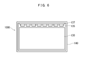
- FIG. 6 shows a configuration of an edge light type backlight device 1000.
- the backlight device 1000 illustrated in FIG. 6 includes a light guide plate 130 and a plurality of LED light sources 135 disposed to face one side surface (end surface) of the light guide plate 130.
- the LED light source 135 is mounted on an LED substrate (mounting substrate) 137.
- the LED substrate on which the LED 135 is mounted and the light guide plate 130 are housed in the backlight chassis 140.
- a notch is formed in the light guide plate 130 in order to fix the light guide plate 130 at a predetermined position of the backlight chassis 140.
- the light guide plate 130 can be fixed and positioned by providing a plurality of pins on the backlight chassis 140 and disposing the pins in the notches.
- FIG. 7A and 7B show a configuration in which the notch 132 is formed in the light guide plate 130.
- FIG. FIG. 7A is a partially enlarged view showing a state in which the notch 132 is formed on the long side of the light guide plate 130.
- the LED element 135 mounted on the LED substrate 137 is disposed to face one side surface of the light guide plate 130.
- FIG. 7B is a partially enlarged view showing a state in which the notch 132 is formed on the short side of the light guide plate 130.
- the notch unevenness occurs due to the influence of the notch portion 132 and the pin 144 located therein. That is, a part of the emitted light from the LED light source 135 is blocked by the pin 144 in the notch 132, and as a result, a bright part and a dark part are generated in the region 155a close to the notch 132, As a result, luminance unevenness (notch unevenness) occurs.
- the present invention has been made in view of such a point, and a main object thereof is to provide a backlight device capable of suppressing the influence of luminance unevenness caused by a notch.
- the present invention provides a backlight device having the following configuration. That is, the backlight device of the present invention is a backlight device that irradiates light onto a liquid crystal display panel, and positions the light source, a light guide plate that irradiates the liquid crystal display panel with light emitted from the light source, and the light guide plate. It has a pin to do.
- the light guide plate has a notch for housing the pin, and the notch is filled with a filling material having a refractive index higher than that of air so as to cover the pin. ing. According to such a configuration, the notch formed in the light guide plate is filled with the filling material having a refractive index higher than that of air so as to cover the pin.
- the difference between the refractive index of the light guide plate and the refractive index inside the notch (filling material) can be reduced as compared with the conventional configuration in which the periphery of the pin in the notch is covered with air. it can. As a result, it is possible to suppress luminance unevenness (notch unevenness) caused by the notch portion in which the pin is accommodated.
- the filling material is a gel polystyrene resin or a gel silicone resin.
- the filling material is a viscous material.
- the refractive index of the filling material is substantially the same as the refractive index of the material constituting the light guide plate.
- the light guide plate has a rectangular shape having four sides, and the cutout portion is formed at least one on each of the four sides.
- the light guide plate has a rectangular shape having four sides, and the light source is disposed to face one side of the four sides of the rectangular shape.
- the notch portion is formed on a side of the four sides excluding one side on which the light source is opposed.
- the backlight device further includes a chassis that houses the light guide plate, the pins are disposed in the chassis, and the light source is a light emitting diode element.
- a liquid crystal display device is a liquid crystal display device including the backlight device.
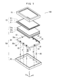
- FIG. 5 is an exploded view for explaining a correspondence relationship between a notch portion 32 and a pin 44 of the light guide plate 30.
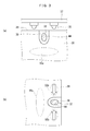
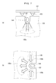
- (A) And (b) is a top view for demonstrating the mode of the periphery of the notch part 32 of the light-guide plate 30 which concerns on embodiment of this invention. It is an exploded view explaining the modification of the light-guide plate 30 which concerns on embodiment of this invention.
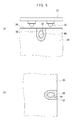
- (A) And (b) is a top view for demonstrating the mode of the periphery of the notch part 32 of the modification of the light-guide plate 30 which concerns on embodiment of this invention. It is a top view which shows the structure of the backlight apparatus 1000 typically.
- (A) And (b) is a partial enlarged plan view for demonstrating the subject in the backlight apparatus 1000.
- an active matrix type (TFT type) liquid crystal display device 100 including a liquid crystal display panel 10 as an example.
- symbol is attached
- the dimensional relationship (length, width, thickness, etc.) in each drawing does not necessarily accurately reflect the actual dimensional relationship.
- “front side” or “front side” means a side facing the viewer (viewer) in the liquid crystal display device 100 (that is, the liquid crystal display panel 10 side), and “back side” or “back side”. Means the side of the liquid crystal display device 100 that does not face the viewer (that is, the backlight device 50 side).
- the liquid crystal display device 100 includes a liquid crystal display panel 10 and a backlight device 50 that is an external light source disposed on the back side of the liquid crystal display panel 10.
- the liquid crystal display panel 10 and the backlight device 50 are integrally held by being assembled by a bezel (frame body) 70 or the like.
- the liquid crystal display panel 10 generally has a rectangular shape as a whole, and is a display area (not shown) that is an area in which a pixel is formed at the center and displays an image. have.
- the liquid crystal display panel 10 of the present embodiment has a size of, for example, 20 inches to 110 inches (typically 32 inches to 60 inches), but is not limited to these sizes. .
- the liquid crystal display panel 10 has a sandwich structure composed of a pair of transparent glass substrates 11 and 12 facing each other and a liquid crystal layer sealed therebetween.
- the front side is the color filter substrate (CF substrate) 12
- the back side is the array substrate 11.
- a sealing material (not shown) is provided on the periphery of the CF substrate 12 and the array substrate 11 so as to surround the periphery of the display area described above, and seals the liquid crystal layer.
- the liquid crystal layer is composed of a liquid crystal material containing liquid crystal molecules.
- the alignment of liquid crystal molecules is manipulated with the application of an electric field between the array substrate 11 and the CF substrate 12, and the optical characteristics change.
- An alignment film (not shown) for determining the alignment direction of the liquid crystal molecules is formed on the opposite surfaces (inner side) of the substrates 11 and 12, respectively.
- the polarizing plate 13 is affixed to each.
- the backlight device 50 of this embodiment disposed on the back side (back side) of the liquid crystal display panel 10 is a light source unit that irradiates the liquid crystal display panel 10 with light.
- the backlight device 50 of the example shown in FIG. 1 is an edge light type backlight unit, and specifically, converts a light source (a plurality of light emitting elements) 35 and light emitted from the light source 35 into planar light. And a light guide plate 30 that irradiates the liquid crystal display panel 10.
- the light source (light emitting element) 35 of this embodiment is an LED element (point light source).
- a plurality of LED elements 35 are mounted on a wiring board (LED board) 37.
- the light emitting element 35 is disposed to face one of the side surfaces (incident surface) 36 of the light guide plate 30, and the light emitted from the light emitting element 35 enters the light guide plate 30 from the incident surface 36 of the light guide plate 30.
- the light emitting element 35 was arrange
- the light emitting element 35 may be disposed in the vicinity of a surface facing it and / or a surface orthogonal thereto.
- the light guide plate 30 is formed by injection molding or the like into a rectangular flat plate having a size that covers the display area of the liquid crystal display panel 10, and the light incident on the incident surface 36 is planar from the light emitting surface (main surface) 30 a. Is an optical member that irradiates the light.
- the material which comprises the light-guide plate 30 will not be restrict
- a dot pattern (not shown) is formed on the bottom surface 30 c of the light guide plate 30 to scatter light and increase the light use efficiency. Such a dot pattern is formed by printing using an ink or the like that forms a reflection pattern or a diffusion pattern.
- a notch 32 for positioning the light guide plate 30 is formed.
- the illustrated light guide plate 30 has a rectangular shape having four sides, and in the illustrated example, at least one notch 32 is formed on each of the four sides.
- the rectangular shape of the light guide plate 30 is not limited to a geometrical rectangle, and includes a case where the corners are rounded and the short side and the long side are not exactly right angles. Including the shape).
- the illustrated notch 32 is provided at three locations on the long side and one location on the short side of the light guide plate 30, but is not limited thereto, and is suitably suitable depending on the dimensions and positioning accuracy conditions of the light guide plate 30. Should be adopted.
- the cutout portion 32 of the present embodiment is a concave portion (groove portion) having a substantially U-shape, and is produced by cutting out the light guide plate 30.
- the notch 32 is not limited to a U-shape, and may be a rectangular shape.
- a pin 44 is disposed in the notch 32, and the light guide plate 30 is positioned and fixed by the pin 44.
- the light guide plate 30 is formed with a notch 32 for accommodating the pin 44, and the light guide plate 30 is fixed by a combination of the notch 32 and the pin 44.
- the correspondence between the notch 32 and the pin 44 is as shown in FIG.
- the pin 44 of the present embodiment is not limited in material and the like as long as it has a strength capable of positioning the light guide plate 30, but is made of metal (for example, aluminum, stainless steel, iron, etc.), resin, or the like. It is configured.
- the pin 44 is displayed so that the correspondence with the notch 32 can be understood.
- the pin 44 accommodates the light guide plate 30.
- the chassis (backlight chassis) 40 is arranged.
- the cross-sectional shape of the pin 44 is an oval shape or a substantially oval shape corresponding to the U-shaped notch 32, but is not limited thereto.
- the cross-sectional shape of the pin 44 can be circular or polygonal (for example, regular hexagon, regular octagon, etc.).
- the pin 44 of the present embodiment is fixed to the bottom surface of the chassis 40 so as to penetrate through the notch 32 of the light guide plate 30.
- the chassis 40 according to the present embodiment includes a rectangular (typically rectangular) bottom surface portion and a frame-shaped side wall portion formed so as to surround the bottom surface portion. It has an open box shape.
- the chassis 40 is made of a metal material (for example, aluminum, iron, etc.) and is a sheet metal member that covers the entire back surface of the liquid crystal display device 100.
- a reflective sheet (not shown) may be disposed between the chassis 40 and the light guide plate 30.
- a plurality of sheet-like optical sheets 21 are stacked on the front side of the light guide plate 30 to cover the opening of the chassis 40.
- the optical sheet 21 for example, a lens sheet 21a, a prism sheet 21b, and a diffusion plate 21c are sequentially arranged from the liquid crystal display panel 10 side toward the chassis 40 side.
- the combination and order are not limited thereto.
- the notch 32 of the light guide plate 30 is filled with the filling material 38.
- the filling material 38 is made of a material having a refractive index higher than that of air. Moreover, the filling material 38 is filled in the notch 32 so as to cover the pin.
- 3 (a) and 3 (b) are partial enlarged views showing the periphery of the notch 32 formed on the long side and the short side of the light guide plate 30 of the present embodiment, respectively.
- FIG. 3A the LED element 35 disposed to face one side 36 of the light guide plate 30 is shown.
- the notch 32 is filled with a filling material 38 so as to cover the pins 44.
- a filling material 38 of the present embodiment is a gel polystyrene resin, a gel silicone resin, or the like.
- a gel-like polystyrene resin is used as the filling material 38.
- an ultraviolet curable resin is used as the filling material 38, the resin filled in the notch 32 is cured by irradiating ultraviolet rays, which is convenient.
- the refractive index of the filling material 38 in this example is, for example, 1.33 or more, and is preferably substantially the same as the refractive index of the material constituting the light guide plate 30 (around 1.5).
- the filling material 38 is disposed so as to cover the pin 44 in the notch 32, compared with the configuration in which the periphery of the pin 44 in the notch 32 is air. Further, the influence of luminance unevenness due to the notch 32 and the pin 44 can be suppressed. That is, since the inside of the notch 32 of this embodiment is filled with the filling material 38 having a refractive index larger than the refractive index of air, reflection at the interface of the notch 32 can be suppressed. Therefore, compared with the luminance unevenness (notch unevenness) in the region 155a in the configuration shown in FIG. 7A, the luminance unevenness in the region 55a close to the notch 32 shown in FIG. Cutout unevenness) can be greatly reduced. If the refractive index of the filling material 38 is made substantially the same as the refractive index of the light guide plate 30, the problem of uneven brightness can be further solved.
- the problem of uneven brightness can also be solved in the notch 32 shown in FIG. More specifically, even if light (55b) emitted from the LED light source 35 and propagating through the light guide plate 30 hits the side surface (end surface) that defines the notch 32, the notch 32 is filled with the filling material 38. Therefore, total reflection is substantially prevented from occurring at the interface of the notch 32. Therefore, the occurrence of luminance unevenness (light leakage) caused by the collection of light generated in the region 155c in the configuration shown in FIG. 7B can be alleviated in the configuration shown in FIG. 3B. If the refractive index of the filling material 38 is substantially the same as the refractive index of the light guide plate 30, the problem of uneven brightness (light leakage) can be further solved.
- the notch 32 is formed on any of the four sides of the light guide plate 30, but is not limited thereto.
- the notch 32 is not provided on the side that becomes the incident surface 36 facing the LED element 35, but the notch 32 is provided on any or all of the remaining three sides. It doesn't matter. In particular, in the vicinity of a portion where the emitted light of the LED element 35 is incident, there is a high possibility that luminance unevenness (notch unevenness) occurs. Therefore, if the light guide plate 30 can be appropriately positioned, its side (incident surface) It may be one of the preferable configurations that the notch portion 32 is not formed in 36).
- the filling material 39 is a viscous material.
- 5A and 5B correspond to FIGS. 3A and 3B.
- the notch 32 is filled with the filling material 39 having viscosity, in addition to the effect of suppressing the luminance unevenness, the holding force between the light guide plate 30 and the chassis 40 can be improved. As a result, vibration and / or It is possible to construct a backlight device 50 that is resistant to falling.
- the structure in which the filling material 38 (39) is filled in the notch 32 that penetrates the pin 44 for positioning the light guide plate 30 has been described.
- a technique of disposing an LED element in a recess-shaped notch in a light guide plate for example, Patent Document 2.
- an LED element is arranged in a recess-shaped notch and is fixed with an adhesive, and the periphery of the pin 44 in the notch 32 according to the embodiment of the present invention is covered with a filler.
- the LED element 35 is not disposed in the notch 32 in the configuration of the embodiment of the present invention. If the LED element is arranged in the notch and fixed with an adhesive, a design margin cannot be provided between the light guide plate and the LED element. As a result, due to thermal expansion of the light guide plate, etc. There is a possibility that the LED element is damaged.
- the LED element 35 is used as the light source (light emitting element).
- the light source 35 is not disposed in the notch 32 and the pin 44 is disposed in the notch 32. If it is the structure which is made, other things (for example, cold cathode fluorescent tube (CCFL)) may be used as a light source.
- the problem of uneven brightness can be alleviated by the filler 38 (39) having a high refractive index located around the pin 44.
- the filler 38 (39) having a high refractive index located around the pin 44.
- a part of the pin 44 comes into contact with the wall surface of the notch 32 due to the alignment tolerance, and the other region is filled with the filling material 38 (39). )
- the effect of eliminating luminance unevenness can be obtained as compared with the conventional configuration in which the notch 32 is covered with air.
- the present invention it is possible to provide a backlight device that can suppress the influence of luminance unevenness caused by the notch.
Landscapes
- Physics & Mathematics (AREA)
- General Physics & Mathematics (AREA)
- Optics & Photonics (AREA)
- Planar Illumination Modules (AREA)
- Liquid Crystal (AREA)
Abstract
切り欠き部によって生じる輝度ムラの影響を抑制することができるバックライト装置を提供する。本発明によって提供される液晶表示パネル10に光を照射するバックライト装置50は、光源35と、光源35が発した光を液晶表示パネル10に照射させる導光板30と、導光板30を位置決めするピン44とを備える。導光板30には、ピン44を収納する切り欠き部32が形成され、切り欠き部32には、ピン44を覆うように、空気の屈折率よりも高い屈折率を有する充填材料38が充填されている。
Description
本発明は、液晶表示パネルを照射する光源を備えたバックライト装置および該バックライト装置を備える液晶表示装置に関し、より詳しくは、導光板を備えるエッジライト型のバックライト装置に関する。
なお、本出願は2011年6月21日に出願された日本国特許出願2011-137407号に基づく優先権を主張しており、その出願の全内容は本明細書中に参照として組み入れられている。
なお、本出願は2011年6月21日に出願された日本国特許出願2011-137407号に基づく優先権を主張しており、その出願の全内容は本明細書中に参照として組み入れられている。
近年、テレビ、パソコン等の画像表示装置(ディスプレイ)として用いられている液晶表示装置の薄型化が進んでいる。かかる薄型化を実現するべく、例えば、液晶表示パネルの背面側に導光板を配置して、導光板の端部(即ち液晶表示パネルの縁)に光源(例えば発光ダイオード素子)を配置するエッジライト型のバックライト装置が採用されている(例えば、特許文献1など)。
図6は、エッジライト型のバックライト装置1000の構成を示している。図6に示したバックライト装置1000は、導光板130と、導光板130の一側面(端面)に対向して配置される複数のLED光源135とから構成されている。LED光源135は、LED基板(実装基板)137に実装されている。そして、LED135が実装されたLED基板および導光板130は、バックライトシャーシ140に収納されている。
図6に示したバックライト装置1000では、導光板130をバックライトシャーシ140の所定位置に固定するために、導光板130に切り欠きが形成される。そして、バックライトシャーシ140にピンを複数本設けて、そのピンを切り欠き内に配置することによって導光板130を固定して位置決めすることができる。
図7(a)および(b)は、導光板130に切り欠き部132が形成された構成を示している。図7(a)では、導光板130の長辺側に切り欠き部132が形成された様子を示す部分拡大図である。図7(a)では、導光板130の一側面に対向して、LED基板137に実装されたLED素子135が配置されている。また、図7(b)では、導光板130の短辺側に切り欠き部132が形成された様子を示す部分拡大図である。
本願発明者が、導光板130の切り欠き部132による影響を検討した結果、次のようなことがわかった。
まず、図7(a)に示すように、LED光源135が近接している切り欠き部132では、切り欠き部132およびその中に位置するピン144の影響によって、切り欠きムラが生じてしまう。すなわち、LED光源135からの出射光の一部が、切り欠き部132内のピン144によって遮られて、その結果、切り欠き部132に近接した領域155aにおいて、明るい部分と暗い部分が発生し、それによって、輝度ムラ(切り欠きムラ)が生じる。
さらに、図7(b)に示すように、導光板130の短辺側に形成された切り欠き部132においても輝度ムラが生じる可能性がある。LED光源135から出射されて導光板130内を伝播する光(155b)が、切り欠き部132を規定する側面(端面)で全反射すると、切り欠き部132に近接した領域155cに光が集まってしまい(光漏れ)、それによって、輝度ムラ(切り欠きムラ)が生じる。
本発明はかかる点に鑑みてなされたものであり、その主な目的は、切り欠き部によって生じる輝度ムラの影響を抑制することができるバックライト装置を提供することにある。
上記目的を実現するべく、本発明により、以下の構成のバックライト装置が提供される。即ち、本発明のバックライト装置は、液晶表示パネルに光を照射するバックライト装置であり、光源と、前記光源が発した光を前記液晶表示パネルに照射させる導光板と、前記導光板を位置決めするピンとを備えている。前記導光板には、前記ピンを収納する切り欠き部が形成されており、前記切り欠き部には、前記ピンを覆うように、空気の屈折率よりも高い屈折率を有する充填材料が充填されている。
かかる構成によると、導光板に形成された切り欠き部において、ピンを覆うように、空気よりも高い屈折率を有する充填材料が充填されている。したがって、切り欠き部内におけるピンの周囲が空気で覆われていた従来の構成と比較して、導光板の屈折率と切り欠き部の内部(充填材料)の屈折率との差を小さくすることができる。その結果、ピンが収納された切り欠き部に起因して生じる輝度ムラ(切り欠きムラ)を抑制することが可能となる。
かかる構成によると、導光板に形成された切り欠き部において、ピンを覆うように、空気よりも高い屈折率を有する充填材料が充填されている。したがって、切り欠き部内におけるピンの周囲が空気で覆われていた従来の構成と比較して、導光板の屈折率と切り欠き部の内部(充填材料)の屈折率との差を小さくすることができる。その結果、ピンが収納された切り欠き部に起因して生じる輝度ムラ(切り欠きムラ)を抑制することが可能となる。
ここで開示されるバックライト装置の好適な一態様では、前記充填材料は、ゲル状ポリスチレン樹脂またはゲル状シリコーン樹脂である。
ここで開示されるバックライト装置の好適な一態様では、前記充填材料は、粘性を有する材料である。
ここで開示されるバックライト装置の好適な一態様では、前記充填材料の屈折率は、前記導光板を構成する材料の屈折率と略同一である。
ここで開示されるバックライト装置の好適な一態様では、前記導光板は、四辺を有する矩形形状を有しており、前記切り欠き部は、四辺のそれぞれに少なくとも一つずつ形成されている。
ここで開示されるバックライト装置の好適な一態様では、前記導光板は、四辺を有する矩形形状を有しており、前記光源は、前記矩形形状の四辺のうちの一辺に対向して配置されており、前記切り欠き部は、前記四辺のうち、前記光源が対向して配置される一辺を除く辺に形成されている。
ここで開示されるバックライト装置の好適な一態様では、さらに、前記導光板を収納するシャーシを備え、前記ピンは、前記シャーシに配置されており、前記光源は、発光ダイオード素子である。
本発明に係る液晶表示装置は、上記バックライト装置を備えている液晶表示装置である。
以下、図面を参照しながら、本発明の好適な実施形態を説明する。なお、本明細書において特に言及している事項以外の事柄であって本発明の実施に必要な事柄(例えば、液晶表示パネルの構成や構築方法、表示装置に装備される光源の構成等)は、当該分野における従来技術に基づく当業者の設計事項として把握され得る。本発明は、本明細書及び図面によって開示されている内容と当該分野における技術常識とに基づいて実施することができる。
以下、図1から図3を参照しながら、本発明の好ましい一実施形態について、液晶表示パネル10を備えたアクティブマトリックス方式(TFT型)の液晶表示装置100を例に挙げて説明する。
なお、以下の図面において、同じ作用を奏する部材、部位には同じ符号を付し、重複する説明は省略又は簡略化することがある。また、各図における寸法関係(長さ、幅、厚さ等)は、必ずしも実際の寸法関係を正確に反映するものではない。また、以下の説明において、「前面」又は「表側」とは液晶表示装置100における観視者(視聴者)に面する側(すなわち液晶表示パネル10側)をいい、「背面」又は「裏側」とは液晶表示装置100における観視者に面しない側(すなわちバックライト装置50側)を言うこととする。
まず、液晶表示装置100の全体構成について説明する。図1に示すように、液晶表示装置100は、液晶表示パネル10と該液晶表示パネル10の背面側に配置された外部光源であるバックライト装置50とを備えている。液晶表示パネル10とバックライト装置50とは、ベゼル(枠体)70等により組み付けられることで一体的に保持されている。
図1に示すように、液晶表示パネル10は、概して、全体として矩形の形状を有しており、その中央に画素が形成されている領域であって画像を表示する表示領域(図示せず)を有している。なお、本実施形態の液晶表示パネル10は、例えば、20インチから110インチ(典型的には、32インチから60インチ)のサイズを有しているが、それらのサイズに限定されるものではない。
また、液晶表示パネル10は、互いに対向する一対の透明性のガラス基板11,12と、その間に封入される液晶層とから構成されるサンドイッチ構造を有している。上記一対の基板11,12のうち、表側がカラーフィルタ基板(CF基板)12であり、裏側がアレイ基板11である。かかるCF基板12及びアレイ基板11の周縁部には、上述した表示領域の周囲を囲むようにシール材(図示せず)が設けられており、上記液晶層を封止している。
液晶層は、液晶分子を含む液晶材料から構成される。かかる液晶材料は、アレイ基板11とCF基板12との間の電界印加に伴って液晶分子の配向が操作され光学特性が変化する。両基板11,12における互いに対向する側(内側)の面には、それぞれ液晶分子の配向方向を決定する配向膜(図示せず)が形成されており、対向しない側(外側)の面には、それぞれに偏光板13が貼り付けられている。
次に、上記液晶表示パネル10の背面側(裏側)に配置される本実施形態のバックライト装置50は、液晶表示パネル10に光を照射する光源ユニットである。図1に示した例のバックライト装置50は、エッジライト型のバックライトユニットであり、具体的には、光源(複数の発光素子)35と、光源35が発した光を平面光に変換して液晶表示パネル10に照射させる導光板30とを含んでいる。
本実施形態の光源(発光素子)35は、LED素子(点状光源)であり、図1に示した構成例では、複数のLED素子35が配線基板(LED基板)37の上に載置されている。発光素子35は、導光板30の側面の一つ(入射面)36に対向して配置されており、発光素子35から出射された光は、導光板30の入射面36から導光板30内に入射する。なお、発光素子35は、上記のように導光板30の一つの入射面36の近傍に配置したが、それに限られない。たとえば、図示した導光板30の一つの入射面36に加えて、それに対向する面、及び/または、それに直交する面の近傍に発光素子35を配置してもよい。
導光板30は、液晶表示パネル10の表示領域を覆う大きさの長方形の平板状に射出成形等によって形成されており、入射面36に入射した光を、発光面(主面)30aから面状に照射する光学部材である。導光板30を構成する材料は、透光性を有し成形性に優れる材料であれば特に制限されない。例えば、アクリル樹脂、ポリカーボネート樹脂等が挙げられる。導光板30の底面30cには、光を散乱させて光の利用効率を高めるドットパターン(図示せず)が形成されている。かかるドットパターンは、反射パターン又は拡散パターンを形成するインクなどを用いて印刷によって形成されている。
本実施形態の導光板30には、導光板30を位置決めするための切り欠き部32が形成されている。図示した導光板30は、四辺を有する矩形形状を有しており、図示した例では、切り欠き部32は、四辺のそれぞれに少なくとも一つずつ形成されている。導光板30の矩形形状は、幾何学的な長方形に限らず、角が丸くなっていたり、短辺と長辺が厳密に直角でないものも含まれ、その意味においては、実質的に長方形(正方形を含む)の形状であればよい。
図示した切り欠き部32は、導光板30の長辺に3箇所、短辺に1箇所設けられているが、それに限るものではなく、導光板30の寸法・位置決め精度条件などによって適宜好適なものを採用したらよい。本実施形態の切り欠き部32は、略U字型の形状を有する凹部(溝部)であり、導光板30を切り欠き加工することによって作製されている。なお、切り欠き部32は、U字型の形状に限らず、矩形の形状であっても構わない。
本実施形態の構成では、切り欠き部32内にはピン44が配置され、そのピン44によって導光板30は位置決めされて固定されている。言い換えると、導光板30には、ピン44を収納する切り欠き部32が形成されており、切り欠き部32とピン44との組み合わせによって導光板30は固定されている。切り欠き部32とピン44との対応関係は、図2に示す通りである。また、本実施形態のピン44は、導光板30を位置決めすることができる強度を有していれば、材料などに制限はないが、金属(例えば、アルミニウム、ステンレス、鉄など)、樹脂などから構成されている。
なお、図1に示した分解斜視図では、ピン44は、切り欠き部32との対応関係がわかるように表示されているが、本実施形態の構成では、ピン44は、導光板30を収納するシャーシ(バックライトシャーシ)40に配置されている。図示した例では、ピン44の断面形状は、U字型の切り欠き部32に対応させて、長円形状または略楕円形状にしているが、これに限らない。例えば、ピン44の断面形状を円形にすることも可能であるし、多角形形状(例えば、正六角形、正八角形など)にしても構わない。
本実施形態のピン44は、導光板30の切り欠き部32内を貫通するようにシャーシ40の底面に固定されている。本実施形態のシャーシ40は、方形状(典型的には長方形状)の底面部と、該底面部を囲うように形成された枠状の側壁部とから構成されており、前面側に向けて開口した箱型形状をしている。また、シャーシ40は、金属材料(例えば、アルミニウム、鉄など)から構成されており、液晶表示装置100の裏面全体を覆う板金部材である。なお、シャーシ40と導光板30との間には、反射シート(図示せず)を配置してもよい。
図1に示した例では、本実施形態のバックライト装置50には、導光板30の表側に、複数のシート状の光学シート21(21aから21c)が積層されてシャーシ40の開口部を覆うように配置されている。光学シート21の構成としては、例えば、液晶表示パネル10側からシャーシ40側に向かって順に、レンズシート21a、プリズムシート21b、拡散板21cで構成されているが、この組合せおよび順序に限定されない。
本実施形態のバックライト装置50においては、導光板30の切り欠き部32に充填材料38が充填されている。充填材料38は、空気の屈折率よりも高い屈折率を有する材料から構成されている。また、充填材料38は、ピンを覆うように切り欠き部32内に充填されている。
図3(a)および(b)は、それぞれ、本実施形態の導光板30の長辺側および短辺側に形成された切り欠き部32の周囲を示す部分拡大図である。図3(a)では、導光板30の一側面36に対向して配置されたLED素子35を示している。
本実施形態の構成では、切り欠き部32には、ピン44を覆うように充填材料38が充填されている。本実施形態の充填材料38の一例は、ゲル状ポリスチレン樹脂、ゲル状シリコーン樹脂などである。この例では、充填材料38として、ゲル状ポリスチレン樹脂を使用している。また、充填材料38として、紫外線硬化樹脂を用いると、紫外線を照射することによって、切り欠き部32に充填した樹脂の硬化を実行するので便利である。
この例の充填材料38の屈折率は、例えば1.33以上であり、さらには、導光板30を構成する材料の屈折率(1.5付近)と略同一であることが好ましい。
本実施形態の構成によれば、切り欠き部32においてピン44を覆うように充填材料38が配置されているので、切り欠き部32内のピン44の周囲が空気であった構成と比較して、切り欠き部32およびピン44による輝度ムラの影響を抑制することができる。すなわち、本実施形態の切り欠き部32内は、空気の屈折率よりも大きい屈折率を有する充填材料38で埋め尽くしているので、切り欠き部32の界面での反射などを抑えることができる。したがって、図7(a)に示した構成における領域155aでの輝度ムラ(切り欠きムラ)と比較して、図3(a)に示した切り欠き部32に近接した領域55aでの輝度ムラ(切り欠きムラ)は大幅に緩和することができる。そして、充填材料38の屈折率を、導光板30の屈折率と略同一にすると、より一層、輝度ムラの問題を解消することができる。
加えて、図3(b)に示した切り欠き部32においても、輝度ムラの問題を解消することができる。さらに説明すると、LED光源35から出射されて導光板30内を伝播する光(55b)が、切り欠き部32を規定する側面(端面)に当たっても、切り欠き部32内は充填材料38で埋められているので、切り欠き部32の界面で全反射が起こることが実質的に防止される。したがって、図7(b)に示した構成における領域155cに生じた光が集まって生じる輝度ムラ(光漏れ)が生じることを、図3(b)に示した構成では緩和することができる。そして、充填材料38の屈折率を、導光板30の屈折率と略同一にすると、より一層、その輝度ムラ(光漏れ)の問題を解消することができる。
なお、上述した実施形態では、切り欠き部32を、導光板30の四辺のいずれにも形成したが、それに限定されるものではない。例えば、図4に示すように、LED素子35が対向する入射面36となる辺には切り欠き部32は設けずに、残りの3辺のいずれか又は全てに切り欠き部32を設けるようにしても構わない。特に、LED素子35の出射光が入射する部位の近くでは、輝度ムラ(切り欠きムラ)が発生する可能性が高くなるので、導光板30を適切に位置決めできるのであれば、その辺(入射面36)には切り欠き部32を形成しないことも好適な構成の一つであり得る。
また、図5(a)および(b)に示した例では、充填材料39は、粘性を有する材料である。なお、図5(a)および(b)は、図3(a)および(b)に対応した図である。粘性を有する充填材料39で切り欠き部32を充填した場合、輝度ムラを抑制できる効果に加えて、導光板30とシャーシ40との保持力を向上させることができ、その結果、振動および/または落下に強いバックライト装置50を構築することが可能である。
なお、本発明の実施形態のバックライト装置50では、導光板30を位置決めするピン44を貫通させる切り欠き部32内に充填材料38(39)を充填させた構造を説明したが、これとは技術的思想は本質的に異なるものの、導光板の凹部状の切欠部にLED素子を配置する技術がある(例えば、特許文献2)。この技術は、凹部状の切欠部にLED素子を配置してそれを接着剤で固定するものであり、本発明の実施形態に係る切り欠き部32内におけるピン44の周囲を充填材で覆うものとは顕著に異なる。すなわち、本発明の実施形態の構成では切り欠き部32内にLED素子35は配置されていない。なお、LED素子を切り欠き部内に配置して接着剤で固定したとすれば、導光板とLED素子との間に設計マージンを持たせることができなくなり、その結果、導光板の熱膨張などによってLED素子の破損が生じる可能性がでてくる。
また、上記の実施形態では、光源(発光素子)としてLED素子35を使用した例を示したが、切り欠き部32内に光源35が配置されずに、切り欠き部32内にピン44が配置される構成であれば、光源としては、他のもの(例えば、冷陰極蛍光管(CCFL))を使用しても構わない。その場合でも、ピン44の周囲の位置する屈折率の高い充填材38(39)によって、輝度ムラの問題を緩和させることができる。さらに、ピン44の周囲を完全に充填材料38(39)で覆う他、位置合わせの公差によってピン44の一部が切り欠き部32の壁面に接触し、それ以外の領域を充填材料38(39)で覆う場合でも、従来の切り欠き部32内が空気で覆われていた構成と比較すれば、輝度ムラの解消の効果が得られるものである。
以上、本発明の具体例について図面を参照しつつ詳細に説明したが、これらは例示にすぎず、特許請求の範囲を限定するものではない。特許請求の範囲に記載の技術には、以上に例示した具体例を様々に変形、変更したものが含まれる。
本発明によると、切り欠き部によって生じる輝度ムラの影響を抑制することができるバックライト装置を提供することができる。
10 液晶表示パネル
11 アレイ基板
12 カラーフィルタ基板
13 偏光板
21 光学シート
30 導光板
32 切り欠き部
35 光源(LED素子)
36 入射面
38 充填材料
39 充填材料
40 シャーシ
44 ピン
50 バックライト装置
100 液晶表示装置
11 アレイ基板
12 カラーフィルタ基板
13 偏光板
21 光学シート
30 導光板
32 切り欠き部
35 光源(LED素子)
36 入射面
38 充填材料
39 充填材料
40 シャーシ
44 ピン
50 バックライト装置
100 液晶表示装置
Claims (8)
- 液晶表示パネルに光を照射するバックライト装置であって、
光源と、
前記光源が発した光を前記液晶表示パネルに照射させる導光板と、
前記導光板を位置決めするピンと
を備え、
前記導光板には、前記ピンを収納する切り欠き部が形成されており、
前記切り欠き部には、前記ピンを覆うように、空気の屈折率よりも高い屈折率を有する充填材料が充填されていることを特徴とする、バックライト装置。 - 前記充填材料は、ゲル状ポリスチレン樹脂またはゲル状シリコーン樹脂である、請求項1に記載のバックライト装置。
- 前記充填材料は、粘性を有する材料である、請求項1に記載のバックライト装置。
- 前記充填材料の屈折率は、前記導光板を構成する材料の屈折率と略同一である、請求項1から3のいずれか一項に記載のバックライト装置。
- 前記導光板は、四辺を有する矩形形状を有しており、
前記切り欠き部は、四辺のそれぞれに少なくとも一つずつ形成されている、請求項1から4のいずれか一項に記載のバックライト装置。 - 前記導光板は、四辺を有する矩形形状を有しており、
前記光源は、前記矩形形状の四辺のうちの一辺に対向して配置されており、
前記切り欠き部は、前記四辺のうち、前記光源が対向して配置される一辺を除く辺に形成されている、請求項1から4のいずれか一項に記載のバックライト装置。 - さらに、前記導光板を収納するシャーシを備え、
前記ピンは、前記シャーシに配置されており、
前記光源は、発光ダイオード素子である、請求項1から6のいずれか一項に記載のバックライト装置。 - 請求項1から7のいずれか一項に記載のバックライト装置を備えていることを特徴とする、液晶表示装置。
Applications Claiming Priority (2)
| Application Number | Priority Date | Filing Date | Title |
|---|---|---|---|
| JP2011-137407 | 2011-06-21 | ||
| JP2011137407 | 2011-06-21 |
Publications (1)
| Publication Number | Publication Date |
|---|---|
| WO2012176676A1 true WO2012176676A1 (ja) | 2012-12-27 |
Family
ID=47422516
Family Applications (1)
| Application Number | Title | Priority Date | Filing Date |
|---|---|---|---|
| PCT/JP2012/065188 Ceased WO2012176676A1 (ja) | 2011-06-21 | 2012-06-14 | バックライト装置および該バックライト装置を備える液晶表示装置 |
Country Status (1)
| Country | Link |
|---|---|
| WO (1) | WO2012176676A1 (ja) |
Cited By (2)
| Publication number | Priority date | Publication date | Assignee | Title |
|---|---|---|---|---|
| CN108490530A (zh) * | 2018-03-26 | 2018-09-04 | 京东方科技集团股份有限公司 | 一种超窄边框模组及一种液晶显示装置 |
| US11022257B2 (en) | 2019-04-23 | 2021-06-01 | Lumileds Llc | LED light engine features |
Citations (3)
| Publication number | Priority date | Publication date | Assignee | Title |
|---|---|---|---|---|
| JP2004029778A (ja) * | 1993-10-27 | 2004-01-29 | Seiko Epson Corp | 液晶プロジェクタ |
| JP2010113904A (ja) * | 2008-11-05 | 2010-05-20 | Fujikura Ltd | 面状発光装置、電子機器、及び面状発光装置の製造方法 |
| JP2010192280A (ja) * | 2009-02-19 | 2010-09-02 | Panasonic Corp | 導光シート及びこれを用いた可動接点体 |
-
2012
- 2012-06-14 WO PCT/JP2012/065188 patent/WO2012176676A1/ja not_active Ceased
Patent Citations (3)
| Publication number | Priority date | Publication date | Assignee | Title |
|---|---|---|---|---|
| JP2004029778A (ja) * | 1993-10-27 | 2004-01-29 | Seiko Epson Corp | 液晶プロジェクタ |
| JP2010113904A (ja) * | 2008-11-05 | 2010-05-20 | Fujikura Ltd | 面状発光装置、電子機器、及び面状発光装置の製造方法 |
| JP2010192280A (ja) * | 2009-02-19 | 2010-09-02 | Panasonic Corp | 導光シート及びこれを用いた可動接点体 |
Cited By (5)
| Publication number | Priority date | Publication date | Assignee | Title |
|---|---|---|---|---|
| CN108490530A (zh) * | 2018-03-26 | 2018-09-04 | 京东方科技集团股份有限公司 | 一种超窄边框模组及一种液晶显示装置 |
| US11022257B2 (en) | 2019-04-23 | 2021-06-01 | Lumileds Llc | LED light engine features |
| US11073251B2 (en) | 2019-04-23 | 2021-07-27 | Lumileds Llc | Flexible printed wiring structure for LED light engine |
| US11209131B2 (en) | 2019-04-23 | 2021-12-28 | Lumileds Llc | Alignment features for LED light engine |
| TWI843844B (zh) * | 2019-04-23 | 2024-06-01 | 荷蘭商露明控股公司 | Led光引擎組裝之方法 |
Similar Documents
| Publication | Publication Date | Title |
|---|---|---|
| CN102022673B (zh) | 背光单元和具有该背光单元的液晶显示设备 | |
| US20160161664A1 (en) | Display apparatus | |
| EP2696234A1 (en) | Backlight device | |
| CN106104141B (zh) | 照明装置和显示装置 | |
| CN110058452B (zh) | 照明装置和显示装置 | |
| KR20120076071A (ko) | 액정 표시 장치 | |
| WO2014157482A1 (ja) | 照明装置及び表示装置 | |
| JP2013008016A (ja) | 表示装置 | |
| KR20090042452A (ko) | 액정 표시장치 | |
| WO2014073348A1 (ja) | 表示装置 | |
| WO2018051855A1 (ja) | 光学部材、照明装置及び表示装置 | |
| WO2014010523A1 (ja) | 光学部材、照明装置、及び表示装置 | |
| KR20110088811A (ko) | 백라이트 어셈블리 및 그를 포함하는 표시 장치 | |
| JP5032677B2 (ja) | 液晶モジュール及び液晶表示装置 | |
| JP5604342B2 (ja) | 額縁被覆部材 | |
| KR20130075369A (ko) | 액정표시장치모듈 | |
| JP6160204B2 (ja) | 表示装置および電子装置 | |
| KR101922062B1 (ko) | 액정표시장치 및 그 제조방법 | |
| KR101824603B1 (ko) | 백라이트 유닛 및 이를 구비한 액정표시장치 | |
| KR101472140B1 (ko) | 액정표시장치 | |
| CN105992623A (zh) | 显示装置以及显示装置的制造方法 | |
| JP5051158B2 (ja) | 保護板一体型表示装置 | |
| KR101737799B1 (ko) | 차광테이프와 이를 적용한 백라이트 유닛 및 이를 구비한 액정표시장치 | |
| KR20120025900A (ko) | 에지형 백라이트 유닛 및 이를 이용한 액정표시장치 | |
| WO2012176676A1 (ja) | バックライト装置および該バックライト装置を備える液晶表示装置 |
Legal Events
| Date | Code | Title | Description |
|---|---|---|---|
| 121 | Ep: the epo has been informed by wipo that ep was designated in this application |
Ref document number: 12802423 Country of ref document: EP Kind code of ref document: A1 |
|
| NENP | Non-entry into the national phase |
Ref country code: DE |
|
| 122 | Ep: pct application non-entry in european phase |
Ref document number: 12802423 Country of ref document: EP Kind code of ref document: A1 |
|
| NENP | Non-entry into the national phase |
Ref country code: JP |