WO2012173173A1 - 半導体試料中の金属汚染評価方法および半導体基板の製造方法 - Google Patents
半導体試料中の金属汚染評価方法および半導体基板の製造方法 Download PDFInfo
- Publication number
- WO2012173173A1 WO2012173173A1 PCT/JP2012/065200 JP2012065200W WO2012173173A1 WO 2012173173 A1 WO2012173173 A1 WO 2012173173A1 JP 2012065200 W JP2012065200 W JP 2012065200W WO 2012173173 A1 WO2012173173 A1 WO 2012173173A1
- Authority
- WO
- WIPO (PCT)
- Prior art keywords
- dlts
- spectrum
- metal contamination
- semiconductor
- evaluation
- Prior art date
- Legal status (The legal status is an assumption and is not a legal conclusion. Google has not performed a legal analysis and makes no representation as to the accuracy of the status listed.)
- Ceased
Links
Images






Classifications
-
- H—ELECTRICITY
- H10—SEMICONDUCTOR DEVICES; ELECTRIC SOLID-STATE DEVICES NOT OTHERWISE PROVIDED FOR
- H10P—GENERIC PROCESSES OR APPARATUS FOR THE MANUFACTURE OR TREATMENT OF DEVICES COVERED BY CLASS H10
- H10P74/00—Testing or measuring during manufacture or treatment of wafers, substrates or devices
- H10P74/20—Testing or measuring during manufacture or treatment of wafers, substrates or devices characterised by the properties tested or measured, e.g. structural or electrical properties
- H10P74/203—Structural properties, e.g. testing or measuring thicknesses, line widths, warpage, bond strengths or physical defects
-
- G—PHYSICS
- G01—MEASURING; TESTING
- G01R—MEASURING ELECTRIC VARIABLES; MEASURING MAGNETIC VARIABLES
- G01R31/00—Arrangements for testing electric properties; Arrangements for locating electric faults; Arrangements for electrical testing characterised by what is being tested not provided for elsewhere
- G01R31/26—Testing of individual semiconductor devices
- G01R31/2607—Circuits therefor
- G01R31/2632—Circuits therefor for testing diodes
-
- H—ELECTRICITY
- H10—SEMICONDUCTOR DEVICES; ELECTRIC SOLID-STATE DEVICES NOT OTHERWISE PROVIDED FOR
- H10P—GENERIC PROCESSES OR APPARATUS FOR THE MANUFACTURE OR TREATMENT OF DEVICES COVERED BY CLASS H10
- H10P74/00—Testing or measuring during manufacture or treatment of wafers, substrates or devices
- H10P74/20—Testing or measuring during manufacture or treatment of wafers, substrates or devices characterised by the properties tested or measured, e.g. structural or electrical properties
- H10P74/207—Electrical properties, e.g. testing or measuring of resistance, deep levels or capacitance-voltage characteristics
Definitions
- the present invention relates to a method for evaluating metal contamination in a semiconductor sample, and more particularly to a method for evaluating metal contamination that enables evaluation of a trace amount of metal contamination in a semiconductor sample by a DLTS method (Deep-Level Transient Spectroscopy). It is. Furthermore, the present invention relates to a method for manufacturing a semiconductor substrate that provides a product substrate that is quality-controlled based on the evaluation results obtained by the method.
- DLTS method Deep-Level Transient Spectroscopy
- Metal contamination of the semiconductor substrate adversely affects the device characteristics of the product.
- a heavy metal such as Fe or Ni enters Si, it forms a deep level in the band gap and acts as a carrier capture center or recombination center, which causes pn junction leakage in the device and a decrease in lifetime. Therefore, in order to provide a high-quality semiconductor substrate with little metal contamination, a method for evaluating metal contamination in the semiconductor substrate with high reliability is required.
- V R Reverse voltage
- V 1 Reverse voltage
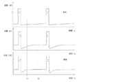
- the transient response of the capacitance (capacitance) of the diode generated corresponding to the voltage is measured (see the lower diagram of FIG. 12).
- the voltage application and the capacity measurement in the above 1) and 2) are performed while sweeping the sample temperature within a predetermined temperature range.
- FIG. 13 is a schematic diagram of temperature dependence.
- the DLTS signal ( ⁇ C) is usually defined as follows.
- ⁇ C C (t1) ⁇ C (t2) (1)
- C (t1) is a capacity at time t1 when a predetermined period has elapsed from the voltage application
- C (t2) is a capacity at time t2 when a predetermined period has elapsed since C (t1) measurement.
- a method of using a lock-in amplifier to obtain a DLTS signal by taking the difference between the integrated values of the first half and the second half of the transient response is often used.
- the DLTS signal ⁇ C is a minute signal
- the measured value ⁇ C is usually taken into a computer and an average value is obtained for each temperature.
- the temperature sweep is linearly performed, and T ⁇ 0.5 to 1 [
- the average value of ⁇ C acquired in the range of K] is ⁇ C at the temperature T [K].
- the reason why a spectrum having a shape as shown in FIG. 14 is obtained is that the speed of carrier emission depends on temperature as follows.
- the deep level concentration (N T ) can be calculated by the following equation (2).
- N T is a dopant concentration
- [Delta] C MAX is the depletion layer capacitance after the release was almost completed carrier from DLTS intensity of the signal
- FIG. 14 shows the result of the Arrhenius plot of the relationship between the peak position (temperature) and e obtained by the measurement of FIG. 14 and collation with a library built in the measuring instrument. From FIG. 15, it can be seen that the DLTS signal detected in FIG. 14 is likely to be due to the Fe—B pair. From this result, the contaminating metal species can be identified as Fe.
- the DLTS signal from the deep level is sufficiently large, and the influence of the baseline tilt and undulation is sufficiently small and negligible. Is easy to detect.
- semiconductor devices such as silicon wafers have been cleaned (reduced metal impurity concentration) with the advancement of the performance of semiconductor devices. Therefore, the DLTS method has been updated to evaluate trace metal contamination. There is a need for higher sensitivity.
- the DLTS signal is extremely weak because the amount of metal impurities that can cause deep levels is small.
- One embodiment of the present invention provides a means for performing metal contamination evaluation of a semiconductor substrate with higher sensitivity by the DLTS method.
- One embodiment of the present invention provides: A method for evaluating metal contamination in a semiconductor sample by a DLTS method, Against the formed semiconductor junction on a semiconductor sample to be evaluated, applied alternately and periodically and weak voltages V 1 for capturing a reverse voltage V R and the carrier to the depletion layer to form a depletion layer
- V 1 for capturing a reverse voltage V R and the carrier to the depletion layer to form a depletion layer
- To measure the DLTS signal generated by changing the temperature to obtain the first DLTS spectrum With respect to the semiconductor junction, to obtain a second DLTS spectra measured while changing the temperature of the DLTS signal generated by applying the V R periodically, Obtaining a difference spectrum between the correction spectrum and the first DLTS spectrum using the second DLTS spectrum or a spectrum obtained by approximating the second DLTS spectrum as a straight line or a curve as a correction spectrum;
- Including The present invention relates to the metal contamination evaluation method for performing metal contamination evaluation in the semiconductor sample using the difference spectrum as
- the metal contamination evaluation may include identifying a contamination metal species based on a peak position of the evaluation DLTS spectrum.
- the correction spectrum may be an approximate curve of the second DLTS spectrum.
- a single temperature sweep is performed.
- a first DLTS spectrum and a second DLTS spectrum can be obtained.
- Another aspect of the present invention provides: Preparing a lot of semiconductor substrates comprising a plurality of semiconductor substrates; Extracting at least one semiconductor substrate from the lot; Evaluating metal contamination of the extracted semiconductor substrate; A semiconductor substrate manufacturing method including a step of shipping, as a product substrate, another semiconductor substrate in the same lot as the semiconductor substrate in which the metal contamination is determined to be an allowable level or less as a result of the evaluation,
- the present invention relates to the manufacturing method, wherein the metal contamination evaluation of the extracted semiconductor substrate is performed by the metal contamination evaluation method.
- the measurement results include baseline tilt and undulation that do not result from the capture and emission of carriers due to deep levels, so the deep level energy level (ET) and the capture cross section for carriers ( ⁇ ) and level density (NT) quantitative error results.
- ET deep level energy level
- ⁇ capture cross section for carriers
- NT level density
- the detection sensitivity for deep levels of the DLTS method is improved. Can be improved.
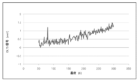
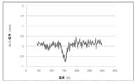
- FIG. 1 is a first DLTS spectrum obtained in Example 1.
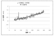
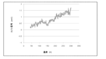
- FIG. 2 is a second DLTS spectrum obtained in Example 1.
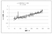
- FIG. 3 shows an approximate straight line obtained by linearly approximating the second DLTS spectrum shown in FIG.
- FIG. 4 shows an approximate curve obtained by approximating the second DLTS spectrum shown in FIG. 2 with a logarithmic function.
- FIG. 5 shows an approximate curve obtained by approximating the second DLTS spectrum shown in FIG. 2 with a cubic polynomial.
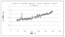
- FIG. 6 shows an approximate curve obtained by approximating the second DLTS spectrum shown in FIG. 2 with a quintic polynomial.
- FIG. 7 shows a result of connecting approximate straight lines obtained by linearly approximating the second DLTS spectrum shown in FIG. FIG.
- FIG. 8 is a difference spectrum between the near-order curve shown in FIG. 6 and the first DLTS spectrum shown in FIG.
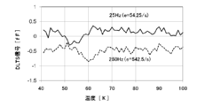
- FIG. 9 is a first DLTS spectrum obtained in Example 2.
- FIG. 10 is a difference spectrum between the first DLTS spectrum shown in FIG. 9 and an approximate curve obtained by approximating the second DLTS spectrum obtained in Example 2 with a quartic polynomial.
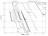
- FIG. 11 shows a deep level library detected by DLTS as an electron trap in n-type silicon.
- FIG. 12 is an explanatory diagram outlining the conventional DLTS method.
- FIG. 13 is an explanatory diagram outlining the conventional DLTS method.
- FIG. 14 is an explanatory diagram outlining the conventional DLTS method.
- FIG. 15 is an explanatory diagram outlining the conventional DLTS method.
- the present invention relates to a method for evaluating metal contamination in a semiconductor sample by a DLTS method (hereinafter also referred to as “the evaluation method of the present invention”).
- the evaluation method of the present invention is: Against the formed semiconductor junction on a semiconductor sample to be evaluated, applied alternately and periodically and weak voltages V 1 for capturing a reverse voltage V R and the carrier to the depletion layer to form a depletion layer To measure the DLTS signal generated by changing the temperature to obtain the first DLTS spectrum, With respect to the semiconductor junction, to obtain a second DLTS spectra measured while changing the temperature of the DLTS signal generated by applying the V R periodically, Obtaining a difference spectrum between the correction spectrum obtained by approximating the second DLTS spectrum by a straight line or a curve and the first DLTS spectrum; Metal contamination in the semiconductor sample is evaluated using the difference spectrum as an evaluation DLTS spectrum.
- a voltage applied so that a current flows in a direction from the p-type to the n-type with respect to the semiconductor junction is referred to as a forward voltage, and a voltage applied in the opposite direction is a reverse voltage.
- a reverse voltage As is well known in the art, when a reverse voltage is applied, no current flows through the semiconductor junction, so that a depletion layer is formed in the semiconductor junction.
- V 1 applied near 0V carriers are trapped in the depletion layer formed by V R applied. While this is similar to the conventional DLTS measurement, since the present invention does not perform V 1 applied during the second DLTS spectrum acquisition, nor release capture of carriers due to the deep levels in the depletion layer expanding by V R applied Does not happen.
- the second DLTS spectrum includes only baseline inclination / swell and short-period noise (so-called white noise) that occur independently of carrier capture / release due to deep levels. Therefore, since the difference spectrum between the correction spectrum and the first DLTS spectrum obtained from the second DLTS spectrum includes only signals due to the capture and emission of carriers due to deep levels, this difference spectrum. Is used as the DLTS spectrum for evaluation, the signal intensity and signal peak position due to the deep level can be accurately obtained, and therefore the sensitivity of the DLTS method can be increased.
- the evaluation method of the present invention will be described in more detail.
- Examples of the semiconductor sample to be evaluated in the present invention include various semiconductor substrates (for example, silicon wafers) to which the DLTS method is normally applied, and as a measurement apparatus used for DLTS signal measurement and DLTS spectrum creation,
- the DLTS measuring apparatus can be used as it is or after being arbitrarily modified.
- a normal DLTS apparatus acquires one DLTS spectrum for one temperature sweep, but in the present invention, a temperature is measured while alternately measuring a normal DLTS signal and a DLTS signal without applying a weak voltage V 1.
- V 1 weak voltage
- the first DLTS spectrum and the second DLTS spectrum may be obtained in one temperature sweep for the same sample, or the first DLTS spectrum is obtained in the first temperature sweep, and then 2
- the second DLTS spectrum may be acquired in the second temperature sweep, or the first and second DLTS spectra may be acquired in the reverse order.
- the acquisition of the first DLTS spectrum can be performed in the same manner as in the conventional DLTS method.
- the details are as described above.
- the second DLTS spectrum obtained in this manner includes only baseline inclination / swell and short-cycle noise (so-called white noise) that occur independently of carrier capture / release due to deep levels. It will be.
- This second DLTS spectrum can also be used as a correction spectrum as it is.
- both the first DLTS spectrum and the second DLTS spectrum include short-period noise (so-called white noise).
- the second DLTS spectrum or a spectrum obtained by approximating the second DLTS spectrum by a straight line or a curve is used as a correction spectrum, and a difference spectrum between the correction spectrum and the first DLTS spectrum is calculated. obtain.
- the acquisition of the difference spectrum can be easily and automatically performed by introducing an appropriate program into the data analysis unit of the DLTS measurement apparatus.
- the difference spectrum obtained in this way eliminates or reduces the effects of baseline tilt and undulation components and short-period noise (so-called white noise) that are unrelated to carrier emission from deep levels. Therefore, only signals due to carrier capture and emission by deep levels are included. Therefore, by using this difference spectrum as the DLTS spectrum for evaluation, it is possible to accurately obtain the signal intensity and signal peak position due to the deep level, and greatly improve the reliability of metal contamination evaluation by the DLTS method. .
- Various evaluations regarding metal contamination using the DLTS spectrum can be performed in the same manner as in the normal DLTS method, and the details thereof are as described above.
- the present invention further includes a step of preparing a lot of semiconductor substrates composed of a plurality of semiconductor substrates, a step of extracting at least one semiconductor substrate from the lot, a step of evaluating metal contamination of the extracted semiconductor substrate,
- a semiconductor substrate manufacturing method (hereinafter referred to as “invention of the present invention”), including a step of shipping, as a product substrate, another semiconductor substrate in the same lot as the semiconductor substrate in which the metal contamination is determined to be below an allowable level as a result of the evaluation. Also referred to as “manufacturing method”.
- the metal contamination evaluation of the extracted semiconductor substrate is performed by the evaluation method of the present invention.
- metal contamination of a semiconductor substrate such as a silicon wafer can be measured with high sensitivity even if the substrate is cleaned and the amount of contamination is small. Therefore, by such an evaluation method, a semiconductor substrate in which metal contamination is determined to be below an allowable level, for example, a semiconductor substrate in the same lot as a non-defective semiconductor substrate determined to be free from contamination by a predetermined metal or to have a small amount of contamination.
- a high-quality product substrate can be provided with high reliability.
- the standard (allowable level of metal contamination) for determining a non-defective product can be set in consideration of physical properties required for the substrate according to the use of the substrate. The number of substrates included in one lot and the number of substrates to be extracted may be set as appropriate.
- Second step acquisition of the second DLTS spectrum
- DLTS spectrum was obtained in the same manner as in 1) Obtained.
- the obtained DLTS spectrum (second DLTS spectrum) is shown in FIG.
- a capacitive transient response unrelated to carrier emission is captured.
- the spectrum is close to a straight line, but strictly speaking, it is not a straight line, but a slightly meandering curve.
- the straight line shown in FIG. 3 is an approximate straight line obtained by linearly approximating the DLTS spectrum shown in FIG. 4, 5, and 6 are approximate curves obtained by approximating the same spectrum with logarithmic functions, third-order polynomials, and fifth-order polynomials, respectively.
- the straight line (FIG. 3) and logarithmic function (FIG. 4) a portion where the DLTS spectrum and the approximate straight line (curve) are deviated can be seen. It is also possible to obtain a difference spectrum using these straight lines and curves as a correction spectrum. However, a pseudo signal may appear on the difference spectrum due to the above-described dissociated portion.
- the use of approximate curve correlation coefficient R 2 is 0.85 or more as the correction spectrum, preferably in increasing the accuracy and reliability of the evaluation.
- the present invention is not limited to using one approximate straight line or curve.
- the temperature range is divided into several parts, linear approximation is performed for each temperature section, and the obtained approximate straight line is connected to a correction spectrum.
- FIG. 7 shows a correction spectrum obtained by connecting approximate straight lines obtained by linear approximation by dividing every 50K.
- the peak position of the first DLTS spectrum is 151K and the peak position of the difference spectrum is 153K. Met.
- the reason why the shift of 2K has occurred in this way is that the peak position has shifted to the low temperature side because the slope of the base line has risen to the right in the first DLTS spectrum.
- the entire Arrhenius plot shifts to the low temperature side, so it is necessary to collate with a library created by collecting past literature etc. to estimate the formation factor of deep levels. Hinder.
- the deep level having a peak at 153K specified in FIG. 8 is presumed to be caused by Ti contamination in silicon. Details will be described in Example 2 below.
- a peak around 80K can be confirmed in both the first DLTS spectrum shown in FIG. 1 and the difference spectrum shown in FIG. 8, but in FIG. It is difficult to determine the position (temperature).
- the difference spectrum shown in FIG. 8 it can be clearly determined that the signal is caused by a deep level having 85K as a vertex and spreading about 10K to the left and right.
- Example 2 A 1 mm 2 Au Schottky diode was formed on an n-type silicon substrate having a resistivity of 10 ⁇ ⁇ cm different from that used in Example 1, and the same measurement conditions and analysis as in Example 1 were performed.
- FIG. 9 shows a first DLTS spectrum
- FIG. 10 shows a difference spectrum obtained using an approximate curve obtained by regressing the second DLTS spectrum to a fourth-order polynomial as a correction spectrum.
- FIG. 11 shows a deep level library (document value) detected by DLTS as an electron trap in n-type silicon. As shown in this library, attention is paid only to a signal appearing near 150K.
- the present invention is useful for quality or process control in the field of manufacturing semiconductor substrates.
Landscapes
- Physics & Mathematics (AREA)
- General Physics & Mathematics (AREA)
- Testing Or Measuring Of Semiconductors Or The Like (AREA)
Abstract
Description
更に本発明は、前記方法による評価結果に基づく品質管理がなされた製品基板を提供する半導体基板の製造方法にも関するものである。
2)その電圧に対応して発生するダイオードの容量(キャパシタンス)の過渡応答を測定する(図12下図参照)。
3)上記1)、2)の電圧印加および容量の測定を、試料温度を所定温度範囲で掃引しながら行う。なおシリコンの場合は、30-300Kの範囲内での温度掃引が一般的に行われる。この容量の過渡応答は温度依存性を有する。温度依存性の模式図が、図13である。
このとき、DLTS信号(ΔC)は、通常、以下のように定義される。
ΔC=C(t1)-C(t2) …(1)
上記式(1)において、C(t1)は電圧印加から所定期間経過した時間t1における容量であり、C(t2)はC(t1)測定から所定期間経過した時間t2における容量である。なお近年では、ロックインアンプを使って、過渡応答の前半と後半のそれぞれの積算値の差を取ってDLTS信号とする方式(ロックイン式)もよく使われている。また、DLTS信号ΔCは微小な信号であるため、通常は測定された値ΔCをコンピュータに取り込んで各温度ごとに平均値を求めるが、温度掃引をリニアに行い、T±0.5ないし1[K]の範囲で取得したΔCの平均値を、温度T[K]におけるΔCとしている場合が多い。
低温:深い準位からのキャリアの放出が遅いため、ΔC≒0
高温:深い準位からのキャリア放出が早く、t=t1の以前に殆どキャリア放出がおわっており、結果として、ΔC≒0
このような関係から、深い準位の特性(活性化エネルギーEa、キャリアの捕獲断面積σ)、および測定条件に依存して、所定の温度にΔCのピークが現れる。なお図14は上記式(1)に従うデータ処理が行われているのでピークは下向き(下に凸)になるが、ΔC=C(t2)-C(t1)としてデータ処理する場合もあり、その場合は深い準位による信号は上に凸になる。
NT≒2*ND*ΔCMAX/C∞(/cm3) …(2)
ここで、NDはドーパント濃度、ΔCMAXはピーク位置温度でのDLTS信号の強度、C∞はVR印加後、深い準位からのキャリアの放出がほぼ終了した後の空乏層容量である。従って、C∞=C(V=VR,t=∞)となる。
このとき、測定条件t1,t2によって、下記式(3)、(4)からキャリアの放出割合(emission rate)eを算出することができる。
τ=(t2-t1)/ log(t2/t1) …(3)
e=1/τ …(4)
ln(e/T2)=ln(γσ)・Eact/kT …(5)
ここで、kはボルツマン定数であり、γ、Eactは以下のとおりである。
n型基板(多数キャリアが電子)の場合:
γ=1.9E20[cm-2s-1K-2]
Eact=EC-ET[eV]
p型基板(多数キャリアが正孔)の場合:
γ=1.8E21[cm-2s-1K-2]
Eact=ET-EV[eV]
(上記において、ECは伝導帯の下端、EVは荷電子帯の上端である。)
本発明の一態様は、半導体基板の金属汚染評価をDLTS法によってより一層高感度に行うための手段を提供する。
DLTS法による半導体試料中の金属汚染評価方法であって、
評価対象の半導体試料上に形成した半導体接合に対して、空乏層を形成するための逆方向電圧VRと該空乏層にキャリアを捕獲するための弱電圧V1とを交互かつ周期的に印加することで発生するDLTS信号を温度を変化させながら測定し第一のDLTSスペクトルを得ること、
上記半導体接合に対して、上記VRを周期的に印加することで発生するDLTS信号を温度を変化させながら測定し第二のDLTSスペクトルを得ること、
第二のDLTSスペクトル、または第二のDLTSスペクトルを直線ないし曲線近似して得られたスペクトルを補正用スペクトルとして、該補正用スペクトルと前記第一のDLTSスペクトルとの差分スペクトルを得ること、
を含み、
前記差分スペクトルを評価用DLTSスペクトルとして用いて前記半導体試料中の金属汚染評価を行う、前記金属汚染評価方法
に関する。
複数の半導体基板からなる半導体基板のロットを準備する工程と、
前記ロットから少なくとも1つの半導体基板を抽出する工程と、
前記抽出された半導体基板の金属汚染を評価する工程と、
前記評価された結果、金属汚染が許容レベル以下と判定された半導体基板と同一ロット内の他の半導体基板を製品基板として出荷する工程と、を含む半導体基板の製造方法であって、
前記抽出された半導体基板の金属汚染評価を、前記金属汚染評価方法によって行う、前記製造方法
に関する。
評価対象の半導体試料上に形成した半導体接合に対して、空乏層を形成するための逆方向電圧VRと該空乏層にキャリアを捕獲するための弱電圧V1とを交互かつ周期的に印加することで発生するDLTS信号を温度を変化させながら測定し第一のDLTSスペクトルを得ること、
上記半導体接合に対して、上記VRを周期的に印加することで発生するDLTS信号を温度を変化させながら測定し第二のDLTSスペクトルを得ること、
第二のDLTSスペクトルを直線ないし曲線近似して得られた補正用スペクトルと前記第一のDLTSスペクトルとの差分スペクトルを得ること、
を含むものであり、前記差分スペクトルを評価用DLTSスペクトルとして用いて前記半導体試料中の金属汚染評価を行う。
半導体接合に対してp型→n型に向かう方向に電流が流れるように印加される電圧を順方向電圧といい、この逆の方向に印加される電圧が逆方向電圧である。当分野で周知のように、逆方向電圧の印加によっては半導体接合に電流が流れないため、半導体接合に空乏層が形成されることとなる。第一のDLTSスペクトル取得時には、0V近辺のV1印加により、VR印加によって形成された空乏層にキャリアが捕獲される。これは通常のDLTS測定と同様であるが、本発明では上記第二のDLTSスペクトル取得時にはV1印加を行わないため、VR印加により広がる空乏層中の深い準位によるキャリアの捕獲も放出も起こらない。したがって、第二のDLTSスペクトルには、深い準位によるキャリアの捕獲・放出と無関係に生じるベースラインの傾き・うねり、短周期のノイズ(いわゆるホワイトノイズ)のみが含まれることとなる。したがって、この第二のDLTSスペクトルから得られた補正用スペクトルと第一のDLTSスペクトルの差分スペクトルには、深い準位によるキャリアの捕獲・放出による信号のみが含まれることとなるため、この差分スペクトルを評価用DLTSスペクトルとして用いることで、深い準位による信号の強度や信号ピークの位置を正確に求めることができ、したがってDLTS法の高感度化が可能となる。
以下、本発明の評価方法について、更に詳細に説明する。
1)第1の工程:第一のDLTSスペクトルの取得
抵抗率10Ω・cmのn型シリコン基板に1mm2のAu電極を形成し、ショットキーダイオードとした。基板裏面にGaをすりつけ、それを試料台に置き、試料台を対向電極とした。ここでは、ロックイン式のDLTS装置を使用した。
VR=-3V、V1=-1Vとし、測定周波数は25HZ(e=54.25/s)として約30K~約300Kの温度域で温度掃引を行いながらDLTS信号を測定し、装置内臓のプログラムによりDLTSスペクトルを得た。得られたDLTSスペクトル(第一のDLTSスペクトル)を、図1に示す。図1に示すように、150~200Kの温度域に何らかの不純物準位のDLTS信号が検出されているが、ベースラインの傾きが大きいためピークの帰属を正確に特定することは難しい。
1)で用いたものと同じ試料に対して、VR=V1=-3Vとした点以外は1)と同様の方法でDLTSスペクトルを得た。得られたDLTSスペクトル(第二のDLTSスペクトル)を、図2に示す。図2に示すDLTSスペクトルでは、キャリアの放出とは無関係な容量過渡応答が捉えられている。スペクトルは直線に近いが、厳密には直線ではなく、若干蛇行した曲線であることが分かる。
図3に示された直線は、図2に示すDLTSスペクトルを線形近似して得られた近似直線である。図4、図5、図6はそれぞれ、同スペクトルを対数関数、3次多項式、5次多項式で近似して得られた近似曲線である。直線(図3)や対数関数(図4)では、DLTSスペクトルと近似直線(曲線)とが乖離している箇所が見られる。これらの直線や曲線を補正用スペクトルとして差分スペクトルを得ることも可能である。ただし上記した乖離した箇所に起因して差分スペクトル上に擬似的な信号が現れる場合がある。この点を考慮すると、相関係数R2が0.85以上になる近似曲線を補正用スペクトルとして使用することが、評価の精度および信頼性を高めるうえで好ましい。また、本発明は一つの近似直線ないし曲線を使うことに限定されるものではなく、温度範囲をいくつかに区切り、各温度区間毎に線形近似し、得られた近似直線をつなげて補正用スペクトルを得ることも可能である。図7は、50Kごとに区切って線形近似して得られた近似直線をつなげて得た補正用スペクトルである。
上記3)で作成した補正スペクトルの中から、5次多項式に回帰して得られた図6に示す近次曲線を補正用スペクトルとして選択し、この補正用スペクトルと図1に示す第一のDLTSスペクトルとの差分スペクトルを作成した。得られた差分スペクトルを、図8に示す。
図8で特定された153Kにピークを持つ深い準位は、シリコン中のTi汚染に起因しているものと推定される。詳細は下記実施例2において説明する。また、80K付近にピークのようなものが、図1に示す第一のDLTSスペクトル、図8に示す差分スペクトルの両方で確認できるが、図1では左右が非対称であり、ピーク両肩・頂点などの位置(温度)を判別することは困難である。これに対し、図8に示す差分スペクトルにおいては、85Kを頂点として、その左右に約10Kずつ広がりを持つ、深い準位に起因する信号であることを明確に判定することができる。
実施例1で用いたものとは別の抵抗率10Ω・cmのn型シリコン基板上に、1mm2のAuショットキーダイオードを形成し、実施例1と同様の測定条件・解析を行なった。図9は第一のDLTSスペクトルであり、図10は第二のDLTSスペクトルを4次多項式に回帰して求めた近似曲線を補正用スペクトルとして得られた差分スペクトルである。
図11は、n型シリコンにおいて電子トラップとしてDLTSで検出される深い準位のライブラリー(文献値)を示すが、このライブラリーに示したとおり、150K付近に現れる信号のみに注目していると、それがTiに起因するものであるか、またはMo-2に起因するものであるか、即ち、汚染金属種がTiであるのかMoであるのか判断できない。このような場合には、Mo-2に伴って現れる、Mo-3やMo-4が検出されたか否かに注目すればよい。しかし、Mo-3やMo-4はMo-2に比べて強度が低く、非常に微弱な信号であるためベースラインのノイズに埋もれてしまい検出されない可能性が高い。事実、図9では150K付近にピーク(以下、E1)を視認することはできるが、ベースラインのノイズ等の影響により、その他の信号を認識することは困難である。
これに対して、図10に示す差分スペクトルでは、150K付近の信号のすぐ脇の190K(以下、E2)付近、および270K(以下、E3)付近に非常に微弱なピークがあることが確認できる。Moがドープされたn型シリコンに対してDLTS測定を行った場合に、このような3つのピークが一組になって現れることが知られており(T.Hamaouchi and Y.Hayamizu,Japanese Journal of Applied Physics,vol.30,No.11A,L1837-L1839,1991参照)、したがって図10に示す差分スペクトルを用いることで初めて、実施例2で評価したシリコン基板は、微量なMo汚染を受けていると推定することが可能となる。
Ti汚染がある場合も150K付近に信号が出ることが知られており、150K付近の信号にだけ注目していると、それがTiによる深い準位であるのか、またはMoのE1であるのかを区別することはきわめて困難である。即ち、図9に示す第一のDLTSスペクトルでは、E1以外の信号は確認できないため、Ti汚染とMo汚染の判別は困難である。これに対し上記のように、150K付近の信号以外の、E2、E3の2つの信号に着目し、E2、E3も検出されればMo、検出されなければTi、といった判断が可能となる。なお前述の実施例1において差分スペクトルにて検出された153Kの信号は、その信号強度が実施例2のE1よりも高いにもかかわらず、MoのE2、E3に相当する信号を伴っていないため、MoでなくてTiによる深い準位である可能性が高い。
Claims (5)
- DLTS法による半導体試料中の金属汚染評価方法であって、
評価対象の半導体試料上に形成した半導体接合に対して、空乏層を形成するための逆方向電圧VRと該空乏層にキャリアを捕獲するための弱電圧V1とを交互かつ周期的に印加することで発生するDLTS信号を温度を変化させながら測定し第一のDLTSスペクトルを得ること、
上記半導体接合に対して、上記VRを周期的に印加することで発生するDLTS信号を温度を変化させながら測定し第二のDLTSスペクトルを得ること、
第二のDLTSスペクトル、または第二のDLTSスペクトルを直線ないし曲線近似して得られたスペクトルを補正用スペクトルとして、該補正用スペクトルと前記第一のDLTSスペクトルとの差分スペクトルを得ること、
を含み、
前記差分スペクトルを評価用DLTSスペクトルとして用いて前記半導体試料中の金属汚染評価を行う、前記金属汚染評価方法。 - 前記金属汚染評価は、前記評価用DLTSスペクトルのピーク位置に基づき汚染金属種の特定を行うことを含む請求項1に記載の金属汚染評価方法。
- 前記補正用スペクトルは、第二のDLTSスペクトルの近似曲線である請求項1または2に記載の金属汚染評価方法。
- 前記半導体接合に対して第一のDLTSスペクトルを得るためのDLTS信号の測定と第二のDLTSスペクトルを得るためのDLTS信号の測定を温度掃引しながら交互に行うことで、1回の温度掃引により第一のDLTSスペクトルおよび第二のDLTSスペクトルを得る請求項1~3のいずれか1項に記載の金属汚染評価方法。
- 複数の半導体基板からなる半導体基板のロットを準備する工程と、
前記ロットから少なくとも1つの半導体基板を抽出する工程と、
前記抽出された半導体基板の金属汚染を評価する工程と、
前記評価された結果、金属汚染が許容レベル以下と判定された半導体基板と同一ロット内の他の半導体基板を製品基板として出荷する工程と、を含む半導体基板の製造方法であって、
前記抽出された半導体基板の金属汚染評価を、請求項1~4のいずれか1項に記載の方法によって行う、前記製造方法。
Priority Applications (3)
| Application Number | Priority Date | Filing Date | Title |
|---|---|---|---|
| US14/123,866 US9372223B2 (en) | 2011-06-17 | 2012-06-14 | Method of evaluating metal contamination in semiconductor sample and method of manufacturing semiconductor substrate |
| DE112012002507.5T DE112012002507B4 (de) | 2011-06-17 | 2012-06-14 | Verfahren zur Bewertung von metallischen Verunreinigungen in einer Halbleiterprobe und Verfahren zur Herstellung eines Halbleitersubtrats |
| KR1020147000237A KR101606110B1 (ko) | 2011-06-17 | 2012-06-14 | 반도체 시료 중의 금속 오염 평가 방법 및 반도체 기판의 제조 방법 |
Applications Claiming Priority (2)
| Application Number | Priority Date | Filing Date | Title |
|---|---|---|---|
| JP2011135382A JP5817236B2 (ja) | 2011-06-17 | 2011-06-17 | 半導体試料中の金属汚染評価方法および半導体基板の製造方法 |
| JP2011-135382 | 2011-06-17 |
Publications (1)
| Publication Number | Publication Date |
|---|---|
| WO2012173173A1 true WO2012173173A1 (ja) | 2012-12-20 |
Family
ID=47357155
Family Applications (1)
| Application Number | Title | Priority Date | Filing Date |
|---|---|---|---|
| PCT/JP2012/065200 Ceased WO2012173173A1 (ja) | 2011-06-17 | 2012-06-14 | 半導体試料中の金属汚染評価方法および半導体基板の製造方法 |
Country Status (5)
| Country | Link |
|---|---|
| US (1) | US9372223B2 (ja) |
| JP (1) | JP5817236B2 (ja) |
| KR (1) | KR101606110B1 (ja) |
| DE (1) | DE112012002507B4 (ja) |
| WO (1) | WO2012173173A1 (ja) |
Cited By (1)
| Publication number | Priority date | Publication date | Assignee | Title |
|---|---|---|---|---|
| CN112786472A (zh) * | 2021-01-06 | 2021-05-11 | 电子科技大学 | 一种介电温度系数修正的深能级瞬态谱测试方法 |
Families Citing this family (2)
| Publication number | Priority date | Publication date | Assignee | Title |
|---|---|---|---|---|
| JP6102277B2 (ja) | 2013-01-24 | 2017-03-29 | 株式会社Sumco | 半導体ウェーハの金属汚染評価方法および半導体ウェーハの製造方法 |
| JP6155746B2 (ja) * | 2013-03-27 | 2017-07-05 | セイコーエプソン株式会社 | 検量線作成方法および検量線作成装置、並びに目的成分検量装置 |
Citations (4)
| Publication number | Priority date | Publication date | Assignee | Title |
|---|---|---|---|---|
| JPS5946040A (ja) * | 1982-09-09 | 1984-03-15 | Furukawa Electric Co Ltd:The | Dlts測定における試料の接合容量の温度依存性自動補正方法及びバイアス回路 |
| JPH02147972A (ja) * | 1988-11-30 | 1990-06-06 | Hitachi Ltd | Dlts測定装置 |
| JP2001196431A (ja) * | 2000-01-17 | 2001-07-19 | Hitachi Ltd | 回路基板の製造方法およびその装置 |
| JP2003004785A (ja) * | 2001-04-18 | 2003-01-08 | Seiko Epson Corp | 圧電発振器の検査システム及びその検査方法 |
Family Cites Families (21)
| Publication number | Priority date | Publication date | Assignee | Title |
|---|---|---|---|---|
| US3859585A (en) | 1973-12-06 | 1975-01-07 | Reliance Electric Co | Multiple control wave form circuit |
| HU181136B (en) | 1980-06-07 | 1983-06-28 | Mta Mueszaki Fiz Kutato Inteze | Method and instrument for measuring change in transient capacity of semiconducting elements |
| JP2615209B2 (ja) | 1989-07-10 | 1997-05-28 | 工業技術院長 | 半導体評価装置 |
| US5521839A (en) | 1993-09-02 | 1996-05-28 | Georgia Tech Research Corporation | Deep level transient spectroscopy (DLTS) system and method |
| JP3685429B2 (ja) * | 1996-08-06 | 2005-08-17 | シャープ株式会社 | ショットキー接合の解析方法、半導体ウェーハの評価方法、絶縁膜の評価方法、およびショットキー接合解析装置 |
| US6057701A (en) | 1998-03-26 | 2000-05-02 | Kolev; Plamen Vassilev | Constant resistance deep level transient spectroscopy (CR-DLTS) system and method, averging methods for DLTS, and apparatus for carrying out the methods |
| US6778272B2 (en) | 1999-03-02 | 2004-08-17 | Renesas Technology Corp. | Method of processing a semiconductor device |
| US6797975B2 (en) * | 2000-09-21 | 2004-09-28 | Hitachi, Ltd. | Method and its apparatus for inspecting particles or defects of a semiconductor device |
| US6936835B2 (en) * | 2000-09-21 | 2005-08-30 | Hitachi, Ltd. | Method and its apparatus for inspecting particles or defects of a semiconductor device |
| US20020199141A1 (en) * | 2001-06-20 | 2002-12-26 | Carol Lemlein | Calibration apparatus and method for automatic test equipment |
| US7601441B2 (en) * | 2002-06-24 | 2009-10-13 | Cree, Inc. | One hundred millimeter high purity semi-insulating single crystal silicon carbide wafer |
| KR20040063402A (ko) | 2003-01-07 | 2004-07-14 | 삼성전자주식회사 | 웨이퍼 검사 장치 |
| US8346497B2 (en) * | 2003-03-26 | 2013-01-01 | Semiconductor Energy Laboratory Co., Ltd. | Method for testing semiconductor film, semiconductor device and manufacturing method thereof |
| US7129735B2 (en) * | 2004-07-21 | 2006-10-31 | Texas Instruments Incorporated | Method for test data-driven statistical detection of outlier semiconductor devices |
| CA2578060A1 (en) * | 2004-08-26 | 2006-03-02 | Test Research Laboratories Inc. | Semiconductor test system |
| US20070117393A1 (en) * | 2005-11-21 | 2007-05-24 | Alexander Tregub | Hardened porous polymer chemical mechanical polishing (CMP) pad |
| US7567351B2 (en) * | 2006-02-02 | 2009-07-28 | Kla-Tencor Corporation | High resolution monitoring of CD variations |
| US7517706B2 (en) * | 2006-07-21 | 2009-04-14 | Sumco Corporation | Method for evaluating quality of semiconductor substrate and method for manufacturing semiconductor substrate |
| JP2008103598A (ja) * | 2006-10-20 | 2008-05-01 | Shin Etsu Handotai Co Ltd | 半導体ウエーハの評価方法 |
| US7494829B2 (en) * | 2007-04-18 | 2009-02-24 | Texas Instruments Incorporated | Identification of outlier semiconductor devices using data-driven statistical characterization |
| JP5025524B2 (ja) * | 2008-02-29 | 2012-09-12 | 株式会社アドバンテスト | 試験装置および試験システムならびに試験方法 |
-
2011
- 2011-06-17 JP JP2011135382A patent/JP5817236B2/ja active Active
-
2012
- 2012-06-14 WO PCT/JP2012/065200 patent/WO2012173173A1/ja not_active Ceased
- 2012-06-14 DE DE112012002507.5T patent/DE112012002507B4/de active Active
- 2012-06-14 KR KR1020147000237A patent/KR101606110B1/ko active Active
- 2012-06-14 US US14/123,866 patent/US9372223B2/en active Active
Patent Citations (4)
| Publication number | Priority date | Publication date | Assignee | Title |
|---|---|---|---|---|
| JPS5946040A (ja) * | 1982-09-09 | 1984-03-15 | Furukawa Electric Co Ltd:The | Dlts測定における試料の接合容量の温度依存性自動補正方法及びバイアス回路 |
| JPH02147972A (ja) * | 1988-11-30 | 1990-06-06 | Hitachi Ltd | Dlts測定装置 |
| JP2001196431A (ja) * | 2000-01-17 | 2001-07-19 | Hitachi Ltd | 回路基板の製造方法およびその装置 |
| JP2003004785A (ja) * | 2001-04-18 | 2003-01-08 | Seiko Epson Corp | 圧電発振器の検査システム及びその検査方法 |
Cited By (2)
| Publication number | Priority date | Publication date | Assignee | Title |
|---|---|---|---|---|
| CN112786472A (zh) * | 2021-01-06 | 2021-05-11 | 电子科技大学 | 一种介电温度系数修正的深能级瞬态谱测试方法 |
| CN112786472B (zh) * | 2021-01-06 | 2023-01-10 | 电子科技大学 | 一种介电温度系数修正的深能级瞬态谱测试方法 |
Also Published As
| Publication number | Publication date |
|---|---|
| KR20140020349A (ko) | 2014-02-18 |
| US20140097866A1 (en) | 2014-04-10 |
| JP2013004799A (ja) | 2013-01-07 |
| US9372223B2 (en) | 2016-06-21 |
| DE112012002507T5 (de) | 2014-05-22 |
| KR101606110B1 (ko) | 2016-03-24 |
| JP5817236B2 (ja) | 2015-11-18 |
| DE112012002507B4 (de) | 2024-08-22 |
Similar Documents
| Publication | Publication Date | Title |
|---|---|---|
| US6395437B1 (en) | Junction profiling using a scanning voltage micrograph | |
| Uren et al. | Conductance measurements on P b centers at the (111) Si: SiO2 interface | |
| US20030064533A1 (en) | Method and apparatus for monitoring in-line copper contamination | |
| US20150168326A1 (en) | Method and device for testing semiconductor subtrates for radiofrequency application | |
| CN110907792A (zh) | 一种DLTS结合DLOS确定GaN辐照缺陷能级的方法及装置 | |
| US8594975B2 (en) | Systems and methods for wafer edge feature detection and quantification | |
| TWI398651B (zh) | 決定材料之表面之接觸電位差以使表面之特性特徵化的方法和系統、準備用在電子元件中的半導體晶圓、以及決定感測器與材料之表面之間的接觸電位差以使表面之特性特徵化的方法 | |
| US6265890B1 (en) | In-line non-contact depletion capacitance measurement method and apparatus | |
| CN103367193A (zh) | 栅氧化层陷阱密度及位置的测试方法及装置 | |
| JP5817236B2 (ja) | 半導体試料中の金属汚染評価方法および半導体基板の製造方法 | |
| CN118156358A (zh) | SiC半导体探测器、矿石成分分析设备及方法 | |
| Waltl et al. | Advanced data analysis algorithms for the time-dependent defect spectroscopy of NBTI | |
| TWI550746B (zh) | Evaluation method of semiconductor wafers | |
| JP2001085486A (ja) | 基板の評価方法 | |
| JP2013004799A5 (ja) | ||
| CN108508333A (zh) | 后端介电材料的可靠性评估方法 | |
| CN112786472B (zh) | 一种介电温度系数修正的深能级瞬态谱测试方法 | |
| Gaucher et al. | Characterization of plasma etching process damage in HgCdTe | |
| Drummond et al. | Studies of photoconductance decay method for characterization of near-surface electrical properties of semiconductors | |
| Litvinov et al. | Complex method of diagnostics of diode-like quantum well heterostructures with use of low frequency noise spectroscopy | |
| US7405580B2 (en) | Self-calibration in non-contact surface photovoltage measurement of depletion capacitance and dopant concentration | |
| JP6003447B2 (ja) | 半導体基板の金属汚染評価方法および半導体基板の製造方法 | |
| JP2010103144A (ja) | N型シリコンエピタキシャルウエーハおよびその評価方法ならびに製造方法 | |
| JP2014207369A (ja) | ウェーハ中不純物の評価方法およびn型シリコンウェーハの検査方法 | |
| Hommel et al. | Resolving trapping effects by scanning microwave microscopy |
Legal Events
| Date | Code | Title | Description |
|---|---|---|---|
| 121 | Ep: the epo has been informed by wipo that ep was designated in this application |
Ref document number: 12801357 Country of ref document: EP Kind code of ref document: A1 |
|
| WWE | Wipo information: entry into national phase |
Ref document number: 14123866 Country of ref document: US |
|
| WWE | Wipo information: entry into national phase |
Ref document number: 1120120025075 Country of ref document: DE Ref document number: 112012002507 Country of ref document: DE |
|
| ENP | Entry into the national phase |
Ref document number: 20147000237 Country of ref document: KR Kind code of ref document: A |
|
| 122 | Ep: pct application non-entry in european phase |
Ref document number: 12801357 Country of ref document: EP Kind code of ref document: A1 |