WO2012172929A1 - 電力伝送システムおよび受電装置 - Google Patents
電力伝送システムおよび受電装置 Download PDFInfo
- Publication number
- WO2012172929A1 WO2012172929A1 PCT/JP2012/062902 JP2012062902W WO2012172929A1 WO 2012172929 A1 WO2012172929 A1 WO 2012172929A1 JP 2012062902 W JP2012062902 W JP 2012062902W WO 2012172929 A1 WO2012172929 A1 WO 2012172929A1
- Authority
- WO
- WIPO (PCT)
- Prior art keywords
- power transmission
- circuit
- electrode
- power
- device side
- Prior art date
Links
- 230000005540 biological transmission Effects 0.000 title claims abstract description 124
- 230000008878 coupling Effects 0.000 claims description 94
- 238000010168 coupling process Methods 0.000 claims description 94
- 238000005859 coupling reaction Methods 0.000 claims description 94
- 230000005684 electric field Effects 0.000 claims description 17
- 238000001514 detection method Methods 0.000 claims description 14
- 239000002131 composite material Substances 0.000 claims description 7
- 230000006641 stabilisation Effects 0.000 claims description 2
- 238000011105 stabilization Methods 0.000 claims description 2
- 239000003990 capacitor Substances 0.000 abstract description 6
- 238000006243 chemical reaction Methods 0.000 description 26
- 238000010586 diagram Methods 0.000 description 24
- 230000000052 comparative effect Effects 0.000 description 4
- 238000009499 grossing Methods 0.000 description 3
- 238000000034 method Methods 0.000 description 3
- 238000004804 winding Methods 0.000 description 3
- 238000013459 approach Methods 0.000 description 2
- 239000003550 marker Substances 0.000 description 2
- NJPPVKZQTLUDBO-UHFFFAOYSA-N novaluron Chemical compound C1=C(Cl)C(OC(F)(F)C(OC(F)(F)F)F)=CC=C1NC(=O)NC(=O)C1=C(F)C=CC=C1F NJPPVKZQTLUDBO-UHFFFAOYSA-N 0.000 description 2
- 239000000919 ceramic Substances 0.000 description 1
- 230000004907 flux Effects 0.000 description 1
- 230000020169 heat generation Effects 0.000 description 1
- 238000012544 monitoring process Methods 0.000 description 1
- 230000010355 oscillation Effects 0.000 description 1
- 238000013021 overheating Methods 0.000 description 1
- 230000005855 radiation Effects 0.000 description 1
- 230000000087 stabilizing effect Effects 0.000 description 1
Images


Classifications
-
- H04B5/79—
-
- H—ELECTRICITY
- H02—GENERATION; CONVERSION OR DISTRIBUTION OF ELECTRIC POWER
- H02J—CIRCUIT ARRANGEMENTS OR SYSTEMS FOR SUPPLYING OR DISTRIBUTING ELECTRIC POWER; SYSTEMS FOR STORING ELECTRIC ENERGY
- H02J50/00—Circuit arrangements or systems for wireless supply or distribution of electric power
- H02J50/05—Circuit arrangements or systems for wireless supply or distribution of electric power using capacitive coupling
-
- H—ELECTRICITY
- H02—GENERATION; CONVERSION OR DISTRIBUTION OF ELECTRIC POWER
- H02J—CIRCUIT ARRANGEMENTS OR SYSTEMS FOR SUPPLYING OR DISTRIBUTING ELECTRIC POWER; SYSTEMS FOR STORING ELECTRIC ENERGY
- H02J50/00—Circuit arrangements or systems for wireless supply or distribution of electric power
- H02J50/10—Circuit arrangements or systems for wireless supply or distribution of electric power using inductive coupling
-
- H—ELECTRICITY
- H02—GENERATION; CONVERSION OR DISTRIBUTION OF ELECTRIC POWER
- H02J—CIRCUIT ARRANGEMENTS OR SYSTEMS FOR SUPPLYING OR DISTRIBUTING ELECTRIC POWER; SYSTEMS FOR STORING ELECTRIC ENERGY
- H02J50/00—Circuit arrangements or systems for wireless supply or distribution of electric power
- H02J50/80—Circuit arrangements or systems for wireless supply or distribution of electric power involving the exchange of data, concerning supply or distribution of electric power, between transmitting devices and receiving devices
-
- H02J7/025—
-
- H04B5/22—
-
- H—ELECTRICITY
- H02—GENERATION; CONVERSION OR DISTRIBUTION OF ELECTRIC POWER
- H02J—CIRCUIT ARRANGEMENTS OR SYSTEMS FOR SUPPLYING OR DISTRIBUTING ELECTRIC POWER; SYSTEMS FOR STORING ELECTRIC ENERGY
- H02J50/00—Circuit arrangements or systems for wireless supply or distribution of electric power
- H02J50/70—Circuit arrangements or systems for wireless supply or distribution of electric power involving the reduction of electric, magnetic or electromagnetic leakage fields
-
- H—ELECTRICITY
- H02—GENERATION; CONVERSION OR DISTRIBUTION OF ELECTRIC POWER
- H02J—CIRCUIT ARRANGEMENTS OR SYSTEMS FOR SUPPLYING OR DISTRIBUTING ELECTRIC POWER; SYSTEMS FOR STORING ELECTRIC ENERGY
- H02J7/00—Circuit arrangements for charging or depolarising batteries or for supplying loads from batteries
- H02J7/0029—Circuit arrangements for charging or depolarising batteries or for supplying loads from batteries with safety or protection devices or circuits
- H02J7/00309—Overheat or overtemperature protection
Definitions
- the present invention relates to a power transmission system and a power receiving apparatus that transmit electric power by electric field coupling type wirelessly.
- a magnetic field coupling type power transmission system in which power is transmitted from a primary coil of a power transmission device to a secondary coil of a power reception device using a magnetic field.
- a magnetic field coupling type power transmission system since the magnitude of magnetic flux passing through each coil greatly affects the electromotive force, high accuracy is required for the relative positional relationship between the primary coil and the secondary coil.
- the coil since the coil is used, it is difficult to reduce the size of the apparatus.
- Patent Document 1 an electric field coupling type wireless power transmission system as disclosed in Patent Document 1 is also known.
- power is transmitted from the coupling electrode of the power transmission apparatus to the coupling electrode of the power reception apparatus via an electric field.
- the relative positional accuracy of the coupling electrode is relatively loose, and the coupling electrode can be reduced in size and thickness.
- FIG. 1 is a diagram showing a basic configuration of the power transmission system disclosed in Patent Document 1.
- This power transmission system includes a power transmission device and a power reception device.
- the power transmission device includes a high frequency high voltage generation circuit 1, a passive electrode 2, and an active electrode 3.
- the power receiving device includes a high frequency high voltage load circuit 5, a passive electrode 7, and an active electrode 6. Then, when the active electrode 3 of the power transmission device and the active electrode 6 of the power reception device come close to each other through the high voltage electric field region 4, the two electrodes are subjected to electric field coupling.
- a low-loss resonance circuit As a technique for increasing the transmission efficiency of a power transmission system.
- This resonance circuit is composed of a capacitance and an inductor at a coupling portion between the power transmission device and the power reception device. Since the Q value of an inductor is generally lower than the Q value of a capacitor, when combined as a resonance circuit, the Q value of the resonance circuit is restricted by the Q value of the inductor. Also, the realization of a small and low-loss inductor becomes a problem. As one method for solving the problem, it is effective to use a piezoelectric device (piezoelectric resonator, piezoelectric transformer) for the inductor.
- the present invention provides a power transmission system and a power receiving device in which the ratio V2 / V1 between the power receiving device side voltage V2 and the power transmitting device side voltage V1 when the load fluctuation or drive frequency fluctuation of the power receiving device occurs is stabilized. With the goal.
- the power transmission system of the present invention includes: A power transmission device side coupling electrode composed of an active electrode and a passive electrode, a power transmission device including a high frequency high voltage generation circuit that applies a high frequency high voltage to the power transmission device side coupling electrode, A power receiving device having a power receiving device side coupling electrode composed of an active electrode and a passive electrode and a power receiving circuit connected to the power receiving device side coupling electrode, coupled to the power transmission device side coupling electrode; Electric power is transmitted from the power transmission device to the power receiving device by the electric field coupling between the power transmission device side coupling electrode and the power receiving device side coupling electrode.
- the power receiving circuit includes a first resonance circuit including an inductance component and a capacitance component connected in series between an active electrode and a passive electrode of the power receiving device side coupling electrode, and the capacitance component and the capacitance component.
- a second resonance circuit including an inductance component connected in parallel to the second resonance circuit, and a load circuit connected in parallel to the second resonance circuit, The frequency of the high-frequency high-voltage generated by the high-frequency high-voltage generation circuit is set between two resonance frequencies due to the composite resonance of the first resonance circuit and the second resonance circuit.
- the power transmission device controls a voltage detection circuit that detects a voltage generated by the high-frequency high-voltage generation circuit and a voltage generated by the high-frequency high-voltage generation circuit so that the detection voltage of the voltage detection circuit is constant. And a voltage stabilizing circuit.
- the power receiving circuit includes an input terminal connected to an active electrode of the power receiving device side coupling electrode, an output terminal connected to a passive electrode of the power receiving device side coupling electrode, and a reference potential terminal. And a piezoelectric transformer that steps down the voltage applied to the input terminal and outputs the voltage to the output terminal.
- the capacitance component is preferably an equivalent output capacity of the piezoelectric transformer.
- the first resonance circuit includes a capacitance component generated in the power transmitting device side coupling electrode and the power receiving device side coupling electrode.
- the high-frequency high-voltage generation circuit preferably includes a third resonance circuit that resonates with the high-frequency high voltage applied to the power transmission device side coupling electrode.
- the power receiving device of the present invention includes: A power receiving device that is paired with a power transmitting device including a power transmitting device side coupling electrode composed of an active electrode and a passive electrode and a high frequency high voltage generating circuit that applies a high frequency high voltage to the power transmitting device side coupling electrode, A power receiving device side coupling electrode composed of an active electrode and a passive electrode coupled to the power transmission device side coupling electrode, and a power receiving circuit connected to the power receiving device side coupling electrode;
- the power reception circuit includes a first resonance circuit including an inductance component and a capacitance component connected in series between an active electrode and a passive electrode of the power reception device side coupling electrode, and the capacitance component and the capacitance component.
- a second resonance circuit including an inductance component connected in parallel; and a load circuit connected in parallel to the second resonance circuit;
- the frequency of the high-frequency high-voltage generated by the high-frequency high-voltage generation circuit is set between two resonance frequencies due to the composite resonance of the first resonance circuit and the second resonance circuit.
- the composite resonance system in which the first resonator and the second resonance circuit are coupled is configured, the matching between the power transmission device and the power reception device is improved, the standing wave in the first resonance circuit is reduced, and the electric vibration By smoothly transmitting energy to the load, the ratio V2 / V1 between the load side voltage V2 and the power transmission device side voltage V1 when the load fluctuates can be stabilized.
- FIG. 1 is a diagram illustrating a basic configuration of a power transmission system disclosed in Patent Document 1.
- FIG. 2 is a configuration diagram of the power transmission system according to the first embodiment.
- FIG. 3 is a circuit diagram of the power transmission system 401 according to the first embodiment.
- FIG. 4 is an equivalent circuit diagram of the power transmission system 401 of the first embodiment.
- FIG. 5A is a block configuration diagram of a high-frequency high-voltage generation circuit of the power transmission apparatus 101.
- FIG. 5B is a diagram showing the relationship between the configuration of the switching circuit 56 and the drive control circuit 55.
- FIG. 6 is another equivalent circuit diagram of the power transmission system 401 of the first embodiment.
- FIG. 1 is a diagram illustrating a basic configuration of a power transmission system disclosed in Patent Document 1.
- FIG. 2 is a configuration diagram of the power transmission system according to the first embodiment.
- FIG. 3 is a circuit diagram of the power transmission system 401 according to the first embodiment.
- FIG. 4 is an equivalent circuit diagram of the power
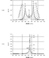
- FIG. 7A shows the frequency (voltage conversion ratio) of the ratio of the voltage V2 applied to the coupling electrode of the power receiving apparatus 201 to the voltage V1 applied to the coupling electrode of the power transmission apparatus 101 of the power transmission system according to the first embodiment. It is a figure which shows dependency.
- FIG. 7B is a diagram illustrating an example of the frequency dependence of the voltage conversion ratio of the comparative power transmission system ().
- FIG. 8 is a configuration diagram of a power transmission system according to the second embodiment.
- FIG. 9 is an equivalent circuit diagram of the power transmission system 402 of the second embodiment.
- FIG. 10 is an equivalent circuit diagram of the power transmission system 402 of the second embodiment.
- FIG. 11 shows the frequency dependence of the ratio (voltage conversion ratio) of the voltage V2 applied to the coupling electrode of the power receiving apparatus 202 to the voltage V1 applied to the coupling electrode of the power transmission apparatus 102 of the power transmission system of the second embodiment.
- FIG. 12 is an equivalent circuit diagram of the power transmission system 403 of the third embodiment.
- FIG. 2 is a configuration diagram of the power transmission system according to the first embodiment.
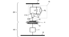
- the power transmission device 101 is provided with a power transmission device-side coupling electrode including an active electrode 13 and a passive electrode 12 on the power transmission device side.
- the power receiving apparatus 201 is provided with a power receiving apparatus side coupling electrode composed of an active electrode 16 and a passive electrode 17 on the power receiving apparatus side.
- the power receiving device 201 is provided with a power receiving circuit 15.
- the power receiving circuit 15 includes a piezoelectric transformer 32, an inductance element L2, and a load circuit RL.
- a reference potential terminal E12 of the piezoelectric transformer 32 is connected to the passive electrode 17 on the power receiving device side, and an inductance element L2 and a load circuit RL are connected between the passive electrode 17 and the output terminal E11.
- the voltage stepped down by the piezoelectric transformer 32 is supplied to the load circuit RL.
- the load circuit RL includes a rectifying / smoothing circuit and a load that operates with a DC voltage output from the rectifying / smoothing circuit.
- power is transmitted from the power transmission apparatus 101 to the power reception apparatus 201 via the high-voltage electric field region 4 with the power reception apparatus 201 mounted on the power transmission apparatus 101.
- the power transmission system of the present invention is based on short-range energy transmission using electric field coupling (quasi-static electric field). If the wavelength ⁇ is sufficiently long with respect to the size and operating range (distance d) of the electric field oscillation source, that is, if d / ⁇ ⁇ 1, the quasi-static electric field stays in the vicinity of the electric field generation source (binding). The amount of radiation far away is so small that it can be ignored. That is, energy is hardly emitted as electromagnetic waves.
- the electromagnetic wave is in a transverse mode (both the electric field and the magnetic field are perpendicular to the propagation direction), whereas in power transmission using a quasi-static electric field as in the present invention, the energy is in the same direction as the electric field. Is transmitted.
- the load includes, for example, a secondary battery for power supply of the power receiving apparatus 201, and the secondary battery in the power receiving apparatus 201 is charged by attaching the power receiving apparatus 201 to the power transmitting apparatus 101.
- FIG. 3 is a circuit diagram of the power transmission system 401 according to the first embodiment.
- the high frequency high voltage generation circuit 11 of the power transmission apparatus 101 generates a high frequency voltage of 100 kHz to several tens of MHz, for example.
- a voltage generated by the high frequency high voltage generation circuit 11 is applied between the passive electrode 12 and the active electrode 13.
- the capacitance element CG is a capacitance mainly composed of the passive electrode 12 and the active electrode 13.
- the capacitance element CL is a capacitance mainly composed of the passive electrode 17 and the active electrode 16.
- the piezoelectric transformer 32 steps down the voltage applied between the reference potential terminal E12 and the input terminal E20 and outputs it to the output terminal E11.
- the coupling of the coupling electrode by the passive electrode and the active electrode of the power transmission apparatus 101 and the coupling electrode by the passive electrode and the active electrode of the power reception apparatus 201 can be expressed as being coupled via the mutual capacitance Cm.
- the high frequency high voltage generation circuit 11 generates a high frequency high voltage of 100 to 3 kV, and the piezoelectric transformer 32 steps down the voltage 100 to 3 kV induced in the capacitance element CL to 5 to 12 V and outputs it to the load circuit RL.
- the output terminal E11 of the piezoelectric transformer 32 may be connected to the passive electrode 17 of the power receiving apparatus 201, and the inductance element L2 and the load circuit RL may be connected between the passive electrode 17 and the reference potential terminal E12. That is, the reference potential terminal E12 and the output terminal E11 may be interchanged.
- FIG. 4 is an equivalent circuit diagram of the power transmission system 401 of the first embodiment.
- the piezoelectric transformer 32 is represented by capacitance elements C1 and C2, an inductance element Lp, a capacitance element Cp, a resistor Rp, and an ideal transformer Tp.
- the capacitance element C2 is an equivalent output capacity of the piezoelectric transformer, and the capacitance element Cp and the inductance element Lp are electromechanical parameters.
- the resonance frequency of the piezoelectric transformer 32 is determined mainly by the resonance of the resonance circuit by the capacitance element Cp and the inductance element Lp. Since electrical energy conversion is via elastic vibration, it has a natural resonance frequency determined by the elastic wave propagation velocity and dimensions of the piezoelectric ceramic.
- the first resonance circuit RC1 is configured by the capacitance of the capacitance element CL of the coupling electrode portion of the piezoelectric transformer 32 and the power receiving device 201 and the capacitance element CG of the coupling electrode portion of the power transmission device 101.
- the resonance frequency of the first resonance circuit RC1 is determined by the circuit constant of the first resonance circuit RC1.
- the transmission power can be improved.
- the second resonance circuit RC2 is constituted by the capacitance element (capacitance component) C2 and the inductance element L2 which are equivalent output capacities of the piezoelectric transformer 32, and the capacitance of the capacitance element C2 and the inductance of the inductance element L2 are used.
- the resonance frequency of the second resonance circuit RC2 is determined.
- the frequency of the high-frequency high-voltage generated by the high-frequency high-voltage generation circuit 11 is determined between two resonance frequencies due to the composite resonance (coupled resonance) of the first resonance circuit RC1 and the second resonance circuit RC2.
- the inductance element L2 also functions as an impedance matching circuit between the load circuit RL and the piezoelectric transformer 32. Therefore, the standing wave in the first resonance circuit RC1 is reduced, unnecessary energy is not accumulated in the piezoelectric transformer 32, and energy flows smoothly to the load circuit RL. As a result, overheating of the piezoelectric transformer 32 is prevented.
- the power transmission device can be reduced in size and the leakage magnetic field can be suppressed as compared with the case where a winding transformer is used.
- FIG. 5A is a block configuration diagram of a high-frequency high-voltage generation circuit of the power transmission apparatus 101.
- the drive power supply circuit 51 is a power supply circuit that inputs a commercial power supply and generates a constant DC voltage (for example, DC 5 V).
- the control circuit 52 controls each unit by inputting / outputting signals to / from each unit described below.
- the drive control circuit 55 switches the switch element of the switching circuit 56 in accordance with the ON / OFF signal output from the control circuit 52. As will be described later, the switching circuit 56 alternately drives the input section of the booster circuit 37.
- the ACV detection circuit 58 capacitively divides the voltage applied to the active electrode 13 with the passive electrode 12 as a reference, and generates a DC voltage obtained by rectifying the divided AC voltage as a detection signal V (ACV).
- the ACV detection circuit 58 corresponds to a “voltage detection circuit” according to the present invention.
- the control circuit 52 reads the detection signal V (ACV) and feedback-controls the generated voltage of the high frequency high voltage generation circuit so that the detection signal V (ACV) becomes constant.
- the control circuit 52 that performs the feedback control corresponds to a “voltage stabilization circuit” according to the present invention.
- FIG. 5B is a diagram showing the relationship between the configuration of the switching circuit 56 and the drive control circuit 55.
- the switching circuit 56 performs a push-pull operation by turning on / off the high-side switch element and the low-side switch element, and alternately drives the booster circuit 37.
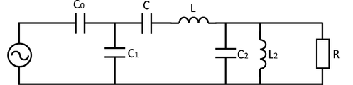
- FIG. 6 is another equivalent circuit diagram of the power transmission system 401 of the first embodiment.
- This equivalent circuit is an equivalent circuit in which the first resonance circuit and the second resonance circuit are combined.
- the capacitor Co corresponds to a capacitance component generated in the coupling electrode portion of the power transmitting device and the power receiving device
- the capacitor C corresponds to the capacitor Cp shown in FIG. 4
- the inductor L corresponds to the inductor Lp shown in FIG.
- FIG. 7A shows the frequency dependence of the ratio (voltage conversion ratio) of the voltage V2 applied to the load of the power receiving apparatus 201 to the voltage V1 applied to the coupling electrode of the power transmitting apparatus 101 of the power transmission system of the first embodiment. It is a figure which shows sex. Here, a case is shown in which the degree of coupling between the coupling electrode formed by the passive electrode and the active electrode of the power transmission apparatus 101 and the coupling electrode formed by the passive electrode and the active electrode of the power receiving apparatus 201 is constant and the load is varied.
- FIG. 7B is a diagram showing an example of the frequency dependence of the voltage conversion ratio of the comparative power transmission system.
- the power receiving device of this comparative power transmission system has a configuration in which the inductance element L2 shown in FIGS. 3 and 4 is not provided. Therefore, the power receiving apparatus of the comparative power transmission system does not have the second resonance circuit (RC2 in FIG. 4).
- characteristic curves (1) to (10) indicate characteristics at each resistance value when the resistance value of the load R is changed in the range of 10 ⁇ to 10 k ⁇ . .
- the voltage conversion ratio V2 / V1 increases as the load resistance increases, and may become excessive when there is no load. Recognize.
- the marker m17 in FIG. 7B is the voltage conversion ratio V2 / V1 at the rated load.
- the frequencies at which the voltage conversion ratio V2 / V1 becomes excessive are 280 kHz and 330 kHz, both of which are drive frequencies.
- the voltage conversion ratio V2 / V1 is kept substantially constant even when the drive frequency varies due to load variation or the like.
- the coupling frequency between the coupling electrode of the power transmission device and the coupling electrode of the power reception device is constant, and the frequency f0 at which the voltage conversion ratio V2 / V1 is maximum or minimum when the load is changed is the driving frequency.
- FIG. 6 shows that the minimum frequency when the resistance value of the load R approaches 10 k ⁇ from the low resistance side and the maximum frequency when the resistance value of the load R approaches 10 ⁇ from the high resistance side are matched. If the equivalent circuit constant is set and f0 is separated from f1 and f2, the fluctuation of the voltage conversion ratio V2 / V1 can be reduced.
- the slope of the voltage conversion ratio V2 / V1 with respect to the frequency is not steep and a stable circuit is obtained.
- a tracking control circuit that searches for a maximum frequency when approaching 10 ⁇ from the high resistance side can be configured relatively easily.
- the drive frequency fd is determined between the two resonance frequencies due to the composite resonance of the first resonance circuit RC1 and the second resonance circuit RC2, the change in the voltage conversion ratio V2 / V1 with respect to the frequency change is small. Therefore, the ratio V2 / V1 between the load side voltage V2 and the power transmission device side voltage V1 when the load fluctuates can be stabilized.
- the drive frequency fd is set to the frequency of the marker m17 (the frequency at which the voltage conversion ratio V2 / V1 at the rated load shows a peak) in FIG. 7A, even if the load fluctuates, the voltage conversion ratio V2 / V1 can be further stabilized.
- the drive frequency of the high frequency high voltage generation circuit 11 of the power transmission device is determined so that the voltage conversion ratio V2 / V1 is constant, high frequency high voltage generation is performed so that the voltage V1 on the power transmission device side is constant.
- the circuit 11 may be controlled. That is, the voltage V2 on the power receiving device side can be made constant by detecting the voltage V1 on the power transmitting device side and performing feedback control without directly monitoring the voltage V2 on the power receiving device side.
- control circuit 52 illustrated in FIG. 5A may control the duty of the switching circuit 56 via the drive control circuit 55.
- the voltage generated by the drive power supply circuit 51 may be controlled.
- the degree of coupling varies accordingly. In this way, when the degree of coupling varies, the voltage conversion ratio V2 / V1 changes. Therefore, the voltage generated by the high frequency high voltage generation circuit 11 may be changed according to the degree of coupling.
- the degree of coupling can be estimated by cooperation with the power receiving device side or by measuring the resonance frequency.
- the voltage V2 on the power receiving device side can be further stabilized by providing a voltage detector on the power receiving device side and feeding back the information to the power transmitting device side.
- the influence of the characteristic fluctuation on the frequency fluctuation can be effectively reduced.
- the piezoelectric transformer is used as the first resonance circuit, a configuration in which energy is not accumulated in the piezoelectric transformer can be realized, heat generation of the piezoelectric transformer can be suppressed, and the piezoelectric transformer can be efficiently taken out to the load.
- FIG. 8 is a configuration diagram of the power transmission system 402 of the second embodiment.
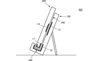
- the power transmission apparatus 102 includes a pedestal portion 10D and a backrest portion 10B orthogonal thereto.
- the power transmission device side passive electrode 12 is provided along the pedestal portion 10 ⁇ / b> D inside the casing of the power transmission device 102.
- a power transmission device side active electrode 13 is provided on the backrest portion 10B.
- the power receiving device side passive electrode 17 is provided in the lower part inside the housing of the power receiving device 202. Near the back surface, a power receiving device side active electrode 16 is provided.
- FIG. 9 is an equivalent circuit diagram of the power transmission system 402 of the second embodiment.
- the high frequency voltage generation circuit OSC of the power transmission apparatus 102 generates a high frequency voltage having a predetermined drive frequency.
- the booster circuit 37 using the booster transformer TG boosts the voltage generated by the high-frequency voltage generation circuit OSC and applies it between the passive electrode 12 and the active electrode 13 (see FIG. 8).
- the capacitance element CG is a capacitance mainly composed of the passive electrode 12 and the active electrode 13.
- a step-down transformer 45 by a step-down transformer TL is connected between the passive electrode 17 and the active electrode 16 of the power receiving device 201 (see FIG. 8).
- the capacitance element CL is a capacitance mainly composed of the passive electrode 17 and the active electrode 16.
- a load circuit RL is connected to the secondary side of the step-down transformer TL.
- the load circuit RL includes a rectifying / smoothing circuit using a diode and a capacitor, and a secondary battery.
- the coupling between the coupling electrode of the power transmitting apparatus 102 and the coupling electrode of the power receiving apparatus 202 can be expressed as coupled via a mutual capacitance Cm as shown in FIG.
- FIG. 10 is an equivalent circuit diagram of the power transmission system 402 of the second embodiment.
- the step-down transformer 45 is represented by a capacitance element C2, an inductance element Ls, a resistance Rs, and an ideal transformer T as shown in FIG.
- the inductance element Ls is an inductance component of the transformer
- the capacitance element C2 is a stray capacitance
- the resistance Rs is a resistance component of the winding.
- the first resonant circuit RC1 is configured by the capacitance of the capacitance element CL of the coupling electrode section of the step-down transformer 45 and the power receiving apparatus 202 and the capacitance of the capacitance element CG of the coupling electrode section of the power transmission apparatus 102.
- the resonance frequency is determined by the circuit constant of the first resonance circuit RC1.
- a second resonant circuit RC2 is configured by the capacitance element C2 and the inductance element L2 which are the stray capacitances, and the resonance of the second resonance circuit RC2 is formed by the capacitance of the capacitance element C2 and the inductance of the inductance element L2. The frequency is determined.
- the frequency of the high-frequency high-voltage generated by the high-frequency high-voltage generation circuit 31 is determined between two resonance frequencies due to the composite resonance of the first resonance circuit RC1 and the second resonance circuit RC2.
- FIG. 11 shows the frequency dependence of the ratio (voltage conversion ratio) of the voltage V2 applied to the load of the power receiving apparatus 202 to the voltage V1 applied to the coupling electrode of the power transmitting apparatus 102 of the power transmission system of the second embodiment.
- a case is shown in which the degree of coupling between the coupling electrode formed by the passive electrode and the active electrode of the power transmitting apparatus 102 and the coupling electrode formed by the passive electrode and the active electrode of the power receiving apparatus 202 is constant and the load is varied.
- characteristic curves (1) to (10) indicate characteristics at respective resistance values when the resistance value of the load circuit RL is changed in the range of 10 ⁇ to 10 k ⁇ . The larger the number in parentheses, the greater the load resistance value.
- the frequencies at which the voltage conversion ratio V2 / V1 becomes excessive are 0.2 MHz and 0.45 MHz, which are far from the driving frequency (about 0.3 MHz). Therefore, the voltage conversion ratio V2 / V1 is kept substantially constant even when the drive frequency varies due to load variation or the like.
- the driving frequency of the high frequency high voltage generation circuit 31 of the power transmission device is determined so that the voltage conversion ratio V2 / V1 is constant.
- the high frequency high voltage generation circuit 31 may be controlled so that the voltage V1 on the power transmission device side is constant. As a result, the voltage V2 on the power receiving device side can be made constant.
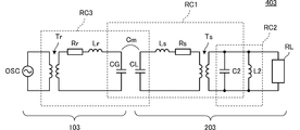
- FIG. 12 is an equivalent circuit diagram of the power transmission system 403 of the third embodiment.
- the power transmission system 403 includes a power transmission device 103 and a power reception device 203.
- the configuration of the power receiving apparatus 203 is the same as that of the power receiving apparatus 202 shown in the second embodiment.
- the power transmission device 103 includes a step-up transformer. This step-up transformer is represented by an ideal transformer Tr, a resistor Rr, and an inductance element Lr in FIG.
- the ideal transformer Tr, the resistor Rr, the inductance element Lr, and the capacitance elements CG and CL of the coupling electrode portion constitute a third resonance circuit RC3.
- the resonance frequency of the third resonance circuit RC3 is determined by the capacitances of the inductance element Lr and the capacitance elements CG and CL of the coupling electrode portion.
- the resonance frequency of the third resonance circuit RC3 is determined so as to resonate at the frequency of the high frequency voltage generated by the high frequency voltage generation circuit OSC.
- the third resonance circuit RC3 resonates with the high frequency high voltage applied to the power transmission device side coupling electrode, so that the boost ratio can be increased and the harmonics are resonated. Can be suppressed.
- the reactance component can be canceled, impedance matching is performed, and the power transmission efficiency from the power transmission apparatus to the power reception apparatus can be increased.
Abstract
Description
アクティブ電極およびパッシブ電極で構成される送電装置側結合電極、この送電装置側結合電極に高周波高電圧を印加する高周波高電圧発生回路を備えた送電装置と、
前記送電装置側結合電極に結合する、アクティブ電極およびパッシブ電極で構成される受電装置側結合電極および前記受電装置側結合電極に接続された受電回路を備えた受電装置と、を有し、
前記送電装置側結合電極および前記受電装置側結合電極が電界結合することにより前記送電装置から前記受電装置へ電力が伝送される。
前記高周波高電圧発生回路の発生する高周波高電圧の周波数は、第1の共振回路と第2の共振回路の複合共振による二つの共振周波数の間に設定されたことを特徴とする。
前記キャパシタンス成分は前記圧電トランスの等価出力容量であることが好ましい。
アクティブ電極およびパッシブ電極で構成される送電装置側結合電極およびこの送電装置側結合電極に高周波高電圧を印加する高周波高電圧発生回路を備えた送電装置に対して対をなす受電装置であって、
前記送電装置側結合電極に結合する、アクティブ電極およびパッシブ電極で構成される受電装置側結合電極および前記受電装置側結合電極に接続された受電回路、を有し、
前記受電回路は、前記受電装置側結合電極のアクティブ電極とパッシブ電極との間に直列接続された、インダクタンス成分およびキャパシタンス成分を含む第1の共振回路と、前記キャパシタンス成分とこのキャパシタンス成分に対して並列接続されたインダクタンス成分を含む第2の共振回路と、この第2の共振回路に並列接続された負荷回路とを備え、
前記高周波高電圧発生回路の発生する高周波高電圧の周波数は、第1の共振回路と第2の共振回路の複合共振による二つの共振周波数の間に設定されたことを特徴とする。
図2は第1の実施形態の電力伝送システムの構成図である。ここでは、特に送電装置101に受電装置201を装着した状態を表している。送電装置101には送電装置側のアクティブ電極13およびパッシブ電極12で構成される送電装置側結合電極が設けられている。受電装置201には受電装置側のアクティブ電極16およびパッシブ電極17で構成される受電装置側結合電極が設けられている。
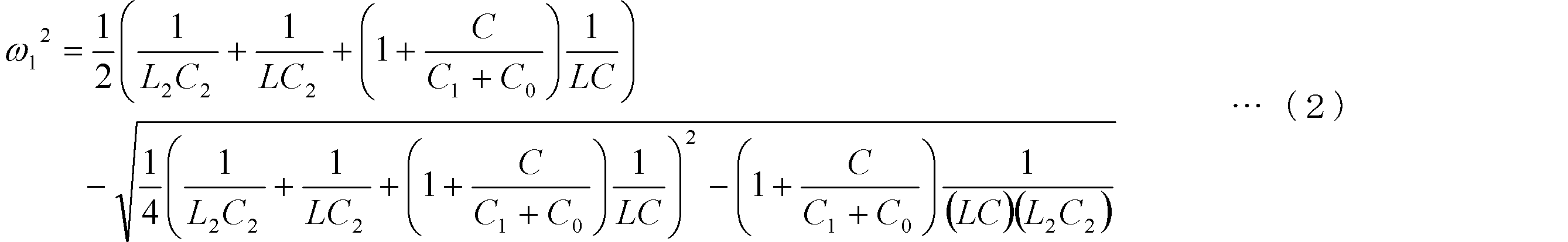

図8は第2の実施形態の電力伝送システム402の構成図である。ここでは、特に送電装置102に受電装置202を装着した状態での断面を表している。送電装置102は台座部10Dと、それに直交する背もたれ部10Bを備えている。送電装置102の筐体内部で台座部10Dに沿って送電装置側パッシブ電極12が設けられている。背もたれ部10Bには送電装置側アクティブ電極13が設けられている。受電装置202の筐体内部で下部に受電装置側パッシブ電極17が設けられている。背面付近には受電装置側アクティブ電極16が設けられている。
図12は第3の実施形態の電力伝送システム403の等価回路図である。この電力伝送システム403は送電装置103および受電装置203を備えている。受電装置203の構成は第2の実施形態で示した受電装置202と同じである。送電装置103は昇圧トランスを備えている。この昇圧トランスは図12における理想変圧器Tr、抵抗Rrおよびインダクタンス素子Lrで表される。この理想変圧器Tr、抵抗Rr、インダクタンス素子Lrおよび結合電極部のキャパシタンス素子CG,CLによって第3の共振回路RC3が構成されている。そしてインダクタンス素子Lrおよび結合電極部のキャパシタンス素子CG,CLのキャパシタンスによって第3の共振回路RC3の共振周波数が定まる。
CG,CL…キャパシタンス素子
Cm…相互容量
Cp…キャパシタンス素子
E11…出力端子
E12…基準電位端子
E20…入力端子
L2…インダクタンス素子
Lp…インダクタンス素子
Lr…インダクタンス素子
Ls…インダクタンス素子
OSC…高周波電圧発生回路
RC1…第1の共振回路
RC2…第2の共振回路
RC3…第3の共振回路
RL…負荷回路
Rp,Rr,Rs…抵抗
TG…昇圧トランス
TL…降圧トランス
T,Tp,Tr…理想変圧器
V…検出信号
V1…送電装置側電圧
V2…受電装置側電圧
11…高周波高電圧発生回路
12…送電装置側パッシブ電極
13…送電装置側アクティブ電極
15…受電回路
16…受電装置側アクティブ電極
17…受電装置側パッシブ電極
31…高周波高電圧発生回路
32…圧電トランス
37…昇圧回路
45…降圧トランス
51…駆動電源回路
52…制御回路
55…駆動制御回路
56…スイッチング回路
58…ACV検出回路
101~103…送電装置
201~203…受電装置
401~403…電力伝送システム
Claims (6)
- アクティブ電極およびパッシブ電極で構成される送電装置側結合電極、この送電装置側結合電極に高周波高電圧を印加する高周波高電圧発生回路を備えた送電装置と、
前記送電装置側結合電極に結合する、アクティブ電極およびパッシブ電極で構成される受電装置側結合電極および前記受電装置側結合電極に接続された受電回路を備えた受電装置と、を有し、
前記送電装置側結合電極および前記受電装置側結合電極が電界結合することにより前記送電装置から前記受電装置へ電力が伝送される電力伝送システムにおいて、
前記受電回路は、前記受電装置側結合電極のアクティブ電極とパッシブ電極との間に直列接続された、インダクタンス成分およびキャパシタンス成分を含む第1の共振回路と、前記キャパシタンス成分とこのキャパシタンス成分に対して並列接続されたインダクタンス成分を含む第2の共振回路と、この第2の共振回路に並列接続された負荷回路とを備え、
前記高周波高電圧発生回路の発生する高周波高電圧の周波数は、第1の共振回路と第2の共振回路の複合共振による二つの共振周波数の間に設定されたことを特徴とする電力伝送システム。 - 前記送電装置は、前記高周波高電圧発生回路の発生電圧を検出する電圧検出回路と、この電圧検出回路の検出電圧が一定となるように前記高周波高電圧発生回路の発生電圧を制御する電圧安定化回路とを備えた、請求項1に記載の電力伝送システム。
- 前記受電回路は、前記受電装置側結合電極のアクティブ電極に接続された入力端子と、前記受電装置側結合電極のパッシブ電極に接続された出力端子と、基準電位端子とを有して、前記入力端子に印加される電圧を降圧して前記出力端子へ出力する圧電トランスを備え、
前記キャパシタンス成分は前記圧電トランスの等価出力容量である、請求項1または2に記載の電力伝送システム。 - 前記第1の共振回路は、前記送電装置側結合電極および前記受電装置側結合電極に生じるキャパシタンス成分を含む、請求項1~3にいずれかに記載の電力伝送システム。
- 前記高周波高電圧発生回路は、前記送電装置側結合電極に印加される前記高周波高電圧に共振する第3の共振回路を備える、請求項1~4にいずれかに記載の電力伝送システム。
- アクティブ電極およびパッシブ電極で構成される送電装置側結合電極およびこの送電装置側結合電極に高周波高電圧を印加する高周波高電圧発生回路を備えた送電装置に対して対をなす受電装置であって、
前記送電装置側結合電極に結合する、アクティブ電極およびパッシブ電極で構成される受電装置側結合電極および前記受電装置側結合電極に接続された受電回路、を有し、
前記受電回路は、前記受電装置側結合電極のアクティブ電極とパッシブ電極との間に直列接続された、インダクタンス成分およびキャパシタンス成分を含む第1の共振回路と、前記キャパシタンス成分とこのキャパシタンス成分に対して並列接続されたインダクタンス成分を含む第2の共振回路と、この第2の共振回路に並列接続された負荷回路とを備え、
前記高周波高電圧発生回路の発生する高周波高電圧の周波数は、第1の共振回路と第2の共振回路の複合共振による二つの共振周波数の間に設定されたことを特徴とする受電装置。
Priority Applications (4)
| Application Number | Priority Date | Filing Date | Title |
|---|---|---|---|
| GB1313264.2A GB2502903A (en) | 2011-06-13 | 2012-05-21 | Power transmission system and power reception device |
| CN201280015569.4A CN103477534B (zh) | 2011-06-13 | 2012-05-21 | 电力传输系统以及受电装置 |
| JP2013520486A JP5590237B2 (ja) | 2011-06-13 | 2012-05-21 | 電力伝送システムおよび受電装置 |
| US14/017,698 US9531216B2 (en) | 2011-06-13 | 2013-09-04 | Power transmission system and power receiving apparatus |
Applications Claiming Priority (2)
| Application Number | Priority Date | Filing Date | Title |
|---|---|---|---|
| JP2011131094 | 2011-06-13 | ||
| JP2011-131094 | 2011-06-13 |
Related Child Applications (1)
| Application Number | Title | Priority Date | Filing Date |
|---|---|---|---|
| US14/017,698 Continuation US9531216B2 (en) | 2011-06-13 | 2013-09-04 | Power transmission system and power receiving apparatus |
Publications (1)
| Publication Number | Publication Date |
|---|---|
| WO2012172929A1 true WO2012172929A1 (ja) | 2012-12-20 |
Family
ID=47356923
Family Applications (1)
| Application Number | Title | Priority Date | Filing Date |
|---|---|---|---|
| PCT/JP2012/062902 WO2012172929A1 (ja) | 2011-06-13 | 2012-05-21 | 電力伝送システムおよび受電装置 |
Country Status (5)
| Country | Link |
|---|---|
| US (1) | US9531216B2 (ja) |
| JP (2) | JP5590237B2 (ja) |
| CN (1) | CN103477534B (ja) |
| GB (1) | GB2502903A (ja) |
| WO (1) | WO2012172929A1 (ja) |
Cited By (4)
| Publication number | Priority date | Publication date | Assignee | Title |
|---|---|---|---|---|
| JP2015053781A (ja) * | 2013-09-06 | 2015-03-19 | 株式会社村田製作所 | 電力変換器 |
| WO2015050095A1 (ja) * | 2013-10-03 | 2015-04-09 | 株式会社村田製作所 | 送電装置、受電装置及びワイヤレス電力伝送システム |
| WO2015053246A1 (ja) * | 2013-10-09 | 2015-04-16 | 株式会社村田製作所 | ワイヤレス電力伝送システム |
| JP2017005790A (ja) * | 2015-06-05 | 2017-01-05 | Tdk株式会社 | ワイヤレス電力伝送システム |
Families Citing this family (4)
| Publication number | Priority date | Publication date | Assignee | Title |
|---|---|---|---|---|
| US9775200B2 (en) * | 2014-02-12 | 2017-09-26 | Philips Lighting Holding B.V. | Illumination system comprising an array of LEDs |
| US9673658B2 (en) * | 2014-03-06 | 2017-06-06 | Samsung Electro-Mechanics Co., Ltd. | Non-contact capacitive coupling type power charging apparatus and non-contact capacitive coupling type battery apparatus |
| CN107409007B (zh) | 2015-03-03 | 2019-12-24 | 华为技术有限公司 | 用于调度终端设备的方法和网络设备 |
| US20210281123A1 (en) * | 2020-03-05 | 2021-09-09 | Powermat Technologies Ltd. | Dynamic resonance for wireless power systems |
Citations (4)
| Publication number | Priority date | Publication date | Assignee | Title |
|---|---|---|---|---|
| JPH0538232U (ja) * | 1991-10-25 | 1993-05-25 | 株式会社東海理化電機製作所 | 車両用キー装置 |
| JPH09312942A (ja) * | 1996-05-21 | 1997-12-02 | Hitachi Ltd | 非接触式集電方法およびその装置 |
| JP2009296857A (ja) * | 2008-06-09 | 2009-12-17 | Sony Corp | 伝送システム、給電装置、受電装置、及び伝送方法 |
| JP2010537613A (ja) * | 2007-08-17 | 2010-12-02 | Tmms株式会社 | 電気双極子間の近接場における遠隔縦結合によって電気エネルギを伝達し、分配し、かつ管理するための方法および装置 |
Family Cites Families (9)
| Publication number | Priority date | Publication date | Assignee | Title |
|---|---|---|---|---|
| JPH0538232A (ja) | 1991-08-07 | 1993-02-19 | Nippon Steel Chem Co Ltd | 育苗マツト充填方法及び装置 |
| JPH09312842A (ja) * | 1996-05-23 | 1997-12-02 | Ekushingu:Kk | Mpegデータ再生装置及びその再生装置を備えたmpegデータ供給・再生システム |
| JPH1092673A (ja) * | 1996-07-26 | 1998-04-10 | Tdk Corp | 非接触電力伝送装置 |
| JP2002111090A (ja) | 2000-09-27 | 2002-04-12 | Nagano Japan Radio Co | 圧電トランスおよび圧電トランスの駆動方法 |
| BRPI0621437A2 (pt) | 2006-03-21 | 2012-07-10 | Tmms Co Ltd | dispositivos de transporte da eletricidade através do vácuo e de materiais dielétricos |
| JP5375032B2 (ja) * | 2008-11-04 | 2013-12-25 | 株式会社豊田自動織機 | 非接触電力伝送装置及び非接触電力伝送装置の設計方法 |
| JP5093386B2 (ja) * | 2010-08-25 | 2012-12-12 | 株式会社村田製作所 | 送電装置および電力伝送システム |
| WO2012157012A1 (en) * | 2011-05-13 | 2012-11-22 | Murata Manufacturing Co., Ltd. | Power transmitting device, power receiving device, and power transmission system |
| JP5884830B2 (ja) * | 2011-10-27 | 2016-03-15 | トヨタ自動車株式会社 | 非接触受電装置、非接触送電装置および非接触送受電システム |
-
2012
- 2012-05-21 JP JP2013520486A patent/JP5590237B2/ja active Active
- 2012-05-21 GB GB1313264.2A patent/GB2502903A/en not_active Withdrawn
- 2012-05-21 CN CN201280015569.4A patent/CN103477534B/zh active Active
- 2012-05-21 WO PCT/JP2012/062902 patent/WO2012172929A1/ja active Application Filing
-
2013
- 2013-09-04 US US14/017,698 patent/US9531216B2/en active Active
-
2014
- 2014-07-22 JP JP2014148489A patent/JP5871034B2/ja active Active
Patent Citations (4)
| Publication number | Priority date | Publication date | Assignee | Title |
|---|---|---|---|---|
| JPH0538232U (ja) * | 1991-10-25 | 1993-05-25 | 株式会社東海理化電機製作所 | 車両用キー装置 |
| JPH09312942A (ja) * | 1996-05-21 | 1997-12-02 | Hitachi Ltd | 非接触式集電方法およびその装置 |
| JP2010537613A (ja) * | 2007-08-17 | 2010-12-02 | Tmms株式会社 | 電気双極子間の近接場における遠隔縦結合によって電気エネルギを伝達し、分配し、かつ管理するための方法および装置 |
| JP2009296857A (ja) * | 2008-06-09 | 2009-12-17 | Sony Corp | 伝送システム、給電装置、受電装置、及び伝送方法 |
Non-Patent Citations (1)
| Title |
|---|
| TOMOFUMI YAMASHITA: "Novel Power-Saving Type Inverter with Piezo-Electric Transformer for Back Light of Liquid Crystal Panel", RICOH TECHNICAL REPORT, vol. 31, no. 31, 2 August 2012 (2012-08-02), pages 59 - 66, Retrieved from the Internet <URL:http://www.ricoh.co.jp/about/company/technology/techreport/31/pdf/A3108.pdf> [retrieved on 20120802] * |
Cited By (6)
| Publication number | Priority date | Publication date | Assignee | Title |
|---|---|---|---|---|
| JP2015053781A (ja) * | 2013-09-06 | 2015-03-19 | 株式会社村田製作所 | 電力変換器 |
| WO2015050095A1 (ja) * | 2013-10-03 | 2015-04-09 | 株式会社村田製作所 | 送電装置、受電装置及びワイヤレス電力伝送システム |
| JP5935950B2 (ja) * | 2013-10-03 | 2016-06-15 | 株式会社村田製作所 | 送電装置、受電装置及びワイヤレス電力伝送システム |
| WO2015053246A1 (ja) * | 2013-10-09 | 2015-04-16 | 株式会社村田製作所 | ワイヤレス電力伝送システム |
| JP5862844B2 (ja) * | 2013-10-09 | 2016-02-16 | 株式会社村田製作所 | ワイヤレス電力伝送システム |
| JP2017005790A (ja) * | 2015-06-05 | 2017-01-05 | Tdk株式会社 | ワイヤレス電力伝送システム |
Also Published As
| Publication number | Publication date |
|---|---|
| JP2014212697A (ja) | 2014-11-13 |
| CN103477534A (zh) | 2013-12-25 |
| JP5871034B2 (ja) | 2016-03-01 |
| JP5590237B2 (ja) | 2014-09-17 |
| GB2502903A (en) | 2013-12-11 |
| CN103477534B (zh) | 2015-08-12 |
| GB201313264D0 (en) | 2013-09-11 |
| US9531216B2 (en) | 2016-12-27 |
| US20140009002A1 (en) | 2014-01-09 |
| JPWO2012172929A1 (ja) | 2015-02-23 |
Similar Documents
| Publication | Publication Date | Title |
|---|---|---|
| JP5871034B2 (ja) | 電力伝送システムおよび受電装置 | |
| CN107257167B (zh) | 送电装置以及无线电力传输系统 | |
| US7999414B2 (en) | Apparatus and method for wireless energy and/or data transmission between a source device and at least one target device | |
| JP6009043B2 (ja) | 非接触電力伝送装置 | |
| JP5426570B2 (ja) | 誘導電力転送回路 | |
| KR101436063B1 (ko) | 무선 전력 송수신 장치 | |
| WO2010101078A1 (ja) | 非接触電力供給装置及び方法 | |
| JP5299578B2 (ja) | 電力送電装置及び電力伝送システム | |
| JP5516824B2 (ja) | 電力伝送システム | |
| CA2639155A1 (en) | Apparatus and method for wireless energy and/or data transmission between a source device and at least one target device | |
| JP5862844B2 (ja) | ワイヤレス電力伝送システム | |
| EP2603964A1 (en) | Wireless energy transmission | |
| JP5949773B2 (ja) | 受電装置およびそれを備える車両、ならびに電力伝送システム | |
| JP2012110199A (ja) | 電力伝送システム | |
| KR102630557B1 (ko) | 무선전력 송신장치 | |
| CN101179207A (zh) | 一种无线电能传输、充电方法及其装置 | |
| JP2012110211A (ja) | 電力伝送システム | |
| JP2012034524A (ja) | 無線電力伝送装置 | |
| JP6112222B2 (ja) | 周波数特性測定方法 | |
| JP2013081331A (ja) | 非接触電力伝送装置 | |
| KR101413490B1 (ko) | 무선전력 전송장치 및 이를 이용한 무선충전공간을 구축하는 방법 | |
| JP2013165617A (ja) | 非接触給電装置及びそれを用いた非接触給電システム |
Legal Events
| Date | Code | Title | Description |
|---|---|---|---|
| 121 | Ep: the epo has been informed by wipo that ep was designated in this application |
Ref document number: 12800851 Country of ref document: EP Kind code of ref document: A1 |
|
| ENP | Entry into the national phase |
Ref document number: 2013520486 Country of ref document: JP Kind code of ref document: A |
|
| ENP | Entry into the national phase |
Ref document number: 1313264 Country of ref document: GB Kind code of ref document: A Free format text: PCT FILING DATE = 20120521 |
|
| WWE | Wipo information: entry into national phase |
Ref document number: 1313264.2 Country of ref document: GB |
|
| NENP | Non-entry into the national phase |
Ref country code: DE |
|
| 122 | Ep: pct application non-entry in european phase |
Ref document number: 12800851 Country of ref document: EP Kind code of ref document: A1 |
|
| ENPC | Correction to former announcement of entry into national phase, pct application did not enter into the national phase |
Ref country code: GB |