WO2012169070A1 - 有機発光素子及びその製造方法 - Google Patents
有機発光素子及びその製造方法 Download PDFInfo
- Publication number
- WO2012169070A1 WO2012169070A1 PCT/JP2011/063381 JP2011063381W WO2012169070A1 WO 2012169070 A1 WO2012169070 A1 WO 2012169070A1 JP 2011063381 W JP2011063381 W JP 2011063381W WO 2012169070 A1 WO2012169070 A1 WO 2012169070A1
- Authority
- WO
- WIPO (PCT)
- Prior art keywords
- light emitting
- bus line
- layer
- organic material
- organic
- Prior art date
- Legal status (The legal status is an assumption and is not a legal conclusion. Google has not performed a legal analysis and makes no representation as to the accuracy of the status listed.)
- Ceased
Links
Images





Classifications
-
- H—ELECTRICITY
- H10—SEMICONDUCTOR DEVICES; ELECTRIC SOLID-STATE DEVICES NOT OTHERWISE PROVIDED FOR
- H10K—ORGANIC ELECTRIC SOLID-STATE DEVICES
- H10K50/00—Organic light-emitting devices
- H10K50/10—OLEDs or polymer light-emitting diodes [PLED]
- H10K50/14—Carrier transporting layers
- H10K50/15—Hole transporting layers
-
- H—ELECTRICITY
- H10—SEMICONDUCTOR DEVICES; ELECTRIC SOLID-STATE DEVICES NOT OTHERWISE PROVIDED FOR
- H10K—ORGANIC ELECTRIC SOLID-STATE DEVICES
- H10K59/00—Integrated devices, or assemblies of multiple devices, comprising at least one organic light-emitting element covered by group H10K50/00
- H10K59/80—Constructional details
- H10K59/805—Electrodes
- H10K59/8051—Anodes
- H10K59/80516—Anodes combined with auxiliary electrodes, e.g. ITO layer combined with metal lines
-
- H—ELECTRICITY
- H10—SEMICONDUCTOR DEVICES; ELECTRIC SOLID-STATE DEVICES NOT OTHERWISE PROVIDED FOR
- H10K—ORGANIC ELECTRIC SOLID-STATE DEVICES
- H10K71/00—Manufacture or treatment specially adapted for the organic devices covered by this subclass
- H10K71/10—Deposition of organic active material
- H10K71/12—Deposition of organic active material using liquid deposition, e.g. spin coating
- H10K71/13—Deposition of organic active material using liquid deposition, e.g. spin coating using printing techniques, e.g. ink-jet printing or screen printing
- H10K71/135—Deposition of organic active material using liquid deposition, e.g. spin coating using printing techniques, e.g. ink-jet printing or screen printing using ink-jet printing
Definitions
- the present invention relates to an organic light emitting device having an organic multilayer structure including an organic light emitting layer and a method for manufacturing the same.
- the bank is generally formed as an insulating film having almost no translucency. Therefore, since the light generated by driving the organic light emitting element is absorbed by the bank, there is a problem that the area of the region that guides the generated light to the outside is limited and power is consumed wastefully. That is, since the opening formed by the bank becomes a region that emits light to the outside as it is, the aperture ratio is lowered, and as a result, there is a problem that power consumption increases to obtain a desired light amount.
- the problem to be solved by the present invention is to provide the organic light emitting device capable of reducing the power consumption by increasing the aperture ratio by taking the above drawback as an example, and a method for manufacturing the same. Is the purpose.
- the organic light-emitting device covers a transparent substrate, a bus line pair made of a metal material juxtaposed on the substrate, and a region between the bus line pair and the bus line of the bus line pair.
- a method for manufacturing an organic light emitting device comprising: a bus line forming step of juxtaposing a bus line pair made of a metal material on a transparent substrate; and a region between the bus line pair and the bus line pair. And a step of forming an organic material layer by applying a solution containing an organic material onto the transparent conductive film.
- the bus line pair is juxtaposed on the substrate, and the bus line pair and the region between the bus lines are A transparent conductive film is formed so as to cover, an organic material layer is formed by applying an organic material on the transparent conductive film, and the generated light is diffused through the bus line of the metal material.
- the aperture ratio can be improved as compared with the conventional element.
- the power consumption can be reduced than that of a conventional element in order to obtain a desired light amount.
- FIG. 1 shows a method for manufacturing an organic light emitting device (organic EL device) to which the present invention is applied.
- the manufacturing method of FIG. 1 shows a method for manufacturing one organic light emitting element in a light emitting panel having a plurality of organic light emitting elements.
- this manufacturing method includes (a) a bus line formation step, (b) an anode formation step, (c) a hole injection / transport layer formation step, and (d) a coated light emitting layer formation. And (e) a vapor deposition layer forming step.
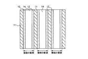
- Bus line forming step For example, a film is deposited and formed on a transparent (including translucent) substrate 11 made of a glass plate having a thickness of 0.7 mm using AlNd (aluminum-neodymium alloy) as a material by sputtering. Thereafter, a resist is applied onto the AlNd film by photolithography, and exposure and development are sequentially performed to transfer the mask pattern onto the resist. Further, the AlNd film other than the portion to be left as a bus line is removed by etching. The When the resist is removed on the substrate 11, the remaining AlNd film is obtained as a pair of bus lines 12 as shown in FIG.
- the bus line 12 has conductivity and is a power supply line to the anode 14 described later.
- the bus lines 12 have the same shape and are arranged in parallel with each other, and a pair of bus lines 12 form a recess therebetween.
- each bus line 12 has a thickness of 150 nm, a width of 50 ⁇ m, a distance between a pair of bus lines is 300 ⁇ m, and a gap between one of the pair of bus lines 12 and a bus line adjacent thereto. 50 ⁇ m.
- FIG. 1A shows a cross-section in the juxtaposition direction orthogonal to the line extending direction of the bus line 12, and this also applies to FIGS. 1B to 1D.
- Anode formation step A transparent film is deposited and formed on the substrate 11 including the bus line 12 by sputtering using IZO (indium zinc oxide) as a material, and then a resist is applied on the IZO film by photolithography.
- IZO indium zinc oxide
- photolithography In order to transfer the mask pattern to the resist, exposure and development are sequentially performed, and the IZO film other than the portion to be left as the anode is removed by etching.
- the resist is removed on the substrate 11, the remaining IZO film is obtained as a transparent anode 14 (transparent conductive film) as shown in FIG. 1 (b).
- the anode 14 is formed so as to cover both the pair of bus lines 12 and a region (concave portion) sandwiched between the bus lines 12, and is directly positioned on the substrate 11 in the region between the pair of bus lines 12.
- the thickness of the anode 14 is, for example, 180 nm.
- FIG. 2 is a plan view of the substrate 11 in which the anode 14 is formed on the substrate 11 together with a plurality of pairs of bus lines 12.
- (c) Hole injection / transport layer forming step First, the anode 14 is irradiated with UV / O 3 (ultraviolet / ozone) using an excimer light irradiation device (not shown), and the IZO surface is cleaned as a pretreatment. Is done. After the pretreatment, an organic material solution for hole injection / transport layer formation is applied using an ink jet method.
- UV / O 3 ultraviolet / O 3
- an ink 15 having a fixed concentration of 1 wt% using PEDOT (3,4-ethylenedioxythiophene polymer) as a host and PSS (styrene sulfonic acid polymer) as a dopant is shown in FIG.
- the ink 15 is on the anode 14 between one end thereof (the left end portion in the cross section of the anode 14 in FIG. 1C) and the other end portion (the right end portion in the cross section of the anode 14 in FIG. 1C). With the surface tension, the center is raised and raised so that it does not leak out from the end.
- the cross-sectional shape of the bus line 12 is narrowed toward the substrate 11, and the end face of the anode 14 is formed to be a substantially continuous plane with the bus line 12, It is possible to prevent the ink 15 from leaking outside the end portion at the end portion of the anode 14.
- both side surfaces of the bus lines 12 in the juxtaposition direction are inclined so as to become narrower toward the substrate 11, but at least the non-opposing side surfaces of the bus lines 12 in the juxtaposition direction face the substrate 11. It just needs to be inclined.
- the AlNd of the bus line 12 is etched together with the IZO film. Therefore, the AlNd portion on the side surface of the bus line 12 is largely removed. As a result, as shown in FIG. 4, the side surface of the bus line 12 following the end surface of the anode 14 is reversely tapered when viewed from the substrate 11. It may be used to form.
- the ink 15 is vacuum-dried at a gas pressure of 0.1 to 50 Pa for 2 minutes using a vacuum drying apparatus (not shown), and baked by heat treatment at 230 ° C. for 1 hour. .
- a hole injection / transport layer 16 in which the solvent of the ink 15 is evaporated and cured is obtained (organic material layer).
- the thickness of the hole injection / transport layer 16 is, for example, 30 nm.
- Coating light emitting layer forming step Also in this step, a solution of an organic material for forming a light emitting layer is applied using an inkjet method.
- an ink (6 wt% -Hex-Ir (phq) 3 : Balq) 17 having a fixed concentration of 2 wt% using Balq as a host and 6 wt% -Hex-Ir (phq) 3 as a dopant in an ink jet apparatus is obtained.
- it is applied by dropping into the recesses between the bus lines 12.
- the ink 17 is in a state where the center of the hole injection / transport layer 16 is raised between one end and the other end so as not to leak out from the end. That is, the taper angle at the end is increased by the wet pinning effect, so that the ink 17 does not leak to the outside of the end at the end of the hole injection / transport layer 16.
- the ink 17 is vacuum-dried for 2 minutes at a gas pressure of 0.1 to 50 Pa using a vacuum drying apparatus (not shown), and baked by heat treatment at 130 ° C. for 10 minutes.
- a vacuum drying apparatus not shown
- the thickness of the RG coating mixed layer 18 is 40 nm, for example.
- the host PAND and the dopant DPAVBi are vacuum-deposited together on the RG coating mixed layer 18 by a vacuum deposition method so that the dopant becomes 6 wt%. Formed with thickness.
- FIG. 1 (e) shows a blue light emitting layer 19, an electron transport layer 20, an electron injection layer 21, and a cathode 22 formed in this vapor deposition layer forming step.
- bus line forming step (b) anode forming step, (c) hole injection / transport layer forming step, (d) coating light emitting layer forming step, and (e) vapor deposition layer forming step are sequentially executed.
- an organic light emitting device is manufactured.
- a metal material such as AlNd is used as the bus line 12 and the anode 14 of the transparent conductive film is laminated on the bus line 12, so that the light generated in the organic light emitting layer is the bus line. 12 is diffused at 12 and emitted through the substrate 11, so that the aperture ratio of the organic light emitting device can be increased.
- an insulating bank material is used, and the bank material generally has a material that absorbs in the visible region, such as a polyimide material, and thus has a metal color of the cathode. Deteriorates appearance with respect to hue. Moreover, since there is an absorbing material in the visible region, the emitted light may be lost in the bank.
- the appearance is the same as the Al metal color of the cathode 22, and the appearance is not impaired.
- the electrical resistivity of the material of the bus line 12 is smaller than that of the material of the anode 14 and the anode 14 is in direct contact with the bus line 12, so that the organic light emitting device can be efficiently supplied with power.
- light emitted for increasing the aperture ratio can be emitted more efficiently, so that power consumption can be reduced compared to conventional devices in order to obtain a desired amount of light.
- the hole injection / transport layer 16 is formed by dropping the ink 15 in the recesses between the bus lines 12 and the RG coating mixed layer 18 is formed by dropping the ink 17.
- the two layers are not formed by using the wet pinning effect, and only one layer or three or more layers may be formed by using the wet pinning effect.
- the first light-emitting element A of the light-emitting panel includes (a) a bus line forming step, (b) an anode forming step, and (c) a hole injection / transport layer forming step as in the above-described embodiment. , (D) a coating light emitting layer forming step, and (e) a vapor deposition layer forming step.
- the second light emitting element B adjacent to the first light emitting element A is formed by (a) a bus line forming step, (b) an anode forming step, (c) a hole injection / transport layer forming step, and (e) a vapor deposition layer forming step. It is manufactured.
- the vapor deposition layer forming process is a process common to the first light emitting element A and the second light emitting element B, and each vapor deposition layer is continuously formed over the first light emitting element A and the second light emitting element B. .
- the layer formed by utilizing the wetting pinning effect is only the hole injection / transport layer 16, and (e) only blue light is emitted by the blue light emitting layer 19 formed by vapor deposition in the vapor deposition layer forming process. Obtained as a color. Further, in the light emitting panel shown in FIG.
- the uneven state of the surface of the hole injection / transport layer 16 coated and formed in the recesses is absorbed by the formation of the blue light emitting layer 19, and the surface of the blue light emitting layer 19 is flattened.
- An electron transport layer 20, an electron injection layer 21, and a cathode 22 are formed flat without unevenness for each element.
- the blue light emitting layer 19, the electron transport layer 20, the electron injection layer 21, and the cathode 22 are uneven without absorbing the above uneven state in each of the first light emitting element A and the second light emitting element B. It may be formed in a shape.
- the bus line 12 is formed directly on the substrate 11. However, as shown in FIG. 7, after the raised layer 24 made of an insulating material such as SiO 2 is formed on the substrate 11.
- the bus line 25 may be formed on the raised layer 24. In this way, the bus line 25 can be formed as a thin film from the bus line 12.
- the bus line 12 is shown as a power supply line in contact with the anode 14, it may be formed as a power supply line in contact with the cathode.
- the substrate 11 may be a transparent (including translucent) plastic substrate.
- metals such as Al, Ag, Mo, Ti, Pt, Au, or alloys thereof can be used, and those having a particularly high light reflectance are suitable.
- other metal oxides such as ITO can be used.
- the material of the hole injection / transport layer 16 other metal oxides such as Ag, Mo, Cr, and Ir that can drop ink can be used.
- the organic material of the light emitting layer such as the RG coating mixed layer 18 and the blue light emitting layer 19 may be an organic material having a function of emitting light by generating an excited state by injecting and recombining holes and electrons.
- the material of the electron injection layer 21 is preferably formed of barium, phthalocyanine, lithium fluoride, or a combination thereof.
- a metal oxide such as ITO or IZO may be used as a metal oxide such as ITO or IZO may be used.
- bus lines are formed as a pair, but the pair of bus lines need not have the same cross-sectional shape as each other, and do not have to have the same length in the line extending direction.
- the organic light emitting device and the manufacturing method thereof of the present invention can be applied to a light emitting device of an organic EL display or an organic EL lighting device.
- Substrate 12 25 Bus line 14 Anode 16 Hole injection / transport layer 18 RG coating mixed layer 19 Blue light emitting layer 20 Electron transport layer 21 Electron injection layer 22 Cathode
Landscapes
- Physics & Mathematics (AREA)
- Optics & Photonics (AREA)
- Engineering & Computer Science (AREA)
- Manufacturing & Machinery (AREA)
- Electroluminescent Light Sources (AREA)
Abstract
透明基板上に並置された金属材料からなるバスライン対と、バスライン対と前記バスライン対のバスライン間の領域とを覆うように形成された透明導電性膜と、透明導電性膜上への有機材料を含む溶液の塗布によって形成された有機材料層と、を含む有機発光素子。
Description
本発明は、有機発光層を含む有機多層構造の有機発光素子及びその製造方法に関する。
有機多層構造を含む有機EL素子等の有機発光素子を製造するために基板上にバンクを形成することはよく知られている(特許文献1及び2参照)。例えば、有機EL表示装置でマトリックス状に配置された各有機EL素子においては、基板上に陽極が形成されており、その陽極上には1対のバンクによって凹形状の開口部が形成される。バンクとしてはポリイミド等の絶縁性の材料が用いられており、バンクの表面は撥液性を有している。バンク間の開口部には例えば、インクジェット法を用いた有機材料の塗布によって有機材料層が形成される。そして、開口部の有機材料層に接触するように陰極が形成される。
しかしながら、上記したようなバンク構造の有機発光素子においては、バンクが一般に透光性がほとんどない絶縁膜として形成されている。よって、有機発光素子の駆動によって生成された光がバンクで吸収されるので、生成された光を外部に導く領域の面積が制限され、無駄に電力が消費されるという問題があった。すなわち、バンクによって形成された上記の開口部がそのまま光を外部に放出する領域となるので、開口率が低下し、結果として所望の光量を得るために消費電力が増加するという問題があった。
そこで、本発明が解決しようとする課題は、上記の欠点が一例として挙げられ、開口率を増加させて消費電力を低減させることができる有機発光素子及びその製造方法を提供することが本発明の目的である。
請求項1に係る発明の有機発光素子は、透明基板と、前記基板上に並置された金属材料からなるバスライン対と、前記バスライン対と前記バスライン対のバスライン間の領域とを覆うように形成された透明導電性膜と、前記透明導電性膜上への有機材料を含む溶液の塗布によって形成された有機材料層と、を含むことを特徴としている。
請求項7に係る発明の有機発光素子の製造方法は、透明基板上に金属材料からなるバスライン対を並置させるバスライン形成工程と、前記バスライン対と前記バスライン対のバスライン間の領域とを覆うように透明導電性膜を形成する工程と、前記透明導電性膜上への有機材料を含む溶液の塗布によって有機材料層を形成する工程と、を含むことを特徴としている。
請求項1に係る発明の有機発光素子及び請求項7に係る発明の有機発光素子の製造方法によれば、基板上にバスライン対が並置され、バスライン対とそのバスライン間の領域とを覆うように透明導電性膜が形成され、透明導電性膜上への有機材料の塗布によって有機材料層が形成され、生成された光が金属材料のバスラインで拡散されるので、有機発光素子の開口率を従来の素子より向上させることができる。また、生成された光を効率より放出させることができるので、所望の光量を得るために従来の素子より消費電力を低減させることができる。
以下、本発明の実施例を、図面を参照しつつ詳細に説明する。
図1は本発明が適用された有機発光素子(有機EL素子)の製造方法を示している。図1の製造方法では複数の有機発光素子を有する発光パネルにおける1つの有機発光素子の製造方法が示されている。この製造方法は図1(a)~(d)に示すように(a)バスライン形成工程、(b)陽極形成工程、(c)ホール注入・輸送層形成工程、(d)塗布発光層形成工程、及び(e)蒸着層形成工程を有する。
(a)バスライン形成工程
例えば、厚さ0.7mmのガラス板からなる透明(半透明を含む)な基板11上にスパッタ法によりAlNd(アルミニウム-ネオジウム合金)を材料として膜が付着形成され、その後、フォトリソグラフィ技術によりAlNd膜上にレジストが塗布され、そのレジストにマスクパターンを転写するために露光及び現像が順に行われ、更に、エッチングでバスラインとして残すべき部分以外のAlNd膜が除去される。そして、基板11上においてレジストが除去されると、図1(a)に示すように、残ったAlNd膜が1対のバスライン12として得られる。バスライン12は導電性を有しており後述の陽極14への給電ラインである。各バスライン12は同一形状であり、互いに平行に配置されており、1対のバスライン12によってその間に凹部が形成される。
(a)バスライン形成工程
例えば、厚さ0.7mmのガラス板からなる透明(半透明を含む)な基板11上にスパッタ法によりAlNd(アルミニウム-ネオジウム合金)を材料として膜が付着形成され、その後、フォトリソグラフィ技術によりAlNd膜上にレジストが塗布され、そのレジストにマスクパターンを転写するために露光及び現像が順に行われ、更に、エッチングでバスラインとして残すべき部分以外のAlNd膜が除去される。そして、基板11上においてレジストが除去されると、図1(a)に示すように、残ったAlNd膜が1対のバスライン12として得られる。バスライン12は導電性を有しており後述の陽極14への給電ラインである。各バスライン12は同一形状であり、互いに平行に配置されており、1対のバスライン12によってその間に凹部が形成される。
なお、図1(a)には1対のバスライン12だけを示しているが、実際には基板11上にはバスライン12の複数対が互いに並列に形成される。例えば、各バスライン12の厚さは150nmであり、その幅は50μmであり、1対のバスライン間は300μmであり、1対のバスライン12の一方とそれに隣接するバスラインとの間は50μmである。
また、図1(a)においては、バスライン12のライン伸張方向に直交する並置方向の断面を示しており、このことは図1(b)~(d)においても同様である。
(b)陽極形成工程
バスライン12を含む基板11上にスパッタ法によりIZO(酸化インジウム亜鉛)を材料として透明膜が付着形成され、その後、フォトリソグラフィ技術によりIZO膜上にレジストが塗布され、そのレジストにマスクパターンを転写するために露光及び現像が順に行われ、更に、エッチングで陽極として残すべき部分以外のIZO膜が除去される。そして、基板11上においてレジストが除去されると、図1(b)に示すように、残ったIZO膜が透明の陽極14(透明導電性膜)として得られる。
(b)陽極形成工程
バスライン12を含む基板11上にスパッタ法によりIZO(酸化インジウム亜鉛)を材料として透明膜が付着形成され、その後、フォトリソグラフィ技術によりIZO膜上にレジストが塗布され、そのレジストにマスクパターンを転写するために露光及び現像が順に行われ、更に、エッチングで陽極として残すべき部分以外のIZO膜が除去される。そして、基板11上においてレジストが除去されると、図1(b)に示すように、残ったIZO膜が透明の陽極14(透明導電性膜)として得られる。
陽極14は1対のバスライン12双方及びバスライン12が挟む領域(凹部)に亘ってこれらを覆うように形成され、1対のバスライン12間の領域では基板11上に直接位置する。陽極14の厚さは例えば、180nmである。
図2は複数対のバスライン12と共に陽極14が基板11上に形成された状態を基板11の平面図として示している。
(c)ホール注入・輸送層形成工程
先ず、エキシマ光照射装置(図示せず)を用いて陽極14にはUV/O3(紫外線/オゾン)が照射され、IZO表面を前処理として洗浄することが行われる。その前処理後、インクジェット法を用いてホール注入・輸送層形成用の有機材料の溶液が塗布される。具体的にはインクジェット装置にてホストとしてPEDOT(3,4-エチレンジオキシチオフェンのポリマー)、ドーパントとしてPSS(スチレンスルホン酸のポリマー)を用いた固定分濃度1wt%のインク15が図1(c)の左図に示すようにバスライン12間の凹部への滴下により塗布される。インク15は陽極14上においてその一方の端部(図1(c)の陽極14の断面で左端部)と他方の端部(図1(c)の陽極14の断面で右端部)との間で表面張力により中央が高く盛り上がった状態となり、その端部から外側に漏れこぼれないようにされる。
(c)ホール注入・輸送層形成工程
先ず、エキシマ光照射装置(図示せず)を用いて陽極14にはUV/O3(紫外線/オゾン)が照射され、IZO表面を前処理として洗浄することが行われる。その前処理後、インクジェット法を用いてホール注入・輸送層形成用の有機材料の溶液が塗布される。具体的にはインクジェット装置にてホストとしてPEDOT(3,4-エチレンジオキシチオフェンのポリマー)、ドーパントとしてPSS(スチレンスルホン酸のポリマー)を用いた固定分濃度1wt%のインク15が図1(c)の左図に示すようにバスライン12間の凹部への滴下により塗布される。インク15は陽極14上においてその一方の端部(図1(c)の陽極14の断面で左端部)と他方の端部(図1(c)の陽極14の断面で右端部)との間で表面張力により中央が高く盛り上がった状態となり、その端部から外側に漏れこぼれないようにされる。
例えば、図3に示すように、バスライン12の断面形状を基板11に向かって狭くなるようにし、陽極14の端面をバスライン12とほぼ連続平面となるように形成し、濡れピン止め効果により陽極14の端部でインク15が端部外側に漏れ出ないようにすることができる。なお、図3ではバスライン12の並置方向の両方の側面が基板11に向かって狭くなるように斜面にされているが、バスライン12の並置方向の少なくとも非対向側面が基板11を臨むように傾斜していれば良い。また、このバスライン12の傾斜側面については、陽極形成工程で王水等のエッチング液でIZO膜をエッチングする際にIZO膜と共にバスライン12のAlNdがエッチングされるが、AlNdのエッチングレートがIZOのそれより高いのでバスライン12の側面のAlNdの部分が多く除去されてしまい、この結果、図4に示すようにその陽極14の端面に続くバスライン12の側面が基板11から見て逆テーパ状になることを利用しても良い。
次に、真空乾燥装置(図示せず)を用いてインク15は気体圧力0.1~50Paにて2分間に亘り真空乾燥され、そして、1時間に亘る230℃での加熱処理により焼成される。この結果、図1(c)の右図に示すようにインク15の溶媒が蒸発して硬化したホール注入・輸送層16が得られる(有機材料層)。ホール注入・輸送層16の厚さは例えば、30nmである。
(d)塗布発光層形成工程
この工程においてもインクジェット法を用いて発光層形成用の有機材料の溶液が塗布される。具体的にはインクジェット装置にてホストとしてBalq、ドーパントとして6wt%-Hex-Ir(phq)3を用いた固定分濃度2wt%のインク(6wt%-Hex-Ir(phq)3:Balq)17が図1(d)の左図に示すようにバスライン12間の凹部への滴下により塗布される。インク17はホール注入・輸送層16上でその一方の端部と他方の端部との間で中央が高く盛り上がった状態となり、その端部から外側に漏れこぼれないようにされる。すなわち、濡れピン止め効果により端部のテーパ角を大きくしてホール注入・輸送層16端部でインク17が端部外側に漏れ出ないようにされる。
(d)塗布発光層形成工程
この工程においてもインクジェット法を用いて発光層形成用の有機材料の溶液が塗布される。具体的にはインクジェット装置にてホストとしてBalq、ドーパントとして6wt%-Hex-Ir(phq)3を用いた固定分濃度2wt%のインク(6wt%-Hex-Ir(phq)3:Balq)17が図1(d)の左図に示すようにバスライン12間の凹部への滴下により塗布される。インク17はホール注入・輸送層16上でその一方の端部と他方の端部との間で中央が高く盛り上がった状態となり、その端部から外側に漏れこぼれないようにされる。すなわち、濡れピン止め効果により端部のテーパ角を大きくしてホール注入・輸送層16端部でインク17が端部外側に漏れ出ないようにされる。
次に、真空乾燥装置(図示せず)を用いてインク17は気体圧力0.1~50Paにて2分間に亘って真空乾燥され、そして、10分間に亘る130℃での加熱処理により焼成される。この結果、図1(d)の右図に示すようにインク17の溶媒が蒸発して硬化した赤緑塗布発光層としてRG塗布混合層18(有機材料層)が得られる。RG塗布混合層18の厚さは例えば、40nmである。
(e)蒸着層形成工程
先ず、RG塗布混合層18上に真空蒸着法にてホストPANDとドーパントDPAVBiがドーパント6wt%となるように共に真空蒸着され、これにより青発光層19が例えば、15nmの厚さで形成される。次に、青発光層19上に真空蒸着法にてAlq3(トリス(8-ヒドロキシキノリノ)アルミニウム)が真空蒸着され、これにより電子輸送層20が例えば、30nmの厚さで形成される。次いで、電子輸送層20上に真空蒸着法にてLiF(フッ化リチウム)が真空蒸着され、これにより電子注入層21が例えば、1nmの厚さで形成される。最後に、電子注入層21上に真空蒸着法にてAl(アルミニウム)が真空蒸着され、これにより陰極22が例えば、80nmの厚さで形成される。図1(e)にはこの蒸着層形成工程で形成される青発光層19、電子輸送層20、電子注入層21及び陰極22が示されている。
(e)蒸着層形成工程
先ず、RG塗布混合層18上に真空蒸着法にてホストPANDとドーパントDPAVBiがドーパント6wt%となるように共に真空蒸着され、これにより青発光層19が例えば、15nmの厚さで形成される。次に、青発光層19上に真空蒸着法にてAlq3(トリス(8-ヒドロキシキノリノ)アルミニウム)が真空蒸着され、これにより電子輸送層20が例えば、30nmの厚さで形成される。次いで、電子輸送層20上に真空蒸着法にてLiF(フッ化リチウム)が真空蒸着され、これにより電子注入層21が例えば、1nmの厚さで形成される。最後に、電子注入層21上に真空蒸着法にてAl(アルミニウム)が真空蒸着され、これにより陰極22が例えば、80nmの厚さで形成される。図1(e)にはこの蒸着層形成工程で形成される青発光層19、電子輸送層20、電子注入層21及び陰極22が示されている。
このように、(a)バスライン形成工程、(b)陽極形成工程、(c)ホール注入・輸送層形成工程、(d)塗布発光層形成工程、及び(e)蒸着層形成工程を順に実行することによって有機発光素子が製造される。
上記した実施例においては、バスライン12としてAlNd等の金属材料が用いられ、そのバスライン12上に透明導電性膜の陽極14が積層されるので、有機発光層で生成された光がバスライン12で拡散されて基板11を介して放出されるので、有機発光素子の開口率を増加させることができる。例えば、特許文献2に開示された有機LEDでは絶縁性のバンク材が用いられており、そのバンク材は一般的にポリイミド材質など可視域に吸収がある材料が多いため、陰極の金属色である色合いに対して外観を損ねる。また、可視域に吸収材料があるため、発光した光がバンクで損失する可能性がある。これに対し、上記した実施例においてはバスライン12としてAlNd等の金属が用いられているので、陰極22のAlの金属色と同等で外観を損ねることがない。また、生成された光がバスライン12で拡散しても損失することなく、有機発光素子から放出されるので従来の素子よりも高開口率を得ることができる。更に、バスライン12の材料の電気抵抗率は陽極14の材料のそれより小さく、またバスライン12に陽極14が直接接触するので、有機発光素子に効率よく給電することができる。更に、上記したように開口率の増加のために発光した光を効率より放出させることができるので、所望の光量を得るために従来の素子より消費電力を低減させることができる。
上記した実施例においては、バスライン12間の凹部にインク15の滴下によりホール注入・輸送層16が形成され、更に、インク17の滴下によりRG塗布混合層18が形成されているが、本発明はこのように濡れピン止め効果を利用して2層が形成されることに限定されず、濡れピン止め効果を利用して1層だけ、或いは3層以上が形成されても良い。
例えば、図4に示すように、発光パネルの第1発光素子Aは上記した実施例のように(a)バスライン形成工程、(b)陽極形成工程、(c)ホール注入・輸送層形成工程、(d)塗布発光層形成工程、及び(e)蒸着層形成工程によって製造されている。この第1発光素子Aに隣接する第2発光素子Bは(a)バスライン形成工程、(b)陽極形成工程、(c)ホール注入・輸送層形成工程、及び(e)蒸着層形成工程によって製造されている。(e)蒸着層形成工程は第1発光素子A及び第2発光素子Bの共通の工程であり、各蒸着層が第1発光素子A及び第2発光素子Bに亘って連続的に形成される。第2発光素子Bでは、濡れピン止め効果を利用して形成した層はホール注入・輸送層16だけであり、(e)蒸着層形成工程で蒸着形成された青発光層19により青色だけが発光色として得られる。また、図4に示した発光パネルにおいては、第1発光素子Aのバスライン12間の凹部に塗布形成されたRG塗布混合層18の表面の凹凸状態、また第2発光素子Bのバスライン12間の凹部に塗布形成されたホール注入・輸送層16の表面の凹凸状態が青発光層19の形成によって吸収されて青発光層19の表面は平坦にされ、青発光層19以外の蒸着層である電子輸送層20、電子注入層21及び陰極22が素子毎に凹凸なく平坦に形成されている。ただし、図6に示すように、第1発光素子A及び第2発光素子B各々において上記の凹凸状態を吸収することなく青発光層19、電子輸送層20、電子注入層21及び陰極22が凹凸状に形成されても良い。
また、上記した実施例においては、バスライン12が基板11上に直接形成されているが、図7に示すように、SiO2等の絶縁材料からなる嵩上げ層24を基板11上に形成した後、嵩上げ層24上にバスライン25を形成しても良い。このようにすることによりバスライン25をバスライン12より薄膜として形成することができる。更に、バスライン12は、陽極14に接触した給電ラインとして示されているが、陰極に接触した給電ラインとして形成されても良い。
なお、上記した実施例における基板11、バスライン12、陽極14、ホール注入・輸送層16、RG塗布混合層18、青発光層19、電子輸送層20、電子注入層21及び陰極22の各材料は上記したものに限定されない。基板11としては透明(半透明を含む)なプラスチック基板でも良い。バスライン12の材料としてはAl,Ag,Mo,Ti,Pt,Au等の金属又はそれらの合金を用いることができ、特に光反射率が大きいものが好適である。陽極14の材料としてはITO等の他の酸化金属を用いることができる。また、ホール注入・輸送層16の材料としてインク滴下可能なAg,Mo,Cr,Ir等の他の金属酸化物を用いることができる。RG塗布混合層18及び青発光層19等の発光層の有機材料としてはホールと電子とが注入され再結合されることにより励起状態が生成され発光する機能を有する有機材料であれば良く、また、インク滴下して発光層を形成する場合にはインク滴下可能な材料である必要がある。電子注入層21の材料としては例えば、バリウム、フタロシアニン、フッ化リチウム、或いはこれらの組み合わせで形成されることが好ましい。陰極22の材料としては、例えば、ITO、IZO等の酸化金属を用いても良い。
また、上記した実施例において示した各工程での各膜の形成方法、各膜の幅及び厚さ、加熱温度、加熱時間等の条件は一例に過ぎず、本発明はこれに限定されない。
更に、バスラインは対として形成されているが、対のバスラインが互いに同一断面形状である必要はなく、またライン伸張方向において同一の長さである必要はない。
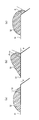
また、上記した濡れピン止め効果について説明すると、図8(a)に示すように、屈曲角αの角部を有する部材31の表面に滴下された溶液32の平衡接触角をθとした場合に、図8(b)に示すように、接触角がθ+αになるまでは溶液32はその角部を通過することができない。それは図8(c)に示すように溶液32が角部を通過した先の斜面では接触角はθより小さくなるからである。すなわち、溶液32の接触角はθ~θ+αの範囲となり、屈曲角αが大なるほど撥液性が高くなることが濡れピン止め効果である。
本発明の有機発光素子及びその製造方法は有機ELディスプレイや有機EL照明装置の発光素子に適用することができる。
11 基板
12,25 バスライン
14 陽極
16 ホール注入・輸送層
18 RG塗布混合層
19 青発光層
20 電子輸送層
21 電子注入層
22 陰極
12,25 バスライン
14 陽極
16 ホール注入・輸送層
18 RG塗布混合層
19 青発光層
20 電子輸送層
21 電子注入層
22 陰極
Claims (7)
- 透明基板と、
前記基板上に並置された金属材料からなるバスライン対と、
前記バスライン対と前記バスライン対のバスライン間の領域とを覆うように形成された透明導電性膜と、
前記透明導電性膜上への有機材料を含む溶液の塗布によって形成された有機材料層と、を含むことを特徴とする有機発光素子。 - 前記有機材料層は陽極としての前記透明導電性膜上に形成されたホール注入・輸送層を含むことを特徴とする請求項1記載の有機発光素子。
- 前記有機材料層は前記ホール注入・輸送層と、前記ホール注入・輸送層上に形成された発光層とを含むことを特徴とする請求項2記載の有機発光素子。
- 前記有機材料を含む溶液はインクジェット法を用いて前記透明導電性膜上に塗布されることを特徴とする請求項1~3のいずれか1記載の有機発光素子。
- 前記バスライン対の並置方向の少なくとも非対向側面が前記基板を臨むように傾斜していることを特徴とする請求項1記載の有機発光素子。
- 前記有機材料層上に電子輸送層、電子注入層及び陰極が順に蒸着により積層されることを特徴とする請求項1~4のいずれか1記載の有機発光素子。
- 透明基板上にバスライン対を並置させるバスライン形成工程と、
前記バスライン対と前記バスライン対のバスライン間の領域とを覆うように透明導電性膜を形成する工程と、
前記透明導電性膜上への有機材料を含む溶液の塗布によって有機材料層を形成する工程と、を含むことを特徴とする有機発光素子の製造方法。
Priority Applications (1)
| Application Number | Priority Date | Filing Date | Title |
|---|---|---|---|
| PCT/JP2011/063381 WO2012169070A1 (ja) | 2011-06-10 | 2011-06-10 | 有機発光素子及びその製造方法 |
Applications Claiming Priority (1)
| Application Number | Priority Date | Filing Date | Title |
|---|---|---|---|
| PCT/JP2011/063381 WO2012169070A1 (ja) | 2011-06-10 | 2011-06-10 | 有機発光素子及びその製造方法 |
Publications (1)
| Publication Number | Publication Date |
|---|---|
| WO2012169070A1 true WO2012169070A1 (ja) | 2012-12-13 |
Family
ID=47295670
Family Applications (1)
| Application Number | Title | Priority Date | Filing Date |
|---|---|---|---|
| PCT/JP2011/063381 Ceased WO2012169070A1 (ja) | 2011-06-10 | 2011-06-10 | 有機発光素子及びその製造方法 |
Country Status (1)
| Country | Link |
|---|---|
| WO (1) | WO2012169070A1 (ja) |
Citations (4)
| Publication number | Priority date | Publication date | Assignee | Title |
|---|---|---|---|---|
| JP2000268980A (ja) * | 1999-03-19 | 2000-09-29 | Toyota Central Res & Dev Lab Inc | 有機電界発光素子 |
| JP2004119216A (ja) * | 2002-09-26 | 2004-04-15 | Fuji Electric Holdings Co Ltd | 有機el発光ディスプレイ |
| JP2007281386A (ja) * | 2006-04-12 | 2007-10-25 | Hitachi Displays Ltd | 有機el表示装置及び有機薄膜デバイス |
| JP2008097845A (ja) * | 2006-10-06 | 2008-04-24 | Sumitomo Chemical Co Ltd | 有機エレクトロルミネッセンス素子 |
-
2011
- 2011-06-10 WO PCT/JP2011/063381 patent/WO2012169070A1/ja not_active Ceased
Patent Citations (4)
| Publication number | Priority date | Publication date | Assignee | Title |
|---|---|---|---|---|
| JP2000268980A (ja) * | 1999-03-19 | 2000-09-29 | Toyota Central Res & Dev Lab Inc | 有機電界発光素子 |
| JP2004119216A (ja) * | 2002-09-26 | 2004-04-15 | Fuji Electric Holdings Co Ltd | 有機el発光ディスプレイ |
| JP2007281386A (ja) * | 2006-04-12 | 2007-10-25 | Hitachi Displays Ltd | 有機el表示装置及び有機薄膜デバイス |
| JP2008097845A (ja) * | 2006-10-06 | 2008-04-24 | Sumitomo Chemical Co Ltd | 有機エレクトロルミネッセンス素子 |
Similar Documents
| Publication | Publication Date | Title |
|---|---|---|
| KR102067376B1 (ko) | 유기 발광 표시 장치 및 그 제조방법 | |
| CN101911831B (zh) | 有机电致发光元件及其制造方法 | |
| JP4526595B2 (ja) | 有機elディスプレイパネル | |
| KR101970539B1 (ko) | 유기전계발광 표시장치 및 이의 제조 방법 | |
| CN104716164A (zh) | 阵列基板及其制作方法、有机发光显示装置 | |
| WO2010109877A1 (ja) | 有機電界発光装置,有機電界発光装置の製造方法,画像表示装置,及び画像表示装置の製造方法 | |
| JP2015207545A (ja) | Oled発光装置及びその製造方法 | |
| US20130234590A1 (en) | Display device and method for manufacturing the same | |
| CN107819079A (zh) | 有机发光显示面板及其制造方法、有机发光显示装置 | |
| JP2008226718A (ja) | 有機el素子 | |
| JP5478954B2 (ja) | 有機エレクトロルミネッセンス表示装置 | |
| CN102845134A (zh) | 转印用施主衬底、器件的制造方法及有机el元件 | |
| US20060238115A1 (en) | Active matrix organic light emitting device and method of manufacturing the same | |
| JP2005174914A (ja) | 有機el装置 | |
| JP4489682B2 (ja) | レーザー熱転写装置,有機電界発光素子の製造方法および有機電界発光素子 | |
| US9917144B2 (en) | Display panel and method for manufacturing same | |
| CN101000948A (zh) | 像素结构及包括该像素结构的有机发光器件 | |
| JP2012209138A (ja) | 有機el素子及びその製造方法、画像表示装置及びその製造方法 | |
| JP4886100B1 (ja) | 有機発光素子及びその製造方法 | |
| JP4752814B2 (ja) | 有機デバイスおよびその製造方法 | |
| WO2013190636A1 (ja) | 有機elパネル | |
| KR20090124156A (ko) | 전기광학소자 및 이의 제작 방법 | |
| JP2009049003A (ja) | 有機el素子 | |
| KR102467214B1 (ko) | 유기발광다이오드표시장치 및 이의 제조방법 | |
| WO2012169070A1 (ja) | 有機発光素子及びその製造方法 |
Legal Events
| Date | Code | Title | Description |
|---|---|---|---|
| 121 | Ep: the epo has been informed by wipo that ep was designated in this application |
Ref document number: 11867526 Country of ref document: EP Kind code of ref document: A1 |
|
| NENP | Non-entry into the national phase |
Ref country code: DE |
|
| 122 | Ep: pct application non-entry in european phase |
Ref document number: 11867526 Country of ref document: EP Kind code of ref document: A1 |
|
| NENP | Non-entry into the national phase |
Ref country code: JP |