WO2012164981A1 - スイッチング電源装置 - Google Patents
スイッチング電源装置 Download PDFInfo
- Publication number
- WO2012164981A1 WO2012164981A1 PCT/JP2012/053919 JP2012053919W WO2012164981A1 WO 2012164981 A1 WO2012164981 A1 WO 2012164981A1 JP 2012053919 W JP2012053919 W JP 2012053919W WO 2012164981 A1 WO2012164981 A1 WO 2012164981A1
- Authority
- WO
- WIPO (PCT)
- Prior art keywords
- switching
- voltage
- circuit
- input voltage
- frequency
- Prior art date
- Legal status (The legal status is an assumption and is not a legal conclusion. Google has not performed a legal analysis and makes no representation as to the accuracy of the status listed.)
- Ceased
Links
Images




Classifications
-
- H—ELECTRICITY
- H02—GENERATION; CONVERSION OR DISTRIBUTION OF ELECTRIC POWER
- H02M—APPARATUS FOR CONVERSION BETWEEN AC AND AC, BETWEEN AC AND DC, OR BETWEEN DC AND DC, AND FOR USE WITH MAINS OR SIMILAR POWER SUPPLY SYSTEMS; CONVERSION OF DC OR AC INPUT POWER INTO SURGE OUTPUT POWER; CONTROL OR REGULATION THEREOF
- H02M1/00—Details of apparatus for conversion
- H02M1/42—Circuits or arrangements for compensating for or adjusting power factor in converters or inverters
- H02M1/4208—Arrangements for improving power factor of AC input
- H02M1/4225—Arrangements for improving power factor of AC input using a non-isolated boost converter
-
- G—PHYSICS
- G05—CONTROLLING; REGULATING
- G05F—SYSTEMS FOR REGULATING ELECTRIC OR MAGNETIC VARIABLES
- G05F1/00—Automatic systems in which deviations of an electric quantity from one or more predetermined values are detected at the output of the system and fed back to a device within the system to restore the detected quantity to its predetermined value or values, i.e. retroactive systems
- G05F1/10—Regulating voltage or current
-
- H—ELECTRICITY
- H02—GENERATION; CONVERSION OR DISTRIBUTION OF ELECTRIC POWER
- H02M—APPARATUS FOR CONVERSION BETWEEN AC AND AC, BETWEEN AC AND DC, OR BETWEEN DC AND DC, AND FOR USE WITH MAINS OR SIMILAR POWER SUPPLY SYSTEMS; CONVERSION OF DC OR AC INPUT POWER INTO SURGE OUTPUT POWER; CONTROL OR REGULATION THEREOF
- H02M1/00—Details of apparatus for conversion
- H02M1/12—Arrangements for reducing harmonics from AC input or output
-
- Y—GENERAL TAGGING OF NEW TECHNOLOGICAL DEVELOPMENTS; GENERAL TAGGING OF CROSS-SECTIONAL TECHNOLOGIES SPANNING OVER SEVERAL SECTIONS OF THE IPC; TECHNICAL SUBJECTS COVERED BY FORMER USPC CROSS-REFERENCE ART COLLECTIONS [XRACs] AND DIGESTS
- Y02—TECHNOLOGIES OR APPLICATIONS FOR MITIGATION OR ADAPTATION AGAINST CLIMATE CHANGE
- Y02B—CLIMATE CHANGE MITIGATION TECHNOLOGIES RELATED TO BUILDINGS, e.g. HOUSING, HOUSE APPLIANCES OR RELATED END-USER APPLICATIONS
- Y02B70/00—Technologies for an efficient end-user side electric power management and consumption
- Y02B70/10—Technologies improving the efficiency by using switched-mode power supplies [SMPS], i.e. efficient power electronics conversion e.g. power factor correction or reduction of losses in power supplies or efficient standby modes
Definitions
- the present invention relates to a switching power supply device that operates so that an input voltage waveform and an input current waveform of a chopper circuit are substantially similar and in phase to improve the power factor.
- Patent Literatures 1 and 2 propose switching power supply devices that improve power factor by performing PFC (Power Factor Correction).
- PFC Power Factor Correction
- switching is performed near the peak and bottom of the input AC power supply voltage (peak in the waveform after full-wave rectification) in order to realize both reduction of switching loss and reduction of conduction noise.
- the frequency is lowered.
- the switching frequency is generally set in a range of 50 kHz to 70 kHz.
- the present invention can achieve both reduction of EMI and good conversion efficiency, and can simplify the input filter provided for EMI reduction.
- the object is to provide a device.
- the present invention relates to a chopper circuit that turns on and off the current to the inductor by a switching element, and a switching control circuit that switches the switching element so that the input voltage waveform and the input current waveform with respect to the phase of the input voltage are substantially similar.
- the switching control circuit switches the switching element at a switching frequency proportional to a term dependent on an input voltage of an expression representing a third harmonic component of a ripple of a current flowing through the inductor. It is configured as described above.
- the switching control circuit is based on an oscillation circuit whose oscillation frequency is controlled by a switching frequency control voltage, the switching frequency of the switching element is defined by the oscillation frequency, an input voltage of the chopper circuit, and an output voltage of the chopper circuit. And an arithmetic circuit for calculating the switching frequency control voltage.
- the switching control circuit may be configured to define a minimum value of the switching frequency.
- the switching frequency is controlled in a form proportional to the term depending on the input voltage of the expression representing the third harmonic component of the current ripple flowing through the inductor. It is possible to suppress both EMI reduction and good conversion efficiency, and to simplify the input filter.
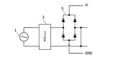
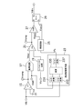
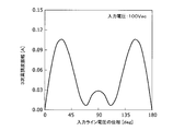
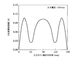
- FIG. 1 is a circuit diagram showing an overall configuration of a switching power supply device according to the present invention. It is a connection diagram of an AC power supply, an input filter, and a full-wave rectifier circuit. It is a block diagram which shows the specific structural example of a control circuit. It is an image figure of a current ripple. It is a graph which shows the relationship between the phase of this input voltage when the input voltage is 100Vac, and the amplitude of the 3rd harmonic component. It is a graph which shows the relationship between the phase of this input voltage when an input voltage is 130Vac, and the amplitude of a 3rd harmonic component. It is a graph which shows the relationship between the phase of this input voltage when the input voltage is 200Vac, and the amplitude of the 3rd harmonic component. It is a graph which shows the relationship between the phase of this input voltage when an input voltage is 230Vac, and the amplitude of a 3rd harmonic component.
- FIG. 1 is a circuit diagram showing the overall configuration of a switching power supply apparatus according to the present invention.
- the input voltage Vi is the output voltage of the full-wave rectifier circuit 5 shown in FIG.
- the input voltage Vi is applied to the smoothing capacitor C2 via the inductor L1 and the diode D1 after high frequency noise is removed by the capacitor C1.
- the DC voltage Vo smoothed by the smoothing capacitor C2 is output from the output terminal of the switching power supply device.
- the current flowing from the inductor L1 to the diode D1 is turned on / off by the switching element Q1 such as a MOSFET connected between the inductor L1 and the diode D1 (when the switching element Q1 is turned on, the diode The current flowing through the diode D1 is turned off by the commutation of the current flowing through the D1 to the switching element Q1.
- the switching element Q1 such as a MOSFET connected between the inductor L1 and the diode D1
- the control unit 7 performs on / off control of the switching element Q1 so that the power factor is improved.
- the control unit 7 includes a control circuit 9, a Vcc detection circuit 11 that detects the voltage Vcc and prevents the control circuit 9 from operating until it exceeds a predetermined value, a drive circuit 13, and complementary connected switching elements QC 1 and QC 2. It has.
- FIG. 3 shows a specific configuration example of the control circuit 9.
- an output voltage error detection circuit 15 comprising an OTA (Operational Transconductance Amplifier) detects an error of the feedback voltage Vfb with respect to the set voltage Vref and outputs an output voltage error signal Vvcmp corresponding to the error. .
- OTA Operaational Transconductance Amplifier
- the output voltage error detection circuit 15 that is OTA outputs a current corresponding to the difference between the set voltage Vref and the feedback voltage Vfb, and integrates the current by the capacitor C4, thereby converting the output voltage error signal Vvcmp into the capacitor C4. It is obtained as a voltage of The voltage Vfb is obtained by dividing the output voltage Vo with voltage dividing resistors R13 and R14 (see FIG. 1). Therefore, the error signal Vvcmp is a signal corresponding to an error with respect to the target value of the output voltage Vo.
- the multiplication circuit 17 executes an operation of multiplying the output voltage error signal Vvcmp by the voltage signal Vdet.
- the voltage signal Vdet is obtained by dividing an input voltage Vi to a chopper circuit including a capacitor C1, an inductor L1, a switching element Q1, a diode D1, and a smoothing capacitor C2 by voltage dividing resistors R11 and R12. is there.
- the input voltage Vi is the output voltage of the full-wave rectifier circuit 5 shown in FIG. Therefore, the waveform of the voltage signal Vdet is a full-wave rectification waveform of the AC voltage from the AC power supply 1 input to the full-wave rectification circuit 5. Therefore, the multiplication circuit 17 generates a current control signal Vmul having an amplitude that is similar to and in phase with the absolute value of the input voltage Vi and is proportional to the output voltage error signal Vvcmp.
- the current flowing through the inductor L1 is converted into a current detection signal Vis by the detection resistor R21. 3 detects the difference between the current detection signal Vis level-shifted by the level shift circuit 19 and the current control signal Vmul, and outputs a signal Vicmp indicating the difference. That is, the current error detection circuit 21 which is an OTA outputs a current corresponding to the difference between the level-shifted current detection signal Vis and the current control signal Vmul, and integrates the current with the capacitor C3, thereby obtaining the signal Vicmp. It is obtained as the voltage of the capacitor C3.
- the signal Vicmp is an average value of the level-shifted current detection signal Vis in the time of about one switching cycle, It is a signal that detects a difference from the current control signal Vmul.
- the comparison circuit 27 compares the signal Vicmp with the output signal Vosc1 (triangular wave or sawtooth wave) of the oscillation circuit 25 whose oscillation frequency is changed by the frequency control voltage Vfs output from the frequency calculation circuit 23. When the former value is exceeded, a reset signal is output to the reset input terminal (R) of the flip-flop 29.
- the output signal Vosc2 of the oscillation circuit 25 is a pulse signal output at the timing when the triangular wave or sawtooth wave, which is the output signal Vosc1, starts to rise, and is applied to the set input terminal (S) of the flip-flop 29 for output.
- the flip-flop 29 is set at the timing when the signal Vosc1 starts to rise.
- the drive circuit 13 shown in FIG. 1 connected to the Q output terminal of the flip-flop 29 turns on the switching elements QC1 and QC2 when the output signal Vdrv of the flip-flop 29 is at a high level (when the flip-flop 29 is set).
- the switching elements QC1 and QC2 are turned off and turned on to turn off the switching element Q1, respectively.
- the switching element Q1 When the flip-flop 29 is set by the output signal Vosc2, the switching element Q1 is turned on.
- the output signal Vosc1 of the oscillation circuit 25 starts increasing, and the value of the signal Vicmp indicating the difference between the value of the current control signal Vmul and the average value of the current detection signal Vis is set.
- the value of the output signal Vosc1 of the oscillation circuit 25 exceeds, a high level signal is input from the comparison circuit 27 to the reset input terminal of the flip-flop 29.
- the switching element Q1 since the Q output terminal of the flip-flop 29 becomes low level, the switching element Q1 is turned off via the drive circuit 13 and the switching elements QC1 and QC2.
- the average value of the current flowing through the inductor L1 in the time of about one switching period is along the waveform of the current control signal Vmul that is similar to (proportional to) the full-wave rectified waveform of the AC voltage from the AC power supply 1. It will change.
- the signal Vicmp increases, thereby increasing the on-time of the switching element Q and increasing the average value of the current flowing through the inductor L1.
- the signal Vicmp becomes small, the ON time of the switching element Q1 is shortened, and the average value of the current flowing through the inductor L1 decreases. In this way, a similar current in phase with the input voltage signal Vin flows through the inductor L1, and as a result, the power factor is improved.
- the switching frequency is generally set in a range of 50 kHz to 70 kHz. Since the switching power supply generates EMI, an input filter 3 as shown in FIG. 2 is generally interposed between the AC power supply 1 and the rectifier circuit 5 in order to clear the EMI-related standard. I am doing so.
- the input filter 3 acts to suppress switching noise from entering the external AC line, and generally exhibits a characteristic that the attenuation rate increases as the frequency increases.
- the standard for the frequency of switching noise is 150 kHz or more. Accordingly, in the frequency band of about 150 kHz to 1 MHz considering third harmonics, setting the switching frequency to 65 kHz is more advantageous for simplifying the input filter than setting the switching frequency to 55 kHz. If the switching frequency is increased to about 75 kHz, another inconvenience (such as deterioration in conversion efficiency due to an increase in switching loss) occurs. For the above reasons, the switching frequency is often set to about 65 kHz.
- the bottleneck in suppressing EMI is normal noise which is a kind of conduction noise. Since the standard for the frequency of conduction noise is 150 kHz to 30 MHz, the fundamental component and the second harmonic component are out of the standard for the switching frequency of 50 kHz to 70 kHz. Therefore, the maximum value of the normal noise is determined by the third harmonic component of the current ripple flowing in the inductor L1 shown in FIG. In other words, if the third harmonic component of the current ripple flowing through the inductor L1 is suppressed, EMI can be suppressed, and as a result, the input filter 3 (EMI filter) can be simplified. .
- FIG. 4 is an image diagram of the current ripple. This current ripple is given by the following equation (1).
- Vac is the effective value of the AC input voltage
- ⁇ is the phase of the AC input voltage
- L is the inductance of the inductor L1
- Fs is the switching frequency
- D is the duty (duty ratio or on-time ratio) of the switching cycle, and is given by the following equation (2).
- Vo is an output voltage.
- the third harmonic component shown in the following formula (3) is obtained by Fourier transforming the current ripple ⁇ I.
- the Fourier transform one triangular wave indicated by a solid line in FIG. 4 is taken out and is converted.
- the current ripple ⁇ I to be converted is obtained by substituting D in Expression (2) into Expression (1).
- the period is 1 / Fs, and the peak position in the triangular wave is determined using the duty.
- the phase ⁇ is treated as a constant, and this ⁇ is changed as a parameter in later analysis.
- the level of the third harmonic component is inversely proportional to the switching frequency Fs, and is affected by the effective value Vac of the AC input voltage and the phase ⁇ .
- equation (3) indicates that the maximum value of the third harmonic component is not related to the input voltage.
- the peak value of the third harmonic component is about 30 ° of the phase of this input voltage. And at 150 °.
- the peak values are at about 20 °, 90 °, and 160 ° of the same phase. Also, as shown in FIG.
- the peak values are at the same phase of about 15 °, 45 °, 135 °, and 165 °. Furthermore, as shown in FIG. 8, when the AC input voltage is 230 Vac, the peak value is in the region of about 10 °, 30 °, and 90 ° in the same phase, 150 ° and 170 °. As described above, the phase of the AC input voltage at which the third-order harmonic component reaches a peak differs greatly depending on the effective value of the input voltage.
- the switching frequency is controlled so that the third harmonic component can be suppressed regardless of the value of the input voltage.
- the switching frequency Fs is expressed by an equation (3) representing the third harmonic component of the current ripple so that the equation (3) does not depend on the input voltage. Control may be performed in proportion to the term depending on the input voltage in 3). Then, limiting the minimum switching frequency is also executed.
- the minimum switching frequency Fsmin may be set and the switching frequency Fs may be controlled based on the relationship of the following expression (4).
- Fsmax represents the maximum value of the switching frequency Fs.
- the frequency control voltage Vfs output from the frequency calculation circuit 23 in FIG. 3 and the oscillation frequency Fs of the oscillation circuit 25 have the following relationship.
- Ks is a constant.
- the input voltage Vi and the AC input voltage Vac shown in FIG. (Strictly speaking, the absolute value of the right-hand side of equation (6) is Vi, but the following discussion holds true.)
- the frequency control voltage Vfs for setting the oscillation frequency Fs of the oscillation circuit 25 to the maximum frequency and the minimum frequency is set as Vfsmax and Vfsmin, respectively
- the frequency control voltage Vfs is expressed by the following equation using equations (4) to (6). It is expressed as (7).
- the relationship between the input voltage Vi and the monitor voltage Vdet related to the voltage Vi is as follows.
- the relationship between the output voltage Vo and the monitor voltage Vfb related to the voltage Vo is expressed as follows.
- the constants Mi and Mo are determined by the resistance voltage division ratio.
- the said Formula (7) is represented as follows using the relationship of Formula (8) and (9).
- the calculation unit 235 of the frequency calculation circuit 23 shown in FIG. 3 takes in the monitor voltage Vdet related to the input voltage Vi through the A / D converter 231 and also acquires the monitor voltage Vfb related to the output voltage Vo to the A / D converter. 234, and the calculation of the above formula (10) is executed. Then, the frequency control voltage Vfs obtained by the calculation is output to the oscillation circuit 25 via the D / A converter 237.
- the switching power supply according to the present embodiment that controls the oscillation frequency of the oscillation circuit 25 by the frequency control voltage Vfs determined by the above equation (10) the third harmonic component of the current ripple whose switching frequency flows through the inductor L1.
- the minimum switching frequency Fsmin is provided because the switching frequency can be reduced to zero unless the minimum switching frequency is set. If the switching frequency is lowered, problems such as increase in required inductors and smoothing capacitors and increase in output ripple occur. Therefore, it is important to set a lower limit of the switching frequency.
Landscapes
- Engineering & Computer Science (AREA)
- Power Engineering (AREA)
- Physics & Mathematics (AREA)
- Electromagnetism (AREA)
- General Physics & Mathematics (AREA)
- Radar, Positioning & Navigation (AREA)
- Automation & Control Theory (AREA)
- Dc-Dc Converters (AREA)
- Rectifiers (AREA)
Abstract
Description
この特許文献1、2に係るスイッチング電源装置では、スイッチング損失の低減と伝導ノイズの低減の双方を実現するため、入力交流電源電圧のピークとボトム(全波整流後の波形ではピーク)付近においてスイッチング周波数を下げるようにしている。
なお、スイッチング電源装置では、一般的にスイッチング周波数が50kHz~70kHzの範囲に設定される。
すなわち、EMIを抑制する上でのボトルネックは、伝導ノイズの一種であるノーマルノイズである。伝導ノイズの周波数の規格は、150kHz~30MHzであるため、50kHz~70kHzのスイッチング周波数にとって、その基本成分と二次高調波成分は規格外となる。したがって、このノーマルノイズの最大値は、インダクタに流れている電流リップルの3次高調波成分で決まることになる。しかし、特許文献1、2に係る制御方式では、3次高調波成分に適応できないため、EMIの低減と良好な変換効率とを両立し得ないことがある。
また、前記スイッチング制御回路は、前記スイッチング周波数の最小値を規定するように構成することができる。
このスイッチング電源装置において、入力電圧Viは、図2に示す全波整流回路5の出力電圧である。この入力電圧Viは、キャパシタC1により高周波ノイズを除去された後、インダクタL1とダイオードD1を介して平滑キャパシタC2に印加される。その結果、このスイッチング電源装置の出力端子からは、平滑キャパシタC2によって平滑化された直流電圧Voが出力される。
一方、このスイッチング電源装置においては、インダクタL1とダイオードD1の間に接続されたMOSFETなどのスイッチング素子Q1によってインダクタL1からダイオードD1に流れる電流がオン・オフされる(スイッチング素子Q1がオンすると、ダイオードD1に流れる電流がスイッチング素子Q1に転流されることにより、ダイオードD1に流れる電流がオフされる。)。
図3に制御回路9の具体的な構成例を示す。図3において、OTA(Operational Transconductance Amplifier)からなる出力電圧誤差検出回路15は、設定電圧Vrefに対するフィードバック電圧Vfbの誤差を検出して、その誤差に対応する信号である出力電圧誤差信号Vvcmpを出力する。すなわち、OTAである出力電圧誤差検出回路15は、設定電圧Vrefとフィードバック電圧Vfbとの差に応じた電流を出力し、その電流をキャパシタC4で積分することにより、出力電圧誤差信号VvcmpをキャパシタC4の電圧として得るのである。電圧Vfbは、上記出力電圧Voを分圧抵抗R13、R14(図1参照)で分圧したものである。従って、誤差信号Vvcmpは、上記出力電圧Voの目標値に対する誤差に対応する信号である。
ここで、キャパシタC3を含めた電流検出誤差検出回路21の応答をある程度遅くしてあるので、信号Vicmpは、レベルシフトされた電流検出信号Visのスイッチング周期1周期分程度の時間における平均値と、電流制御信号Vmulとの差を検出した信号となっている。
比較回路27は、信号Vicmpと、周波数演算回路23から出力される周波数制御電圧Vfsによって発振周波数が変化される発振回路25の出力信号Vosc1(三角波もしくは鋸波)とを比較し、後者の値が前者の値を超えるときにフリップフロップ29のリセット入力端子(R)にリセット信号を出力する。一方、発振回路25の出力信号Vosc2は、出力信号Vosc1である三角波もしくは鋸波が上昇を開始するタイミングで出力されるパルス信号であり、フリップフロップ29のセット入力端子(S)に加えられ、出力信号Vosc1が上昇を開始するタイミングでフリップフロップ29をセットする。
スイッチングノイズの周波数についての規格は150kHz以上である。従って、3次高調波を考慮した150kHz~1MHzくらいの周波数帯域では、スイッチング周波数を55kHzに設定するよりも、65kHzに設定する方が入力フィルタの簡素化を図る上で有利になる。なお、スイッチング周波数を75kHz程度まで高くすると、別の不都合(スイッチング損失の増大による変換効率の悪化等)が発生することになる。以上の理由から、スイッチング周波数は65kHz程度に設定することが多い。

ここで、Vacは交流入力電圧の実効値、θは交流入力電圧の位相、LはインダクタL1のインダクタンス、Fsはスイッチング周波数をそれぞれ表す。Dはスイッチングサイクルのデューティ(時比率、もしくはオン時比率)であり、下式(2)によって与えられる。

ここで、Voは出力電圧である。

フーリエ変換は、図4に実線で示される三角波をひとつ取り出し、それを変換対象とする。このとき、変換する電流リップル△Iには、式(1)に式(2)のDを代入したものを用いる。また、周期は1/Fsを用い、三角波中のピークの位置はデューティを用いて決めている。フーリエ変換を行っているとき、位相θは定数として扱い、あとの解析でこのθをパラメータとして変化させる。
式(3)から明らかなように、3次高調波成分のレベルはスイッチング周波数Fsに反比例し、また、交流入力電圧の実効値Vacと位相θの影響を受ける。さらに、式(3)は、3次高調波成分の最大値が入力電圧と関係しないことを示している。
また、図6に示すように、交流入力電圧が130Vである場合には、同ピーク値が同位相の約20°、90°、160°にある。また、図7に示すように、交流入力電圧が200Vacである場合には、同ピーク値が同位相の約15°、45°、135°、165°にある。
さらに、図8に示すように、交流入力電圧が230Vacの場合には、同ピーク値が同位相の約10°、30°、90°を中心とする領域、150°170°にある。このように、3次高調波成分がピークになる交流入力電圧の位相は該入力電圧の実効値によって大きく相違する。
したがって、交流入力電圧が100Vacのときには、EMIの低減と変換効率を両立できるものの、交流入力電圧が130Vacと230Vacの場合では、位相90°付近において、スイッチング周波数が低くなっているのにもかかわらず3次高調波成分が大きいため、EMIを抑えきれないおそれがある。交流入力電圧が200Vacの場合も、同様の傾向がある。したがって、特許文献1、2の制御方式では、交流入力電圧の大きさによってEMIの低減と変換効率とを両立できないという状態が発生する。
入力電圧の値によらず3次高調波成分を抑制するためには、式(3)が入力電圧に依存しない形になるよう、スイッチング周波数Fsを電流リップルの3次高調波成分を表す式(3)の入力電圧に依存する項に比例するように制御すればよい。そして、最小スイッチング周波数を制限することを合わせて実行する。
例えば、最小スイッチング周波数Fsminを設定し、スイッチング周波数Fsを下式(4)の関係に基づいて制御すればよい。

ここで、Fsmaxはスイッチング周波数Fsの最大値を表す。式(4)のFsを式(3)に代入することにより、3次高調波成分が、基本的に交流入力電圧の実効値Vacおよび交流入力電圧の位相θに依存しないものになることが分かる。

ここで、Ksは定数である。
また、図1に示す入力電圧Viと交流入力電圧Vacには以下の関係がある。(厳密にいえば、式(6)の右辺の絶対値がViとなるが、以下の議論は同様に成立する。)


入力電圧Viと該電圧Viに係るモニター電圧Vdetとの関係は以下のようになる。

また、出力電圧Voと該電圧Voに係るモニター電圧Vfbとの関係は以下のように表される。

ここで、定数MiとMoは抵抗分圧比で決定される。
そして、上記式(7)は、式(8)と(9)の関係を用いて以下のように表される。

上記式(10)によって決定される周波数制御電圧Vfsによって発振回路25の発振周波数を制御する本実施形態に係るスイッチング電源装置によれば、スイッチング周波数がインダクタL1を流れる電流リップルの3次高調波成分を表す式の入力電圧に依存する項に比例する形態で制御されることになるので、この3次高調波成分を抑制してEMIの低減と変換効率を両立することができるとともに、フィルタ3の簡素化を図ることが可能になる。なお、最小スイッチング周波数Fsminを設けるのは、最小スイッチング周波数を設定しないと、スイッチング周波数がゼロまで下がりうることになってしまうからである。スイッチング周波数が低くなると、必要なインダクタや平滑コンデンサが大きくなってしまう、出力のリップルが大きくなってしまう、などの問題が生じるため、スイッチング周波数の下限を設けることは重要である。
3 入力フィルタ
5 全波整流回路
7 制御部
9 制御回路
11 Vcc検出回路
13 ドライブ回路
15 出力電圧誤差検出回路
17 乗算回路
19 レベルシフト回路
21 電流誤差検出回路
23 周波数演算回路
231,233 A/D変換器
235 演算部
237 D/A変換器
25 発振回路
27 比較回路
29 フリップフロップ
L1 インダクタ
D1 ダイオード
Q1 スイッチング素子
C1,C2,C3,C4 キャパシタ
R11~R13 分圧抵抗
R21 検出抵抗
Claims (3)
- インダクタへの通電をスイッチング素子によってオン・オフするチョッパ回路と、入力電圧の位相に対する入力電圧波形と入力電流波形がほぼ相似形となるように前記スイッチング素子をスイッチングさせるスイッチング制御回路とを備えるスイッチング電源装置であって、
前記スイッチング制御回路は、前記インダクタに流れる電流のリップルの3次高調波成分を表す式の入力電圧に依存する項に比例するスイッチング周波数で前記スイッチング素子をスイッチングさせるように構成されていることを特徴とするスイッチング電源装置。 - 前記スイッチング制御回路は、
スイッチング周波数制御電圧によって発振周波数が制御され、その発振周波数によって前記スイッチング素子のスイッチング周波数を規定する発振回路と、
前記チョッパ回路の入力電圧と前記チョッパ回路の出力電圧とに基づいて、前記スイッチング周波数制御電圧を演算する演算回路と、
を備えることを特徴とする請求項1に記載のスイッチング電源装置。 - 前記スイッチング制御回路は、前記スイッチング周波数の最小値を規定するように構成されていることを特徴とする請求項1に記載のスイッチング電源装置。
Priority Applications (2)
| Application Number | Priority Date | Filing Date | Title |
|---|---|---|---|
| US13/695,860 US8878506B2 (en) | 2011-06-02 | 2012-02-20 | Switching power supply device |
| JP2012550228A JP5423906B2 (ja) | 2011-06-02 | 2012-02-20 | スイッチング電源装置 |
Applications Claiming Priority (2)
| Application Number | Priority Date | Filing Date | Title |
|---|---|---|---|
| JP2011124133 | 2011-06-02 | ||
| JP2011-124133 | 2011-06-02 |
Publications (1)
| Publication Number | Publication Date |
|---|---|
| WO2012164981A1 true WO2012164981A1 (ja) | 2012-12-06 |
Family
ID=47258849
Family Applications (1)
| Application Number | Title | Priority Date | Filing Date |
|---|---|---|---|
| PCT/JP2012/053919 Ceased WO2012164981A1 (ja) | 2011-06-02 | 2012-02-20 | スイッチング電源装置 |
Country Status (3)
| Country | Link |
|---|---|
| US (1) | US8878506B2 (ja) |
| JP (1) | JP5423906B2 (ja) |
| WO (1) | WO2012164981A1 (ja) |
Cited By (1)
| Publication number | Priority date | Publication date | Assignee | Title |
|---|---|---|---|---|
| JP2021151121A (ja) * | 2020-03-19 | 2021-09-27 | 新電元工業株式会社 | 制御装置及びそれを有する電力変換装置 |
Families Citing this family (2)
| Publication number | Priority date | Publication date | Assignee | Title |
|---|---|---|---|---|
| US9837893B2 (en) * | 2013-07-31 | 2017-12-05 | Fairchild Korea Semiconductor Ltd. | Charge pump and switch control circuit |
| CN105191104A (zh) * | 2013-10-01 | 2015-12-23 | 富士电机株式会社 | 功率因数改善电路 |
Citations (2)
| Publication number | Priority date | Publication date | Assignee | Title |
|---|---|---|---|---|
| JP2008005682A (ja) * | 2006-06-26 | 2008-01-10 | Densei Lambda Kk | パルス制御装置 |
| JP2010233439A (ja) * | 2009-03-03 | 2010-10-14 | Toshiba Corp | 電源制御装置、及びそれを用いた電源装置 |
Family Cites Families (6)
| Publication number | Priority date | Publication date | Assignee | Title |
|---|---|---|---|---|
| US5734562A (en) * | 1994-06-20 | 1998-03-31 | Redl; Richard | Power factor correction circuit |
| US8054056B2 (en) * | 2006-09-16 | 2011-11-08 | Texas Instruments Incorporated | Frequency regulated hysteretic average current mode converter |
| US8723438B2 (en) * | 2007-03-12 | 2014-05-13 | Cirrus Logic, Inc. | Switch power converter control with spread spectrum based electromagnetic interference reduction |
| JP5347637B2 (ja) | 2009-03-27 | 2013-11-20 | 富士電機株式会社 | スイッチング電源 |
| JP5347710B2 (ja) | 2009-05-20 | 2013-11-20 | 富士電機株式会社 | スイッチング電源 |
| EP2360824B1 (en) * | 2009-12-31 | 2015-08-26 | Nxp B.V. | Controller for a power conversion circuit |
-
2012
- 2012-02-20 US US13/695,860 patent/US8878506B2/en active Active
- 2012-02-20 WO PCT/JP2012/053919 patent/WO2012164981A1/ja not_active Ceased
- 2012-02-20 JP JP2012550228A patent/JP5423906B2/ja active Active
Patent Citations (2)
| Publication number | Priority date | Publication date | Assignee | Title |
|---|---|---|---|---|
| JP2008005682A (ja) * | 2006-06-26 | 2008-01-10 | Densei Lambda Kk | パルス制御装置 |
| JP2010233439A (ja) * | 2009-03-03 | 2010-10-14 | Toshiba Corp | 電源制御装置、及びそれを用いた電源装置 |
Cited By (2)
| Publication number | Priority date | Publication date | Assignee | Title |
|---|---|---|---|---|
| JP2021151121A (ja) * | 2020-03-19 | 2021-09-27 | 新電元工業株式会社 | 制御装置及びそれを有する電力変換装置 |
| JP7355686B2 (ja) | 2020-03-19 | 2023-10-03 | 新電元工業株式会社 | 制御装置及びそれを有する電力変換装置 |
Also Published As
| Publication number | Publication date |
|---|---|
| JP5423906B2 (ja) | 2014-02-19 |
| JPWO2012164981A1 (ja) | 2015-02-23 |
| US20130127432A1 (en) | 2013-05-23 |
| US8878506B2 (en) | 2014-11-04 |
Similar Documents
| Publication | Publication Date | Title |
|---|---|---|
| CN102484425B (zh) | Pfc转换器 | |
| US10396655B2 (en) | Power factor correction circuit, control method and controller | |
| JP5136364B2 (ja) | 力率改善回路の制御方式 | |
| JP5182375B2 (ja) | Pfcコンバータ | |
| JP5104946B2 (ja) | Pfcコンバータ | |
| JP5141774B2 (ja) | Pfcコンバータ | |
| JP5273158B2 (ja) | Pfcコンバータ | |
| JP5170096B2 (ja) | Pfcコンバータ | |
| JP6217340B2 (ja) | 電源装置 | |
| CN102308462B (zh) | 开关电源装置 | |
| JP5326804B2 (ja) | 力率改善電源装置、該電源装置に用いられる制御回路および制御方法 | |
| EP2360824B1 (en) | Controller for a power conversion circuit | |
| JP6075462B2 (ja) | 力率改善回路 | |
| US20110317459A1 (en) | Controller for a power conversion circuit | |
| JP5282660B2 (ja) | スイッチング電源 | |
| CN106877644A (zh) | 开关电源装置 | |
| JP5423906B2 (ja) | スイッチング電源装置 | |
| JP2011155813A (ja) | Pfcコンバータの制御回路、制御方法、および電源装置 |
Legal Events
| Date | Code | Title | Description |
|---|---|---|---|
| ENP | Entry into the national phase |
Ref document number: 2012550228 Country of ref document: JP Kind code of ref document: A |
|
| WWE | Wipo information: entry into national phase |
Ref document number: 13695860 Country of ref document: US |
|
| 121 | Ep: the epo has been informed by wipo that ep was designated in this application |
Ref document number: 12792154 Country of ref document: EP Kind code of ref document: A1 |
|
| NENP | Non-entry into the national phase |
Ref country code: DE |
|
| 122 | Ep: pct application non-entry in european phase |
Ref document number: 12792154 Country of ref document: EP Kind code of ref document: A1 |