WO2012164847A1 - 化合物半導体基板、及びその製造方法、並びにその化合物半導体基板を用いた発光素子 - Google Patents
化合物半導体基板、及びその製造方法、並びにその化合物半導体基板を用いた発光素子 Download PDFInfo
- Publication number
- WO2012164847A1 WO2012164847A1 PCT/JP2012/003192 JP2012003192W WO2012164847A1 WO 2012164847 A1 WO2012164847 A1 WO 2012164847A1 JP 2012003192 W JP2012003192 W JP 2012003192W WO 2012164847 A1 WO2012164847 A1 WO 2012164847A1
- Authority
- WO
- WIPO (PCT)
- Prior art keywords
- layer
- light emitting
- semiconductor substrate
- compound semiconductor
- cladding layer
- Prior art date
- Legal status (The legal status is an assumption and is not a legal conclusion. Google has not performed a legal analysis and makes no representation as to the accuracy of the status listed.)
- Ceased
Links
Images


Classifications
-
- H—ELECTRICITY
- H10—SEMICONDUCTOR DEVICES; ELECTRIC SOLID-STATE DEVICES NOT OTHERWISE PROVIDED FOR
- H10H—INORGANIC LIGHT-EMITTING SEMICONDUCTOR DEVICES HAVING POTENTIAL BARRIERS
- H10H20/00—Individual inorganic light-emitting semiconductor devices having potential barriers, e.g. light-emitting diodes [LED]
- H10H20/80—Constructional details
- H10H20/81—Bodies
- H10H20/822—Materials of the light-emitting regions
- H10H20/824—Materials of the light-emitting regions comprising only Group III-V materials, e.g. GaP
-
- H—ELECTRICITY
- H10—SEMICONDUCTOR DEVICES; ELECTRIC SOLID-STATE DEVICES NOT OTHERWISE PROVIDED FOR
- H10P—GENERIC PROCESSES OR APPARATUS FOR THE MANUFACTURE OR TREATMENT OF DEVICES COVERED BY CLASS H10
- H10P14/00—Formation of materials, e.g. in the shape of layers or pillars
- H10P14/20—Formation of materials, e.g. in the shape of layers or pillars of semiconductor materials
- H10P14/24—Formation of materials, e.g. in the shape of layers or pillars of semiconductor materials using chemical vapour deposition [CVD]
-
- H—ELECTRICITY
- H10—SEMICONDUCTOR DEVICES; ELECTRIC SOLID-STATE DEVICES NOT OTHERWISE PROVIDED FOR
- H10P—GENERIC PROCESSES OR APPARATUS FOR THE MANUFACTURE OR TREATMENT OF DEVICES COVERED BY CLASS H10
- H10P14/00—Formation of materials, e.g. in the shape of layers or pillars
- H10P14/20—Formation of materials, e.g. in the shape of layers or pillars of semiconductor materials
- H10P14/29—Formation of materials, e.g. in the shape of layers or pillars of semiconductor materials characterised by the substrates
- H10P14/2901—Materials
- H10P14/2907—Materials being Group IIIA-VA materials
- H10P14/2911—Arsenides
-
- H—ELECTRICITY
- H10—SEMICONDUCTOR DEVICES; ELECTRIC SOLID-STATE DEVICES NOT OTHERWISE PROVIDED FOR
- H10P—GENERIC PROCESSES OR APPARATUS FOR THE MANUFACTURE OR TREATMENT OF DEVICES COVERED BY CLASS H10
- H10P14/00—Formation of materials, e.g. in the shape of layers or pillars
- H10P14/20—Formation of materials, e.g. in the shape of layers or pillars of semiconductor materials
- H10P14/32—Formation of materials, e.g. in the shape of layers or pillars of semiconductor materials characterised by intermediate layers between substrates and deposited layers
- H10P14/3202—Materials thereof
- H10P14/3214—Materials thereof being Group IIIA-VA semiconductors
- H10P14/3218—Phosphides
-
- H—ELECTRICITY
- H10—SEMICONDUCTOR DEVICES; ELECTRIC SOLID-STATE DEVICES NOT OTHERWISE PROVIDED FOR
- H10P—GENERIC PROCESSES OR APPARATUS FOR THE MANUFACTURE OR TREATMENT OF DEVICES COVERED BY CLASS H10
- H10P14/00—Formation of materials, e.g. in the shape of layers or pillars
- H10P14/20—Formation of materials, e.g. in the shape of layers or pillars of semiconductor materials
- H10P14/32—Formation of materials, e.g. in the shape of layers or pillars of semiconductor materials characterised by intermediate layers between substrates and deposited layers
- H10P14/3202—Materials thereof
- H10P14/3214—Materials thereof being Group IIIA-VA semiconductors
- H10P14/3221—Arsenides
-
- H—ELECTRICITY
- H10—SEMICONDUCTOR DEVICES; ELECTRIC SOLID-STATE DEVICES NOT OTHERWISE PROVIDED FOR
- H10P—GENERIC PROCESSES OR APPARATUS FOR THE MANUFACTURE OR TREATMENT OF DEVICES COVERED BY CLASS H10
- H10P14/00—Formation of materials, e.g. in the shape of layers or pillars
- H10P14/20—Formation of materials, e.g. in the shape of layers or pillars of semiconductor materials
- H10P14/32—Formation of materials, e.g. in the shape of layers or pillars of semiconductor materials characterised by intermediate layers between substrates and deposited layers
- H10P14/3242—Structure
- H10P14/3244—Layer structure
- H10P14/3248—Layer structure consisting of two layers
-
- H—ELECTRICITY
- H10—SEMICONDUCTOR DEVICES; ELECTRIC SOLID-STATE DEVICES NOT OTHERWISE PROVIDED FOR
- H10P—GENERIC PROCESSES OR APPARATUS FOR THE MANUFACTURE OR TREATMENT OF DEVICES COVERED BY CLASS H10
- H10P14/00—Formation of materials, e.g. in the shape of layers or pillars
- H10P14/20—Formation of materials, e.g. in the shape of layers or pillars of semiconductor materials
- H10P14/34—Deposited materials, e.g. layers
- H10P14/3402—Deposited materials, e.g. layers characterised by the chemical composition
- H10P14/3414—Deposited materials, e.g. layers characterised by the chemical composition being group IIIA-VIA materials
- H10P14/3418—Phosphides
-
- H—ELECTRICITY
- H10—SEMICONDUCTOR DEVICES; ELECTRIC SOLID-STATE DEVICES NOT OTHERWISE PROVIDED FOR
- H10P—GENERIC PROCESSES OR APPARATUS FOR THE MANUFACTURE OR TREATMENT OF DEVICES COVERED BY CLASS H10
- H10P14/00—Formation of materials, e.g. in the shape of layers or pillars
- H10P14/20—Formation of materials, e.g. in the shape of layers or pillars of semiconductor materials
- H10P14/34—Deposited materials, e.g. layers
- H10P14/3438—Doping during depositing
- H10P14/3441—Conductivity type
- H10P14/3444—P-type
-
- H—ELECTRICITY
- H10—SEMICONDUCTOR DEVICES; ELECTRIC SOLID-STATE DEVICES NOT OTHERWISE PROVIDED FOR
- H10H—INORGANIC LIGHT-EMITTING SEMICONDUCTOR DEVICES HAVING POTENTIAL BARRIERS
- H10H20/00—Individual inorganic light-emitting semiconductor devices having potential barriers, e.g. light-emitting diodes [LED]
- H10H20/80—Constructional details
- H10H20/81—Bodies
- H10H20/817—Bodies characterised by the crystal structures or orientations, e.g. polycrystalline, amorphous or porous
Definitions
- the present invention relates to a compound semiconductor substrate, a manufacturing method thereof, and a light-emitting element using the compound semiconductor substrate.
- AlGaInP Al x Ga 1-x
- AlGaInP Al x Ga 1-x
- a light-emitting layer made of a quaternary mixed crystal A material manufactured from a compound semiconductor substrate obtained by epitaxial growth of a light-emitting layer made of a quaternary mixed crystal is often used.
- Patent Document 1 when AlGaInP is epitaxially grown, the difference ⁇ between the Bragg angles of the lattice planes (400) of AlGaInP and GaAs is 0 ′′ to a low angle.
- a method of forming a light emitting layer by adjusting the composition of AlGaInP by matching the lattice constants of AlGaInP and GaAs has been performed.
- the lattice constant of the epitaxially grown AlGaInP layer can be changed to the lattice constant of GaAs by forming a layer whose mixed crystal ratio gradually changes from GaAs to the lattice constant of AlGaInP or by forming a layer that relaxes mismatch. An attempt was made to bring it closer to.
- the lattice constants of AlGaInP and GaAs are matched so that the difference ⁇ between the Bragg angles of the lattice planes (400) of AlGaInP and GaAs becomes 0 ′′ to a low angle.
- dislocations are easily propagated to the light emitting layer, so that deterioration of the light emitting life characteristics of the entire compound semiconductor substrate and variations in the light emitting life characteristics in the surface of the compound semiconductor substrate occur. Also, it was found that the degree of deterioration and variation becomes unstable between batches.
- the present invention has been made in order to solve the above problems, and by suppressing the propagation of dislocations to the light emitting layer, the light emission life characteristics are increased, and the in-plane variation of the light emission life characteristics is improved. It is an object of the present invention to provide a high-quality compound semiconductor substrate with improved luminance and a method for manufacturing the same. Furthermore, an object of the present invention is to provide a light emitting device using the compound semiconductor substrate.
- a lower cladding layer represented by (Al x Ga 1-x ) y In 1-y P (where 0 ⁇ x ⁇ 1, 0 ⁇ y ⁇ 1), an active layer, And a compound semiconductor substrate having a light emitting layer having a double hetero structure of an upper cladding layer and having a first GaP window layer on the light emitting layer, A difference ⁇ between the Bragg angle at the (400) plane of the lower cladding layer, the active layer, and the upper cladding layer and the (400) plane of the GaAs single crystal (hereinafter, simply referred to as ⁇ ). ) Having a lattice constant of the lower clad layer, the active layer, and the upper clad layer so as to be 50 ′′ to 200 ′′ at room temperature, respectively. .
- each layer of the compound semiconductor substrate is a compound semiconductor substrate so long as the lattice constants of the lower cladding layer, the active layer, and the upper cladding layer are matched so that ⁇ is 50 ′′ to 200 ′′ at room temperature. Stress relaxation effectively works, and dislocations such as misfit dislocations are suppressed from propagating to each layer of the light emitting layer, so that the light emission life characteristics are increased, and the variation in the light emission life characteristics is improved.
- the compound semiconductor substrate has improved luminance.
- the lattice constants of the lower cladding layer, the active layer, and the upper cladding layer are matched so that ⁇ is 50 ′′ to 150 ′′, particularly 50 ′′ to 100 ′′, at room temperature.
- the stress relaxation between the layers of the compound semiconductor substrate works more effectively, and the propagation of dislocations such as misfit dislocations to the light emitting layers is suppressed, so that further emission
- the lifetime characteristics are increased, the in-plane variation of the emission lifetime characteristics is improved, and the compound semiconductor substrate is further improved in luminance.
- the present invention provides a light-emitting element manufactured from the compound semiconductor substrate.
- the light emitting lifetime characteristics are increased, the variation in the light emitting lifetime characteristics among the light emitting elements is improved, and the luminance is further improved.
- a lower cladding layer represented by (Al x Ga 1-x ) y In 1-y P (where 0 ⁇ x ⁇ 1, 0 ⁇ y ⁇ 1), an active layer, And a light emitting layer growth step of epitaxially growing a light emitting layer comprising a double hetero structure of the upper cladding layer, A first GaP window layer growth step of epitaxially growing a first GaP window layer on the light emitting layer; Etching to remove the GaAs substrate and expose the lower cladding layer; A second GaP window layer forming step of forming a second GaP window layer on the exposed lower cladding layer, comprising: In the light emitting layer growth step, the difference ⁇ between the Bragg angle at the (400) plane of the lower cladding layer, the active layer, and the upper cladding layer and the Bragg angle at the (400) plane of the GaAs substrate is at room temperature, respectively.
- a method of manufacturing a compound semiconductor substrate characterized in that the light emitting
- the manufacturing method of the compound semiconductor substrate having such a light emitting layer growth step stress relaxation between each layer of the compound semiconductor substrate works effectively during manufacturing, and dislocation such as misfit dislocation propagates to each layer of the light emitting layer. Therefore, it is possible to manufacture a compound semiconductor substrate in which the emission lifetime characteristics are increased, the in-plane variation of the emission lifetime characteristics is improved, and the luminance is further improved.
- the ⁇ is 50 ′′ to 150 ′′, particularly 50 ′′ to 100 ′′, respectively, at room temperature.
- the difference ⁇ between the Bragg angle in the (400) plane of the lower cladding layer, the active layer, and the upper cladding layer and the Bragg angle in the (400) plane of the GaAs single crystal is 50 ′′ to 200 at room temperature, respectively.
- the lattice constants of the lower cladding layer, the active layer, and the upper cladding layer are matched so that the stress between the layers of the compound semiconductor substrate is relaxed, misfit dislocation, etc. Since propagation of dislocations to each layer of the light emitting layer is suppressed, the light emission lifetime characteristics are increased, the in-plane variation of the light emission lifetime characteristics is improved, and the compound semiconductor substrate is further improved in luminance.
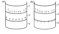
- FIG. 5 is a diagram showing the dislocation propagation direction
- substrate It is the figure which showed the propagation direction of the dislocation accompanying internal stress in the schematic sectional drawing of a board
- substrate
- the present inventors have found that the Bragg angle at the (400) plane of the lower cladding layer, the active layer, and the upper cladding layer and the Bragg angle at the (400) plane of the GaAs single crystal.
- the compound semiconductor substrate has the lattice constants of the lower cladding layer, the active layer, and the upper cladding layer matched so that the difference ⁇ between them is 50 ′′ to 200 ′′ at room temperature, the stress between each layer of the compound semiconductor substrate It is found that the propagation of dislocations such as misfit dislocations to the light emitting layer is suppressed by this, and the light emission lifetime characteristics, variation in the in-plane emission lifetime characteristics, and luminance are improved, The present invention has been completed. Hereinafter, a detailed description will be given with reference to FIGS.
- a lower clad layer represented by (Al x Ga 1-x ) y In 1-y P (where 0 ⁇ x ⁇ 1, 0 ⁇ y ⁇ 1), an active layer, and a compound semiconductor substrate having a light emitting layer having a double hetero structure of an upper cladding layer and having a first GaP window layer on the light emitting layer,
- the difference ⁇ between the Bragg angle at the (400) plane of the lower cladding layer, the active layer, and the upper cladding layer and the (400) plane of the GaAs single crystal is 50 ′′ to 200 ′′ at room temperature, respectively.
- the compound semiconductor substrate is characterized in that the lattice constants of the lower cladding layer, the active layer, and the upper cladding layer are matched.
- the first GaP window layer 1 and the second GaP window layer 6 in the present invention are not particularly limited as long as they are transparent conductive films made of GaP (FIG. 1).
- the first GaP window layer and the second GaP window layer can be, for example, thick transparent conductive films, and the thickness of the first GaP window layer is preferably 10 ⁇ m to 100 ⁇ m.
- the thickness of the second GaP window layer is preferably 10 ⁇ m to 100 ⁇ m.
- the first GaP window layer and the second GaP window layer are preferably current diffusion layers. If the first GaP window layer and the second GaP window layer are current diffusion layers, light can be efficiently emitted not only in the vicinity of the electrodes but also in a wide range.
- the light-emitting layer 5 in the present invention includes (Al x Ga 1-x ) y In 1-y P (where 0 ⁇ x ⁇ 1, 0 ⁇ y ⁇ 1), the lower cladding layer 4, the active layer 3, and It consists of a double heterostructure of the upper cladding layer 2 (FIG. 1).
- the lattice constants of the lower cladding layer 4, the active layer 3, and the upper cladding layer 2 are the Bragg angles at the (400) plane of the lower cladding layer 4, the active layer 3, and the upper cladding layer 2 and (400) of the GaAs single crystal.
- the difference between the Bragg angles on the surface ⁇ is 50 ′′ to 200 ′′, preferably 50 ′′ to 150 ′′, more preferably 50 ′′ to 100 ′′ at room temperature.
- the lattice constants of the lower cladding layer, the active layer, and the upper cladding layer so that ⁇ is 50 ′′ to 200 ′′, preferably 50 ′′ to 150 ′′, more preferably 50 ′′ to 100 ′′, respectively, at room temperature.
- ⁇ is 50 ′′ to 200 ′′, preferably 50 ′′ to 150 ′′, more preferably 50 ′′ to 100 ′′, respectively, at room temperature.
- the stress relaxation between the layers of the compound semiconductor substrate works effectively, and the propagation of dislocations such as misfit dislocations to the light emitting layers is suppressed.
- the emission lifetime characteristics are increased, the in-plane variation of the emission lifetime characteristics is improved, and the brightness of the compound semiconductor substrate is further improved.
- FIG. 2A is a schematic cross-sectional view of the compound semiconductor substrate when the lattice constants of the lower cladding layer, the active layer, and the upper cladding layer are matched so that ⁇ is 0 ° to a low angle at room temperature.
- the propagation direction of dislocation accompanying the above is shown, and the lattice constants of the lower cladding layer, the active layer, and the upper cladding layer are matched so that ⁇ is 50 ′′ to 200 ′′ at room temperature.
- FIG. 2B is a schematic cross-sectional view showing the propagation direction of dislocation accompanying internal stress.
- the stress applied to the lower cladding layer, the active layer, and the upper cladding layer is relaxed, and propagation of dislocations such as misfit dislocations in the lower cladding layer, the active layer, and the upper cladding layer is suppressed.
- the compound semiconductor of the present invention In the substrate, the light emission life characteristics are increased, the variation in the light emission life characteristics is improved, and the luminance is further improved.
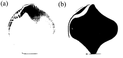
- FIG. 3A shows an X-ray topography photograph of the active layer of the compound semiconductor substrate when the lattice constants of the lower cladding layer, the active layer, and the upper cladding layer are matched so that ⁇ is 0 ′′ at room temperature. Further, an X-ray topographic photograph of the active layer of the compound semiconductor substrate when the lattice constants of the lower cladding layer, the active layer, and the upper cladding layer are matched so that ⁇ is 100 ′′ at room temperature is shown in FIG. ).
- the internal stress is relieved by setting ⁇ to 50 ′′ to 200 ′′, and dislocations are removed from the lower cladding layer / GaAs substrate removal surface.
- the second GaP layer tends to extend in the direction of the second GaP layer (see FIG. 2B)
- Dislocations such as misfit dislocations in each layer are suppressed, so that the compound semiconductor substrate of the present invention has increased emission lifetime characteristics, improved in-plane variations in emission lifetime characteristics, and further improved luminance. .
- a lower cladding layer represented by (Al x Ga 1-x ) y In 1-y P (where 0 ⁇ x ⁇ 1, 0 ⁇ y ⁇ 1), an active layer, And a light emitting layer growth step of epitaxially growing a light emitting layer comprising a double hetero structure of the upper cladding layer, A first GaP window layer growth step of epitaxially growing a first GaP window layer on the light emitting layer; Etching to remove the GaAs substrate and expose the lower cladding layer; A second GaP window layer forming step of forming a second GaP window layer on the exposed lower cladding layer, comprising: In the light emitting layer growth step, the difference ⁇ between the Bragg angle at the (400) plane of the lower cladding layer, the active layer, and the upper cladding layer and the Bragg angle at the (400) plane of the GaAs substrate is at room temperature, respectively.
- the GaAs substrate is not particularly limited as long as it is a substrate on which an AlGaInP mixed crystal is generally grown.
- a substrate having an off-angle of 2 to 15 degrees with a plane orientation (100) can be used.
- a GaAs substrate in which a compound semiconductor film such as GaAs, AlGaAs, AlGaInP, InGaP, GaP, and GaAsP is formed on the GaAs substrate can also be used.
- source gases such as TMG (trimethylgallium), TMA (trimethylaluminum), TMI (trimethylindium), AsH 3 , and PH 3 are used.
- As the semiconductor impurity gas for controlling the conductivity type DMZ (dimethyl zinc), DEZ (diethyl zinc), Cp 2 Mg, SiH 4 , H 2 Se, or the like is used.
- the compound semiconductor film thus formed can be appropriately selected depending on the use of a light emitting element such as a light emitting diode.
- a lower cladding layer represented by (Al x Ga 1-x ) y In 1-y P (where 0 ⁇ x ⁇ 1, 0 ⁇ y ⁇ 1) is formed on a GaAs substrate, A light emitting layer having a double hetero structure of an active layer and an upper cladding layer is epitaxially grown.
- the difference ⁇ between the Bragg angle at the (400) plane of the lower cladding layer, the active layer and the upper cladding layer and the Bragg angle at the (400) plane of the GaAs substrate is 50 ′′ to 50 ° C., respectively.
- the light emitting layer is epitaxially grown on the GaAs substrate so as to be 200 ′′, preferably 50 ′′ to 150 ′′, more preferably 50 ′′ to 100 ′′.
- the growth method of the light emitting layer is not particularly limited, the light emitting layer can be grown using the MOVPE method under conditions of reduced pressure of 200 mbar or less and 600 ° C. or more.
- TMG trimethyl gallium
- TMA trimethyl aluminum
- TMI trimethyl indium
- PH 3 is used also as a semiconductor impurity gas for controlling the conductivity type
- DMZ dimethyl Zinc
- DEZ diethyl zinc
- Cp 2 Mg, SiH 4 , H 2 Se and the like are used as the raw material gas.
- the adjustment conditions for each layer of the light-emitting layer made of AlGaInP are, for example, the Bragg angle of the lattice plane (400) of GaAs and (Al x Ga 1-x ) y In 1-y P (where 0 ⁇ x ⁇ 1, It is determined by measuring the Bragg angle of the lattice plane (400) of 0 ⁇ y ⁇ 1) at room temperature and comparing these to specify the adjustment conditions so that ⁇ is in the range of 50 ′′ to 200 ′′. can do.
- the first GaP window layer is epitaxially grown on the light emitting layer.
- the growth method is not particularly limited, for example, a thick transparent conductive film (GaP) can be epitaxially grown by a VPE method under conditions of 600 ° C. or higher.
- the thickness of the first GaP window layer is not particularly limited, but is preferably 10 ⁇ m to 100 ⁇ m.
- the compound semiconductor substrate having improved emission lifetime characteristics, in-plane emission lifetime characteristics variations, and brightness can be obtained by the method of manufacturing a compound semiconductor substrate of the present invention. Can be manufactured.
- the second GaP window layer can be formed by epitaxially growing the second GaP window layer on the exposed lower cladding layer or bonding a transparent conductive GaP substrate.
- the epitaxial growth method is not particularly limited, and for example, it can be performed by the VPE method under conditions of 600 ° C. or higher.
- the bonding method is not particularly limited, and the bonding can be performed by heat treatment at 100 ° C. or higher.
- the present invention provides a light emitting device manufactured from the above compound semiconductor substrate.
- a light-emitting element can be manufactured by forming Au-based P-type and N-type ohmic electrodes on the compound semiconductor substrate, and forming chips of any size, for example, 250 ⁇ m to 300 ⁇ m square ((FIG. 4 ( VI) Step). With such a light emitting element, the light emitting lifetime characteristics are increased, the variation in the light emitting lifetime characteristics among the light emitting elements is improved, and the luminance is further improved.
- Example 1 On the GaAs substrate, N-type Si doping (carrier concentration 1 ⁇ 10 18 / cm 3 ) by MOVPE method, 0.5 ⁇ m thick GaAs buffer layer and N-type Si doping (carrier concentration 1 ⁇ 10 18 / cm 3 ), An AlGaInP lower cladding layer having a thickness of 1 ⁇ m is epitaxially grown, an AlGaInP active layer having a thickness of 1 ⁇ m is epitaxially grown, and a P-type Mg-doped (carrier concentration 1 ⁇ 10 17 / cm 3 ) and an AlGaInP upper cladding layer having a thickness of 1 ⁇ m are formed. Epitaxial growth was performed (light emitting layer growth step).
- the difference ⁇ between the Bragg angle at the (400) plane of the lower cladding layer, the active layer and the upper cladding layer and the Bragg angle at the (400) plane of the GaAs substrate is 50 ′′ at room temperature.
- the crystal composition of the light emitting layer was adjusted, and the light emitting layer was epitaxially grown on the GaAs substrate.
- a P-type Mg doped (carrier concentration 3 ⁇ 10 17 / cm 3 ) and a GaP layer having a thickness of 2 ⁇ m are epitaxially grown as the first GaP window layer, and then P-type Zn doped (carrier concentration 8 ⁇ 10 17 /) by the VPE method.
- cm 3 a thick transparent conductive GaP layer having a thickness of 50 ⁇ m was epitaxially grown (first GaP window layer growth step), and then the GaAs substrate was removed by etching (etching step).
- an N-type S-doped (carrier concentration 5 ⁇ 10 17 / cm 3 ) and GaP layer having a thickness of 100 ⁇ m is epitaxially grown as a second GaP window layer by VPE (second GaP window layer forming step) to produce a compound semiconductor substrate. did.
- the Bragg angle of the lattice plane (400) of the AlGaInP active layer measured by two-crystal X-ray diffraction method the deformation lattice constant and relaxation lattice constant calculated from the Bragg angle, and the lattice mismatch between the GaAs single crystal and the AlGaInP active layer
- the rate results are also shown in Table 1.
- transformation lattice constant, a relaxation lattice constant, and a lattice mismatch rate can be calculated
- Deformation lattice constant 2 ⁇ wavelength ⁇ / sin of CuK ⁇ 1 line (Bragg angle ⁇ ′ ⁇ / 180 at the (400) plane of the AlGaInP active layer) (1)
- Relaxation lattice constant 0.47 ⁇ GaAs lattice constant + 0.53 ⁇ deformed lattice constant
- Lattice mismatch rate (relaxation lattice constant-GaAs lattice constant) / GaAs lattice constant (3)
- the GaAs lattice constant was 5.6532565.
- Example 2 A light emitting device was fabricated in the same manner as in Example 1 except that the crystal composition of the light emitting layer was adjusted so that ⁇ was 75 ′′ at room temperature, and the light emitting layer was epitaxially grown on the GaAs substrate.
- Example 3 A light emitting device was fabricated in the same manner as in Example 1 except that the crystal composition of the light emitting layer was adjusted so that ⁇ was 100 ′′ at room temperature, and the light emitting layer was epitaxially grown on the GaAs substrate.
- Example 4 A light emitting device was fabricated in the same manner as in Example 1 except that the crystal composition of the light emitting layer was adjusted so that ⁇ was 150 ′′ at room temperature, and the light emitting layer was epitaxially grown on the GaAs substrate.
- Example 5 A light emitting device was fabricated in the same manner as in Example 1 except that the crystal composition of the light emitting layer was adjusted so that ⁇ was 200 ′′ at room temperature, and the light emitting layer was epitaxially grown on the GaAs substrate.
- Example 1 A light emitting device was fabricated in the same manner as in Example 1 except that the crystal composition of the light emitting layer was adjusted so that ⁇ was ⁇ 100 ′′ at room temperature, and the light emitting layer was epitaxially grown on the GaAs substrate.
- Example 2 A light emitting device was fabricated in the same manner as in Example 1 except that the crystal composition of the light emitting layer was adjusted so that ⁇ was 0 ′′ at room temperature, and the light emitting layer was epitaxially grown on the GaAs substrate.
- Output Po (mW), emission lifetime characteristics (%) of the light emitting devices of Examples 1 to 5 and Comparative Examples 1 and 2 manufactured as described above, Bragg angle at the lattice plane (400) of the AlGaInP active layer, Table 1 shows the deformation lattice constant, relaxation lattice constant, and lattice mismatch rate.
- FIG. 5 shows the results of measuring the emission lifetime characteristics of the light-emitting elements of Examples 1 to 5 and Comparative Examples 1 and 2 and the variations in the in-plane emission lifetime characteristics.
- the horizontal axis of FIG. 5 shows the in-plane position of the compound semiconductor substrate, and the vertical axis shows the light emission lifetime characteristics corresponding to the in-plane position.
- the difference ⁇ in the vicinity of room temperature between the Bragg angle at the (400) plane of the lower cladding layer, the active layer, and the upper cladding layer and the Bragg angle at the (400) plane of the GaAs substrate is from ⁇ 100 ′′.
- a comparison with shaking up to +200 ′′ shows that the emission lifetime characteristics are increased when ⁇ is 50 ′′ to 200 ′′ (Table 1).
- in-plane variation and output (luminance) were improved at the same time as improvement of the light emission lifetime characteristics. (FIG. 5).
- Comparative Example 1 and Comparative Example 2 in which the difference ⁇ between the GaAs substrate and the AlGaInP active layer at the (400) plane is 0 ′′ to the low angle side, the internal stress balance between the layers of the compound semiconductor substrate is poor. Because dislocations (misfits, etc.) extend from the lower clad layer / GaAs substrate removal surface (second GaP layer) interface toward the light emitting layer, dislocations occur in the light emitting layer, resulting in deterioration of light emission lifetime characteristics, in-plane variation, and reduction in luminance. Was shown to occur.
- the difference ⁇ between the Bragg angle at the (400) plane of the cladding layer, the active layer, and the upper cladding layer and the Bragg angle at the (400) plane of the GaAs single crystal is 50 ′′ to 200 ′′ at room temperature, respectively.
- the present invention is not limited to the above embodiment.
- the above-described embodiment is an exemplification, and the present invention has substantially the same configuration as the technical idea described in the claims of the present invention, and any device that exhibits the same function and effect is the present invention. It is included in the technical scope of the invention.
Landscapes
- Led Devices (AREA)
Abstract
本発明は、第2GaP窓層上に、(AlxGa1-x)yIn1-yP(ただし、0<x<1、0<y<1)で示される下クラッド層、活性層、及び上クラッド層のダブルへテロ構造からなる発光層を有し、該発光層上に第1GaP窓層を有する化合物半導体基板であって、前記下クラッド層、前記活性層、及び前記上クラッド層の(400)面でのブラッグ角とGaAs単結晶の(400)面でのブラッグ角の差Δωが室温でそれぞれ50"~200"となるように、前記下クラッド層、前記活性層、及び前記上クラッド層の格子定数が整合されたものであることを特徴とする化合物半導体基板である。これにより、発光寿命特性が増大され、発光寿命特性の面内のバラツキが改善され、更に輝度が改善された高品質の化合物半導体基板を提供することを目的とする。
Description
本発明は、化合物半導体基板、及びその製造方法、並びにその化合物半導体基板を用いた発光素子に関する。
近年、例えば緑色から赤色の範囲にわたって比較的高輝度の発光が得られやすいことから、発光素子として、GaAs基板上に(AlxGa1-x)yIn1-yP(以下、単にAlGaInPと記載することがある)4元混晶からなる発光層をエピタキシャル成長させた化合物半導体基板から製造されたものがよく利用されている。
しかしながら、このようにAlGaInP等のGaAsと格子定数が異なる発光層をGaAs基板上に形成する場合、その格子定数の差が大きいほど、例えば発光素子の輝度や発光寿命特性に与える影響は大きく、それらの諸特性が低下してしまっていた。また、化合物半導体基板に転位が発生してしまうことがあった。
そこで、従来では、例えば特許文献1に開示されているように、AlGaInPをエピタキシャル成長させる時において、AlGaInPとGaAsの格子面(400)のブラッグ角の差Δωが0″~低角となるように、AlGaInPとGaAsとの格子定数を整合させて、AlGaInPの組成を調整し、発光層を形成する方法が行われていた。
また、GaAsからAlGaInPの格子定数まで徐々に混晶率が変化する層を形成したり、不整合を緩和する層を形成したりすることにより、エピタキシャル成長させたAlGaInP層の格子定数をGaAsの格子定数に近づける試みが行われていた。
しかしながら、このような従来のエピタキシャル成長温度における格子定数を考慮した製造方法や、AlGaInPとGaAsとの格子定数の差を小さくするための層を間に形成する製造方法のみでは、製造された発光素子(化合物半導体基板)の輝度および発光寿命特性等の諸特性が不安定であり、必ずしも満足する結果が得られていなかった。
さらに、AlGaInPをエピタキシャル成長させる時において、AlGaInPとGaAsの格子面(400)のブラッグ角の差Δωが0″~低角となるように、AlGaInPとGaAsとの格子定数を整合させて、AlGaInPの組成を調整し、発光層を形成する方法の場合には、発光層へ転位が伝播しやすいため、化合物半導体基板全体の発光寿命特性の劣化や、化合物半導体基板面内における発光寿命特性のバラツキが生じ、またその劣化やバラツキの程度もバッチ間で不安定となることが分かった。
本発明は、上記課題を解決するためになされたもので、発光層への転位の伝播が抑制されることで、発光寿命特性が増大され、発光寿命特性の面内のバラツキが改善され、更に輝度が改善された高品質の化合物半導体基板、及びその製造方法を提供することを目的とする。更に、本発明では、前記化合物半導体基板を用いた発光素子を提供することを目的とする。
本発明では、第2GaP窓層上に、(AlxGa1-x)yIn1-yP(ただし、0<x<1、0<y<1)で示される下クラッド層、活性層、及び上クラッド層のダブルへテロ構造からなる発光層を有し、該発光層上に第1GaP窓層を有する化合物半導体基板であって、
前記下クラッド層、前記活性層、及び前記上クラッド層の(400)面でのブラッグ角とGaAs単結晶の(400)面でのブラッグ角の差Δω(以下、単にΔωと記載することがある)が室温でそれぞれ50″~200″となるように、前記下クラッド層、前記活性層、及び前記上クラッド層の格子定数が整合されたものであることを特徴とする化合物半導体基板を提供する。
前記下クラッド層、前記活性層、及び前記上クラッド層の(400)面でのブラッグ角とGaAs単結晶の(400)面でのブラッグ角の差Δω(以下、単にΔωと記載することがある)が室温でそれぞれ50″~200″となるように、前記下クラッド層、前記活性層、及び前記上クラッド層の格子定数が整合されたものであることを特徴とする化合物半導体基板を提供する。
このように、Δωが室温でそれぞれ50″~200″となるように、下クラッド層、活性層、及び上クラッド層の格子定数を整合された化合物半導体基板であれば、化合物半導体基板の各層間の応力緩和が有効に働き、ミスフィット転位等の転位の発光層各層への伝播が抑制されたものとなるため、発光寿命特性が増大され、発光寿命特性の面内のバラツキが改善され、更に輝度が改善された化合物半導体基板となる。
また、Δωが室温でそれぞれ50″~150″、特には50″~100″となるように、下クラッド層、活性層、及び上クラッド層の格子定数が整合されたものであることが好ましい。
このようなΔωの範囲であれば、化合物半導体基板の各層間の応力緩和がより有効に働き、ミスフィット転位等の転位の発光層各層への伝播が抑制されたものとなるため、一層、発光寿命特性が増大され、発光寿命特性の面内のバラツキが改善され、更に輝度が改善された化合物半導体基板となる。
さらに、本発明では、前記化合物半導体基板から製造されたものであることを特徴とする発光素子を提供する。
このような発光素子であれば、発光寿命特性が増大され、発光素子間で発光寿命特性のバラツキが改善され、更に輝度が改善された発光素子となる。
また、本発明では、GaAs基板上に、(AlxGa1-x)yIn1-yP(ただし、0<x<1、0<y<1)で示される下クラッド層、活性層、及び上クラッド層のダブルへテロ構造からなる発光層をエピタキシャル成長する発光層成長工程と、
前記発光層上に第1GaP窓層をエピタキシャル成長する第1GaP窓層成長工程と、
前記GaAs基板をエッチング除去し、前記下クラッド層を露出させるエッチング工程と、
前記露出した下クラッド層上に第2GaP窓層を形成する第2GaP窓層形成工程とを含む化合物半導体基板の製造方法であって、
前記発光層成長工程において、前記下クラッド層、前記活性層、及び前記上クラッド層の(400)面でのブラッグ角と前記GaAs基板の(400)面でのブラッグ角の差Δωが室温でそれぞれ50″~200″となるように、前記GaAs基板上に前記発光層をエピタキシャル成長することを特徴とする化合物半導体基板の製造方法を提供する。
前記発光層上に第1GaP窓層をエピタキシャル成長する第1GaP窓層成長工程と、
前記GaAs基板をエッチング除去し、前記下クラッド層を露出させるエッチング工程と、
前記露出した下クラッド層上に第2GaP窓層を形成する第2GaP窓層形成工程とを含む化合物半導体基板の製造方法であって、
前記発光層成長工程において、前記下クラッド層、前記活性層、及び前記上クラッド層の(400)面でのブラッグ角と前記GaAs基板の(400)面でのブラッグ角の差Δωが室温でそれぞれ50″~200″となるように、前記GaAs基板上に前記発光層をエピタキシャル成長することを特徴とする化合物半導体基板の製造方法を提供する。
このような発光層成長工程を有する化合物半導体基板の製造方法であれば、製造時において、化合物半導体基板の各層間の応力緩和が有効に働き、ミスフィット転位等の転位が発光層各層に伝播しにくいため、発光寿命特性が増大され、発光寿命特性の面内のバラツキが改善され、更に輝度が改善された化合物半導体基板を製造することができる方法となる。
また、発光層成長工程において、前記Δωが室温でそれぞれ50″~150″、特には50″~100″となるように、GaAs基板上に発光層をエピタキシャル成長することが好ましい。
このような発光層成長工程であれば、製造時において、化合物半導体基板の各層間の応力緩和がより有効に働き、ミスフィット転位等の転位が発光層各層により伝播しにくくなるため、一層、発光寿命特性が増大され、発光寿命特性の面内のバラツキが改善され、更に輝度が改善された化合物半導体基板を製造することができる方法となる。
以上説明したように、下クラッド層、活性層、及び上クラッド層の(400)面でのブラッグ角とGaAs単結晶の(400)面でのブラッグ角の差Δωが室温でそれぞれ50″~200″となるように、下クラッド層、活性層、及び上クラッド層の格子定数を整合する本発明の化合物半導体基板であれば、化合物半導体基板の各層間の応力が緩和され、ミスフィット転位等の転位の発光層各層への伝播が抑制されたものとなるので、発光寿命特性が増大され、発光寿命特性の面内のバラツキが改善され、更に輝度が改善された化合物半導体基板となる。
以下、本発明をより詳細に説明するが、本発明はこれに限定されるものではない。前述のように、発光層への転位の伝播が抑制された化合物半導体基板が望まれていた。
本発明者らは、上記課題に対し鋭意検討を重ねた結果、下クラッド層、活性層、及び上クラッド層の(400)面でのブラッグ角とGaAs単結晶の(400)面でのブラッグ角の差Δωが室温でそれぞれ50″~200″となるように、下クラッド層、活性層、及び上クラッド層の格子定数を整合された化合物半導体基板であれば、化合物半導体基板の各層間の応力が緩和されることを見出し、これにより発光層へのミスフィット転位等の転位の伝播が抑制され、発光寿命特性、面内の発光寿命特性のバラツキ、及び輝度が改善されることを見出して、本発明を完成させた。以下、図1~5を参照して、詳細に説明する。
[化合物半導体基板]
本発明では、第2GaP窓層上に、(AlxGa1-x)yIn1-yP(ただし、0<x<1、0<y<1)で示される下クラッド層、活性層、及び上クラッド層のダブルへテロ構造からなる発光層を有し、該発光層上に第1GaP窓層を有する化合物半導体基板であって、
前記下クラッド層、前記活性層、及び前記上クラッド層の(400)面でのブラッグ角とGaAs単結晶の(400)面でのブラッグ角の差Δωが室温でそれぞれ50″~200″となるように、前記下クラッド層、前記活性層、及び前記上クラッド層の格子定数が整合されたものであることを特徴とする化合物半導体基板を提供する。
本発明では、第2GaP窓層上に、(AlxGa1-x)yIn1-yP(ただし、0<x<1、0<y<1)で示される下クラッド層、活性層、及び上クラッド層のダブルへテロ構造からなる発光層を有し、該発光層上に第1GaP窓層を有する化合物半導体基板であって、
前記下クラッド層、前記活性層、及び前記上クラッド層の(400)面でのブラッグ角とGaAs単結晶の(400)面でのブラッグ角の差Δωが室温でそれぞれ50″~200″となるように、前記下クラッド層、前記活性層、及び前記上クラッド層の格子定数が整合されたものであることを特徴とする化合物半導体基板を提供する。
〔第1GaP窓層及び第2GaP窓層〕
本発明における第1GaP窓層1及び第2GaP窓層6は、GaPからなる透明導電性膜であれば特に限定されない(図1)。第1GaP窓層及び第2GaP窓層は、例えば厚膜透明導電性膜とすることができ、第1GaP窓層の厚さとしては、10μm~100μmが好ましい。また、第2GaP窓層の厚さとしては、10μm~100μmが好ましい。このように厚膜の第1GaP窓層及び第2GaP窓層であっても、本発明の化合物半導体基板であれば発光寿命特性、面内の発光寿命特性のバラツキ、及び輝度が改善されたものとなる。
本発明における第1GaP窓層1及び第2GaP窓層6は、GaPからなる透明導電性膜であれば特に限定されない(図1)。第1GaP窓層及び第2GaP窓層は、例えば厚膜透明導電性膜とすることができ、第1GaP窓層の厚さとしては、10μm~100μmが好ましい。また、第2GaP窓層の厚さとしては、10μm~100μmが好ましい。このように厚膜の第1GaP窓層及び第2GaP窓層であっても、本発明の化合物半導体基板であれば発光寿命特性、面内の発光寿命特性のバラツキ、及び輝度が改善されたものとなる。
また、第1GaP窓層及び第2GaP窓層は電流拡散層であることが好ましい。第1GaP窓層及び第2GaP窓層が電流拡散層であれば、電極の近傍だけでなく、広い範囲で効率よく発光させることが可能となる。
〔発光層〕
本発明における発光層5は、(AlxGa1-x)yIn1-yP(ただし、0<x<1、0<y<1)で示される下クラッド層4、活性層3、及び上クラッド層2のダブルへテロ構造からなる(図1)。
本発明における発光層5は、(AlxGa1-x)yIn1-yP(ただし、0<x<1、0<y<1)で示される下クラッド層4、活性層3、及び上クラッド層2のダブルへテロ構造からなる(図1)。
下クラッド層4、活性層3、及び上クラッド層2の格子定数は、下クラッド層4、活性層3、及び上クラッド層2の(400)面でのブラッグ角とGaAs単結晶の(400)面でのブラッグ角の差Δωが室温でそれぞれ50″~200″、好ましくは50″~150″、より好ましくは50″~100″となるように、整合されたものである。
Δωの算出としては、測定用のX線として波長λ=1.5405ÅのCuKα1線を用い、GaAs基板の(400)面でのブラッグ角ωとAlGaInP下クラッド層、活性層、上クラッド層の(400)面でのブラッグ角ω’をそれぞれ測定し、その差Δω(=ω’-ω)を求めることで行うことができる。
このように、Δωが室温でそれぞれ50″~200″、好ましくは50″~150″、より好ましくは50″~100″となるように、下クラッド層、活性層、及び上クラッド層の格子定数を整合されることにより、化合物半導体基板の各層間の応力緩和が有効に働き、ミスフィット転位等の転位の発光層各層への伝播が抑制されたものとなる。そのため、発光寿命特性が増大され、発光寿命特性の面内のバラツキが改善され、更に輝度が改善された化合物半導体基板となる。以下、図2、3を参照してより詳細に説明する。
Δωが室温でそれぞれ0″~低角となるように、下クラッド層、活性層、及び上クラッド層の格子定数を整合した場合の化合物半導体基板の概略断面図図2(a)に、内部応力に伴う転位の伝播方向を示した。また、Δωが室温でそれぞれ50″~200″となるように、下クラッド層、活性層、及び上クラッド層の格子定数を整合した場合の化合物半導体基板の概略断面図図2(b)に、内部応力に伴う転位の伝播方向を示した。
図2(a)に示すようにΔωが室温でそれぞれ0″~低角であると、(AlxGa1-x)yIn1-yP(ただし、0<x<1、0<y<1)で示される下クラッド層、活性層、及び上クラッド層に圧縮圧力がかかり、下クラッド層、活性層、及び上クラッド層にミスフィット転位等の転位が伝播する。これにより、従来は化合物半導体基板の発光寿命特性が劣化し、化合物半導体基板面内の発光寿命特性のバラツキが生じ、更に輝度が悪化していた。一方で、図2(b)に示すようにΔωが室温でそれぞれ50″~200″であると、下クラッド層、活性層、及び上クラッド層にかかる応力は緩和され、下クラッド層、活性層、及び上クラッド層のミスフィット転位などの転位の伝播は抑制される。これにより、本発明の化合物半導体基板では発光寿命特性が増大され、発光寿命特性の面内のバラツキが改善され、更に輝度が改善されたものとなる。
Δωと転位の関係を示すために、化合物半導体基板の下クラッド層と第2GaP窓層の界面のX線トポグラフィ写真を撮影した。Δωが室温でそれぞれ0″となるように、下クラッド層、活性層、及び上クラッド層の格子定数を整合した場合の化合物半導体基板の活性層のX線トポグラフィ写真を図3(a)に示す。また、Δωが室温でそれぞれ100″となるように、下クラッド層、活性層、及び上クラッド層の格子定数を整合した場合の化合物半導体基板の活性層のX線トポグラフィ写真を図3(b)に示す。
Δωが室温でそれぞれ0″であると下クラッド層、活性層、及び上クラッド層に圧縮圧力がかかり、化合物半導体基板の各層間の内部応力バランスが悪くなる。これにより、転位(ミスフィット等)が下クラッド層/GaAs基板除去面(第2GaP層)界面から発光層方向に伸びる(図2(a)参照)。その結果、図3(a)に示すように活性層など発光層各層に転位が生じ、発光寿命特性の悪化、面内のバラツキ、輝度の低下が生じることとなる。
一方で、本発明の化合物半導体基板のようにΔωが室温でそれぞれ100″であると、Δωを50″~200″にする事で内部応力が緩和され、転位が下クラッド層/GaAs基板除去面(第2GaP層)界面から発光層方向へ伸びるのに代わり、第2GaP層方向に伸びやすい(図2(b)参照)。その結果、図3(b)に示すように、活性層など発光層各層のミスフィット転位などの転位は抑制される。そのため、本発明の化合物半導体基板は発光寿命特性が増大され、発光寿命特性の面内のバラツキが改善され、更に輝度が改善されたものとなる。
[化合物半導体基板の製造方法]
また、本発明では、GaAs基板上に、(AlxGa1-x)yIn1-yP(ただし、0<x<1、0<y<1)で示される下クラッド層、活性層、及び上クラッド層のダブルへテロ構造からなる発光層をエピタキシャル成長する発光層成長工程と、
前記発光層上に第1GaP窓層をエピタキシャル成長する第1GaP窓層成長工程と、
前記GaAs基板をエッチング除去し、前記下クラッド層を露出させるエッチング工程と、
前記露出した下クラッド層上に第2GaP窓層を形成する第2GaP窓層形成工程とを含む化合物半導体基板の製造方法であって、
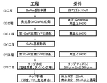
前記発光層成長工程において、前記下クラッド層、前記活性層、及び前記上クラッド層の(400)面でのブラッグ角と前記GaAs基板の(400)面でのブラッグ角の差Δωが室温でそれぞれ50″~200″となるように、前記GaAs基板上に前記発光層をエピタキシャル成長することを特徴とする化合物半導体基板の製造方法を提供する。以下、図4を参照して詳細に説明する。
また、本発明では、GaAs基板上に、(AlxGa1-x)yIn1-yP(ただし、0<x<1、0<y<1)で示される下クラッド層、活性層、及び上クラッド層のダブルへテロ構造からなる発光層をエピタキシャル成長する発光層成長工程と、
前記発光層上に第1GaP窓層をエピタキシャル成長する第1GaP窓層成長工程と、
前記GaAs基板をエッチング除去し、前記下クラッド層を露出させるエッチング工程と、
前記露出した下クラッド層上に第2GaP窓層を形成する第2GaP窓層形成工程とを含む化合物半導体基板の製造方法であって、
前記発光層成長工程において、前記下クラッド層、前記活性層、及び前記上クラッド層の(400)面でのブラッグ角と前記GaAs基板の(400)面でのブラッグ角の差Δωが室温でそれぞれ50″~200″となるように、前記GaAs基板上に前記発光層をエピタキシャル成長することを特徴とする化合物半導体基板の製造方法を提供する。以下、図4を参照して詳細に説明する。
〔GaAs基板の準備(図4の(I)工程)〕
GaAs基板としては、一般にAlGaInP混晶を成長させる基板となるものであれば特に制限されないが、例えば面方位(100)のオフアングル2~15度のものを用いることができる。このGaAs基板上に、GaAs、AlGaAs、AlGaInP、InGaP、GaP、GaAsPなどの化合物半導体膜が形成されたGaAs基板も用いることができる。これらの化合物半導体膜をMOVPE法でGaAs基板上に形成する場合は、TMG(トリメチルガリウム)、TMA(トリメチルアルミニウム)、TMI(トリメチルインジウム)、AsH3、PH3などの原料ガスが用いられ、また、導電型を制御するための半導体不純物用ガスとしては、DMZ(ジメチルジンク)、DEZ(ジエチルジンク)やCp2Mg、SiH4、H2Seなどが用いられる。このようにして形成される化合物半導体膜は、例えば発光ダイオードなどの発光素子等の用途に応じて適宜選択することができる。
GaAs基板としては、一般にAlGaInP混晶を成長させる基板となるものであれば特に制限されないが、例えば面方位(100)のオフアングル2~15度のものを用いることができる。このGaAs基板上に、GaAs、AlGaAs、AlGaInP、InGaP、GaP、GaAsPなどの化合物半導体膜が形成されたGaAs基板も用いることができる。これらの化合物半導体膜をMOVPE法でGaAs基板上に形成する場合は、TMG(トリメチルガリウム)、TMA(トリメチルアルミニウム)、TMI(トリメチルインジウム)、AsH3、PH3などの原料ガスが用いられ、また、導電型を制御するための半導体不純物用ガスとしては、DMZ(ジメチルジンク)、DEZ(ジエチルジンク)やCp2Mg、SiH4、H2Seなどが用いられる。このようにして形成される化合物半導体膜は、例えば発光ダイオードなどの発光素子等の用途に応じて適宜選択することができる。
〔発光層成長工程(図4の(II)工程)〕
本発明における発光層成長工程では、GaAs基板上に、(AlxGa1-x)yIn1-yP(ただし、0<x<1、0<y<1)で示される下クラッド層、活性層、及び上クラッド層のダブルへテロ構造からなる発光層をエピタキシャル成長する。この発光層成長工程では、下クラッド層、活性層、及び上クラッド層の(400)面でのブラッグ角と前記GaAs基板の(400)面でのブラッグ角の差Δωが室温でそれぞれ50″~200″、好ましくは50″~150″、より好ましくは50″~100″となるように、GaAs基板上に発光層をエピタキシャル成長する。発光層の成長方法としては特に制限されないが、減圧200mbar以下、600℃以上の条件でMOVPE法を用いて行うことができる。例えば、原料ガスとしてはTMG(トリメチルガリウム)、TMA(トリメチルアルミニウム)、TMI(トリメチルインジウム)、PH3などが用いられ、また、導電型を制御するための半導体不純物用ガスとしては、DMZ(ジメチルジンク)、DEZ(ジエチルジンク)やCp2Mg、SiH4、H2Seなどが用いられる。
本発明における発光層成長工程では、GaAs基板上に、(AlxGa1-x)yIn1-yP(ただし、0<x<1、0<y<1)で示される下クラッド層、活性層、及び上クラッド層のダブルへテロ構造からなる発光層をエピタキシャル成長する。この発光層成長工程では、下クラッド層、活性層、及び上クラッド層の(400)面でのブラッグ角と前記GaAs基板の(400)面でのブラッグ角の差Δωが室温でそれぞれ50″~200″、好ましくは50″~150″、より好ましくは50″~100″となるように、GaAs基板上に発光層をエピタキシャル成長する。発光層の成長方法としては特に制限されないが、減圧200mbar以下、600℃以上の条件でMOVPE法を用いて行うことができる。例えば、原料ガスとしてはTMG(トリメチルガリウム)、TMA(トリメチルアルミニウム)、TMI(トリメチルインジウム)、PH3などが用いられ、また、導電型を制御するための半導体不純物用ガスとしては、DMZ(ジメチルジンク)、DEZ(ジエチルジンク)やCp2Mg、SiH4、H2Seなどが用いられる。
AlGaInPからなる発光層各層の調整条件は、例えば、GaAsの格子面(400)の室温でのブラッグ角と(AlxGa1-x)yIn1-yP(ただし、0<x<1、0<y<1)の格子面(400)の室温におけるブラッグ角を測定しておき、これらを比較してΔωが50″~200″の範囲になるような調整条件を予め特定することで決定することができる。
〔第1GaP窓層成長工程(図4の(III)工程)〕
本発明における第1GaP窓層成長工程では、発光層上に第1GaP窓層をエピタキシャル成長する。成長方法は特に限定されないが、例えば600℃以上の条件でVPE法により厚膜透明導電性膜(GaP)をエピタキシャル成長させることができる。第1GaP窓層の厚さとしては、特に制限されないが10μm~100μmが好ましい。このように厚膜の第1GaP窓層であっても、本発明の化合物半導体基板の製造方法であれば発光寿命特性、面内の発光寿命特性のバラツキ、及び輝度が改善された化合物半導体基板を製造することができる。
本発明における第1GaP窓層成長工程では、発光層上に第1GaP窓層をエピタキシャル成長する。成長方法は特に限定されないが、例えば600℃以上の条件でVPE法により厚膜透明導電性膜(GaP)をエピタキシャル成長させることができる。第1GaP窓層の厚さとしては、特に制限されないが10μm~100μmが好ましい。このように厚膜の第1GaP窓層であっても、本発明の化合物半導体基板の製造方法であれば発光寿命特性、面内の発光寿命特性のバラツキ、及び輝度が改善された化合物半導体基板を製造することができる。
〔エッチング工程(図4の(VI)工程)〕
本発明におけるエッチング工程では、GaAs基板をエッチング除去し、下クラッド層を露出させる。
本発明におけるエッチング工程では、GaAs基板をエッチング除去し、下クラッド層を露出させる。
〔第2GaP窓層形成工程(図4の(V)工程)〕
本発明における第2GaP窓層形成工程では、露出した下クラッド層上に第2GaP窓層をエピタキシャル成長し、又は透明導電性GaP基板を接合することで第2GaP窓層を形成することができる。エピタキシャル成長方法は特に限定されず、例えば600℃以上の条件でVPE法により行うことができる。また、接合方法も特に制限されず、100℃以上で熱処理することで接合することができる。
本発明における第2GaP窓層形成工程では、露出した下クラッド層上に第2GaP窓層をエピタキシャル成長し、又は透明導電性GaP基板を接合することで第2GaP窓層を形成することができる。エピタキシャル成長方法は特に限定されず、例えば600℃以上の条件でVPE法により行うことができる。また、接合方法も特に制限されず、100℃以上で熱処理することで接合することができる。
[発光素子]
さらに、本発明では上記化合物半導体基板から製造されたものであることを特徴とする発光素子を提供する。特に制限されないが、上記化合物半導体基板にAu系P型及びN型のオーミック電極を形成し、任意のサイズ、例えば250μm~300μm角にチップ化して発光素子を製造することができる(図4の(VI)工程)。このような発光素子であれば、発光寿命特性が増大され、発光素子間で発光寿命特性のバラツキが改善され、更に輝度が改善された発光素子となる。
さらに、本発明では上記化合物半導体基板から製造されたものであることを特徴とする発光素子を提供する。特に制限されないが、上記化合物半導体基板にAu系P型及びN型のオーミック電極を形成し、任意のサイズ、例えば250μm~300μm角にチップ化して発光素子を製造することができる(図4の(VI)工程)。このような発光素子であれば、発光寿命特性が増大され、発光素子間で発光寿命特性のバラツキが改善され、更に輝度が改善された発光素子となる。
以下、本発明の実施例および比較例をあげてさらに詳細に説明するが、本発明は下記の実施例に限定されるものではない。
(実施例1)
GaAs基板上に、MOVPE法によってN型Siドープ(キャリア濃度1×10¹⁸/cm3)、厚さ0.5μmのGaAsバッファー層とN型Siドープ(キャリア濃度1×1018/cm3)、厚さ1μmのAlGaInP下クラッド層をエピタキシャル成長させ、ノンドープ、厚さ1μmのAlGaInP活性層をエピタキシャル成長させ、P型Mgドープ(キャリア濃度1×1017/cm3)、厚さ1μmのAlGaInP上クラッド層をエピタキシャル成長させた(発光層成長工程)。
GaAs基板上に、MOVPE法によってN型Siドープ(キャリア濃度1×10¹⁸/cm3)、厚さ0.5μmのGaAsバッファー層とN型Siドープ(キャリア濃度1×1018/cm3)、厚さ1μmのAlGaInP下クラッド層をエピタキシャル成長させ、ノンドープ、厚さ1μmのAlGaInP活性層をエピタキシャル成長させ、P型Mgドープ(キャリア濃度1×1017/cm3)、厚さ1μmのAlGaInP上クラッド層をエピタキシャル成長させた(発光層成長工程)。
この発光層成長工程において、下クラッド層、活性層、及び上クラッド層の(400)面でのブラッグ角と前記GaAs基板の(400)面でのブラッグ角の差Δωが室温でそれぞれ50″となるように、発光層の結晶組成を調整して、GaAs基板上に発光層をエピタキシャル成長させた。
続いて、第1GaP窓層としてP型Mgドープ(キャリア濃度3×10¹⁷/cm3)、厚さ2μmのGaP層をエピタキシャル成長させ、その後VPE法でP型Znドープ(キャリア濃度8×1017/cm3)、厚さ50μmの厚膜透明導電性GaP層をエピタキシャル成長させ(第1GaP窓層成長工程)、その後にGaAs基板をエッチング除去した(エッチング工程)。最後に、VPE法で第2GaP窓層としてN型Sドープ(キャリア濃度5×1017/cm3)、厚さ100μmのGaP層をエピタキシャル成長させて(第2GaP窓層形成工程)化合物半導体基板を作製した。
この化合物半導体基板にAu系P型及びN型のオーミック電極を形成し、任意のサイズにチップ化して発光素子を製造した。このようにして製造された本発明の発光素子の輝度および発光寿命特性を測定した。測定時の温度は85℃、湿度は45%とし、電流20mAでの発光出力Po(mW)を測定し、また、50mA以上の電流を100時間通電させた後に再度発光出力を測定し、発光寿命特性(%)を算出した。その測定結果を表1に示す。
また、2結晶X線回折法により測定したAlGaInP活性層の格子面(400)のブラッグ角、該ブラッグ角から算出した変形格子定数並びに緩和格子定数、及びGaAs単結晶とAlGaInP活性層の格子不整合率の結果も表1に示す。なお、2結晶X線回折法では測定用のX線として波長λ=1.5405ÅのCuKα1線を用いた。
なお、変形格子定数、緩和格子定数、及び格子不整合率は下記式(1)、(2)、(3)で求めることができる。
変形格子定数=2×CuKα1線の波長λ/sin(AlGaInP活性層の(400)面でのブラッグ角ω’π/180) ……(1)
緩和格子定数=0.47×GaAs格子定数+0.53×変形格子定数 ……(2)
格子不整合率=(緩和格子定数-GaAs格子定数)/GaAs格子定数……(3)
ここで、GaAs格子定数は5.65325Åとした。
変形格子定数=2×CuKα1線の波長λ/sin(AlGaInP活性層の(400)面でのブラッグ角ω’π/180) ……(1)
緩和格子定数=0.47×GaAs格子定数+0.53×変形格子定数 ……(2)
格子不整合率=(緩和格子定数-GaAs格子定数)/GaAs格子定数……(3)
ここで、GaAs格子定数は5.65325Åとした。
(実施例2)
Δωが室温でそれぞれ75″となるように、発光層の結晶組成を調整して、GaAs基板上に発光層をエピタキシャル成長させた以外は実施例1と同様にして発光素子を作製した。
Δωが室温でそれぞれ75″となるように、発光層の結晶組成を調整して、GaAs基板上に発光層をエピタキシャル成長させた以外は実施例1と同様にして発光素子を作製した。
(実施例3)
Δωが室温でそれぞれ100″となるように、発光層の結晶組成を調整して、GaAs基板上に発光層をエピタキシャル成長させた以外は実施例1と同様にして発光素子を作製した。
Δωが室温でそれぞれ100″となるように、発光層の結晶組成を調整して、GaAs基板上に発光層をエピタキシャル成長させた以外は実施例1と同様にして発光素子を作製した。
(実施例4)
Δωが室温でそれぞれ150″となるように、発光層の結晶組成を調整して、GaAs基板上に発光層をエピタキシャル成長させた以外は実施例1と同様にして発光素子を作製した。
Δωが室温でそれぞれ150″となるように、発光層の結晶組成を調整して、GaAs基板上に発光層をエピタキシャル成長させた以外は実施例1と同様にして発光素子を作製した。
(実施例5)
Δωが室温でそれぞれ200″となるように、発光層の結晶組成を調整して、GaAs基板上に発光層をエピタキシャル成長させた以外は実施例1と同様にして発光素子を作製した。
Δωが室温でそれぞれ200″となるように、発光層の結晶組成を調整して、GaAs基板上に発光層をエピタキシャル成長させた以外は実施例1と同様にして発光素子を作製した。
(比較例1)
Δωが室温でそれぞれ-100″となるように、発光層の結晶組成を調整して、GaAs基板上に発光層をエピタキシャル成長させた以外は実施例1と同様にして発光素子を作製した。
Δωが室温でそれぞれ-100″となるように、発光層の結晶組成を調整して、GaAs基板上に発光層をエピタキシャル成長させた以外は実施例1と同様にして発光素子を作製した。
(比較例2)
Δωが室温でそれぞれ0″となるように、発光層の結晶組成を調整して、GaAs基板上に発光層をエピタキシャル成長させた以外は実施例1と同様にして発光素子を作製した。
Δωが室温でそれぞれ0″となるように、発光層の結晶組成を調整して、GaAs基板上に発光層をエピタキシャル成長させた以外は実施例1と同様にして発光素子を作製した。
以上のようにして製造された実施例1~5、比較例1~2の発光素子の出力Po(mW)、発光寿命特性(%)、AlGaInP活性層の格子面(400)でのブラッグ角、変形格子定数、緩和格子定数、格子不整合率を表1に示す。
さらに、実施例1~5、比較例1~2の発光素子の発光寿命特性と、面内での発光寿命特性のバラツキを測定した結果を図5に示す。図5の横軸は化合物半導体基板の面内位置を示し、縦軸はその面内位置に対応する発光寿命特性を示す。
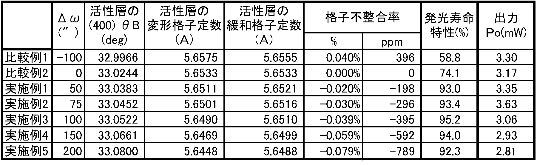
以上のように、下クラッド層、活性層、及び上クラッド層の(400)面でのブラッグ角と前記GaAs基板の(400)面でのブラッグ角の室温付近での差Δωを-100″から+200″まで振って比較すると、Δωが50″~200″のときに発光寿命特性が上昇していることがわかる(表1)。さらに、Δωが50″~200″である本発明の化合物半導体基板の実施例1~5では発光寿命特性の向上と同時に面内のバラツキ、出力(輝度)も改善されていることが示された(図5)。
一方で、GaAs基板とAlGaInP活性層の(400)面でのブラッグ角の差Δωが0″から低角側の比較例1及び比較例2では、化合物半導体基板の各層間の内部応力バランスが悪く、転位(ミスフィット等)が下クラッド層/GaAs基板除去面(第2GaP層)界面から発光層方向に伸びるため、発光層に転位が生じ発光寿命特性の悪化、面内のバラツキ、輝度の低下が生じていることが示された。
以上説明したように、クラッド層、活性層、及び上クラッド層の(400)面でのブラッグ角とGaAs単結晶の(400)面でのブラッグ角の差Δωが室温でそれぞれ50″~200″となるように、下クラッド層、活性層、及び上クラッド層の格子定数を整合する本発明の化合物半導体基板であれば、化合物半導体基板の各層間の応力が緩和され、ミスフィット転位等の転位の発光層各層への伝播が抑制されたものとなるので、発光寿命特性が増大され、発光寿命特性の面内のバラツキが改善され、更に輝度が改善された化合物半導体基板となる。
なお、本発明は、上記実施形態に限定されるものではない。上記実施形態は、例示であり、本発明の特許請求の範囲に記載された技術的思想と実質的に同一な構成を有し、同様な作用効果を奏するものは、いかなるものであっても本発明の技術的範囲に包含される。
Claims (7)
- 第2GaP窓層上に、(AlxGa1-x)yIn1-yP(ただし、0<x<1、0<y<1)で示される下クラッド層、活性層、及び上クラッド層のダブルへテロ構造からなる発光層を有し、該発光層上に第1GaP窓層を有する化合物半導体基板であって、
前記下クラッド層、前記活性層、及び前記上クラッド層の(400)面でのブラッグ角とGaAs単結晶の(400)面でのブラッグ角の差Δωが室温でそれぞれ50″~200″となるように、前記下クラッド層、前記活性層、及び前記上クラッド層の格子定数が整合されたものであることを特徴とする化合物半導体基板。
- 前記Δωが室温でそれぞれ50″~150″となるように、前記下クラッド層、前記活性層、及び前記上クラッド層の格子定数が整合されたものであることを特徴とする請求項1に記載の化合物半導体基板。
- 前記Δωが室温でそれぞれ50″~100″となるように、前記下クラッド層、前記活性層、及び前記上クラッド層の格子定数が整合されたものであることを特徴とする請求項1又は請求項2に記載の化合物半導体基板。
- 請求項1乃至請求項3のいずれか一項に記載の化合物半導体基板から製造されたものであることを特徴とする発光素子。
- GaAs基板上に、(AlxGa1-x)yIn1-yP(ただし、0<x<1、0<y<1)で示される下クラッド層、活性層、及び上クラッド層のダブルへテロ構造からなる発光層をエピタキシャル成長する発光層成長工程と、
前記発光層上に第1GaP窓層をエピタキシャル成長する第1GaP窓層成長工程と、
前記GaAs基板をエッチング除去し、前記下クラッド層を露出させるエッチング工程と、
前記露出した下クラッド層上に第2GaP窓層を形成する第2GaP窓層形成工程とを含む化合物半導体基板の製造方法であって、
前記発光層成長工程において、前記下クラッド層、前記活性層、及び前記上クラッド層の(400)面でのブラッグ角と前記GaAs基板の(400)面でのブラッグ角の差Δωが室温でそれぞれ50″~200″となるように、前記GaAs基板上に前記発光層をエピタキシャル成長することを特徴とする化合物半導体基板の製造方法。
- 前記発光層成長工程において、前記Δωが室温でそれぞれ50″~150″となるように、前記GaAs基板上に前記発光層をエピタキシャル成長することを特徴とする請求項5に記載の化合物半導体基板の製造方法。
- 前記発光層成長工程において、前記Δωが室温でそれぞれ50″~100″となるように、前記GaAs基板上に前記発光層をエピタキシャル成長することを特徴とする請求項5又は請求項6に記載の化合物半導体基板の製造方法。
Priority Applications (1)
| Application Number | Priority Date | Filing Date | Title |
|---|---|---|---|
| JP2013517844A JP5768879B2 (ja) | 2011-06-02 | 2012-05-16 | 化合物半導体基板、及びその製造方法、並びにその化合物半導体基板を用いた発光素子 |
Applications Claiming Priority (2)
| Application Number | Priority Date | Filing Date | Title |
|---|---|---|---|
| JP2011124564 | 2011-06-02 | ||
| JP2011-124564 | 2011-06-02 |
Publications (1)
| Publication Number | Publication Date |
|---|---|
| WO2012164847A1 true WO2012164847A1 (ja) | 2012-12-06 |
Family
ID=47258724
Family Applications (1)
| Application Number | Title | Priority Date | Filing Date |
|---|---|---|---|
| PCT/JP2012/003192 Ceased WO2012164847A1 (ja) | 2011-06-02 | 2012-05-16 | 化合物半導体基板、及びその製造方法、並びにその化合物半導体基板を用いた発光素子 |
Country Status (3)
| Country | Link |
|---|---|
| JP (1) | JP5768879B2 (ja) |
| TW (1) | TW201316378A (ja) |
| WO (1) | WO2012164847A1 (ja) |
Citations (5)
| Publication number | Priority date | Publication date | Assignee | Title |
|---|---|---|---|---|
| JPH09186360A (ja) * | 1995-12-28 | 1997-07-15 | Showa Denko Kk | AlGaInP発光ダイオード |
| JP2005093895A (ja) * | 2003-09-19 | 2005-04-07 | Sumitomo Electric Ind Ltd | ZnSe系発光素子 |
| JP2010141201A (ja) * | 2008-12-12 | 2010-06-24 | Shin Etsu Handotai Co Ltd | 化合物半導体基板および発光素子ならびに化合物半導体基板の製造方法および発光素子の製造方法 |
| JP2010245362A (ja) * | 2009-04-08 | 2010-10-28 | Shin Etsu Handotai Co Ltd | 発光素子の製造方法 |
| JP2011077496A (ja) * | 2009-04-28 | 2011-04-14 | Shin Etsu Handotai Co Ltd | 発光素子および発光素子の製造方法 |
-
2012
- 2012-05-16 JP JP2013517844A patent/JP5768879B2/ja active Active
- 2012-05-16 WO PCT/JP2012/003192 patent/WO2012164847A1/ja not_active Ceased
- 2012-05-23 TW TW101118367A patent/TW201316378A/zh unknown
Patent Citations (5)
| Publication number | Priority date | Publication date | Assignee | Title |
|---|---|---|---|---|
| JPH09186360A (ja) * | 1995-12-28 | 1997-07-15 | Showa Denko Kk | AlGaInP発光ダイオード |
| JP2005093895A (ja) * | 2003-09-19 | 2005-04-07 | Sumitomo Electric Ind Ltd | ZnSe系発光素子 |
| JP2010141201A (ja) * | 2008-12-12 | 2010-06-24 | Shin Etsu Handotai Co Ltd | 化合物半導体基板および発光素子ならびに化合物半導体基板の製造方法および発光素子の製造方法 |
| JP2010245362A (ja) * | 2009-04-08 | 2010-10-28 | Shin Etsu Handotai Co Ltd | 発光素子の製造方法 |
| JP2011077496A (ja) * | 2009-04-28 | 2011-04-14 | Shin Etsu Handotai Co Ltd | 発光素子および発光素子の製造方法 |
Also Published As
| Publication number | Publication date |
|---|---|
| JPWO2012164847A1 (ja) | 2015-02-23 |
| JP5768879B2 (ja) | 2015-08-26 |
| TW201316378A (zh) | 2013-04-16 |
Similar Documents
| Publication | Publication Date | Title |
|---|---|---|
| US8963165B2 (en) | Nitride semiconductor structure, nitride semiconductor light emitting element, nitride semiconductor transistor element, method of manufacturing nitride semiconductor structure, and method of manufacturing nitride semiconductor element | |
| JP4511473B2 (ja) | Iii族窒化物基反射器を製造する方法 | |
| JP3876649B2 (ja) | 窒化物半導体レーザ及びその製造方法 | |
| JP2000133842A (ja) | 半導体素子及びその製造方法 | |
| CN104617487A (zh) | 氮化镓同质衬底上激光器量子阱有源区的同温生长方法 | |
| US11621371B2 (en) | Epitaxial structure, preparation method thereof, and LED | |
| US8465997B2 (en) | Manufacturing method of group III nitride semiconductor | |
| US7514707B2 (en) | Group III nitride semiconductor light-emitting device | |
| JPH07240372A (ja) | エピタキシャルウェーハの製造方法 | |
| JP6483566B2 (ja) | 半導体発光素子 | |
| JP2004048076A (ja) | 半導体素子およびその製造方法 | |
| US9343619B2 (en) | Group III nitride semiconductor light-emitting device and method for producing the same | |
| JP5768879B2 (ja) | 化合物半導体基板、及びその製造方法、並びにその化合物半導体基板を用いた発光素子 | |
| JP6242238B2 (ja) | 窒化物半導体多元混晶の製造方法 | |
| JP5309949B2 (ja) | 化合物半導体基板および発光素子ならびに化合物半導体基板の製造方法および発光素子の製造方法 | |
| WO2020122137A1 (ja) | Iii族窒化物半導体発光素子及びその製造方法 | |
| WO2007114033A1 (ja) | 発光素子の製造方法、化合物半導体ウェーハ及び発光素子 | |
| TWI446574B (zh) | A compound semiconductor substrate, a light-emitting element using the same, and a method for producing a compound semiconductor substrate | |
| JP5355768B2 (ja) | 半導体積層構造の製造方法 | |
| JP5898656B2 (ja) | Iii族窒化物半導体素子 | |
| JP2010278262A (ja) | 発光ダイオード用エピタキシャルウェハの製造方法 | |
| WO2020209014A1 (ja) | 発光素子および発光素子の製造方法 | |
| CN108258090A (zh) | 一种led外延结构及其制备方法 | |
| JP2011198807A (ja) | 化合物半導体基板および発光素子ならびに化合物半導体基板の製造方法および発光素子の製造方法 | |
| TWI596797B (zh) | Gallium nitride-based crystal and semiconductor device manufacturing method, and light-emitting Device and method of manufacturing the light-emitting device |
Legal Events
| Date | Code | Title | Description |
|---|---|---|---|
| 121 | Ep: the epo has been informed by wipo that ep was designated in this application |
Ref document number: 12793738 Country of ref document: EP Kind code of ref document: A1 |
|
| ENP | Entry into the national phase |
Ref document number: 2013517844 Country of ref document: JP Kind code of ref document: A |
|
| NENP | Non-entry into the national phase |
Ref country code: DE |
|
| 122 | Ep: pct application non-entry in european phase |
Ref document number: 12793738 Country of ref document: EP Kind code of ref document: A1 |