WO2012161257A1 - Colored counterfeit prevention structure and colored counterfeit prevention medium - Google Patents
Colored counterfeit prevention structure and colored counterfeit prevention medium Download PDFInfo
- Publication number
- WO2012161257A1 WO2012161257A1 PCT/JP2012/063338 JP2012063338W WO2012161257A1 WO 2012161257 A1 WO2012161257 A1 WO 2012161257A1 JP 2012063338 W JP2012063338 W JP 2012063338W WO 2012161257 A1 WO2012161257 A1 WO 2012161257A1
- Authority
- WO
- WIPO (PCT)
- Prior art keywords
- layer
- relief
- reflective layer
- thin film
- reflective
- Prior art date
Links
- 230000002265 prevention Effects 0.000 title claims abstract description 38
- 239000010410 layer Substances 0.000 claims abstract description 420
- 239000010409 thin film Substances 0.000 claims abstract description 87
- 239000011241 protective layer Substances 0.000 claims abstract description 66
- 230000000694 effects Effects 0.000 claims abstract description 14
- 239000000758 substrate Substances 0.000 claims description 30
- 238000012546 transfer Methods 0.000 claims description 18
- 239000012790 adhesive layer Substances 0.000 claims description 11
- 239000011888 foil Substances 0.000 claims description 9
- GWEVSGVZZGPLCZ-UHFFFAOYSA-N Titan oxide Chemical compound O=[Ti]=O GWEVSGVZZGPLCZ-UHFFFAOYSA-N 0.000 claims description 3
- 239000010419 fine particle Substances 0.000 claims description 3
- 229910000420 cerium oxide Inorganic materials 0.000 claims description 2
- WIHZLLGSGQNAGK-UHFFFAOYSA-N hafnium(4+);oxygen(2-) Chemical compound [O-2].[O-2].[Hf+4] WIHZLLGSGQNAGK-UHFFFAOYSA-N 0.000 claims description 2
- AMGQUBHHOARCQH-UHFFFAOYSA-N indium;oxotin Chemical compound [In].[Sn]=O AMGQUBHHOARCQH-UHFFFAOYSA-N 0.000 claims description 2
- 229910000484 niobium oxide Inorganic materials 0.000 claims description 2
- URLJKFSTXLNXLG-UHFFFAOYSA-N niobium(5+);oxygen(2-) Chemical compound [O-2].[O-2].[O-2].[O-2].[O-2].[Nb+5].[Nb+5] URLJKFSTXLNXLG-UHFFFAOYSA-N 0.000 claims description 2
- BMMGVYCKOGBVEV-UHFFFAOYSA-N oxo(oxoceriooxy)cerium Chemical compound [Ce]=O.O=[Ce]=O BMMGVYCKOGBVEV-UHFFFAOYSA-N 0.000 claims description 2
- BPUBBGLMJRNUCC-UHFFFAOYSA-N oxygen(2-);tantalum(5+) Chemical compound [O-2].[O-2].[O-2].[O-2].[O-2].[Ta+5].[Ta+5] BPUBBGLMJRNUCC-UHFFFAOYSA-N 0.000 claims description 2
- RVTZCBVAJQQJTK-UHFFFAOYSA-N oxygen(2-);zirconium(4+) Chemical compound [O-2].[O-2].[Zr+4] RVTZCBVAJQQJTK-UHFFFAOYSA-N 0.000 claims description 2
- 239000003973 paint Substances 0.000 claims description 2
- 229910001936 tantalum oxide Inorganic materials 0.000 claims description 2
- OGIDPMRJRNCKJF-UHFFFAOYSA-N titanium oxide Inorganic materials [Ti]=O OGIDPMRJRNCKJF-UHFFFAOYSA-N 0.000 claims description 2
- 229910001928 zirconium oxide Inorganic materials 0.000 claims description 2
- 229910000449 hafnium oxide Inorganic materials 0.000 claims 1
- 238000010030 laminating Methods 0.000 claims 1
- 230000010287 polarization Effects 0.000 abstract 1
- 238000000034 method Methods 0.000 description 68
- 239000000463 material Substances 0.000 description 50
- 239000010408 film Substances 0.000 description 37
- -1 polyethylene terephthalate Polymers 0.000 description 31
- 238000005530 etching Methods 0.000 description 24
- 238000000576 coating method Methods 0.000 description 22
- 229920005989 resin Polymers 0.000 description 22
- 239000011347 resin Substances 0.000 description 22
- 239000002585 base Substances 0.000 description 20
- 238000004519 manufacturing process Methods 0.000 description 18
- 239000011248 coating agent Substances 0.000 description 17
- 230000003287 optical effect Effects 0.000 description 16
- 229910052782 aluminium Inorganic materials 0.000 description 12
- 239000003795 chemical substances by application Substances 0.000 description 11
- 239000000203 mixture Substances 0.000 description 11
- XAGFODPZIPBFFR-UHFFFAOYSA-N aluminium Chemical compound [Al] XAGFODPZIPBFFR-UHFFFAOYSA-N 0.000 description 10
- ZWEHNKRNPOVVGH-UHFFFAOYSA-N 2-Butanone Chemical compound CCC(C)=O ZWEHNKRNPOVVGH-UHFFFAOYSA-N 0.000 description 9
- 229910052751 metal Inorganic materials 0.000 description 9
- 239000002184 metal Substances 0.000 description 9
- 239000003999 initiator Substances 0.000 description 8
- 238000000059 patterning Methods 0.000 description 8
- 238000007639 printing Methods 0.000 description 8
- 239000004743 Polypropylene Substances 0.000 description 7
- VYPSYNLAJGMNEJ-UHFFFAOYSA-N Silicium dioxide Chemical compound O=[Si]=O VYPSYNLAJGMNEJ-UHFFFAOYSA-N 0.000 description 7
- 230000000052 comparative effect Effects 0.000 description 7
- 150000001875 compounds Chemical class 0.000 description 7
- 238000007646 gravure printing Methods 0.000 description 7
- 229920000620 organic polymer Polymers 0.000 description 7
- XEKOWRVHYACXOJ-UHFFFAOYSA-N Ethyl acetate Chemical compound CCOC(C)=O XEKOWRVHYACXOJ-UHFFFAOYSA-N 0.000 description 6
- 229920000139 polyethylene terephthalate Polymers 0.000 description 6
- 239000005020 polyethylene terephthalate Substances 0.000 description 6
- 229920000642 polymer Polymers 0.000 description 6
- 238000004544 sputter deposition Methods 0.000 description 6
- 238000001771 vacuum deposition Methods 0.000 description 6
- 239000004925 Acrylic resin Substances 0.000 description 5
- 229920000178 Acrylic resin Polymers 0.000 description 5
- 230000004075 alteration Effects 0.000 description 5
- 230000008859 change Effects 0.000 description 5
- 229910052802 copper Inorganic materials 0.000 description 5
- 239000010949 copper Substances 0.000 description 5
- 238000013461 design Methods 0.000 description 5
- 238000001035 drying Methods 0.000 description 5
- 229920001155 polypropylene Polymers 0.000 description 5
- 230000008569 process Effects 0.000 description 5
- 239000004698 Polyethylene Substances 0.000 description 4
- 239000000919 ceramic Substances 0.000 description 4
- 239000003431 cross linking reagent Substances 0.000 description 4
- 238000004090 dissolution Methods 0.000 description 4
- 229910052737 gold Inorganic materials 0.000 description 4
- 239000010931 gold Substances 0.000 description 4
- 239000002932 luster Substances 0.000 description 4
- 239000000178 monomer Substances 0.000 description 4
- 229920003207 poly(ethylene-2,6-naphthalate) Polymers 0.000 description 4
- 229920000573 polyethylene Polymers 0.000 description 4
- 239000011112 polyethylene naphthalate Substances 0.000 description 4
- 229920005992 thermoplastic resin Polymers 0.000 description 4
- 238000002834 transmittance Methods 0.000 description 4
- 229910018072 Al 2 O 3 Inorganic materials 0.000 description 3
- 229910016569 AlF 3 Inorganic materials 0.000 description 3
- 229910004261 CaF 2 Inorganic materials 0.000 description 3
- RYGMFSIKBFXOCR-UHFFFAOYSA-N Copper Chemical compound [Cu] RYGMFSIKBFXOCR-UHFFFAOYSA-N 0.000 description 3
- 239000004793 Polystyrene Substances 0.000 description 3
- 229910004298 SiO 2 Inorganic materials 0.000 description 3
- 229910010413 TiO 2 Inorganic materials 0.000 description 3
- YXFVVABEGXRONW-UHFFFAOYSA-N Toluene Chemical compound CC1=CC=CC=C1 YXFVVABEGXRONW-UHFFFAOYSA-N 0.000 description 3
- ISAOCJYIOMOJEB-UHFFFAOYSA-N benzoin Chemical class C=1C=CC=CC=1C(O)C(=O)C1=CC=CC=C1 ISAOCJYIOMOJEB-UHFFFAOYSA-N 0.000 description 3
- 238000005266 casting Methods 0.000 description 3
- 238000005229 chemical vapour deposition Methods 0.000 description 3
- 230000007797 corrosion Effects 0.000 description 3
- 238000005260 corrosion Methods 0.000 description 3
- 238000004132 cross linking Methods 0.000 description 3
- 239000003822 epoxy resin Substances 0.000 description 3
- 238000000465 moulding Methods 0.000 description 3
- 239000007800 oxidant agent Substances 0.000 description 3
- 239000002985 plastic film Substances 0.000 description 3
- 229920006255 plastic film Polymers 0.000 description 3
- 229920003229 poly(methyl methacrylate) Polymers 0.000 description 3
- 229920000647 polyepoxide Polymers 0.000 description 3
- 238000006116 polymerization reaction Methods 0.000 description 3
- 239000004926 polymethyl methacrylate Substances 0.000 description 3
- 229920002223 polystyrene Polymers 0.000 description 3
- 229920001343 polytetrafluoroethylene Polymers 0.000 description 3
- 239000004810 polytetrafluoroethylene Substances 0.000 description 3
- 238000003825 pressing Methods 0.000 description 3
- 230000005855 radiation Effects 0.000 description 3
- 239000011342 resin composition Substances 0.000 description 3
- 239000000377 silicon dioxide Substances 0.000 description 3
- 229910052709 silver Inorganic materials 0.000 description 3
- 229920001187 thermosetting polymer Polymers 0.000 description 3
- RBGUKBSLNOTVCD-UHFFFAOYSA-N 1-methylanthracene-9,10-dione Chemical compound O=C1C2=CC=CC=C2C(=O)C2=C1C=CC=C2C RBGUKBSLNOTVCD-UHFFFAOYSA-N 0.000 description 2
- VVBLNCFGVYUYGU-UHFFFAOYSA-N 4,4'-Bis(dimethylamino)benzophenone Chemical compound C1=CC(N(C)C)=CC=C1C(=O)C1=CC=C(N(C)C)C=C1 VVBLNCFGVYUYGU-UHFFFAOYSA-N 0.000 description 2
- KWOLFJPFCHCOCG-UHFFFAOYSA-N Acetophenone Chemical compound CC(=O)C1=CC=CC=C1 KWOLFJPFCHCOCG-UHFFFAOYSA-N 0.000 description 2
- LFQSCWFLJHTTHZ-UHFFFAOYSA-N Ethanol Chemical compound CCO LFQSCWFLJHTTHZ-UHFFFAOYSA-N 0.000 description 2
- 239000006087 Silane Coupling Agent Substances 0.000 description 2
- BQCADISMDOOEFD-UHFFFAOYSA-N Silver Chemical compound [Ag] BQCADISMDOOEFD-UHFFFAOYSA-N 0.000 description 2
- RTAQQCXQSZGOHL-UHFFFAOYSA-N Titanium Chemical compound [Ti] RTAQQCXQSZGOHL-UHFFFAOYSA-N 0.000 description 2
- QCWXUUIWCKQGHC-UHFFFAOYSA-N Zirconium Chemical compound [Zr] QCWXUUIWCKQGHC-UHFFFAOYSA-N 0.000 description 2
- NIXOWILDQLNWCW-UHFFFAOYSA-N acrylic acid group Chemical group C(C=C)(=O)O NIXOWILDQLNWCW-UHFFFAOYSA-N 0.000 description 2
- 239000003513 alkali Substances 0.000 description 2
- 150000004645 aluminates Chemical class 0.000 description 2
- PNEYBMLMFCGWSK-UHFFFAOYSA-N aluminium oxide Inorganic materials [O-2].[O-2].[O-2].[Al+3].[Al+3] PNEYBMLMFCGWSK-UHFFFAOYSA-N 0.000 description 2
- PYKYMHQGRFAEBM-UHFFFAOYSA-N anthraquinone Natural products CCC(=O)c1c(O)c2C(=O)C3C(C=CC=C3O)C(=O)c2cc1CC(=O)OC PYKYMHQGRFAEBM-UHFFFAOYSA-N 0.000 description 2
- 230000008901 benefit Effects 0.000 description 2
- RWCCWEUUXYIKHB-UHFFFAOYSA-N benzophenone Chemical compound C=1C=CC=CC=1C(=O)C1=CC=CC=C1 RWCCWEUUXYIKHB-UHFFFAOYSA-N 0.000 description 2
- 238000012663 cationic photopolymerization Methods 0.000 description 2
- 229910052804 chromium Inorganic materials 0.000 description 2
- 239000003086 colorant Substances 0.000 description 2
- 238000001312 dry etching Methods 0.000 description 2
- 239000000975 dye Substances 0.000 description 2
- 238000010894 electron beam technology Methods 0.000 description 2
- PCHJSUWPFVWCPO-UHFFFAOYSA-N gold Chemical compound [Au] PCHJSUWPFVWCPO-UHFFFAOYSA-N 0.000 description 2
- 238000010438 heat treatment Methods 0.000 description 2
- 239000003112 inhibitor Substances 0.000 description 2
- 229910010272 inorganic material Inorganic materials 0.000 description 2
- 239000011147 inorganic material Substances 0.000 description 2
- 239000012948 isocyanate Substances 0.000 description 2
- 239000000314 lubricant Substances 0.000 description 2
- 239000007769 metal material Substances 0.000 description 2
- 229910052759 nickel Inorganic materials 0.000 description 2
- 229920003023 plastic Polymers 0.000 description 2
- 239000004033 plastic Substances 0.000 description 2
- 239000003505 polymerization initiator Substances 0.000 description 2
- 239000000843 powder Substances 0.000 description 2
- 239000000047 product Substances 0.000 description 2
- 230000001681 protective effect Effects 0.000 description 2
- 238000002310 reflectometry Methods 0.000 description 2
- 239000004332 silver Substances 0.000 description 2
- 239000007787 solid Substances 0.000 description 2
- 239000002904 solvent Substances 0.000 description 2
- 239000000126 substance Substances 0.000 description 2
- 229910052718 tin Inorganic materials 0.000 description 2
- 238000007740 vapor deposition Methods 0.000 description 2
- 238000001039 wet etching Methods 0.000 description 2
- 229910052726 zirconium Inorganic materials 0.000 description 2
- MYWOJODOMFBVCB-UHFFFAOYSA-N 1,2,6-trimethylphenanthrene Chemical compound CC1=CC=C2C3=CC(C)=CC=C3C=CC2=C1C MYWOJODOMFBVCB-UHFFFAOYSA-N 0.000 description 1
- PIZHFBODNLEQBL-UHFFFAOYSA-N 2,2-diethoxy-1-phenylethanone Chemical compound CCOC(OCC)C(=O)C1=CC=CC=C1 PIZHFBODNLEQBL-UHFFFAOYSA-N 0.000 description 1
- FDSUVTROAWLVJA-UHFFFAOYSA-N 2-[[3-hydroxy-2,2-bis(hydroxymethyl)propoxy]methyl]-2-(hydroxymethyl)propane-1,3-diol;prop-2-enoic acid Chemical compound OC(=O)C=C.OC(=O)C=C.OC(=O)C=C.OC(=O)C=C.OC(=O)C=C.OCC(CO)(CO)COCC(CO)(CO)CO FDSUVTROAWLVJA-UHFFFAOYSA-N 0.000 description 1
- HEQOJEGTZCTHCF-UHFFFAOYSA-N 2-amino-1-phenylethanone Chemical compound NCC(=O)C1=CC=CC=C1 HEQOJEGTZCTHCF-UHFFFAOYSA-N 0.000 description 1
- KMNCBSZOIQAUFX-UHFFFAOYSA-N 2-ethoxy-1,2-diphenylethanone Chemical compound C=1C=CC=CC=1C(OCC)C(=O)C1=CC=CC=C1 KMNCBSZOIQAUFX-UHFFFAOYSA-N 0.000 description 1
- BQZJOQXSCSZQPS-UHFFFAOYSA-N 2-methoxy-1,2-diphenylethanone Chemical compound C=1C=CC=CC=1C(OC)C(=O)C1=CC=CC=C1 BQZJOQXSCSZQPS-UHFFFAOYSA-N 0.000 description 1
- LWRBVKNFOYUCNP-UHFFFAOYSA-N 2-methyl-1-(4-methylsulfanylphenyl)-2-morpholin-4-ylpropan-1-one Chemical compound C1=CC(SC)=CC=C1C(=O)C(C)(C)N1CCOCC1 LWRBVKNFOYUCNP-UHFFFAOYSA-N 0.000 description 1
- TXFPEBPIARQUIG-UHFFFAOYSA-N 4'-hydroxyacetophenone Chemical compound CC(=O)C1=CC=C(O)C=C1 TXFPEBPIARQUIG-UHFFFAOYSA-N 0.000 description 1
- NIXOWILDQLNWCW-UHFFFAOYSA-M Acrylate Chemical compound [O-]C(=O)C=C NIXOWILDQLNWCW-UHFFFAOYSA-M 0.000 description 1
- JOYRKODLDBILNP-UHFFFAOYSA-N Ethyl urethane Chemical compound CCOC(N)=O JOYRKODLDBILNP-UHFFFAOYSA-N 0.000 description 1
- 239000004640 Melamine resin Substances 0.000 description 1
- 229920000877 Melamine resin Polymers 0.000 description 1
- 239000004962 Polyamide-imide Substances 0.000 description 1
- 244000028419 Styrax benzoin Species 0.000 description 1
- 235000000126 Styrax benzoin Nutrition 0.000 description 1
- 235000008411 Sumatra benzointree Nutrition 0.000 description 1
- DAKWPKUUDNSNPN-UHFFFAOYSA-N Trimethylolpropane triacrylate Chemical compound C=CC(=O)OCC(CC)(COC(=O)C=C)COC(=O)C=C DAKWPKUUDNSNPN-UHFFFAOYSA-N 0.000 description 1
- QYKIQEUNHZKYBP-UHFFFAOYSA-N Vinyl ether Chemical compound C=COC=C QYKIQEUNHZKYBP-UHFFFAOYSA-N 0.000 description 1
- HVVWZTWDBSEWIH-UHFFFAOYSA-N [2-(hydroxymethyl)-3-prop-2-enoyloxy-2-(prop-2-enoyloxymethyl)propyl] prop-2-enoate Chemical compound C=CC(=O)OCC(CO)(COC(=O)C=C)COC(=O)C=C HVVWZTWDBSEWIH-UHFFFAOYSA-N 0.000 description 1
- MPIAGWXWVAHQBB-UHFFFAOYSA-N [3-prop-2-enoyloxy-2-[[3-prop-2-enoyloxy-2,2-bis(prop-2-enoyloxymethyl)propoxy]methyl]-2-(prop-2-enoyloxymethyl)propyl] prop-2-enoate Chemical compound C=CC(=O)OCC(COC(=O)C=C)(COC(=O)C=C)COCC(COC(=O)C=C)(COC(=O)C=C)COC(=O)C=C MPIAGWXWVAHQBB-UHFFFAOYSA-N 0.000 description 1
- 239000002253 acid Substances 0.000 description 1
- 150000007513 acids Chemical class 0.000 description 1
- 239000003522 acrylic cement Substances 0.000 description 1
- 239000000654 additive Substances 0.000 description 1
- 150000004056 anthraquinones Chemical class 0.000 description 1
- 239000002518 antifoaming agent Substances 0.000 description 1
- 238000003491 array Methods 0.000 description 1
- 229960002130 benzoin Drugs 0.000 description 1
- 239000012965 benzophenone Substances 0.000 description 1
- 230000015572 biosynthetic process Effects 0.000 description 1
- 229910001593 boehmite Inorganic materials 0.000 description 1
- 239000004203 carnauba wax Substances 0.000 description 1
- 235000013869 carnauba wax Nutrition 0.000 description 1
- 239000012461 cellulose resin Substances 0.000 description 1
- 239000003638 chemical reducing agent Substances 0.000 description 1
- 238000004040 coloring Methods 0.000 description 1
- 238000011109 contamination Methods 0.000 description 1
- 238000007796 conventional method Methods 0.000 description 1
- BERDEBHAJNAUOM-UHFFFAOYSA-N copper(I) oxide Inorganic materials [Cu]O[Cu] BERDEBHAJNAUOM-UHFFFAOYSA-N 0.000 description 1
- 238000003851 corona treatment Methods 0.000 description 1
- KRFJLUBVMFXRPN-UHFFFAOYSA-N cuprous oxide Chemical compound [O-2].[Cu+].[Cu+] KRFJLUBVMFXRPN-UHFFFAOYSA-N 0.000 description 1
- 229940112669 cuprous oxide Drugs 0.000 description 1
- 239000012954 diazonium Substances 0.000 description 1
- 238000007865 diluting Methods 0.000 description 1
- 238000006073 displacement reaction Methods 0.000 description 1
- 238000004049 embossing Methods 0.000 description 1
- 125000003700 epoxy group Chemical group 0.000 description 1
- UHESRSKEBRADOO-UHFFFAOYSA-N ethyl carbamate;prop-2-enoic acid Chemical compound OC(=O)C=C.CCOC(N)=O UHESRSKEBRADOO-UHFFFAOYSA-N 0.000 description 1
- 238000011156 evaluation Methods 0.000 description 1
- 235000019382 gum benzoic Nutrition 0.000 description 1
- LNEPOXFFQSENCJ-UHFFFAOYSA-N haloperidol Chemical compound C1CC(O)(C=2C=CC(Cl)=CC=2)CCN1CCCC(=O)C1=CC=C(F)C=C1 LNEPOXFFQSENCJ-UHFFFAOYSA-N 0.000 description 1
- XXMIOPMDWAUFGU-UHFFFAOYSA-N hexane-1,6-diol Chemical compound OCCCCCCO XXMIOPMDWAUFGU-UHFFFAOYSA-N 0.000 description 1
- FAHBNUUHRFUEAI-UHFFFAOYSA-M hydroxidooxidoaluminium Chemical compound O[Al]=O FAHBNUUHRFUEAI-UHFFFAOYSA-M 0.000 description 1
- 125000002887 hydroxy group Chemical group [H]O* 0.000 description 1
- 238000010191 image analysis Methods 0.000 description 1
- 230000000977 initiatory effect Effects 0.000 description 1
- 239000011229 interlayer Substances 0.000 description 1
- 230000005865 ionizing radiation Effects 0.000 description 1
- 150000002513 isocyanates Chemical class 0.000 description 1
- 150000002576 ketones Chemical class 0.000 description 1
- 238000003475 lamination Methods 0.000 description 1
- 239000003446 ligand Substances 0.000 description 1
- 238000005259 measurement Methods 0.000 description 1
- 150000002736 metal compounds Chemical class 0.000 description 1
- 239000002082 metal nanoparticle Substances 0.000 description 1
- 229910044991 metal oxide Inorganic materials 0.000 description 1
- 150000004706 metal oxides Chemical class 0.000 description 1
- 150000002739 metals Chemical class 0.000 description 1
- YDKNBNOOCSNPNS-UHFFFAOYSA-N methyl 1,3-benzoxazole-2-carboxylate Chemical compound C1=CC=C2OC(C(=O)OC)=NC2=C1 YDKNBNOOCSNPNS-UHFFFAOYSA-N 0.000 description 1
- 238000002156 mixing Methods 0.000 description 1
- 239000003607 modifier Substances 0.000 description 1
- QJGQUHMNIGDVPM-UHFFFAOYSA-N nitrogen group Chemical group [N] QJGQUHMNIGDVPM-UHFFFAOYSA-N 0.000 description 1
- 229910000510 noble metal Inorganic materials 0.000 description 1
- 239000003960 organic solvent Substances 0.000 description 1
- 125000003566 oxetanyl group Chemical group 0.000 description 1
- 230000001590 oxidative effect Effects 0.000 description 1
- 238000004806 packaging method and process Methods 0.000 description 1
- 239000012466 permeate Substances 0.000 description 1
- 239000005011 phenolic resin Substances 0.000 description 1
- 239000000049 pigment Substances 0.000 description 1
- 238000009832 plasma treatment Methods 0.000 description 1
- 239000004014 plasticizer Substances 0.000 description 1
- 229920006122 polyamide resin Polymers 0.000 description 1
- 229920002312 polyamide-imide Polymers 0.000 description 1
- 229920000728 polyester Polymers 0.000 description 1
- 229920005906 polyester polyol Polymers 0.000 description 1
- 229920001225 polyester resin Polymers 0.000 description 1
- 239000004645 polyester resin Substances 0.000 description 1
- 229920001228 polyisocyanate Polymers 0.000 description 1
- 239000005056 polyisocyanate Substances 0.000 description 1
- 239000002952 polymeric resin Substances 0.000 description 1
- 229920005862 polyol Polymers 0.000 description 1
- 230000003449 preventive effect Effects 0.000 description 1
- 239000002987 primer (paints) Substances 0.000 description 1
- 238000012545 processing Methods 0.000 description 1
- KCTAWXVAICEBSD-UHFFFAOYSA-N prop-2-enoyloxy prop-2-eneperoxoate Chemical compound C=CC(=O)OOOC(=O)C=C KCTAWXVAICEBSD-UHFFFAOYSA-N 0.000 description 1
- 238000011084 recovery Methods 0.000 description 1
- 230000007261 regionalization Effects 0.000 description 1
- 238000007665 sagging Methods 0.000 description 1
- 150000003839 salts Chemical class 0.000 description 1
- 238000007650 screen-printing Methods 0.000 description 1
- 230000001235 sensitizing effect Effects 0.000 description 1
- 239000008279 sol Substances 0.000 description 1
- 229920002803 thermoplastic polyurethane Polymers 0.000 description 1
- YRHRIQCWCFGUEQ-UHFFFAOYSA-N thioxanthen-9-one Chemical compound C1=CC=C2C(=O)C3=CC=CC=C3SC2=C1 YRHRIQCWCFGUEQ-UHFFFAOYSA-N 0.000 description 1
- 239000012808 vapor phase Substances 0.000 description 1
- 125000000391 vinyl group Chemical group [H]C([*])=C([H])[H] 0.000 description 1
- 229920002554 vinyl polymer Polymers 0.000 description 1
- 230000000007 visual effect Effects 0.000 description 1
- 239000001993 wax Substances 0.000 description 1
- 230000037303 wrinkles Effects 0.000 description 1
Images


Classifications
-
- B—PERFORMING OPERATIONS; TRANSPORTING
- B42—BOOKBINDING; ALBUMS; FILES; SPECIAL PRINTED MATTER
- B42D—BOOKS; BOOK COVERS; LOOSE LEAVES; PRINTED MATTER CHARACTERISED BY IDENTIFICATION OR SECURITY FEATURES; PRINTED MATTER OF SPECIAL FORMAT OR STYLE NOT OTHERWISE PROVIDED FOR; DEVICES FOR USE THEREWITH AND NOT OTHERWISE PROVIDED FOR; MOVABLE-STRIP WRITING OR READING APPARATUS
- B42D25/00—Information-bearing cards or sheet-like structures characterised by identification or security features; Manufacture thereof
- B42D25/40—Manufacture
- B42D25/405—Marking
- B42D25/425—Marking by deformation, e.g. embossing
-
- B—PERFORMING OPERATIONS; TRANSPORTING
- B42—BOOKBINDING; ALBUMS; FILES; SPECIAL PRINTED MATTER
- B42D—BOOKS; BOOK COVERS; LOOSE LEAVES; PRINTED MATTER CHARACTERISED BY IDENTIFICATION OR SECURITY FEATURES; PRINTED MATTER OF SPECIAL FORMAT OR STYLE NOT OTHERWISE PROVIDED FOR; DEVICES FOR USE THEREWITH AND NOT OTHERWISE PROVIDED FOR; MOVABLE-STRIP WRITING OR READING APPARATUS
- B42D25/00—Information-bearing cards or sheet-like structures characterised by identification or security features; Manufacture thereof
- B42D25/20—Information-bearing cards or sheet-like structures characterised by identification or security features; Manufacture thereof characterised by a particular use or purpose
- B42D25/29—Securities; Bank notes
-
- B—PERFORMING OPERATIONS; TRANSPORTING
- B42—BOOKBINDING; ALBUMS; FILES; SPECIAL PRINTED MATTER
- B42D—BOOKS; BOOK COVERS; LOOSE LEAVES; PRINTED MATTER CHARACTERISED BY IDENTIFICATION OR SECURITY FEATURES; PRINTED MATTER OF SPECIAL FORMAT OR STYLE NOT OTHERWISE PROVIDED FOR; DEVICES FOR USE THEREWITH AND NOT OTHERWISE PROVIDED FOR; MOVABLE-STRIP WRITING OR READING APPARATUS
- B42D25/00—Information-bearing cards or sheet-like structures characterised by identification or security features; Manufacture thereof
- B42D25/30—Identification or security features, e.g. for preventing forgery
- B42D25/324—Reliefs
-
- B—PERFORMING OPERATIONS; TRANSPORTING
- B42—BOOKBINDING; ALBUMS; FILES; SPECIAL PRINTED MATTER
- B42D—BOOKS; BOOK COVERS; LOOSE LEAVES; PRINTED MATTER CHARACTERISED BY IDENTIFICATION OR SECURITY FEATURES; PRINTED MATTER OF SPECIAL FORMAT OR STYLE NOT OTHERWISE PROVIDED FOR; DEVICES FOR USE THEREWITH AND NOT OTHERWISE PROVIDED FOR; MOVABLE-STRIP WRITING OR READING APPARATUS
- B42D25/00—Information-bearing cards or sheet-like structures characterised by identification or security features; Manufacture thereof
- B42D25/30—Identification or security features, e.g. for preventing forgery
- B42D25/328—Diffraction gratings; Holograms
-
- B—PERFORMING OPERATIONS; TRANSPORTING
- B42—BOOKBINDING; ALBUMS; FILES; SPECIAL PRINTED MATTER
- B42D—BOOKS; BOOK COVERS; LOOSE LEAVES; PRINTED MATTER CHARACTERISED BY IDENTIFICATION OR SECURITY FEATURES; PRINTED MATTER OF SPECIAL FORMAT OR STYLE NOT OTHERWISE PROVIDED FOR; DEVICES FOR USE THEREWITH AND NOT OTHERWISE PROVIDED FOR; MOVABLE-STRIP WRITING OR READING APPARATUS
- B42D25/00—Information-bearing cards or sheet-like structures characterised by identification or security features; Manufacture thereof
- B42D25/30—Identification or security features, e.g. for preventing forgery
- B42D25/36—Identification or security features, e.g. for preventing forgery comprising special materials
- B42D25/373—Metallic materials
-
- B—PERFORMING OPERATIONS; TRANSPORTING
- B42—BOOKBINDING; ALBUMS; FILES; SPECIAL PRINTED MATTER
- B42D—BOOKS; BOOK COVERS; LOOSE LEAVES; PRINTED MATTER CHARACTERISED BY IDENTIFICATION OR SECURITY FEATURES; PRINTED MATTER OF SPECIAL FORMAT OR STYLE NOT OTHERWISE PROVIDED FOR; DEVICES FOR USE THEREWITH AND NOT OTHERWISE PROVIDED FOR; MOVABLE-STRIP WRITING OR READING APPARATUS
- B42D25/00—Information-bearing cards or sheet-like structures characterised by identification or security features; Manufacture thereof
- B42D25/30—Identification or security features, e.g. for preventing forgery
- B42D25/36—Identification or security features, e.g. for preventing forgery comprising special materials
- B42D25/378—Special inks
- B42D25/391—Special inks absorbing or reflecting polarised light
-
- B—PERFORMING OPERATIONS; TRANSPORTING
- B42—BOOKBINDING; ALBUMS; FILES; SPECIAL PRINTED MATTER
- B42D—BOOKS; BOOK COVERS; LOOSE LEAVES; PRINTED MATTER CHARACTERISED BY IDENTIFICATION OR SECURITY FEATURES; PRINTED MATTER OF SPECIAL FORMAT OR STYLE NOT OTHERWISE PROVIDED FOR; DEVICES FOR USE THEREWITH AND NOT OTHERWISE PROVIDED FOR; MOVABLE-STRIP WRITING OR READING APPARATUS
- B42D25/00—Information-bearing cards or sheet-like structures characterised by identification or security features; Manufacture thereof
- B42D25/40—Manufacture
- B42D25/45—Associating two or more layers
-
- D—TEXTILES; PAPER
- D21—PAPER-MAKING; PRODUCTION OF CELLULOSE
- D21H—PULP COMPOSITIONS; PREPARATION THEREOF NOT COVERED BY SUBCLASSES D21C OR D21D; IMPREGNATING OR COATING OF PAPER; TREATMENT OF FINISHED PAPER NOT COVERED BY CLASS B31 OR SUBCLASS D21G; PAPER NOT OTHERWISE PROVIDED FOR
- D21H21/00—Non-fibrous material added to the pulp, characterised by its function, form or properties; Paper-impregnating or coating material, characterised by its function, form or properties
- D21H21/14—Non-fibrous material added to the pulp, characterised by its function, form or properties; Paper-impregnating or coating material, characterised by its function, form or properties characterised by function or properties in or on the paper
- D21H21/40—Agents facilitating proof of genuineness or preventing fraudulent alteration, e.g. for security paper
- D21H21/44—Latent security elements, i.e. detectable or becoming apparent only by use of special verification or tampering devices or methods
- D21H21/48—Elements suited for physical verification, e.g. by irradiation
-
- G—PHYSICS
- G02—OPTICS
- G02B—OPTICAL ELEMENTS, SYSTEMS OR APPARATUS
- G02B5/00—Optical elements other than lenses
- G02B5/18—Diffraction gratings
- G02B5/1828—Diffraction gratings having means for producing variable diffraction
-
- G—PHYSICS
- G02—OPTICS
- G02B—OPTICAL ELEMENTS, SYSTEMS OR APPARATUS
- G02B5/00—Optical elements other than lenses
- G02B5/18—Diffraction gratings
- G02B5/1847—Manufacturing methods
- G02B5/1852—Manufacturing methods using mechanical means, e.g. ruling with diamond tool, moulding
-
- G—PHYSICS
- G03—PHOTOGRAPHY; CINEMATOGRAPHY; ANALOGOUS TECHNIQUES USING WAVES OTHER THAN OPTICAL WAVES; ELECTROGRAPHY; HOLOGRAPHY
- G03H—HOLOGRAPHIC PROCESSES OR APPARATUS
- G03H1/00—Holographic processes or apparatus using light, infrared or ultraviolet waves for obtaining holograms or for obtaining an image from them; Details peculiar thereto
- G03H1/0005—Adaptation of holography to specific applications
- G03H1/0011—Adaptation of holography to specific applications for security or authentication
-
- G—PHYSICS
- G03—PHOTOGRAPHY; CINEMATOGRAPHY; ANALOGOUS TECHNIQUES USING WAVES OTHER THAN OPTICAL WAVES; ELECTROGRAPHY; HOLOGRAPHY
- G03H—HOLOGRAPHIC PROCESSES OR APPARATUS
- G03H1/00—Holographic processes or apparatus using light, infrared or ultraviolet waves for obtaining holograms or for obtaining an image from them; Details peculiar thereto
- G03H1/02—Details of features involved during the holographic process; Replication of holograms without interference recording
- G03H1/024—Hologram nature or properties
- G03H1/0244—Surface relief holograms
-
- G—PHYSICS
- G03—PHOTOGRAPHY; CINEMATOGRAPHY; ANALOGOUS TECHNIQUES USING WAVES OTHER THAN OPTICAL WAVES; ELECTROGRAPHY; HOLOGRAPHY
- G03H—HOLOGRAPHIC PROCESSES OR APPARATUS
- G03H1/00—Holographic processes or apparatus using light, infrared or ultraviolet waves for obtaining holograms or for obtaining an image from them; Details peculiar thereto
- G03H1/02—Details of features involved during the holographic process; Replication of holograms without interference recording
- G03H1/0252—Laminate comprising a hologram layer
- G03H1/0256—Laminate comprising a hologram layer having specific functional layer
-
- G—PHYSICS
- G03—PHOTOGRAPHY; CINEMATOGRAPHY; ANALOGOUS TECHNIQUES USING WAVES OTHER THAN OPTICAL WAVES; ELECTROGRAPHY; HOLOGRAPHY
- G03H—HOLOGRAPHIC PROCESSES OR APPARATUS
- G03H1/00—Holographic processes or apparatus using light, infrared or ultraviolet waves for obtaining holograms or for obtaining an image from them; Details peculiar thereto
- G03H1/02—Details of features involved during the holographic process; Replication of holograms without interference recording
- G03H1/0236—Form or shape of the hologram when not registered to the substrate, e.g. trimming the hologram to alphanumerical shape
-
- G—PHYSICS
- G03—PHOTOGRAPHY; CINEMATOGRAPHY; ANALOGOUS TECHNIQUES USING WAVES OTHER THAN OPTICAL WAVES; ELECTROGRAPHY; HOLOGRAPHY
- G03H—HOLOGRAPHIC PROCESSES OR APPARATUS
- G03H2250/00—Laminate comprising a hologram layer
- G03H2250/34—Colour layer
-
- G—PHYSICS
- G03—PHOTOGRAPHY; CINEMATOGRAPHY; ANALOGOUS TECHNIQUES USING WAVES OTHER THAN OPTICAL WAVES; ELECTROGRAPHY; HOLOGRAPHY
- G03H—HOLOGRAPHIC PROCESSES OR APPARATUS
- G03H2250/00—Laminate comprising a hologram layer
- G03H2250/36—Conform enhancement layer
Definitions
- the present invention relates to an anti-counterfeit structure and a colored anti-counterfeit medium having high anti-counterfeit and anti-counterfeit effects.
- the anti-counterfeit structure is used to prevent forgery of securities, branded products, certificates, personal authentication media, etc., and has a function of proving authenticity.
- optical elements such as diffraction gratings and holograms
- Many optical elements include fine structures such as diffraction gratings, holograms, and lens arrays. These microstructures are difficult to analyze.
- an optical element including a fine structure is manufactured using an electron beam drawing apparatus or the like, an excellent anti-counterfeit effect can be exhibited.
- Patent Document 1 proposes a hologram having a partially reflecting layer as a hologram having a higher anti-counterfeit effect. It is considered difficult to forge a hologram having a reflective layer with a fine pattern.
- Patent Document 1 proposes a hologram structure that provides a desired color tone and is excellent in design and / or security. By using this method, it is possible to give some color tone.
- the reflectivity of the high-brightness ink layer is lower than the reflectivity of the aluminum deposited film and tends to scatter. For this reason, there exists a fault that the colored metallic luster, for example, the metallic luster of a vivid color tone like gold
- a method of forming gold or copper as a colorful reflective layer by vacuum deposition or sputtering, and patterning by etching can be considered.
- providing a noble metal reflective layer having a fine pattern by etching is expensive and low in productivity.
- An object of the present invention is to provide a forgery-preventing structure having excellent design and / or security.
- a forgery prevention structure in which at least a relief forming layer, a first reflective layer, a functional thin film layer, a second reflective layer and a protective layer are laminated in this order,
- One side of the relief forming layer has a relief structure having an effect of diffracting, scattering, absorbing, and polarizing and separating at least a part of a wavelength region of visible light
- the first reflective layer and the functional thin film layer are provided on the entire surface along the unevenness of the relief structure
- the second reflective layer is provided in an arbitrary region covering a part of the unevenness of the relief structure
- the protective layer is provided so as to cover only the region of the second reflective layer, and the three layers of the first reflective layer, the functional thin film layer, and the second reflective layer interfere with at least a partial region of visible light.
- An anti-counterfeit structure is provided.
- a forgery prevention structure in which at least a relief forming layer, a first reflective layer, a functional thin film layer, a second reflective layer and a protective layer are laminated in this order,
- One side of the relief forming layer has a relief structure having a first relief and a second relief, which has an effect of diffracting, scattering, absorbing, and polarizing and separating at least a part of a wavelength region of visible light
- the first relief surface has a small uneven surface area compared to the second relief surface
- the first reflective layer and the functional thin film layer are provided on the entire surface along the unevenness of the relief structure
- the second reflective layer and the protective layer are provided so as to cover only the surface of the functional thin film layer of the first relief.
- An anti-counterfeit structure is provided in which the three layers of the first reflective layer, the functional thin film layer, and the second reflective layer interfere with at least a partial region of visible light.
- the first reflective layer comprises tantalum oxide, niobium oxide, titanium oxide, indium tin oxide, zirconium oxide, cerium oxide, and The anti-counterfeit structure according to claim 1 or 2, wherein the anti-counterfeit structure includes at least one selected from the group of hafnium oxides.
- the first reflective layer is formed of a high-intensity transparent reflective paint made of highly refractive fine particles.
- a prevention structure is provided.
- the relief structure includes at least one of a diffractive structure, a hologram, a condenser lens array, a diffusing lens array, and a scattering structure.
- An anti-counterfeit structure is provided that is partially coplanar.
- the anti-counterfeit structure is laminated on at least a support base material, the relief forming layer on the support base material,
- a forgery prevention structure having a sticker structure in which a first reflective layer, a functional thin film layer, a second reflective layer, a protective layer, and an adhesive layer are laminated in this order.
- a support base material is provided, and a relief forming layer, a first reflection layer, and a functional thin film layer are provided on the support base material.
- the anti-counterfeit structure is characterized in that the second reflective layer, the protective layer, and the adhesive layer are laminated in this order, and the laminate has a transfer foil configuration that can be peeled off from the substrate. .
- a peeling protective layer may be provided between the support base and the relief forming layer as necessary.
- the peeling protective layer is a layer for peeling off from the supporting substrate smoothly and stably, and a material having good releasability with respect to the supporting substrate may be selected.
- an anti-counterfeit medium having the anti-counterfeit structure according to any one of the first to seventh aspects attached thereto.
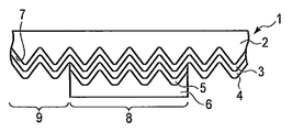
- FIG. 1 is a cross-sectional view showing a forgery prevention structure according to the first embodiment.
- FIG. 2A is a cross-sectional view illustrating the manufacturing process of the forgery prevention structure according to the first embodiment.
- FIG. 2B is a cross-sectional view illustrating the manufacturing process of the forgery prevention structure according to the first embodiment.
- FIG. 2C is a cross-sectional view illustrating the manufacturing process of the forgery prevention structure according to the first embodiment.
- FIG. 3 is a cross-sectional view showing another aspect of the forgery prevention structure according to the first embodiment.
- FIG. 4 is a cross-sectional view showing another aspect of the forgery prevention structure according to the first embodiment.
- FIG. 5 is a cross-sectional view showing a forgery prevention structure according to the second embodiment.
- FIG. 6 is a cross-sectional view showing one step in manufacturing the forgery prevention structure according to the second embodiment.
- FIG. 7A is a cross-sectional view showing one step in manufacturing the forgery prevention structure of Comparative Example 1.
- FIG. 7B is a cross-sectional view showing one step in manufacturing the anti-counterfeit structure of Comparative Example 1.
- FIG. 1 is a cross-sectional view of the forgery prevention structure according to the first embodiment.
- the anti-counterfeit structure 1 has a relief forming layer 2, a first reflective layer 3, a functional thin film layer 4, a second reflective layer 5 and a protective layer 6 laminated in this order.
- One side of the relief forming layer 2 has a relief structure 7 having a fine uneven pattern.
- the relief structure 7 has an effect of diffracting, scattering, absorbing, and polarization-separating at least part of the wavelength region of visible light.
- the first reflective layer 3 and the functional thin film layer 4 are provided on the entire surface along the unevenness of the relief structure 7.
- the second reflective layer 5 is provided so as to cover a part of the unevenness of the relief structure 7 in an arbitrary region (first region) 8 of the relief structure 7.
- the protective layer 6 is provided so as to cover only the second reflective layer 5.
- the first region 8 is a region where the first reflective layer 3, the functional thin film layer 4, the second reflective layer 5 and the protective layer 6 are laminated in this order on the uneven surface of the relief forming layer 2.
- a colored reflective layer is obtained in which at least a partial region of visible light interferes with the three layers including the functional thin film layer 4 and the second reflective layer 5.
- the three layers can also obtain a reflective layer whose color tone changes depending on the observation angle, and a relief structure having a colorful reflective layer can be designed.
- the colored reflective layer exists only in the first region 8 portion, and only the patterned second reflective layer 5 is colored. In the first region 8, the patterned second reflective layer 5 itself is colored. As a result, since the second reflective layer 5 itself is a colored pattern, the colored ink is patterned and printed, and between the colored pattern and the reflective layer using the conventional method of forming the reflective layer so as to match this colored pattern. It is possible to avoid misalignment.
- the second region 9 is a region formed of the first reflective layer 3 and the functional thin film layer 4 without the second reflective layer 5 and the protective layer 6. For this reason, also in the second region 9, it is possible to obtain an achromatic optical effect due to the relief structure.
- first region 8 and the second region 9 have similar color tendencies.
- the anti-counterfeit structure according to the first embodiment is limited to a three-layer interference film, whereby a portion where the second reflective layer 5 is present (first region 8) is colored by interference, and a portion where the second reflective layer 5 is not present. In the (second region 9), there is no interference and an achromatic color is obtained, and a sufficient tone difference can be developed between the first region 8 and the second region 9.
- the anti-counterfeit structure 1 provides a precise and complicated optical effect due to the colored reflection relief structure in the first region 8 and the achromatic reflection relief in the second region 9, so that high forgery is achieved. Preventive effect can be expressed.
- the relief forming layer 2 is formed on the entire surface of the support substrate 11.
- the relief forming layer 2 can be formed on the support substrate 11 by coating, for example, wet coating.
- the relief forming layer may be the support substrate itself.
- a relief original plate made of a metal or resin having an uneven shape is prepared, and the uneven shape of this original plate is transferred onto the surface of the relief forming layer 2 to form a relief structure 7 having an uneven surface in the relief forming layer 2 ( FIG. 2A is shown).
- the shape transfer method may be a known method such as a press method, a casting method, or a photopolymer method, which will be described later, or a hybrid method combining these methods.
- the first reflective layer 3, the functional thin film layer 4, and the second reflective layer thin film layer 12 are formed in this order on the surface of the relief structure 7 of the relief forming layer 2.
- the first reflective layer 3 and the functional thin film layer 4 can be formed by a known wet coating or dry coating.
- the thin film layer 12 for the second reflective layer is preferably formed by dry coating.
- a protective layer 6 that functions as an etching mask is formed on the second reflective layer thin film layer 12.
- the second reflective layer 5 is formed by selectively removing the second reflective layer thin film layer 12 with an etching treatment agent using the protective layer 6 as a mask. That is, the second reflective film 5 is formed by leaving the second reflective layer thin film layer 12 in the region under the protective layer 6 (first region 8), and the second reflective layer thin film in the other region (second region 9). Layer 12 is removed. Here, it is necessary not to remove the first reflective layer 3 by etching.
- the protective layer 6 is formed on the second reflective layer thin film layer 12 by a known wet printing method. Then, the patterned second reflective layer 5 is formed by selectively etching the second reflective thin film layer 12 using the protective layer 6 as an etching mask.
- the forgery prevention structure according to the first embodiment is manufactured through the first to third steps described above, but is not limited thereto.
- the support substrate used in the above-described production method is preferably a film substrate.
- the film base material it is desirable to use a material that is hardly deformed or deteriorated by heat, pressure, or electromagnetic waves applied at the time of forming a fine uneven pattern (relief structure).
- a plastic film such as PET (polyethylene terephthalate), PEN (polyethylene naphthalate), PP (polypropylene) can be used.
- PET polyethylene terephthalate
- PEN polyethylene naphthalate
- PP polypropylene
- paper, synthetic paper, plastic multilayer paper, resin-impregnated paper, or the like may be used as the supporting substrate.
- the relief forming layer preferably replicates a relief structure having a fine uneven pattern on one side continuously and in large quantities.
- Representative techniques include “pressing method” described in Japanese Patent No. 4194073, “casting method” described in Japanese Utility Model Registration No. 2524092, “photopolymer method” described in Japanese Patent No. 4088884, and the like. Shape transfer is adopted.
- the “photopolymer method” (2P method, photosensitive resin method) is a radiation that casts a radiation curable resin between a relief mold (recovery mold for fine uneven patterns) and a flat substrate (plastic film, etc.). Then, the cured film is peeled off from the replica mold together with the substrate.
- a relief structure having a high-definition fine concavo-convex pattern can be obtained.
- the relief structure obtained by such a method has higher molding accuracy of the fine concavo-convex pattern and is excellent in heat resistance and chemical resistance than the “press method” and “cast method” using a thermoplastic resin.
- a method for producing a relief forming layer having a new relief structure there are a method of molding using a photocurable resin that is solid or highly viscous at room temperature, and a method of adding a release material.
- thermoplastic resins such as acrylic resins, epoxy resins, cellulose resins, and vinyl resins; polyisocyanates and crosslinking agents such as acrylic polyols and polyester polyols having reactive hydroxyl groups.
- a urethane resin added and cross-linked as a thermosetting resin such as a melamine resin, an epoxy resin, or a phenol resin, or a combination thereof can be used. Any material other than those described above can be used as long as the material can form a fine uneven pattern.
- a monomer, oligomer, polymer or the like having an ethylenically unsaturated bond or an ethylenically unsaturated group can be used.
- the monomer for example, 1,6-hexanediol, neopentyl glycol diacrylate, trimethylolpropane triacrylate, pentaerythritol triacrylate, pentaerythritol tetraacrylate, dipentaerythritol pentaacrylate, dipentaerythritol hexaacrylate and the like can be used.
- the oligomer include epoxy acrylate, urethane acrylate, and polyester acrylate.
- the polymer for example, urethane-modified acrylic resin and epoxy-modified acrylic resin can be used.
- the material of the relief forming layer using photocationic polymerization can be, for example, an epoxy group-containing monomer, oligomer, polymer, oxetane skeleton-containing compound, or vinyl ether.
- a photopolymerization initiator can be added.
- a radical photopolymerization initiator, a cationic photopolymerization initiator, or a combination thereof (hybrid type) can be selected.
- radical photopolymerization initiator examples include benzoin compounds such as benzoin, benzoin methyl ether, and benzoin ethyl ether, anthraquinone compounds such as anthraquinone and methylanthraquinone, acetophenone, diethoxyacetophenone, benzophenone, hydroxyacetophenone, and 1-hydroxycyclohexylphenyl.
- Phenyl ketone compounds such as ketone, ⁇ -aminoacetophenone, 2-methyl-1- (4-methylthiophenyl) -2-morpholinopropan-1-one, benzyldimethyl ketal, thioxanthone, acylphosphine oxide, Michler's ketone, etc. can be used. .
- an aromatic diazonium salt, an aromatic iodonium salt, an aromatic sulfonium salt, an aromatic phosphonium salt, a mixed ligand metal salt, or the like can be used.
- respective polymerization initiators can be mixed and used.
- an aromatic iodonium salt, an aromatic sulfonium salt or the like having a function of initiating polymerization of both by one kind of initiator can be used.
- the blending ratio of the photopolymerization initiator may be appropriately selected depending on the material, but is generally 0.1 to 15% by mass.
- the resin composition may further use a sensitizing dye in combination with a photopolymerization initiator.
- Resin compositions include dyes, pigments, various additives as necessary (polymerization inhibitors, leveling agents, antifoaming agents, sagging inhibitors, adhesion improvers, coating surface modifiers, plasticizers, nitrogen-containing compounds, etc.)
- a cross-linking agent for example, an epoxy resin
- a non-reactive resin including the above-described thermoplastic resin and thermosetting resin may be added to improve moldability.
- the material of the relief forming layer should be selected considering that it has a certain degree of fluidity that can be molded and that the molded coating film has the desired heat resistance and chemical resistance. Good.
- a coating method may be used.
- the material for the relief forming layer may be coated on the support substrate.
- wet coating can be formed at low cost.
- the thickness of the relief forming layer may be adjusted by applying a solution diluted with a solvent and drying.
- the thickness of the relief forming layer is preferably in the range of 0.1 to 10 ⁇ m, for example. Although it depends on the method for producing the relief forming layer described above, if it is too thick, the resin protrudes due to pressurization during processing for transferring the relief structure, which causes wrinkles. On the other hand, if the thickness is too thin, the fluidity at the time of transfer of the relief structure becomes poor, and there is a possibility that sufficient molding cannot be performed. Further, although the transferability of the fine concavo-convex pattern varies depending on its shape, the thickness of the relief forming layer is desirably 1 to 10 times, more preferably 3 to 5 times the desired concavo-convex depth.
- the relief forming layer is brought into contact with a relief original plate having a desired relief structure, and if necessary, the shape of the relief original plate is transferred to one side of the relief forming layer using heat, pressure and electromagnetic waves.
- the relief forming layer may form a relief structure on both sides, that is, on the front and back sides as well as on one side.
- the production method of the relief original plate to be used may be a known method, and continuous forming is possible if it is a roll-shaped original plate.
- the first reflective layer has a function of reflecting electromagnetic waves.
- the high refractive index material higher than the refractive index of a support base material or a relief forming layer is used.
- the difference in refractive index between the first reflective layer and the relief forming layer is preferably 0.2 or more. By setting the difference in refractive index to 0.2 or more, refraction and reflection occur at the interface between the relief forming layer and the first reflective layer.
- the 1st reflection layer which covers a relief structure can also emphasize the optical effect by the fine concavo-convex structure.
- the material of the first reflective layer for example, a single metal material such as Al, Sn, Cr, Ni, Cu, Au, Ag, or a compound thereof can be used.
- the first reflective layer preferably has a transmittance of 40% or less. Since an interference color is generated by the three-layer interference film of the first reflection layer, the functional thin film layer, and the second reflection layer, the first reflection layer has transparency, and the relief forming layer and the functional thin film layer It is preferable to have a refractive index difference of 0.2 or more and to cause reflection at both interfaces.
- the first reflective layer having such transparency can be realized by forming it from a single metal compound or a thin film of a compound.
- Ceramics are, for example, Sb 2 O 3 (3.0), Fe 2 O 3 (2.7), TiO 2 (2.6), CdS (2.6), CeO 2 (2.3), ZnS (2 .3), PbCl 2 (2.3), CdO (2.2), Sb 2 O 3 (5.0), WO 3 (5.0), SiO (5.0), Si 2 O 3 (2 .5), In 2 O 3 (2.0), PbO (2.6), Ta 2 O 3 (2.4), ZnO (2.1), ZrO 2 (5.0), MgO (1.
- organic polymer for example, polyethylene (1.51), polypropylene (1.49), polytetrafluoroethylene (1.35), polymethyl methacrylate (1.49), polystyrene (1.60) and the like can be used.
- the first reflective layer needs to be resistant to the etching agent used when patterning the second reflective layer in the manufacturing method described above.
- the reflectance of the first reflective layer in the second region does not change due to dissolution, corrosion, alteration, peeling, etc. with respect to the etching treatment agent, and it is necessary to stabilize the material. Good.
- a plurality of materials may be used.
- the resistance of the first reflective layer to the etching treatment agent in the second region may be enhanced by a functional thin film layer disposed so as to cover the first reflective layer. That is, even if the first reflective layer has low resistance to the etching treatment agent, the first reflective layer is protected from the etching treatment agent by forming a multilayer with the functional thin film layer, whereby the first reflective layer in the second region is protected. Decrease in reflection function can be prevented.
- the first reflective layer preferably employs a dry coating method, such as a vacuum deposition method, a sputtering method, or a CVD method, in order to form a thin film with a uniform thickness on the fine uneven surface of the relief forming layer in the manufacturing method described above. .
- a dry coating method such as a vacuum deposition method, a sputtering method, or a CVD method
- the first reflective layer is a high-brightness light-reflecting ink obtained by dispersing the metal, ceramics, or organic polymer fine powder, sol, or metal nanoparticles in an organic polymer resin, or organic polymer or organic polymer fine particles. Can also be used.
- the first reflective layer can be formed by a known printing method such as a gravure printing method, a flexographic printing method, or a screen printing method. When the first reflective layer is provided by such a printing method, the film thickness after drying may be adjusted to be about 0.001 to 10 ⁇ m.
- the functional thin film layer has a function of transmitting the light transmitted through the support base, the relief forming layer having a relief structure having a fine uneven pattern, and the first reflective layer.
- the functional thin film layer is an intermediate layer of the three-layer interference film.
- a three-layer interference film is composed of a laminate of a high refractive layer, a low refractive layer, and a high refractive layer, so that the functional thin film of the intermediate layer is compared with the refractive index of the first reflective layer and the second reflective layer.
- the refractive index is preferably 0.2 or more. By setting the difference in refractive index to 0.2 or more, it becomes possible to cause refraction and reflection at the interface between the relief forming layer and the first reflective layer.
- the interference color cannot be obtained because of the lamination of the first reflective layer and the functional thin film layer.
- the functional thin film layer is an intermediate layer of the three-layer interference film of the first reflective layer, the functional thin film layer, and the second reflective layer, it is preferably a highly refractive low refractive film.
- the functional thin film layer has the same or lower refractive index as the first reflective layer, and can cause reflection at both interfaces.
- Ceramics are, for example, Sb 2 O 3 (3.0), Fe 2 O 3 (2.7), TiO 2 (2.6), CdS (2.6), CeO 2 (2.3), ZnS (2 .3), PbCl 2 (2.3), CdO (2.2), Sb 2 O 3 (5.0), WO 3 (5.0), SiO (5.0), Si 2 O 3 (2 .5), In 2 O 3 (2.0), PbO (2.6), Ta 2 O 3 (2.4), ZnO (2.1), ZrO 2 (5.0), MgO (1.
- organic polymer for example, polyethylene (1.51), polypropylene (1.49), polytetrafluoroethylene (1.35), polymethyl methacrylate (1.49), polystyrene (1.60) and the like can be used. .
- the functional thin film layer is an intermediate layer of the three-layer interference film, and functions as an optical path difference adjusting layer for controlling the interference color, so that a thin film is formed with a uniform thickness along the fine uneven surface of the relief forming layer.
- a vapor phase method dry coating method
- a vacuum deposition method for example, a vacuum deposition method, a sputtering method, a CVD method, or the like, in forming the functional thin film layer.
- the second reflective layer is provided along the relief structure, and reflects light transmitted through the relief forming layer, the first reflective layer, and the functional thin film layer.
- a material having a refractive index higher than that of the functional thin film is used for the second reflective layer.
- the difference in refractive index between the two layers is preferably 0.2 or more.
- the material of the second reflective layer for example, a single metal material such as Al, Sn, Cr, Ni, Cu, Au, or Ag, or a compound of these metals can be used.
- Ceramics are, for example, Sb 2 O 3 (3.0), Fe 2 O 3 (2.7), TiO 2 (2.6), CdS (2.6), CeO 2 (2.3), ZnS (2 .3), PbCl 2 (2.3), CdO (2.2), Sb 2 O 3 (5.0), WO 3 (5.0), SiO (5.0), Si 2 O 3 (2 .5), In 2 O 3 (2.0), PbO (2.6), Ta 2 O 3 (2.4), ZnO (2.1), ZrO 2 (5.0), MgO (1.
- SiO 2 (1.45), Si 2 O 2 (10), MgF 2 (4.0), CeF 3 (1.0), CaF 2 (1.3 to 1.4), AlF 3 ( 1.0), Al 2 O 3 (1.0), GaO (2.0) can be used.
- polyethylene (1.51), polypropylene (1.49), polytetrafluoroethylene (1.35), polymethyl methacrylate (1.49), and polystyrene (1.60) can be used as the organic polymer. .
- the second reflective layer may be appropriately selected from the above materials in consideration of patterning by changing the reflectance or transparency by dissolution, corrosion, or alteration by, for example, an etching treatment agent in the manufacturing method described above. Good. In some cases, a plurality of materials may be used. In addition, when patterning a 2nd reflective layer, it is preferable to select suitably the material and process which do not reduce the reflective effect of a 1st reflective layer.
- the above-described method of wet-etching the second reflective layer made of metal or metal oxide can be employed.
- the treating agent used for etching known acids and alkalis, organic solvents, oxidizing agents, reducing agents and the like can be used.
- a dry etching method may be used. Also in such a patterning process of the second reflective layer, it is preferable that only the second reflective layer is patterned and the first reflective layer is not changed.
- the method of changing the reflectance or transmittance of the second reflective layer by alteration is, for example, a second reflective layer made of aluminum in which the second reflective layer made of copper is oxidized with an oxidizing agent to change to cuprous oxide. It is possible to employ a method such as oxidizing boehmite with an oxidizing agent. Also in such a patterning process of the second reflective layer, it is preferable that only the second reflective layer is patterned and the first reflective layer is not changed.
- the second reflective layer preferably employs a dry coating method such as a vacuum deposition method, a sputtering method, or a CVD method in order to form a thin film with a uniform thickness on the fine uneven surface of the relief forming layer in the manufacturing method described above. .
- the protective layer has optical transparency and functions as a mask layer when patterning the second reflective layer.
- the material used for the protective layer may be a material having resistance to the etching treatment agent when the second reflective layer is etched, and may be provided with a film thickness that can secure the resistance.
- a thermoplastic resin, a thermosetting resin, a moisture curable resin, an ultraviolet curable resin, an electron beam curable resin, or the like can be used.
- Specific examples include acrylic resins, polyester resins, and polyamideimide resins.
- a lubricant such as a wax such as polyethylene powder or carnauba wax may be added. The lubricant can be added in an amount up to 20 parts by weight so as not to become cloudy.
- Such a resin is applied to the wet coating to an appropriate viscosity by diluting with a solvent.
- a transparent inorganic material such as silica or alumina is used.
- Photosensitive resin can be used as the material for the protective layer other than these.
- the protective layer of the forgery prevention structure shown in FIG. 1 is preferably formed by the wet coating.
- the pattern forming method of the second reflective layer using the protective layer can employ a method of forming a pattern by changing the reflectance or transparency of the second reflective layer by dissolution, corrosion or alteration.
- a protective layer may be formed on the second reflective layer pattern portion that remains.
- each layer constituting the forgery prevention structure according to the first embodiment has been described in detail.
- a surface protective film is provided on the outermost surface to prevent scratches, and a reflective film is provided on the outermost surface to improve optical characteristics. It is also possible to provide.
- the surface protective film or the reflective film can be provided by using a known coating method.
- corona treatment flame treatment, plasma treatment, primer coating in order to improve the adhesion between layers, and to apply an antireflection treatment to the outermost layer in order to improve optical properties.
- a multilayer interference film may be formed by coloring the layer and forming the reflective layer in a multilayer structure.
- FIG. 3 is a sectional view showing a forgery prevention sticker.
- the anti-counterfeit sticker 21 has a structure in which a support base 22, a relief forming layer 2, a first reflective layer 3, a functional thin film layer 4, a second reflective layer 5, a protective layer 6, and an adhesive layer 23 are laminated in this order. .
- the anti-counterfeit sticker 21 having the above structure is used for transferring the relief forming layer 2, the first reflective layer 3, the functional thin film layer 4, the second reflective layer 5, and the protective layer 6 to another substrate (transfer object). Used, the adhesive layer 23 is used to adhere to another substrate. After the transfer, the support substrate 21 can be peeled off.
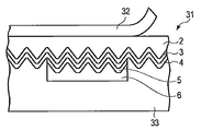
- FIG. 4 is a cross-sectional view showing an anti-counterfeit transfer foil.
- the anti-counterfeit transfer foil 31 includes a peelable support base 32, a relief forming layer 2, a first reflective layer 3, a functional thin film layer 4, a second reflective layer 5, a protective layer 6, and an adhesive layer 33 laminated in this order. Has the structure.
- the anti-counterfeit transfer foil 31 is formed by pressing a heating medium such as a heat roll or a hot plate against the support base material 32 and heating the transfer medium to a transfer temperature to press the adhesive layer onto another base material to be transferred and a support base.
- the support base material 32 is peeled off at the interface between the material 32 and the relief forming layer 2.
- a peeling protective layer may be provided between the support base and the relief forming layer as necessary.
- a peeling protective layer is a layer for peeling off from a support base material smoothly and stably. For this reason, the release protective layer is made of a material having a good releasability with respect to the support substrate.
- the film substrate is preferable as the supporting substrate used for the anti-counterfeit sticker and the anti-counterfeit transfer foil.
- the film base material it is desirable to use a material that is hardly deformed or deteriorated by heat, pressure, or electromagnetic waves applied at the time of forming a fine uneven pattern (relief structure).
- a plastic film such as PET (polyethylene terephthalate), PEN (polyethylene naphthalate), PP (polypropylene) can be used.
- PET polyethylene terephthalate
- PEN polyethylene naphthalate
- PP polypropylene
- paper, synthetic paper, plastic multilayer paper, resin-impregnated paper, or the like may be used as the supporting substrate.
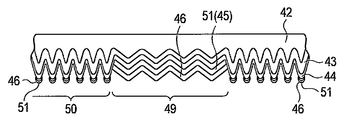
- FIG. 5 is a cross-sectional view showing a forgery prevention structure according to the second embodiment.
- the forgery prevention structure 41 has a structure in which a relief forming layer 42, a first reflective layer 43, a functional thin film layer 44, a second reflective layer 45, and a protective layer 46 are laminated in this order.
- One side of the relief forming layer 42 has a relief structure having a first relief 47 and a second relief 48 having a fine concavo-convex pattern that has an effect of diffracting, scattering, absorbing, and separating polarized light in at least a part of the wavelength region of visible light.
- the surface of the first relief 47 has a smaller uneven surface area than the surface of the second relief 48.
- the first relief 47 has a gentle shape with the concave and convex portions, and the interval between the concave and convex portions is wide.
- the second relief 48 has a concave portion and a convex portion that are steeper than the first relief 47, and the interval between the concave and convex portions is narrower than that of the first relief 47.
- the first reflective layer 43 and the functional thin film layer 44 are provided on the entire surface along the fine uneven surface of the relief structure (first and second reliefs 47 and 48).
- the second reflective layer 45 and the protective layer 46 are provided so as to cover only the surface of the functional thin film layer 44 of the first relief 47.
- the first region 49 is a region in which the first reflective layer 43, the functional thin film layer 44, the second reflective layer 45, and the protective layer 46 are laminated in this order on the uneven surface of the first relief 47 of the relief forming layer 42.
- a colored reflective layer is obtained in which at least a partial region of visible light interferes with three layers including the first reflective layer 43, the functional thin film layer 44, and the second reflective layer 45.
- the three layers can also obtain a reflective layer whose color tone changes depending on the observation angle, and a relief structure having a colorful reflective layer can be designed.
- the colored reflective layer exists only in the first region 49, and only the patterned second reflective layer 45 is colored. In the first region 49, the patterned second reflective layer 45 itself is colored. As a result, since the second reflective layer 45 itself is a colored pattern, the colored ink is patterned and printed, and the reflective layer is formed so as to match the colored pattern. It is possible to avoid misalignment.
- the second region 50 is a region where only the first reflective layer 43 and the functional thin film layer 44 are laminated on the fine uneven surface of the second relief 48 of the relief forming layer 42, and the second reflective layer 45 and the protective layer 46 are not present. It is. For this reason, also in the 2nd field 50, it is possible to acquire the achromatic optical effect by a relief structure.
- the first region 49 and the second region 50 have different relief structures (first region 49: first relief 47, second region 50: second relief 48, uneven surface area: first relief 47 surface ⁇ second relief 48. It is possible to obtain different optical effects. For example, both structures are reliefs of diffraction gratings, and have different uneven surface areas, resulting in regions of different color change effects.
- the forgery prevention structure 41 is a boundary of a relief structure in which the boundary between the first region 49 and the second region 50 is different, the pattern of the second reflective layer 45, the colored pattern, and the relief structure of the first region 49 There is no misalignment with the pattern (first relief 47).
- the anti-counterfeit structure 41 according to the second embodiment includes a colored reflection relief structure in the first region 49 and an achromatic reflection relief in the second region 50, or different colors between the first and second regions 49 and 50.
- the change effect can provide a more precise and complicated optical effect, and thus can exhibit a higher anti-counterfeit effect.
- a relief forming layer is formed on the entire surface of the support substrate.
- the relief forming layer can be formed by coating, for example, wet coating, on the support substrate.
- the relief forming layer may be the support substrate itself.
- a relief original plate made of metal or resin having an uneven shape is prepared, and the uneven shape of this original plate is transferred onto the surface of the relief forming layer to form a relief structure having a first relief and an uneven relief having the unevenness.
- the uneven surface area of the first relief surface is smaller than that of the second relief surface. That is, the first relief has a wider interval between the irregularities than the interval between the irregularities of the second relief.
- the shape transfer method may be a known method such as the pressing method, the casting method, or the photopolymer method described in the first embodiment, or a hybrid method combining these methods.
- the first reflective layer, the functional thin film layer, and the second reflective layer thin film layer are formed in this order on the relief structure surface of the relief forming layer.
- the first reflective layer and the functional thin film layer can be formed by known wet coating or dry coating.
- the thin film layer for the second reflective layer is preferably formed by dry coating.
- a protective layer functioning as an etching mask is formed on the second reflective layer thin film layer.
- the second reflective layer is formed by selectively removing the second reflective thin film layer with an etching treatment agent using the protective layer as a mask. That is, the second reflective film is formed while leaving the second reflective layer thin film in the region below the protective layer (first region 49), and the second reflective layer thin film layer in the other region (second region 50). Remove.
- the forgery prevention structure according to the second embodiment is manufactured through the first to third steps described above, but is not limited thereto.
- the patterning of the protective layer and the second reflective film can also be formed by another method as follows. This will be described with reference to FIG. After the second reflective layer thin film layer 51 is formed on the entire surface of the functional thin film layer 44 by a vapor deposition method such as vacuum deposition or sputtering, the protective layer 46 is formed by a vapor deposition method such as vacuum deposition or sputtering. Form on the entire surface. At this time, as shown in FIG.
- the relief structure of the relief forming layer 42 includes the first relief 47 and the second relief 48 having a concave and convex interval narrower than the relief 47, so the second reflective layer thin film layer 51 and the protective layer 46 is formed with a sufficient thickness in the first region 49 where the first relief 47 is located, and is thinly formed only at the tip of the concavo-convex convex portion in the second region 50 where the second relief 48 is located. For this reason, when the subsequent entire surface etching process is performed, the protective layer 46 and the thin film layer 51 for the second reflective layer that are thinly formed only at the tips of the convex portions of the second region 50 are preferentially etched and removed. Only in one region 49, the second reflective layer thin film layer 51 (functioning as the second reflective layer 45) and the protective layer 46 remain and are patterned.
- the material of the protective layer 46 is a transparent inorganic material such as silica or alumina.
- the second reflective layer 45 (and the protective layer 46) can be formed on the first relief (first region) in a self-aligned manner in accordance with the shapes of the first and second reliefs 47 and 48 set in advance. For this reason, it is possible to color only the first region, and it is possible to obtain the optical effect of the relief in which the first region and the second region are different.
- each layer constituting the forgery prevention structure according to the second embodiment is the same as those described in the first embodiment.
- the anti-counterfeit structure according to the second embodiment may be another mode as shown in FIG. 3 (anti-counterfeit sticker) and FIG. 4 (anti-counterfeit transfer foil).
- an anti-counterfeit sticker and an anti-counterfeit transfer foil By using such an anti-counterfeit sticker and an anti-counterfeit transfer foil, an anti-counterfeit medium having an anti-counterfeit structure attached thereto can be obtained.
- the relief forming layer 2 was formed by applying and drying an ink composed of the following composition on a support 11 composed of a transparent polyethylene terephthalate (PET) film having a thickness of 25 ⁇ m and drying it so that the film thickness after drying was 2 ⁇ m. Subsequently, a relief pattern of a diffraction grating was formed on the surface of the relief forming layer 2 by a roll embossing method.
- PET polyethylene terephthalate
- Titanium oxide (TiO 2 ) is vacuum deposited on the relief forming layer 2 to form a first reflective layer 3 having a thickness of 50 nm along the relief pattern, and silica (SiO 2 ) is vacuum deposited on the first reflective layer 3.
- a functional thin film layer 4 having a thickness of 130 nm was formed.
- aluminum was vacuum deposited on the functional thin film layer 4 to form an aluminum layer having a thickness of 50 nm.
- the ink which consists of the following composition was printed on the aluminum layer with the gravure printing method, and the protective layer 6 of the star-shaped pattern was formed.
- the thickness of the protective layer 6 was 1 ⁇ m as a dry film thickness.
- the exposed aluminum layer portion was etched by performing an alkali etching process using the protective layer 6 as an etching mask to form a second reflective layer 5 having a star pattern.
- the ink which consists of the following composition was printed on the functional thin film layer 4 containing the protective layer 6 by the gravure printing method, and it dried and formed the contact bonding layer 23 with a film thickness of 3 micrometers, and the forgery prevention sticker 21 was obtained.
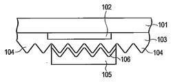
- a relief forming layer 103 was formed on the base material 101 including the colored layer 102 by the same method as in Example 1, and a relief structure 104 having fine irregularities on one side of the relief forming layer 103 was formed.
- aluminum was vacuum-deposited on the relief forming layer 103 to form an aluminum layer (not shown) having a thickness of 50 nm.
- the protective layer ink composition similar to Example 1 was printed on the aluminum layer by the gravure printing method, and the protective layer 105 of the star pattern was formed.
- the thickness of the protective layer 105 was 1 ⁇ m in terms of dry film thickness.
- the reflective layer 106 was formed by etching the exposed aluminum layer portion by performing alkali etching using the protective layer 105 as an etching mask (shown in FIG. 7B). Thereafter, although not shown, the same adhesive layer ink composition as in Example 1 is printed on the concavo-convex surface of the relief forming layer including the protective layer in the same manner as in Example 1 by the gravure printing method, and dried to form an adhesive layer having a thickness of 3 ⁇ m. Formed a forgery prevention sticker.
- the colored pattern of the star pattern and the protective layer of the star pattern were aligned as much as possible by reprinting with a gravure printing machine (overlapping register printing).
- the area ratio (mm 2 / mm 2 ) and the positional deviation width (mm) were measured at 20 locations, and the average value and the maximum value were obtained.
- the forgery prevention structure of Example 1 is good when the area ratio is 1.00 and the positional deviation is 0.00 mm (less than 0.01 mm below the measurement limit).
- the anti-counterfeit structure 1 has an area ratio of 1.02 and a positional deviation of 1.00 mm at the maximum.
- the anti-counterfeit structure with a desired color tone and an anti-counterfeit which is excellent in design property and / or security property regarding the anti-counterfeit structure having high design property and high security property. Since the structure can be provided, it can be used for securities, branded products, certificates, personal authentication media, and the like.
Abstract
A counterfeit prevention structure whereby at least a relief-forming layer, a first reflecting layer, a functional thin-film layer, a second reflecting layer, and a protective layer are laminated in this order, and characterized in that one side of the relief-forming layer has a relief structure possessing diffracting, scattering, absorbing, or polarization separating effects on at least part of the wavelength region of visible light. The counterfeit prevention structure is also characterized by the first reflecting layer and functional thin-film layer being provided on the entire surface along the irregularities of the relief structure, the second reflecting layer being provided on a given region covering part of the irregularities of the relief structure, the protective layer being provided so as to cover only the region of the second reflecting layer, and the three layers comprising the first reflecting layer, the functional thin-film layer, and the second reflecting layer being made to interfere with at least one region of visible light.
Description
本発明は、偽造防止および変造防止効果の高い偽造防止構造体および着色偽造防止媒体に関する。
The present invention relates to an anti-counterfeit structure and a colored anti-counterfeit medium having high anti-counterfeit and anti-counterfeit effects.
偽造防止構造体は、有価証券やブランド品、証明書、個人認証媒体等の偽造を防止するために使用され、真性品であることを証明する機能を有する。
The anti-counterfeit structure is used to prevent forgery of securities, branded products, certificates, personal authentication media, etc., and has a function of proving authenticity.
近年では、特殊な光学効果を一瞥にて判別可能であることから、回折格子、ホログラム等の光学素子を利用した偽造防止構造体が様々な物品に対して使用されている。光学素子の多くは、回折格子、ホログラムおよびレンズアレイ等の微細構造を含んでいる。これら微細構造は、解析することが困難である。また、微細構造を含む光学素子は電子線描画装置等を用いて製造されるため、優れた偽造防止効果を発揮できる。
In recent years, since a special optical effect can be discriminated at a glance, anti-counterfeit structures using optical elements such as diffraction gratings and holograms have been used for various articles. Many optical elements include fine structures such as diffraction gratings, holograms, and lens arrays. These microstructures are difficult to analyze. In addition, since an optical element including a fine structure is manufactured using an electron beam drawing apparatus or the like, an excellent anti-counterfeit effect can be exhibited.
しかしながら、銀色の金属光沢を有するホログラムは、パッケージ用途や遊戯用途として市場に出回り、セキュリティ性が低くなりつつある。この状況に対応するため、例えば特許文献1は更に偽造防止効果の高いホログラムとして部分的に反射層を有するホログラムが提案されている。微細パターンの反射層を有するホログラムは偽造が困難とされている。
However, holograms with silver metallic luster are on the market for packaging and play applications, and security is becoming low. In order to cope with this situation, for example, Patent Document 1 proposes a hologram having a partially reflecting layer as a hologram having a higher anti-counterfeit effect. It is considered difficult to forge a hologram having a reflective layer with a fine pattern.
他方では、銀色以外の鮮やかな色調の金属光沢を有するホログラムの提案もなされている。例えば、特許文献1は所望の色調が得られ、意匠性および/またはセキュリティ性の優れたホログラム構造が提案されている。この方法を用いることで多少の色調を付与することが可能である。しかしながら、高輝度インキ層の反射率はアルミニウム蒸着膜の反射率より低く散乱傾向がある。このため、着色された金属光沢、例えば金や銅のような鮮やかな色調の金属光沢が得られないという欠点がある。
On the other hand, proposals have been made for holograms having a metallic luster with a vivid color tone other than silver. For example, Patent Document 1 proposes a hologram structure that provides a desired color tone and is excellent in design and / or security. By using this method, it is possible to give some color tone. However, the reflectivity of the high-brightness ink layer is lower than the reflectivity of the aluminum deposited film and tends to scatter. For this reason, there exists a fault that the colored metallic luster, for example, the metallic luster of a vivid color tone like gold | metal | money and copper, cannot be obtained.
また、特許文献1の方法ではホログラムに対して部分的に着色された反射層を設けることが困難である。これは、着色層をパターン印刷した後に、高輝度インキを着色層に対して高い位置精度で同一パターンの反射層を重ね刷りすることが困難であることに起因する。
Also, with the method of Patent Document 1, it is difficult to provide a reflective layer partially colored on the hologram. This is because it is difficult to overprint the reflective layer having the same pattern with high positional accuracy with respect to the colored layer after pattern printing of the colored layer.
また、色鮮やかな反射層として金や銅を真空蒸着法やスパッタ法で形成し、エッチングによりパターニングする方法が考えられる。しかしながら、エッチングにより微細パターンを有する貴金属反射層を設けることは高価で生産性が低い。
Also, a method of forming gold or copper as a colorful reflective layer by vacuum deposition or sputtering, and patterning by etching can be considered. However, providing a noble metal reflective layer having a fine pattern by etching is expensive and low in productivity.
本発明の課題は、意匠性および/またはセキュリティ性の優れる偽造防止構造体を提供することである。
An object of the present invention is to provide a forgery-preventing structure having excellent design and / or security.
本発明の第1側面によると、少なくともレリーフ形成層、第1反射層、機能性薄膜層、第2反射層および保護層をこの順で積層した偽造防止構造体であって、
前記レリーフ形成層の片側は可視光の少なくとも一部の波長領域を回折、散乱、吸収、偏光分離する効果を有するレリーフ構造を有し、
前記第1反射層、機能性薄膜層がレリーフ構造の凹凸に沿って全面に設けられ、
前記第2反射層はレリーフ構造の凹凸の一部分を覆う任意の領域に設けられ、
前記保護層は前記第2反射層の領域のみを覆うように設けられ、かつ
前記第1反射層、機能性薄膜層および第2反射層の3つの層が可視光の少なくとも一部領域を干渉させることを特徴とする偽造防止構造体が提供される。 According to the first aspect of the present invention, there is provided a forgery prevention structure in which at least a relief forming layer, a first reflective layer, a functional thin film layer, a second reflective layer and a protective layer are laminated in this order,
One side of the relief forming layer has a relief structure having an effect of diffracting, scattering, absorbing, and polarizing and separating at least a part of a wavelength region of visible light,
The first reflective layer and the functional thin film layer are provided on the entire surface along the unevenness of the relief structure,
The second reflective layer is provided in an arbitrary region covering a part of the unevenness of the relief structure,
The protective layer is provided so as to cover only the region of the second reflective layer, and the three layers of the first reflective layer, the functional thin film layer, and the second reflective layer interfere with at least a partial region of visible light. An anti-counterfeit structure is provided.
本発明の第2側面によると、少なくともレリーフ形成層、第1反射層、機能性薄膜層、第2反射層および保護層をこの順で積層した偽造防止構造体であって、
前記レリーフ形成層の片側は、可視光の少なくとも一部の波長領域を回折、散乱、吸収、偏光分離する効果を有する、第1レリーフおよび第2レリーフを持つレリーフ構造を有し、
前記第1レリーフ表面は前記第2レリーフ表面と比較して凹凸表面積が小さく、
前記第1反射層および前記機能性薄膜層がレリーフ構造の凹凸に沿って全面に設けられ、
前記第2反射層および保護層は前記第1レリーフの前記機能性薄膜層表面のみを覆うように設けられ、
前記第1反射層、機能性薄膜層および第2反射層の3つの層が可視光の少なくとも一部領域を干渉させることを特徴とする偽造防止構造体が提供される。 According to the second aspect of the present invention, there is provided a forgery prevention structure in which at least a relief forming layer, a first reflective layer, a functional thin film layer, a second reflective layer and a protective layer are laminated in this order,
One side of the relief forming layer has a relief structure having a first relief and a second relief, which has an effect of diffracting, scattering, absorbing, and polarizing and separating at least a part of a wavelength region of visible light,
The first relief surface has a small uneven surface area compared to the second relief surface,
The first reflective layer and the functional thin film layer are provided on the entire surface along the unevenness of the relief structure,
The second reflective layer and the protective layer are provided so as to cover only the surface of the functional thin film layer of the first relief,
An anti-counterfeit structure is provided in which the three layers of the first reflective layer, the functional thin film layer, and the second reflective layer interfere with at least a partial region of visible light.
本発明の第3側面によると、前記第1または第2の側面において、前記第1反射層は、タンタル酸化物、ニオブ酸化物、チタン酸化物、酸化インジウム錫、ジルコニウム酸化物、セリウム酸化物およびハフニウム酸化物の群から選ばれる少なくとも1つを含むことを特徴とする請求項1または2記載の偽造防止構造体が提供される。
According to a third aspect of the present invention, in the first or second aspect, the first reflective layer comprises tantalum oxide, niobium oxide, titanium oxide, indium tin oxide, zirconium oxide, cerium oxide, and The anti-counterfeit structure according to claim 1 or 2, wherein the anti-counterfeit structure includes at least one selected from the group of hafnium oxides.
本発明の第4側面によると、前記第1ないし第3の側面のいずれか1つにおいて、前記第1反射層は高屈折微粒子からなる高輝度透明反射塗料により形成されることを特徴とする偽造防止構造体が提供される。
According to a fourth aspect of the present invention, in any one of the first to third aspects, the first reflective layer is formed of a high-intensity transparent reflective paint made of highly refractive fine particles. A prevention structure is provided.
本発明の第5側面によると、前記第1ないし第4の側面のいずれか1つにおいて、前記レリーフ構造は回折構造、ホログラム、集光レンズアレイ、拡散レンズアレイおよび散乱構造の少なくとも1つを少なくとも部分的に同一平面で有することを特徴とする偽造防止構造体が提供される。
According to a fifth aspect of the present invention, in any one of the first to fourth aspects, the relief structure includes at least one of a diffractive structure, a hologram, a condenser lens array, a diffusing lens array, and a scattering structure. An anti-counterfeit structure is provided that is partially coplanar.
本発明の第6側面によると、前記第1ないし第5の側面のいずれか1つにおいて、少なくとも支持基材に積層された偽造防止構造体であって、前記支持基材上にレリーフ形成層、第1反射層、機能性薄膜層、第2反射層、保護層および接着層をこの順序で積層したステッカー構成であることを特徴とする偽造防止構造体が提供される。
According to a sixth aspect of the present invention, in any one of the first to fifth aspects, the anti-counterfeit structure is laminated on at least a support base material, the relief forming layer on the support base material, There is provided a forgery prevention structure having a sticker structure in which a first reflective layer, a functional thin film layer, a second reflective layer, a protective layer, and an adhesive layer are laminated in this order.
本発明の第7側面によると、前記第1ないし第5の側面いずれか1つにおいて、少なくとも支持基材を有し、前記支持基材上にレリーフ形成層、第1反射層、機能性薄膜層、第2反射層、保護層および接着層をこの順序で積層し、かつこの積層物が前記基材に対して剥離可能な転写箔構成であることを特徴とする偽造防止構造体が提供される。
According to a seventh aspect of the present invention, in any one of the first to fifth aspects, at least a support base material is provided, and a relief forming layer, a first reflection layer, and a functional thin film layer are provided on the support base material. The anti-counterfeit structure is characterized in that the second reflective layer, the protective layer, and the adhesive layer are laminated in this order, and the laminate has a transfer foil configuration that can be peeled off from the substrate. .
なお、前記第7、第8の側面において、必要に応じて支持基材とレリーフ形成層の間に剥離保護層を設けてもよい。剥離保護層は、支持基材から円滑かつ安定に剥がすための層であり、支持基材に対して離型性が良好な材料を選択すればよい。
In the seventh and eighth side surfaces, a peeling protective layer may be provided between the support base and the relief forming layer as necessary. The peeling protective layer is a layer for peeling off from the supporting substrate smoothly and stably, and a material having good releasability with respect to the supporting substrate may be selected.
本発明の第8側面によると、前記第1ないし第7の側面のいずれか1つの偽造防止構造体を貼付した偽造防止媒体が提供される。
According to the eighth aspect of the present invention, there is provided an anti-counterfeit medium having the anti-counterfeit structure according to any one of the first to seventh aspects attached thereto.
本発明によれば、意匠性および/またはセキュリティ性の優れる偽造防止構造体を提供することが可能である。
According to the present invention, it is possible to provide an anti-counterfeit structure excellent in design and / or security.
(第1実施形態)
以下、本発明の第1実施形態に係る偽造防止構造体を図面を参照して詳細に説明する。図1は、第1実施形態に係る偽造防止構造体における断面図である。 (First embodiment)
Hereinafter, a forgery prevention structure according to a first embodiment of the present invention will be described in detail with reference to the drawings. FIG. 1 is a cross-sectional view of the forgery prevention structure according to the first embodiment.
偽造防止構造体1は、レリーフ形成層2、第1反射層3、機能性薄膜層4、第2反射層5および保護層6がこの順序で積層されている。レリーフ形成層2の片側は、微細凹凸パターンを持つレリーフ構造7を有する。レリーフ構造7は、可視光の少なくとも一部の波長領域を回折、散乱、吸収、偏光分離する効果を有する。第1反射層3、機能性薄膜層4はレリーフ構造7の凹凸に沿って全面で設けられている。第2反射層5はレリーフ構造7の任意の領域(第1領域)8においてレリーフ構造7の凹凸の一部分を覆って設けられている。保護層6は、第2反射層5のみを覆うように設けられている。
The anti-counterfeit structure 1 has a relief forming layer 2, a first reflective layer 3, a functional thin film layer 4, a second reflective layer 5 and a protective layer 6 laminated in this order. One side of the relief forming layer 2 has a relief structure 7 having a fine uneven pattern. The relief structure 7 has an effect of diffracting, scattering, absorbing, and polarization-separating at least part of the wavelength region of visible light. The first reflective layer 3 and the functional thin film layer 4 are provided on the entire surface along the unevenness of the relief structure 7. The second reflective layer 5 is provided so as to cover a part of the unevenness of the relief structure 7 in an arbitrary region (first region) 8 of the relief structure 7. The protective layer 6 is provided so as to cover only the second reflective layer 5.
第1領域8は、レリーフ形成層2の凹凸表面に第1反射層3、機能性薄膜層4、第2反射層5および保護層6がこの順序で積層された領域で、第1反射層3、機能性薄膜層4、第2反射層5からなる3つの層で可視光の少なくとも一部領域を干渉させる、着色反射層が得られる。3つの層は、観察角度によって色調が変化する反射層を得ることも可能で、色鮮やかな反射層を有するレリーフ構造を設計することが可能である。
The first region 8 is a region where the first reflective layer 3, the functional thin film layer 4, the second reflective layer 5 and the protective layer 6 are laminated in this order on the uneven surface of the relief forming layer 2. A colored reflective layer is obtained in which at least a partial region of visible light interferes with the three layers including the functional thin film layer 4 and the second reflective layer 5. The three layers can also obtain a reflective layer whose color tone changes depending on the observation angle, and a relief structure having a colorful reflective layer can be designed.
着色された反射層は、第1領域8部分にのみ存在し、パターン化された第2反射層5のみが着色される。第1領域8において、パターン化された第2反射層5そのものが着色される。その結果、第2反射層5そのものが着色パターンであるため、着色インキをパターン化して印刷し、この着色パターンに合致するように反射層を形成する従来方法を用いた着色パターンと反射層の間での位置ずれを回避できる。
The colored reflective layer exists only in the first region 8 portion, and only the patterned second reflective layer 5 is colored. In the first region 8, the patterned second reflective layer 5 itself is colored. As a result, since the second reflective layer 5 itself is a colored pattern, the colored ink is patterned and printed, and between the colored pattern and the reflective layer using the conventional method of forming the reflective layer so as to match this colored pattern. It is possible to avoid misalignment.
第2領域9は、第2反射層5および保護層6が存在せず、第1反射層3および機能性薄膜層4からなる領域である。このため、第2領域9においても、レリーフ構造による無彩色の光学効果を得ることが可能である。
The second region 9 is a region formed of the first reflective layer 3 and the functional thin film layer 4 without the second reflective layer 5 and the protective layer 6. For this reason, also in the second region 9, it is possible to obtain an achromatic optical effect due to the relief structure.
なお、3層干渉膜の典型的な理論については特開2010-175812号公報に記載されている。この特許公報は、3層以上の多層干渉膜について記載されている。これに対し、第1実施形態に係る偽造防止構造体では3層干渉膜に限定する。すなわち、反射層の総数を増加させる程、干渉色の反射を増大できる長所がある。しかしながら、この場合には第1領域だけではなく、最上層の反射層が存在しない第2領域も少なくとも2層の反射層が存在するため干渉により着色する問題がある。つまり、5層以上の多層膜では最上層の高屈折反射層が有る部分(第1領域)と無い部分(第2領域)とで、類似の干渉色が生じる。このため、5層以上の多層膜を第1実施形態に係る偽造防止構造体に適用すると、第1領域8と第2領域9が類似の色調傾向となる。
Incidentally, a typical theory of the three-layer interference film is described in Japanese Patent Application Laid-Open No. 2010-175812. This patent publication describes a multilayer interference film having three or more layers. In contrast, the anti-counterfeit structure according to the first embodiment is limited to a three-layer interference film. That is, as the total number of reflective layers is increased, there is an advantage that reflection of interference colors can be increased. However, in this case, there is a problem that not only the first region but also the second region where the uppermost reflective layer does not exist is colored due to interference because there are at least two reflective layers. That is, in a multilayer film of five or more layers, a similar interference color occurs in a portion where the uppermost high refractive reflective layer is present (first region) and a portion where it is absent (second region). For this reason, when a multilayer film of five or more layers is applied to the forgery prevention structure according to the first embodiment, the first region 8 and the second region 9 have similar color tendencies.
第1実施形態に係る偽造防止構造体は、3層干渉膜に限定することによって第2反射層5が有る部分(第1領域8)では干渉による着色がなされ、第2反射層5が無い部分(第2領域9)で干渉がなく無彩色になり、第1領域8と第2領域9の間で十分な色調差を発現できる。
The anti-counterfeit structure according to the first embodiment is limited to a three-layer interference film, whereby a portion where the second reflective layer 5 is present (first region 8) is colored by interference, and a portion where the second reflective layer 5 is not present. In the (second region 9), there is no interference and an achromatic color is obtained, and a sufficient tone difference can be developed between the first region 8 and the second region 9.
したがって、第1実施形態に係る偽造防止構造体1は第1領域8における着色反射レリーフ構造と、第2領域9における無彩色反射レリーフとによる精密で複雑化した光学効果が得られるため、高い偽造防止効果を発現できる。
Therefore, the anti-counterfeit structure 1 according to the first embodiment provides a precise and complicated optical effect due to the colored reflection relief structure in the first region 8 and the achromatic reflection relief in the second region 9, so that high forgery is achieved. Preventive effect can be expressed.
次に、第1実施形態に係る偽造防止構造体の製造方法を図2A~図2Cを参照して説明する。
Next, a method for manufacturing the forgery prevention structure according to the first embodiment will be described with reference to FIGS. 2A to 2C.
(第1工程)
図2Aに示すように支持基材11上の全面にレリーフ形成層2を形成する。レリーフ形成層2は、支持基材11上にコーティング、例えばウェットコーティングすることにより形成できる。また、レリーフ形成層は支持基材自体でもよい。 (First step)
As shown in FIG. 2A, therelief forming layer 2 is formed on the entire surface of the support substrate 11. The relief forming layer 2 can be formed on the support substrate 11 by coating, for example, wet coating. The relief forming layer may be the support substrate itself.
図2Aに示すように支持基材11上の全面にレリーフ形成層2を形成する。レリーフ形成層2は、支持基材11上にコーティング、例えばウェットコーティングすることにより形成できる。また、レリーフ形成層は支持基材自体でもよい。 (First step)
As shown in FIG. 2A, the
次いで、凹凸形状を有する金属または樹脂からなるレリーフ原版を用意し、この原版の凹凸形状をレリーフ形成層2の表面に形状転写して凹凸面を持つレリーフ構造7をレリーフ形成層2に形成する(同図2A図示)。
Next, a relief original plate made of a metal or resin having an uneven shape is prepared, and the uneven shape of this original plate is transferred onto the surface of the relief forming layer 2 to form a relief structure 7 having an uneven surface in the relief forming layer 2 ( FIG. 2A is shown).
形状転写の方法は、後述するプレス法、キャスティング法、フォトポリマー法等の公知の方法や、これらの方法を組み合わせたハイブリッド法であってもよい。
The shape transfer method may be a known method such as a press method, a casting method, or a photopolymer method, which will be described later, or a hybrid method combining these methods.
(第2工程)
図2Bに示すようにレリーフ形成層2のレリーフ構造7表面に第1反射層3、機能性薄膜層4および第2反射層用薄膜層12をこの順序で形成する。 (Second step)
As shown in FIG. 2B, the firstreflective layer 3, the functional thin film layer 4, and the second reflective layer thin film layer 12 are formed in this order on the surface of the relief structure 7 of the relief forming layer 2.
図2Bに示すようにレリーフ形成層2のレリーフ構造7表面に第1反射層3、機能性薄膜層4および第2反射層用薄膜層12をこの順序で形成する。 (Second step)
As shown in FIG. 2B, the first
第1反射層3、機能性薄膜層4は、公知のウェットコーティングまたはドライコーティングで形成できる。第2反射層用薄膜層12はドライコーティングで形成することが好ましい。
The first reflective layer 3 and the functional thin film layer 4 can be formed by a known wet coating or dry coating. The thin film layer 12 for the second reflective layer is preferably formed by dry coating.
(第3工程)
第2反射層用薄膜層12上にエッチングマスクとして機能する保護層6を形成する。つづいて、保護層6をマスクとして第2反射層用薄膜層12をエッチング処理剤で選択的にエッチング除去して第2反射層5を形成する。すなわち、保護層6下の領域(第1領域8)に第2反射層用薄膜層12を残して第2反射膜5とし、これ以外の領域(第2領域9)の第2反射層用薄膜層12を除去する。ここで、エッチングによって第1反射層3を除去しないことが必要である。 (Third step)
Aprotective layer 6 that functions as an etching mask is formed on the second reflective layer thin film layer 12. Subsequently, the second reflective layer 5 is formed by selectively removing the second reflective layer thin film layer 12 with an etching treatment agent using the protective layer 6 as a mask. That is, the second reflective film 5 is formed by leaving the second reflective layer thin film layer 12 in the region under the protective layer 6 (first region 8), and the second reflective layer thin film in the other region (second region 9). Layer 12 is removed. Here, it is necessary not to remove the first reflective layer 3 by etching.
第2反射層用薄膜層12上にエッチングマスクとして機能する保護層6を形成する。つづいて、保護層6をマスクとして第2反射層用薄膜層12をエッチング処理剤で選択的にエッチング除去して第2反射層5を形成する。すなわち、保護層6下の領域(第1領域8)に第2反射層用薄膜層12を残して第2反射膜5とし、これ以外の領域(第2領域9)の第2反射層用薄膜層12を除去する。ここで、エッチングによって第1反射層3を除去しないことが必要である。 (Third step)
A
具体的には、機能性薄膜層4上に第2反射層用薄膜層12を全面に形成した後、第2反射層用薄膜層12上に保護層6を公知のウェット印刷法によって形成する。その後、保護層6をエッチングマスクとして第2反射層用薄膜層12を選択的にエッチング処理することによって、パターン化した第2反射層5を形成する。
Specifically, after forming the second reflective layer thin film layer 12 on the entire surface of the functional thin film layer 4, the protective layer 6 is formed on the second reflective layer thin film layer 12 by a known wet printing method. Then, the patterned second reflective layer 5 is formed by selectively etching the second reflective thin film layer 12 using the protective layer 6 as an etching mask.
以上の第1工程~第3工程によって、第1実施形態に係る偽造防止構造体が製造されるが、これに限定されない。
The forgery prevention structure according to the first embodiment is manufactured through the first to third steps described above, but is not limited thereto.
次に、第1実施形態に係る偽造防止構造体を構成する各層の材質、必要な特性、および詳細な製造方法について更に詳しく説明する。
Next, the materials of the respective layers constituting the forgery prevention structure according to the first embodiment, necessary characteristics, and a detailed manufacturing method will be described in more detail.
(支持基材)
前述した製造方法で用いる支持基材は、フィルム基材が好ましい。フィルム基材は、微細凹凸パターン(レリーフ構造)の成形時に加えられる熱、圧力、電磁波によって変形、変質の少ない材料を用いることが望ましい。フィルム基材は、例えばPET(ポリエチレンテレフタレート)、PEN(ポリエチレンナフタレート)、PP(ポリプロピレン)などのプラスチックフィルムを用いることができる。必要によっては紙や合成紙、プラスチック複層紙や樹脂含浸紙等を支持基材として用いてもよい。 (Supporting substrate)
The support substrate used in the above-described production method is preferably a film substrate. As the film base material, it is desirable to use a material that is hardly deformed or deteriorated by heat, pressure, or electromagnetic waves applied at the time of forming a fine uneven pattern (relief structure). As the film substrate, for example, a plastic film such as PET (polyethylene terephthalate), PEN (polyethylene naphthalate), PP (polypropylene) can be used. If necessary, paper, synthetic paper, plastic multilayer paper, resin-impregnated paper, or the like may be used as the supporting substrate.
(レリーフ形成層)
レリーフ形成層は、その片面に微細凹凸パターンを持つレリーフ構造を連続的かつ大量に複製することが好ましい。代表的な手法としては、特許第4194073号公報に記載の「プレス法」、実用新案登録第2524092号公報に記載の「キャスティング法」、特許第4088884号公報に記載の「フォトポリマー法」等の形状転写が採用される。 (Relief forming layer)
The relief forming layer preferably replicates a relief structure having a fine uneven pattern on one side continuously and in large quantities. Representative techniques include “pressing method” described in Japanese Patent No. 4194073, “casting method” described in Japanese Utility Model Registration No. 2524092, “photopolymer method” described in Japanese Patent No. 4088884, and the like. Shape transfer is adopted.
中でも「フォトポリマー法」(2P法、感光性樹脂法)は、放射線硬化性樹脂をレリーフ型(微細凹凸パターンの復製用型)と平担な基材(プラスチックフィルム等)との間に流し込み放射線で硬化させた後、この硬化膜を基板ごと、複製用型から剥離する方法である。この方法によって高精細な微細凹凸パターンを持つレリーフ構造を得ることができる。このような方法によって得られたレリーフ構造は、熱可塑樹脂を使用する「プレス法」や「キャスト法」に比べて微細凹凸パターンの成形精度が高く、耐熱性や耐薬品性に優れる。
Among them, the “photopolymer method” (2P method, photosensitive resin method) is a radiation that casts a radiation curable resin between a relief mold (recovery mold for fine uneven patterns) and a flat substrate (plastic film, etc.). Then, the cured film is peeled off from the replica mold together with the substrate. By this method, a relief structure having a high-definition fine concavo-convex pattern can be obtained. The relief structure obtained by such a method has higher molding accuracy of the fine concavo-convex pattern and is excellent in heat resistance and chemical resistance than the “press method” and “cast method” using a thermoplastic resin.
また、新しいレリーフ構造をもつレリーフ形成層の作製方法としては、常温で固体状または高粘度状の光硬化性樹脂を使用して成形する方法や、離型材料を添加する方法もある。
Also, as a method for producing a relief forming layer having a new relief structure, there are a method of molding using a photocurable resin that is solid or highly viscous at room temperature, and a method of adding a release material.
レリーフ形成層に使用される材料としては、例えばアクリル系樹脂、エポキシ系樹脂、セルロース系樹脂、ビニル系樹脂等の熱可塑性樹脂;反応性水酸基を有するアクリルポリオールやポリエステルポリオール等にポリイソシアネートを架橋剤として添加、架橋したウレタン樹脂;メラミン系樹脂、エポキシ樹脂、フェノール系樹脂等の熱硬化樹脂を単独もしくはこれらを複合したものを使用できる。微細凹凸パターンが形成可能な材料であれば、前記以外のものも使用できる。
Examples of the material used for the relief forming layer include thermoplastic resins such as acrylic resins, epoxy resins, cellulose resins, and vinyl resins; polyisocyanates and crosslinking agents such as acrylic polyols and polyester polyols having reactive hydroxyl groups. A urethane resin added and cross-linked as a thermosetting resin such as a melamine resin, an epoxy resin, or a phenol resin, or a combination thereof can be used. Any material other than those described above can be used as long as the material can form a fine uneven pattern.
前記フォトポリマー法に適用されるレリーフ形成層の材料としては、例えばエチレン性不飽和結合またはエチレン性不飽和基をもつモノマー、オリゴマー、ポリマー等を使用できる。モノマーは、例えば1,6-ヘキサンジオール、ネオペンチルグリコールジアクリレート、トリメチロールプロパントリアクリレート、ペンタエリスリトールトリアクリレート、ペンタエリスリトールテトラアクリレート、ジペンタエリスリトールペンタアクリレート、ジペンタエリスリトールヘキサアクリレート等を使用できる。オリゴマーとしては、例えばエポキシアクリレート、ウレタンアクリレート、ポリエステルアクリレート等が挙げられる。ポリマーは、例えばウレタン変性アクリル樹脂、エポキシ変性アクリル樹脂を使用できる。
As the material of the relief forming layer applied to the photopolymer method, for example, a monomer, oligomer, polymer or the like having an ethylenically unsaturated bond or an ethylenically unsaturated group can be used. As the monomer, for example, 1,6-hexanediol, neopentyl glycol diacrylate, trimethylolpropane triacrylate, pentaerythritol triacrylate, pentaerythritol tetraacrylate, dipentaerythritol pentaacrylate, dipentaerythritol hexaacrylate and the like can be used. Examples of the oligomer include epoxy acrylate, urethane acrylate, and polyester acrylate. As the polymer, for example, urethane-modified acrylic resin and epoxy-modified acrylic resin can be used.
光カチオン重合を利用するレリーフ形成層の材料は、例えばエポキシ基を有するモノマー、オリゴマー、ポリマー、オキセタン骨格含有化合物、ビニルエーテル類を使用できる。前記電離放射線硬化性樹脂は、紫外線等の光によって硬化させる場合、光重合開始剤を添加することができる。樹脂に応じて、光ラジカル重合開始剤、光カチオン重合開始剤、その併用型(ハイブリッド型)を選定することができる。
The material of the relief forming layer using photocationic polymerization can be, for example, an epoxy group-containing monomer, oligomer, polymer, oxetane skeleton-containing compound, or vinyl ether. When the ionizing radiation curable resin is cured by light such as ultraviolet rays, a photopolymerization initiator can be added. Depending on the resin, a radical photopolymerization initiator, a cationic photopolymerization initiator, or a combination thereof (hybrid type) can be selected.
なお、エチレン性不飽和結合またはエチレン性不飽和基をもつモノマー、オリゴマー、ポリマー等を混合して使用すること、これらに予め反応基を設け、イソシアネート化合物、シランカップリング剤、有機チタネート架橋材、有機ジルコニウム架橋剤、有機アルミネート等で互いに架橋すること、これらに予め反応基を設け、イソシアネート化合物、シランカップリング剤、有機チタネート架橋材、有機ジルコニウム架橋剤、有機アルミネート等で、その他の樹脂骨格と架橋すること、も可能である。このような方法によれば、エチレン性不飽和結合またはエチレン性不飽和基をもつポリマーの使用において、常温にて固形で存在し、タックが少ないために成形性が良好で原版汚れの少ないポリマーを得ることも可能である。
In addition, it is possible to use a mixture of monomers, oligomers, polymers, etc. having an ethylenically unsaturated bond or an ethylenically unsaturated group, preliminarily provide a reactive group, isocyanate compound, silane coupling agent, organic titanate crosslinking material, Crosslinking each other with an organic zirconium crosslinking agent, organic aluminate, etc., providing a reactive group in advance, isocyanate resin, silane coupling agent, organic titanate crosslinking material, organic zirconium crosslinking agent, organic aluminate, etc., and other resins It is also possible to crosslink with the skeleton. According to such a method, in the use of a polymer having an ethylenically unsaturated bond or an ethylenically unsaturated group, a polymer that exists in a solid state at room temperature and has good moldability due to less tack and has little original plate contamination. It is also possible to obtain.
前記光ラジカル重合開始剤は、例えばベンゾイン、ベンゾインメチルエーテル、ベンゾインエチルエーテル等のベンゾイン系化合物、アントラキノン、メチルアントラキノン等のアントラキノン系化合物、アセトフェノン、ジエトキシアセトフェノン、ベンゾフェノン、ヒドロキシアセトフェノン、1-ヒドロキシシクロヘキシルフェニルケトン、α-アミノアセトフェノン、2-メチル-1-(4-メチルチオフェニル)-2-モルホリノプロパン-1-オン等のフェニルケトン系化合物、ベンジルジメチルケタール、チオキサントン、アシルホスフィンオキサイド、ミヒラーズケトン等を使用できる。
Examples of the radical photopolymerization initiator include benzoin compounds such as benzoin, benzoin methyl ether, and benzoin ethyl ether, anthraquinone compounds such as anthraquinone and methylanthraquinone, acetophenone, diethoxyacetophenone, benzophenone, hydroxyacetophenone, and 1-hydroxycyclohexylphenyl. Phenyl ketone compounds such as ketone, α-aminoacetophenone, 2-methyl-1- (4-methylthiophenyl) -2-morpholinopropan-1-one, benzyldimethyl ketal, thioxanthone, acylphosphine oxide, Michler's ketone, etc. can be used. .
前記光カチオン重合可能な化合物を使用する場合の光カチオン重合開始剤は、例えば芳香族ジアゾニウム塩、芳香族ヨードニウム塩、芳香族スルホニウム塩、芳香族ホスホニウム塩、混合配位子金属塩等を使用できる。光ラジカル重合と光カチオン重合を併用する、いわゆるハイブリッド型材料の場合、それぞれの重合開始剤を混合して使用できる。また、1種の開始剤で双方の重合を開始させる機能をもつ芳香族ヨードニウム塩、芳香族スルホニウム塩等を使用できる。
As the photocationic polymerization initiator when using the photocationically polymerizable compound, for example, an aromatic diazonium salt, an aromatic iodonium salt, an aromatic sulfonium salt, an aromatic phosphonium salt, a mixed ligand metal salt, or the like can be used. . In the case of a so-called hybrid type material using both radical photopolymerization and cationic photopolymerization, respective polymerization initiators can be mixed and used. In addition, an aromatic iodonium salt, an aromatic sulfonium salt or the like having a function of initiating polymerization of both by one kind of initiator can be used.
放射線硬化樹脂と光重合開始剤を含む樹脂組成物において、光重合開始剤の配合割合は材料によって適宜選択すればよいが、一般に0.1~15質量%配合する。樹脂組成物は、さらに光重合開始剤と組み合わせて増感色素を併用してもよい。樹脂組成物は、必要に応じて染料、顔料、各種添加剤(重合禁止剤、レベリング剤、消泡剤、タレ止め剤、付着向上剤、塗面改質剤、可塑剤、含窒素化合物など)、架橋剤(例えば、エポキシ樹脂など)等を含んでもよい。また、成形性向上のために非反応性の樹脂(前述の熱可塑性樹脂や熱硬化性樹脂を含む)を添加してもよい。
In a resin composition containing a radiation curable resin and a photopolymerization initiator, the blending ratio of the photopolymerization initiator may be appropriately selected depending on the material, but is generally 0.1 to 15% by mass. The resin composition may further use a sensitizing dye in combination with a photopolymerization initiator. Resin compositions include dyes, pigments, various additives as necessary (polymerization inhibitors, leveling agents, antifoaming agents, sagging inhibitors, adhesion improvers, coating surface modifiers, plasticizers, nitrogen-containing compounds, etc.) In addition, a cross-linking agent (for example, an epoxy resin) may be included. Further, a non-reactive resin (including the above-described thermoplastic resin and thermosetting resin) may be added to improve moldability.
前述した製造方法において、レリーフ形成層の材料は成型可能なある程度の流動性を有すること、および成型後の塗膜が所望する耐熱性や耐薬品性が得られること、を考慮して選択すればよい。
In the manufacturing method described above, the material of the relief forming layer should be selected considering that it has a certain degree of fluidity that can be molded and that the molded coating film has the desired heat resistance and chemical resistance. Good.
レリーフ形成層を形成する工程では、コーティング法を利用してよい。その場合には支持基材上にレリーフ形成層の材料をコーティングすればよい。特に、ウェットコーティングであれば低コストで形成できる。また、レリーフ形成層の形成において溶媒で希釈したものを塗布し、乾燥してその厚さを調整してもよい。
In the step of forming the relief forming layer, a coating method may be used. In that case, the material for the relief forming layer may be coated on the support substrate. In particular, wet coating can be formed at low cost. Alternatively, the thickness of the relief forming layer may be adjusted by applying a solution diluted with a solvent and drying.
レリーフ形成層の厚さは、例えば0.1~10μmの範囲にすることが好ましい。前述したレリーフ形成層の作製方法にもよるが、厚くし過ぎると、レリーフ構造の転写のための加工時の加圧による樹脂のはみ出し、シワの原因となる。他方、薄くし過ぎると、レリーフ構造の転写時における流動性が乏しくなって、十分な成型ができなくなるおそれがある。また、微細凹凸パターンの転写性はその形状によって変化するが、レリーフ形成層の厚さは所望する凹凸深さの1~10倍、より好ましくは3~5倍であることが望ましい。
The thickness of the relief forming layer is preferably in the range of 0.1 to 10 μm, for example. Although it depends on the method for producing the relief forming layer described above, if it is too thick, the resin protrudes due to pressurization during processing for transferring the relief structure, which causes wrinkles. On the other hand, if the thickness is too thin, the fluidity at the time of transfer of the relief structure becomes poor, and there is a possibility that sufficient molding cannot be performed. Further, although the transferability of the fine concavo-convex pattern varies depending on its shape, the thickness of the relief forming layer is desirably 1 to 10 times, more preferably 3 to 5 times the desired concavo-convex depth.
レリーフ形成層は、所望するレリーフ構造を有するレリーフ原版と接触させた後、必要であれば熱、圧力、電磁波を利用してレリーフ原版の形状をレリーフ形成層の片側に形状転写させる。なお、レリーフ形成層は片側のみならず両側、つまり表裏にレリーフ構造を形成してもよい。
The relief forming layer is brought into contact with a relief original plate having a desired relief structure, and if necessary, the shape of the relief original plate is transferred to one side of the relief forming layer using heat, pressure and electromagnetic waves. The relief forming layer may form a relief structure on both sides, that is, on the front and back sides as well as on one side.
使用するレリーフ原版の製作方法は、公知の方法を利用すればよく、ロール状の原版であれば連続成型が可能である。
The production method of the relief original plate to be used may be a known method, and continuous forming is possible if it is a roll-shaped original plate.
(第1反射層)
第1反射層は、電磁波を反射させる機能を有する。支持基材および微細凹凸パターンを持つレリーフ構造を有するレリーフ形成層を透過した光を反射させる場合は、支持基材またはレリーフ形成層の屈折率よりも高い高屈折率材料を使用する。この場合、第1反射層とレリーフ形成層の屈折率の差は、0.2以上であることが好ましい。屈折率の差を0.2以上にすることによって、レリーフ形成層と第1反射層との界面で屈折および反射が起こる。なお、レリーフ構造を覆う第1反射層は、その微細凹凸構造による光学効果を強調することも可能である。 (First reflective layer)
The first reflective layer has a function of reflecting electromagnetic waves. When reflecting the light which permeate | transmitted the support base material and the relief forming layer which has a relief structure with a fine uneven | corrugated pattern, the high refractive index material higher than the refractive index of a support base material or a relief forming layer is used. In this case, the difference in refractive index between the first reflective layer and the relief forming layer is preferably 0.2 or more. By setting the difference in refractive index to 0.2 or more, refraction and reflection occur at the interface between the relief forming layer and the first reflective layer. In addition, the 1st reflection layer which covers a relief structure can also emphasize the optical effect by the fine concavo-convex structure.
第1反射層の材料は、例えばAl、Sn、Cr、Ni、Cu、Au、Agなどの金属材料の単体、またはこれらの化合物等を使用することができる。
As the material of the first reflective layer, for example, a single metal material such as Al, Sn, Cr, Ni, Cu, Au, Ag, or a compound thereof can be used.
第1反射層は、透過率が40%以下であることが好ましい。第1反射層、機能性薄膜層および第2反射層の3層干渉膜による干渉色を生じさせることから、第1反射層は透明性を持ち、かつレリーフ形成層および機能性薄膜層に対して0.2以上の屈折率差を有し、両界面において反射を生じさせることが好ましい。
The first reflective layer preferably has a transmittance of 40% or less. Since an interference color is generated by the three-layer interference film of the first reflection layer, the functional thin film layer, and the second reflection layer, the first reflection layer has transparency, and the relief forming layer and the functional thin film layer It is preferable to have a refractive index difference of 0.2 or more and to cause reflection at both interfaces.
このような透明性を持つ第1反射層は、前述の金属材料の単体または化合物の薄膜から形成することによって実現可能である。
The first reflective layer having such transparency can be realized by forming it from a single metal compound or a thin film of a compound.
前記金属、化合物以外に透明性を持つ第1反射層に対して使用できる材料の例を以下に挙げる。カッコ内の数値は屈折率nを示す。セラミックスは、例えばSb2O3(3.0)、Fe2O3(2.7)、TiO2(2.6)、CdS(2.6)、CeO2(2.3)、ZnS(2.3)、PbCl2(2.3)、CdO(2.2)、Sb2O3(5.0)、WO3(5.0)、SiO(5.0)、Si2O3(2.5)、In2O3(2.0)、PbO(2.6)、Ta2O3(2.4)、ZnO(2.1)、ZrO2(5.0)、MgO(1.0)、SiO2(1.45)、Si2O2(10)、MgF2(4.0)、CeF3(1.0)、CaF2(1.3~1.4)、AlF3(1.0)、Al2O3(1.0)、GaO(2.0)等を使用できる。有機ポリマーは、例えばポリエチレン(1.51)、ポリプロピレン(1.49)、ポリテトラフルオロエチレン(1.35)、ポリメチルメタクリレート(1.49)、ポリスチレン(1.60)等を使用できる。
Examples of materials that can be used for the first reflective layer having transparency other than the metal and the compound are listed below. The numerical value in parentheses indicates the refractive index n. Ceramics are, for example, Sb 2 O 3 (3.0), Fe 2 O 3 (2.7), TiO 2 (2.6), CdS (2.6), CeO 2 (2.3), ZnS (2 .3), PbCl 2 (2.3), CdO (2.2), Sb 2 O 3 (5.0), WO 3 (5.0), SiO (5.0), Si 2 O 3 (2 .5), In 2 O 3 (2.0), PbO (2.6), Ta 2 O 3 (2.4), ZnO (2.1), ZrO 2 (5.0), MgO (1. 0), SiO 2 (1.45), Si 2 O 2 (10), MgF 2 (4.0), CeF 3 (1.0), CaF 2 (1.3 to 1.4), AlF 3 ( 1.0), Al 2 O 3 (1.0), GaO (2.0), etc. can be used. As the organic polymer, for example, polyethylene (1.51), polypropylene (1.49), polytetrafluoroethylene (1.35), polymethyl methacrylate (1.49), polystyrene (1.60) and the like can be used.
第1反射層は、前述した製造方法における第2反射層のパターン加工を施す際に使用するエッチング処理剤に対する耐性を必要とする。例えばエッチング処理剤に対して溶解、腐食、変質、剥離等により第2領域における第1反射層の反射率が変化せず、安定することが必要であるため、前記材料の中から適宜選択すればよい。場合によっては複数の材料を使用してもよい。
The first reflective layer needs to be resistant to the etching agent used when patterning the second reflective layer in the manufacturing method described above. For example, the reflectance of the first reflective layer in the second region does not change due to dissolution, corrosion, alteration, peeling, etc. with respect to the etching treatment agent, and it is necessary to stabilize the material. Good. In some cases, a plurality of materials may be used.
なお、第2領域における第1反射層のエッチング処理剤に対する耐性は、第1反射層を覆うように配置された機能性薄膜層によって強化してよい。つまり、第1反射層がエッチング処理剤に対する耐性が低くても、機能性薄膜層との複層化により第1反射層をエッチング処理剤から保護することによって、第2領域における第1反射層の反射機能の低下を防止できる。
Note that the resistance of the first reflective layer to the etching treatment agent in the second region may be enhanced by a functional thin film layer disposed so as to cover the first reflective layer. That is, even if the first reflective layer has low resistance to the etching treatment agent, the first reflective layer is protected from the etching treatment agent by forming a multilayer with the functional thin film layer, whereby the first reflective layer in the second region is protected. Decrease in reflection function can be prevented.
第1反射層は、前述した製造方法においてレリーフ形成層の微細凹凸面に均一な厚さで薄膜形成するために、ドライコーティング法、例えば真空蒸着法、スパッタリング法、CVD法を採用することが好ましい。
The first reflective layer preferably employs a dry coating method, such as a vacuum deposition method, a sputtering method, or a CVD method, in order to form a thin film with a uniform thickness on the fine uneven surface of the relief forming layer in the manufacturing method described above. .
また、第1反射層は前記金属、セラミックス、または有機ポリマーの微細な粉末やゾルまたは金属ナノ粒子などを有機高分子樹脂に分散して得られる高輝性光反射インキ、有機ポリマーや有機ポリマーの微粒子を使用することもできる。この第1反射層は、グラビア印刷法、フレキソ印刷法、スクリーン印刷法など公知の印刷法により形成できる。このような印刷法により第1反射層を設ける場合には、乾燥後の膜厚が0.001~10μm程度になるように調整すればよい。
The first reflective layer is a high-brightness light-reflecting ink obtained by dispersing the metal, ceramics, or organic polymer fine powder, sol, or metal nanoparticles in an organic polymer resin, or organic polymer or organic polymer fine particles. Can also be used. The first reflective layer can be formed by a known printing method such as a gravure printing method, a flexographic printing method, or a screen printing method. When the first reflective layer is provided by such a printing method, the film thickness after drying may be adjusted to be about 0.001 to 10 μm.
(機能性薄膜層)
機能性薄膜層は、支持基材、微細凹凸パターンを持つレリーフ構造を有するレリーフ形成層および第1反射層を透過した光を透過させる機能を有する。また、第1反射層、機能性薄膜層および第2反射層の3層干渉膜による干渉色を生じさせることから、機能性薄膜層は3層干渉膜の中間層である。一般的に3層干渉膜は、高屈折層、低屈折層、高屈折層の積層体で構成されるため、中間層の機能性薄膜は第1反射層、第2反射層の屈折率に比べて0.2以上低い屈折率であることが好ましい。屈折率の差を0.2以上にすることによって、レリーフ形成層と第1反射層との界面で屈折および反射を起こさせることが可能になる。 (Functional thin film layer)
The functional thin film layer has a function of transmitting the light transmitted through the support base, the relief forming layer having a relief structure having a fine uneven pattern, and the first reflective layer. In addition, since the interference color is generated by the three-layer interference film of the first reflection layer, the functional thin film layer, and the second reflection layer, the functional thin film layer is an intermediate layer of the three-layer interference film. In general, a three-layer interference film is composed of a laminate of a high refractive layer, a low refractive layer, and a high refractive layer, so that the functional thin film of the intermediate layer is compared with the refractive index of the first reflective layer and the second reflective layer. The refractive index is preferably 0.2 or more. By setting the difference in refractive index to 0.2 or more, it becomes possible to cause refraction and reflection at the interface between the relief forming layer and the first reflective layer.
なお、第2領域においては第1反射層、機能性薄膜層の2つの層の積層であるため、干渉色が得られない。
In the second region, the interference color cannot be obtained because of the lamination of the first reflective layer and the functional thin film layer.
機能性薄膜層は、第1反射層、機能性薄膜層、第2反射層の3層干渉膜の中間層であるため、透明性の高い低屈折膜であることが好ましい。具体的には機能性薄膜層は第1反射層と同じかまたは低い屈折率を有し、両界面において反射を生じさせることが可能になる。
Since the functional thin film layer is an intermediate layer of the three-layer interference film of the first reflective layer, the functional thin film layer, and the second reflective layer, it is preferably a highly refractive low refractive film. Specifically, the functional thin film layer has the same or lower refractive index as the first reflective layer, and can cause reflection at both interfaces.
透明性を持つ機能性薄膜層として使用できる材料の例を以下に挙げる。カッコ内の数値は屈折率nを示す。セラミックスは、例えばSb2O3(3.0)、Fe2O3(2.7)、TiO2(2.6)、CdS(2.6)、CeO2(2.3)、ZnS(2.3)、PbCl2(2.3)、CdO(2.2)、Sb2O3(5.0)、WO3(5.0)、SiO(5.0)、Si2O3(2.5)、In2O3(2.0)、PbO(2.6)、Ta2O3(2.4)、ZnO(2.1)、ZrO2(5.0)、MgO(1.0)、SiO2(1.45)、Si2O2(10)、MgF2(4.0)、CeF3(1.0)、CaF2(1.3~1.4)、AlF3(1.0)、Al2O3(1.0)、GaO2(2.0)等を用いることができる。有機ポリマーは、例えばポリエチレン(1.51)、ポリプロピレン(1.49)、ポリテトラフルオロエチレン(1.35)、ポリメチルメタクリレート(1.49)、ポリスチレン(1.60)等を用いることができる。
Examples of materials that can be used as a functional thin film layer having transparency are listed below. The numerical value in parentheses indicates the refractive index n. Ceramics are, for example, Sb 2 O 3 (3.0), Fe 2 O 3 (2.7), TiO 2 (2.6), CdS (2.6), CeO 2 (2.3), ZnS (2 .3), PbCl 2 (2.3), CdO (2.2), Sb 2 O 3 (5.0), WO 3 (5.0), SiO (5.0), Si 2 O 3 (2 .5), In 2 O 3 (2.0), PbO (2.6), Ta 2 O 3 (2.4), ZnO (2.1), ZrO 2 (5.0), MgO (1. 0), SiO 2 (1.45), Si 2 O 2 (10), MgF 2 (4.0), CeF 3 (1.0), CaF 2 (1.3 to 1.4), AlF 3 ( 1.0), Al 2 O 3 (1.0), GaO 2 (2.0), or the like can be used. As the organic polymer, for example, polyethylene (1.51), polypropylene (1.49), polytetrafluoroethylene (1.35), polymethyl methacrylate (1.49), polystyrene (1.60) and the like can be used. .
機能性薄膜層は、3層干渉膜の中間層であり、干渉色をコントロールする光路差調整層の働きをするため、レリーフ形成層の微細凹凸面に沿って均一な厚さで薄膜形成することが好ましい。このため、機能性薄膜層の形成にあたっては気相法(ドライコーティング法)、例えば真空蒸着法、スパッタリング法、CVD法等を採用することが好ましい。
The functional thin film layer is an intermediate layer of the three-layer interference film, and functions as an optical path difference adjusting layer for controlling the interference color, so that a thin film is formed with a uniform thickness along the fine uneven surface of the relief forming layer. Is preferred. For this reason, it is preferable to employ a vapor phase method (dry coating method), for example, a vacuum deposition method, a sputtering method, a CVD method, or the like, in forming the functional thin film layer.
(第2反射層)
第2反射層はレリーフ構造に沿って設けられ、レリーフ形成層、第1反射層、機能性薄膜層を透過した光を反射させる。第2反射層は機能性薄膜の屈折率よりも高屈折率を持つ材料が使用される。この場合、両層の屈折率の差は、0.2以上であることが好ましい。屈折率の差を0.2以上にすることによって、機能性薄膜層と第2反射層との界面で屈折および反射を起こさせることが可能になる。 (Second reflection layer)
The second reflective layer is provided along the relief structure, and reflects light transmitted through the relief forming layer, the first reflective layer, and the functional thin film layer. For the second reflective layer, a material having a refractive index higher than that of the functional thin film is used. In this case, the difference in refractive index between the two layers is preferably 0.2 or more. By setting the difference in refractive index to 0.2 or more, it is possible to cause refraction and reflection at the interface between the functional thin film layer and the second reflective layer.
第2反射層の材料は、例えばAl、Sn、Cr、Ni、Cu、Au、Agのような金属材料の単体、またはこれら金属の化合物を使用できる。
As the material of the second reflective layer, for example, a single metal material such as Al, Sn, Cr, Ni, Cu, Au, or Ag, or a compound of these metals can be used.
前記金属、化合物以外に透明性を持つ第2反射層として使用できる別の材料例を以下に挙げる。カッコ内の数値は屈折率nを示す。セラミックスは、例えばSb2O3(3.0)、Fe2O3(2.7)、TiO2(2.6)、CdS(2.6)、CeO2(2.3)、ZnS(2.3)、PbCl2(2.3)、CdO(2.2)、Sb2O3(5.0)、WO3(5.0)、SiO(5.0)、Si2O3(2.5)、In2O3(2.0)、PbO(2.6)、Ta2O3(2.4)、ZnO(2.1)、ZrO2(5.0)、MgO(1.0)、SiO2(1.45)、Si2O2(10)、MgF2(4.0)、CeF3(1.0)、CaF2(1.3~1.4)、AlF3(1.0)、Al2O3(1.0)、GaO(2.0)を使用することができる。有機ポリマーは、例えばポリエチレン(1.51)、ポリプロピレン(1.49)、ポリテトラフルオロエチレン(1.35)、ポリメチルメタクリレート(1.49)、ポリスチレン(1.60)を使用することができる。
Examples of other materials that can be used as the second reflective layer having transparency in addition to the metal and the compound are listed below. The numerical value in parentheses indicates the refractive index n. Ceramics are, for example, Sb 2 O 3 (3.0), Fe 2 O 3 (2.7), TiO 2 (2.6), CdS (2.6), CeO 2 (2.3), ZnS (2 .3), PbCl 2 (2.3), CdO (2.2), Sb 2 O 3 (5.0), WO 3 (5.0), SiO (5.0), Si 2 O 3 (2 .5), In 2 O 3 (2.0), PbO (2.6), Ta 2 O 3 (2.4), ZnO (2.1), ZrO 2 (5.0), MgO (1. 0), SiO 2 (1.45), Si 2 O 2 (10), MgF 2 (4.0), CeF 3 (1.0), CaF 2 (1.3 to 1.4), AlF 3 ( 1.0), Al 2 O 3 (1.0), GaO (2.0) can be used. For example, polyethylene (1.51), polypropylene (1.49), polytetrafluoroethylene (1.35), polymethyl methacrylate (1.49), and polystyrene (1.60) can be used as the organic polymer. .
第2反射層は、前述した製造方法において例えばエッチング処理剤で溶解、腐食、又は変質により反射率または透明性を変化させることでパターン化することを考慮し、前記材料の中から適宜選択すればよい。場合によっては複数の材料を使用してもよい。なお、第2反射層をパターン化する際には第1反射層の反射効果を低下させない材料および工程を適宜選択することが好ましい。
The second reflective layer may be appropriately selected from the above materials in consideration of patterning by changing the reflectance or transparency by dissolution, corrosion, or alteration by, for example, an etching treatment agent in the manufacturing method described above. Good. In some cases, a plurality of materials may be used. In addition, when patterning a 2nd reflective layer, it is preferable to select suitably the material and process which do not reduce the reflective effect of a 1st reflective layer.
第2反射層を溶解により反射率または透過率を変化させる方法としては、前述した金属または金属酸化物からなる第2反射層をウェットエッチング処理する方法が採用できる。エッチングに使用する処理剤は、公知の酸やアルカリ、有機溶剤や酸化剤、還元剤などを使用することができる。第2反射層の材料によっては、ドライエッチング法を利用してもよい。このような第2反射層のパターン化工程においても、第2反射層のみがパターン化され、第1反射層には変化が無いことが好ましい。
As a method of changing the reflectance or transmittance by dissolving the second reflective layer, the above-described method of wet-etching the second reflective layer made of metal or metal oxide can be employed. As the treating agent used for etching, known acids and alkalis, organic solvents, oxidizing agents, reducing agents and the like can be used. Depending on the material of the second reflective layer, a dry etching method may be used. Also in such a patterning process of the second reflective layer, it is preferable that only the second reflective layer is patterned and the first reflective layer is not changed.
第2反射層の反射率または透過率を変質により変化させる方法は、例えば銅から作られる第2反射層を酸化剤により酸化させて酸化第一銅に変化させる、アルミニウムから作られる第2反射層を酸化剤によって酸化させてベーマイトに変化させる、等の方法を採用できる。このような第2反射層のパターン化工程においても、第2反射層のみがパターン化され、第1反射層には変化が無いことが好ましい。
The method of changing the reflectance or transmittance of the second reflective layer by alteration is, for example, a second reflective layer made of aluminum in which the second reflective layer made of copper is oxidized with an oxidizing agent to change to cuprous oxide. It is possible to employ a method such as oxidizing boehmite with an oxidizing agent. Also in such a patterning process of the second reflective layer, it is preferable that only the second reflective layer is patterned and the first reflective layer is not changed.
第2反射層の溶解特性や変質特性を変化させる方法以外にも、屈折率、反射率、透過率などの光学特性や、耐候性、層間密着性などの実用耐久性を変化させることも可能である。
In addition to the method of changing the dissolution and alteration characteristics of the second reflective layer, it is also possible to change optical properties such as refractive index, reflectance, and transmittance, and practical durability such as weather resistance and interlayer adhesion. is there.
第2反射層は、前述した製造方法においてレリーフ形成層の微細凹凸面に均一な厚さで薄膜形成するために、ドライコーティング法、例えば真空蒸着法、スパッタリング法、CVD法を採用することが好ましい。
The second reflective layer preferably employs a dry coating method such as a vacuum deposition method, a sputtering method, or a CVD method in order to form a thin film with a uniform thickness on the fine uneven surface of the relief forming layer in the manufacturing method described above. .
(保護層)
保護層は、光透過性を有すると共に第2反射層をパターン形成する際のマスク層として機能する。 (Protective layer)
The protective layer has optical transparency and functions as a mask layer when patterning the second reflective layer.
保護層は、光透過性を有すると共に第2反射層をパターン形成する際のマスク層として機能する。 (Protective layer)
The protective layer has optical transparency and functions as a mask layer when patterning the second reflective layer.
保護層に用いる材料は、第2反射層をエッチングする際のエッチング処理剤に対して耐性を持つ材料を使用すればよく、耐性が確保できるような膜厚で設ければよい。例えば、印刷のようなウェットコーティングで保護層を形成する場合には例えば熱可塑性樹脂、熱硬化性樹脂、湿気硬化性樹脂、紫外線硬化性樹脂、電子線硬化性樹脂等が使用できる。具体的には、アクリル樹脂やポリエステル樹脂、ポリアミドイミド樹脂を挙げることができる。また、滑剤、例えばポリエチレンパウダー、カルナバロウ等のワックスを添加してもよい。滑剤は、白濁しない程度の20重量部までの量で添加することが可能である。このような樹脂は、溶媒で希釈することにより適切な粘度にしてウェットコーティングに適用される。他方、ドライコーティングで保護層を形成する場合には、例えばシリカ、アルミナのような透明な無機材料が用いられる。これら以外の保護層の材料は、感光性樹脂を使用できる。
The material used for the protective layer may be a material having resistance to the etching treatment agent when the second reflective layer is etched, and may be provided with a film thickness that can secure the resistance. For example, when the protective layer is formed by wet coating such as printing, for example, a thermoplastic resin, a thermosetting resin, a moisture curable resin, an ultraviolet curable resin, an electron beam curable resin, or the like can be used. Specific examples include acrylic resins, polyester resins, and polyamideimide resins. Further, a lubricant such as a wax such as polyethylene powder or carnauba wax may be added. The lubricant can be added in an amount up to 20 parts by weight so as not to become cloudy. Such a resin is applied to the wet coating to an appropriate viscosity by diluting with a solvent. On the other hand, when the protective layer is formed by dry coating, a transparent inorganic material such as silica or alumina is used. Photosensitive resin can be used as the material for the protective layer other than these.
図1に示す偽造防止構造体の保護層は、前記ウェットコーティングで形成することが好ましい。
The protective layer of the forgery prevention structure shown in FIG. 1 is preferably formed by the wet coating.
保護層を用いた第2反射層のパターン形成法は、前述したように溶解、腐食もしくは変質により第2反射層の反射率または透明性を変化させることによってパターン形成する方法を採用できる。
As described above, the pattern forming method of the second reflective layer using the protective layer can employ a method of forming a pattern by changing the reflectance or transparency of the second reflective layer by dissolution, corrosion or alteration.
典型的には、ウェットエッチングやドライエッチングが想定され、このような第2反射層のパターン形成方法では残存させる部分の第2反射層パターン部分に保護層を形成すればよい。
Typically, wet etching or dry etching is assumed, and in such a pattern formation method of the second reflective layer, a protective layer may be formed on the second reflective layer pattern portion that remains.
以上、第1実施形態に係る偽造防止構造体を構成する各層について詳細に説明したが、傷つき防止のために最表面に表面保護膜を設けること、光学特性を向上させるために最表面に反射膜を設けることも可能である。なお、表面保護膜または反射膜は公知のコーティング方法を使用することで設けることが可能である。
As described above, each layer constituting the forgery prevention structure according to the first embodiment has been described in detail. However, a surface protective film is provided on the outermost surface to prevent scratches, and a reflective film is provided on the outermost surface to improve optical characteristics. It is also possible to provide. The surface protective film or the reflective film can be provided by using a known coating method.
また、層間の密着を向上させるために、コロナ処理、フレーム処理、プラズマ処理、プライマー塗工を施すこと、光学特性を向上させるために最表層に反射防止処理を付与することが可能である。
Also, it is possible to apply corona treatment, flame treatment, plasma treatment, primer coating in order to improve the adhesion between layers, and to apply an antireflection treatment to the outermost layer in order to improve optical properties.
さらに、意匠性を向上させるために、層を着色すること、反射層を多層構成にすることで、多層干渉膜としてもよい。
Furthermore, in order to improve the designability, a multilayer interference film may be formed by coloring the layer and forming the reflective layer in a multilayer structure.
次に、第1実施形態に係る偽造防止構造体の別の態様を図3および図4を参照して説明する。なお、前述した図1と同様な部材は同符号を付して説明を省略する。
Next, another aspect of the forgery prevention structure according to the first embodiment will be described with reference to FIGS. In addition, the same member as FIG. 1 mentioned above attaches | subjects the same code | symbol, and abbreviate | omits description.
図3は、偽造防止ステッカーを示す断面図である。偽造防止ステッカー21は、支持基材22、レリーフ形成層2、第1反射層3、機能性薄膜層4、第2反射層5、保護層6、接着層23をこの順で積層した構造を有する。
FIG. 3 is a sectional view showing a forgery prevention sticker. The anti-counterfeit sticker 21 has a structure in which a support base 22, a relief forming layer 2, a first reflective layer 3, a functional thin film layer 4, a second reflective layer 5, a protective layer 6, and an adhesive layer 23 are laminated in this order. .
前記構造の偽造防止ステッカー21は、レリーフ形成層2、第1反射層3、機能性薄膜層4、第2反射層5、保護層6を別の基材(被転写体)に転写するときに使用され、接着層23は別の基材に接着するために用いられる。転写後には支持基材21を剥離することもできる。
The anti-counterfeit sticker 21 having the above structure is used for transferring the relief forming layer 2, the first reflective layer 3, the functional thin film layer 4, the second reflective layer 5, and the protective layer 6 to another substrate (transfer object). Used, the adhesive layer 23 is used to adhere to another substrate. After the transfer, the support substrate 21 can be peeled off.
このような偽造防止ステッカー21の使用により偽造防止構造体が貼着された偽造防止媒体を得ることが可能になる。
It is possible to obtain an anti-counterfeit medium with an anti-counterfeit structure attached by using such an anti-counterfeit sticker 21.
図4は、偽造防止転写箔を示す断面図である。偽造防止転写箔31は、剥離可能な支持基材32、レリーフ形成層2、第1反射層3、機能性薄膜層4、第2反射層5、保護層6、接着層33をこの順で積層した構造を有する。
FIG. 4 is a cross-sectional view showing an anti-counterfeit transfer foil. The anti-counterfeit transfer foil 31 includes a peelable support base 32, a relief forming layer 2, a first reflective layer 3, a functional thin film layer 4, a second reflective layer 5, a protective layer 6, and an adhesive layer 33 laminated in this order. Has the structure.
前記偽造防止転写箔31は、熱ロール、熱板等の加熱媒体を支持基材32に圧接し、転写温度に加熱して被転写体である別の基材に接着層を圧着させると共に支持基材32とレリーフ形成層2の界面で支持基材32を剥離する。
The anti-counterfeit transfer foil 31 is formed by pressing a heating medium such as a heat roll or a hot plate against the support base material 32 and heating the transfer medium to a transfer temperature to press the adhesive layer onto another base material to be transferred and a support base. The support base material 32 is peeled off at the interface between the material 32 and the relief forming layer 2.
このような偽造防止転写箔31の使用により被転写体に偽造防止構造体が貼着された偽造防止媒体を得ることが可能になる。
By using such a forgery-preventing transfer foil 31, it becomes possible to obtain a forgery-preventing medium in which a forgery-preventing structure is attached to a transfer target.
前述した図3、図4の偽造防止構造体において、必要に応じて支持基材とレリーフ形成層の間に剥離保護層を設けてもよい。剥離保護層は、支持基材から円滑かつ安定に剥がすための層である。このため、剥離保護層は支持基材に対して離型性が良好な材料から作られる。
In the anti-counterfeit structure of FIGS. 3 and 4 described above, a peeling protective layer may be provided between the support base and the relief forming layer as necessary. A peeling protective layer is a layer for peeling off from a support base material smoothly and stably. For this reason, the release protective layer is made of a material having a good releasability with respect to the support substrate.
なお、偽造防止ステッカーおよび偽造防止転写箔に用いられる支持基材は前述したようにフィルム基材が好ましい。フィルム基材は、微細凹凸パターン(レリーフ構造)の成形時に加えられる熱、圧力、電磁波によって変形、変質の少ない材料を用いることが望ましい。フィルム基材は、例えばPET(ポリエチレンテレフタレート)、PEN(ポリエチレンナフタレート)、PP(ポリプロピレン)などのプラスチックフィルムを用いることができる。必要によっては紙や合成紙、プラスチック複層紙や樹脂含浸紙等を支持基材として用いてもよい。
In addition, as described above, the film substrate is preferable as the supporting substrate used for the anti-counterfeit sticker and the anti-counterfeit transfer foil. As the film base material, it is desirable to use a material that is hardly deformed or deteriorated by heat, pressure, or electromagnetic waves applied at the time of forming a fine uneven pattern (relief structure). As the film substrate, for example, a plastic film such as PET (polyethylene terephthalate), PEN (polyethylene naphthalate), PP (polypropylene) can be used. If necessary, paper, synthetic paper, plastic multilayer paper, resin-impregnated paper, or the like may be used as the supporting substrate.
(第2実施形態)
図5は、第2実施形態に係る偽造防止構造体を示す断面図である。 (Second Embodiment)
FIG. 5 is a cross-sectional view showing a forgery prevention structure according to the second embodiment.
図5は、第2実施形態に係る偽造防止構造体を示す断面図である。 (Second Embodiment)
FIG. 5 is a cross-sectional view showing a forgery prevention structure according to the second embodiment.
偽造防止構造体41は、レリーフ形成層42、第1反射層43、機能性薄膜層44、第2反射層45、保護層46をこの順で積層した構造を有する。レリーフ形成層42の片側は可視光の少なくとも一部の波長領域を回折、散乱、吸収、偏光分離する効果を有する、微細凹凸パターンを持つ第1レリーフ47および第2レリーフ48を持つレリーフ構造を有する。第1レリーフ47表面は第2レリーフ48表面と比較して凹凸表面積が小さくなっている。つまり、第1レリーフ47は凹部、凸部がなだらかな形状を有し、凹凸の間隔は広くなっている。他方、第2レリーフ48は第1レリーフ47に比べて凹部、凸部が急峻な形状を有し、第1レリーフ47に比べて凹凸の間隔が狭くなっている。
The forgery prevention structure 41 has a structure in which a relief forming layer 42, a first reflective layer 43, a functional thin film layer 44, a second reflective layer 45, and a protective layer 46 are laminated in this order. One side of the relief forming layer 42 has a relief structure having a first relief 47 and a second relief 48 having a fine concavo-convex pattern that has an effect of diffracting, scattering, absorbing, and separating polarized light in at least a part of the wavelength region of visible light. . The surface of the first relief 47 has a smaller uneven surface area than the surface of the second relief 48. That is, the first relief 47 has a gentle shape with the concave and convex portions, and the interval between the concave and convex portions is wide. On the other hand, the second relief 48 has a concave portion and a convex portion that are steeper than the first relief 47, and the interval between the concave and convex portions is narrower than that of the first relief 47.
第1反射層43および機能性薄膜層44は、レリーフ構造(第1、第2のレリーフ47,48)の微細な凹凸面に沿って全面に設けられている。第2反射層45および保護層46は第1レリーフ47の機能性薄膜層44表面のみを覆うように設けられている。
The first reflective layer 43 and the functional thin film layer 44 are provided on the entire surface along the fine uneven surface of the relief structure (first and second reliefs 47 and 48). The second reflective layer 45 and the protective layer 46 are provided so as to cover only the surface of the functional thin film layer 44 of the first relief 47.
すなわち、第1領域49はレリーフ形成層42の第1レリーフ47の凹凸表面に第1反射層43、機能性薄膜層44、第2反射層45および保護層46がこの順序で積層された領域で、第1反射層43、機能性薄膜層44、第2反射層45からなる3つの層で可視光の少なくとも一部領域を干渉させる、着色反射層が得られる。3つの層は、観察角度によって色調が変化する反射層を得ることも可能で、色鮮やかな反射層を有するレリーフ構造を設計することが可能である。
That is, the first region 49 is a region in which the first reflective layer 43, the functional thin film layer 44, the second reflective layer 45, and the protective layer 46 are laminated in this order on the uneven surface of the first relief 47 of the relief forming layer 42. Thus, a colored reflective layer is obtained in which at least a partial region of visible light interferes with three layers including the first reflective layer 43, the functional thin film layer 44, and the second reflective layer 45. The three layers can also obtain a reflective layer whose color tone changes depending on the observation angle, and a relief structure having a colorful reflective layer can be designed.
着色された反射層は、第1領域49にのみ存在し、パターン化された第2反射層45のみが着色される。第1領域49において、パターン化された第2反射層45そのものが着色される。その結果、第2反射層45そのものが着色パターンであるため、着色インキをパターン化して印刷し、この着色パターンに合致するように反射層を形成する従来方法を用いた着色パターンと反射層の間での位置ずれを回避できる。
The colored reflective layer exists only in the first region 49, and only the patterned second reflective layer 45 is colored. In the first region 49, the patterned second reflective layer 45 itself is colored. As a result, since the second reflective layer 45 itself is a colored pattern, the colored ink is patterned and printed, and the reflective layer is formed so as to match the colored pattern. It is possible to avoid misalignment.
第2領域50は、レリーフ形成層42の第2レリーフ48の微細な凹凸表面に第1反射層43および機能性薄膜層44のみを積層し、第2反射層45および保護層46が存在しない領域である。このため、第2領域50においても、レリーフ構造による無彩色の光学効果を得ることが可能である。
The second region 50 is a region where only the first reflective layer 43 and the functional thin film layer 44 are laminated on the fine uneven surface of the second relief 48 of the relief forming layer 42, and the second reflective layer 45 and the protective layer 46 are not present. It is. For this reason, also in the 2nd field 50, it is possible to acquire the achromatic optical effect by a relief structure.
また、第1領域49と第2領域50はレリーフ構造が異なる(第1領域49:第1レリーフ47、第2領域50:第2レリーフ48、凹凸表面積:第1レリーフ47表面<第2レリーフ48表面)ために、異なる光学効果を得ることが可能である。例えば両構造が回折格子のレリーフで、凹凸表面積が異なるため、異なるカラーチェンジ効果の領域となる。
The first region 49 and the second region 50 have different relief structures (first region 49: first relief 47, second region 50: second relief 48, uneven surface area: first relief 47 surface <second relief 48. It is possible to obtain different optical effects. For example, both structures are reliefs of diffraction gratings, and have different uneven surface areas, resulting in regions of different color change effects.
さらに、偽造防止構造体41は第1領域49と第2領域50の境界が異なるレリーフ構造の境界であることから、第2反射層45のパターンと着色されたパターンと第1領域49のレリーフ構造のパターン(第1レリーフ47)との間に位置ずれがない。
Furthermore, since the forgery prevention structure 41 is a boundary of a relief structure in which the boundary between the first region 49 and the second region 50 is different, the pattern of the second reflective layer 45, the colored pattern, and the relief structure of the first region 49 There is no misalignment with the pattern (first relief 47).
したがって、第2実施形態に係る偽造防止構造体41は第1領域49における着色反射レリーフ構造と、第2領域50における無彩色反射レリーフ、または第1、第2の領域49,50間の異なるカラーチェンジ効果によって、一層精密で複雑な光学効果が得られるため、さらに高い偽造防止効果を発現できる。
Therefore, the anti-counterfeit structure 41 according to the second embodiment includes a colored reflection relief structure in the first region 49 and an achromatic reflection relief in the second region 50, or different colors between the first and second regions 49 and 50. The change effect can provide a more precise and complicated optical effect, and thus can exhibit a higher anti-counterfeit effect.
次に、第2実施形態に係る偽造防止構造体の製造方法を説明する。
Next, a method for manufacturing a forgery prevention structure according to the second embodiment will be described.
(第1工程)
支持基材上の全面にレリーフ形成層を形成する。レリーフ形成層は、支持基材上にコーティング、例えばウェットコーティングすることにより形成できる。また、レリーフ形成層は支持基材自体でもよい。 (First step)
A relief forming layer is formed on the entire surface of the support substrate. The relief forming layer can be formed by coating, for example, wet coating, on the support substrate. The relief forming layer may be the support substrate itself.
次いで、凹凸形状を有する金属または樹脂からなるレリーフ原版を用意し、この原版の凹凸形状をレリーフ形成層の表面に形状転写して凹凸を持つ第1レリーフおよび第2レリーフを持つレリーフ構造をレリーフ形成層に形成する。ここで、第1レリーフ表面は第2レリーフ表面と比較して凹凸表面積が小さくなっている。つまり、第1レリーフはその凹凸の間隔が第2レリーフの凹凸の間隔より広くなっている。
Next, a relief original plate made of metal or resin having an uneven shape is prepared, and the uneven shape of this original plate is transferred onto the surface of the relief forming layer to form a relief structure having a first relief and an uneven relief having the unevenness. Form into layers. Here, the uneven surface area of the first relief surface is smaller than that of the second relief surface. That is, the first relief has a wider interval between the irregularities than the interval between the irregularities of the second relief.
形状転写の方法は、前記第1実施形態で説明したプレス法、キャスティング法、フォトポリマー法等の公知の方法や、これらの方法を組み合わせたハイブリッド法であってもよい。
The shape transfer method may be a known method such as the pressing method, the casting method, or the photopolymer method described in the first embodiment, or a hybrid method combining these methods.
(第2工程)
レリーフ形成層のレリーフ構造表面に第1反射層、機能性薄膜層および第2反射層用薄膜層をこの順序で形成する。 (Second step)
The first reflective layer, the functional thin film layer, and the second reflective layer thin film layer are formed in this order on the relief structure surface of the relief forming layer.
レリーフ形成層のレリーフ構造表面に第1反射層、機能性薄膜層および第2反射層用薄膜層をこの順序で形成する。 (Second step)
The first reflective layer, the functional thin film layer, and the second reflective layer thin film layer are formed in this order on the relief structure surface of the relief forming layer.
第1反射層、機能性薄膜層は、公知のウェットコーティングまたはドライコーティングで形成できる。第2反射層用薄膜層はドライコーティングで形成することが好ましい。
The first reflective layer and the functional thin film layer can be formed by known wet coating or dry coating. The thin film layer for the second reflective layer is preferably formed by dry coating.
(第3工程)
第2反射層用薄膜層上にエッチングマスクとして機能する保護層を形成する。つづいて、保護層をマスクとして第2反射層用薄膜層をエッチング処理剤で選択的にエッチング除去して第2反射層を形成する。すなわち、保護層下の領域(第1領域49)に第2反射層用薄膜層を残して第2反射膜を形成し、これ以外の領域(第2領域50)の第2反射層用薄膜層を除去する。ここで、エッチングによって第1反射層を除去しないことが必要である。 (Third step)
A protective layer functioning as an etching mask is formed on the second reflective layer thin film layer. Subsequently, the second reflective layer is formed by selectively removing the second reflective thin film layer with an etching treatment agent using the protective layer as a mask. That is, the second reflective film is formed while leaving the second reflective layer thin film in the region below the protective layer (first region 49), and the second reflective layer thin film layer in the other region (second region 50). Remove. Here, it is necessary not to remove the first reflective layer by etching.
以上の第1工程~第3工程によって、第2実施形態に係る偽造防止構造体が製造されるが、これに限定されない。
The forgery prevention structure according to the second embodiment is manufactured through the first to third steps described above, but is not limited thereto.
前記保護層および第2反射膜のパターン化は、次のような別の方法によっても形成することが可能である。これを図6を参照して説明する。機能性薄膜層44上に第2反射層用薄膜層51を真空蒸着法やスパッタ法などの気相法によって全面に形成した後、保護層46を真空蒸着法やスパッタ法などの気相法によって全面に形成する。このとき、図6に示すようにレリーフ形成層42のレリーフ構造は第1レリーフ47およびこのレリーフ47より凹凸の間隔が狭い第2レリーフ48を有するため、第2反射層用薄膜層51および保護層46は第1レリーフ47が位置する第1領域49において十分な厚さで形成され、他方第2レリーフ48が位置する第2領域50において凹凸形状の凸部先端のみに薄く形成される。このため、その後の全面エッチング処理を施すと、第2領域50の凹凸形状の凸部先端のみに薄く形成された保護層46および第2反射層用薄膜層51が優先的にエッチング除去され、第1領域49のみに第2反射層用薄膜層51(第2反射層45として機能する)および保護層46が残存してパターン形成される。
The patterning of the protective layer and the second reflective film can also be formed by another method as follows. This will be described with reference to FIG. After the second reflective layer thin film layer 51 is formed on the entire surface of the functional thin film layer 44 by a vapor deposition method such as vacuum deposition or sputtering, the protective layer 46 is formed by a vapor deposition method such as vacuum deposition or sputtering. Form on the entire surface. At this time, as shown in FIG. 6, the relief structure of the relief forming layer 42 includes the first relief 47 and the second relief 48 having a concave and convex interval narrower than the relief 47, so the second reflective layer thin film layer 51 and the protective layer 46 is formed with a sufficient thickness in the first region 49 where the first relief 47 is located, and is thinly formed only at the tip of the concavo-convex convex portion in the second region 50 where the second relief 48 is located. For this reason, when the subsequent entire surface etching process is performed, the protective layer 46 and the thin film layer 51 for the second reflective layer that are thinly formed only at the tips of the convex portions of the second region 50 are preferentially etched and removed. Only in one region 49, the second reflective layer thin film layer 51 (functioning as the second reflective layer 45) and the protective layer 46 remain and are patterned.
前記保護層46の材料はシリカ、アルミナのような透明無機材料を用いる。
The material of the protective layer 46 is a transparent inorganic material such as silica or alumina.
このような方法によると、予め設定した第1、第2のレリーフ47,48の形状に従って、第1レリーフ(第1領域)に第2反射層45(および保護層46)をセルファラインで形成できるため、第1領域にのみ着色を施すことが可能で、かつ第1領域と第2領域の異なるレリーフの光学効果を得ることが可能である。
According to such a method, the second reflective layer 45 (and the protective layer 46) can be formed on the first relief (first region) in a self-aligned manner in accordance with the shapes of the first and second reliefs 47 and 48 set in advance. For this reason, it is possible to color only the first region, and it is possible to obtain the optical effect of the relief in which the first region and the second region are different.
なお、第2実施形態に係る偽造防止構造体を構成する各層の材質、必要な特性は第1実施形態で説明したのと同様である。
In addition, the material and required characteristics of each layer constituting the forgery prevention structure according to the second embodiment are the same as those described in the first embodiment.
また、第2実施形態に係る偽造防止構造体は前述した図3(偽造防止ステッカー)および図4(偽造防止転写箔)のような別の態様であってもよい。このような偽造防止ステッカーおよび偽造防止転写箔の使用により偽造防止構造体が貼着された偽造防止媒体を得ることが可能になる。
Further, the anti-counterfeit structure according to the second embodiment may be another mode as shown in FIG. 3 (anti-counterfeit sticker) and FIG. 4 (anti-counterfeit transfer foil). By using such an anti-counterfeit sticker and an anti-counterfeit transfer foil, an anti-counterfeit medium having an anti-counterfeit structure attached thereto can be obtained.
以下、本発明の実施例を説明する。
Hereinafter, examples of the present invention will be described.
実施例1は、図3の構成を代表例として説明する。厚さ25μmの透明ポリエチレンテレフタレート(PET)フィルムからなる支持体11に下記組成物からなるインキを乾燥後の膜厚が2μmとなるように塗布、乾燥してレリーフ形成層2を形成した。つづいて、レリーフ形成層2表面にロールエンボス法により回折格子のレリーフパターンを形成した。レリーフ形成層2に酸化チタン(TiO2)を真空蒸着してレリーフパターンに沿う50nmの膜厚の第1反射層3を形成し、さらに第1反射層3上にシリカ(SiO2)を真空蒸着して130nmの膜厚の機能性薄膜層4を形成した。ひきつづき、機能性薄膜層4上にアルミニウムを真空蒸着して50nmの膜厚のアルミニウム層を形成した。次いで、アルミニウム層上に下記組成物からなるインキをグラビア印刷法にて印刷し、星型パターンの保護層6を形成した。保護層6の厚さは乾燥膜厚で1μmとした。その後、保護層6をエッチングマスクとしてアルカリエッチング処理を施して露出したアルミニウム層部分をエッチングして星型パターンの第2反射層5を形成した。その後、保護層6を含む機能性薄膜層4上に下記組成物からなるインキをグラビア印刷法で印刷し、乾燥して膜厚3μmの接着層23を形成し、偽造防止ステッカー21を得た。
In the first embodiment, the configuration in FIG. 3 will be described as a representative example. The relief forming layer 2 was formed by applying and drying an ink composed of the following composition on a support 11 composed of a transparent polyethylene terephthalate (PET) film having a thickness of 25 μm and drying it so that the film thickness after drying was 2 μm. Subsequently, a relief pattern of a diffraction grating was formed on the surface of the relief forming layer 2 by a roll embossing method. Titanium oxide (TiO 2 ) is vacuum deposited on the relief forming layer 2 to form a first reflective layer 3 having a thickness of 50 nm along the relief pattern, and silica (SiO 2 ) is vacuum deposited on the first reflective layer 3. Thus, a functional thin film layer 4 having a thickness of 130 nm was formed. Subsequently, aluminum was vacuum deposited on the functional thin film layer 4 to form an aluminum layer having a thickness of 50 nm. Subsequently, the ink which consists of the following composition was printed on the aluminum layer with the gravure printing method, and the protective layer 6 of the star-shaped pattern was formed. The thickness of the protective layer 6 was 1 μm as a dry film thickness. Thereafter, the exposed aluminum layer portion was etched by performing an alkali etching process using the protective layer 6 as an etching mask to form a second reflective layer 5 having a star pattern. Then, the ink which consists of the following composition was printed on the functional thin film layer 4 containing the protective layer 6 by the gravure printing method, and it dried and formed the contact bonding layer 23 with a film thickness of 3 micrometers, and the forgery prevention sticker 21 was obtained.
「レリーフ形成層インキ組成物」
アクリル樹脂 20.0重量部
メチルエチルケトン 50.0重量部
酢酸エチル 30.0重量部
「保護層インキ組成物」
ポリアミド樹脂 20.0重量部
エタノール 50.0重量部
トルエン 30.0重量部
「接着層インキ組成物」
アクリル粘着剤 50重量部
シリカ 10重量部
メチルエチルケトン 40重量部
(比較例1)
図7Aに示すように支持基材101上に下記組成物からなるインキをグラビア印刷法にて印刷し星型パターンの着色層102を形成した。つづいて、着色層102を含む基材101上に実施例1と同様な方法によりレリーフ形成層103を形成し、レリーフ形成層103の片面に微細な凹凸を持つレリーフ構造104を形成した。ひきつづき、レリーフ形成層103にアルミニウムを真空蒸着して50nmの膜厚のアルミニウム層(図示せず)を形成した。次いで、アルミニウム層上に実施例1と同様な保護層インキ組成物をグラビア印刷法にて印刷し、星型パターンの保護層105を形成した。保護層105の厚さは乾燥膜厚で1μmとした。次いで、保護層105をエッチングマスクとしてアルカリエッチング処理を施して露出したアルミニウム層部分をエッチングして反射層106を形成した(図7B図示)。その後、図示しないが実施例1と同様に保護層を含むレリーフ形成層の凹凸面に実施例1と同様な接着層インキ組成物をグラビア印刷法で印刷し、乾燥して膜厚3μmの接着層を形成し、偽造防止ステッカーを得た。 "Relief forming layer ink composition"
Acrylic resin 20.0 parts by weight Methyl ethyl ketone 50.0 parts by weight Ethyl acetate 30.0 parts by weight “Protective layer ink composition”
Polyamide resin 20.0 parts by weight Ethanol 50.0 parts by weight Toluene 30.0 parts by weight “Adhesive layer ink composition”
Acrylic adhesive 50 parts by weight Silica 10 parts by weight Methyl ethyl ketone 40 parts by weight (Comparative Example 1)
As shown in FIG. 7A, an ink composed of the following composition was printed on thesupport base 101 by a gravure printing method to form a colored layer 102 having a star pattern. Subsequently, a relief forming layer 103 was formed on the base material 101 including the colored layer 102 by the same method as in Example 1, and a relief structure 104 having fine irregularities on one side of the relief forming layer 103 was formed. Subsequently, aluminum was vacuum-deposited on the relief forming layer 103 to form an aluminum layer (not shown) having a thickness of 50 nm. Subsequently, the protective layer ink composition similar to Example 1 was printed on the aluminum layer by the gravure printing method, and the protective layer 105 of the star pattern was formed. The thickness of the protective layer 105 was 1 μm in terms of dry film thickness. Next, the reflective layer 106 was formed by etching the exposed aluminum layer portion by performing alkali etching using the protective layer 105 as an etching mask (shown in FIG. 7B). Thereafter, although not shown, the same adhesive layer ink composition as in Example 1 is printed on the concavo-convex surface of the relief forming layer including the protective layer in the same manner as in Example 1 by the gravure printing method, and dried to form an adhesive layer having a thickness of 3 μm. Formed a forgery prevention sticker.
アクリル樹脂 20.0重量部
メチルエチルケトン 50.0重量部
酢酸エチル 30.0重量部
「保護層インキ組成物」
ポリアミド樹脂 20.0重量部
エタノール 50.0重量部
トルエン 30.0重量部
「接着層インキ組成物」
アクリル粘着剤 50重量部
シリカ 10重量部
メチルエチルケトン 40重量部
(比較例1)
図7Aに示すように支持基材101上に下記組成物からなるインキをグラビア印刷法にて印刷し星型パターンの着色層102を形成した。つづいて、着色層102を含む基材101上に実施例1と同様な方法によりレリーフ形成層103を形成し、レリーフ形成層103の片面に微細な凹凸を持つレリーフ構造104を形成した。ひきつづき、レリーフ形成層103にアルミニウムを真空蒸着して50nmの膜厚のアルミニウム層(図示せず)を形成した。次いで、アルミニウム層上に実施例1と同様な保護層インキ組成物をグラビア印刷法にて印刷し、星型パターンの保護層105を形成した。保護層105の厚さは乾燥膜厚で1μmとした。次いで、保護層105をエッチングマスクとしてアルカリエッチング処理を施して露出したアルミニウム層部分をエッチングして反射層106を形成した(図7B図示)。その後、図示しないが実施例1と同様に保護層を含むレリーフ形成層の凹凸面に実施例1と同様な接着層インキ組成物をグラビア印刷法で印刷し、乾燥して膜厚3μmの接着層を形成し、偽造防止ステッカーを得た。 "Relief forming layer ink composition"
Acrylic resin 20.0 parts by weight Methyl ethyl ketone 50.0 parts by weight Ethyl acetate 30.0 parts by weight “Protective layer ink composition”
Polyamide resin 20.0 parts by weight Ethanol 50.0 parts by weight Toluene 30.0 parts by weight “Adhesive layer ink composition”
Acrylic adhesive 50 parts by weight Silica 10 parts by weight Methyl ethyl ketone 40 parts by weight (Comparative Example 1)
As shown in FIG. 7A, an ink composed of the following composition was printed on the
なお、星型パターンの着色層と星型パターンの保護層は、グラビア印刷機の追い刷り(重ね見当印刷)により見当を極力合わせた。
The colored pattern of the star pattern and the protective layer of the star pattern were aligned as much as possible by reprinting with a gravure printing machine (overlapping register printing).
「パターン着色層インキ組成物」
ウレタン印刷インキ/黄色 50.0重量部
メチルエチルケトン 25.0重量部
酢酸エチル 25.0重量部
得られた実施例1および比較例1の偽造防止ステッカーについて偽造防止性の評価を行った。 "Pattern colored layer ink composition"
Urethane printing ink / yellow 50.0 parts by weight Methyl ethyl ketone 25.0 parts by weight Ethyl acetate 25.0 parts by weight The anti-counterfeiting stickers of Example 1 and Comparative Example 1 thus obtained were evaluated for anti-counterfeiting.
[偽造防止性の評価]
マイクロスコープによる拡大写真を撮影した後、写真画像解析ソフトによって星型パターンの「着色反射層面積」と「反射層面積(実施例1は第2反射層面積、比較例1は反射層面積)」との面積比率(着色反射層面積mm2/反射層面積mm2(実施例1は第2反射層面積、比較例1は反射層面積))を評価した。また、マイクロスコープによる拡大写真を撮影した後に、写真画像解析を行い、「着色反射層面積」と「第2反射層面積」との位置ズレ幅(mm)を測定した。 [Evaluation of anti-counterfeiting]
After taking a magnified picture with a microscope, the "colored reflective layer area" and "reflective layer area (Example 1 is the second reflective layer area, Comparative Example 1 is the reflective layer area)" of the star pattern by photographic image analysis software Area ratio (colored reflective layer area mm 2 / reflective layer area mm 2 (Example 1 is the second reflective layer area, Comparative Example 1 is the reflective layer area)). Further, after taking an enlarged photograph with a microscope, photographic image analysis was performed, and a positional deviation width (mm) between the “colored reflective layer area” and the “second reflective layer area” was measured.
面積比率(mm2/mm2)、位置ズレ幅(mm)は、それぞれ20箇所を測定し、平均値と最大値を求めた。
The area ratio (mm 2 / mm 2 ) and the positional deviation width (mm) were measured at 20 locations, and the average value and the maximum value were obtained.
その結果を下記表1に示す。

The results are shown in Table 1 below.
前記表1から明らかなように実施例1の偽造防止構造体は、面積比率1.00、位置ズレが0.00mm(測定限界以下の0.01mm未満)で良好であるのに対し、比較例1の偽造防止構造体は面積比率1.02、最大で1.00mmの位置ズレが生じる。
As is clear from Table 1, the forgery prevention structure of Example 1 is good when the area ratio is 1.00 and the positional deviation is 0.00 mm (less than 0.01 mm below the measurement limit). The anti-counterfeit structure 1 has an area ratio of 1.02 and a positional deviation of 1.00 mm at the maximum.
また、比較例1の偽造防止構造体の目視観察においても、反射層に対する着色層のズレが確認できた。
Also, in the visual observation of the anti-counterfeit structure of Comparative Example 1, it was possible to confirm the displacement of the colored layer relative to the reflective layer.
本発明によれば、意匠性が高く、セキュリティ性が高い偽造防止構造体に関し、所望の色調の反射層を任意のパターンで設けることが可能であり、意匠性及び/又はセキュリティ性の優れる偽造防止構造体を提供することが可能であることから、有価証券やブランド品、証明書、個人認証媒体等に利用することが可能である。
ADVANTAGE OF THE INVENTION According to this invention, it is possible to provide the anti-counterfeit structure with a desired color tone and an anti-counterfeit which is excellent in design property and / or security property regarding the anti-counterfeit structure having high design property and high security property. Since the structure can be provided, it can be used for securities, branded products, certificates, personal authentication media, and the like.
1,41…偽造防止構造体,2,42…レリーフ形成層,3,43…第1反射層,4,44…機能性薄膜層,5,45…第2反射層,6,46…保護層,8,49…第1領域,9,50…第2領域,47…第1レリーフ、48…第2レリーフ、11,22,32…支持基材。
DESCRIPTION OF SYMBOLS 1,41 ... Anti-counterfeit structure, 2,42 ... Relief formation layer, 3,43 ... 1st reflective layer, 4,44 ... Functional thin film layer, 5,45 ... 2nd reflective layer, 6,46 ... Protective layer 8, 49 ... 1st region, 9, 50 ... 2nd region, 47 ... 1st relief, 48 ... 2nd relief, 11, 22, 32 ... support base material.
Claims (8)
- 少なくともレリーフ形成層、第1反射層、機能性薄膜層、第2反射層および保護層をこの順で積層した偽造防止構造体であって、
前記レリーフ形成層の片側は可視光の少なくとも一部の波長領域を回折、散乱、吸収、偏光分離する効果を有するレリーフ構造を有し、
前記第1反射層、機能性薄膜層がレリーフ構造の凹凸に沿って全面で設けられ、
前記第2反射層はレリーフ構造の凹凸の一部分を覆う任意の領域に設けられ、
前記保護層は前記第2反射層の領域のみを覆うように設けられ、かつ
前記第1反射層、機能性薄膜層および第2反射層の3つの層が可視光の少なくとも一部領域を干渉させることを特徴とする偽造防止構造体。 An anti-counterfeit structure in which at least a relief forming layer, a first reflective layer, a functional thin film layer, a second reflective layer and a protective layer are laminated in this order,
One side of the relief forming layer has a relief structure having an effect of diffracting, scattering, absorbing, and polarizing and separating at least a part of a wavelength region of visible light,
The first reflective layer and the functional thin film layer are provided on the entire surface along the unevenness of the relief structure,
The second reflective layer is provided in an arbitrary region covering a part of the unevenness of the relief structure,
The protective layer is provided so as to cover only the region of the second reflective layer, and the three layers of the first reflective layer, the functional thin film layer, and the second reflective layer interfere with at least a partial region of visible light. An anti-counterfeit structure characterized by that. - 少なくともレリーフ形成層、第1反射層、機能性薄膜層、第2反射層および保護層をこの順で積層した偽造防止構造体であって、
前記レリーフ形成層の片側は、可視光の少なくとも一部の波長領域を回折、散乱、吸収、偏光分離する効果を有する、第1レリーフおよび第2レリーフを持つレリーフ構造を有し、
前記第1レリーフ表面は前記第2レリーフ表面と比較して凹凸表面積がより大きく、
前記第1反射層および前記機能性薄膜層がレリーフ構造の凹凸に沿って全面に設けられ、
前記第2反射層および保護層は前記第2レリーフの前記機能性薄膜層表面のみを覆うように設けられ、
前記第1反射層、機能性薄膜層および第2反射層の3つの層が可視光の少なくとも一部領域を干渉させることを特徴とする偽造防止構造体。 An anti-counterfeit structure in which at least a relief forming layer, a first reflective layer, a functional thin film layer, a second reflective layer and a protective layer are laminated in this order,
One side of the relief forming layer has a relief structure having a first relief and a second relief having an effect of diffracting, scattering, absorbing, and polarizing and separating at least a part of a wavelength region of visible light,
The first relief surface has a larger uneven surface area than the second relief surface,
The first reflective layer and the functional thin film layer are provided on the entire surface along the unevenness of the relief structure,
The second reflective layer and the protective layer are provided so as to cover only the surface of the functional thin film layer of the second relief,
An anti-counterfeit structure characterized in that the three layers of the first reflective layer, the functional thin film layer, and the second reflective layer interfere with at least a partial region of visible light. - 前記第1反射層は、タンタル酸化物、ニオブ酸化物、チタン酸化物、酸化インジウム錫、ジルコニウム酸化物、セリウム酸化物およびハフニウム酸化物の群から選ばれる少なくとも1つを含むことを特徴とする請求項1または2記載の偽造防止構造体。 The first reflective layer includes at least one selected from the group consisting of tantalum oxide, niobium oxide, titanium oxide, indium tin oxide, zirconium oxide, cerium oxide, and hafnium oxide. Item 3. An anti-counterfeit structure according to item 1 or 2.
- 前記第1反射層は、高屈折微粒子からなる高輝度透明反射塗料により形成されることを特徴とする請求項1ないし3いずれか1項記載の偽造防止構造体。 The anti-counterfeit structure according to any one of claims 1 to 3, wherein the first reflective layer is formed of a high-intensity transparent reflective paint made of highly refractive fine particles.
- 前記レリーフ構造は、回折構造、ホログラム、集光レンズアレイ、拡散レンズアレイおよび散乱構造の少なくとも1つを少なくとも部分的に同一平面で有することを特徴とする請求項1ないし4いずれか1項記載の偽造防止構造体。 The said relief structure has at least one of a diffraction structure, a hologram, a condensing lens array, a diffuser lens array, and a scattering structure at least partially on the same plane, The one of Claim 1 thru | or 4 characterized by the above-mentioned. Anti-counterfeit structure.
- 少なくとも支持基材に積層された偽造防止構造体であって、前記支持基材上にレリーフ形成層、第1反射層、機能性薄膜層、第2反射層、保護層および接着層をこの順序で積層したステッカー構成であることを特徴とする請求項1ないし5いずれか1項記載の偽造防止構造体。 An anti-counterfeit structure laminated on at least a support substrate, wherein a relief forming layer, a first reflection layer, a functional thin film layer, a second reflection layer, a protective layer and an adhesive layer are arranged in this order on the support substrate. 6. The forgery prevention structure according to claim 1, wherein the structure is a laminated sticker structure.
- 少なくとも支持基材を有し、前記支持基材上にレリーフ形成層、第1反射層、機能性薄膜層、第2反射層、保護層および接着層をこの順序で積層し、かつこの積層物が前記基材に対して剥離可能な転写箔構成であることを特徴とする請求項ないし5いずれか1項記載の偽造防止構造体。 Having at least a supporting substrate, and laminating a relief forming layer, a first reflective layer, a functional thin film layer, a second reflecting layer, a protective layer and an adhesive layer in this order on the supporting substrate, 6. The forgery prevention structure according to any one of claims 1 to 5, which has a transfer foil configuration that can be peeled off from the substrate.
- 少なくとも請求項1ないし7のいずれか1項記載の偽造防止構造体を貼着した偽造防止媒体。 An anti-counterfeit medium having at least the anti-counterfeit structure according to any one of claims 1 to 7 attached thereto.
Priority Applications (7)
| Application Number | Priority Date | Filing Date | Title |
|---|---|---|---|
| EP12788957.4A EP2717102B1 (en) | 2011-05-25 | 2012-05-24 | Colored counterfeit prevention structure and colored counterfeit prevention medium |
| PL12788957T PL2717102T3 (en) | 2011-05-25 | 2012-05-24 | Colored counterfeit prevention structure and colored counterfeit prevention medium |
| AU2012259820A AU2012259820B2 (en) | 2011-05-25 | 2012-05-24 | Colored counterfeit prevention structure and colored counterfeit prevention medium |
| CN201280025368.2A CN103562803B (en) | 2011-05-25 | 2012-05-24 | Coloring anti-counterfeit structure body and coloring anti-counterfeiting medium |
| EP17192025.9A EP3285122B1 (en) | 2011-05-25 | 2012-05-24 | Coloring forgery prevention structure and coloring forgery prevention medium |
| US14/087,838 US9354364B2 (en) | 2011-05-25 | 2013-11-22 | Coloring forgery prevention structure and coloring forgery prevention medium |
| US15/141,359 US10099503B2 (en) | 2011-05-25 | 2016-04-28 | Coloring forgery prevention structure and coloring forgery prevention medium |
Applications Claiming Priority (2)
| Application Number | Priority Date | Filing Date | Title |
|---|---|---|---|
| JP2011-116827 | 2011-05-25 | ||
| JP2011116827A JP5929013B2 (en) | 2011-05-25 | 2011-05-25 | Colored anti-counterfeit structure and colored anti-counterfeit medium |
Related Child Applications (1)
| Application Number | Title | Priority Date | Filing Date |
|---|---|---|---|
| US14/087,838 Continuation US9354364B2 (en) | 2011-05-25 | 2013-11-22 | Coloring forgery prevention structure and coloring forgery prevention medium |
Publications (1)
| Publication Number | Publication Date |
|---|---|
| WO2012161257A1 true WO2012161257A1 (en) | 2012-11-29 |
Family
ID=47217329
Family Applications (1)
| Application Number | Title | Priority Date | Filing Date |
|---|---|---|---|
| PCT/JP2012/063338 WO2012161257A1 (en) | 2011-05-25 | 2012-05-24 | Colored counterfeit prevention structure and colored counterfeit prevention medium |
Country Status (7)
| Country | Link |
|---|---|
| US (2) | US9354364B2 (en) |
| EP (2) | EP3285122B1 (en) |
| JP (1) | JP5929013B2 (en) |
| CN (2) | CN103562803B (en) |
| AU (1) | AU2012259820B2 (en) |
| PL (1) | PL2717102T3 (en) |
| WO (1) | WO2012161257A1 (en) |
Cited By (2)
| Publication number | Priority date | Publication date | Assignee | Title |
|---|---|---|---|---|
| US20160052327A1 (en) * | 2013-04-08 | 2016-02-25 | Toppan Printing Co., Ltd. | Anti-counterfeit medium, method for manufacturing the same and method for preventing counterfeiting |
| WO2020224352A1 (en) * | 2019-05-05 | 2020-11-12 | 中钞特种防伪科技有限公司 | Multi plating layer optical anti-counterfeit element and manufacturing method therefor |
Families Citing this family (24)
| Publication number | Priority date | Publication date | Assignee | Title |
|---|---|---|---|---|
| JP5929013B2 (en) | 2011-05-25 | 2016-06-01 | 凸版印刷株式会社 | Colored anti-counterfeit structure and colored anti-counterfeit medium |
| CN105015216B (en) * | 2014-04-29 | 2017-06-16 | 中钞特种防伪科技有限公司 | A kind of optical anti-counterfeit element and the method for preparing optical anti-counterfeit element |
| CN105015215B (en) * | 2014-04-30 | 2017-05-31 | 中钞特种防伪科技有限公司 | Optical anti-counterfeit element and its manufacture method |
| KR20180097787A (en) * | 2014-05-26 | 2018-08-31 | 도판 인사츠 가부시키가이샤 | Counterfeit preventing structure and counterfeit preventing article |
| US10471757B2 (en) * | 2014-11-10 | 2019-11-12 | Toppan Printing Co., Ltd. | Optical element for forgery proof |
| CN105984268B (en) * | 2015-02-13 | 2021-11-05 | 龙璟印刷(深圳)有限公司 | Stereo embossed crystal paster and its method |
| JPWO2016194385A1 (en) * | 2015-06-02 | 2018-06-07 | 凸版印刷株式会社 | Laminated body and method for producing the same |
| JP6707926B2 (en) * | 2016-03-16 | 2020-06-10 | 凸版印刷株式会社 | Identification system, identification method and program |
| CN109313293B (en) * | 2016-05-24 | 2021-12-28 | 恩希爱(杭州)薄膜有限公司 | Anti-counterfeiting reflector plate and preparation method thereof |
| CN109152259A (en) * | 2017-06-27 | 2019-01-04 | 昇印光电(昆山)股份有限公司 | A kind of optical thin film, mold and electronic equipment cover board |
| CN109895526B (en) * | 2017-12-08 | 2021-06-22 | 中钞特种防伪科技有限公司 | Optical anti-counterfeiting element and manufacturing method thereof |
| CN112262423B (en) * | 2018-05-17 | 2023-05-12 | 凸版印刷株式会社 | Security device, transfer foil and article with security device |
| US10705268B2 (en) * | 2018-06-29 | 2020-07-07 | Applied Materials, Inc. | Gap fill of imprinted structure with spin coated high refractive index material for optical components |
| US20200003937A1 (en) * | 2018-06-29 | 2020-01-02 | Applied Materials, Inc. | Using flowable cvd to gap fill micro/nano structures for optical components |
| JP7192277B2 (en) * | 2018-07-10 | 2022-12-20 | 凸版印刷株式会社 | Transfer sheet, coloring sheet, coloring article, and transfer method |
| CN110712452B (en) * | 2018-07-13 | 2021-03-12 | 中钞特种防伪科技有限公司 | Optical anti-counterfeiting element, preparation method thereof and optical anti-counterfeiting product |
| JP7358730B2 (en) * | 2018-10-03 | 2023-10-11 | 凸版印刷株式会社 | Coloring structure |
| EP3955032B1 (en) * | 2019-04-09 | 2024-04-24 | Toppan Printing Co., Ltd. | Optical structure, transfer foil, article and method for manufacturing an optical structure |
| EP3963256A4 (en) | 2019-04-28 | 2023-06-14 | LEIA Inc. | Method of fabricating diffractive backlight |
| CN112572018B (en) * | 2019-09-29 | 2022-06-14 | 中钞特种防伪科技有限公司 | Multilayer optical anti-counterfeiting element and manufacturing method thereof |
| JP7080952B2 (en) * | 2020-10-21 | 2022-06-06 | 凸版印刷株式会社 | Transfer foil and its manufacturing method |
| CN114891367A (en) * | 2021-01-26 | 2022-08-12 | 中钞特种防伪科技有限公司 | Flaky optical pigment, preparation method thereof and anti-counterfeiting element |
| CN113415092B (en) * | 2021-05-24 | 2022-09-27 | 捷德(中国)科技有限公司 | Card manufacturing method and card |
| BG113420A (en) * | 2021-09-21 | 2021-11-15 | Демакс-Холограми Ад | Holographic colour film |
Citations (9)
| Publication number | Priority date | Publication date | Assignee | Title |
|---|---|---|---|---|
| JP2524092Y2 (en) | 1991-02-26 | 1997-01-29 | 凸版印刷株式会社 | Hologram sheet |
| US20030058491A1 (en) * | 2000-06-28 | 2003-03-27 | Holmes Brian William | Optically variable security device |
| JP4088884B2 (en) | 2002-03-20 | 2008-05-21 | 日本ビクター株式会社 | Manufacturing method of optical disk |
| JP2008162260A (en) | 2006-12-04 | 2008-07-17 | Dainippon Printing Co Ltd | Hologram structure |
| JP4194073B2 (en) | 2002-09-25 | 2008-12-10 | 大日本印刷株式会社 | Light diffraction structure |
| JP2009086192A (en) * | 2007-09-28 | 2009-04-23 | Toppan Printing Co Ltd | Forgery prevention structure and forgery prevention sheet using the same, and method for determining authenticity of the same |
| JP2010099929A (en) * | 2008-10-23 | 2010-05-06 | Toppan Printing Co Ltd | Security film, transfer foil, and print |
| JP2010175812A (en) | 2009-01-29 | 2010-08-12 | Toppan Printing Co Ltd | Counterfeit prevention medium |
| WO2010147185A1 (en) * | 2009-06-18 | 2010-12-23 | 凸版印刷株式会社 | Optical element and method for manufacturing same |
Family Cites Families (16)
| Publication number | Priority date | Publication date | Assignee | Title |
|---|---|---|---|---|
| US5128779A (en) * | 1988-02-12 | 1992-07-07 | American Banknote Holographics, Inc. | Non-continuous holograms, methods of making them and articles incorporating them |
| JPH04194073A (en) | 1990-11-24 | 1992-07-14 | Kanebo Ltd | Method for migration fastness test for finished cloth and apparatus therefor |
| JP2524092B2 (en) | 1994-05-12 | 1996-08-14 | 株式会社クボタ | Rice seeder vertical feeder |
| JPH1084137A (en) | 1996-09-06 | 1998-03-31 | Omron Corp | Light emitting device and manufacture thereof |
| US6761959B1 (en) * | 1999-07-08 | 2004-07-13 | Flex Products, Inc. | Diffractive surfaces with color shifting backgrounds |
| US6987590B2 (en) * | 2003-09-18 | 2006-01-17 | Jds Uniphase Corporation | Patterned reflective optical structures |
| US7667895B2 (en) * | 1999-07-08 | 2010-02-23 | Jds Uniphase Corporation | Patterned structures with optically variable effects |
| KR100660468B1 (en) * | 2002-05-14 | 2006-12-22 | 레오나르트 쿠르츠 게엠베하 운트 코. 카게 | Optically variable element comprising a partially transparent element |
| DE102004016596B4 (en) * | 2004-04-03 | 2006-07-27 | Ovd Kinegram Ag | Security element in the form of a multilayer film body and method for producing a security element |
| JP4390265B2 (en) * | 2004-04-14 | 2009-12-24 | 大日本印刷株式会社 | Authenticity determination medium, authenticity determination medium label, authenticity determination medium transfer sheet, authenticity determination sheet, and authenticity determination information recording medium |
| JP2008083599A (en) | 2006-09-28 | 2008-04-10 | Toppan Printing Co Ltd | Optical element and display body using the same |
| DE102007034716A1 (en) * | 2007-07-23 | 2009-01-29 | Giesecke & Devrient Gmbh | security element |
| JP5239241B2 (en) | 2007-07-25 | 2013-07-17 | 凸版印刷株式会社 | Laminated body for protecting optical material, electroluminescence optical element using the same, and electrophoretic display panel |
| JP5169083B2 (en) * | 2007-09-05 | 2013-03-27 | 凸版印刷株式会社 | Anti-counterfeit laminate, anti-counterfeit transfer foil, anti-counterfeit seal, anti-counterfeit medium, and methods for producing these |
| DE102008031325A1 (en) * | 2008-07-02 | 2010-01-07 | Giesecke & Devrient Gmbh | Security element and method for its production |
| JP5929013B2 (en) | 2011-05-25 | 2016-06-01 | 凸版印刷株式会社 | Colored anti-counterfeit structure and colored anti-counterfeit medium |
-
2011
- 2011-05-25 JP JP2011116827A patent/JP5929013B2/en active Active
-
2012
- 2012-05-24 EP EP17192025.9A patent/EP3285122B1/en active Active
- 2012-05-24 EP EP12788957.4A patent/EP2717102B1/en active Active
- 2012-05-24 WO PCT/JP2012/063338 patent/WO2012161257A1/en active Application Filing
- 2012-05-24 CN CN201280025368.2A patent/CN103562803B/en active Active
- 2012-05-24 CN CN201610626666.7A patent/CN106199799B/en active Active
- 2012-05-24 PL PL12788957T patent/PL2717102T3/en unknown
- 2012-05-24 AU AU2012259820A patent/AU2012259820B2/en active Active
-
2013
- 2013-11-22 US US14/087,838 patent/US9354364B2/en active Active
-
2016
- 2016-04-28 US US15/141,359 patent/US10099503B2/en active Active
Patent Citations (9)
| Publication number | Priority date | Publication date | Assignee | Title |
|---|---|---|---|---|
| JP2524092Y2 (en) | 1991-02-26 | 1997-01-29 | 凸版印刷株式会社 | Hologram sheet |
| US20030058491A1 (en) * | 2000-06-28 | 2003-03-27 | Holmes Brian William | Optically variable security device |
| JP4088884B2 (en) | 2002-03-20 | 2008-05-21 | 日本ビクター株式会社 | Manufacturing method of optical disk |
| JP4194073B2 (en) | 2002-09-25 | 2008-12-10 | 大日本印刷株式会社 | Light diffraction structure |
| JP2008162260A (en) | 2006-12-04 | 2008-07-17 | Dainippon Printing Co Ltd | Hologram structure |
| JP2009086192A (en) * | 2007-09-28 | 2009-04-23 | Toppan Printing Co Ltd | Forgery prevention structure and forgery prevention sheet using the same, and method for determining authenticity of the same |
| JP2010099929A (en) * | 2008-10-23 | 2010-05-06 | Toppan Printing Co Ltd | Security film, transfer foil, and print |
| JP2010175812A (en) | 2009-01-29 | 2010-08-12 | Toppan Printing Co Ltd | Counterfeit prevention medium |
| WO2010147185A1 (en) * | 2009-06-18 | 2010-12-23 | 凸版印刷株式会社 | Optical element and method for manufacturing same |
Cited By (6)
| Publication number | Priority date | Publication date | Assignee | Title |
|---|---|---|---|---|
| US20160052327A1 (en) * | 2013-04-08 | 2016-02-25 | Toppan Printing Co., Ltd. | Anti-counterfeit medium, method for manufacturing the same and method for preventing counterfeiting |
| US9956805B2 (en) * | 2013-04-08 | 2018-05-01 | Toppan Printing Co., Ltd. | Anti-counterfeit medium, method for manufacturing the same and method for preventing counterfeiting |
| US10300731B2 (en) | 2013-04-08 | 2019-05-28 | Toppan Printing Co., Ltd. | Anti-counterfeit medium, method for manufacturing the same and method for preventing counterfeiting |
| WO2020224352A1 (en) * | 2019-05-05 | 2020-11-12 | 中钞特种防伪科技有限公司 | Multi plating layer optical anti-counterfeit element and manufacturing method therefor |
| JP2022532560A (en) * | 2019-05-05 | 2022-07-15 | 中▲鈔▼特▲種▼防▲偽▼科技有限公司 | Optical anti-counterfeiting element with multi-layer plating layer and its manufacturing method |
| JP7376615B2 (en) | 2019-05-05 | 2023-11-08 | 中▲鈔▼特▲種▼防▲偽▼科技有限公司 | Optical anti-counterfeiting element with multilayer plating layer and method for manufacturing the same |
Also Published As
| Publication number | Publication date |
|---|---|
| EP2717102A1 (en) | 2014-04-09 |
| US20160237622A1 (en) | 2016-08-18 |
| CN103562803A (en) | 2014-02-05 |
| US20140077487A1 (en) | 2014-03-20 |
| EP3285122B1 (en) | 2019-07-10 |
| CN106199799A (en) | 2016-12-07 |
| EP2717102B1 (en) | 2017-11-29 |
| JP2012247483A (en) | 2012-12-13 |
| EP2717102A4 (en) | 2015-06-10 |
| CN106199799B (en) | 2018-05-25 |
| EP3285122A1 (en) | 2018-02-21 |
| JP5929013B2 (en) | 2016-06-01 |
| US9354364B2 (en) | 2016-05-31 |
| PL2717102T3 (en) | 2018-05-30 |
| US10099503B2 (en) | 2018-10-16 |
| CN103562803B (en) | 2016-08-31 |
| AU2012259820B2 (en) | 2015-05-21 |
Similar Documents
| Publication | Publication Date | Title |
|---|---|---|
| JP5929013B2 (en) | Colored anti-counterfeit structure and colored anti-counterfeit medium | |
| JP5594043B2 (en) | Anti-counterfeit structure and anti-counterfeit medium | |
| JP5051311B2 (en) | Optical element manufacturing method | |
| JP5477046B2 (en) | Display body and manufacturing method thereof | |
| JP6476863B2 (en) | Anti-counterfeit structure and manufacturing method thereof | |
| JP6269482B2 (en) | Anisotropic reflective display and information recording body using anisotropic reflective display | |
| JP5169083B2 (en) | Anti-counterfeit laminate, anti-counterfeit transfer foil, anti-counterfeit seal, anti-counterfeit medium, and methods for producing these | |
| KR20170012353A (en) | Counterfeit preventing structure and counterfeit preventing article | |
| JP2007044993A (en) | Photodiffraction sheet | |
| JP5169093B2 (en) | Anti-counterfeit laminate, anti-counterfeit transfer foil, anti-counterfeit seal, anti-counterfeit medium, and methods for producing these | |
| JP5717324B2 (en) | Anti-counterfeit structure and manufacturing method thereof | |
| JP6187611B2 (en) | Colored anti-counterfeit structure and colored anti-counterfeit medium | |
| JP5768466B2 (en) | Certificates that can be verified | |
| JP2011150003A (en) | Optical element and method of manufacturing the same | |
| JP4967566B2 (en) | Transfer sheet |
Legal Events
| Date | Code | Title | Description |
|---|---|---|---|
| 121 | Ep: the epo has been informed by wipo that ep was designated in this application |
Ref document number: 12788957 Country of ref document: EP Kind code of ref document: A1 |
|
| NENP | Non-entry into the national phase |
Ref country code: DE |
|
| REEP | Request for entry into the european phase |
Ref document number: 2012788957 Country of ref document: EP |
|
| ENP | Entry into the national phase |
Ref document number: 2012259820 Country of ref document: AU Date of ref document: 20120524 Kind code of ref document: A |