WO2012161175A1 - 有機薄膜トランジスタ絶縁層材料 - Google Patents
有機薄膜トランジスタ絶縁層材料 Download PDFInfo
- Publication number
- WO2012161175A1 WO2012161175A1 PCT/JP2012/063002 JP2012063002W WO2012161175A1 WO 2012161175 A1 WO2012161175 A1 WO 2012161175A1 JP 2012063002 W JP2012063002 W JP 2012063002W WO 2012161175 A1 WO2012161175 A1 WO 2012161175A1
- Authority
- WO
- WIPO (PCT)
- Prior art keywords
- group
- film transistor
- insulating layer
- organic thin
- thin film
- Prior art date
- Legal status (The legal status is an assumption and is not a legal conclusion. Google has not performed a legal analysis and makes no representation as to the accuracy of the status listed.)
- Ceased
Links
- 0 CNC([n]1nc(*)c(O*)c1*)=* Chemical compound CNC([n]1nc(*)c(O*)c1*)=* 0.000 description 4
- PUFVMMPNQRCPCZ-UHFFFAOYSA-N CC(CC(C)(C)C(OCC1OC1)=O)NC Chemical compound CC(CC(C)(C)C(OCC1OC1)=O)NC PUFVMMPNQRCPCZ-UHFFFAOYSA-N 0.000 description 1
- QWQABVCWMQBZMY-UHFFFAOYSA-N CCC(C(C)C)C#N Chemical compound CCC(C(C)C)C#N QWQABVCWMQBZMY-UHFFFAOYSA-N 0.000 description 1
- MRPOZKQCVHVBAI-UHFFFAOYSA-N CCC(C)CC(C)c(cc1)ccc1OC(C)OCC Chemical compound CCC(C)CC(C)c(cc1)ccc1OC(C)OCC MRPOZKQCVHVBAI-UHFFFAOYSA-N 0.000 description 1
- NBYNKBJXMBDRPJ-UHFFFAOYSA-N CCOC(C)Oc1ccc(C(CC(C)=C)C(C)C)cc1 Chemical compound CCOC(C)Oc1ccc(C(CC(C)=C)C(C)C)cc1 NBYNKBJXMBDRPJ-UHFFFAOYSA-N 0.000 description 1
- YXFVVABEGXRONW-UHFFFAOYSA-N Cc1ccccc1 Chemical compound Cc1ccccc1 YXFVVABEGXRONW-UHFFFAOYSA-N 0.000 description 1
Images
Classifications
-
- C—CHEMISTRY; METALLURGY
- C08—ORGANIC MACROMOLECULAR COMPOUNDS; THEIR PREPARATION OR CHEMICAL WORKING-UP; COMPOSITIONS BASED THEREON
- C08F—MACROMOLECULAR COMPOUNDS OBTAINED BY REACTIONS ONLY INVOLVING CARBON-TO-CARBON UNSATURATED BONDS
- C08F212/00—Copolymers of compounds having one or more unsaturated aliphatic radicals, each having only one carbon-to-carbon double bond, and at least one being terminated by an aromatic carbocyclic ring
- C08F212/02—Monomers containing only one unsaturated aliphatic radical
- C08F212/04—Monomers containing only one unsaturated aliphatic radical containing one ring
- C08F212/14—Monomers containing only one unsaturated aliphatic radical containing one ring substituted by heteroatoms or groups containing heteroatoms
-
- C—CHEMISTRY; METALLURGY
- C08—ORGANIC MACROMOLECULAR COMPOUNDS; THEIR PREPARATION OR CHEMICAL WORKING-UP; COMPOSITIONS BASED THEREON
- C08F—MACROMOLECULAR COMPOUNDS OBTAINED BY REACTIONS ONLY INVOLVING CARBON-TO-CARBON UNSATURATED BONDS
- C08F212/00—Copolymers of compounds having one or more unsaturated aliphatic radicals, each having only one carbon-to-carbon double bond, and at least one being terminated by an aromatic carbocyclic ring
- C08F212/02—Monomers containing only one unsaturated aliphatic radical
- C08F212/04—Monomers containing only one unsaturated aliphatic radical containing one ring
- C08F212/14—Monomers containing only one unsaturated aliphatic radical containing one ring substituted by heteroatoms or groups containing heteroatoms
- C08F212/22—Oxygen
-
- C—CHEMISTRY; METALLURGY
- C08—ORGANIC MACROMOLECULAR COMPOUNDS; THEIR PREPARATION OR CHEMICAL WORKING-UP; COMPOSITIONS BASED THEREON
- C08F—MACROMOLECULAR COMPOUNDS OBTAINED BY REACTIONS ONLY INVOLVING CARBON-TO-CARBON UNSATURATED BONDS
- C08F12/00—Homopolymers and copolymers of compounds having one or more unsaturated aliphatic radicals, each having only one carbon-to-carbon double bond, and at least one being terminated by an aromatic carbocyclic ring
- C08F12/02—Monomers containing only one unsaturated aliphatic radical
- C08F12/04—Monomers containing only one unsaturated aliphatic radical containing one ring
- C08F12/14—Monomers containing only one unsaturated aliphatic radical containing one ring substituted by hetero atoms or groups containing heteroatoms
- C08F12/22—Oxygen
-
- C—CHEMISTRY; METALLURGY
- C08—ORGANIC MACROMOLECULAR COMPOUNDS; THEIR PREPARATION OR CHEMICAL WORKING-UP; COMPOSITIONS BASED THEREON
- C08F—MACROMOLECULAR COMPOUNDS OBTAINED BY REACTIONS ONLY INVOLVING CARBON-TO-CARBON UNSATURATED BONDS
- C08F12/00—Homopolymers and copolymers of compounds having one or more unsaturated aliphatic radicals, each having only one carbon-to-carbon double bond, and at least one being terminated by an aromatic carbocyclic ring
- C08F12/02—Monomers containing only one unsaturated aliphatic radical
- C08F12/04—Monomers containing only one unsaturated aliphatic radical containing one ring
- C08F12/14—Monomers containing only one unsaturated aliphatic radical containing one ring substituted by hetero atoms or groups containing heteroatoms
- C08F12/26—Nitrogen
-
- C—CHEMISTRY; METALLURGY
- C08—ORGANIC MACROMOLECULAR COMPOUNDS; THEIR PREPARATION OR CHEMICAL WORKING-UP; COMPOSITIONS BASED THEREON
- C08F—MACROMOLECULAR COMPOUNDS OBTAINED BY REACTIONS ONLY INVOLVING CARBON-TO-CARBON UNSATURATED BONDS
- C08F12/00—Homopolymers and copolymers of compounds having one or more unsaturated aliphatic radicals, each having only one carbon-to-carbon double bond, and at least one being terminated by an aromatic carbocyclic ring
- C08F12/02—Monomers containing only one unsaturated aliphatic radical
- C08F12/04—Monomers containing only one unsaturated aliphatic radical containing one ring
- C08F12/14—Monomers containing only one unsaturated aliphatic radical containing one ring substituted by hetero atoms or groups containing heteroatoms
- C08F12/30—Sulfur
-
- C—CHEMISTRY; METALLURGY
- C08—ORGANIC MACROMOLECULAR COMPOUNDS; THEIR PREPARATION OR CHEMICAL WORKING-UP; COMPOSITIONS BASED THEREON
- C08F—MACROMOLECULAR COMPOUNDS OBTAINED BY REACTIONS ONLY INVOLVING CARBON-TO-CARBON UNSATURATED BONDS
- C08F212/00—Copolymers of compounds having one or more unsaturated aliphatic radicals, each having only one carbon-to-carbon double bond, and at least one being terminated by an aromatic carbocyclic ring
- C08F212/02—Monomers containing only one unsaturated aliphatic radical
- C08F212/04—Monomers containing only one unsaturated aliphatic radical containing one ring
- C08F212/14—Monomers containing only one unsaturated aliphatic radical containing one ring substituted by heteroatoms or groups containing heteroatoms
- C08F212/26—Nitrogen
-
- C—CHEMISTRY; METALLURGY
- C08—ORGANIC MACROMOLECULAR COMPOUNDS; THEIR PREPARATION OR CHEMICAL WORKING-UP; COMPOSITIONS BASED THEREON
- C08F—MACROMOLECULAR COMPOUNDS OBTAINED BY REACTIONS ONLY INVOLVING CARBON-TO-CARBON UNSATURATED BONDS
- C08F212/00—Copolymers of compounds having one or more unsaturated aliphatic radicals, each having only one carbon-to-carbon double bond, and at least one being terminated by an aromatic carbocyclic ring
- C08F212/02—Monomers containing only one unsaturated aliphatic radical
- C08F212/04—Monomers containing only one unsaturated aliphatic radical containing one ring
- C08F212/14—Monomers containing only one unsaturated aliphatic radical containing one ring substituted by heteroatoms or groups containing heteroatoms
- C08F212/30—Sulfur
-
- C—CHEMISTRY; METALLURGY
- C08—ORGANIC MACROMOLECULAR COMPOUNDS; THEIR PREPARATION OR CHEMICAL WORKING-UP; COMPOSITIONS BASED THEREON
- C08F—MACROMOLECULAR COMPOUNDS OBTAINED BY REACTIONS ONLY INVOLVING CARBON-TO-CARBON UNSATURATED BONDS
- C08F220/00—Copolymers of compounds having one or more unsaturated aliphatic radicals, each having only one carbon-to-carbon double bond, and only one being terminated by only one carboxyl radical or a salt, anhydride ester, amide, imide or nitrile thereof
- C08F220/02—Monocarboxylic acids having less than ten carbon atoms; Derivatives thereof
- C08F220/10—Esters
- C08F220/26—Esters containing oxygen in addition to the carboxy oxygen
- C08F220/32—Esters containing oxygen in addition to the carboxy oxygen containing epoxy radicals
-
- C—CHEMISTRY; METALLURGY
- C09—DYES; PAINTS; POLISHES; NATURAL RESINS; ADHESIVES; COMPOSITIONS NOT OTHERWISE PROVIDED FOR; APPLICATIONS OF MATERIALS NOT OTHERWISE PROVIDED FOR
- C09D—COATING COMPOSITIONS, e.g. PAINTS, VARNISHES OR LACQUERS; FILLING PASTES; CHEMICAL PAINT OR INK REMOVERS; INKS; CORRECTING FLUIDS; WOODSTAINS; PASTES OR SOLIDS FOR COLOURING OR PRINTING; USE OF MATERIALS THEREFOR
- C09D125/00—Coating compositions based on homopolymers or copolymers of compounds having one or more unsaturated aliphatic radicals, each having only one carbon-to-carbon double bond, and at least one being terminated by an aromatic carbocyclic ring; Coating compositions based on derivatives of such polymers
- C09D125/18—Homopolymers or copolymers of aromatic monomers containing elements other than carbon and hydrogen
-
- H—ELECTRICITY
- H10—SEMICONDUCTOR DEVICES; ELECTRIC SOLID-STATE DEVICES NOT OTHERWISE PROVIDED FOR
- H10K—ORGANIC ELECTRIC SOLID-STATE DEVICES
- H10K10/00—Organic devices specially adapted for rectifying, amplifying, oscillating or switching; Organic capacitors or resistors having potential barriers
- H10K10/40—Organic transistors
- H10K10/46—Field-effect transistors, e.g. organic thin-film transistors [OTFT]
- H10K10/462—Insulated gate field-effect transistors [IGFETs]
- H10K10/466—Lateral bottom-gate IGFETs comprising only a single gate
-
- H—ELECTRICITY
- H10—SEMICONDUCTOR DEVICES; ELECTRIC SOLID-STATE DEVICES NOT OTHERWISE PROVIDED FOR
- H10K—ORGANIC ELECTRIC SOLID-STATE DEVICES
- H10K10/00—Organic devices specially adapted for rectifying, amplifying, oscillating or switching; Organic capacitors or resistors having potential barriers
- H10K10/40—Organic transistors
- H10K10/46—Field-effect transistors, e.g. organic thin-film transistors [OTFT]
- H10K10/462—Insulated gate field-effect transistors [IGFETs]
- H10K10/468—Insulated gate field-effect transistors [IGFETs] characterised by the gate dielectrics
- H10K10/471—Insulated gate field-effect transistors [IGFETs] characterised by the gate dielectrics the gate dielectric comprising only organic materials
-
- H—ELECTRICITY
- H10—SEMICONDUCTOR DEVICES; ELECTRIC SOLID-STATE DEVICES NOT OTHERWISE PROVIDED FOR
- H10K—ORGANIC ELECTRIC SOLID-STATE DEVICES
- H10K59/00—Integrated devices, or assemblies of multiple devices, comprising at least one organic light-emitting element covered by group H10K50/00
- H10K59/10—OLED displays
- H10K59/12—Active-matrix OLED [AMOLED] displays
- H10K59/121—Active-matrix OLED [AMOLED] displays characterised by the geometry or disposition of pixel elements
- H10K59/1213—Active-matrix OLED [AMOLED] displays characterised by the geometry or disposition of pixel elements the pixel elements being TFTs
-
- H—ELECTRICITY
- H10—SEMICONDUCTOR DEVICES; ELECTRIC SOLID-STATE DEVICES NOT OTHERWISE PROVIDED FOR
- H10K—ORGANIC ELECTRIC SOLID-STATE DEVICES
- H10K85/00—Organic materials used in the body or electrodes of devices covered by this subclass
- H10K85/60—Organic compounds having low molecular weight
- H10K85/649—Aromatic compounds comprising a hetero atom
- H10K85/653—Aromatic compounds comprising a hetero atom comprising only oxygen as heteroatom
-
- H—ELECTRICITY
- H10—SEMICONDUCTOR DEVICES; ELECTRIC SOLID-STATE DEVICES NOT OTHERWISE PROVIDED FOR
- H10K—ORGANIC ELECTRIC SOLID-STATE DEVICES
- H10K85/00—Organic materials used in the body or electrodes of devices covered by this subclass
- H10K85/60—Organic compounds having low molecular weight
- H10K85/649—Aromatic compounds comprising a hetero atom
- H10K85/654—Aromatic compounds comprising a hetero atom comprising only nitrogen as heteroatom
-
- H—ELECTRICITY
- H10—SEMICONDUCTOR DEVICES; ELECTRIC SOLID-STATE DEVICES NOT OTHERWISE PROVIDED FOR
- H10K—ORGANIC ELECTRIC SOLID-STATE DEVICES
- H10K85/00—Organic materials used in the body or electrodes of devices covered by this subclass
- H10K85/60—Organic compounds having low molecular weight
- H10K85/649—Aromatic compounds comprising a hetero atom
- H10K85/657—Polycyclic condensed heteroaromatic hydrocarbons
-
- C—CHEMISTRY; METALLURGY
- C08—ORGANIC MACROMOLECULAR COMPOUNDS; THEIR PREPARATION OR CHEMICAL WORKING-UP; COMPOSITIONS BASED THEREON
- C08F—MACROMOLECULAR COMPOUNDS OBTAINED BY REACTIONS ONLY INVOLVING CARBON-TO-CARBON UNSATURATED BONDS
- C08F220/00—Copolymers of compounds having one or more unsaturated aliphatic radicals, each having only one carbon-to-carbon double bond, and only one being terminated by only one carboxyl radical or a salt, anhydride ester, amide, imide or nitrile thereof
- C08F220/02—Monocarboxylic acids having less than ten carbon atoms; Derivatives thereof
- C08F220/10—Esters
- C08F220/26—Esters containing oxygen in addition to the carboxy oxygen
- C08F220/32—Esters containing oxygen in addition to the carboxy oxygen containing epoxy radicals
- C08F220/325—Esters containing oxygen in addition to the carboxy oxygen containing epoxy radicals containing glycidyl radical, e.g. glycidyl (meth)acrylate
-
- C—CHEMISTRY; METALLURGY
- C08—ORGANIC MACROMOLECULAR COMPOUNDS; THEIR PREPARATION OR CHEMICAL WORKING-UP; COMPOSITIONS BASED THEREON
- C08F—MACROMOLECULAR COMPOUNDS OBTAINED BY REACTIONS ONLY INVOLVING CARBON-TO-CARBON UNSATURATED BONDS
- C08F2800/00—Copolymer characterised by the proportions of the comonomers expressed
- C08F2800/10—Copolymer characterised by the proportions of the comonomers expressed as molar percentages
Definitions
- the present invention relates to a material suitable for forming an insulating layer of an organic thin film transistor.
- Organic thin-film transistors can be manufactured at a lower temperature than inorganic semiconductors, so plastic substrates and films can be used as their substrates, and by using such substrates, elements that are more flexible, lighter and less fragile than transistors made of inorganic semiconductors. Can be obtained.
- an element can be manufactured by application of a solution containing an organic material or film formation using a printing method, and a large number of elements can be manufactured on a large-area substrate at low cost.
- An organic semiconductor compound used for manufacturing a field effect organic thin film transistor which is one embodiment of an organic thin film transistor is easily affected by an environment such as humidity and oxygen, and the transistor characteristics are likely to deteriorate over time due to humidity, oxygen and the like. .
- an overcoat insulating layer covering the entire element is formed to remove the organic semiconductor compound from contact with the outside air. It is essential to protect.
- the organic semiconductor compound is coated and protected by a gate insulating layer.
- an insulating layer material is used to form an overcoat insulating layer, a gate insulating layer, and the like that cover the organic semiconductor layer in the organic thin film transistor.
- an insulating layer or an insulating film of an organic thin film transistor such as the overcoat insulating layer and the gate insulating layer is referred to as an organic thin film transistor insulating layer.
- a material used for forming the organic thin film transistor insulating layer is referred to as an organic thin film transistor insulating layer material.
- the organic thin film transistor insulating layer material is required to have excellent insulating properties and excellent dielectric breakdown strength when formed into a thin film.
- an organic semiconductor layer is formed so as to overlap with a gate insulating layer. Therefore, the organic thin film transistor gate insulating layer material has an affinity with an organic semiconductor compound for forming an interface in close contact with the organic semiconductor layer, and the surface of the film formed from the organic thin film transistor gate insulating layer material on the organic semiconductor layer side. It is required to be flat.
- Patent Document 1 describes that an epoxy resin and a silane coupling agent are used in combination as an organic thin film transistor gate insulating layer material.
- a hydroxyl group produced during the curing reaction of an epoxy resin is reacted with a silane coupling agent. This is because the hydroxyl group enhances the hygroscopicity of the gate insulating layer material and impairs the stability of the transistor performance.
- Non-Patent Document 1 describes that a resin obtained by thermally cross-linking polyvinylphenol and a melamine compound is used for the gate insulating layer.
- a resin obtained by thermally cross-linking polyvinylphenol and a melamine compound is used for the gate insulating layer.
- the hydroxyl group contained in polyvinylphenol is removed by crosslinking with a melamine compound, and at the same time the film strength is increased.
- the pentacene TFT having this gate insulating layer has a small hysteresis and exhibits durability against gate bias stress.
- Non-Patent Document 2 describes that polyvinyl gate and a copolymer obtained by copolymerizing vinyl phenol and methyl methacrylate are used for the gate insulating layer.
- the hydroxyl group of vinylphenol interacts with the carbonyl group of methyl methacrylate to reduce the polarity of the entire film.
- the pentacene TFT having this gate insulating layer has a small hysteresis and exhibits stable electrical characteristics.
- the organic thin film transistor having the gate insulating layer has a threshold voltage (Vth). ) Absolute value and hysteresis are large.
- An object of the present invention is to provide an organic thin film transistor insulating layer material capable of producing an organic thin film transistor having a small absolute value of threshold voltage and small hysteresis.
- the absolute value of the threshold voltage (Vth) of an organic thin film transistor can be obtained by forming a gate insulating layer using an organic thin film transistor insulating layer material having a specific structure capable of forming a crosslinked structure.
- the inventors have found that the value and hysteresis can be reduced, and have reached the present invention.
- the present invention relates to a repeating unit having a cyclic ether structure and a formula (1)
- R 5 represents a hydrogen atom or a methyl group.
- R bb represents a connecting part that connects the main chain and the side chain of the polymer compound and may have a fluorine atom.
- R represents an organic group that can be removed by an acid.
- R ′ represents a hydrogen atom or a monovalent organic group having 1 to 20 carbon atoms. The hydrogen atom in the monovalent organic group having 1 to 20 carbon atoms may be substituted with a fluorine atom.
- b represents an integer of 0 or 1
- n represents an integer of 1 to 5. When there are a plurality of R, they may be the same or different. When there are a plurality of R ′, they may be the same or different.
- the organic thin-film transistor insulating-layer material containing the high molecular compound (A) containing the repeating unit represented by these is provided.
- the repeating unit having a cyclic ether structure has the formula (2)
- R 1 represents a hydrogen atom or a methyl group.
- R 2 to R 4 each independently represents a hydrogen atom or a monovalent organic group having 1 to 20 carbon atoms.
- R aa represents a connecting portion that connects the main chain and the side chain of the polymer compound and may have a fluorine atom.
- a represents an integer of 0 or 1.
- R 12 represents a hydrogen atom or a methyl group.
- R 13 to R 17 each independently represents a hydrogen atom or a monovalent organic group having 1 to 20 carbon atoms.
- R dd represents a connecting part that connects the main chain and the side chain of the polymer compound and may have a fluorine atom.
- d represents an integer of 0 or 1.
- the said high molecular compound (A) is further the repeating unit containing a 1st functional group, Comprising: This 1st functional group is the 2nd functional group which can react with an active hydrogen. Is a repeating unit that is a functional group that can be generated by the action of electromagnetic waves or heat.
- the first functional group is at least one group selected from the group consisting of an isocyanato group blocked with a blocking agent and an isothiocyanato group blocked with a blocking agent.
- the isocyanato group blocked with the blocking agent and the isothiocyanato group blocked with the blocking agent are represented by the formula (5):
- Xa represents an oxygen atom or a sulfur atom
- R 7 and R 8 each independently represent a hydrogen atom or a monovalent organic group having 1 to 20 carbon atoms. ] It is group represented by these.
- the isocyanato group blocked with the blocking agent and the isothiocyanato group blocked with the blocking agent are represented by the formula (6):
- Xb represents an oxygen atom or a sulfur atom
- R 9 to R 11 each independently represents a hydrogen atom or a monovalent organic group having 1 to 20 carbon atoms. ] It is group represented by these.
- the said high molecular compound (A) is further Formula (4).
- R 6 represents a hydrogen atom or a methyl group.
- Rf represents a fluorine atom or a monovalent organic group having 1 to 20 carbon atoms which may have a fluorine atom.
- R cc represents a connecting portion that connects the main chain and the side chain of the polymer compound and may have a fluorine atom.
- c represents an integer of 0 or 1
- m represents an integer of 1 to 5.
- at least one Rf is a fluorine atom or a monovalent organic group having 1 to 20 carbon atoms having a fluorine atom.
- the repeating unit represented by these is contained.
- the said high molecular compound (A) is further Formula (8).
- R 18 represents a hydrogen atom or a methyl group.
- R ee represents a linking moiety that links the main chain and the side chain of the polymer compound and may have a fluorine atom.
- R 19 , R 20 and R ′′ each represent a hydrogen atom or a monovalent organic group having 1 to 20 carbon atoms. The hydrogen atom in the monovalent organic group having 1 to 20 carbon atoms may be substituted with a fluorine atom.
- e represents an integer of 0 or 1
- p represents an integer of 1 to 5.
- the present invention also includes a step of applying a liquid containing the organic thin film transistor insulating layer material to a substrate to form a coating layer on the substrate; and a step of irradiating the coating layer with an electromagnetic wave or an electron beam; And a method for forming an organic thin film transistor insulating layer including the same.
- the present invention also includes a step of applying a liquid containing the organic thin film transistor insulating layer material to a base material to form a coating layer on the base material; Irradiating the coating layer with electromagnetic waves or electron beams; and applying heat to the coating layer; And a method for forming an organic thin film transistor insulating layer including the same.
- the electromagnetic wave is ultraviolet light.
- the present invention also provides an organic thin film transistor having an organic thin film transistor insulating layer formed using the organic thin film transistor insulating layer material.
- the organic thin film transistor insulating layer is a gate insulating layer.
- the present invention also provides a display member comprising the organic thin film transistor.
- the present invention also provides a display including the display member.
- An organic thin film transistor having an insulating layer formed using the organic thin film transistor insulating layer material of the present invention has a low absolute value of threshold voltage and low hysteresis.
- polymer compound refers to a compound having a structure in which a plurality of the same structural units are repeated in the molecule, and includes a so-called dimer.
- dimer the “low molecular compound” means a compound that does not have the same structural unit repeatedly in the molecule.
- the organic thin film transistor insulating layer material of the present invention contains a polymer compound (A), and the polymer compound (A) is represented by the formula (1) having a repeating unit having a cyclic ether structure and an organic group that can be eliminated by an acid. Containing repeating units.
- the cyclic ether structure is cationically polymerized in an environment where acid is present. Therefore, the polymer compound (A) can form a crosslinked structure.
- the cationic ether having a cyclic ether structure is excellent in photosensitivity.
- the crosslinking density of the organic thin film transistor insulating layer is particularly high.
- the movement of the molecular structure is suppressed and the polarization of the insulating layer is suppressed.
- the polarization of the insulating layer is suppressed, for example, when used as a gate insulating layer, the hysteresis of the organic thin film transistor is lowered and the operation accuracy is improved.
- R 5 represents a hydrogen atom or a methyl group. In some one aspect, R 5 is a methyl group.
- R bb represents a linking moiety that links the main chain and the side chain and may have a fluorine atom.
- the connecting portion may be a divalent group having a structure that does not exhibit reactivity under environmental conditions for crosslinking the organic thin film transistor insulating layer material of the present invention.
- Specific examples of the linking moiety include a bond composed of a divalent organic group having 1 to 20 carbon atoms, an ether bond (—O—), a ketone bond (—CO—), an ester bond (—COO—, —OCO—). Amide bond (—NHCO—, —CONH—), urethane bond (—NHCOO—, —OCONH—), and a combination of these bonds.
- a hydrogen atom in the linking moiety may be substituted with a fluorine atom.
- b represents an integer of 0 or 1. In one certain form, b is 0.
- the divalent organic group having 1 to 20 carbon atoms represented by R bb may be linear, branched or cyclic, and may be an aliphatic hydrocarbon group or an aromatic hydrocarbon group. Also good.
- Examples of the divalent organic group having 1 to 20 carbon atoms include a divalent linear aliphatic hydrocarbon group having 1 to 20 carbon atoms and a divalent branched aliphatic hydrocarbon group having 3 to 20 carbon atoms.
- a divalent aromatic hydrocarbon group having 6 to 20 carbon atoms which may be substituted with a group, a divalent cyclic hydrocarbon group having 3 to 20 carbon atoms and an alkyl group.
- a divalent linear aliphatic hydrocarbon group having 1 to 6 carbon atoms a divalent linear aliphatic hydrocarbon group having 1 to 6 carbon atoms, a divalent branched aliphatic hydrocarbon group having 3 to 6 carbon atoms, and a divalent cyclic hydrocarbon group having 3 to 6 carbon atoms.
- a divalent aromatic hydrocarbon group having 6 to 20 carbon atoms which may be substituted with an alkyl group or the like is preferable.
- divalent linear aliphatic hydrocarbon group divalent branched aliphatic hydrocarbon group, and divalent cyclic hydrocarbon group
- divalent linear aliphatic hydrocarbon group divalent linear aliphatic hydrocarbon group
- divalent branched aliphatic hydrocarbon group divalent cyclic hydrocarbon group
- divalent cyclic hydrocarbon group include a methylene group, an ethylene group, a propylene group, a butylene group, and a pentylene group.
- divalent aromatic hydrocarbon group having 6 to 20 carbon atoms include phenylene group, naphthylene group, anthrylene group, dimethylphenylene group, trimethylphenylene group, ethylenephenylene group, diethylenephenylene group, triethylenephenylene group, Examples include propylenephenylene group, butylenephenylene group, methylnaphthylene group, dimethylnaphthylene group, trimethylnaphthylene group, vinylnaphthylene group, ethenylnaphthylene group, methylanthrylene group, and ethylanthrylene group.
- R ′ represents a hydrogen atom or a monovalent organic group having 1 to 20 carbon atoms.
- the monovalent organic group having 1 to 20 carbon atoms may be linear, branched or cyclic, and may be saturated or unsaturated.
- the hydrogen atom in the monovalent organic group having 1 to 20 carbon atoms may be substituted with a fluorine atom.
- Examples of the monovalent organic group having 1 to 20 carbon atoms represented by R ′ include a linear hydrocarbon group having 1 to 20 carbon atoms, a branched hydrocarbon group having 3 to 20 carbon atoms, and a carbon number of 3
- a cyclic hydrocarbon group having 20 to 20 carbon atoms and an aromatic hydrocarbon group having 6 to 20 carbon atoms preferably a straight chain hydrocarbon group having 1 to 6 carbon atoms and a branched hydrocarbon group having 3 to 6 carbon atoms.
- a cyclic hydrocarbon group having 3 to 6 carbon atoms and an aromatic hydrocarbon group having 6 to 20 carbon atoms a linear hydrocarbon group having 1 to 20 carbon atoms, a branched hydrocarbon group having 3 to 20 carbon atoms, and a carbon number of 3
- a cyclic hydrocarbon group having 20 to 20 carbon atoms and an aromatic hydrocarbon group having 6 to 20 carbon atoms preferably a straight chain hydrocarbon group having 1 to 6 carbon atoms and a branched hydrocarbon group
- the hydrogen atom contained in the linear hydrocarbon group having 1 to 20 carbon atoms, the branched hydrocarbon group having 3 to 20 carbon atoms and the cyclic hydrocarbon group having 3 to 20 carbon atoms may be substituted with a fluorine atom. Good.
- a hydrogen atom in the group may be substituted with an alkyl group, a fluorine atom, a chlorine atom, a bromine atom, an iodine atom or the like.
- the monovalent organic group having 1 to 20 carbon atoms include methyl group, ethyl group, propyl group, butyl group, pentyl group, hexyl group, isopropyl group, isobutyl group, tertiary butyl group, cyclopropyl group, Cyclobutyl group, cyclopentyl group, cyclohexyl group, cyclopentynyl group, cyclohexynyl group, trifluoromethyl group, trifluoroethyl group, phenyl group, naphthyl group, anthryl group, tolyl group, xylyl group, dimethylphenyl group, trimethylphenyl group , Ethylphenyl group, diethylphenyl group, triethylphenyl group, propylphenyl group, butylphenyl group, methylnaphthyl group, dimethylnaphthyl group,
- an alkyl group is preferable.
- R represents an organic group that can be eliminated by an acid.
- the organic group that can be eliminated by an acid is preferably an organic group that can be eliminated by the action of an acid to produce a phenolic hydroxyl group.
- the phenolic hydroxyl group can react with the cyclic ether structure to form a crosslinked structure.
- the phenolic hydroxyl group may stop cationic polymerization or reduce the rate of cationic polymerization by chain transfer, and suppress excessive progression of cationic polymerization of a cyclic ether structure in the presence of an acid. Can do.
- Examples of the organic group that can be eliminated by an acid include a group having a cyclic hydrocarbon structure having 3 to 20 carbon atoms such as an optionally substituted alkoxyalkyl group having 2 to 20 carbon atoms and an adamantyl group, and a tertiary alkyl group. , Tetrahydrofuranyl group, tetrahydropyranyl group, and 4-methoxytetrahydropyranyl group.
- alkoxyalkyl group having 2 to 20 carbon atoms may have include an alkoxy group having 1 to 20 carbon atoms, an alkyl group having 1 to 20 carbon atoms, and an aromatic hydrocarbon group having 6 to 20 carbon atoms. And halogen atoms.
- the optionally substituted alkoxyalkyl group having 2 to 20 carbon atoms include a methoxymethyl group, a methoxyethoxymethyl group, a 1-ethoxyethyl group, a 2-ethoxyethyl group, and a bis (2-chloroethoxy) methyl group. 1-methyl-1-methoxyethyl group, and 1-isopropoxyethyl group.
- tertiary alkyl group examples include a tertiary butyl group.
- Examples of the group having a cyclic hydrocarbon structure having 3 to 20 carbon atoms include a cyclopropylmethyl group, a cyclohexyl group, and a 1-hydroxyadamantyl group.
- n represents an integer of 1 to 5. In one certain form, n is 1.
- the repeating unit having a cyclic ether structure is at least one repeating unit selected from the group consisting of the repeating unit represented by the formula (2) and the repeating unit represented by the formula (3). preferable.
- the polymer compound (A) contains both the repeating unit represented by the formula (2) and the repeating unit represented by the formula (3). This is because the initiation and progress of the polymerization of the cyclic ether are promoted.
- R 1 represents a hydrogen atom or a methyl group. In some one aspect, R 1 is methyl group.
- R 2 to R 4 each independently represents a hydrogen atom or a monovalent organic group having 1 to 20 carbon atoms.
- a hydrogen atom in the monovalent organic group may be substituted with a fluorine atom.
- the monovalent organic group having 1 to 20 carbon atoms may be linear, branched or cyclic, and may be saturated or unsaturated.
- Examples of the monovalent organic group having 1 to 20 carbon atoms include a linear hydrocarbon group having 1 to 20 carbon atoms, a branched hydrocarbon group having 3 to 20 carbon atoms, and a cyclic hydrocarbon having 3 to 20 carbon atoms.
- Group, aromatic hydrocarbon group having 6 to 20 carbon atoms preferably linear hydrocarbon group having 1 to 6 carbon atoms, branched hydrocarbon group having 3 to 6 carbon atoms, or 3 to 6 carbon atoms.
- an aromatic hydrocarbon group having 6 to 20 carbon atoms preferably linear hydrocarbon group having 1 to 6 carbon atoms, branched hydrocarbon group having 3 to 6 carbon atoms, or 3 to 6 carbon atoms.
- a linear hydrocarbon group having 1 to 20 carbon atoms a branched hydrocarbon group having 3 to 20 carbon atoms, and a cyclic hydrocarbon group having 3 to 20 carbon atoms
- the hydrogen atoms contained in these groups are substituted with fluorine atoms. May be.
- a hydrogen atom in the group may be substituted with an alkyl group, a fluorine atom, a chlorine atom, a bromine atom, an iodine atom or the like.
- Specific examples of the monovalent organic group having 1 to 20 carbon atoms represented by R 2 to R 4 are the same as the specific examples of the monovalent organic group having 1 to 20 carbon atoms represented by R ′ described above. Groups.
- the monovalent organic group having 1 to 20 carbon atoms represented by R 2 to R 4 is preferably an alkyl group.
- R aa represents a linking moiety that links the main chain and the side chain and may have a fluorine atom.
- the connecting portion may be a divalent group having a structure that does not exhibit reactivity under environmental conditions for crosslinking the organic thin film transistor insulating layer material of the present invention.
- Specific examples of the linking moiety include a bond composed of a divalent organic group having 1 to 20 carbon atoms, an ether bond (—O—), a ketone bond (—CO—), an ester bond (—COO—, —OCO—). Amide bond (—NHCO—, —CONH—), urethane bond (—NHCOO—, —OCONH—), and a combination of these bonds.
- A represents an integer of 0 or 1. In one certain form, a is 1.
- the divalent organic group having 1 to 20 carbon atoms represented by R aa may be linear, branched or cyclic, and may be an aliphatic hydrocarbon group or an aromatic hydrocarbon group. Also good.
- Examples of the divalent organic group having 1 to 20 carbon atoms include a divalent linear aliphatic hydrocarbon group having 1 to 20 carbon atoms and a divalent branched aliphatic hydrocarbon group having 3 to 20 carbon atoms.
- a divalent aromatic hydrocarbon group having 6 to 20 carbon atoms which may be substituted with a group, a divalent cyclic hydrocarbon group having 3 to 20 carbon atoms, an alkyl group or the like.
- a divalent linear aliphatic hydrocarbon group having 1 to 6 carbon atoms a divalent linear aliphatic hydrocarbon group having 1 to 6 carbon atoms, a divalent branched aliphatic hydrocarbon group having 3 to 6 carbon atoms, and a divalent cyclic hydrocarbon group having 3 to 6 carbon atoms.
- a divalent aromatic hydrocarbon group having 6 to 20 carbon atoms which may be substituted with an alkyl group or the like is preferable.
- divalent organic group having 1 to 20 carbon atoms represented by R aa include the same groups as the specific examples of the divalent organic group having 1 to 20 carbon atoms represented by R bb described above. It is done.
- R 12 represents a hydrogen atom or a methyl group. In some one aspect, R 12 is a methyl group.
- R 13 to R 17 each independently represents a hydrogen atom or a monovalent organic group having 1 to 20 carbon atoms.
- a hydrogen atom in the monovalent organic group may be substituted with a fluorine atom.
- the monovalent organic group having 1 to 20 carbon atoms may be linear, branched or cyclic, and may be saturated or unsaturated.
- Examples of the monovalent organic group having 1 to 20 carbon atoms include a linear hydrocarbon group having 1 to 20 carbon atoms, a branched hydrocarbon group having 3 to 20 carbon atoms, and a cyclic hydrocarbon having 3 to 20 carbon atoms.
- Group, aromatic hydrocarbon group having 6 to 20 carbon atoms preferably linear hydrocarbon group having 1 to 6 carbon atoms, branched hydrocarbon group having 3 to 6 carbon atoms, or 3 to 6 carbon atoms.
- an aromatic hydrocarbon group having 6 to 20 carbon atoms preferably linear hydrocarbon group having 1 to 6 carbon atoms, branched hydrocarbon group having 3 to 6 carbon atoms, or 3 to 6 carbon atoms.
- a linear hydrocarbon group having 1 to 20 carbon atoms a branched hydrocarbon group having 3 to 20 carbon atoms, and a cyclic hydrocarbon group having 3 to 20 carbon atoms
- the hydrogen atoms contained in these groups are substituted with fluorine atoms. May be.
- a hydrogen atom in the group may be substituted with an alkyl group, a fluorine atom, a chlorine atom, a bromine atom, an iodine atom or the like.
- Specific examples of the monovalent organic group having 1 to 20 carbon atoms represented by R 13 to R 17 are the same as the specific examples of the monovalent organic group having 1 to 20 carbon atoms represented by R ′ described above. Groups.
- the monovalent organic group having 1 to 20 carbon atoms represented by R 13 to R 17 is preferably an alkyl group.
- R dd represents a connecting part that connects the main chain and the side chain and may have a fluorine atom.
- the connecting portion may be a divalent group having a structure that does not exhibit reactivity under environmental conditions for crosslinking the organic thin film transistor insulating layer material of the present invention.
- Specific examples of the linking moiety include a bond composed of a divalent organic group having 1 to 20 carbon atoms, an ether bond (—O—), a ketone bond (—CO—), an ester bond (—COO—, —OCO—). Amide bond (—NHCO—, —CONH—), urethane bond (—NHCOO—, —OCONH—), and a combination of these bonds.
- d represents an integer of 0 or 1. In one certain form, d is 1.
- the divalent organic group having 1 to 20 carbon atoms represented by R dd may be linear, branched or cyclic, and may be an aliphatic hydrocarbon group or an aromatic hydrocarbon group. Also good.
- Examples of the divalent organic group having 1 to 20 carbon atoms include a divalent linear aliphatic hydrocarbon group having 1 to 20 carbon atoms and a divalent branched aliphatic hydrocarbon group having 3 to 20 carbon atoms.
- a divalent aromatic hydrocarbon group having 6 to 20 carbon atoms which may be substituted with a group, a divalent cyclic hydrocarbon group having 3 to 20 carbon atoms, an alkyl group or the like.
- a divalent linear aliphatic hydrocarbon group having 1 to 6 carbon atoms a divalent linear aliphatic hydrocarbon group having 1 to 6 carbon atoms, a divalent branched aliphatic hydrocarbon group having 3 to 6 carbon atoms, and a divalent cyclic hydrocarbon group having 3 to 6 carbon atoms.
- a divalent aromatic hydrocarbon group having 6 to 20 carbon atoms which may be substituted with an alkyl group or the like is preferable.
- divalent organic group having 1 to 20 carbon atoms represented by R aa include the same groups as the specific examples of the divalent organic group having 1 to 20 carbon atoms represented by R bb described above. It is done.
- One embodiment of the polymer compound (A) of the present invention is added to the repeating unit represented by the formula (1) and the repeating unit represented by the formula (2) or the repeating unit represented by the formula (3). Further, a repeating unit containing a group containing a fluorine atom, a repeating unit containing a first functional group, wherein the first functional group is capable of reacting an electromagnetic wave or a second functional group capable of reacting with active hydrogen.
- active hydrogen means a hydrogen atom bonded to an oxygen atom, a sulfur atom or a nitrogen atom.
- the first functional group does not react with active hydrogen. However, when the first functional group is irradiated with electromagnetic waves or heat is applied, a second functional group is generated, and the second functional group reacts with active hydrogen. That is, the first functional group can be deprotected by the action of electromagnetic waves or heat to generate a second functional group that reacts with active hydrogen.
- the second functional group reacts with the active hydrogen-containing group contained in the organic thin film transistor insulating layer material to bond with the active hydrogen-containing group, thereby forming a crosslinked structure inside the insulating layer.
- the active hydrogen-containing group reacts with the second functional group, the amount of active hydrogen contained in the insulating layer is reduced and polarization of the insulating layer is suppressed.
- a hydroxyl group generated when a cyclic ether structure is polymerized in the presence of an acid, and a repeating unit represented by the formula (1) can be formed by the action of an acid. Examples thereof include a hydroxyl group formed by elimination of a group.
- the organic thin film transistor insulating layer material of the present invention further includes an active hydrogen compound which is a low molecular compound containing two or more active hydrogens and an active hydrogen compound which is a polymer compound containing two or more active hydrogens. You may contain the at least 1 sort (s) of active hydrogen compound chosen.
- the “active hydrogen compound” means a compound having one or more active hydrogens.
- Stabilized radicals can form carbon-carbon bonds by radical coupling. Therefore, when the polymer compound (A) contains a repeating unit containing a group that generates a stabilizing radical, a crosslinked structure can be formed inside the insulating layer.
- the stabilized radical can initiate radical polymerization of a compound having a double bond. Therefore, when the organic thin film transistor insulating layer material contains a compound having a double bond, a crosslinked structure can be formed inside the insulating layer. At that time, the radical reaction proceeds in parallel with the polymerization reaction of the cyclic ether, and the crosslinking density of the organic thin film transistor insulating layer is effectively increased.
- active hydrogen refers to a hydrogen atom bonded to an atom other than a carbon atom such as an oxygen atom, a nitrogen atom and a sulfur atom.
- the repeating unit containing a group containing a fluorine atom is preferably a repeating unit represented by the formula (4).
- R 6 represents a hydrogen atom or a methyl group. In some one aspect, R 6 is a methyl group.
- R cc represents a connecting part that connects the main chain and the side chain and may have a fluorine atom.
- the connecting portion may be a divalent group having a structure that does not exhibit reactivity under environmental conditions for crosslinking the organic thin film transistor insulating layer material of the present invention.
- Specific examples of the linking moiety include a bond composed of a divalent organic group having 1 to 20 carbon atoms, an ether bond (—O—), a ketone bond (—CO—), an ester bond (—COO—, —OCO—). Amide bond (—NHCO—, —CONH—), urethane bond (—NHCOO—, —OCONH—), and a combination of these bonds.
- divalent organic group having 1 to 20 carbon atoms represented by R cc include the same groups as the specific examples of the divalent organic group having 1 to 20 carbon atoms represented by R bb described above. It is done.
- C represents an integer of 0 or 1. In one certain form, c is 0.
- Rf represents a fluorine atom or a monovalent organic group having 1 to 20 carbon atoms which may have a fluorine atom. In one certain form, Rf is a fluorine atom.
- the formed insulating layer has a low polarity as a whole, and the components that are easily polarized even when a voltage is applied are reduced, and the polarization of the insulating layer is suppressed.
- the fluorine atom does not replace the hydrogen atom of the main chain of the polymer compound, but replaces the hydrogen atom of the side chain or side group (pendant group).
- the fluorine atom is substituted with a side chain or a side group, the affinity for other organic materials such as an organic semiconductor is not lowered, and in the formation of a layer containing the organic material, the organic material is exposed to the exposed surface of the insulating layer. It becomes easy to form a layer in contact.
- the characteristics of the organic thin film transistor may be adversely affected or the improvement of the characteristics may not be obtained. This is because the characteristics of the organic thin film transistor change depending on the types and characteristics of the constituent members other than the organic thin film transistor insulating layer such as the semiconductor layer. If the characteristics of the organic thin film transistor are not improved even if fluorine is introduced into the organic thin film transistor insulating layer material, it is not necessary to introduce fluorine into the organic thin film transistor insulating layer material. In addition, when fluorine is introduced into the organic thin film transistor insulating layer material, it is preferable not to introduce fluorine into the organic thin film transistor insulating layer material when the characteristics of the organic thin film transistor are deteriorated.
- M represents an integer from 1 to 5. In one certain form, m is 5.
- the monovalent organic group having 1 to 20 carbon atoms represented by Rf may have a fluorine atom and may be linear, branched or cyclic, saturated or unsaturated. There may be.
- Examples of the monovalent organic group having 1 to 20 carbon atoms include a linear hydrocarbon group having 1 to 20 carbon atoms, a branched hydrocarbon group having 3 to 20 carbon atoms, and a cyclic hydrocarbon having 3 to 20 carbon atoms.
- Group, aromatic hydrocarbon group having 6 to 20 carbon atoms preferably linear hydrocarbon group having 1 to 6 carbon atoms, branched hydrocarbon group having 3 to 6 carbon atoms, or 3 to 6 carbon atoms.
- an aromatic hydrocarbon group having 6 to 20 carbon atoms preferably linear hydrocarbon group having 1 to 6 carbon atoms, branched hydrocarbon group having 3 to 6 carbon atoms, or 3 to 6 carbon atoms.
- a hydrogen atom in the group may be substituted with an alkyl group, a chlorine atom, a bromine atom, an iodine atom or the like.
- Rf is a monovalent organic group having 1 to 20 carbon atoms having no fluorine atom
- specific examples of the monovalent organic group having 1 to 20 carbon atoms having no fluorine atom include a methyl group, ethyl Group, propyl group, butyl group, pentyl group, hexyl group, isopropyl group, isobutyl group, tertiary butyl group, cyclopropyl group, cyclobutyl group, cyclopentyl group, cyclohexyl group, cyclopentynyl group, cyclohexynyl group, phenyl group, Naphtyl group, anthryl group, tolyl group, xylyl group, dimethylphenyl group, trimethylphenyl group, ethylphenyl group, diethylphenyl group, triethylphenyl group, propylphenyl group, butylphenyl group,
- an alkyl group is preferable.
- Rf is an organic group having 1 to 20 carbon atoms having a fluorine atom
- examples of the monovalent organic group having 1 to 20 carbon atoms having a fluorine atom include a trifluoromethyl group, 2,2,2-trimethyl, and the like. Examples thereof include a fluoroethyl group, a 2,2,3,3,3-pentafluoropropyl group, a 2- (perfluorobutyl) ethyl group, a pentafluorophenyl group, and a trifluoromethylphenyl group.
- the monovalent organic group having 1 to 20 carbon atoms which may have a fluorine atom represented by Rf is preferably an alkyl group substituted with a fluorine atom.
- At least one Rf is a fluorine atom or a monovalent organic group having 1 to 20 carbon atoms having a fluorine atom.
- b is 5, and five Rf are a fluorine atom or a monovalent organic group having 1 to 20 carbon atoms having a fluorine atom.
- the second functional group is protected (blocked) until an electromagnetic wave or heat is applied, and is present in the organic thin film transistor insulating layer material in the form of the first functional group. .
- the storage stability of the organic thin film transistor insulating layer material is improved.
- Preferred examples of the first functional group include an isocyanato group blocked with a blocking agent and an isothiocyanato group blocked with a blocking agent.
- the isocyanato group blocked with the blocking agent or the isothiocyanato group blocked with the blocking agent is an isocyanate group or an isocyanate group having only one active hydrogen capable of reacting with an isocyanato group or an isothiocyanato group, or It can be produced by reacting with an isothiocyanato group.
- the blocking agent preferably dissociates at a temperature of 170 ° C. or lower after reacting with an isocyanato group or an isothiocyanato group.
- the blocking agent include alcohol compounds, phenol compounds, active methylene compounds, mercaptan compounds, acid amide compounds, acid imide compounds, imidazole compounds, urea compounds, and oxime compounds. , Amine compounds, imine compounds, bisulfites, pyridine compounds and pyrazole compounds.
- a blocking agent may be used individually by 1 type, and may mix and use 2 or more types.
- Preferable blocking agents include oxime compounds and pyrazole compounds.
- Examples of the alcohol compounds include methanol, ethanol, propanol, butanol, 2-ethylhexanol, methyl cellosolve, butyl cellosolve, methyl carbitol, benzyl alcohol, and cyclohexanol.
- examples of phenolic compounds include phenol, cresol, ethylphenol, butylphenol, nonylphenol, dinonylphenol, styrenated phenol, and hydroxybenzoic acid ester.
- Examples of the active methylene compound include dimethyl malonate, diethyl malonate, methyl acetoacetate, ethyl acetoacetate, and acetylacetone.
- Examples of mercaptan compounds include butyl mercaptan and dodecyl mercaptan.
- Examples of the acid amide compound include acetanilide, acetic acid amide, ⁇ -caprolactam, ⁇ -valerolactam, and ⁇ -butyrolactam.
- Examples of the acid imide compound include succinimide and maleic imide.
- Examples of the imidazole compound include imidazole and 2-methylimidazole.
- Examples of urea compounds include urea, thiourea, and ethylene urea.
- Examples of oxime compounds include formaldehyde oxime, acetaldoxime, acetoxime, methyl ethyl ketoxime, and cyclohexanone oxime.
- Examples of the amine compound include diphenylamine, aniline, and carbazole.
- Examples of the imine compound include ethyleneimine and polyethyleneimine.
- Examples of the bisulfite include sodium bisulfite.
- Examples of the pyridine compound include 2-hydroxypyridine and 2-hydroxyquinoline.
- Examples of the pyrazole compound include 3,5-dimethylpyrazole and 3,5-diethylpyrazole.
- the isocyanato group or isothiocyanato group blocked with a blocking agent that may be used in the present invention is preferably a group represented by the above formula (5) or a group represented by the above formula (6).
- Xa represents an oxygen atom or a sulfur atom
- Xb represents an oxygen atom or a sulfur atom
- R 7 to R 11 each independently represent a hydrogen atom or a carbon number of 1 Represents a monovalent organic group of ⁇ 20.
- the monovalent organic group having 1 to 20 carbon atoms represented by R 7 to R 11 may be linear, branched or cyclic, and may be saturated or unsaturated.
- Examples of the monovalent organic group having 1 to 20 carbon atoms include a linear hydrocarbon group having 1 to 20 carbon atoms, a branched hydrocarbon group having 3 to 20 carbon atoms, and a cyclic hydrocarbon having 3 to 20 carbon atoms.
- Group, aromatic hydrocarbon group having 6 to 20 carbon atoms preferably linear hydrocarbon group having 1 to 6 carbon atoms, branched hydrocarbon group having 3 to 6 carbon atoms, or 3 to 6 carbon atoms.
- an aromatic hydrocarbon group having 6 to 20 carbon atoms preferably linear hydrocarbon group having 1 to 6 carbon atoms, branched hydrocarbon group having 3 to 6 carbon atoms, or 3 to 6 carbon atoms.
- a linear hydrocarbon group having 1 to 20 carbon atoms a branched hydrocarbon group having 3 to 20 carbon atoms, and a cyclic hydrocarbon group having 3 to 20 carbon atoms
- the hydrogen atoms contained in these groups are substituted with fluorine atoms. May be.
- a hydrogen atom in the group may be substituted with an alkyl group, a fluorine atom, a chlorine atom, a bromine atom, an iodine atom or the like.
- the monovalent organic group having 1 to 20 carbon atoms represented by R 7 to R 11 include methyl group, ethyl group, propyl group, butyl group, pentyl group, hexyl group, isopropyl group, isobutyl group, Tertiary butyl, cyclopropyl, cyclobutyl, cyclopentyl, cyclohexyl, cyclopentynyl, cyclohexynyl, trifluoromethyl, trifluoroethyl, phenyl, naphthyl, anthryl, tolyl, xylyl Group, dimethylphenyl group, trimethylphenyl group, ethylphenyl group, diethylphenyl group, triethylphenyl group, propylphenyl group, butylphenyl group, methylnaphthyl group, dimethylnaphthyl group, trimethylnaphth
- the monovalent organic group having 1 to 20 carbon atoms represented by R 7 to R 11 is preferably an alkyl group.
- R 7 to R 11 are hydrogen atoms.
- Examples of the isocyanato group blocked with a blocking agent include O- (methylideneamino) carboxyamino group, O- (1-ethylideneamino) carboxyamino group, O- (1-methylethylideneamino) carboxyamino group, O— [1-methylpropylideneamino] carboxyamino group, (N-3,5-dimethylpyrazolylcarbonyl) amino group, (N-3-ethyl-5-methylpyrazolylcarbonyl) amino group, (N-3,5-diethyl) And pyrazolylcarbonyl) amino group, (N-3-propyl-5-methylpyrazolylcarbonyl) amino group, and (N-3-ethyl-5-propylpyrazolylcarbonyl) amino group.
- Examples of the isothiocyanato group blocked with a blocking agent include an O- (methylideneamino) thiocarboxyamino group, an O- (1-ethylideneamino) thiocarboxyamino group, and an O- (1-methylethylideneamino) thiocarboxyamino group.
- O- [1-methylpropylideneamino] thiocarboxyamino group (N-3,5-dimethylpyrazolylthiocarbonyl) amino group, (N-3-ethyl-5-methylpyrazolylthiocarbonyl) amino group, (N -3,5-diethylpyrazolylthiocarbonyl) amino group, (N-3-propyl-5-methylpyrazolylthiocarbonyl) amino group, and (N-3-ethyl-5-propylpyrazolylthiocarbonyl) amino group It is done.
- an isocyanato group blocked with a blocking agent is preferable.
- Examples of the stabilized radical include a benzyl radical (Ph—CH 2. ).
- Examples of the functional group that absorbs energy and generates a benzyl radical include benzyldiethyldithiocarbamate (Ph—CH 2 —SCSNEt 2 ) and benzyl chloride (Ph—CH 2 —Cl).
- the repeating unit having a group that generates a stabilizing radical by the action of electromagnetic waves or heat is preferably a repeating unit represented by the formula (8).
- R 18 represents a hydrogen atom or a methyl group. In some one aspect, R 18 is hydrogen atom.
- R 19 , R 20 and R ′′ represent a hydrogen atom or a monovalent organic group having 1 to 20 carbon atoms.
- the monovalent organic group having 1 to 20 carbon atoms may be linear, branched or cyclic, and may be saturated or unsaturated.
- the hydrogen atom in the monovalent organic group having 1 to 20 carbon atoms may be substituted with a fluorine atom.
- R 19 , R 20 and R ′′ include those of the monovalent organic group having 1 to 20 carbon atoms represented by R ′ described above. The same group as a specific example is mentioned.
- R ee represents a connecting part that connects the main chain and the side chain and may have a fluorine atom.
- the connecting portion may be a divalent group having a structure that does not exhibit reactivity under environmental conditions for crosslinking the organic thin film transistor insulating layer material of the present invention.
- Specific examples of the linking moiety include a bond composed of a divalent organic group having 1 to 20 carbon atoms, an ether bond (—O—), a ketone bond (—CO—), an ester bond (—COO—, —OCO—). Amide bond (—NHCO—, —CONH—), urethane bond (—NHCOO—, —OCONH—), and a combination of these bonds.
- Specific examples of the divalent organic group having 1 to 20 carbon atoms represented by R ee include the same groups as the specific examples of the divalent organic group having 1 to 20 carbon atoms represented by R bb described above. It is done.
- E represents an integer of 0 or 1. In one form, e is 0.
- p represents an integer of 1 to 5. In one certain form, p is 1.
- the polymer compound (A) includes, for example, a polymerizable monomer that is a raw material of the repeating unit represented by the formula (1) and a polymerizable monomer that is a raw material of the repeating unit represented by the formula (2)
- a mixture of a polymerizable monomer that is a raw material of the repeating unit represented by the formula (8) can be produced by a method of copolymerizing using a photopolymerization initiator or a thermal polymerization initiator. .
- Examples of the polymerizable monomer that is a raw material of the repeating unit represented by the formula (1) include 4- (methoxymethoxy) styrene, 4- (methoxyethoxymethoxy) styrene, 4- (1-ethoxyethoxy) styrene, Examples include 4- (tetrahydropyranyloxy) styrene, 4- (cyclopropylmethyloxy) styrene, and 4- (cyclohexyloxy) styrene.
- Examples of the polymerizable monomer that is a raw material of the repeating unit represented by the formula (2) include glycidyl acrylate, glycidyl methacrylate, 2-glycidyl ethyl acrylate, and 2-glycidyl ethyl methacrylate.
- Examples of the polymerizable monomer that is a raw material of the repeating unit represented by the formula (3) include 3-acryloyloxymethyl-3-ethyloxetane and 3-methacryloyloxymethyl-3-ethyloxetane.
- Examples of the polymerizable monomer that is a raw material of the repeating unit represented by the formula (4) include 2-trifluoromethylstyrene, 3-trifluoromethylstyrene, 4-trifluoromethylstyrene, 2,3,4, Examples include 5,6-pentafluorostyrene and 4-fluorostyrene.
- Examples of the polymerizable monomer containing the first functional group include an isocyanato group blocked with a blocking agent or a monomer having an isothiocyanate group blocked with a blocking agent and an unsaturated bond.
- a monomer having an isocyanato group blocked with the blocking agent or an isothiocyanate group blocked with a blocking agent and an unsaturated bond includes an isocyanate group or a compound having an isothiocyanato group and an unsaturated bond, and a blocking agent. It can be produced by reacting. As the unsaturated bond, a double bond is preferable.
- Examples of the compound having a double bond and an isocyanato group include 2-acryloyloxyethyl isocyanate, 2-methacryloyloxyethyl isocyanate, and 2- (2'-methacryloyloxyethyl) oxyethyl isocyanate.
- Examples of the compound having a double bond and an isothiocyanato group include 2-acryloyloxyethyl isothiocyanate, 2-methacryloyloxyethyl isothiocyanate, and 2- (2′-methacryloyloxyethyl) oxyethyl isothiocyanate. .
- the blocking agent can be preferably used for the production of the polymerizable monomer containing the first functional group.
- a compound having an isocyanato group or an isothiocyanato group and an unsaturated bond is reacted with a blocking agent to have an isocyanato group blocked with a blocking agent or an isothiocyanato group blocked with a blocking agent and an unsaturated bond.
- an organic solvent, a catalyst and the like can be added as necessary.
- Examples of the monomer having an isocyanate group blocked with a blocking agent and a double bond in the molecule include 2- [O- [1′-methylpropylideneamino] carboxyamino] ethyl-methacrylate, and 2 -[N- [1 ', 3'-dimethylpyrazolyl] carbonylamino] ethyl-methacrylate.
- Examples of the monomer having an isothiocyanate group blocked with the blocking agent and a double bond include 2- [O- [1′-methylpropylideneamino] thiocarboxyamino] ethyl-methacrylate and 2- [ N- [1 ′, 3′-dimethylpyrazolyl] thiocarbonylamino] ethyl-methacrylate.
- Examples of the polymerizable monomer that is a raw material for the repeating unit represented by the formula (8) include 3- (N, N-diethyldithiocarbamylmethyl) styrene and 4- (N, N-diethyldithiocarbamate). (Milmethyl) styrene.
- photopolymerization initiator examples include acetophenone, 2,2-dimethoxy-2-phenylacetophenone, 2,2-diethoxyacetophenone, 4-isopropyl-2-hydroxy-2-methylpropiophenone, 2-hydroxy- 2-methylpropiophenone, 4,4′-bis (diethylamino) benzophenone, benzophenone, methyl (o-benzoyl) benzoate, 1-phenyl-1,2-propanedione-2- (O-ethoxycarbonyl) oxime, -Phenyl-1,2-propanedione-2- (o-benzoyl) oxime, benzoin, benzoin methyl ether, benzoin ethyl ether, benzoin isopropyl ether, benzoin isobutyl ether, benzoin octyl ether, benzyl, benzyl dimethyl
- carbonyl compounds such as luketal, benzyl diethy
- the wavelength of light irradiated to the polymerizable monomer is 360 nm or more, preferably 360 to 450 nm.
- the thermal polymerization initiator may be any compound that serves as a radical polymerization initiator.
- polymer compound (A) is represented by the formula (9)
- the monomer mixture may be copolymerized in the same manner as described above except that a polymerizable monomer having a structure represented by the following formula is used, and then reacted with a metal salt of N, N-dialkylthiocarbamic acid. Good.
- Examples of the polymerizable monomer having active hydrogen include: 2-hydroxyethyl acrylate, 2-hydroxypropyl acrylate, 3-hydroxypropyl acrylate, 2-hydroxybutyl acrylate, 4-hydroxyphenyl acrylate, Acrylic acid-2-hydroxyphenylethyl 2-aminoethyl methacrylate, methacrylic acid-2-hydroxyethyl, methacrylic acid-2-hydroxypropyl, methacrylic acid-3-hydroxypropyl, methacrylic acid-2-hydroxybutyl 4-hydroxyphenyl methacrylate, 2-hydroxyphenyl ethyl methacrylate, 4-aminostyrene, 4-allylaniline, 4-aminophenyl vinyl ether, 4- (N-phenylamino) phenyl allyl ether, 4- (N Methylamino) phenyl allyl ether, 4-aminophenyl allyl ether, allylamine, 2-aminoethyl acrylate, 4-hydroxy
- the polymer compound (A) includes a polymerizable monomer that is a raw material of the repeating unit represented by the formula (1), a polymerizable monomer that is a raw material of the repeating unit represented by the formula (2), and the formula (3). ), A polymerizable monomer that is a raw material of the repeating unit represented by the formula (4), a polymerizable monomer that is a raw material of the repeating unit represented by the formula (4), a polymerizable monomer containing the first functional group, the formula (8) Other polymerizable monomers other than the polymerizable monomer that is a raw material of the repeating unit represented by (2) may be added to the polymerizable monomer mixture for production.
- Examples of the other polymerizable monomers include acrylic acid esters and derivatives thereof, methacrylic acid esters and derivatives thereof, styrene and derivatives thereof, vinyl acetate and derivatives thereof, methacrylonitrile and derivatives thereof, acrylonitrile and derivatives thereof, organic Vinyl esters of carboxylic acids and derivatives thereof, allyl esters of organic carboxylic acids and derivatives thereof, dialkyl esters of fumaric acid and derivatives thereof, dialkyl esters of maleic acid and derivatives thereof, dialkyl esters of itaconic acid and derivatives thereof, organic carboxylic acids Examples thereof include organic germanium derivatives containing unsaturated hydrocarbon groups such as N-vinylamide derivatives, terminal unsaturated hydrocarbons and derivatives thereof.
- the kind of the other polymerizable monomer is appropriately selected according to the characteristics required for the insulating layer. From the viewpoint of excellent durability against solvents and reducing the hysteresis of organic thin film transistors, monomers that have high molecular density and form a hard film are selected in films containing these compounds, such as styrene and styrene derivatives. . In addition, from the viewpoint of adhesion to the adjacent surface of the insulating layer such as the gate electrode or the surface of the substrate, the polymer compound (A) is made plastic such as methacrylic acid esters and derivatives thereof, acrylic acid esters and derivatives thereof. The monomer to be imparted is selected.
- the acrylic ester and its derivatives may be monofunctional acrylates or polyfunctional acrylates, although the amount of use is limited.
- acrylic esters and derivatives thereof include methyl acrylate, ethyl acrylate, acrylic acid-n-propyl, isopropyl acrylate, acrylic acid-n-butyl, acrylic acid isobutyl, acrylic acid-sec-butyl, and acrylic acid.
- the methacrylic acid ester and derivatives thereof may be monofunctional methacrylates, and may be polyfunctional methacrylates although the amount of use is limited.
- Examples of methacrylic acid esters and derivatives thereof include, for example, methyl methacrylate, ethyl methacrylate, methacrylic acid-n-propyl, isopropyl methacrylate, methacrylic acid-n-butyl, isobutyl methacrylate, methacrylic acid.
- styrene and its derivatives examples include styrene, 2,4-dimethyl- ⁇ -methylstyrene, o-methylstyrene, m-methylstyrene, p-methylstyrene, 2,4-dimethylstyrene, and 2,5-dimethylstyrene.
- vinyl esters of organic carboxylic acids and derivatives thereof include vinyl acetate, vinyl propionate, vinyl butyrate, vinyl benzoate, and divinyl adipate.
- allyl esters of organic carboxylic acids and derivatives thereof include allyl acetate, allyl benzoate, diallyl adipate, diallyl terephthalate, diallyl isophthalate, and diallyl phthalate.
- dialkyl ester of fumaric acid and its derivatives examples include dimethyl fumarate, diethyl fumarate, diisopropyl fumarate, di-sec-butyl fumarate, diisobutyl fumarate, di-n-butyl fumarate, di-2 fumarate. -Ethylhexyl and dibenzyl fumarate.
- dialkyl ester of maleic acid and its derivatives examples include dimethyl maleate, diethyl maleate, diisopropyl maleate, di-sec-butyl maleate, diisobutyl maleate, di-n-butyl maleate, di-2 maleate -Ethylhexyl and dibenzyl maleate.
- Dialkyl esters of itaconic acid and derivatives thereof include, for example, dimethyl itaconate, diethyl itaconate, diisopropyl itaconate, di-sec-butyl itaconate, diisobutyl itaconate, di-n-butyl itaconate, di-2 itaconate -Ethylhexyl and dibenzyl itaconate.
- N-vinylamide derivatives of organic carboxylic acids examples include N-methyl-N-vinylacetamide.
- terminal unsaturated hydrocarbons and derivatives thereof examples include 1-butene, 1-pentene, 1-hexene, 1-octene, vinylcyclohexane, vinyl chloride and allyl alcohol.
- Examples of the organic germanium derivative containing an unsaturated hydrocarbon group include allyltrimethylgermanium, allyltriethylgermanium, allyltributylgermanium, trimethylvinylgermanium, and triethylvinylgermanium.
- acrylic acid alkyl ester methacrylic acid alkyl ester, styrene, acrylonitrile, methacrylonitrile, and allyltrimethylgermanium are preferable.
- acrylic acid alkyl ester, methacrylic acid alkyl ester, styrene, acrylonitrile, methacrylonitrile, and allyltrimethylgermanium are preferable.
- the characteristic of the organic thin-film transistor insulating layer obtained improves.
- nitriles are used as the other polymerizable monomer
- a cyano group is introduced into the organic thin film transistor insulating layer, and the solvent resistance and toughness of the insulating layer are improved.
- the dielectric constant of the insulating layer is also improved.
- the charged molar amount of the polymerizable monomer which is a raw material of the repeating unit having a cyclic ether structure is preferably 5 mol% or more and 50 mol in all the polymerizable monomers involved in the polymerization. % Or less, more preferably 20 mol% or more and 40 mol% or less.
- the charged molar amount of the monomer is less than 5 mol%, there is a possibility that a crosslinked structure is not sufficiently formed inside the insulating layer.
- the charged molar amount of the monomer exceeds 50 mol%, the electrical characteristics of the insulating layer may be deteriorated.
- the charged molar amount of the polymerizable monomer serving as the raw material of the repeating unit represented by the formula (1) is preferably 5 mol% in all the polymerizable monomers involved in the polymerization. It is 70 mol% or less, and more preferably 10 mol% or more and 60 mol% or less.
- the charged molar amount of the monomer is less than 5 mol%, there is a possibility that a crosslinked structure is not sufficiently formed inside the insulating layer. If the charged molar amount of the monomer exceeds 70 mol%, the transistor characteristics may be adversely affected.
- the charged molar amount of the polymerizable monomer that is a raw material of the repeating unit represented by the formula (4) is all involved in the polymerization.
- the polymerizable monomer it is preferably at most 50 mol%, more preferably at most 40 mol%.
- the charged molar amount of the polymerizable monomer serving as the raw material of the repeating unit represented by the formula (4) exceeds 50 mol%, a crosslinked structure may not be sufficiently formed.
- the charged molar amount of the polymerizable monomer containing the first functional group is the amount of all polymerizable monomers involved in the polymerization, Preferably it is 50 mol% or less, More preferably, it is 3 mol% or more and 30 mol% or less.
- the charged molar amount of the polymerizable monomer containing the first functional group exceeds 50 mol%, the transistor characteristics may be adversely affected.
- the charged molar amount of the polymerizable monomer that is a raw material of the repeating unit represented by the formula (8) is all involved in the polymerization.
- the polymerizable monomer it is preferably 30 mol% or less, more preferably 1 to 10 mol%. If the charged molar amount of the polymerizable monomer serving as the raw material of the repeating unit represented by the formula (8) exceeds 30 mol%, the transistor characteristics may be adversely affected.
- the polymer compound (A) has a polystyrene equivalent weight average molecular weight of preferably 3,000 to 1,000,000, more preferably 5,000 to 500,000.
- the polymer compound (A) may be linear, branched, or cyclic.
- polymer compound (A) examples include poly (4- (1-ethoxyethoxy) styrene-co-glycidyl methacrylate) and poly (4- (1-ethoxyethoxy) styrene-co-3-methacryloyloxymethyl-3.
- the organic thin film transistor insulating layer material of the present invention contains a solvent for mixing and viscosity adjustment, a crosslinking agent used for crosslinking the polymer compound (A), an additive used in combination with the crosslinking agent, and the like. May be.
- the solvent include ether solvents such as tetrahydrofuran and diethyl ether, aliphatic hydrocarbon solvents such as hexane, alicyclic hydrocarbon solvents such as cyclohexane, unsaturated hydrocarbon solvents such as pentene, and aromatic hydrocarbon solvents such as xylene.
- Ketone solvents such as acetone, acetate solvents such as butyl acetate, alcohol solvents such as isopropyl alcohol, halogen solvents such as chloroform, and mixed solvents of these solvents.
- the catalyst for promoting a crosslinking reaction, a sensitizer, a leveling agent, a viscosity modifier, etc. can be used.
- Examples of the catalyst for promoting the crosslinking reaction include a photoacid generator and a photocationic polymerization initiator.
- the organic thin film transistor insulating layer material of the present invention preferably contains a photocationic polymerization initiator.
- the photocationic polymerization initiator include iodonium salts and sulfonium salts.
- iodonium salt examples include diphenyl iodonium hexafluorophosphate, diphenyl iodonium hexafluoroantimonate, and tolylcumyl iodonium tetrakis (pentafluorophenyl) borate.
- sulfonium salt examples include triphenylsulfonium phosphate, p- (phenylthio) phenyldiphenylsulfonium hexafluorophosphate, triphenylsulfonium hexafluoroantimonate, p- (phenylthio) phenyldiphenylsulfonium hexafluoroantimonate, 4,4′- Bis [di ( ⁇ -hydroxyethoxy) phenylsulfonio] phenyl sulfide-bis-hexafluoroantimonate and 4- [4- (4-tert-butylbenzoyl) phenylthio] phenyl-di (4-methylphenyl) sulfonium Hexafluorophosphate is mentioned.
- photocationic polymerization initiator examples include trade name Rhodosil 2074 (manufactured by Rhodia Japan Co., Ltd.), trade name ADEKA OPTOMA-SP-150 (manufactured by ADEKA), trade name ADEKA OPTOMA-SP-152 (ADEKA Corporation).
- compounds described in JP-A-9-118663 and compounds described in JP-A-2007-262401 can also be used.
- crosslinking agent examples include a low molecular compound having two or more cyclic ether structures, a low molecular compound having two or more double bonds, and a polymer compound having two or more double bonds.
- Examples of the low molecular weight compound having two or more cyclic ether structures include ethylene glycol diglycidyl ether, trimethylolpropane triglycidyl ether, bisphenol A diglycidyl ether, xylene bisoxetane, and 3-ethyl-3 ⁇ [( 3-ethyloxetane-3-yl) methoxy] methyl ⁇ oxetane.
- Examples of the low molecular compound having two or more double bonds include trimethylolpropane trimethacrylate, ethylene glycol dimethacrylate, and divinylbenzene.
- the polymer compound having two or more double bonds is produced, for example, by reacting a polymer compound having two or more active hydrogens with a compound having a functional group capable of reacting with double bonds and active hydrogens. I can do it. It can also be produced by reacting a polymer compound having two or more haloaryl groups with a boric acid compound having a double bond.
- polymer compound having two or more active hydrogens examples include polyaminostyrene copolymers and polyhydroxystyrene copolymers.
- Examples of the compound having a functional group capable of reacting with the double bond and active hydrogen include acryloyl chloride, methacryloyl chloride, methacrylic anhydride, vinyl phenyl isocyanate, 2-isocyanatoethyl acrylate, and 2-isocyanatoethyl methacrylate. Is mentioned.
- Examples of the polymer compound having two or more haloaryl groups include a poly (4-bromostyrene) copolymer.
- boric acid compound having a double bond examples include 4-vinylphenylboronic acid.
- polymer compound having two or more double bonds examples include poly ⁇ 4- (4′-vinylphenyl) aminocarbonylaminostyrene ⁇ , poly ⁇ 4-acryloyloxyaminostyrene ⁇ , poly ⁇ 4- (4 '-Vinylphenyl) aminocarbonylaminostyrene-co-styrene ⁇ , poly ⁇ 4-acryloyloxyaminostyrene-co-styrene ⁇ , poly ⁇ 4- (4'-vinylphenyl) aminocarbonylaminostyrene-co-styrene-co -4- (1-ethoxyethoxy) styrene ⁇ and poly ⁇ 4-acryloyloxyaminostyrene-co-styrene-co-styrene-co-4- (1-ethoxyethoxy) styrene ⁇ .
- the organic thin film transistor insulating layer material of the present invention is a composition used for forming an insulating layer contained in an organic thin film transistor. Among the insulating layers of organic thin film transistors, it is preferably used for forming an overcoat layer or a gate insulating layer.
- the organic thin film transistor insulating layer material is preferably an organic thin film transistor overcoat layer composition or an organic thin film transistor gate insulating layer composition, and more preferably an organic thin film transistor gate insulating layer material.
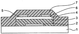
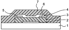
- FIG. 1 is a schematic cross-sectional view showing the structure of a bottom gate top contact organic thin film transistor according to an embodiment of the present invention.
- the organic thin film transistor includes a substrate 1, a gate electrode 2 formed on the substrate 1, a gate insulating layer 3 formed on the gate electrode 2, an organic semiconductor layer 4 formed on the gate insulating layer 3, A source electrode 5 and a drain electrode 6 formed on the organic semiconductor layer 4 with a channel portion interposed therebetween, and an overcoat 7 covering the entire element are provided.
- a bottom gate top contact type organic thin film transistor includes, for example, a gate electrode formed on a substrate, a gate insulating layer formed on the gate electrode, an organic semiconductor layer formed on the gate insulating layer, and a source electrode formed on the organic semiconductor layer. It can be manufactured by forming a drain electrode and forming an overcoat.
- the organic thin film transistor insulating layer material of the present invention is suitably used for forming a gate insulating layer as an organic thin film transistor gate insulating layer material. Moreover, it can also be used for forming an overcoat layer as an organic thin film transistor overcoat layer material.
- FIG. 2 is a schematic cross-sectional view showing the structure of a bottom gate bottom contact type organic thin film transistor which is an embodiment of the present invention.
- a substrate 1 a gate electrode 2 formed on the substrate 1, a gate insulating layer 3 formed on the gate electrode 2, and a channel portion on the gate insulating layer 3 are formed.
- a bottom gate bottom contact type organic thin film transistor includes, for example, a gate electrode formed on a substrate, a gate insulating layer formed on the gate electrode, a source electrode and a drain electrode formed on the gate insulating layer, and a source electrode and a drain electrode. It can be manufactured by forming an organic semiconductor layer thereon and forming an overcoat.
- the organic thin film transistor insulating layer material of the present invention is suitably used for forming a gate insulating layer as an organic thin film transistor gate insulating layer material. Moreover, it can also be used for forming an overcoat layer as an organic thin film transistor overcoat layer material.
- the “base material” refers to a constituent member of the organic thin film transistor on which the organic thin film transistor insulating layer is disposed.
- the organic solvent used in the insulating layer coating solution is not particularly limited as long as it dissolves the organic thin film transistor insulating layer material, but is preferably an organic solvent having a boiling point of 100 ° C. to 200 ° C. at normal pressure. .
- organic solvent examples include 2-heptanone (boiling point 151 ° C.) and propylene glycol monomethyl ether acetate (boiling point 146 ° C.).
- a leveling agent, a surfactant, a curing catalyst, and the like can be added to the insulating layer coating solution as necessary.
- the insulating layer coating solution can be applied onto the organic semiconductor compound or the gate electrode by a known method such as spin coating, die coating, screen printing, or inkjet.
- the formed coating layer is dried as necessary. Drying here means removing the solvent contained in the applied resin composition.
- the dried coating layer is then cured.
- Curing means that the organic thin film transistor insulating layer material is crosslinked.
- Crosslinking of the transistor insulating layer material is performed, for example, by irradiating the coating layer with electromagnetic waves or electron beams.
- the organic thin film transistor insulating layer material contains a catalyst that promotes crosslinking such as a cationic photopolymerization initiator, the catalyst that promotes crosslinking decomposes upon irradiation with electromagnetic waves or electron beams to generate an acid, and the polymer compound (A)
- the cyclic ether in the ring opens to polymerize the polymer compound (A).
- the acid removes a group that can be eliminated by the acid in the repeating unit represented by the formula (1) to form a phenolic hydroxyl group, and the phenolic hydroxyl group and the cyclic ether are ring-opened.
- the growth terminal of the polymer obtained by polymerizing the molecular compound (A) reacts.
- One embodiment of the method for forming an organic thin film transistor insulating layer of the present invention includes a step of applying a liquid containing an organic thin film transistor insulating layer material to a base material to form a coating layer on the base material; Irradiating with a line.
- the polymer compound (A) has a first functional group, and the first functional group is a functional group capable of generating a second functional group capable of reacting with active hydrogen upon irradiation with electromagnetic waves, It is preferable to form an organic thin film transistor insulating layer by the forming method.
- Another aspect of the method for forming an organic thin film transistor insulating layer of the present invention includes a step of applying a liquid containing an organic thin film transistor insulating layer material to a base material to form a coating layer on the base material; Irradiating with an electron beam.
- the organic thin film transistor insulating layer is formed by the forming method, and the organic thin film transistor insulating layer is formed by applying a liquid containing an organic thin film transistor insulating layer material to a base material to form a coating layer on the base material; More preferably, the layer is formed by a forming method including a step of irradiating the layer with electromagnetic waves or an electron beam; and a step of applying heat to the coating layer.
- the coating layer When heat is applied to the coating layer, the coating layer is heated to a temperature of about 80 to 250 ° C., preferably about 100 to 230 ° C., and maintained for about 5 to 120 minutes, preferably about 10 to 60 minutes. If the heating temperature is too low or the heating time is too short, the insulating layer is not sufficiently crosslinked, and if the heating temperature is too high or the heating time is too long, the insulating layer may be damaged.
- the irradiation conditions are adjusted in consideration of the degree of crosslinking and damage of the insulating layer.
- the application condition is adjusted in consideration of the cross-linking of the insulating layer and the degree of damage.
- the wavelength of the electromagnetic wave to be irradiated is preferably 450 nm or less, more preferably 150 to 410 nm.
- the organic thin film transistor insulating layer material may be insufficiently crosslinked.
- electromagnetic waves ultraviolet rays are preferable.
- Irradiation with ultraviolet rays can be performed using, for example, an exposure apparatus used for manufacturing a semiconductor or a UV lamp used for curing a UV curable resin.
- the electron beam irradiation can be performed using, for example, a micro electron beam irradiation tube. Heating can be performed using a heater, an oven, or the like.
- a self-assembled monolayer may be formed on the gate insulating layer.
- the self-assembled monolayer can be formed, for example, by treating the gate insulating layer with a solution obtained by dissolving 1 to 10% by weight of an alkylchlorosilane compound or an alkylalkoxysilane compound in an organic solvent.
- alkylchlorosilane compound examples include methyltrichlorosilane, ethyltrichlorosilane, butyltrichlorosilane, decyltrichlorosilane, and octadecyltrichlorosilane.
- alkylalkoxysilane compound examples include methyltrimethoxysilane, ethyltrimethoxysilane, butyltrimethoxysilane, decyltrimethoxysilane, and octadecyltrimethoxysilane.
- the substrate 1, gate electrode 2, source electrode 5, drain electrode 6 and organic semiconductor layer 4 may be composed of commonly used materials and methods. Resin or plastic plates, films, glass plates, silicon plates, etc. are used as the material of the substrate. As the electrode material, chromium, gold, silver, aluminum, molybdenum, or the like is used, and the electrode is formed by a known method such as a vapor deposition method, a sputtering method, a printing method, or an ink jet method.
- a ⁇ -conjugated polymer is used as the organic semiconductor compound for forming the organic semiconductor layer 4.
- polypyrroles, polythiophenes, polyanilines, polyallylamines, fluorenes, polycarbazoles, polyindoles, poly (P -Phenylene vinylene) and the like can be used.
- low-molecular substances having solubility in organic solvents for example, polycyclic aromatic derivatives such as pentacene, phthalocyanine derivatives, perylene derivatives, tetrathiafulvalene derivatives, tetracyanoquinodimethane derivatives, fullerenes, carbon nanotubes Etc. can be used.
- the organic semiconductor layer can be formed, for example, by adding a solvent or the like if necessary for the organic semiconductor compound, preparing an organic semiconductor coating solution, applying the organic semiconductor coating solution on the gate insulating layer, and applying the organic semiconductor coating solution to the organic semiconductor coating solution. This is done by drying.
- the resin constituting the gate insulating layer has a benzene ring and has an affinity for an organic semiconductor compound. Therefore, a uniform and flat interface is formed between the organic semiconductor layer and the gate insulating layer by the coating and drying method.
- the solvent used in the organic semiconductor coating solution is not particularly limited as long as it dissolves or disperses the organic semiconductor, but is preferably a solvent having a boiling point of 50 ° C. to 200 ° C. at normal pressure.
- the solvent include chloroform, toluene, anisole, 2-heptanone, and propylene glycol monomethyl ether acetate.
- the organic semiconductor coating liquid can be applied onto the gate insulating layer by a known method such as spin coating, die coating, screen printing, and ink jet, in the same manner as the insulating layer coating liquid.
- the organic thin film transistor of the present invention may be coated with an overcoat material for the purpose of protecting the organic thin film transistor and improving the smoothness of the surface.
- the insulating layer manufactured using the organic thin film transistor insulating layer material of the present invention can be laminated with a flat film or the like, and a laminated structure can be easily formed. Moreover, an organic electroluminescent element can be suitably mounted on the insulating layer.
- a display member having an organic thin film transistor can be suitably produced using the organic thin film transistor insulating layer material of the present invention.
- a display provided with a display member can be manufactured using the display member having the organic thin film transistor.
- the organic thin film transistor insulating layer material of the present invention can also be used for forming a layer included in a transistor other than an insulating layer and a layer included in an organic electroluminescence element.
- Synthesis example 1 (Synthesis of polymer compound 1) In a 50 ml pressure vessel (Ace), 5.63 g of 4- (1-ethoxyethoxy) styrene (Tosoh Organic Chemical), 2.50 g of glycidyl methacrylate (Wako Pure Chemical Industries), 2- (O- [1 ′ -Methylpropylideneamino] carboxyamino) ethyl methacrylate (made by Showa Denko, trade name “Karenz MOI-BM”) 2.81 g, 0.05 g of 2,2′-azobis (2-methylpropionitrile), 16.49 g of 2-heptanone (manufactured by Tokyo Chemical Industry Co., Ltd.) was added, and after argon gas was bubbled, it was sealed.
- the high molecular compound 1 has the following repeating unit.
- the numbers in parentheses indicate the mole fraction of repeating units.
- Synthesis example 2 (Synthesis of Compound 2-A) A 300 ml three-necked flask equipped with a three-way cock and septum was charged with 33.29 g of 3-ethyl-3-hydroxymethyloxetane (manufactured by Toagosei Co., Ltd., trade name: OXT-101) and 48 of triethylamine (manufactured by Wako Pure Chemical Industries). .31 g, 200 ml of dehydrated tetrahydrofuran (manufactured by Wako Pure Chemical Industries, Ltd.) and a stir bar were added, and the air inside the flask was replaced with nitrogen.
- the flask was immersed in an ice bath, and 25.00 g of methacryloyl chloride was slowly added dropwise using a gas tight syringe while stirring the reaction mixture by stirring the stirring bar with a magnetic stirrer. After completion of the dropwise addition, the mixture was further stirred for 2 hours in an ice bath, and then stirred overnight at room temperature for reaction. After completion of the reaction, the produced triethylamine hydrochloride was filtered off, the filtrate was transferred to a 500 ml separatory funnel, 200 ml of diethyl ether was added to the filtrate, the organic layer was washed with 100 ml of ion-exchanged water, and the organic layer was separated. Liquid.
- Synthesis example 3 (Synthesis of polymer compound 2) In a 50 ml pressure vessel (manufactured by ACE), 3.00 g of compound 2-A, 4.80 g of 4- (1-ethoxyethoxy) styrene (manufactured by Tosoh Organic Chemical), 2- (O- [1′-methylpropylidene) Amino] carboxyamino) ethyl methacrylate (made by Showa Denko, trade name “Karenz MOI-BM”) 2.40 g, 2,2′-azobis (2-methylpropionitrile) 0.05 g, 2-heptanone ( 15.38 g (manufactured by Tokyo Chemical Industry Co., Ltd.) was added, and after argon gas was bubbled, it was sealed.
- the high molecular compound 2 has the following repeating unit.
- the numbers in parentheses indicate the mole fraction of repeating units.
- Synthesis example 4 (Synthesis of polymer compound 3) In a 50 ml pressure vessel (Ace), 3.38 g of 4- (1-ethoxyethoxy) styrene (Tosoh Organic Chemical), 2.50 g of glycidyl methacrylate (Wako Pure Chemical), and acrylonitrile (Wako Pure Chemical) 0.62 g, 2- (O- [1′-methylpropylideneamino] carboxyamino) ethyl-methacrylate (manufactured by Showa Denko, trade name “Karenz MOI-BM”) 2.81 g, 2,2′-azobis ( 0.05 g of 2-methylpropionitrile) and 14.04 g of 2-heptanone (manufactured by Tokyo Chemical Industry Co., Ltd.) were added, and after argon gas was bubbled, it was sealed.
- the high molecular compound 3 has the following repeating unit.
- the numbers in parentheses indicate the mole fraction of repeating units.
- Synthesis example 5 (Synthesis of polymer compound 4) 1.88 g of 2,1,3-benzothiadiazole-4,7-di (ethylene boronate) and 2,6-dibromo- (4,4-bis-hexadecanyl-4H-cyclopenta [2,1-b; 0.75 g of tetrakis (triphenylphosphine) palladium, methyltrioctylammonium chloride (made by Aldrich, trade name) in 80 mL of toluene 80 containing 3.81 g of 3,4-b ′]-dithiophene) under nitrogen atmosphere 1.0 g of “Aliquat 336” (registered trademark)) and 24 mL of 2M aqueous sodium carbonate solution were added.
- the resulting mixture was stirred vigorously and heated to reflux for 24 hours.
- the viscous reaction mixture was poured into 500 mL of acetone to precipitate a fibrous yellow polymer.
- the polymer was collected by filtration, washed with acetone, and dried in a vacuum oven at 60 ° C. overnight.
- the resulting polymer is referred to as polymer compound 4.
- the high molecular compound 4 has the following repeating unit. n indicates the number of repeating units.
- Synthesis Example 6 (Synthesis of polymer compound 5) In a 50 ml pressure vessel (manufactured by Ace), 1.92 g of 4- (1-ethoxyethoxy) styrene (manufactured by Tosoh Organic Chemical), 4.00 g of compound 2-A, 0.71 g of acrylonitrile (manufactured by Wako Pure Chemical Industries), 1.60 g of 2- (O- [1′-methylpropylideneamino] carboxyamino) ethyl methacrylate (made by Showa Denko, trade name “Karenz MOI-BM”) and 1.74 g of styrene (made by Wako Pure Chemical Industries, Ltd.) Then, 0.05 g of 2,2′-azobis (2-methylpropionitrile) and 23.36 g of 2-heptanone (manufactured by Tokyo Chemical Industry Co., Ltd.) were added, and after argon gas was bubbled, it was sealed.
- the high molecular compound 5 has the following repeating unit.
- the numbers in parentheses indicate the mole fraction of repeating units.
- Synthesis example 7 (Synthesis of polymer compound 6) 1. 50 g of 4- (1-ethoxyethoxy) styrene (manufactured by Tosoh Organic Chemical), 3.00 g of compound 2-A, and 0.46 g of glycidyl methacrylate (manufactured by Wako Pure Chemical Industries) in a 50 ml pressure vessel (made by Ace) , 4.19 g of 4-vinylanisole (Aldrich), 0.69 g of acrylonitrile (manufactured by Wako Pure Chemical Industries), 2- (O- [1′-methylpropylideneamino] carboxyamino) ethyl-methacrylate (manufactured by Showa Denko) , 0.78 g of trade name “Karenz MOI-BM”), 0.33 g of methyl methacrylate (manufactured by Wako Pure Chemical Industries), 0.04 g of 2,2′-azobis (2-methylpropionitrile
- the high molecular compound 5 has the following repeating unit.
- the numbers in parentheses indicate the mole fraction of repeating units.
- Synthesis Example 8 (Synthesis of polymer compound 7) 1. 50 g of 4- (1-ethoxyethoxy) styrene (manufactured by Tosoh Organic Chemical), 3.00 g of compound 2-A, and 0.46 g of glycidyl methacrylate (manufactured by Wako Pure Chemical Industries) in a 50 ml pressure vessel (made by Ace) , 2.19 g of 4-vinylanisole (Aldrich), 0.69 g of acrylonitrile (Wako Pure Chemical), 0.65 g of methyl methacrylate (Wako Pure Chemical), 2,2′-azobis (2-methylpro 0.04 g of (pionitrile) and 20.79 g of 2-heptanone (manufactured by Tokyo Chemical Industry Co., Ltd.) were added, and after argon gas was bubbled, it was sealed.
- Polymerization was carried out in an oil bath at 80 ° C. for 8 hours to obtain a viscous 2-heptanone solution in which the polymer compound 7 was dissolved.
- the polymer compound 7 has the following repeating unit.
- the numbers in parentheses indicate the mole fraction of repeating units.
- Synthesis Example 9 (Synthesis of Compound 8-A) In a 500 ml three-necked flask equipped with a Dimroth, 10.00 g of vinylbenzyl chloride (manufactured by Aldrich), 17.69 g of N, N-diethyldithiocarbamate trihydrate (manufactured by Wako Pure Chemical Industries), acetone (Japanese 200 ml of Koyo Pure Chemical Co., Ltd.) and a stirrer were placed, the flask was immersed in an oil bath, and the mixture was allowed to react for 20 hours while stirring the stirrer with a magnetic stirrer under reflux.
- Synthesis Example 10 (Synthesis of polymer compound 8) In a 50 ml pressure vessel (Ace), 1.88 g of 4- (1-ethoxyethoxy) styrene (Tosoh Organic Chemical), 3.00 g of Compound 2-A, 0.69 g of acrylonitrile (Wako Pure Chemical Industries), 0.86 g of compound 8-A, 0.33 g of methyl methacrylate (manufactured by Wako Pure Chemical Industries), 0.46 g of glycidyl methacrylate (manufactured by Wako Pure Chemical Industries), 2.19 g of 4-vinylanisole (manufactured by Aldrich), 0.05 g of 2′-azobis (2-methylpropionitrile) and 22.05 g of 2-heptanone (manufactured by Tokyo Chemical Industry Co., Ltd.) were added, and after argon gas was bubbled, it was sealed.
- Polymerization was performed in an oil bath at 80 ° C. for 8 hours to obtain a viscous 2-heptanone solution in which the polymer compound 8 was dissolved.
- the polymer compound 8 has the following repeating unit.
- the numbers in parentheses indicate the mole fraction of repeating units.
- Synthesis Example 11 (Synthesis of polymer compound 9) In a 50 ml pressure vessel (Ace), 1.73 g of 4- (1-ethoxyethoxy) styrene (Tosoh Organic Chemical), 3.00 g of Compound 2-A, 0.43 g of glycidyl methacrylate (Wako Pure Chemical) , 2.01 g of 4-vinylanisole (manufactured by Aldrich), 0.64 g of acrylonitrile (manufactured by Wako Pure Chemical Industries), 2- (O- [1′-methylpropylideneamino] carboxyamino) ethyl-methacrylate (manufactured by Showa Denko) , 1.44 g of trade name “Karenz MOI-BM”), 0.05 g of 2,2′-azobis (2-methylpropionitrile), 21.68 g of 2-heptanone (manufactured by Tokyo Chemical Industry), and argon gas was bubbled and sealed.
- the high molecular compound 9 has the following repeating unit.
- the numbers in parentheses indicate the mole fraction of repeating units.
- Example 1 (Production of organic thin film transistor insulating layer material and field effect organic thin film transistor)
- 2-heptanone solution of polymer compound 1 obtained in Synthesis Example 1 and 0.004 g of photoinitiator PI-2074 (manufactured by Rhodia), a photocationic polymerization initiator, are added.
- photoinitiator PI-2074 manufactured by Rhodia
- PI-2074 photoinitiator
- 2-heptanone a photocationic polymerization initiator
- the obtained coating solution 1 was filtered using a membrane filter having a pore diameter of 0.2 ⁇ m, spin-coated on a glass substrate with a chromium electrode, and then dried on a hot plate at 100 ° C. for 1 minute. Thereafter, UV light (wavelength 365 nm) of 600 mJ / cm 2 was irradiated using an aligner (manufactured by Canon; PLA-521), and then fired in nitrogen on a hot plate at 220 ° C. for 30 minutes to obtain a gate insulating layer. It was.
- the polymer compound 4 was dissolved in xylene as a solvent to prepare a solution (organic semiconductor composition) having a concentration of 0.5% by weight, and the solution was filtered through a membrane filter to prepare a coating solution. .
- the obtained coating solution is applied on the gate insulating layer by a spin coating method to form an active layer having a thickness of about 30 nm, and then, on the active layer by a vacuum deposition method using a metal mask,
- a field effect organic thin film transistor was manufactured by forming a source electrode and a drain electrode having a channel length of 20 ⁇ m and a channel width of 2 mm.
- the source electrode and the drain electrode have a structure in which molybdenum oxide and gold are stacked from the active layer side.
- the field effect organic thin film transistor thus fabricated has the transistor characteristics of a vacuum probe (BCT22MDC-5-5) under the condition that the gate voltage Vg is changed to 20 to -40V and the source-drain voltage Vsd is changed to 0 to -40V.
- HT-SCU manufactured by Nagase Electronic Equipments Service Co., LTD. The results are shown in Table 1.
- the hysteresis of the field effect organic thin film transistor is that the source-drain voltage Vsd is ⁇ 40 V, and the threshold voltage Vth1 and the gate voltage Vg are changed from ⁇ 40 V to 20 V when the gate voltage Vg is changed from 20 V to ⁇ 40 V. It was expressed as a voltage difference from the threshold voltage Vth2.
- Example 2 (Production of organic thin film transistor insulating layer material and field effect organic thin film transistor)
- a 10 ml sample bottle 1.00 g of the 2-heptanone solution of the polymer compound 2 obtained in Synthesis Example 3, 0.004 g of photoinitiator PI-2074 (manufactured by Rhodia), and 0.004 g of DBA (manufactured by Kawasaki Kasei).
- 0008 g and 2.00 g of 2-heptanone were added and dissolved while stirring to prepare a uniform coating solution 2 as an organic thin film transistor insulating layer material.
- a field effect organic thin film transistor was prepared in the same manner as in Example 1 except that the coating solution 2 was used instead of the coating solution 1, and the transistor characteristics were evaluated. The results are shown in Table 1.
- Example 3 (Production of organic thin film transistor insulating layer material and field effect organic thin film transistor)
- 2-heptanone solution of polymer compound 3 obtained in Synthesis Example 4 0.004 g of photoinitiator PI-2074 (manufactured by Rhodia), and 0.004 g of DBA (manufactured by Kawasaki Kasei).
- PI-2074 photoinitiator
- DBA manufactured by Kawasaki Kasei
- 0008 g and 2.00 g of 2-heptanone were added and dissolved while stirring to prepare a uniform coating solution 3 as an organic thin film transistor insulating layer material.
- a field effect organic thin film transistor was prepared in the same manner as in Example 1 except that the coating solution 3 was used instead of the coating solution 1, and the transistor characteristics were evaluated. The results are shown in Table 1.
- Example 4 (Production of organic thin film transistor insulating layer material and field effect organic thin film transistor)
- a 10 ml sample bottle 1.00 g of the 2-heptanone solution of the polymer compound 5 obtained in Synthesis Example 6, 0.004 g of photoinitiator PI-2074 (manufactured by Rhodia), and 0.004 g of DBA (manufactured by Kawasaki Kasei).
- 0008 g and 2.00 g of 2-heptanone were added and dissolved while stirring to prepare a uniform coating solution 4 as an organic thin film transistor insulating layer material.
- a field effect organic thin film transistor was prepared in the same manner as in Example 1 except that the coating solution 4 was used instead of the coating solution 1, and the transistor characteristics were evaluated. The results are shown in Table 1.
- Example 5 (Production of organic thin film transistor insulating layer material and field effect organic thin film transistor)
- a 10 ml sample bottle 1.00 g of the 2-heptanone solution of the polymer compound 6 obtained in Synthesis Example 7, 0.004 g of photoinitiator PI-2074 (manufactured by Rhodia), and 0.004 g of DBA (manufactured by Kawasaki Kasei).
- 0008 g and 2.00 g of 2-heptanone were added and dissolved while stirring to prepare a uniform coating solution 5 as an organic thin film transistor insulating layer material.
- a field effect organic thin film transistor was prepared in the same manner as in Example 1 except that the coating solution 5 was used instead of the coating solution 1, and the transistor characteristics were evaluated. The results are shown in Table 1.
- Example 6 (Production of organic thin film transistor insulating layer material and field effect organic thin film transistor)
- a 10 ml sample bottle 1.00 g of the 2-heptanone solution of the polymer compound 7 obtained in Synthesis Example 8, 0.004 g of photoinitiator PI-2074 (manufactured by Rhodia), and 0.004 g of DBA (manufactured by Kawasaki Kasei).
- 0008 g and 2.00 g of 2-heptanone were added and dissolved while stirring to prepare a uniform coating solution 6 as an organic thin film transistor insulating layer material.
- a field effect organic thin film transistor was prepared in the same manner as in Example 1 except that the coating solution 6 was used instead of the coating solution 1, and the transistor characteristics were evaluated. The results are shown in Table 1.
- Example 7 (Production of organic thin film transistor insulating layer material and field effect organic thin film transistor)
- a 2-heptanone solution of polymer compound 8 obtained in Synthesis Example 10 0.015 g of divinylbenzene, 0.004 g of photoinitiator PI-2074 (manufactured by Rhodia), DBA ( Kawasaki Chemical Co., Ltd.) (0.0008 g) and 2-heptanone (1.00 g) were added and dissolved while stirring to prepare a uniform coating solution 7 as an organic thin film transistor insulating layer material.
- a field effect organic thin film transistor was prepared in the same manner as in Example 1 except that the coating solution 7 was used instead of the coating solution 1, and the transistor characteristics were evaluated. The results are shown in Table 1.
- Example 8 (Production of organic thin film transistor insulating layer material and field effect organic thin film transistor)
- a 10 ml sample bottle 1.00 g of the 2-heptanone solution of polymer compound 2 obtained in Synthesis Example 3, 0.008 g of photoacid generator LW-S1 (manufactured by San Apro), and 1.00 g of 2-heptanone are placed. Then, the mixture was dissolved with stirring to prepare a uniform coating solution 8 as an organic thin film transistor insulating layer material.
- a field effect organic thin film transistor was prepared in the same manner as in Example 1 except that the coating solution 8 was used instead of the coating solution 1, and the transistor characteristics were evaluated. The results are shown in Table 1.
- Example 9 (Production of organic thin film transistor insulating layer material and field effect organic thin film transistor)
- a 10 ml sample bottle add 1.50 g of the 2-heptanone solution of the polymer compound 9 obtained in Synthesis Example 11, 0.009 g of the photoacid generator LW-S1 (manufactured by San Apro), and 1.00 g of 2-heptanone.
- the mixture was dissolved with stirring to prepare a uniform coating solution 9 as an organic thin film transistor insulating layer material.
- a field effect organic thin film transistor was prepared in the same manner as in Example 1 except that the coating solution 9 was used instead of the coating solution 1, and the transistor characteristics were evaluated. The results are shown in Table 1.
- Comparative Example 1 Manufacture of field-effect organic thin-film transistors
- a field effect organic thin film transistor was produced in the same manner as in Example 1 except that the coating solution 8 was used in place of the coating solution 1 and UV irradiation was not performed when forming the gate insulating layer. When the transistor characteristics were measured and evaluated, it did not operate as a transistor in the region where the gate voltage Vg was 20V to -40V.
Landscapes
- Chemical & Material Sciences (AREA)
- Health & Medical Sciences (AREA)
- Organic Chemistry (AREA)
- Polymers & Plastics (AREA)
- Chemical Kinetics & Catalysis (AREA)
- Medicinal Chemistry (AREA)
- Engineering & Computer Science (AREA)
- Materials Engineering (AREA)
- Emergency Medicine (AREA)
- Physics & Mathematics (AREA)
- Spectroscopy & Molecular Physics (AREA)
- Wood Science & Technology (AREA)
- Life Sciences & Earth Sciences (AREA)
- Geometry (AREA)
- Microelectronics & Electronic Packaging (AREA)
- Thin Film Transistor (AREA)
- Addition Polymer Or Copolymer, Post-Treatments, Or Chemical Modifications (AREA)
- Formation Of Insulating Films (AREA)
- Electroluminescent Light Sources (AREA)
Abstract
Description
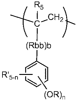
で表される繰り返し単位とを含有する高分子化合物(A)を含む有機薄膜トランジスタ絶縁層材料を提供する。

で表される繰り返し単位、及び、式(3)
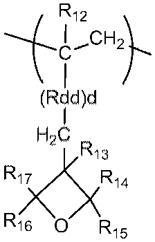
で表される繰り返し単位、からなる群より選ばれる少なくとも1種の繰り返し単位である。

で表される基である。

で表される基である。
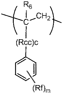
で表される繰り返し単位を含有する。
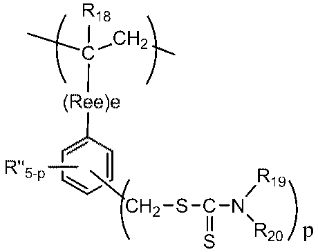
で表される繰り返し単位を含有する。
該塗布層に電磁波又は電子線を照射する工程;
を包含する有機薄膜トランジスタ絶縁層の形成方法を提供する。
該塗布層に電磁波又は電子線を照射する工程;及び
該塗布層に熱を印加する工程;
を包含する有機薄膜トランジスタ絶縁層の形成方法を提供する。
Reeで表される炭素数1~20の二価の有機基の具体例としては、前述のRbbで表される炭素数1~20の二価の有機基の具体例と同じ基が挙げられる。
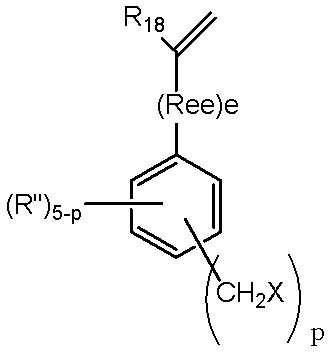
で表される構造の重合性モノマーを使用すること以外は前記と同様にしてモノマー混合物の共重合を行い、次いで、N,N-ジアルキルチオカルバミック酸金属塩と反応させる方法により製造してもよい。
(メトキシエトキシメトキシ)スチレン-コ-3-メタクリロイルオキシメチル-3-エチルオキセタン-コ-3-(N,N-ジエチルジチオカルバミルメチル)スチレン)が挙げられる。
本発明の有機薄膜トランジスタ絶縁層材料は、混合や粘度調節のための溶媒や、高分子化合物(A)を架橋させるために用いる架橋剤、該架橋剤と組み合わせて用いられる添加剤などを含有していてもよい。該溶媒としては、テトラヒドロフランやジエチルエーテルなどのエーテル溶媒、ヘキサンなどの脂肪族炭化水素溶媒、シクロヘキサンなどの脂環式炭化水素溶媒、ペンテン等の不飽和炭化水素溶媒、キシレンなどの芳香族炭化水素溶媒、アセトンなどのケトン溶媒、ブチルアセテートなどのアセテート溶媒、イソプロピルアルコールなどのアルコール溶媒、クロロホルムなどのハロゲン溶媒、これらの溶媒の混合溶媒が挙げられる。また、添加剤としては、架橋反応を促進するための触媒、増感剤、レべリング剤、粘度調節剤などを用いることができる。
図1は、本発明の一実施形態であるボトムゲートトップコンタクト型有機薄膜トランジスタの構造を示す模式断面図である。この有機薄膜トランジスタには、基板1と、基板1上に形成されたゲート電極2と、ゲート電極2上に形成されたゲート絶縁層3と、ゲート絶縁層3上に形成された有機半導体層4と、有機半導体層4上にチャネル部を挟んで形成されたソース電極5及びドレイン電極6と、素子全体を覆うオーバーコート7とが、備えられている。
(高分子化合物1の合成)
50ml耐圧容器(エース製)に、4-(1-エトキシエトキシ)スチレン(東ソー有機化学製)を5.63g、グリシジルメタクリレート(和光純薬製)を2.50g、2-(O-[1’-メチルプロピリデンアミノ]カルボキシアミノ)エチル-メタクリレート(昭和電工製、商品名「カレンズMOI-BM」)を2.81g、2,2’-アゾビス(2-メチルプロピオニトリル)を0.05g、2-ヘプタノン(東京化成製)を16.49g入れ、アルゴンガスをバブリングした後、密栓した。60℃のオイルバス中で20時間重合させ、高分子化合物1が溶解している粘稠な2-ヘプタノン溶液を得た。高分子化合物1は、下記繰り返し単位を有している。括弧の添え数字は繰り返し単位のモル分率を示している。
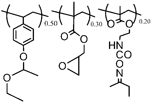
(化合物2-Aの合成)
三方コック及びセプタムを取り付けた300mlの三つ口フラスコに、3-エチル-3-ヒドロキシメチルオキセタン(東亞合成製、商品名:OXT-101)を33.29g、トリエチルアミン(和光純薬製)を48.31g、脱水テトラヒドロフラン(和光純薬製)を200ml、攪拌子を入れ、フラスコ内部の空気を窒素で置換した。フラスコを氷浴中に浸け、マグネティックスターラーで攪拌子を攪拌させることにより反応混合物を攪拌させながら、ガスタイトシリンジを用いてメタクリロイルクロライド25.00gをゆっくり滴下した。滴下終了後、氷浴中で更に2時間攪拌を続け、その後、室温で一晩攪拌を続けて反応させた。反応終了後、生成したトリエチルアミン塩酸塩を濾別し、濾液を500mlの分液ロートに移し、濾液にジエチルエーテル200mlを加えた後、100mlのイオン交換水で有機層を水洗し、有機層を分液した。有機層の水洗を3回繰り返した後、有機層を分液し、無水硫酸マグネシウムを加えて乾燥させた。無水硫酸マグネシウムを濾別した後、濾液をロータリーエバポレーターを用いて濃縮し、化合物2-Aを淡褐色液体として得た。化合物2-Aの得量は29.3gであり、収率は61.3%であった。
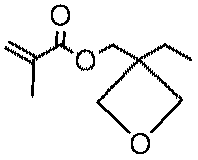
(高分子化合物2の合成)
50ml耐圧容器(エース製)に、化合物2-Aを3.00g、4-(1-エトキシエトキシ)スチレン(東ソー有機化学製)を4.80g、2-(O-[1’-メチルプロピリデンアミノ]カルボキシアミノ)エチル-メタクリレート(昭和電工製、商品名「カレンズMOI-BM」)を2.40g、2,2’-アゾビス(2-メチルプロピオニトリル)を0.05g、2-ヘプタノン(東京化成製)を15.38g入れ、アルゴンガスをバブリングした後、密栓した。60℃のオイルバス中で20時間重合させ、高分子化合物2が溶解している粘稠な2-ヘプタノン溶液を得た。高分子化合物2は、下記繰り返し単位を有している。括弧の添え数字は繰り返し単位のモル分率を示している。

(高分子化合物3の合成)
50ml耐圧容器(エース製)に、4-(1-エトキシエトキシ)スチレン(東ソー有機化学製)を3.38g、グリシジルメタクリレート(和光純薬製)を2.50g、アクリロニトリル(和光純薬製)を0.62g、2-(O-[1’-メチルプロピリデンアミノ]カルボキシアミノ)エチル-メタクリレート(昭和電工製、商品名「カレンズMOI-BM」)を2.81g、2,2’-アゾビス(2-メチルプロピオニトリル)を0.05g、2-ヘプタノン(東京化成製)を14.04g入れ、アルゴンガスをバブリングした後、密栓した。60℃のオイルバス中で20時間重合させ、高分子化合物3が溶解している粘稠な2-ヘプタノン溶液を得た。高分子化合物3は、下記繰り返し単位を有している。括弧の添え数字は繰り返し単位のモル分率を示している。
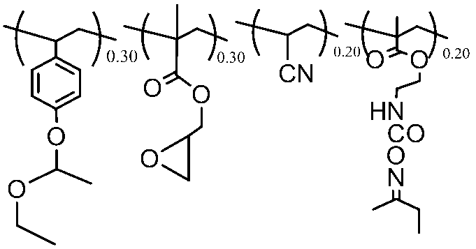
(高分子化合物4の合成)
2,1,3-ベンゾチアジアゾール-4,7-ジ(エチレンボロネート)を1.88g、及び2,6-ジブロモ-(4,4-ビス-ヘキサデカニル-4H-シクロペンタ[2,1-b;3,4-b’]-ジチオフェン)を3.81g含む80mLのトルエン80中に、窒素雰囲気下において、テトラキス(トリフェニルホスフィン)パラジウムを0.75g、メチルトリオクチルアンモニウムクロライド(Aldrich製、商品名「Aliquat 336」(登録商標))を1.0g、及び2Mの炭酸ナトリウム水溶液を24mL加えた。得られた混合物を激しく攪拌し、加熱して24時間還流させた。粘稠な反応混合物をアセトン500mLに注ぎ、繊維状の黄色のポリマーを沈澱させた。このポリマーを濾過して集め、アセトンで洗浄し、真空オーブンにおいて60℃で一晩乾燥させた。得られたポリマーを高分子化合物4とよぶ。高分子化合物4は、下記繰り返し単位を有している。nは繰り返し単位の数を示している。

(高分子化合物5の合成)
50ml耐圧容器(エース製)に、4-(1-エトキシエトキシ)スチレン(東ソー有機化学製)を1.92g、化合物2-Aを4.00g、アクリロニトリル(和光純薬製)を0.71g、2-(O-[1’-メチルプロピリデンアミノ]カルボキシアミノ)エチル-メタクリレート(昭和電工製、商品名「カレンズMOI-BM」)を1.60g、スチレン(和光純薬製)を1.74g、2,2’-アゾビス(2-メチルプロピオニトリル)を0.05g、2-ヘプタノン(東京化成製)を23.36g入れ、アルゴンガスをバブリングした後、密栓した。60℃のオイルバス中で20時間重合させ、高分子化合物5が溶解している粘稠な2-ヘプタノン溶液を得た。高分子化合物5は、下記繰り返し単位を有している。括弧の添え数字は繰り返し単位のモル分率を示している。

(高分子化合物6の合成)
50ml耐圧容器(エース製)に、4-(1-エトキシエトキシ)スチレン(東ソー有機化学製)を1.88g、化合物2-Aを3.00g、グリシジルメタクリレート(和光純薬製)を0.46g、4-ビニルアニソール(アルドリッチ製)を2.19g、アクリロニトリル(和光純薬製)を0.69g、2-(O-[1’-メチルプロピリデンアミノ]カルボキシアミノ)エチル-メタクリレート(昭和電工製、商品名「カレンズMOI-BM」)を0.78g、メチルメタクリレート(和光純薬製)を0.33g、2,2’-アゾビス(2-メチルプロピオニトリル)を0.04g、2-ヘプタノン(東京化成製)を21.86g入れ、アルゴンガスをバブリングした後、密栓した。80℃のオイルバス中で8時間重合させ、高分子化合物6が溶解している粘稠な2-ヘプタノン溶液を得た。高分子化合物5は、下記繰り返し単位を有している。括弧の添え数字は繰り返し単位のモル分率を示している。

(高分子化合物7の合成)
50ml耐圧容器(エース製)に、4-(1-エトキシエトキシ)スチレン(東ソー有機化学製)を1.88g、化合物2-Aを3.00g、グリシジルメタクリレート(和光純薬製)を0.46g、4-ビニルアニソール(アルドリッチ製)を2.19g、アクリロニトリル(和光純薬製)を0.69g、メチルメタクリレート(和光純薬製)を0.65g、2,2’-アゾビス(2-メチルプロピオニトリル)を0.04g、2-ヘプタノン(東京化成製)を20.79g入れ、アルゴンガスをバブリングした後、密栓した。80℃のオイルバス中で8時間重合させ、高分子化合物7が溶解している粘稠な2-ヘプタノン溶液を得た。高分子化合物7は、下記繰り返し単位を有している。括弧の添え数字は繰り返し単位のモル分率を示している。
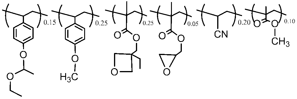
(化合物8-Aの合成)
ジムロートを取り付けた500mlの三つ口フラスコに、ビニルベンジルクロライド(アルドリッチ製)を10.00g、N,N-ジエチルジチオカルバメート・3水和物(和光純薬製)を17.69g、アセトン(和光純薬製)を200ml、及び、攪拌子を入れ、フラスコをオイルバスに漬け、還流下、マグネティックスターラーで攪拌子を攪拌させることにより反応混合物を攪拌させながら、20時間反応させた。反応終了後、析出物を濾別し、濾液をロータリーエバポレーターで濃縮した。得られた粘稠な液体をジエチルエーテル200mlに溶解させた後、100mlのイオン交換水で有機層を水洗し、有機層を分液した。有機層の水洗を3回繰り返した後、有機層を分液し、無水硫酸マグネシウムを加えて乾燥させた。無水硫酸マグネシウムを濾別した後、濾液をロータリーエバポレーターを用いて濃縮し、化合物8-Aを黄褐色液体として得た。化合物8-Aの得量は15gであり、収率は86%であった。
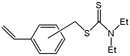
(高分子化合物8の合成)
50ml耐圧容器(エース製)に、4-(1-エトキシエトキシ)スチレン(東ソー有機化学製)を1.88g、化合物2-Aを3.00g、アクリロニトリル(和光純薬製)を0.69g、化合物8-Aを0.86g、メチルメタクリレート(和光純薬製)を0.33g、グリシジルメタクリレート(和光純薬製)を0.46g、4-ビニルアニソール(アルドリッチ製)を2.19g、2,2’-アゾビス(2-メチルプロピオニトリル)を0.05g、2-ヘプタノン(東京化成製)を22.05g入れ、アルゴンガスをバブリングした後、密栓した。80℃のオイルバス中で8時間重合させ、高分子化合物8が溶解している粘稠な2-ヘプタノン溶液を得た。高分子化合物8は、下記繰り返し単位を有している。括弧の添え数字は繰り返し単位のモル分率を示している。
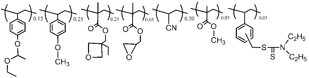
(高分子化合物9の合成)
50ml耐圧容器(エース製)に、4-(1-エトキシエトキシ)スチレン(東ソー有機化学製)を1.73g、化合物2-Aを3.00g、グリシジルメタクリレート(和光純薬製)を0.43g、4-ビニルアニソール(アルドリッチ製)を2.01g、アクリロニトリル(和光純薬製)を0.64g、2-(O-[1’-メチルプロピリデンアミノ]カルボキシアミノ)エチル-メタクリレート(昭和電工製、商品名「カレンズMOI-BM」)を1.44g、2,2’-アゾビス(2-メチルプロピオニトリル)を0.05g、2-ヘプタノン(東京化成製)を21.68g入れ、アルゴンガスをバブリングした後、密栓した。80℃のオイルバス中で8時間重合させ、高分子化合物9が溶解している粘稠な2-ヘプタノン溶液を得た。高分子化合物9は、下記繰り返し単位を有している。括弧の添え数字は繰り返し単位のモル分率を示している。

(有機薄膜トランジスタ絶縁層材料及び電界効果型有機薄膜トランジスタの製造)
10mlのサンプル瓶に、合成例1で得た高分子化合物1の2-ヘプタノン溶液を1.00g、光カチオン重合開始剤であるフォトイニシエーターPI-2074(ローディア製)を0.004g、光増感剤である9,10-ジブトキシアントラセン(DBA)(川崎化成製)を0.0008g、2-ヘプタノンを2.00g入れ、攪拌しながら溶解して、有機薄膜トランジスタ絶縁層材料である均一な塗布溶液1を調製した。
こうして作製した電界効果型有機薄膜トランジスタについて、ゲート電圧Vgを20~-40V、ソース・ドレイン間電圧Vsdを0~-40Vに変化させた条件で、そのトランジスタ特性を真空プロ-バ(BCT22MDC-5-HT-SCU;Nagase Electronic Equipments Service Co., LTD製)を用いて測定した。結果を表1に示す。
(有機薄膜トランジスタ絶縁層材料及び電界効果型有機薄膜トランジスタの製造)
10mlのサンプル瓶に、合成例3で得た高分子化合物2の2-ヘプタノン溶液を1.00g、フォトイニシエーターPI-2074(ローディア製)を0.004g、DBA(川崎化成製)を0.0008g、2-ヘプタノンを2.00g入れ、攪拌しながら溶解して、有機薄膜トランジスタ絶縁層材料である均一な塗布溶液2を調製した。
(有機薄膜トランジスタ絶縁層材料及び電界効果型有機薄膜トランジスタの製造)
10mlのサンプル瓶に、合成例4で得た高分子化合物3の2-ヘプタノン溶液を1.00g、フォトイニシエーターPI-2074(ローディア製)を0.004g、DBA(川崎化成製)を0.0008g、2-ヘプタノンを2.00g入れ、攪拌しながら溶解して、有機薄膜トランジスタ絶縁層材料である均一な塗布溶液3を調製した。
(有機薄膜トランジスタ絶縁層材料及び電界効果型有機薄膜トランジスタの製造)
10mlのサンプル瓶に、合成例6で得た高分子化合物5の2-ヘプタノン溶液を1.00g、フォトイニシエーターPI-2074(ローディア製)を0.004g、DBA(川崎化成製)を0.0008g、2-ヘプタノンを2.00g入れ、攪拌しながら溶解して、有機薄膜トランジスタ絶縁層材料である均一な塗布溶液4を調製した。
(有機薄膜トランジスタ絶縁層材料及び電界効果型有機薄膜トランジスタの製造)
10mlのサンプル瓶に、合成例7で得た高分子化合物6の2-ヘプタノン溶液を1.00g、フォトイニシエーターPI-2074(ローディア製)を0.004g、DBA(川崎化成製)を0.0008g、2-ヘプタノンを2.00g入れ、攪拌しながら溶解して、有機薄膜トランジスタ絶縁層材料である均一な塗布溶液5を調製した。
(有機薄膜トランジスタ絶縁層材料及び電界効果型有機薄膜トランジスタの製造)
10mlのサンプル瓶に、合成例8で得た高分子化合物7の2-ヘプタノン溶液を1.00g、フォトイニシエーターPI-2074(ローディア製)を0.004g、DBA(川崎化成製)を0.0008g、2-ヘプタノンを2.00g入れ、攪拌しながら溶解して、有機薄膜トランジスタ絶縁層材料である均一な塗布溶液6を調製した。
(有機薄膜トランジスタ絶縁層材料及び電界効果型有機薄膜トランジスタの製造)
10mlのサンプル瓶に、合成例10で得た高分子化合物8の2-ヘプタノン溶液を1.00g、ジビニルベンゼンを0.015g、フォトイニシエーターPI-2074(ローディア製)を0.004g、DBA(川崎化成製)を0.0008g、2-ヘプタノンを1.00g入れ、攪拌しながら溶解して、有機薄膜トランジスタ絶縁層材料である均一な塗布溶液7を調製した。
(有機薄膜トランジスタ絶縁層材料及び電界効果型有機薄膜トランジスタの製造)
10mlのサンプル瓶に、合成例3で得た高分子化合物2の2-ヘプタノン溶液を1.00g、光酸発生剤LW-S1(サンアプロ製)を0.008g、2-ヘプタノンを1.00g入れ、攪拌しながら溶解して、有機薄膜トランジスタ絶縁層材料である均一な塗布溶液8を調製した。
(有機薄膜トランジスタ絶縁層材料及び電界効果型有機薄膜トランジスタの製造)
10mlのサンプル瓶に、合成例11で得た高分子化合物9の2-ヘプタノン溶液を1.50g、光酸発生剤LW-S1(サンアプロ製)を0.009g、2-ヘプタノンを1.00g入れ、攪拌しながら溶解して、有機薄膜トランジスタ絶縁層材料である均一な塗布溶液9を調製した。
(電界効果型有機薄膜トランジスタの製造)
10mlのサンプル瓶に、ポリビニルフェノール-コ-ポリメチルメタクリレート(アルドリッチ製、Mn=6700)を1.00g、N,N,N’,N’,N”,N”-ヘキサメトキシメチルメラミン(住友化学製)を0.163g、熱酸発生剤(みどり化学(株)製、商品名:TAZ-108)を0.113g、2-ヘプタノンを7.00g入れ、攪拌溶解して均一な塗布溶液8を調製した。

2…ゲート電極、
3…ゲート絶縁層、
4…有機半導体層、
5…ソース電極、
6…ドレイン電極、
7…オーバーコート。
Claims (15)
- 環状エーテル構造を有する繰り返し単位と、式(1)

[式中、R5は、水素原子又はメチル基を表す。Rbbは、高分子化合物の主鎖と側鎖とを連結し、フッ素原子を有していてもよい連結部分を表す。Rは、酸により脱離しうる有機基を表す。R’は、水素原子又は炭素数1~20の一価の有機基を表す。該炭素数1~20の一価の有機基中の水素原子は、フッ素原子で置換されていてもよい。bは、0又は1の整数を表し、nは、1~5の整数を表す。Rが複数個ある場合、それらは同一であっても相異なってもよい。R’が複数個ある場合、それらは同一であっても相異なってもよい。]
で表される繰り返し単位とを含有する高分子化合物(A)を含む有機薄膜トランジスタ絶縁層材料。 - 前記環状エーテル構造を有する繰り返し単位が、式(2)

[式中、R1は、水素原子又はメチル基を表す。R2~R4は、それぞれ独立に、水素原子又は炭素数1~20の一価の有機基を表す。Raaは、高分子化合物の主鎖と側鎖とを連結し、フッ素原子を有していてもよい連結部分を表す。aは、0又は1の整数を表す。]
で表される繰り返し単位、及び、式(3)

[式中、R12は、水素原子又はメチル基を表す。R13~R17は、それぞれ独立に、水素原子又は炭素数1~20の一価の有機基を表す。Rddは、高分子化合物の主鎖と側鎖とを連結し、フッ素原子を有していてもよい連結部分を表す。dは、0又は1の整数を表す。]
で表される繰り返し単位とからなる群より選ばれる少なくとも1種の繰り返し単位である請求項1に記載の有機薄膜トランジスタ絶縁層材料。 - 前記高分子化合物(A)が、更に、第1の官能基を含有する繰り返し単位であって、該第1の官能基が、活性水素と反応しうる第2の官能基を電磁波もしくは熱の作用により生成しうる官能基である繰り返し単位、を含有する請求項1又は2に記載の有機薄膜トランジスタ絶縁層材料。
- 前記第1の官能基が、ブロック化剤でブロックされたイソシアナト基及びブロック化剤でブロックされたイソチオシアナト基からなる群から選ばれる少なくとも1種の基である請求項3に記載の有機薄膜トランジスタ絶縁層材料。
- 前記ブロック化剤でブロックされたイソシアナト基及びブロック化剤でブロックされたイソチオシアナト基が、式(5)
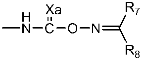
[式中、Xaは、酸素原子又は硫黄原子を表し、R7及びR8は、それぞれ独立に、水素原子又は炭素数1~20の一価の有機基を表す。]
で表される基である請求項4に記載の有機薄膜トランジスタ絶縁層材料。 - ブロック化剤でブロックされたイソシアナト基及びブロック化剤でブロックされたイソチオシアナト基が、式(6)

[式中、Xbは、酸素原子又は硫黄原子を表し、R9~R11は、それぞれ独立に、水素原子又は炭素数1~20の一価の有機基を表す。]
で表される基である請求項4に記載の有機薄膜トランジスタ絶縁層材料。 - 前記高分子化合物(A)が、更に、式(4)
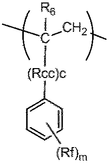
[式中、R6は、水素原子又はメチル基を表す。Rfは、フッ素原子又はフッ素原子を有していてもよい炭素数1~20の一価の有機基を表す。Rccは、高分子化合物の主鎖と側鎖とを連結し、フッ素原子を有していてもよい連結部分を表す。cは、0又は1の整数を表し、mは、1~5の整数を表す。Rfが複数個ある場合、それらは同一でも相異なっていてもよい。ただし、少なくとも1個のRfは、フッ素原子又はフッ素原子を有する炭素数1~20の一価の有機基である。]
で表される繰り返し単位を含有する請求項1~6のいずれか一項に記載の有機薄膜トランジスタ絶縁層材料。 - 前記高分子化合物(A)が、更に、式(8)

[式中、R18は、水素原子又はメチル基を表す。Reeは、高分子化合物の主鎖と側鎖とを連結し、フッ素原子を有していてもよい連結部分を表す。R19、R20及びR’’は、水素原子又は炭素数1~20の一価の有機基を表す。該炭素数1~20の一価の有機基中の水素原子は、フッ素原子で置換されていてもよい。eは、0又は1の整数を表し、pは、1~5の整数を表す。]
で表される繰り返し単位を含有する請求項1~7のいずれか一項に記載の有機薄膜トランジスタ絶縁層材料。 - 請求項1~8のいずれか一項に記載の有機薄膜トランジスタ絶縁層材料を含む液を基材に塗布して該基材上に塗布層を形成する工程;及び
該塗布層に電磁波又は電子線を照射する工程;
を包含する有機薄膜トランジスタ絶縁層の形成方法。 - 請求項1~8のいずれか一項に記載の有機薄膜トランジスタ絶縁層材料を含む液を基材に塗布して該基材上に塗布層を形成する工程;
該塗布層に電磁波又は電子線を照射する工程;及び
該塗布層に熱を印加する工程;
を包含する有機薄膜トランジスタ絶縁層の形成方法。 - 前記電磁波が紫外線である請求項9又は10に記載の有機薄膜トランジスタ絶縁層の形成方法。
- 請求項1~8のいずれか一項に記載の有機薄膜トランジスタ絶縁層材料を用いて形成した有機薄膜トランジスタ絶縁層を有する有機薄膜トランジスタ。
- 前記有機薄膜トランジスタ絶縁層がゲート絶縁層である請求項12に記載の有機薄膜トランジスタ。
- 請求項12又は13に記載の有機薄膜トランジスタを含むディスプレイ用部材。
- 請求項14に記載のディスプレイ用部材を含むディスプレイ。
Priority Applications (2)
| Application Number | Priority Date | Filing Date | Title |
|---|---|---|---|
| US14/118,275 US9035292B2 (en) | 2011-05-24 | 2012-05-22 | Organic thin-film transistor insulating layer material |
| KR1020137033781A KR101888718B1 (ko) | 2011-05-24 | 2012-05-22 | 유기 박막 트랜지스터 절연층 재료 |
Applications Claiming Priority (6)
| Application Number | Priority Date | Filing Date | Title |
|---|---|---|---|
| JP2011-116113 | 2011-05-24 | ||
| JP2011116113 | 2011-05-24 | ||
| JP2011-190914 | 2011-09-01 | ||
| JP2011190914 | 2011-09-01 | ||
| JP2011-228763 | 2011-10-18 | ||
| JP2011228763 | 2011-10-18 |
Publications (1)
| Publication Number | Publication Date |
|---|---|
| WO2012161175A1 true WO2012161175A1 (ja) | 2012-11-29 |
Family
ID=47217251
Family Applications (1)
| Application Number | Title | Priority Date | Filing Date |
|---|---|---|---|
| PCT/JP2012/063002 Ceased WO2012161175A1 (ja) | 2011-05-24 | 2012-05-22 | 有機薄膜トランジスタ絶縁層材料 |
Country Status (5)
| Country | Link |
|---|---|
| US (1) | US9035292B2 (ja) |
| JP (1) | JP6034056B2 (ja) |
| KR (1) | KR101888718B1 (ja) |
| TW (1) | TWI547504B (ja) |
| WO (1) | WO2012161175A1 (ja) |
Cited By (2)
| Publication number | Priority date | Publication date | Assignee | Title |
|---|---|---|---|---|
| JP2014110251A (ja) * | 2012-11-30 | 2014-06-12 | Sumitomo Chemical Co Ltd | 有機薄膜トランジスタ絶縁層材料及び有機薄膜トランジスタ |
| JP2014116530A (ja) * | 2012-12-12 | 2014-06-26 | Sumitomo Chemical Co Ltd | 絶縁層材料及び該絶縁層材料を用いて形成した有機薄膜トランジスタ |
Families Citing this family (11)
| Publication number | Priority date | Publication date | Assignee | Title |
|---|---|---|---|---|
| JP6025326B2 (ja) * | 2011-12-21 | 2016-11-16 | 住友化学株式会社 | 電子デバイス絶縁層材料、及び電子デバイス |
| KR20140131940A (ko) * | 2012-03-01 | 2014-11-14 | 스미또모 가가꾸 가부시키가이샤 | 전자 디바이스 절연층 및 전자 디바이스 절연층의 제조 방법 |
| JP6118287B2 (ja) | 2014-03-26 | 2017-04-19 | 富士フイルム株式会社 | 半導体素子及び半導体素子の絶縁層形成用組成物 |
| JP6204580B2 (ja) | 2014-05-08 | 2017-09-27 | 富士フイルム株式会社 | 薄膜トランジスタ及び絶縁層形成用組成物 |
| CN106688050B (zh) * | 2014-06-11 | 2018-09-18 | 伊斯曼柯达公司 | 具有带含硫代硫酸盐聚合物的电介质层的器件 |
| WO2016194517A1 (ja) * | 2015-05-29 | 2016-12-08 | 富士フイルム株式会社 | 有機薄膜トランジスタ、有機半導体層形成用組成物 |
| JP6632862B2 (ja) * | 2015-10-22 | 2020-01-22 | 株式会社ブリヂストン | 機能性発泡体 |
| US10026911B2 (en) * | 2016-01-15 | 2018-07-17 | Corning Incorporated | Structure for transistor switching speed improvement utilizing polar elastomers |
| WO2017141933A1 (ja) * | 2016-02-18 | 2017-08-24 | 住友化学株式会社 | 高分子化合物、組成物及び有機薄膜トランジスタ |
| CN108172628B (zh) * | 2016-12-07 | 2020-11-06 | 清华大学 | 一种逻辑电路 |
| CN114141708B (zh) * | 2021-11-19 | 2026-03-13 | 惠州华星光电显示有限公司 | 晶体管及其制作方法 |
Citations (4)
| Publication number | Priority date | Publication date | Assignee | Title |
|---|---|---|---|---|
| JP2008040187A (ja) * | 2006-08-07 | 2008-02-21 | Tokyo Ohka Kogyo Co Ltd | 層間絶縁膜の形成方法及び層間絶縁膜用感光性樹脂組成物 |
| JP2009049396A (ja) * | 2007-07-24 | 2009-03-05 | Sumitomo Chemical Co Ltd | 有機トランジスタ絶縁膜用組成物 |
| JP2009102512A (ja) * | 2007-10-23 | 2009-05-14 | Jsr Corp | 絶縁膜形成用感光性樹脂組成物 |
| WO2010024238A1 (ja) * | 2008-08-28 | 2010-03-04 | 住友化学株式会社 | 樹脂組成物、ゲート絶縁層及び有機薄膜トランジスタ |
Family Cites Families (6)
| Publication number | Priority date | Publication date | Assignee | Title |
|---|---|---|---|---|
| JP2000264937A (ja) | 1999-03-15 | 2000-09-26 | Japan Chemical Innovation Institute | ポリ塩化ビニル−ポリスチレンブロック共重合体、ポリ塩化ビニル−ポリ酢酸ビニルブロック共重合体、およびこれらの製造方法 |
| JP4807159B2 (ja) | 2006-04-12 | 2011-11-02 | 凸版印刷株式会社 | 絶縁塗料、これから形成された有機絶縁膜、その形成方法および有機トランジスタ |
| JP2008040180A (ja) * | 2006-08-07 | 2008-02-21 | Tokyo Ohka Kogyo Co Ltd | 層間絶縁膜用感光性樹脂組成物 |
| KR100908694B1 (ko) * | 2006-08-07 | 2009-07-22 | 도쿄 오카 고교 가부시키가이샤 | 층간절연막용 감광성 수지조성물 및 층간절연막의 형성방법 |
| JP4802933B2 (ja) * | 2006-08-17 | 2011-10-26 | セイコーエプソン株式会社 | 半導体装置、電子装置及び電子機器 |
| JP2010007030A (ja) | 2008-06-30 | 2010-01-14 | Sumitomo Chemical Co Ltd | 絶縁層用組成物 |
-
2012
- 2012-05-22 WO PCT/JP2012/063002 patent/WO2012161175A1/ja not_active Ceased
- 2012-05-22 JP JP2012116279A patent/JP6034056B2/ja not_active Expired - Fee Related
- 2012-05-22 US US14/118,275 patent/US9035292B2/en not_active Expired - Fee Related
- 2012-05-22 KR KR1020137033781A patent/KR101888718B1/ko not_active Expired - Fee Related
- 2012-05-23 TW TW101118297A patent/TWI547504B/zh not_active IP Right Cessation
Patent Citations (4)
| Publication number | Priority date | Publication date | Assignee | Title |
|---|---|---|---|---|
| JP2008040187A (ja) * | 2006-08-07 | 2008-02-21 | Tokyo Ohka Kogyo Co Ltd | 層間絶縁膜の形成方法及び層間絶縁膜用感光性樹脂組成物 |
| JP2009049396A (ja) * | 2007-07-24 | 2009-03-05 | Sumitomo Chemical Co Ltd | 有機トランジスタ絶縁膜用組成物 |
| JP2009102512A (ja) * | 2007-10-23 | 2009-05-14 | Jsr Corp | 絶縁膜形成用感光性樹脂組成物 |
| WO2010024238A1 (ja) * | 2008-08-28 | 2010-03-04 | 住友化学株式会社 | 樹脂組成物、ゲート絶縁層及び有機薄膜トランジスタ |
Cited By (2)
| Publication number | Priority date | Publication date | Assignee | Title |
|---|---|---|---|---|
| JP2014110251A (ja) * | 2012-11-30 | 2014-06-12 | Sumitomo Chemical Co Ltd | 有機薄膜トランジスタ絶縁層材料及び有機薄膜トランジスタ |
| JP2014116530A (ja) * | 2012-12-12 | 2014-06-26 | Sumitomo Chemical Co Ltd | 絶縁層材料及び該絶縁層材料を用いて形成した有機薄膜トランジスタ |
Also Published As
| Publication number | Publication date |
|---|---|
| JP2013102116A (ja) | 2013-05-23 |
| KR101888718B1 (ko) | 2018-08-14 |
| KR20140033441A (ko) | 2014-03-18 |
| TWI547504B (zh) | 2016-09-01 |
| US20140070205A1 (en) | 2014-03-13 |
| JP6034056B2 (ja) | 2016-11-30 |
| TW201302811A (zh) | 2013-01-16 |
| US9035292B2 (en) | 2015-05-19 |
Similar Documents
| Publication | Publication Date | Title |
|---|---|---|
| JP6034056B2 (ja) | 有機薄膜トランジスタ絶縁層材料 | |
| JP5479817B2 (ja) | 有機薄膜トランジスタゲート絶縁層用樹脂組成物、ゲート絶縁層及び有機薄膜トランジスタ | |
| JP5666251B2 (ja) | 光及び熱エネルギー架橋性有機薄膜トランジスタ絶縁層材料 | |
| WO2012161106A1 (ja) | 有機薄膜トランジスタ絶縁層材料 | |
| WO2011125691A1 (ja) | 有機薄膜トランジスタ絶縁層用樹脂組成物、オーバーコート絶縁層及び有機薄膜トランジスタ | |
| WO2013129406A1 (ja) | 電子デバイス絶縁層及び電子デバイス絶縁層の製造方法 | |
| JP6025326B2 (ja) | 電子デバイス絶縁層材料、及び電子デバイス | |
| WO2011125690A1 (ja) | フッ素系有機化合物溶媒を含む有機薄膜トランジスタ絶縁層用組成物 | |
| WO2012029700A1 (ja) | 有機薄膜トランジスタ絶縁層用組成物及び有機薄膜トランジスタ | |
| US20120235148A1 (en) | Photo-crosslinkable material for organic thin film transistor insulating layer | |
| JP2012164806A (ja) | 光及び熱エネルギー架橋性有機薄膜トランジスタ絶縁層材料 | |
| JP5980522B2 (ja) | 有機薄膜トランジスタ絶縁層材料 | |
| WO2012002436A1 (ja) | 有機薄膜トランジスタ絶縁層材料及び有機薄膜トランジスタ | |
| JP6056443B2 (ja) | 絶縁層材料及び該絶縁層材料を用いて形成した有機薄膜トランジスタ | |
| JP2013149860A (ja) | 有機薄膜トランジスタ絶縁層材料 | |
| WO2012108326A1 (ja) | 光及び熱エネルギー架橋性有機薄膜トランジスタ絶縁層材料 | |
| JP2013149861A (ja) | 有機薄膜トランジスタ絶縁層材料 | |
| WO2013031820A1 (ja) | 有機薄膜トランジスタ絶縁層材料 | |
| JP2013064095A (ja) | 有機薄膜トランジスタ絶縁層材料 | |
| JP2013258301A (ja) | 有機薄膜トランジスタ絶縁層材料 |
Legal Events
| Date | Code | Title | Description |
|---|---|---|---|
| 121 | Ep: the epo has been informed by wipo that ep was designated in this application |
Ref document number: 12789863 Country of ref document: EP Kind code of ref document: A1 |
|
| WWE | Wipo information: entry into national phase |
Ref document number: 14118275 Country of ref document: US |
|
| NENP | Non-entry into the national phase |
Ref country code: DE |
|
| ENP | Entry into the national phase |
Ref document number: 20137033781 Country of ref document: KR Kind code of ref document: A |
|
| 122 | Ep: pct application non-entry in european phase |
Ref document number: 12789863 Country of ref document: EP Kind code of ref document: A1 |