WO2012161164A1 - プラズマ処理装置 - Google Patents
プラズマ処理装置 Download PDFInfo
- Publication number
- WO2012161164A1 WO2012161164A1 PCT/JP2012/062955 JP2012062955W WO2012161164A1 WO 2012161164 A1 WO2012161164 A1 WO 2012161164A1 JP 2012062955 W JP2012062955 W JP 2012062955W WO 2012161164 A1 WO2012161164 A1 WO 2012161164A1
- Authority
- WO
- WIPO (PCT)
- Prior art keywords
- plasma processing
- processing apparatus
- dielectric member
- space
- gas
- Prior art date
- Legal status (The legal status is an assumption and is not a legal conclusion. Google has not performed a legal analysis and makes no representation as to the accuracy of the status listed.)
- Ceased
Links
Images




Classifications
-
- C—CHEMISTRY; METALLURGY
- C23—COATING METALLIC MATERIAL; COATING MATERIAL WITH METALLIC MATERIAL; CHEMICAL SURFACE TREATMENT; DIFFUSION TREATMENT OF METALLIC MATERIAL; COATING BY VACUUM EVAPORATION, BY SPUTTERING, BY ION IMPLANTATION OR BY CHEMICAL VAPOUR DEPOSITION, IN GENERAL; INHIBITING CORROSION OF METALLIC MATERIAL OR INCRUSTATION IN GENERAL
- C23C—COATING METALLIC MATERIAL; COATING MATERIAL WITH METALLIC MATERIAL; SURFACE TREATMENT OF METALLIC MATERIAL BY DIFFUSION INTO THE SURFACE, BY CHEMICAL CONVERSION OR SUBSTITUTION; COATING BY VACUUM EVAPORATION, BY SPUTTERING, BY ION IMPLANTATION OR BY CHEMICAL VAPOUR DEPOSITION, IN GENERAL
- C23C16/00—Chemical coating by decomposition of gaseous compounds, without leaving reaction products of surface material in the coating, i.e. chemical vapour deposition [CVD] processes
- C23C16/44—Chemical coating by decomposition of gaseous compounds, without leaving reaction products of surface material in the coating, i.e. chemical vapour deposition [CVD] processes characterised by the method of coating
- C23C16/50—Chemical coating by decomposition of gaseous compounds, without leaving reaction products of surface material in the coating, i.e. chemical vapour deposition [CVD] processes characterised by the method of coating using electric discharges
- C23C16/511—Chemical coating by decomposition of gaseous compounds, without leaving reaction products of surface material in the coating, i.e. chemical vapour deposition [CVD] processes characterised by the method of coating using electric discharges using microwave discharges
-
- C—CHEMISTRY; METALLURGY
- C23—COATING METALLIC MATERIAL; COATING MATERIAL WITH METALLIC MATERIAL; CHEMICAL SURFACE TREATMENT; DIFFUSION TREATMENT OF METALLIC MATERIAL; COATING BY VACUUM EVAPORATION, BY SPUTTERING, BY ION IMPLANTATION OR BY CHEMICAL VAPOUR DEPOSITION, IN GENERAL; INHIBITING CORROSION OF METALLIC MATERIAL OR INCRUSTATION IN GENERAL
- C23C—COATING METALLIC MATERIAL; COATING MATERIAL WITH METALLIC MATERIAL; SURFACE TREATMENT OF METALLIC MATERIAL BY DIFFUSION INTO THE SURFACE, BY CHEMICAL CONVERSION OR SUBSTITUTION; COATING BY VACUUM EVAPORATION, BY SPUTTERING, BY ION IMPLANTATION OR BY CHEMICAL VAPOUR DEPOSITION, IN GENERAL
- C23C16/00—Chemical coating by decomposition of gaseous compounds, without leaving reaction products of surface material in the coating, i.e. chemical vapour deposition [CVD] processes
- C23C16/44—Chemical coating by decomposition of gaseous compounds, without leaving reaction products of surface material in the coating, i.e. chemical vapour deposition [CVD] processes characterised by the method of coating
- C23C16/455—Chemical coating by decomposition of gaseous compounds, without leaving reaction products of surface material in the coating, i.e. chemical vapour deposition [CVD] processes characterised by the method of coating characterised by the method used for introducing gases into reaction chamber or for modifying gas flows in reaction chamber
- C23C16/45523—Pulsed gas flow or change of composition over time
- C23C16/45525—Atomic layer deposition [ALD]
- C23C16/45527—Atomic layer deposition [ALD] characterized by the ALD cycle, e.g. different flows or temperatures during half-reactions, unusual pulsing sequence, use of precursor mixtures or auxiliary reactants or activations
- C23C16/45536—Use of plasma, radiation or electromagnetic fields
-
- H—ELECTRICITY
- H01—ELECTRIC ELEMENTS
- H01J—ELECTRIC DISCHARGE TUBES OR DISCHARGE LAMPS
- H01J37/00—Discharge tubes with provision for introducing objects or material to be exposed to the discharge, e.g. for the purpose of examination or processing thereof
- H01J37/32—Gas-filled discharge tubes
- H01J37/32009—Arrangements for generation of plasma specially adapted for examination or treatment of objects, e.g. plasma sources
- H01J37/32192—Microwave generated discharge
-
- H—ELECTRICITY
- H01—ELECTRIC ELEMENTS
- H01J—ELECTRIC DISCHARGE TUBES OR DISCHARGE LAMPS
- H01J37/00—Discharge tubes with provision for introducing objects or material to be exposed to the discharge, e.g. for the purpose of examination or processing thereof
- H01J37/32—Gas-filled discharge tubes
- H01J37/32009—Arrangements for generation of plasma specially adapted for examination or treatment of objects, e.g. plasma sources
- H01J37/32192—Microwave generated discharge
- H01J37/32211—Means for coupling power to the plasma
- H01J37/32229—Waveguides
-
- H—ELECTRICITY
- H01—ELECTRIC ELEMENTS
- H01J—ELECTRIC DISCHARGE TUBES OR DISCHARGE LAMPS
- H01J37/00—Discharge tubes with provision for introducing objects or material to be exposed to the discharge, e.g. for the purpose of examination or processing thereof
- H01J37/32—Gas-filled discharge tubes
- H01J37/32009—Arrangements for generation of plasma specially adapted for examination or treatment of objects, e.g. plasma sources
- H01J37/32357—Generation remote from the workpiece, e.g. down-stream
-
- H—ELECTRICITY
- H01—ELECTRIC ELEMENTS
- H01J—ELECTRIC DISCHARGE TUBES OR DISCHARGE LAMPS
- H01J37/00—Discharge tubes with provision for introducing objects or material to be exposed to the discharge, e.g. for the purpose of examination or processing thereof
- H01J37/32—Gas-filled discharge tubes
- H01J37/32431—Constructional details of the reactor
- H01J37/3244—Gas supply means
-
- H—ELECTRICITY
- H10—SEMICONDUCTOR DEVICES; ELECTRIC SOLID-STATE DEVICES NOT OTHERWISE PROVIDED FOR
- H10P—GENERIC PROCESSES OR APPARATUS FOR THE MANUFACTURE OR TREATMENT OF DEVICES COVERED BY CLASS H10
- H10P14/00—Formation of materials, e.g. in the shape of layers or pillars
- H10P14/20—Formation of materials, e.g. in the shape of layers or pillars of semiconductor materials
- H10P14/203—Formation of materials, e.g. in the shape of layers or pillars of semiconductor materials using transformation of metal, e.g. oxidation or nitridation
Definitions
- Embodiments of the present invention relate to a plasma processing apparatus.
- the ALD method may be performed by a plasma processing apparatus using microwaves as a plasma source having a higher frequency and higher radical generation efficiency than a parallel plate type plasma processing apparatus.
- a plasma processing apparatus using microwaves as a plasma source having a higher frequency and higher radical generation efficiency than a parallel plate type plasma processing apparatus Such a technique is described, for example, in FIG.
- plasma processing in the first process step and plasma generation in the second process step are performed in the same space.
- a large distance is placed between the plasma generation space, which is the space near the dielectric window, and the target substrate so as not to damage the target substrate.
- the inventor of the present application is researching a plasma processing apparatus using a microwave.
- the inventor of the present application employs a configuration in which the processing space of the first process step and the plasma generation space of the second process step are separated by a conductive member.
- the inventor of the present application has found that in the apparatus described in Patent Document 3, radicals are deactivated before reaching the substrate to be processed, resulting in a long processing time.
- a plasma processing apparatus that can use a microwave as a plasma source and can be used for the ALD method, it is required to shorten the processing time of the plasma processing.
- a plasma processing apparatus includes a stage, a processing container, a first supply unit, a shielding unit, a dielectric member, a microwave introduction unit, and a second supply unit.
- the stage mounts a substrate to be processed.
- the processing container defines a processing space above the stage.
- the first supply means supplies a first process gas for layer deposition to the processing space.
- the shielding part has conductivity, and has a first surface facing the processing space and a second surface opposite to the first surface.
- the shielding portion is provided with one or more communication holes extending from the first surface to the second surface.
- the dielectric member is provided in contact with the second surface of the shielding portion.
- the dielectric member is provided with one or more cavities connected to the one or more communication holes.
- the microwave introducing means introduces the microwave into the dielectric member.
- the second supply means supplies a second process gas for plasma processing into the cavity of the dielectric member.
- plasma is generated in the cavity of the dielectric member provided immediately above the shielding part. That is, the plasma generation space and the processing space are separated by the shielding portion. Therefore, damage to the substrate to be processed can be reduced.
- the second process gas is supplied into the cavity, and the second process gas is activated. As a result, radicals generated in the cavity are supplied to the processing space via the communication hole of the shielding part. Since the dielectric member defining the cavity is in contact with the shielding portion, the distance from the cavity to the processing space is short. Therefore, the amount of radicals that are generated in the cavity and deactivated before being supplied to the processing space can be reduced. As a result, the processing time of the plasma processing can be shortened.
- the one or more cavities may be columnar spaces formed in the dielectric member. In one embodiment, the one or more cavities may be an annular groove formed in the dielectric member. Since these cavities are relatively small spaces, the plasma generation efficiency in the cavities can be increased.
- the dielectric member may be formed with a communication path communicating between at least two of the plurality of cavities. According to this embodiment, plasma can be uniformly generated in two or more cavities connected by the communication path.
- the microwave introduction means may include a coaxial waveguide.
- the coaxial waveguide may pass through the dielectric member and be coupled to the shield.
- the microwave introducing means includes a metal slot plate coupled to the coaxial waveguide, the slot plate having a plurality of slots formed in a circumferential direction and a radial direction, and a dielectric plate.
- the body member may constitute a dielectric window provided between the slot plate and the shielding portion.
- the cross-sectional area of each of the one or more communication holes may be smaller than the cross-sectional area of the one or more cavities. According to this embodiment, the inflow of the first process gas into the cavity can be suppressed, and the leakage of plasma from the cavity into the processing space can be more reliably suppressed.
- a plurality of communication holes may be connected to one cavity. According to this embodiment, it is possible to further increase the amount of radicals supplied to the processing space. As a result, the processing time of the plasma processing can be shortened.
- the distance between the stage mounting surface for mounting the substrate to be processed and the first surface may be 5 mm to 40 mm.
- the shielding part and the dielectric member may be provided on the side of the processing space.
- the distance between the stage and the first surface is set so that the shortest distance between the first surface and the edge of the substrate to be processed mounted on the stage is 5 mm to 60 mm. May be. By setting the distance between the first surface and the stage to such a distance, the processing time of the plasma processing can be further shortened.
- a plasma processing apparatus capable of shortening a processing time by plasma processing using a microwave.
- This plasma processing apparatus can be used for the ALD method.
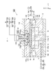
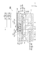
- FIG. 1 is a diagram schematically showing a plasma processing apparatus according to an embodiment.
- FIG. 1 shows a cross section of the plasma processing apparatus.
- a plasma processing apparatus 10 illustrated in FIG. 1 includes a processing container 12 and a stage 14.
- the processing container 12 defines a processing space S.
- the processing container 12 can be comprised with metals, such as stainless steel and aluminum.
- the processing container 12 includes a first side wall 16, a second side wall 18, a top plate part 20, and a bottom part 22.
- the first side wall 16 has a substantially cylindrical shape extending along the axis X.
- the inner space of the first side wall 16 is the processing space S.
- the second side wall 18 extends downward continuously from the first side wall 16.
- the second side wall 18 also has a substantially cylindrical shape extending along the axis X.
- a stage 14 is provided in the space inside the second side wall 18.
- a substrate to be processed W is placed on the upper surface (mounting surface) of the stage 14.
- the stage 14 can adsorb the substrate W to be processed by electrostatic force (static electricity / Coulomb force), for example.
- a processing space S exists above the stage 14.
- the plasma processing apparatus 10 may further include a support column 24 that extends below the stage 14. The support column 24 can support the stage 14.
- a space 18 a is formed in the second side wall 18.
- the space 18a can extend along an annular closed curve centered on the axis X.
- the second side wall 18 is formed with a hole 18b that connects the processing space S and the space 18a.
- the second side wall 18 is formed with a hole 18 c extending from the space 18 a to the outer surface of the second side wall 18.
- the plasma processing apparatus 10 may further include an exhaust device 26 connected to the hole 18c. The exhaust device 26 depressurizes and exhausts the processing space S.
- the second side wall 18 is provided with a gas path 18 d extending from the space between the outer periphery of the stage 14 and the second side wall 18 to the outer surface of the second side wall 18.
- a gas supply system 28 is connected to the gas path 18d.
- the gas supply system 28 supplies a purge gas to the processing space S.
- An inert gas such as argon is used as the purge gas.
- the gas supply system 28 includes a gas source 28a, a valve 28b, and a flow rate controller 28c.
- the gas source 28a is a purge gas source.
- the valve 28b is connected to the gas source 28a and switches supply and stop of supply of the purge gas from the gas source 28a.
- the flow rate controller 28c is, for example, a mass flow controller, and controls the flow rate of the purge gas to the processing space S.
- a bottom 22 is provided at the lower end of the second side wall 18.
- the upper end opening of the first side wall 16 is closed by the top plate portion 20.
- the top plate part 20 has conductivity, and defines the processing space S from above.
- the top plate portion 20 constitutes a shielding portion that separates a plasma generation space and a processing space S described later.
- the top plate unit 20 is provided with a first gas supply unit 30.
- the first gas supply unit 30 supplies a first process gas for atomic layer deposition to the processing space S.
- the first gas supply unit 30 may include a gas path 30a and a plurality of holes 30b.
- the gas path 30a may extend along an annular closed curve centered on the axis X.
- the plurality of holes 30b extend from the gas path 30a to the processing space S.
- the plasma processing apparatus 10 may further include a gas supply system 32, and the gas supply system 32 is connected to the gas path 30a.
- the gas supply system 32 may include a gas source 32a, a valve 32b, and a flow rate controller 32c.
- the gas source 32a is a gas source of the first process gas.
- the first process gas for example, a gas containing silicon atoms, for example, aminosilane such as BTBAS (Bistal Butylaminosilane) can be used.
- the valve 32b is connected to the gas source 32a and switches supply and stop of supply of gas from the gas source 32a.
- the flow rate controller 32 c is, for example, a mass flow controller, and controls the flow rate of the first process gas to the processing space S.
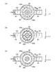
- FIG. 2A is a cross-sectional view taken along the line II-II in FIG.
- the plasma processing apparatus 10 may further include an upper plate portion 34 and a side plate portion 36. These upper plate part 34 and side plate part 36 also have conductivity.
- the upper plate portion 34 is provided above the top plate portion 20 so as to be separated from the top plate portion 20 and extends along a plane intersecting the axis X.
- the side plate portion 36 extends in the axis X direction and connects the upper plate portion 34 and the top plate portion 20.
- top plate portion 20, upper plate portion 34, and side plate portion 36 define spaces S1, S2, and S3.
- the space S2 is provided between the space S1 and the space S3 in the Y direction that intersects the axis X direction.
- the top plate portion 20, the upper plate portion 34, and the side plate portion 36 constitute a rectangular waveguide having the space S1 as an internal space.
- the plasma processing apparatus 10 can further include a microwave generator 38, which is connected to a rectangular waveguide.
- the microwave generator 38 supplies, for example, a 500 MHz microwave to the rectangular waveguide.
- the space S2 is a substantially disk-shaped space.
- the plasma processing apparatus 10 further includes a dielectric member 40, and the dielectric member 40 is provided in the space S2.
- a plunger 42 that is movable in the Y direction is provided.
- bumps 44 are provided in the space S1.
- the plunger 42 and the bump 44 face each other in the Y direction so that the dielectric member 40 is interposed therebetween.
- the plunger 42 and the bump 44 are made of metal, and a standing wave is generated between the plunger 42 and the bump 44.
- the standing wave (microwave) generated in this way is introduced into the dielectric member 40 accommodated in the space S2.
- the dielectric member 40 is a substantially disk-shaped member.
- the dielectric member 40 is made of a dielectric material such as quartz, for example.
- a plurality of cavities 40 a are formed in the dielectric member 40.
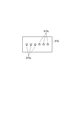
- the cavity 40a may have a cylindrical shape extending in the axis X direction. These cavities 40a may be arranged along a plurality of concentric circles about the axis X. In one embodiment, as shown in FIG. 2A, the plurality of cavities 40a are arranged along two concentric circles about the axis X. These cavities 40a may have, for example, a diameter of 10 to 30 mm and a depth of 10 to 30 mm (length in the axis X direction).
- a plurality of holes 46a are connected to the plurality of cavities 40a.
- the plurality of holes 46 a are formed across the dielectric member 40 and the upper plate portion 34.
- the plurality of holes 46 a are connected to a common gas path 46 b formed in the upper plate portion 34.
- the plurality of holes 46 a and the gas path 46 b constitute a second gas supply unit 46.
- the second gas supply unit 46 supplies the second process gas to the cavity 40a.
- the second gas supply unit 46 is connected to a gas supply system 48.
- the gas supply system 48 may include a gas source 48a, a valve 48b, and a flow controller 48c.
- the gas source 48a is a gas source of the second process gas.
- the valve 48b is connected to the gas source 48a and switches supply and stop of supply of the second process gas.
- the flow controller 48c is, for example, a mass flow controller, and switches the supply amount of the second process gas.
- a gas supply system 50 may be further connected to the second gas supply unit 46.
- the gas supply system 50 may include a gas source 50a, a valve 50b, and a flow rate controller 50c.
- the gas source 50a is a gas source of an inert gas such as argon.
- the valve 50b is connected to the gas source 50a and switches between supply and stop of supply of the inert gas.
- the flow controller 50c is a mass flow controller, for example, and switches the supply amount of the inert gas.
- the top plate portion 20 has a plurality of communication holes 20 a.
- the plurality of communication holes 20a connect the plurality of cavities 40a to the processing space S, respectively.
- These communication holes 20a extend from the lower surface (first surface) 20b of the top plate 20 to the upper surface (second surface) 20c.
- the upper surface 20c is opposed to the lower surface 20b.
- the lower surface 20b faces the processing space S.
- the dielectric member 40 is placed on the upper surface 20c so as to be in contact with the upper surface 20c.
- the second process gas is supplied to the cavity 40 a of the dielectric member 40. Further, microwaves are supplied to the cavity 40a of the dielectric member 40, and plasma is generated in the cavity 40a. Thereby, in the cavity 40a, the second process gas is activated and radicals are generated.
- the cavity 40 a that is, the plasma generation space is separated from the processing space S by the top plate part 20. Since the top plate portion 20 has conductivity, it functions as a shielding portion for plasma generated in the cavity 40a. In the plasma processing apparatus 10, since the plasma generation space and the processing space S are separated by the shielding portion, the capacity of the processing space S, particularly the distance from the shielding portion to the stage 14 can be reduced.
- the radicals are supplied from the cavity 40a into the processing space S through the communication hole 20a.
- the cavity 40a is provided immediately above the shielding part (top plate part 20)
- the distance between the processing space S and the cavity 40a is shortened. Therefore, the radical can be supplied to the processing space S while suppressing the deactivation of the radical generated in the cavity 40a. Therefore, the plasma processing apparatus 10 can shorten the plasma processing time.
- the distance from the shielding portion to the stage 14, that is, the length of the processing space S in the axis X direction can be shortened.
- the length of the processing space S in the axis X direction can be set to 5 mm to 40 mm.
- the shielding is performed so that the distance in the axis X direction between the placement surface (upper surface) and the lower surface (first surface) 20b of the stage 14 on which the substrate to be processed W is placed is 5 mm to 40 mm.
- a distance in the direction of the axis X between the top plate part 20 constituting the part and the stage 14 can be set.
- the substrate to be processed W is placed on the stage 14.
- the first process step is performed.
- the first process gas is supplied to the processing space S.
- the valve 32b is opened, and the flow rate of the first process gas is controlled by the flow rate controller 32c.
- the layer made of the atoms or molecules of the raw material contained in the first process gas is adsorbed on the substrate W to be processed. Further, unnecessary gas is exhausted by the exhaust device 26 in the first process step.
- the pressure in the processing space S in this step is, for example, 5 Torr (666.5 Pa).
- the valve 32b is closed.
- the first purge / evacuation step is performed.
- purge gas is supplied to the processing space S as required, and the processing space S is exhausted.
- the valve 28b is opened, and the supply amount of the purge gas is controlled by the flow rate controller 28c. Further, exhaust by the exhaust device 26 is performed.
- the purge gas may be supplied from the gas source 50a through the valve 50b through the flow rate control by the flow rate controller 50c.
- the first purge / evacuation step unnecessary portions (gas components) other than the layer formed in the first process step are removed.
- a portion for example, a single molecular layer or a single atomic layer
- the remaining portion (gas component) that is physically or chemically adsorbed to the substrate W to be processed is removed from the layer formed in (1).
- the atmosphere in the processing space S is replaced with an inert gas. As described above, since the capacity of the processing space S is small, this replacement can be completed in a relatively short time.
- the second process step is performed.
- a microwave is generated by the microwave generator 38, and further, a second process gas is supplied into the cavity 40a.
- the second process gas is supplied into the cavity 40a while opening the valve 48b and controlling the flow rate by the flow rate controller 48c.
- an inert gas may be supplied from the gas supply system 50.
- the pressure in the processing space S in this step is, for example, 5 Torr (666.5 Pa).
- the second process step plasma is generated in the cavity 40a by microwaves.
- the second process gas supplied into the cavity 40a is activated and radicals are generated.
- the generated radicals are supplied to the processing space S, and nitride or oxidize the layer deposited on the substrate W to be processed.
- a second purge / evacuation step is performed.
- purge gas is supplied to the processing space S and the processing space S is exhausted as necessary.
- the valve 28b is opened, and the supply amount of the purge gas is controlled by the flow rate controller 28c. Further, exhaust by the exhaust device 26 is performed.
- the purge gas may be supplied from the gas source 50a through the valve 50b through the flow rate control by the flow rate controller 50c.
- the first process step, the first purge / exhaust step, the second process step, and the second purge / exhaust step are repeated a predetermined number of times.
- an oxidized or nitrided atomic layer or molecular layer is formed on the substrate to be processed.
- the various control signals output by the control unit 52 include, for example, the exhaust device 26, the valve 28b, the flow rate controller 28c, the valve 32b, the flow rate controller 32c, the valve 48b, the flow rate controller 48c, the valve 50b, and the flow rate controller. Is output to 50c.
- the exhaust device 26, the valve 28b, the flow rate controller 28c, the valve 32b, the flow rate controller 32c, the valve 48b, the flow rate controller 48c, the valve 50b, and the flow rate controller 50c are the first process steps described above, Control is performed so as to shift to a state in the first purge / evacuation step, the second process step, and the second purge / evacuation step.
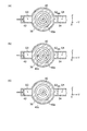
- FIG. 4 is a diagram illustrating a dielectric member according to another embodiment.
- the cavity 40a formed in the dielectric member 40 may be an annular groove formed along a plurality of concentric circles with the axis X as the center.
- the annular groove may have a width of 10-30 mm and a depth of 10-30 mm, for example.
- the plurality of cavities 40a configured as annular grooves may be communicated with each other by a communication path 40c.
- the upper plate portion 134 is made of metal and is provided on the top plate portion 120.
- the upper plate portion 134 and the top plate portion 120 define a substantially disk-shaped space between them. This space is along the axis X, and the dielectric member 140 is accommodated in the space.
- the dielectric member 140 has a cavity 140a.
- the cavity 140a may be one or more annular grooves, or may be one or more columnar spaces.
- the cavity 140a is connected to the processing space S through the communication hole 120a.
- the communication hole 120a extends from the lower surface 120b of the top plate portion 120 to the upper surface 120c.
- the dielectric member 140 is placed on the top plate portion 120 so as to be in contact with the upper surface 120c.
- the second gas supply unit 146 is connected to the cavity 140a.
- the second gas supply unit 146 is formed over the upper plate part 134 and the dielectric member 140, and constitutes a second process gas supply path.
- Gas supply systems 48 and 50 are connected to the second gas supply unit 146.
- the coaxial waveguide 154 includes an outer conductor 154a and an inner conductor 154b.
- the outer conductor 154a is a cylindrical conductor extending along the axis X. One end of the outer conductor 154 a is connected to the microwave generator 138, and the other end is connected to the upper plate part 134.
- the inner conductor 154b is a conductor extending along the axis X and passes through the inner hole of the outer conductor 154a. One end of the inner conductor 154 b is connected to the microwave generator 138, and the other end penetrates the upper plate portion 134 and the dielectric member 140 and is connected to the top plate portion 120.
- the microwave generated by the microwave generator 138 is supplied to the dielectric member 140 via the coaxial waveguide 154.
- the dielectric member 140 functions as a so-called slow wave plate.
- the microwave supplied to the dielectric member 140 generates plasma in the cavity 140a.
- the second process gas supplied into the cavity 140a is activated, and radicals are generated in the cavity 140a.
- the generated radical is supplied to the processing space S through the communication hole 120a.
- the plasma processing apparatus 100 can also be used for the ALD method.
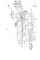
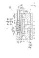
- FIG. 7 is a diagram schematically showing a plasma processing apparatus according to another embodiment.
- the plasma processing apparatus 200 shown in FIG. 7 is different from the plasma processing apparatus 10 in that a coaxial waveguide 254, a dielectric plate 256, and a slot plate 258 are provided.
- the plasma processing apparatus 200 includes a top plate portion 220, an upper plate portion 234, and a dielectric member 240 instead of the top plate portion 20, the upper plate portion 34, and the dielectric member 40.
- the top plate 220 is provided directly above the first side wall 16.
- the top plate part 220 defines the processing space S from above.
- the top plate part 220 has conductivity and functions as a shielding part.
- a first gas supply unit 230 is formed on the top plate unit 220.
- the first gas supply unit 230 may include a gas path 230a and a plurality of holes 230b.
- the gas path 230a may extend along an annular closed curve centered on the axis X.
- the plurality of holes 230b extend from the gas path 230a to the processing space S.
- a gas supply system 32 is connected to the gas path 230a.
- the upper plate portion 234 is made of metal and is provided on the top plate portion 220.
- the upper plate portion 234 and the top plate portion 220 define a substantially disk-shaped space between them. This space is along the axis X, and the dielectric member 240, the dielectric plate 256, and the slot plate 258 are accommodated in the space.
- the slot plate 258 is a conductor on a substantially circular plate.
- the slot plate 258 is formed with a plurality of slot pairs each including two slots extending in a direction intersecting or orthogonal to each other. These slot pairs are arranged at predetermined intervals in the radial direction around the center of the axis X, and are arranged at predetermined intervals in the circumferential direction.
- a dielectric plate 256 is provided between the slot plate 258 and the upper plate portion 234.
- the slot plate 258, the upper plate portion 234, and the dielectric plate 256 constitute a radial line slot antenna.
- the coaxial waveguide 254 includes an outer conductor 254a and an inner conductor 254b.
- the outer conductor 254a is a cylindrical conductor extending along the axis X.
- One end of the outer conductor 254a is connected to the mode converter 260.
- the mode converter 260 is connected to the microwave generator 238 via the waveguide 262 and the tuner 264.
- the other end of the outer conductor 254a is connected to the upper plate portion 234.
- the inner conductor 254b is a cylindrical conductor extending along the axis X and passes through the inner hole of the outer conductor 254a. One end of the inner conductor 254 b is connected to the mode converter 260, and the other end penetrates the upper plate part 134 and the dielectric plate 256 and is connected to the slot plate 258.
- a dielectric member 240 is provided between the slot plate 258 and the upper surface 220 c of the top plate portion 220.
- the dielectric member 240 has a function as a so-called dielectric window.
- a cavity 240a is formed in the dielectric member 240.
- the cavity 240a may be one or more annular grooves, or may be one or more columnar spaces.
- the cavity 240a is connected to the processing space S through the communication hole 220a.
- the communication hole 220a extends from the lower surface 220b of the top plate portion 220 to the upper surface 220c.
- the dielectric member 240 is placed on the top plate portion 220 so as to be in contact with the upper surface 220c.
- the second gas supply unit 246 is connected to the cavity 240a.
- the second gas supply unit 246 is formed inside the dielectric member 240.
- the second gas supply unit 246 is connected to the gas supply systems 48 and 50 through the inner hole of the inner conductor 254b.
- the microwave supplied to the dielectric member 240 generates plasma in the cavity 240a.
- the second process gas supplied into the cavity 240a is activated, and radicals are generated in the cavity 240a.
- the generated radical is supplied to the processing space S through the communication hole 220a.
- the plasma processing apparatus 200 can also be used for the ALD method.
- a plasma processing apparatus 300 illustrated in FIG. 8 includes a processing container 312 and a stage 14.
- the processing container 312 defines a processing space S.
- the processing container 312 is made of metal and includes a side wall 318, a top plate part 320, and a bottom part 322.
- the side wall 318 has a substantially cylindrical shape extending along the axis X. The upper end opening of the side wall 318 is closed by the top plate part 320.
- a bottom 322 is provided at the lower end of the side wall 318.
- a stage 14 is provided in the inner space of the side wall 318, and the stage 14 is supported by a column 24 provided below the stage 14.
- a processing space S exists above the stage 14.
- a first gas supply unit 330 is formed on the top plate unit 320.
- the first gas supply unit 330 includes a space 330 a formed in the top plate 320, a hole 330 b that connects the space 330 a and the processing space S, and a gas path 330 c that connects the space 330 a to the outside of the processing container 312. Contains.
- a gas supply system 32 is connected to the gas path 330c.
- FIG. 9 is a plan view showing a shielding part of the plasma processing apparatus shown in FIG.
- description will be made with reference to FIG. 9 together with FIG.
- the shielding part 370 has conductivity and has a plate shape.
- the shielding part 370 includes a first surface 370a and a second surface 370b.
- the first surface 370a faces the processing space S.
- the distance between the first surface 370a and the stage 14 for example, the shortest distance (distance in the Y direction) between the first surface 370a and the edge of the substrate W to be processed placed on the stage 14 is 5. It can be set to be ⁇ 60 mm. By such distance setting, the processing time of the plasma processing can be further shortened.
- the second surface 370b is a surface on the opposite side to the first surface 370a.
- the shielding portion 370 is formed with a communication hole 370c extending from the first surface 370a to the second surface 370b. In one embodiment, a plurality of communication holes 370 c are formed in the shielding part 370.
- Dielectric member 340 is provided in contact with second surface 370b of shielding portion 370.
- the dielectric member 340 is provided outside the shielding portion 370 with respect to the axis X.
- the dielectric member 340 is provided with a cavity 340a.
- the cavity 340a communicates with the processing space S through the communication hole 370c.
- the dielectric member 340 and the shielding part 370 are embedded in the side wall 318 and the top plate part 320.
- a second gas supply unit 346 connected to the cavity 340 a of the dielectric member 340 is formed.
- the second gas supply unit 346 may be a gas path formed in the processing container 312.
- Gas supply systems 48 and 50 are connected to the second gas supply unit 346.
- a waveguide 372 is attached to the outer surface of the processing container 312.
- a microwave generator 338 is connected to the waveguide 372.
- the microwave generated by the microwave generator 338 is introduced into the cavity 340 a of the dielectric member 340 through the waveguide 372 and the dielectric member 340.
- the second process gas is supplied to the cavity 340a. Thereby, in the cavity 340a, the second process gas is activated and radicals are generated. The generated radicals are supplied to the processing space S.
- the distance between the cavity 340a and the processing space S is short. Therefore, radicals can be supplied to the processing space S while suppressing the amount of deactivation. Therefore, the plasma processing apparatus 300 can also shorten the processing time of the plasma processing (second process step).
- FIG. 10 is a diagram schematically showing a plasma processing apparatus according to another embodiment.
- a plasma processing apparatus 400 shown in FIG. 10 includes a waveguide 472 as a means for introducing a microwave. Further, the plasma processing apparatus 400 includes a top plate portion 420 and a dielectric member 440 instead of the top plate portion 20 and the dielectric member 40.
- the top plate 420 is provided directly above the first side wall 16.
- the top plate portion 420 defines the processing space S from above.
- the top plate portion 420 has conductivity and functions as a shielding portion.
- a first gas supply unit 430 is formed on the top plate unit 420.
- the first gas supply unit 430 may include a gas path 430a and a plurality of holes 430b.
- the gas path 430a may extend along an annular closed curve about the axis X.
- the plurality of holes 430b extend from the gas path 430a to the processing space S.
- a gas supply system 32 is connected to the gas path 430a.
- the plasma processing apparatus 400 further includes an upper plate portion 434.
- the upper plate portion 434 is made of metal and is provided on the top plate portion 420.
- the upper plate portion 434 and the top plate portion 420 define a substantially disc-shaped space between them. This space is along the axis X, and the dielectric member 440 is accommodated in the space.
- a cavity 440a is formed in the dielectric member 440.
- the cavity 440a may be one or more annular grooves, or may be one or more columnar spaces.
- the cavity 440a is connected to the processing space S through the communication hole 420a.
- the communication hole 420a extends from the lower surface 420b of the top plate portion 420 to the upper surface 420c.
- the dielectric member 440 is placed on the top plate 420 so as to be in contact with the upper surface 420c.
- the second gas supply unit 446 is connected to the cavity 440a.
- the second gas supply part 446 is formed over the upper plate part 434 and the dielectric member 440, and constitutes a second process gas supply path.
- Gas supply systems 48 and 50 are connected to the second gas supply unit 446.
- a waveguide 472 is provided on the dielectric member 440.
- the waveguide 472 includes a first waveguide 472a and a second waveguide 472b.
- the first waveguide portion 472a constitutes a rectangular waveguide extending in a direction intersecting the axis X.
- a microwave generator 438 is connected to one end of the first waveguide 472a.
- the second waveguide 472b is connected to the other end of the first waveguide 472a.
- the second waveguide 472b is placed on the dielectric member 440.
- the second waveguide portion 472b constitutes a waveguide extending along an annular closed curve with the axis X as the center.
- a plurality of slots 472c are formed in the lower wall portion of the second waveguide portion 472b. These slots 472c are arranged in the circumferential direction.
- slot 472c may be provided over cavity 440a in the axis X direction. Thereby, the plasma generation efficiency in the cavity 440a is increased.
- the microwave generated by the microwave generator 438 is supplied to the dielectric member 440.
- the microwave supplied to the dielectric member 440 generates plasma in the cavity 440a.
- the second process gas supplied into the cavity 440a is activated, and radicals are generated in the cavity 440a.
- the generated radical is supplied to the processing space S through the communication hole 420a.
- the plasma processing apparatus 400 can also be used for the ALD method.
- FIG. 11 is a diagram schematically showing a plasma processing apparatus according to another embodiment.
- a plasma processing apparatus 500 shown in FIG. 11 includes a waveguide 572 as a means for introducing a microwave.
- the plasma processing apparatus 500 includes a top plate portion 520 and a dielectric member 540 instead of the top plate portion 20 and the dielectric member 40.
- the top plate portion 520 is provided immediately above the first side wall 16.
- the top plate portion 520 defines the processing space S from above.
- the top plate portion 520 has conductivity and functions as a shielding portion.
- a first gas supply unit 530 is formed on the top plate unit 520.
- the fifth gas supply unit 430 may include a gas path 530a and a plurality of holes 530b.
- the gas path 530a may extend along an annular closed curve about the axis X.
- the plurality of holes 530b extend from the gas path 530a to the processing space S.
- a gas supply system 32 is connected to the gas path 530a.
- the plasma processing apparatus 500 further includes an upper plate portion 534.
- the upper plate portion 534 is made of metal and is provided on the top plate portion 520.
- the upper plate portion 534 and the top plate portion 520 define a substantially disc-shaped space between them. This space is along the axis X, and the dielectric member 540 is accommodated in the space.
- the dielectric member 540 has a cavity 540a.
- the cavity 540a may be one or more annular grooves, or may be one or more columnar spaces.
- the cavity 540a is connected to the processing space S through the communication hole 520a.
- the communication hole 520a extends from the lower surface 520b of the top plate portion 520 to the upper surface 520c.
- the dielectric member 540 is placed on the top plate portion 520 so as to be in contact with the upper surface 520c.
- the second gas supply unit 546 is connected to the cavity 540a.
- the second gas supply part 546 is formed over the upper plate part 534 and the dielectric member 540, and constitutes a second process gas supply path.
- Gas supply systems 48 and 50 are connected to the second gas supply unit 546.
- a waveguide 572 is provided on the top plate portion 520.
- the waveguide 572 includes a first waveguide 572a and a second waveguide 572b.
- the first waveguide portion 572a constitutes a rectangular waveguide extending in a direction intersecting the axis X.
- a microwave generator 538 is connected to one end of the first waveguide 572a.
- the second waveguide 572b is connected to the other end of the first waveguide 572a.
- the second waveguide 572b constitutes a waveguide extending along an annular closed curve with the axis X as the center.
- the second waveguide portion 572 b is provided so as to surround the outer peripheral surface of the dielectric member 540.
- a plurality of slots 572c are formed in the inner wall portion of the second waveguide portion 572b. These slots 572c are arranged in the circumferential direction.
- the microwave generated by the microwave generator 538 is supplied to the dielectric member 540.
- the microwave supplied to the dielectric member 540 generates plasma in the cavity 540a.
- the second process gas supplied into the cavity 540a is activated, and radicals are generated in the cavity 540a.
- the generated radical is supplied to the processing space S through the communication hole 520a.
- the plasma processing apparatus 500 can also be used for the ALD method.
- DESCRIPTION OF SYMBOLS 10 Plasma processing apparatus, 12 ... Processing container, 14 ... Stage, 20 ... Shielding part (top plate part), 20a ... Communication hole, 20b ... Lower surface (1st surface), 20c ... Upper surface (2nd surface), DESCRIPTION OF SYMBOLS 30 ... 1st gas supply part, 40 ... Dielectric member, 40a ... Cavity, 40c ... Communication path, 46 ... 2nd gas supply part, S ... Processing space.
Landscapes
- Chemical & Material Sciences (AREA)
- Engineering & Computer Science (AREA)
- Physics & Mathematics (AREA)
- Plasma & Fusion (AREA)
- Analytical Chemistry (AREA)
- Materials Engineering (AREA)
- Chemical Kinetics & Catalysis (AREA)
- Mechanical Engineering (AREA)
- Metallurgy (AREA)
- Organic Chemistry (AREA)
- General Chemical & Material Sciences (AREA)
- Electromagnetism (AREA)
- Plasma Technology (AREA)
- Drying Of Semiconductors (AREA)
- Chemical Vapour Deposition (AREA)
Abstract
Description
本発明の一側面に係るプラズマ処理装置は、ステージ、処理容器、第1の供給手段、遮蔽部、誘電体部材、マイクロ波導入手段、及び、第2の供給手段を備えている。ステージは、被処理基体を搭載する。処理容器は、ステージの上方に処理空間を画成する。第1の供給手段は、処理空間に層堆積用の第1のプロセスガスを供給する。遮蔽部は、導電性を有し、処理空間に面する第1の面、及び、当該第1の面と反対側の第2の面を有する。遮蔽部には、第1の面から第2の面まで延在する一以上の連通孔が設けられている。誘電体部材は、遮蔽部の第2の面に接するように設けられている。誘電体部材には、一以上の連通孔に接続する一以上の空洞が設けられている。マイクロ波導入手段は、誘電体部材にマイクロ波を導入する。第2の供給手段は、誘電体部材の空洞内にプラズマ処理用の第2のプロセスガスを供給する。
Claims (12)
- ステージと、
前記ステージの上方に処理空間を画成する処理容器と、
前記処理空間に層堆積用の第1のプロセスガスを供給する第1の供給手段と、
前記処理空間に面する第1の面、及び、該第1の面と反対側の第2の面を有し、導電性を有し、前記第1の面から前記第2の面まで延在する一以上の連通孔が設けられた遮蔽部と、
前記遮蔽部の前記第2の面に接するように設け、前記一以上の連通孔に接続する一以上の空洞が設けられた誘電体部材と、
前記誘電体部材にマイクロ波を導入するマイクロ波導入手段と、
前記誘電体部材の前記空洞内にプラズマ処理用の第2のプロセスガスを供給する第2の供給手段と、
を備えるプラズマ処理装置。 - 前記一以上の空洞は、前記誘電体部材に形成された柱状の空間である、請求項1に記載のプラズマ処理装置。
- 前記一以上の空洞は、前記誘電体部材に形成された環状の溝である、請求項1に記載のプラズマ処理装置。
- 前記誘電体部材には、複数の前記空洞のうち少なくとも二つの間を連通する連通路が形成されている、請求項1~3の何れか一項に記載のプラズマ処理装置。
- 前記マイクロ波導入手段は、同軸導波管を含む、請求項1~4の何れか一項に記載のプラズマ処理装置。
- 前記同軸導波管は、前記誘電体部材を通過して前記遮蔽部に結合されている、請求項5に記載のプラズマ処理装置。
- 前記マイクロ波導入手段は、前記同軸導波管に結合された金属製のスロット板であって、周方向及び径方向に複数のスロットが形成された該スロット板を含み、
前記誘電体部材は、前記スロット板と前記遮蔽部との間に設けられ、マイクロ波透過する誘電体窓を構成する、
請求項5に記載のプラズマ処理装置。 - 前記一以上の連通孔の各々の断面積は、前記一以上の空洞の断面積よりも小さい、請求項1~7の何れか一項に記載のプラズマ処理装置。
- 一つの前記空洞に対して複数の前記連通孔が接続されている、請求項1~8の何れか一項に記載のプラズマ処理装置。
- 被処理基体を載置するための前記ステージの載置面と前記第1の面との間の距離が5mm~40mmである、請求項1~9の何れか一項に記載のプラズマ処理装置。
- 前記遮蔽部及び前記誘電体部材は、前記処理空間の側方に設けられている、請求項1に記載のプラズマ処理装置。
- 前記第1の面と前記ステージ上に搭載される被処理基体のエッジとの最短距離が5mm~60mmであるように、前記ステージと前記第1の面との間の距離が設定されている、請求項11に記載のプラズマ処理装置。
Priority Applications (2)
| Application Number | Priority Date | Filing Date | Title |
|---|---|---|---|
| US14/118,993 US9670584B2 (en) | 2011-05-23 | 2012-05-21 | Plasma processing device |
| KR1020137030373A KR20140031902A (ko) | 2011-05-23 | 2012-05-21 | 플라즈마 처리 장치 |
Applications Claiming Priority (2)
| Application Number | Priority Date | Filing Date | Title |
|---|---|---|---|
| JP2011-114657 | 2011-05-23 | ||
| JP2011114657A JP5563522B2 (ja) | 2011-05-23 | 2011-05-23 | プラズマ処理装置 |
Publications (1)
| Publication Number | Publication Date |
|---|---|
| WO2012161164A1 true WO2012161164A1 (ja) | 2012-11-29 |
Family
ID=47217241
Family Applications (1)
| Application Number | Title | Priority Date | Filing Date |
|---|---|---|---|
| PCT/JP2012/062955 Ceased WO2012161164A1 (ja) | 2011-05-23 | 2012-05-21 | プラズマ処理装置 |
Country Status (5)
| Country | Link |
|---|---|
| US (1) | US9670584B2 (ja) |
| JP (1) | JP5563522B2 (ja) |
| KR (1) | KR20140031902A (ja) |
| TW (1) | TW201320832A (ja) |
| WO (1) | WO2012161164A1 (ja) |
Families Citing this family (88)
| Publication number | Priority date | Publication date | Assignee | Title |
|---|---|---|---|---|
| US10283321B2 (en) | 2011-01-18 | 2019-05-07 | Applied Materials, Inc. | Semiconductor processing system and methods using capacitively coupled plasma |
| US9064815B2 (en) | 2011-03-14 | 2015-06-23 | Applied Materials, Inc. | Methods for etch of metal and metal-oxide films |
| US9267739B2 (en) | 2012-07-18 | 2016-02-23 | Applied Materials, Inc. | Pedestal with multi-zone temperature control and multiple purge capabilities |
| US9373517B2 (en) | 2012-08-02 | 2016-06-21 | Applied Materials, Inc. | Semiconductor processing with DC assisted RF power for improved control |
| US9132436B2 (en) | 2012-09-21 | 2015-09-15 | Applied Materials, Inc. | Chemical control features in wafer process equipment |
| US10256079B2 (en) | 2013-02-08 | 2019-04-09 | Applied Materials, Inc. | Semiconductor processing systems having multiple plasma configurations |
| US9309598B2 (en) | 2014-05-28 | 2016-04-12 | Applied Materials, Inc. | Oxide and metal removal |
| US9355922B2 (en) | 2014-10-14 | 2016-05-31 | Applied Materials, Inc. | Systems and methods for internal surface conditioning in plasma processing equipment |
| US9966240B2 (en) | 2014-10-14 | 2018-05-08 | Applied Materials, Inc. | Systems and methods for internal surface conditioning assessment in plasma processing equipment |
| US11637002B2 (en) | 2014-11-26 | 2023-04-25 | Applied Materials, Inc. | Methods and systems to enhance process uniformity |
| US10573496B2 (en) * | 2014-12-09 | 2020-02-25 | Applied Materials, Inc. | Direct outlet toroidal plasma source |
| US10224210B2 (en) | 2014-12-09 | 2019-03-05 | Applied Materials, Inc. | Plasma processing system with direct outlet toroidal plasma source |
| US11257693B2 (en) | 2015-01-09 | 2022-02-22 | Applied Materials, Inc. | Methods and systems to improve pedestal temperature control |
| US9728437B2 (en) | 2015-02-03 | 2017-08-08 | Applied Materials, Inc. | High temperature chuck for plasma processing systems |
| US20160225652A1 (en) | 2015-02-03 | 2016-08-04 | Applied Materials, Inc. | Low temperature chuck for plasma processing systems |
| JP6563717B2 (ja) * | 2015-07-10 | 2019-08-21 | 東芝三菱電機産業システム株式会社 | 成膜装置 |
| US9691645B2 (en) | 2015-08-06 | 2017-06-27 | Applied Materials, Inc. | Bolted wafer chuck thermal management systems and methods for wafer processing systems |
| US9741593B2 (en) | 2015-08-06 | 2017-08-22 | Applied Materials, Inc. | Thermal management systems and methods for wafer processing systems |
| US9349605B1 (en) | 2015-08-07 | 2016-05-24 | Applied Materials, Inc. | Oxide etch selectivity systems and methods |
| US10504700B2 (en) | 2015-08-27 | 2019-12-10 | Applied Materials, Inc. | Plasma etching systems and methods with secondary plasma injection |
| KR102619949B1 (ko) | 2016-05-16 | 2024-01-03 | 삼성전자주식회사 | 안테나, 그를 포함하는 마이크로파 플라즈마 소스, 플라즈마 처리 장치 |
| US10522371B2 (en) | 2016-05-19 | 2019-12-31 | Applied Materials, Inc. | Systems and methods for improved semiconductor etching and component protection |
| US10504754B2 (en) | 2016-05-19 | 2019-12-10 | Applied Materials, Inc. | Systems and methods for improved semiconductor etching and component protection |
| US9865484B1 (en) | 2016-06-29 | 2018-01-09 | Applied Materials, Inc. | Selective etch using material modification and RF pulsing |
| US10629473B2 (en) | 2016-09-09 | 2020-04-21 | Applied Materials, Inc. | Footing removal for nitride spacer |
| US10062575B2 (en) | 2016-09-09 | 2018-08-28 | Applied Materials, Inc. | Poly directional etch by oxidation |
| US10546729B2 (en) | 2016-10-04 | 2020-01-28 | Applied Materials, Inc. | Dual-channel showerhead with improved profile |
| US10062585B2 (en) | 2016-10-04 | 2018-08-28 | Applied Materials, Inc. | Oxygen compatible plasma source |
| US9934942B1 (en) | 2016-10-04 | 2018-04-03 | Applied Materials, Inc. | Chamber with flow-through source |
| US10062579B2 (en) | 2016-10-07 | 2018-08-28 | Applied Materials, Inc. | Selective SiN lateral recess |
| US9947549B1 (en) | 2016-10-10 | 2018-04-17 | Applied Materials, Inc. | Cobalt-containing material removal |
| US10163696B2 (en) | 2016-11-11 | 2018-12-25 | Applied Materials, Inc. | Selective cobalt removal for bottom up gapfill |
| US9768034B1 (en) | 2016-11-11 | 2017-09-19 | Applied Materials, Inc. | Removal methods for high aspect ratio structures |
| US10026621B2 (en) | 2016-11-14 | 2018-07-17 | Applied Materials, Inc. | SiN spacer profile patterning |
| US10242908B2 (en) | 2016-11-14 | 2019-03-26 | Applied Materials, Inc. | Airgap formation with damage-free copper |
| US10566206B2 (en) | 2016-12-27 | 2020-02-18 | Applied Materials, Inc. | Systems and methods for anisotropic material breakthrough |
| US10431429B2 (en) | 2017-02-03 | 2019-10-01 | Applied Materials, Inc. | Systems and methods for radial and azimuthal control of plasma uniformity |
| US10403507B2 (en) | 2017-02-03 | 2019-09-03 | Applied Materials, Inc. | Shaped etch profile with oxidation |
| US10043684B1 (en) | 2017-02-06 | 2018-08-07 | Applied Materials, Inc. | Self-limiting atomic thermal etching systems and methods |
| US10319739B2 (en) | 2017-02-08 | 2019-06-11 | Applied Materials, Inc. | Accommodating imperfectly aligned memory holes |
| US10943834B2 (en) | 2017-03-13 | 2021-03-09 | Applied Materials, Inc. | Replacement contact process |
| US10319649B2 (en) | 2017-04-11 | 2019-06-11 | Applied Materials, Inc. | Optical emission spectroscopy (OES) for remote plasma monitoring |
| US11276559B2 (en) | 2017-05-17 | 2022-03-15 | Applied Materials, Inc. | Semiconductor processing chamber for multiple precursor flow |
| JP7176860B6 (ja) | 2017-05-17 | 2022-12-16 | アプライド マテリアルズ インコーポレイテッド | 前駆体の流れを改善する半導体処理チャンバ |
| US11276590B2 (en) | 2017-05-17 | 2022-03-15 | Applied Materials, Inc. | Multi-zone semiconductor substrate supports |
| US10497579B2 (en) | 2017-05-31 | 2019-12-03 | Applied Materials, Inc. | Water-free etching methods |
| US10049891B1 (en) | 2017-05-31 | 2018-08-14 | Applied Materials, Inc. | Selective in situ cobalt residue removal |
| US10920320B2 (en) | 2017-06-16 | 2021-02-16 | Applied Materials, Inc. | Plasma health determination in semiconductor substrate processing reactors |
| US10541246B2 (en) | 2017-06-26 | 2020-01-21 | Applied Materials, Inc. | 3D flash memory cells which discourage cross-cell electrical tunneling |
| US10727080B2 (en) | 2017-07-07 | 2020-07-28 | Applied Materials, Inc. | Tantalum-containing material removal |
| US10541184B2 (en) | 2017-07-11 | 2020-01-21 | Applied Materials, Inc. | Optical emission spectroscopic techniques for monitoring etching |
| US10354889B2 (en) | 2017-07-17 | 2019-07-16 | Applied Materials, Inc. | Non-halogen etching of silicon-containing materials |
| US10043674B1 (en) | 2017-08-04 | 2018-08-07 | Applied Materials, Inc. | Germanium etching systems and methods |
| US10170336B1 (en) | 2017-08-04 | 2019-01-01 | Applied Materials, Inc. | Methods for anisotropic control of selective silicon removal |
| US10297458B2 (en) | 2017-08-07 | 2019-05-21 | Applied Materials, Inc. | Process window widening using coated parts in plasma etch processes |
| US10283324B1 (en) | 2017-10-24 | 2019-05-07 | Applied Materials, Inc. | Oxygen treatment for nitride etching |
| US10128086B1 (en) | 2017-10-24 | 2018-11-13 | Applied Materials, Inc. | Silicon pretreatment for nitride removal |
| US10256112B1 (en) | 2017-12-08 | 2019-04-09 | Applied Materials, Inc. | Selective tungsten removal |
| US10903054B2 (en) | 2017-12-19 | 2021-01-26 | Applied Materials, Inc. | Multi-zone gas distribution systems and methods |
| US11328909B2 (en) | 2017-12-22 | 2022-05-10 | Applied Materials, Inc. | Chamber conditioning and removal processes |
| US10854426B2 (en) | 2018-01-08 | 2020-12-01 | Applied Materials, Inc. | Metal recess for semiconductor structures |
| US10679870B2 (en) | 2018-02-15 | 2020-06-09 | Applied Materials, Inc. | Semiconductor processing chamber multistage mixing apparatus |
| US10964512B2 (en) | 2018-02-15 | 2021-03-30 | Applied Materials, Inc. | Semiconductor processing chamber multistage mixing apparatus and methods |
| TWI766433B (zh) | 2018-02-28 | 2022-06-01 | 美商應用材料股份有限公司 | 形成氣隙的系統及方法 |
| US10593560B2 (en) | 2018-03-01 | 2020-03-17 | Applied Materials, Inc. | Magnetic induction plasma source for semiconductor processes and equipment |
| US10319600B1 (en) | 2018-03-12 | 2019-06-11 | Applied Materials, Inc. | Thermal silicon etch |
| US10497573B2 (en) | 2018-03-13 | 2019-12-03 | Applied Materials, Inc. | Selective atomic layer etching of semiconductor materials |
| US10573527B2 (en) | 2018-04-06 | 2020-02-25 | Applied Materials, Inc. | Gas-phase selective etching systems and methods |
| US20190311887A1 (en) * | 2018-04-06 | 2019-10-10 | Applied Materials, Inc. | Multizone gas distribution apparatus |
| US10490406B2 (en) | 2018-04-10 | 2019-11-26 | Appled Materials, Inc. | Systems and methods for material breakthrough |
| US10699879B2 (en) | 2018-04-17 | 2020-06-30 | Applied Materials, Inc. | Two piece electrode assembly with gap for plasma control |
| US11393661B2 (en) | 2018-04-20 | 2022-07-19 | Applied Materials, Inc. | Remote modular high-frequency source |
| US10886137B2 (en) | 2018-04-30 | 2021-01-05 | Applied Materials, Inc. | Selective nitride removal |
| US10755941B2 (en) | 2018-07-06 | 2020-08-25 | Applied Materials, Inc. | Self-limiting selective etching systems and methods |
| US10872778B2 (en) | 2018-07-06 | 2020-12-22 | Applied Materials, Inc. | Systems and methods utilizing solid-phase etchants |
| US10672642B2 (en) | 2018-07-24 | 2020-06-02 | Applied Materials, Inc. | Systems and methods for pedestal configuration |
| US11049755B2 (en) | 2018-09-14 | 2021-06-29 | Applied Materials, Inc. | Semiconductor substrate supports with embedded RF shield |
| US10892198B2 (en) | 2018-09-14 | 2021-01-12 | Applied Materials, Inc. | Systems and methods for improved performance in semiconductor processing |
| US11062887B2 (en) | 2018-09-17 | 2021-07-13 | Applied Materials, Inc. | High temperature RF heater pedestals |
| US11417534B2 (en) | 2018-09-21 | 2022-08-16 | Applied Materials, Inc. | Selective material removal |
| US11682560B2 (en) | 2018-10-11 | 2023-06-20 | Applied Materials, Inc. | Systems and methods for hafnium-containing film removal |
| US11121002B2 (en) | 2018-10-24 | 2021-09-14 | Applied Materials, Inc. | Systems and methods for etching metals and metal derivatives |
| US11437242B2 (en) | 2018-11-27 | 2022-09-06 | Applied Materials, Inc. | Selective removal of silicon-containing materials |
| US11721527B2 (en) | 2019-01-07 | 2023-08-08 | Applied Materials, Inc. | Processing chamber mixing systems |
| US10920319B2 (en) | 2019-01-11 | 2021-02-16 | Applied Materials, Inc. | Ceramic showerheads with conductive electrodes |
| CN110791747A (zh) * | 2019-10-15 | 2020-02-14 | 江苏卓高新材料科技有限公司 | 一种用于薄膜材料表面沉积的沉积装置及沉积方法 |
| EP3964608A1 (de) * | 2020-09-02 | 2022-03-09 | Siemens Aktiengesellschaft | Direkte beschichtung einer membran mit einem katalysator |
| US20220415617A1 (en) * | 2021-06-25 | 2022-12-29 | Applied Materials, Inc. | Remote plasma apparatus for generating high-power density microwave plasma |
Citations (3)
| Publication number | Priority date | Publication date | Assignee | Title |
|---|---|---|---|---|
| JPS6423537A (en) * | 1987-07-20 | 1989-01-26 | Hitachi Ltd | Plasma processing device |
| JPH08124861A (ja) * | 1994-10-25 | 1996-05-17 | Sumitomo Metal Ind Ltd | プラズマ装置 |
| JP2009231611A (ja) * | 2008-03-24 | 2009-10-08 | Tokyo Electron Ltd | シャワープレート及びシャワープレートの製造方法 |
Family Cites Families (11)
| Publication number | Priority date | Publication date | Assignee | Title |
|---|---|---|---|---|
| US5804033A (en) * | 1990-09-26 | 1998-09-08 | Hitachi, Ltd. | Microwave plasma processing method and apparatus |
| EP0578047B1 (en) * | 1992-06-23 | 1998-05-13 | Nippon Telegraph And Telephone Corporation | Plasma processing apparatus |
| WO1999049705A1 (en) * | 1998-03-20 | 1999-09-30 | Tokyo Electron Limited | Plasma processing apparatus |
| AT408155B (de) * | 1999-02-17 | 2001-09-25 | Egston Eggenburger Syst Elektr | Schaltungsanordnung zur erzeugung einer versorgungsspannung |
| US6911391B2 (en) | 2002-01-26 | 2005-06-28 | Applied Materials, Inc. | Integration of titanium and titanium nitride layers |
| JP4179041B2 (ja) * | 2003-04-30 | 2008-11-12 | 株式会社島津製作所 | 有機el用保護膜の成膜装置、製造方法および有機el素子 |
| US8486845B2 (en) | 2005-03-21 | 2013-07-16 | Tokyo Electron Limited | Plasma enhanced atomic layer deposition system and method |
| JP5463536B2 (ja) * | 2006-07-20 | 2014-04-09 | 北陸成型工業株式会社 | シャワープレート及びその製造方法、並びにそのシャワープレートを用いたプラズマ処理装置、プラズマ処理方法及び電子装置の製造方法 |
| JP2008124424A (ja) * | 2006-10-16 | 2008-05-29 | Tokyo Electron Ltd | プラズマ成膜装置及びプラズマ成膜方法 |
| JP4960193B2 (ja) | 2007-10-12 | 2012-06-27 | 株式会社アルバック | 半導体装置の製造方法及び半導体装置の製造装置 |
| JP2010016225A (ja) * | 2008-07-04 | 2010-01-21 | Tokyo Electron Ltd | 温度調節機構および温度調節機構を用いた半導体製造装置 |
-
2011
- 2011-05-23 JP JP2011114657A patent/JP5563522B2/ja not_active Expired - Fee Related
-
2012
- 2012-05-21 KR KR1020137030373A patent/KR20140031902A/ko not_active Abandoned
- 2012-05-21 US US14/118,993 patent/US9670584B2/en not_active Expired - Fee Related
- 2012-05-21 WO PCT/JP2012/062955 patent/WO2012161164A1/ja not_active Ceased
- 2012-05-23 TW TW101118381A patent/TW201320832A/zh unknown
Patent Citations (3)
| Publication number | Priority date | Publication date | Assignee | Title |
|---|---|---|---|---|
| JPS6423537A (en) * | 1987-07-20 | 1989-01-26 | Hitachi Ltd | Plasma processing device |
| JPH08124861A (ja) * | 1994-10-25 | 1996-05-17 | Sumitomo Metal Ind Ltd | プラズマ装置 |
| JP2009231611A (ja) * | 2008-03-24 | 2009-10-08 | Tokyo Electron Ltd | シャワープレート及びシャワープレートの製造方法 |
Also Published As
| Publication number | Publication date |
|---|---|
| JP2012244045A (ja) | 2012-12-10 |
| US20140102367A1 (en) | 2014-04-17 |
| KR20140031902A (ko) | 2014-03-13 |
| JP5563522B2 (ja) | 2014-07-30 |
| US9670584B2 (en) | 2017-06-06 |
| TW201320832A (zh) | 2013-05-16 |
Similar Documents
| Publication | Publication Date | Title |
|---|---|---|
| JP5563522B2 (ja) | プラズマ処理装置 | |
| KR102728536B1 (ko) | 기판 처리 장치 및 기판 처리 방법 | |
| KR102255120B1 (ko) | 플라스마 생성 방법 및 이를 이용한 플라스마 처리 방법, 그리고 플라스마 처리 장치 | |
| JP6750534B2 (ja) | 成膜装置 | |
| JP5740203B2 (ja) | プラズマ処理装置及びその処理ガス供給構造 | |
| JP2021091968A (ja) | 基板処理装置、べベルマスク、基板処理方法 | |
| KR101943691B1 (ko) | 성막 장치 및 샤워 헤드 | |
| KR102114922B1 (ko) | 플라즈마 처리 방법 | |
| JP6767844B2 (ja) | 成膜装置及び成膜方法 | |
| TWI860465B (zh) | 電漿處理裝置 | |
| WO2015141521A1 (ja) | 基板処理装置、半導体装置の製造方法及び記録媒体 | |
| JP2017073535A (ja) | 被処理体を処理する方法 | |
| KR20110072336A (ko) | 기판처리장치 | |
| JP6896912B2 (ja) | バッチ式基板処理装置 | |
| CN112838004B (zh) | 蚀刻方法以及蚀刻装置 | |
| US10121680B2 (en) | Substrate processing apparatus | |
| KR102935543B1 (ko) | 기판 프로세싱을 위한 산화 프로파일의 변조 | |
| KR102185192B1 (ko) | 플라즈마 에칭 방법 | |
| TWI879211B (zh) | 電漿處理裝置及半導體裝置之製造方法 | |
| KR20230127373A (ko) | 피처리체를 처리하는 방법 | |
| KR20250179929A (ko) | 기판 처리 장치 | |
| JP7586599B2 (ja) | 成膜装置及び成膜方法 | |
| KR102930276B1 (ko) | ALD (Atomic Layer Deposition) 기판 프로세싱 챔버들의 막 특성들을 조절하기 위한 페데스탈들 | |
| KR20250174317A (ko) | 기판 처리 장치 | |
| JP2026510514A (ja) | 安定したテープフレーム基板処理のための金属シールド |
Legal Events
| Date | Code | Title | Description |
|---|---|---|---|
| 121 | Ep: the epo has been informed by wipo that ep was designated in this application |
Ref document number: 12789350 Country of ref document: EP Kind code of ref document: A1 |
|
| ENP | Entry into the national phase |
Ref document number: 20137030373 Country of ref document: KR Kind code of ref document: A |
|
| WWE | Wipo information: entry into national phase |
Ref document number: 14118993 Country of ref document: US |
|
| NENP | Non-entry into the national phase |
Ref country code: DE |
|
| 122 | Ep: pct application non-entry in european phase |
Ref document number: 12789350 Country of ref document: EP Kind code of ref document: A1 |