WO2012161057A1 - 有機エレクトロルミネッセンス素子 - Google Patents
有機エレクトロルミネッセンス素子 Download PDFInfo
- Publication number
- WO2012161057A1 WO2012161057A1 PCT/JP2012/062558 JP2012062558W WO2012161057A1 WO 2012161057 A1 WO2012161057 A1 WO 2012161057A1 JP 2012062558 W JP2012062558 W JP 2012062558W WO 2012161057 A1 WO2012161057 A1 WO 2012161057A1
- Authority
- WO
- WIPO (PCT)
- Prior art keywords
- electrode
- layer
- organic electroluminescence
- conductive
- conductive layer
- Prior art date
Links
Images


Classifications
-
- H—ELECTRICITY
- H10—SEMICONDUCTOR DEVICES; ELECTRIC SOLID-STATE DEVICES NOT OTHERWISE PROVIDED FOR
- H10K—ORGANIC ELECTRIC SOLID-STATE DEVICES
- H10K50/00—Organic light-emitting devices
- H10K50/80—Constructional details
-
- H—ELECTRICITY
- H10—SEMICONDUCTOR DEVICES; ELECTRIC SOLID-STATE DEVICES NOT OTHERWISE PROVIDED FOR
- H10K—ORGANIC ELECTRIC SOLID-STATE DEVICES
- H10K50/00—Organic light-emitting devices
- H10K50/80—Constructional details
- H10K50/805—Electrodes
- H10K50/81—Anodes
- H10K50/813—Anodes characterised by their shape
-
- H—ELECTRICITY
- H10—SEMICONDUCTOR DEVICES; ELECTRIC SOLID-STATE DEVICES NOT OTHERWISE PROVIDED FOR
- H10K—ORGANIC ELECTRIC SOLID-STATE DEVICES
- H10K50/00—Organic light-emitting devices
- H10K50/80—Constructional details
- H10K50/805—Electrodes
- H10K50/81—Anodes
- H10K50/814—Anodes combined with auxiliary electrodes, e.g. ITO layer combined with metal lines
-
- H—ELECTRICITY
- H10—SEMICONDUCTOR DEVICES; ELECTRIC SOLID-STATE DEVICES NOT OTHERWISE PROVIDED FOR
- H10K—ORGANIC ELECTRIC SOLID-STATE DEVICES
- H10K50/00—Organic light-emitting devices
- H10K50/80—Constructional details
- H10K50/805—Electrodes
- H10K50/82—Cathodes
- H10K50/822—Cathodes characterised by their shape
-
- H—ELECTRICITY
- H10—SEMICONDUCTOR DEVICES; ELECTRIC SOLID-STATE DEVICES NOT OTHERWISE PROVIDED FOR
- H10K—ORGANIC ELECTRIC SOLID-STATE DEVICES
- H10K50/00—Organic light-emitting devices
- H10K50/80—Constructional details
- H10K50/805—Electrodes
- H10K50/82—Cathodes
- H10K50/824—Cathodes combined with auxiliary electrodes
Definitions
- the present invention relates to an organic electroluminescence element.
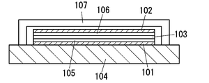
- an organic electroluminescence device having the configuration shown in FIG. 9 has been proposed (Japanese Patent Application Publication No. 2006-331694 (hereinafter referred to as “Document 1”)).
- the organic electroluminescence element of this document 1 one electrode (cathode) 101 is laminated on the surface of a substrate 104, and a light emitting layer 103 is laminated on the surface of the electrode 101 via an electron injection / transport layer 105, thereby producing a light emitting layer.
- the other electrode (anode) 102 is laminated on 103 via a hole injection / transport layer 106.
- the organic electroluminescence element includes a sealing member 107 on the surface side of the substrate 104. Therefore, in this organic electroluminescence element, light emitted from the light emitting layer 103 is radiated through the electrode 102 formed as a light transmissive electrode and the sealing member 107 formed of a transparent body.
- Examples of the material of the reflective electrode 101 include Al, Zr, Ti, Y, Sc, Ag, and In.
- Examples of the material of the electrode 102 which is a light transmissive electrode include indium-tin oxide (ITO) and indium-zinc oxide (IZO).
- the organic electroluminescence element In order to light the organic electroluminescence element with high brightness, it is necessary to pass a larger current.
- the organic electroluminescence element generally has a higher sheet resistance of an anode made of an ITO film than that of a cathode made of a metal film, an alloy film, a metal compound film, etc., the potential gradient at the anode is high. As a result, the in-plane variation in luminance increases.
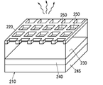
- the document 2 includes a first conductive layer 220, an electroluminescent material 230, a second conductive layer 240, and a substrate 245, and the first conductive layer 220 has a rectangular opening.
- An electroluminescent lamp 210 comprising a rectangular grid electrode having 250 has been proposed.
- Document 2 describes that it is preferable to form the first conductive layer 220 and the second conductive layer 240 with conductive ink such as silver ink or carbon ink.
- Patent Document 2 describes that the first conductive layer 220, the electroluminescent material 230, and the second conductive layer 240 are formed by a screen printing method, an offset printing method, or the like.
- Document 2 describes that when the electroluminescence lamp 210 with uniform brightness is required, the density of the openings 250 is made substantially constant over the lamp surface.
- the carrier injection property from the first conductive layer 220 to the electroluminescent material 230 is improved. Decreases, and the external quantum efficiency decreases.
- the present invention has been made in view of the above-mentioned reasons, and an object thereof is to provide an organic electroluminescence device capable of reducing luminance unevenness and improving carrier injectability. It is in.
- the present invention includes a substrate (10), a first electrode (20) provided on one surface (101) side of the substrate (10), and the first surface (101) side of the substrate (10).
- a second electrode (40) facing one electrode (20), and a functional layer (30) between the first electrode (20) and the second electrode (40) and including at least a light emitting layer (32); It is an organic electroluminescent element provided with.
- the resistivity of each of the first electrode (20) and the second electrode (40) is lower than the resistivity of the transparent conductive oxide.
- the second electrode (40) includes an opening (41) for extracting light from the functional layer (30).
- An organic electroluminescent element is equipped with the electroconductive layer (50) which has a light transmittance in the said opening part (41).
- the conductive layer (50) is in contact with the second electrode (40) and the functional layer (30).
- the organic electroluminescence element includes an insulating layer (21).
- the insulating layer (21) is provided on the surface of the first electrode (20) on the light emitting layer (30) side, faces the second electrode (40), and does not face the opening (41). It is provided in the place.
- the conductive layer (50) covers the second electrode (40).
- the height of the conductive layer (50) in the opening (41) is lower than the height (H1) of the second electrode (40).
- the functional layer (30) includes a conductive polymer layer (35) as an outermost layer in contact with both the second electrode (40) and the conductive layer (50).
- the second electrode (40) is an anode
- the functional layer (30) includes a hole injection layer located closer to the second electrode (40) than the light emitting layer (32). .
- the second electrode (40) is an anode
- the conductive layer (50) has a hole injection function
- the functional layer (30) includes the second electrode (40) and the conductive layer.
- An electron blocking layer (33) that suppresses leakage of electrons from the light emitting layer (32) side is included as the outermost layer in contact with both of the layers (50).
- the second electrode (40) is an anode
- the conductive layer (50) has a hole injection function
- the functional layer (30) includes the second electrode (40) and the conductive layer.
- a conductive polymer layer (35) having a hole injection function is included as the outermost layer in contact with both layers (50).
- the second electrode (40) is composed of an electrode containing a metal powder and an organic binder.
- the conductive layer (50) is made of a transparent conductive film including a conductive nanostructure and a transparent medium, or a metal thin film having a thickness capable of transmitting light from the functional layer (30). .
- the insulating layer (21) is formed by oxidizing the first electrode (20).
- the organic electroluminescence device In the organic electroluminescence device according to the present invention, it is possible to reduce the luminance unevenness and improve the carrier injection property.
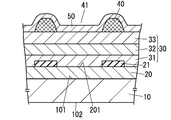
- FIG. 1 is a schematic cross-sectional view of an organic electroluminescence element of Embodiment 1.
- FIG. 3 is a schematic plan view of a second electrode in the organic electroluminescence element of Embodiment 1.
- FIG. 2 is a schematic cross-sectional view of a main part of the organic electroluminescence element of Embodiment 1.
- FIG. 6 is a schematic plan view of another configuration example of the second electrode in the organic electroluminescence element of Embodiment 1.
- FIG. 6 is a schematic plan view of another configuration example of the second electrode in the organic electroluminescence element of Embodiment 1.
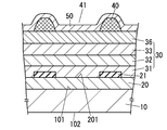
- FIG. 5 is a schematic cross-sectional view of a main part of an organic electroluminescence element of Embodiment 2.
- FIG. 6 is a schematic cross-sectional view of a main part of an organic electroluminescence element of Embodiment 3.
- FIG. 6 is a schematic cross-sectional view of a main part of an organic electroluminescence element of Embodiment 4.
- FIG. It is a schematic sectional drawing of the organic electroluminescent element of a prior art example. It is the transparent upper surface and sectional drawing of the electroluminescent lamp of a prior art example.
- the organic electroluminescence element includes a substrate 10, a first electrode 20 provided on one surface of the substrate 10 (upper surface 101 of the substrate 10 in the example of FIG. 1), and a first electrode 20 on the upper surface 101 side of the substrate 10.
- the second electrode 40 facing each other and the functional layer 30 including at least the light emitting layer 32 between the first electrode 20 and the second electrode 40 are provided.
- the substrate 10 has a first surface (upper surface) 101 and a second surface (lower surface) 102, the first electrode 20 faces the second electrode 40, and the first electrode 20 is connected to the substrate 10. It is formed on the first surface 101 of the substrate 10 so as to be disposed between the second electrode 40.
- the organic electroluminescence element has a first terminal portion (not shown) electrically connected to the first electrode 20 via a first lead wiring (not shown), and a second lead to the second electrode 40. And a second terminal portion 47 electrically connected via the wiring 46.
- the first lead wiring, the first terminal portion, the second lead wiring 46 and the second terminal portion 47 are provided on the first surface 101 side of the substrate 10.
- the second lead wiring 46 is electrically connected to a part of the functional layer 30 (side surface in the example of FIG. 1), the first electrode 20, and the first lead wiring continuous with the first electrode 20.
- An insulating film 60 is provided on the side surface of the functional unit 30 and the first surface 101 side of the substrate 10. More specifically, the insulating film 60 includes the first surface 101 of the substrate 10, the side surface of the first electrode 20, the side surface of the functional layer 30, and the outer peripheral portion of the surface of the functional layer 30 on the second electrode 40 side. It is formed across.
- each of the first electrode 20 and the second electrode 40 is formed so as to have a resistivity lower than that of a transparent conductive oxide (TCO).
- TCO transparent conductive oxide
- the transparent conductive oxide include ITO, AZO, GZO, and IZO.
- the resistivity of such a transparent conductive oxide is not particularly limited, but is exemplified as 1 ⁇ 10 ⁇ 4 to 1 ⁇ 10 ⁇ 3 ⁇ ⁇ cm.
- the second electrode 40 of the organic electroluminescence element has an opening 41 (see FIGS. 2 to 8) for extracting light from the functional layer 30.
- the organic electroluminescence element at least the opening 41 is provided with a light-transmitting conductive layer 50 and is in contact with the second electrode 40 and the functional layer 30. Thereby, the organic electroluminescence element can extract light from the second electrode 40 side.
- the organic electroluminescence element of the present embodiment can be used as a top emission type organic electroluminescence element.
- the organic electroluminescence element is disposed opposite to the first surface 101 side of the substrate 10 and has a light-transmitting cover substrate 70, and a frame shape (a book) interposed between the peripheral portion of the substrate 10 and the peripheral portion of the cover substrate 70.
- a frame portion 80 having a rectangular frame shape.
- the organic electroluminescence element includes the element portion 1 including the first electrode 20, the functional layer 30, the second electrode 40, the conductive layer 50, and the like in a space surrounded by the substrate 10, the cover substrate 70, and the frame portion 80.
- a sealing portion 90 made of a light-transmitting material (for example, a light-transmitting resin) to be sealed.
- each component of the organic electroluminescence element will be described in detail. 1 to 8, each component is different from the actual size.
- the substrate 10 has a rectangular shape in plan view.
- the planar view shape of the substrate 10 is not limited to a rectangular shape, and may be, for example, a polygonal shape or a circular shape other than the rectangular shape.
- the glass substrate is used as the substrate 10, but is not limited thereto, and for example, a plastic plate or a metal plate may be used.
- a material for the glass substrate for example, soda lime glass, non-alkali glass, or the like can be employed.
- a material of the plastic plate for example, polyethylene terephthalate, polyethylene naphthalate, polyethersulfone, polycarbonate, or the like can be employed.
- a material of the metal plate for example, aluminum, copper, stainless steel, or the like can be employed.
- the substrate 10 may be rigid or flexible.
- the unevenness of the first surface 101 of the substrate 10 may cause a leakage current of the organic electroluminescence element. That is, it is considered that the occurrence of this leakage current or the like causes deterioration of the organic electroluminescence element. For this reason, when a glass substrate is used as the substrate 10, it is preferable to prepare a glass substrate for element formation that is polished with high accuracy so that the surface roughness of the first surface 101 becomes small.
- the arithmetic average roughness Ra specified by JIS B 0601-2001 (ISO 4287-1997) is 10 nm or less.
- an arithmetic average roughness Ra of the first surface 101 of several nanometers or less can be obtained at a low cost without performing highly accurate polishing. Is possible.
- the glass substrate is used as the cover substrate 70, but is not limited thereto, and for example, a plastic plate or the like may be used.
- a material for the glass substrate for example, soda lime glass, non-alkali glass, or the like can be employed.
- a material of the plastic plate for example, polyethylene terephthalate, polyethylene naphthalate, polyethersulfone, polycarbonate, or the like can be employed.
- a flat substrate is used as the cover substrate 70, but is not limited to this, and a substrate in which a storage recess for storing the above-described element unit 1 is formed on the surface facing the substrate 10 is used.
- the peripheral portion of the storage recess on the facing surface may be joined to the first surface 101 side of the substrate 10 over the entire circumference. In this case, there is an advantage that it is not necessary to use the frame part 80 which is a separate member.
- a light extraction structure (not shown) that suppresses reflection of light emitted from the light emitting layer 32 on the outer surface 701.
- a light extraction structure part include an uneven structure part having a two-dimensional periodic structure.
- the period of such a two-dimensional periodic structure is such that when the wavelength of light emitted from the light emitting layer 32 is in the range of 300 to 800 nm, for example, the wavelength in the medium is ⁇ (the wavelength in vacuum is divided by the refractive index of the medium). Value), it is desirable to set appropriately within the range of 1/4 to 10 times the wavelength ⁇ .
- Such an uneven structure portion is formed in advance on the outer surface 701 side of the cover substrate 70 by, for example, an imprint method such as a thermal imprint method (thermal nanoimprint method) or an optical imprint method (photo nanoimprint method). It is possible. Further, depending on the material of the cover substrate 70, the cover substrate 70 may be formed by injection molding, and the uneven structure portion may be directly formed on the cover substrate 70 by using an appropriate mold at the time of injection molding. Further, the concavo-convex structure portion can also be configured by a member different from the cover substrate 70, for example, a prism sheet (for example, a light diffusion film such as Lightup (registered trademark) GM3 manufactured by Kimoto Co., Ltd.). Can be configured.
- an imprint method such as a thermal imprint method (thermal nanoimprint method) or an optical imprint method (photo nanoimprint method). It is possible.
- the cover substrate 70 may be formed by injection molding, and the uneven structure portion may be directly formed on the cover substrate 70 by using an appropriate mold
- the organic electroluminescence element of this embodiment by providing the above-described light extraction structure portion, it is possible to reduce the reflection loss of the light emitted from the light emitting layer 32 and reaching the outer surface 701 side of the cover substrate 70, and to improve the light extraction efficiency. Can be achieved.
- the frame unit 80 and the first surface 101 side of the substrate 10 are bonded by a first bonding material.
- a first bonding material an epoxy resin is used.
- the first bonding material is not limited thereto, and for example, an acrylic resin may be used.
- an epoxy resin or an acrylic resin exemplified as the first bonding material can be cured by, for example, ultraviolet rays or heat.
- an epoxy resin containing a filler for example, silica, alumina, etc.
- the frame portion 80 is airtightly bonded to the first surface 101 side of the substrate 10 over the entire circumference of the surface of the frame portion 80 facing the substrate 10 side.
- the frame portion 80 and the cover substrate 70 are bonded by the second bonding material.
- an epoxy resin is used as the second bonding material.
- an epoxy resin or an acrylic resin exemplified as the second bonding material can be cured by, for example, ultraviolet rays or heat.
- an epoxy resin containing a filler for example, silica, alumina, etc.
- the frame portion 80 is airtightly bonded to the cover substrate 70 over the entire circumference of the surface of the frame portion 80 facing the cover substrate 70.
- polyimide resin As a material of the insulating film 60, for example, polyimide resin, novolac resin, epoxy resin, or the like can be used.
- the translucent material that is a material of the sealing portion 90
- a translucent resin such as an epoxy resin or a silicone resin
- the light transmissive material may contain a light diffusing material made of glass or the like in a light transmissive resin.
- an organic / inorganic hybrid material prepared by mixing and bonding an organic component and an inorganic component at the nm (nanometer) level or molecular level may be used.
- the first electrode 20 constitutes a cathode and the second electrode 40 constitutes an anode, but an insulating layer 21 is provided on the upper surface 201 of the first electrode 20. Further, the insulating layer 21 is provided at a location facing the second electrode 40 and not facing the opening 41 (location where the second electrode 40 is projected onto the first electrode 20). That is, the planar view shapes of the second electrode 40 and the insulating layer 21 are substantially the same.
- Such an insulating layer 21 can be formed, for example, by oxidizing the above-mentioned portion of the first electrode 20.
- the insulating layer 21 can also be formed at the above-mentioned location of the first electrode 20 by printing a resin solution such as polyimide resin, novolak resin, or epoxy resin by a screen printing method or the like.
- the insulating layer 21 thus formed has a higher resistivity than the first electrode 20 and does not function as the first electrode 20.
- the functional layer 30 includes a first carrier injection layer 31, a light emitting layer 32, an interlayer 33, and a second carrier injection layer 34 in this order from the first electrode 20 side.
- the first carrier injected from the first electrode 20 into the functional layer 30 is an electron
- the second carrier injected from the second electrode 40 into the functional layer 30 is a hole.
- the first carrier injection layer 31 is an electron injection layer
- the second carrier injection layer 34 is a hole injection layer.
- the insulating layer 21 does not function as the first electrode 20
- electrons serving as the first carriers are located on the surface of the first electrode 20 on the light emitting layer 32 side where the insulating layer 21 is not provided (that is, the second electrode
- the functional layer 30 is injected from a portion that does not face 40 and faces the opening 41.
- a hole injection layer is used as the first carrier injection layer 31 and an electron injection layer is used as the second carrier injection layer 34.
- a hole blocking layer may be provided as the outermost layer of the functional layer 30 instead of the electron blocking layer described later.
- the insulating layer 21 may be provided on the surface of the first electrode 20 on the light emitting layer 32 side as described above.
- the structure of the functional layer 30 described above is not limited to the example of FIG. 1.
- an electron transport layer is provided as a first carrier transport layer between the first carrier injection layer 31 and the light emitting layer 32, or second carrier injection is performed.
- a structure in which a hole transport layer is provided as a second carrier transport layer between the layer 34 and the interlayer 33 may be used.
- the functional layer 30 only needs to include at least the light emitting layer 32 (that is, the functional layer 30 may be only the light emitting layer 32), and the first carrier injection layer 31 and the first carrier transport other than the light emitting layer 32 may be used.
- the layer, the interlayer 33, the second carrier transport layer, the second carrier injection layer 34, and the like may be provided as appropriate.
- the light emitting layer 32 may have a single layer structure or a multilayer structure.
- the emission layer may be doped with three types of dopant dyes of red, green, and blue, or the blue hole-transporting emission layer and the green electron-transporting property.
- a laminated structure of a light emitting layer and a red electron transporting light emitting layer may be adopted, or a laminated structure of a blue electron transporting light emitting layer, a green electron transporting light emitting layer and a red electron transporting light emitting layer may be adopted. Good.
- Examples of the material of the light emitting layer 32 include polyparaphenylene vinylene derivatives, polythiophene derivatives, polyparaphenylene derivatives, polysilane derivatives, polyacetylene derivatives, and the like, polyfluorene derivatives, polyvinylcarbazole derivatives, dye bodies, and metal complex light emitting materials.
- the light emitting layer 32 is preferably formed by a wet process such as a coating method (for example, spin coating method, spray coating method, die coating method, gravure printing method, screen printing method, etc.).
- a coating method for example, spin coating method, spray coating method, die coating method, gravure printing method, screen printing method, etc.
- the method for forming the light emitting layer 32 is not limited to the coating method, and the light emitting layer 32 may be formed by a dry process such as a vacuum deposition method or a transfer method.
- the material for the electron injection layer examples include metal fluorides such as lithium fluoride and magnesium fluoride, metal halides such as sodium chloride and magnesium chloride, titanium, zinc, magnesium, calcium, An oxide such as barium or strontium can be used.
- the electron injection layer can be formed by a vacuum deposition method.
- an organic semiconductor material mixed with a dopant (such as an alkali metal) that promotes electron injection can be used.
- the electron injection layer can be formed by a coating method.
- the material for the electron transport layer can be selected from the group of compounds having electron transport properties.
- this type of compound include metal complexes known as electron transport materials such as Alq 3 and compounds having a heterocycle such as phenanthroline derivatives, pyridine derivatives, tetrazine derivatives, oxadiazole derivatives, etc. Instead, any generally known electron transport material can be used.
- a low molecular material or a polymer material having a low LUMO (Lowest Unoccupied Molecular Molecular) level can be used.
- examples thereof include polymers containing aromatic amines such as polyvinyl carbazole (PVCz), polyarylene derivatives such as polypyridine and polyaniline, and polyarylene derivatives having aromatic amines in the main chain, but are not limited thereto.
- Examples of the material for the hole transport layer include 4,4′-bis [N- (naphthyl) -N-phenyl-amino] biphenyl ( ⁇ -NPD) and N, N′-bis (3-methylphenyl).
- TPD -(1,1'-biphenyl) -4,4'-diamine
- 2-TNATA 4,4 ', 4 "-tris (N- (3-methylphenyl) N-phenylamino) triphenylamine (MTDATA), 4,4′-N, N′-dicarbazole biphenyl (CBP), spiro-NPD, spiro-TPD, spiro-TAD, TNB, and the like can be used.
- Examples of the material for the hole injection layer include organic materials including thiophene, triphenylmethane, hydrazoline, amiramine, hydrazone, stilbene, triphenylamine, and the like.
- organic materials including thiophene, triphenylmethane, hydrazoline, amiramine, hydrazone, stilbene, triphenylamine, and the like.
- PET polystyrene sulfonate
- aromatic amine derivatives such as TPD, etc.
- Such a hole injection layer can be formed by a wet process such as a coating method (spin coating method, spray coating method, die coating method, gravure printing method, etc.).
- the interlayer 33 has a carrier blocking function (here, an electron barrier) that suppresses leakage of first carriers (here, electrons) from the light emitting layer 32 side to the second electrode 40 side. Then, it is preferable to have an electronic blocking function. Furthermore, the interlayer 33 preferably has a function of transporting second carriers (here, holes) to the light emitting layer 32, a function of suppressing quenching of the excited state of the light emitting layer 32, and the like. In the present embodiment, the interlayer 33 constitutes an electron blocking layer that suppresses leakage of electrons from the light emitting layer 32 side.
- a carrier blocking function here, an electron barrier
- interlayer 33 In the organic electroluminescence element, by providing the interlayer 33, it becomes possible to improve the luminous efficiency and extend the life.
- the material of the interlayer 33 for example, polyarylamine or a derivative thereof, polyfluorene or a derivative thereof, polyvinylcarbazole or a derivative thereof, a triphenyldiamine derivative, or the like can be used.
- Such an interlayer 33 can be formed by a wet process such as a coating method (spin coating method, spray coating method, die coating method, gravure printing method, etc.).
- the first electrode 20 When the first electrode 20 is a cathode, electrons (first carriers) that are first charges are injected into the functional layer 30.
- the cathode material it is preferable to use an electrode material made of a metal, an alloy, an electrically conductive compound and a mixture thereof having a low work function, so that the difference from the LUMO (Lowest Unoccupied Molecular Orbital) level does not become too large. It is preferable to use a material having a work function of 1.9 eV or more and 5 eV or less.
- the electrode material for the cathode examples include aluminum, silver, magnesium, gold, copper, chromium, molybdenum, palladium, tin, and alloys of these with other metals, such as magnesium-silver mixture, magnesium-indium mixture, aluminum -Lithium alloys can be mentioned as examples.
- it consists of a metal, a metal oxide, etc., and a mixture of these and other metals, for example, an ultra-thin film made of aluminum oxide (here, a thin film of 1 nm or less capable of flowing electrons by tunnel injection) and aluminum.
- a laminated film with a thin film can also be used.
- the cathode material is preferably a metal having a high reflectance with respect to light emitted from the light emitting layer 32 and a low resistivity, and preferably aluminum or silver.
- the material of the first electrode 20 is a work function It is preferable to use a large metal, and it is preferable to use a metal having a work function of 4 eV or more and 6 eV or less so that the difference from the HOMO (Highest Occupied Molecular Orbital) level does not become too large.
- the second electrode 40 is made of an electrode containing metal powder and an organic binder.
- this type of metal for example, silver, gold, copper or the like can be employed.
- the second electrode 40 of the organic electroluminescence element can reduce the resistivity and sheet resistance of the second electrode 40 as compared with the case of a thin film formed of a conductive transparent oxide. By reducing the resistance of the electrode 40, it is possible to reduce luminance unevenness.
- the conductive material of the second electrode 40 an alloy, carbon black, or the like can be used instead of a metal.
- the second electrode 40 can be formed, for example, by printing a paste (printing ink) in which an organic binder and an organic solvent are mixed with metal powder by, for example, a screen printing method or a gravure printing method.
- the organic binder include acrylic resin, polyethylene, polypropylene, polyethylene terephthalate, polymethyl methacrylate, polystyrene, polyether sulfone, polyarylate, polycarbonate resin, polyurethane, polyacrylonitrile, polyvinyl acetal, polyamide, polyimide, and diacryl phthalate resin.
- Cellulose resins Polyvinyl chloride, polyvinylidene chloride, polyvinyl acetate, other thermoplastic resins, and copolymers of two or more monomers constituting these resins, but are not limited thereto. It is not something.
- the thickness of the first electrode 20 is 80 to 200 nm
- the thickness of the first carrier injection layer 31 is 5 to 50 nm
- the thickness of the light emitting layer 32 is 60 to 100 nm
- the film thickness of the layer 33 is set to 15 nm
- the film thickness of the second carrier injection layer 34 is set to 10 to 100 nm, but these numerical values are merely examples and are not particularly limited.
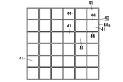
- the second electrode 40 is formed in a lattice shape (mesh shape) and has a plurality (36 in the example shown in FIG. 2) of opening portions 41.
- each opening 41 has a square shape.
- the second electrode 40 shown in FIG. 2 is formed in a square lattice shape.
- the second electrode 40 has, for example, a line width L1 (see FIG. 3) of 1 ⁇ m to 100 ⁇ m and a height H1 (see FIG. 3) regarding the dimensions of the square-lattice electrode pattern 40a constituting the second electrode 40. 50 nm to 100 ⁇ m and the pitch P 1 (see FIG. 3) may be set to 100 ⁇ m to 2000 ⁇ m. However, the numerical ranges of the line width L1, the height H1, and the pitch P1 of the electrode pattern 40a of the second electrode 40 are not particularly limited, and may be set as appropriate based on the planar size of the element portion 1.
- the line width L1 of the electrode pattern 40a of the second electrode 40 is preferably narrow from the viewpoint of the utilization efficiency of the light emitted from the light emitting layer 32, and luminance unevenness is reduced by reducing the resistance of the second electrode 40. Therefore, it is preferable that the width is appropriately set based on the planar size of the organic electroluminescence element.
- the height H1 of the second electrode 40 from the viewpoint of lowering the resistance of the second electrode 40, the use efficiency of the material of the second electrode 40 when the second electrode 40 is formed by a coating method such as a screen printing method. From the viewpoint of (material use efficiency), the viewpoint of the emission angle of light emitted from the functional layer 30, and the like, 100 nm or more and 10 ⁇ m or less are more preferable.
- each opening 41 in the second electrode 40 has an opening shape in which the opening area gradually increases as the distance from the functional layer 30 increases, as shown in FIGS. is there.
- the organic electroluminescence element can increase the spread angle of the light emitted from the functional layer 30, and can further reduce the luminance unevenness.
- the organic electroluminescence element can reduce reflection loss and absorption loss at the second electrode 40, and can further improve the external quantum efficiency.
- each of the plurality of openings 41 is not limited to a square shape, and may be, for example, a rectangular shape, a regular triangle shape, or a regular hexagonal shape.
- the second electrode 40 has a triangular lattice shape when each shape of the opening 41 is a regular triangle, and has a hexagonal lattice shape when each shape of the opening 41 is a regular hexagon.
- the second electrode 40 is not limited to a lattice shape, and may be, for example, a comb shape or may be configured by two comb-shaped electrode patterns.
- the number of the openings 41 is not particularly limited, and the number of the second electrodes 40 is not limited to a plurality, and may be one. For example, when the second electrode 40 is formed into a comb-shaped electrode pattern or formed into two comb-shaped electrode patterns, the number of openings 41 can be reduced to one.
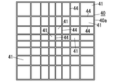
- the second electrode 40 may have a planar shape as shown in FIG. 4, for example. That is, the second electrode 40 has a constant line width of the linear thin line portion 44 in the electrode pattern 40a in plan view, and the interval between the adjacent thin line portions 44 as it approaches the central portion from the peripheral portion of the second electrode 40. It is good also as a shape which becomes narrow and the opening area of the opening part 41 becomes small.
- the second electrode 40 has a planar shape as shown in FIG. 4, so that the second terminal portion 47 in the second electrode 40 is compared with the planar shape as shown in FIG. 2. It becomes possible to improve the light emission efficiency in the central part far from the peripheral part (see FIG. 1), and to improve the external quantum efficiency.
- the organic electroluminescence element has the first terminal portion of the functional layer 30 as compared with the case where the planar shape as shown in FIG. 2 is obtained by making the planar shape of the second electrode 40 as shown in FIG.
- the organic electroluminescence element since it is possible to suppress current concentration in the peripheral portion where the distance from the second terminal portion 47 is short, it is possible to extend the life.
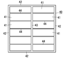
- the second electrode 40 may have a planar shape as shown in FIG. 5, for example. That is, the second electrode 40 has a line width of the four first thin wire portions 42 on the outermost periphery of the second electrode 40 in plan view, and one second thin wire portion 43 in the center in the left-right direction in FIG. The line width is set to be wider than the fine line part (third fine line part) 44 between the first fine line part 42 and the second fine line part 43.
- the second electrode 40 has a planar shape as shown in FIG. 5, so that the second terminal portion 47 (see FIG. 1) of the second electrode 40 is compared with the planar shape as shown in FIG. 2.
- the second electrode 40 has a planar shape as shown in FIG. 5, the height of the first thin wire portion 42 and the second thin wire portion 43 having a relatively wide line width is higher than the height of the third thin wire portion 44. By increasing the height, it is possible to further reduce the resistance of each of the first thin wire portion 42 and the second thin wire portion 43.
- the conductive layer 50 is preferably composed of either a transparent conductive film containing an electrical nanostructure and a transparent medium, or a metal thin film having a thickness that can transmit light from the functional layer 30.
- the conductive layer 50 has a function as a second carrier injection path from the second electrode 40 to the functional layer 30.
- the second carrier is a hole when the second electrode 40 is an anode, and an electron when the second electrode 40 is a cathode.
- the functional layer is formed from the second electrode 40. It is presumed that the injection of the second carrier into 30 is performed only through the interface between the second electrode 40 and the functional layer 30.
- the injection of the second carrier from the second electrode 40 to the functional layer 30 is performed not only at the interface between the second electrode 40 and the functional layer 30. This is performed through the interface between the second electrode 40 and the conductive layer 50 and the interface between the conductive layer 50 and the functional layer 30.
- the first carrier is an electron when the first electrode 20 is a cathode, and is a hole when the first electrode 20 is an anode.
- the insulating layer 21 when the insulating layer 21 is not provided, it is assumed that the injection of the first carrier from the first electrode 20 to the functional layer 30 is performed through the entire interface where the first electrode 20 and the functional layer 30 are in contact. Is done.
- the first carrier 20 is injected into the functional layer 30 from the first electrode 20 by the insulating layer 21 in the interface between the first electrode 20 and the functional layer 30. This is preferentially performed through a portion not provided (a portion facing the opening 41). Then, the first carrier and the second carrier can be preferentially recombined to emit light in the portion immediately below the opening 41 compared to the portion between the second electrode 40 and the insulating layer 21 in the light emitting layer 32. As a result, it is possible to improve the external quantum efficiency.
- conductive nanostructure conductive nanoparticles, conductive nanowires, or the like can be used.
- the particle diameter of the conductive nanoparticles is preferably 1 to 100 nm.
- the diameter of the conductive nanowire is preferably 1 to 100 nm.
- the material for the conductive nanostructure for example, silver, gold, ITO, IZO and the like can be employed.
- the binder that is a transparent medium include acrylic resin, polyethylene, polypropylene, polyethylene terephthalate, polymethyl methacrylate, polystyrene, polyethersulfone, polyarylate, polycarbonate resin, polyurethane, polyacrylonitrile, polyvinyl acetal, polyamide, polyimide, diethylene.
- a conductive polymer such as polythiophene, polyaniline, polypyrrole, polyphenylene, polyphenylene vinylene, polyacetylene, polycarbazole as the binder. These may be used alone or in combination.
- the conductive layer 50 can further improve conductivity by adopting a conductive polymer as a binder.
- a binder in order to improve electroconductivity, you may employ
- the conductive layer 50 is formed of a metal thin film as described above, for example, silver or gold can be employed as the material of the metal thin film.
- the thickness of this type of metal thin film may be 30 nm or less, but is preferably 20 nm or less and more preferably 10 nm or less from the viewpoint of light transmittance. However, if the thickness is too thin, the effect of improving the injection property of the second carrier to the functional layer 30 along the path from the second electrode 40 through the conductive layer 50 is reduced.
- the resistivity of each of the first electrode 20 and the second electrode 40 is lower than the resistivity of the transparent conductive oxide.
- the second electrode 40 has an opening 41 for extracting light from the functional layer 30, and the organic electroluminescence element further includes a conductive layer 50.
- the conductive layer 50 is light transmissive, is provided at least in the opening 41, and is in contact with the second electrode 40 and the functional layer 30.
- the organic electroluminescence element further includes an insulating layer 21, and the insulating layer 21 is provided at a predetermined position of the first electrode 20 (a position where the second electrode 40 is projected onto the first electrode 20). . Therefore, it is possible to reduce luminance unevenness and improve carrier (second carrier) injectability.
- the conductive layer 50 covers the second electrode 40. Thereby, in an organic electroluminescent element, it becomes possible to improve the injectability of the carrier from the 2nd electrode 40 to the functional layer 30 more.
- the height of the conductive layer 50 in the opening 41 of the second electrode 40 is preferably lower than the height H1 of the second electrode 40.
- the second electrode 40 is an anode
- the functional layer 30 includes a hole injection layer 34 on the second electrode 40 side with respect to the light emitting layer 32.
- the organic electroluminescence element of the present embodiment is substantially the same as that of the first embodiment.
- the functional layer 30 is conductive as the outermost layer where both the second electrode 40 and the conductive layer 50 are in contact.
- the difference is that the conductive polymer layer 35 is included.
- symbol is attached
- the conductive polymer layer 35 can be formed of a transparent conductive film including a conductive nanostructure and a transparent medium, like the conductive layer 50.
- the functional layer 30 includes the conductive polymer layer 35 as the outermost layer where both the second electrode 40 and the conductive layer 50 are in contact with each other, and thus flows to the light emitting layer 32. It becomes possible to further reduce the in-plane variation of the current and to further reduce the luminance unevenness.
- the organic electroluminescence element of this embodiment is substantially the same as that of Embodiment 1, and as shown in FIG. 7, the conductive layer 50 has a hole injection function, and the functional layer 30 includes the second electrode 40 and the conductive layer. 50 is different in that, for example, an interlayer 33 is included as the outermost layer in contact with both. Moreover, in the organic electroluminescent element of this embodiment, since the conductive layer 50 has a hole injection function, the second carrier injection layer 34 as the hole injection layer described in the first embodiment is not provided.
- symbol is attached
- the second electrode 40 is an anode
- the conductive layer 50 has a hole injection function
- the functional layer 30 is the most in contact with both the second electrode 40 and the conductive layer 50. Since the interlayer 33 is included as a surface layer (including an electron blocking layer that suppresses leakage of electrons from the light emitting layer 32 side), it is possible to further reduce luminance unevenness.
- the organic electroluminescence element of this embodiment is substantially the same as that of Embodiment 1, and as shown in FIG. 8, the conductive layer 50 has a hole injection function, and the functional layer 30 includes the second electrode 40 and the conductive layer. 50 is different in that, for example, a conductive polymer layer 36 having a hole injection function is included as the outermost layer in contact with both. Moreover, in the organic electroluminescent element of this embodiment, since the conductive layer 50 has a hole injection function, the second carrier injection layer 34 as the hole injection layer described in the first embodiment is not provided.
- symbol is attached
- the conductive polymer layer 36 having a hole injection function can be formed by, for example, the conductive nanostructure and the conductive polymer described in the first embodiment.
- the second electrode 40 is an anode
- the conductive layer 50 has a hole injection function
- the functional layer 30 is the most in contact with both the second electrode 40 and the conductive layer 50. Since the conductive polymer layer 36 having the hole injection function is included as the surface layer, the luminance unevenness can be further reduced.
- the organic electroluminescent elements described in Embodiments 1 to 4 can be suitably used as, for example, an organic electroluminescent element for illumination, but can be used not only for illumination but also for other applications.
Abstract
本発明は、基板と、前記基板に設けられた第1電極と、前記第1電極に対向した第2電極と、前記第1電極と前記第2電極との間にありかつ発光層を含む機能層とを備えた有機エレクトロルミネッセンス素子である。前記第1電極及び前記第2電極の各抵抗率が透明導電性酸化物の抵抗率よりも低くい。前記第2電極が、前記機能層からの光の取り出し用の開口部を備える。有機エレクトロルミネッセンス素子は、前記開口部に光透過性を有する導電性層を備える。この導電性層は、前記第2電極と前記機能層とに接する。有機エレクトロルミネッセンス素子は、絶縁層を備える。この絶縁層は、前記第1電極の発光層側の面に設けられ、かつ前記第2電極と対向し、かつ前記開口部と対向しない箇所に設けられる。
Description
本発明は、有機エレクトロルミネッセンス素子に関するものである。
従来から、図9に示す構成の有機エレクトロルミネッセンス素子が提案されている(日本国特許出願公開番号2006-331694(以下、「文献1」という))。この文献1の有機エレクトロルミネッセンス素子は、一方の電極(陰極)101が基板104の表面に積層され、電極101の表面上に電子注入・輸送層105を介して発光層103が積層され、発光層103上に、ホール注入・輸送層106を介して他方の電極(陽極)102が積層されている。また、この有機エレクトロルミネッセンス素子は、基板104の上記表面側に封止部材107を備えている。したがって、この有機エレクトロルミネッセンス素子では、発光層103で発光した光が、光透過性電極として形成される電極102、透明体で形成される封止部材107を通して放射されるようになっている。
反射性の電極101の材料としては、例えば、Al、Zr、Ti、Y、Sc、Ag、Inなどが挙げられている。また、光透過性電極である電極102の材料としては、例えば、インジウム-錫酸化物(ITO)、インジウム-亜鉛酸化物(IZO)などが挙げられている。
ところで、有機エレクトロルミネッセンス素子を高輝度で点灯させるためには、より大きな電流を流す必要がある。しかしながら、有機エレクトロルミネッセンス素子は、一般的に、ITO膜からなる陽極のシート抵抗が、金属膜、合金膜、金属化合物膜などからなる陰極のシート抵抗に比べて高いため、陽極での電位勾配が大きくなって、輝度の面内ばらつきが大きくなってしまう。
また、従来から、スパッタ法により形成されるITO膜からなる電極を備えた構成の問題点を解決するエレクトロルミネセンス・ランプとして、ITO膜からなる電極を用いずに構成されたエレクトロルミネセンス・ランプが提案されている(日本国特許出願公開番号2002-502540(以下、「文献2」という))。文献2には、例えば、図10に示すように、第1の導電層220、エレクトロルミネセンス物質230、第2の導電層240及び基板245を備え、第1の導電層220が、矩形の開口250を有する矩形格子電極により構成されてなるエレクトロルミネセンス・ランプ210が提案されている。
ここで、文献2には、第1の導電層220及び第2の導電層240を、銀インク、炭素インクなどの導電性インクで形成することが好ましい旨が記載されている。また、特許文献2には、第1の導電層220、エレクトロルミネセンス物質230、第2の導電層240を、スクリーン印刷法やオフセット印刷法などにより形成することが記載されている。
なお、文献2には、均一な明るさのエレクトロルミネセンス・ランプ210が必要な場合は、ランプ表面にわたって開口250の密度を略一定とすることが記載されている。
ところで、図10に示した構成のエレクトロルミネセンス・ランプ210では、第1の導電層220が開口250を有しているので、第1の導電層220からエレクトロルミネセンス物質230へのキャリア注入性が低下してしまい、外部量子効率が低下してしまう。
本発明は上記事由に鑑みて為されたものであり、その目的は、輝度むらの低減を図ることが可能で、かつキャリアの注入性を向上させることが可能な有機エレクトロルミネッセンス素子を提供することにある。
本発明は、基板(10)と、前記基板(10)の一表面(101)側に設けられた第1電極(20)と、前記基板(10)の前記一表面(101)側で前記第1電極(20)に対向した第2電極(40)と、前記第1電極(20)と前記第2電極(40)との間にあり少なくとも発光層(32)を含む機能層(30)とを備えた有機エレクトロルミネッセンス素子である。前記第1電極(20)及び前記第2電極(40)それぞれの抵抗率が透明導電性酸化物の抵抗率よりも低くい。前記第2電極(40)が、前記機能層(30)からの光の取り出し用の開口部(41)を備える。有機エレクトロルミネッセンス素子は、前記開口部(41)に、光透過性を有する導電性層(50)を備える。この導電性層(50)は、前記第2電極(40)と前記機能層(30)とに接する。有機エレクトロルミネッセンス素子は、絶縁層(21)を備える。この絶縁層(21)は、前記第1電極(20)の発光層(30)側の面に設けられ、かつ前記第2電極(40)と対向し、かつ前記開口部(41)と対向しない箇所に設けられる。
一実施形態において、前記導電性層(50)が、前記第2電極(40)を覆っている。
一実施形態において、前記開口部(41)における前記導電性層(50)の高さは、前記第2電極(40)の高さ(H1)よりも低い。
一実施形態において、前記機能層(30)は、前記第2電極(40)と前記導電性層(50)との両方が接する最表層として、導電性高分子層(35)を含んでいる。
一実施形態において、前記第2電極(40)が陽極であり、前記機能層(30)は、前記発光層(32)よりも前記第2電極(40)側にあるホール注入層を含んでいる。
一実施形態において、前記第2電極(40)が陽極であり、前記導電性層(50)がホール注入機能を備え、前記機能層(30)は、前記第2電極(40)と前記導電性層(50)との両方が接する最表層として、前記発光層(32)側からの電子の漏れを抑制する電子ブロッキング層(33)を含んでいる。
一実施形態において、前記第2電極(40)が陽極であり、前記導電性層(50)がホール注入機能を備え、前記機能層(30)は、前記第2電極(40)と前記導電性層(50)との両方が接する最表層として、ホール注入機能を備えた導電性高分子層(35)を含んでいる。
一実施形態において、前記第2電極(40)は、金属の粉末と有機バインダとを含む電極からなる。
一実施形態において、前記導電性層(50)は、導電性ナノ構造体と透明媒体とを含む透明導電膜、あるいは、前記機能層(30)からの光を透過可能な厚みの金属薄膜からなる。
一実施形態において、前記絶縁層(21)は、前記第1電極(20)を酸化して形成される。
本発明に係る有機エレクトロルミネッセンス素子においては、輝度むらの低減を図ることが可能で、かつキャリアの注入性を向上させることが可能となる。
(実施形態1)
以下、本実施形態の有機エレクトロルミネッセンス素子について図1~図3に基づいて説明する。
以下、本実施形態の有機エレクトロルミネッセンス素子について図1~図3に基づいて説明する。
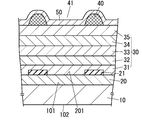
有機エレクトロルミネッセンス素子は、基板10と、基板10の一表面(図1の例では基板10の上面101)側に設けられた第1電極20と、基板10の上面101側で第1電極20に対向した第2電極40と、第1電極20と第2電極40との間にあり少なくとも発光層32を含む機能層30とを備えている。
図1の例では、基板10は第1表面(上面)101及び第2表面(下面)102を有し、第1電極20は、第2電極40と対向し、第1電極20が基板10と第2電極40との間に配置されるように、基板10の第1表面101に形成されている。
また、有機エレクトロルミネッセンス素子は、第1電極20に第1引出し配線(図示せず)を介して電気的に接続された第1端子部(図示せず)と、第2電極40に第2引出し配線46を介して電気的に接続された第2端子部47とを備えている。第1引出し配線、第1端子部、第2引出し配線46及び第2端子部47は、基板10の第1表面101側に設けられている。また、有機エレクトロルミネッセンス素子には、第2引出し配線46を、機能層30の一部(図1の例では側面)、第1電極20、及び第1電極20と連続する第1引出し配線から電気的に絶縁するための絶縁膜60が、機能部30の側面及び基板10の第1表面101側に設けられている。更に詳しく記すと、この絶縁膜60は、基板10の第1表面101と、第1電極20の側面と、機能層30の側面と、機能層30における第2電極40側の表面の外周部とに跨って形成されている。
また、有機エレクトロルミネッセンス素子では、第1電極20及び第2電極40それぞれは、透明導電性酸化物(Transparent Conducting Oxide:TCO)の抵抗率よりも低くなるように形成されている。透明導電性酸化物としては、例えば、ITO、AZO、GZO、IZOなどがある。このような透明導電酸化物の抵抗率は、特に限定されないが、1×10⁻⁴~1×10⁻³Ω・cmとして例示される。
また、有機エレクトロルミネッセンス素子の第2電極40は、機能層30からの光の取り出し用の開口部41(図2~図8参照)を有している。
また、有機エレクトロルミネッセンス素子は、少なくとも開口部41に光透過性を有する導電性層50が設けられ、かつ第2電極40と機能層30とに接している。これにより、有機エレクトロルミネッセンス素子は、第2電極40側から光を取り出すことが可能となる。要するに、本実施形態の有機エレクトロルミネッセンス素子は、トップエミッション型の有機エレクトロルミネッセンス素子として用いることが可能となる。
有機エレクトロルミネッセンス素子は、基板10の第1表面101側に対向配置され透光性を有するカバー基板70と、基板10の周部とカバー基板70の周部との間に介在する枠状(本実施形態では、矩形枠状)のフレーム部80とを備えていることが好ましい。また、有機エレクトロルミネッセンス素子は、基板10とカバー基板70とフレーム部80とで囲まれる空間に、第1電極20、機能層30、第2電極40、導電性層50などからなる素子部1を封止する透光性材料(例えば、透光性樹脂など)からなる封止部90を備えていることが好ましい。
以下、有機エレクトロルミネッセンス素子の各構成要素について詳細に説明する。なお、図1~図8において各構成要素は実際の寸法とは異なる。
基板10は、平面視形状を矩形状としてある。ここで、基板10の平面視形状は、矩形状に限らず、例えば、矩形状以外の多角形状、円形状などでもよい。
基板10としては、ガラス基板を用いているが、これに限らず、例えば、プラスチック板や、金属板などを用いてもよい。ガラス基板の材料としては、例えば、ソーダライムガラス、無アルカリガラスなどを採用することができる。また、プラスチック板の材料としては、例えば、ポリエチレンテレフタラート、ポリエチレンナフタレート、ポリエーテルサルフォン、ポリカーボネートなどを採用することができる。また、金属板の材料としては、例えば、アルミニウム、銅、ステンレス鋼などを採用することができる。プラスチック板を用いる場合は、プラスチック基板の表面にSiON膜、SiN膜などが成膜されたものを用いることで、水分の透過を抑えることが好ましい。なお、基板10は、リジッドなものでもよいし、フレキシブルなものでもよい。
基板10としてガラス基板を用いる場合には、基板10の第1表面101の凹凸が有機エレクトロルミネッセンス素子のリーク電流などの発生原因となることがある。つまり、このリーク電流などの発生が、有機エレクトロルミネッセンス素子の劣化原因となると考えられる。このため、基板10としてガラス基板を用いる場合には、第1表面101の表面粗さが小さくなるように高精度に研磨された素子形成用のガラス基板を用意することが好ましい。基板10の第1表面101(第1電極20などと接する面)の表面粗さについては、JIS B 0601-2001(ISO 4287-1997)で規定されている算術平均粗さRaが10nm以下であることが好ましく、数nm以下であることが、より好ましい。これに対して、基板10としてプラスチック板を用いる場合には、特に高精度な研磨を行わなくても、第1表面101の算術平均粗さRaが数nm以下のものを低コストで得ることが可能である。
カバー基板70としては、ガラス基板を用いているが、これに限らず、例えば、プラスチック板などを用いてもよい。ガラス基板の材料としては、例えば、ソーダライムガラス、無アルカリガラスなどを採用することができる。また、プラスチック板の材料としては、例えば、ポリエチレンテレフタラート、ポリエチレンナフタレート、ポリエーテルサルフォン、ポリカーボネートなどを採用することができる。
本実施形態では、カバー基板70として、平板状のものを用いているが、これに限らず、基板10との対向面に、上述の素子部1を収納する収納凹所を形成したものを用い、上記対向面における収納凹所の周部を全周に亘って基板10の第1表面101側と接合するようにしてもよい。この場合は、別部材のフレーム部80を用いる必要がなくなるという利点がある。一方、平板状のカバー基板70と枠状のフレーム部80とを別部材により構成している場合には、カバー基板70に要求される光学的な物性(光透過率、屈折率など)と、フレーム部80に要求される物性(ガスバリア性など)との両方の要求を各別に満たす材料を採用することが可能になるという利点がある。
カバー基板70における外面701側(基板10側とは反対の面側)には、発光層32から放射された光の外面701での反射を抑制する光取出し構造部(図示せず)を備えていることが好ましい。このような光取出し構造部としては、例えば、2次元周期構造を有した凹凸構造部が挙げられる。このような2次元周期構造の周期は、発光層32で発光する光の波長が例えば300~800nmの範囲内にある場合、媒質内の波長をλ(真空中の波長を媒質の屈折率で除した値)とすれば、波長λの1/4~10倍の範囲で適宜設定することが望ましい。このような凹凸構造部は、例えば、カバー基板70の外面701側に、例えば、熱インプリント法(熱ナノインプリント法)、光インプリント法(光ナノインプリント法)などのインプリント法により、予め形成することが可能である。また、カバー基板70の材料によっては、カバー基板70を射出成形により形成するようにし、射出成形時に適宜の金型を用いて、カバー基板70に凹凸構造部を直接形成することも可能である。また、凹凸構造部は、カバー基板70とは別部材により構成することも可能であり、例えば、プリズムシート(例えば、株式会社きもと製のライトアップ(登録商標)GM3のような光拡散フィルムなど)により構成することができる。
本実施形態の有機エレクトロルミネッセンス素子では、上述の光取出し構造部を備えることにより、発光層32から放射されカバー基板70の外面701側まで到達した光の反射ロスを低減でき、光取り出し効率の向上を図ることが可能となる。
フレーム部80と基板10の第1表面101側とは、第1接合材料により接合されている。この第1接合材料としては、エポキシ樹脂を用いているが、これに限らず、例えば、アクリル樹脂などを採用してもよい。ここで、第1接合材料として例示されるエポキシ樹脂やアクリル樹脂を、例えば、紫外線や熱などで硬化させることができる。このような第1接合材料として、エポキシ樹脂にフィラー(例えば、シリカ、アルミナなど)を含有させたものを用いてもよい。ここで、フレーム部80は、基板10の第1表面101側に対して、フレーム部80における基板10側との対向面を全周に亘って気密的に接合してある。また、フレーム部80とカバー基板70とは、第2接合材料により接合されている。この第2接合材料としては、エポキシ樹脂を用いているが、これに限らず、例えば、アクリル樹脂、フリットガラスなどを採用してもよい。ここで、第2接合材料として例示されるエポキシ樹脂やアクリル樹脂を、例えば、紫外線や熱などで硬化させることができる。このような第2接合材料として、エポキシ樹脂にフィラー(例えば、シリカ、アルミナなど)を含有させたものを用いてもよい。ここで、フレーム部80は、カバー基板70に対して、フレーム部80におけるカバー基板70との対向面を全周に亘って気密的に接合してある。
絶縁膜60の材料としては、例えば、ポリイミド樹脂、ノボラック樹脂、エポキシ樹脂などを用いることができる。
封止部90の材料である透光性材料としては、例えば、エポキシ樹脂やシリコーン樹脂などの透光性樹脂を用いることができるが、機能層30との屈折率差が小さい材料を用いることが、より好ましい。また、透光性材料には、透光性樹脂にガラスなどからなる光拡散材を含有させてもよい。また、透光性材料として、有機成分と無機成分とがnm(ナノメートル)レベルもしくは分子レベルで混合、結合して作製された有機・無機ハイブリッド材料を用いてもよい。
本実施形態の有機エレクトロルミネッセンス素子では、第1電極20が陰極を構成し、第2電極40が陽極を構成しているが、第1電極20上面201には絶縁層21が設けられている。更に、この絶縁層21は、第2電極40と対向し、かつ開口部41と対向しない箇所(第2電極40を第1電極20上に投影した箇所)に設けられている。つまり、第2電極40と絶縁層21との平面視形状は略同一である。このような絶縁層21は、例えば、第1電極20の上記の箇所を酸化させることによって形成することができる。また絶縁層21は、ポリイミド樹脂、ノボラック樹脂、エポキシ樹脂等の樹脂溶液をスクリーン印刷法などにより印刷して第1電極20の上記の箇所に形成することもできる。このようにして形成された絶縁層21は、その抵抗率が第1電極20の抵抗率よりも高くなり、第1電極20としては機能しなくなる。他方、機能層30は、第1電極20側から順に、第1キャリア注入層31、発光層32、インターレイヤー33、第2キャリア注入層34を備えている。ここで、第1電極20から機能層30へ注入する第1キャリアは電子であり、第2電極40から機能層30へ注入する第2キャリアは正孔である。したがって、第1キャリア注入層31は、電子注入層であり、第2キャリア注入層34は、ホール注入層である。このとき絶縁層21は第1電極20として機能しないので、第1キャリアである電子は、第1電極20の発光層32側の面において絶縁層21が設けられていない箇所(すなわち、第2電極40と対向せず、かつ開口部41と対向する箇所)から機能層30へ注入されることになる。なお、第1電極20が陽極を構成し、第2電極40が陰極を構成する場合には、例えば、第1キャリア注入層31としてホール注入層を、第2キャリア注入層34として電子注入層を採用し、機能層30の最表層として、後述の電子ブロッキング層の代わりに、ホールブロッキング層を設ければよい。さらにこの場合も上記と同様に第1電極20の発光層32側の面において絶縁層21を設ければよい。
上述の機能層30の構造は、図1の例に限らず、例えば、第1キャリア注入層31と発光層32との間に第1キャリア輸送層として電子輸送層を設けたり、第2キャリア注入層34とインターレイヤー33との間に第2キャリア輸送層としてホール輸送層を設けたりした構造でもよい。また、機能層30は、少なくとも発光層32を含んでいればよく(つまり、機能層30は、発光層32のみでもよく)、発光層32以外の、第1キャリア注入層31、第1キャリア輸送層、インターレイヤー33、第2キャリア輸送層、第2キャリア注入層34などは適宜設ければよい。発光層32は、単層構造でも多層構造でもよい。例えば、所望の発光色が白色の場合には、発光層中に赤色、緑色、青色の3種類のドーパント色素をドーピングするようにしてもよいし、青色正孔輸送性発光層と緑色電子輸送性発光層と赤色電子輸送性発光層との積層構造を採用してもよいし、青色電子輸送性発光層と緑色電子輸送性発光層と赤色電子輸送性発光層との積層構造を採用してもよい。
発光層32の材料としては、例えば、ポリパラフェニレンビニレン誘導体、ポリチオフェン誘導体、ポリパラフェニレン誘導体、ポリシラン誘導体、ポリアセチレン誘導体など、ポリフルオレン誘導体、ポリビニルカルバゾール誘導体、色素体、金属錯体系発光材料を高分子化したものなどや、アントラセン、ナフタレン、ピレン、テトラセン、コロネン、ペリレン、フタロペリレン、ナフタロペリレン、ジフェニルブタジエン、テトラフェニルブタジエン、クマリン、オキサジアゾール、ビスベンゾキサゾリン、ビススチリル、シクロペンタジエン、キノリン金属錯体、トリス(8-ヒドロキシキノリナート)アルミニウム錯体、トリス(4-メチル-8-キノリナート)アルミニウム錯体、トリス(5-フェニル-8-キノリナート)アルミニウム錯体、アミノキノリン金属錯体、ベンゾキノリン金属錯体、トリ-(p-ターフェニル-4-イル)アミン、ピラン、キナクリドン、ルブレン、及びこれらの誘導体、あるいは、1-アリール-2,5-ジ(2-チエニル)ピロール誘導体、ジスチリルベンゼン誘導体、スチリルアリーレン誘導体、スチリルアミン誘導体、及びこれらの発光性化合物からなる基を分子の一部分に有する化合物などが挙げられる。また、上記化合物に代表される蛍光色素由来の化合物のみならず、いわゆる燐光発光材料、例えばイリジウム錯体、オスミウム錯体、白金錯体、ユーロピウム錯体などの発光材料、又はそれらを分子内に有する化合物若しくは高分子も好適に用いることができる。これらの材料は、必要に応じて、適宜選択して用いることができる。発光層32は、塗布法(例えば、スピンコート法、スプレーコート法、ダイコート法、グラビア印刷法、スクリーン印刷法など)のような湿式プロセスによって成膜することが好ましい。ただし、発光層32の成膜方法は、塗布法に限らず、例えば、真空蒸着法、転写法などの乾式プロセスによって発光層32を成膜してもよい。
電子注入層の材料は、例えば、フッ化リチウムやフッ化マグネシウムなどの金属フッ化物、塩化ナトリウム、塩化マグネシウムなどに代表される金属塩化物などの金属ハロゲン化物や、チタン、亜鉛、マグネシウム、カルシウム、バリウム、ストロンチウムなどの酸化物、などを用いることができる。これらの材料の場合、電子注入層は、真空蒸着法により形成することができる。また、電子注入層の材料は、例えば、電子注入を促進させるドーパント(アルカリ金属など)を混合した有機半導体材料を用いることができる。このような材料の場合、電子注入層は、塗布法により形成することができる。
また、電子輸送層の材料は、電子輸送性を有する化合物の群から選定することができる。この種の化合物としては、Alq3等の電子輸送性材料として知られる金属錯体や、フェナントロリン誘導体、ピリジン誘導体、テトラジン誘導体、オキサジアゾール誘導体などのヘテロ環を有する化合物などが挙げられるが、この限りではなく、一般に知られる任意の電子輸送材料を用いることが可能である。
ホール輸送層の材料としては、LUMO(Lowest Unoccupied Molecular Orbital)準位が小さい低分子材料や高分子材料を用いることができる。例えば、ポリビニルカルバゾール(PVCz)や、ポリピリジン、ポリアニリンなどの側鎖や主鎖に芳香族アミンを有するポリアリーレン誘導体などの芳香族アミンを含むポリマーなどが挙げられるが、これらに限定されるものではない。なお、ホール輸送層の材料としては、例えば、4,4’-ビス[N-(ナフチル)-N-フェニル-アミノ]ビフェニル(α-NPD)、N,N’-ビス(3-メチルフェニル)-(1,1’-ビフェニル)-4,4’-ジアミン(TPD)、2-TNATA、4,4’,4”-トリス(N-(3-メチルフェニル)N-フェニルアミノ)トリフェニルアミン(MTDATA)、4,4’-N,N’-ジカルバゾールビフェニル(CBP)、スピロ-NPD、スピロ-TPD、スピロ-TAD、TNBなどを用いることが可能である。
ホール注入層の材料としては、例えば、チオフェン、トリフェニルメタン、ヒドラゾリン、アミールアミン、ヒドラゾン、スチルベン、トリフェニルアミンなどを含む有機材料が挙げられる。具体的には、たとえば、ポリビニルカルバゾール、ポリエチレンジオキシチオフェン:ポリスチレンスルホネート(PEDOT:PSS)、TPDなどの芳香族アミン誘導体などで、これらの材料を単独で用いてもよいし、2種類以上の材料を組み合わせて用いてもよい。このようなホール注入層は、塗布法(スピンコート法、スプレーコート法、ダイコート法、グラビア印刷法など)のような湿式プロセスによって成膜することができる。
インターレイヤー33は、発光層32側からの第2電極40側への第1キャリア(ここでは、電子)の漏れを抑制する第1キャリア障壁(ここでは、電子障壁)としてのキャリアブロッキング機能(ここでは、電子ブロッキング機能)を有することが好ましい。さらにインターレイヤー33は、第2キャリア(ここでは、正孔)を発光層32へ輸送する機能、発光層32の励起状態の消光を抑制する機能などを有していることが好ましい。なお、本実施形態では、インターレイヤー33が、発光層32側からの電子の漏れを抑制する電子ブロッキング層を構成している。
有機エレクトロルミネッセンス素子では、インターレイヤー33を設けることにより、発光効率の向上及び長寿命化を図ることが可能となる。インターレイヤー33の材料としては、例えば、ポリアリールアミン若しくはその誘導体、ポリフルオレン若しくはその誘導体、ポリビニルカルバゾール若しくはその誘導体、トリフェニルジアミン誘導体などを用いることができる。このようなインターレイヤー33は、塗布法(スピンコート法、スプレーコート法、ダイコート法、グラビア印刷法など)のような湿式プロセスによって成膜することができる。
第1電極20が陰極の場合、機能層30中に第1電荷である電子(第1キャリア)を注入することとなる。陰極の材料としては、仕事関数の小さい金属、合金、電気伝導性化合物及びこれらの混合物からなる電極材料を用いることが好ましく、LUMO(Lowest Unoccupied Molecular Orbital)準位との差が大きくなりすぎないように仕事関数が1.9eV以上5eV以下のものを用いるのが好ましい。陰極の電極材料としては、例えば、アルミニウム、銀、マグネシウム、金、銅、クロム、モリブデン、パラジウム、錫など、及びこれらと他の金属との合金、例えばマグネシウム-銀混合物、マグネシウム-インジウム混合物、アルミニウム-リチウム合金を例として挙げることができる。また、金属、金属酸化物など、及びこれらと他の金属との混合物、例えば、酸化アルミニウムからなる極薄膜(ここでは、トンネル注入により電子を流すことが可能な1nm以下の薄膜)とアルミニウムからなる薄膜との積層膜なども使用可能である。陰極を反射電極とする場合、陰極の材料としては、発光層32から放射される光に対する反射率が高く、かつ抵抗率の低い金属が好ましく、アルミニウムや銀が好ましい。なお、第1電極20が、機能層30中に第2電荷であるホール(第2キャリア)を注入するための電極である陽極を構成する場合、第1電極20の材料としては、仕事関数の大きい金属を用いることが好ましく、HOMO(Highest Occupied Molecular Orbital)準位との差が大きくなりすぎないように仕事関数が4eV以上6eV以下のものを用いるのが好ましい。
第2電極40は、金属の粉末と有機バインダとを含む電極からなる。この種の金属としては、例えば、銀、金、銅などを採用することができる。これにより、有機エレクトロルミネッセンス素子の第2電極40は、導電性透明酸化物により形成された薄膜の場合に比べて、第2電極40の抵抗率及びシート抵抗を小さくすることが可能となり、第2電極40の低抵抗化により輝度むらを低減することが可能となる。なお、第2電極40の導電性材料としては、金属の代わりに、合金や、カーボンブラックなどを用いることも可能である。
第2電極40は、例えば、金属の粉末に有機バインダ及び有機溶剤を混合させたペースト(印刷インク)を、例えばスクリーン印刷法、グラビア印刷法などにより印刷して形成することができる。有機バインダとしては、例えば、アクリル樹脂、ポリエチレン、ポリプロピレン、ポリエチレンテレフタレート、ポリメチルメタクリレート、ポリスチレン、ポリエーテルスルホン、ポリアリレート、ポリカーボネート樹脂、ポリウレタン、ポリアクリルニトリル、ポリビニルアセタール、ポリアミド、ポリイミド、ジアクリルフタレート樹脂、セルロース系樹脂、ポリ塩化ビニル、ポリ塩化ビニリデン、ポリ酢酸ビニル、その他の熱可塑性樹脂や、これらの樹脂を構成する単量体の2種以上の共重合体が挙げられるが、これらに限定されるものではない。
なお、本実施形態の有機エレクトロルミネッセンス素子では、第1電極20の膜厚を80~200nm、第1キャリア注入層31の膜厚を5~50nm、発光層32の膜厚を60~100nm、インターレイヤー33の膜厚を15nm、第2キャリア注入層34の膜厚を10~100nmにそれぞれ設定してあるが、これらの数値は一例であって、特に限定するものではない。
第2電極40は、図1及び図2に示すように、格子状(網状)に形成されており、複数(図2に示した例では36個)の開口部41を有している。ここで、図2に示した第2電極40は、各開口部41の各々の形状が正方形状である。要するに、図2に示した第2電極40は、正方格子状に形成されている。
第2電極40は、第2電極40を構成している正方格子状の電極パターン40aの寸法に関して、例えば、線幅L1(図3参照)を1μm~100μm、高さH1(図3参照)を50nm~100μm、ピッチP1(図3参照)を100μm~2000μmとすればよい。ただし、第2電極40の電極パターン40aの線幅L1、高さH1及びピッチP1それぞれの数値範囲は、特に限定するものではなく、素子部1の平面サイズに基づいて適宜設定すればよい。ここにおいて、第2電極40の電極パターン40aの線幅L1については、発光層32で発光する光の利用効率の観点からは狭い方が好ましく、第2電極40の低抵抗化によって輝度むらを低減するという観点からは広い方が好ましいので、有機エレクトロルミネッセンス素子の平面サイズなどに基づいて適宜設定することが好ましい。また、第2電極40の高さH1については、第2電極40の低抵抗化の観点、第2電極40をスクリーン印刷法などの塗布法により形成する際の第2電極40の材料の使用効率(材料使用効率)の観点、機能層30から放射される光の放射角の観点などから、100nm以上10μm以下が、より好ましい。
また、本実施形態の有機エレクトロルミネッセンス素子では、第2電極40における各開口部41を、図1及び図3に示したように、機能層30から離れるにつれて開口面積が徐々に大きくなる開口形状としてある。これにより、有機エレクトロルミネッセンス素子は、機能層30から放射される光の広がり角を大きくすることが可能になり、輝度むらをより低減することが可能となる。また、有機エレクトロルミネッセンス素子は、第2電極40での反射損失や吸収損失を低減することが可能となり、外部量子効率のより一層の向上を図ることが可能となる。
第2電極40を格子状の形状とする場合、複数の開口部41の各々の形状は正方形状に限らず、例えば、長方形状や正三角形状や正六角形状の形状としてもよい。
第2電極40は、開口部41の各々の形状が正三角形状の場合、三角格子状の形状となり、開口部41の各々の形状が正六角形状の場合、六角格子状の形状となる。なお、第2電極40は、格子状の形状に限らず、例えば、櫛形状の形状でもよいし、2つの櫛形状の電極パターンにより構成してもよい。また、第2電極40は、開口部41の数も特に限定するものではなく、複数に限らず、1つでもよい。例えば、第2電極40を櫛形状の電極パターンに形成したり、2つの櫛形状の電極パターンに形成したりすると、開口部41の数を1つにすることができる。
また、第2電極40は、例えば、図4に示すような平面形状としてもよい。すなわち、第2電極40は、平面視において、電極パターン40aにおける直線状の細線部44の線幅を一定として、第2電極40における周部から中心部に近づくにつれて隣り合う細線部44間の間隔が狭くなり開口部41の開口面積が小さくなる形状としてもよい。有機エレクトロルミネッセンス素子は、第2電極40の平面形状を図4のような平面形状とすることにより、図2のような平面形状とした場合に比べて、第2電極40において第2端子部47(図1参照)からの距離が周部よりも遠い中央部での発光効率を向上させることが可能となり、外部量子効率の向上を図ることが可能となる。また、有機エレクトロルミネッセンス素子は、第2電極40の平面形状を図4のような形状とすることにより、図2のような平面形状とした場合に比べて、機能層30のうち第1端子部及び第2端子部47からの距離が近い周部での電流集中を抑制することが可能となるから、長寿命化を図ることが可能となる。
また、第2電極40は、例えば、図5に示すような平面形状としてもよい。すなわち、第2電極40は、平面視において、第2電極40における最外周にある4つの第1細線部42の線幅と、図5において左右方向の中央にある1つの第2細線部43の線幅とを、第1細線部42と第2細線部43との間にある細線部(第3細線部)44よりも幅広としてある。有機エレクトロルミネッセンス素子は、第2電極40を図5のような平面形状とすることにより、図2のような平面形状の場合に比べて、第2電極40において第2端子部47(図1参照)からの距離が周部よりも遠い中央部での発光効率を向上させることが可能となり、外部量子効率の向上を図ることが可能となる。なお、第2電極40は、図5のような平面形状とする場合、相対的に線幅の広い第1細線部42及び第2細線部43の高さを第3細線部44の高さよりも高くすることにより、第1細線部42及び第2細線部43それぞれの、より一層の低抵抗化を図ることが可能となる。
導電性層50は、電性ナノ構造体と透明媒体とを含む透明導電膜、あるいは、機能層30からの光を透過可能な厚みの金属薄膜、のいずれかにより構成することが好ましい。この導電性層50は、第2電極40から機能層30への第2キャリアの注入経路としての機能を有している。第2キャリアは、第2電極40が陽極の場合、正孔であり、第2電極40が陰極の場合、電子である。ここで、導電性層50がない場合や、導電性層50の代わりに開口部41が電気絶縁性の封止部90の一部により埋め込まれている場合には、第2電極40から機能層30への第2キャリアの注入は、第2電極40と機能層30との接している界面のみを通して行われるものと推測される。これに対して、導電性層50を設けた場合には、第2電極40から機能層30への第2キャリアの注入は、第2電極40と機能層30との接している界面だけでなく、第2電極40と導電性層50との界面及び導電性層50と機能層30との界面を通して行われることとなる。ここで、導電性層50の抵抗率が低いほど、第2電極40から横方向への通電性が向上し、発光層32に流れる電流の面内ばらつきを低減することが可能となり、輝度むらを低減することが可能となる。他方、第1キャリアは、第1電極20が陰極の場合、電子であり、第1電極20が陽極の場合、正孔である。ここで、絶縁層21がない場合には、第1電極20から機能層30への第1キャリアの注入は、第1電極20と機能層30との接している界面全体を通して行われるものと推測される。これに対して、絶縁層21を設けた場合には、第1電極20から機能層30への第1キャリアの注入は、第1電極20と機能層30との界面のうち絶縁層21が設けられていない箇所(開口部41に対向する箇所)を通して優先的に行われることとなる。そうすると、発光層32のうち第2電極40及び絶縁層21間の部分に比べて開口部41の直下の部分において優先的に第1キャリアと第2キャリアとを再結合させて発光させることが可能となり、結果的に外部量子効率の向上を図ることが可能となる。
導電性ナノ構造体としては、導電性ナノ粒子や、導電性ナノワイヤなどを用いることができる。なお、導電性ナノ粒子の粒子径は1~100nmであることが好ましい。また、導電性ナノワイヤの直径は1~100nmであることが好ましい。
導電性ナノ構造体の材料としては、例えば、銀、金、ITO、IZOなどを採用することができる。透明媒体であるバインダとしては、例えば、アクリル樹脂、ポリエチレン、ポリプロピレン、ポリエチレンテレフタレート、ポリメチルメタクリレート、ポリスチレン、ポリエーテルスルホン、ポリアリレート、ポリカーボネート樹脂、ポリウレタン、ポリアクリルニトリル、ポリビニルアセタール、ポリアミド、ポリイミド、ジアクリルフタレート樹脂、セルロース系樹脂、ポリ塩化ビニル、ポリ塩化ビニリデン、ポリ酢酸ビニル、その他の熱可塑性樹脂や、これらの樹脂を構成する単量体の2種以上の共重合体が挙げられるが、これらに限定されるものではない。ただし、バインダとしては、ポリチオフェン、ポリアニリン、ポリピロール、ポリフェニレン、ポリフェニレンビニレン、ポリアセチレン、ポリカルバゾールなどの導電性高分子を用いることが好ましい。これらは単独で用いてもよいし、組み合わせて用いてもよい。導電性層50は、バインダとして導電性高分子を採用することによって、導電性をより向上させることが可能となる。また、バインダとしては、導電性を高めるために、例えば、スルホン酸、ルイス酸、プロトン酸、アルカリ金属、アルカリ土類金属などのドーパントをドーピングしたものを採用してもよい。
また、導電性層50を上述のように金属薄膜により構成する場合、金属薄膜の材料としては、例えば、銀、金などを採用することができる。この種の金属薄膜の厚みは、30nm以下であればよいが、光透過性の観点からは20nm以下が好ましく、10nm以下が、より好ましい。ただし、厚みが薄くなりすぎると、第2電極40から導電性層50を通る経路での機能層30へ第2キャリアの注入性を向上させる効果が低くなる。
以上説明した本実施形態の有機エレクトロルミネッセンス素子では、第1電極20及び第2電極40それぞれの抵抗率が透明導電性酸化物の抵抗率よりも低い。また第2電極40が、機能層30からの光の取り出し用の開口部41を有し、有機エレクトロルミネッセンス素子は導電性層50を更に含む。この導電性層50は、光透過性を有し、少なくとも開口部41に設けられ、かつ第2電極40と機能層30とに接している。有機エレクトロルミネッセンス素子は絶縁層21を更に備え、この絶縁層21は第1電極20の所定の箇所(第2電極40を第1電極20上に投影した箇所)に絶縁層21が設けられている。よって、輝度むらの低減を図ることが可能で、かつキャリア(第2キャリア)の注入性を向上させることが可能となる。
この有機エレクトロルミネッセンス素子においては、導電性層50が、第2電極40を覆っていることが好ましい。これにより、有機エレクトロルミネッセンス素子では、第2電極40から機能層30へのキャリアの注入性をより向上させることが可能となる。
また、この有機エレクトロルミネッセンス素子においては、第2電極40の開口部41における導電性層50の高さが、第2電極40の高さH1よりも低いことが好ましい。これにより、有機エレクトロルミネッセンス素子では、導電性層50内での光損失を低減することが可能となり、外部量子効率の向上を図ることが可能となる。
また、この有機エレクトロルミネッセンス素子においては、第2電極40が陽極であり、機能層30が、発光層32よりも第2電極40側にあるホール注入層34を含んでいることが好ましい。これにより、有機エレクトロルミネッセンス素子では、発光層32へ第2キャリアであるホールをより効率良く注入することが可能となり、結果的に外部量子効率の向上を図ることが可能となる。
(実施形態2)
本実施形態の有機エレクトロルミネッセンス素子は、実施形態1と略同じであり、図6に示すように、機能層30が、第2電極40と導電性層50との両方が接する最表層として、導電性高分子層35を含んでいる点が相違する。なお、実施形態1と同様の構成要素には同一の符号を付して説明を適宜省略する。
本実施形態の有機エレクトロルミネッセンス素子は、実施形態1と略同じであり、図6に示すように、機能層30が、第2電極40と導電性層50との両方が接する最表層として、導電性高分子層35を含んでいる点が相違する。なお、実施形態1と同様の構成要素には同一の符号を付して説明を適宜省略する。
導電性高分子層35は、導電性層50と同様に、導電性ナノ構造体と透明媒体とを含む透明導電膜により構成することができる。
本実施形態の有機エレクトロルミネッセンス素子では、機能層30が、第2電極40と導電性層50との両方が接する最表層として、導電性高分子層35を含んでいるので、発光層32に流れる電流の面内ばらつきをより低減することが可能となり、輝度むらをより低減することが可能となる。
(実施形態3)
本実施形態の有機エレクトロルミネッセンス素子は、実施形態1と略同じであり、図7に示すように、導電性層50がホール注入機能を備え、機能層30が、第2電極40と導電性層50との両方が接する最表層として、インターレイヤー33を含んでいる点などが相違する。また、本実施形態の有機エレクトロルミネッセンス素子では、導電性層50がホール注入機能を備えているので、実施形態1において説明した、ホール注入層としての第2キャリア注入層34を設けていない。なお、実施形態1と同様の構成要素には同一の符号を付して説明を適宜省略する。
本実施形態の有機エレクトロルミネッセンス素子は、実施形態1と略同じであり、図7に示すように、導電性層50がホール注入機能を備え、機能層30が、第2電極40と導電性層50との両方が接する最表層として、インターレイヤー33を含んでいる点などが相違する。また、本実施形態の有機エレクトロルミネッセンス素子では、導電性層50がホール注入機能を備えているので、実施形態1において説明した、ホール注入層としての第2キャリア注入層34を設けていない。なお、実施形態1と同様の構成要素には同一の符号を付して説明を適宜省略する。
本実施形態の有機エレクトロルミネッセンス素子では、第2電極40が陽極であり、導電性層50がホール注入機能を備え、機能層30が、第2電極40と導電性層50との両方が接する最表層として、インターレイヤー33を含んでいる(発光層32側からの電子の漏れを抑制する電子ブロッキング層を含んでいる)ので、輝度むらをより低減することが可能となる。
(実施形態4)
本実施形態の有機エレクトロルミネッセンス素子は、実施形態1と略同じであり、図8に示すように、導電性層50がホール注入機能を備え、機能層30が、第2電極40と導電性層50との両方が接する最表層として、ホール注入機能を備えた導電性高分子層36を含んでいる点などが相違する。また、本実施形態の有機エレクトロルミネッセンス素子では、導電性層50がホール注入機能を備えているので、実施形態1において説明した、ホール注入層としての第2キャリア注入層34を設けていない。なお、実施形態1と同様の構成要素には同一の符号を付して説明を適宜省略する。
本実施形態の有機エレクトロルミネッセンス素子は、実施形態1と略同じであり、図8に示すように、導電性層50がホール注入機能を備え、機能層30が、第2電極40と導電性層50との両方が接する最表層として、ホール注入機能を備えた導電性高分子層36を含んでいる点などが相違する。また、本実施形態の有機エレクトロルミネッセンス素子では、導電性層50がホール注入機能を備えているので、実施形態1において説明した、ホール注入層としての第2キャリア注入層34を設けていない。なお、実施形態1と同様の構成要素には同一の符号を付して説明を適宜省略する。
ホール注入機能を備えた導電性高分子層36は、例えば、実施形態1において説明した導電性ナノ構造体と導電性高分子とにより形成することができる。
本実施形態の有機エレクトロルミネッセンス素子では、第2電極40が陽極であり、導電性層50がホール注入機能を備え、機能層30が、第2電極40と導電性層50との両方が接する最表層として、ホール注入機能を備えた導電性高分子層36を含んでいるので、輝度むらをより低減することが可能となる。
実施形態1~4で説明した有機エレクトロルミネッセンス素子は、例えば、照明用の有機エレクトロルミネッセンス素子として好適に用いることができるが、照明用に限らず、他の用途に用いることも可能である。
Claims (10)
- 基板と、前記基板の一表面側に設けられた第1電極と、前記基板の前記一表面側で前記第1電極に対向した第2電極と、前記第1電極と前記第2電極との間にあり少なくとも発光層を含む機能層とを備えた有機エレクトロルミネッセンス素子であって、
前記第1電極及び前記第2電極それぞれの抵抗率が透明導電性酸化物の抵抗率よりも低く、
前記第2電極が、前記機能層からの光の取り出し用の開口部を備え、
有機エレクトロルミネッセンス素子は、前記開口部に、 光透過性を有する導電性層を備え、この導電性層は、前記第2電極と前記機能層とに接し、
有機エレクトロルミネッセンス素子は、絶縁層を備え、この絶縁層は前記第1電極の前記発光層側の面に設けられ、かつ前記第2電極と対向し、かつ前記開口部と対向しない箇所に設けられる
ことを特徴とする有機エレクトロルミネッセンス素子。 - 前記導電性層が、前記第2電極を覆っていることを特徴とする請求項1に記載の有機エレクトロルミネッセンス素子。
- 前記開口部における前記導電性層の高さが、前記第2電極の高さよりも低いことを特徴とする請求項1又は2に記載の有機エレクトロルミネッセンス素子。
- 前記機能層は、前記第2電極と前記導電性層との両方が接する最表層として、導電性高分子層を含んでいることを特徴とする請求項1乃至3のいずれか一項に記載の有機エレクトロルミネッセンス素子。
- 前記第2電極が陽極であり、前記機能層は、前記発光層よりも前記第2電極側にあるホール注入層を含んでいることを特徴とする請求項1乃至4のいずれか一項に記載の有機エレクトロルミネッセンス素子。
- 前記第2電極が陽極であり、前記導電性層がホール注入機能を備え、前記機能層は、前記第2電極と前記導電性層との両方が接する最表層として、前記発光層側からの電子の漏れを抑制する電子ブロッキング層を含んでいることを特徴とする請求項1乃至3のいずれか一項に記載の有機エレクトロルミネッセンス素子。
- 前記第2電極が陽極であり、前記導電性層がホール注入機能を備え、前記機能層は、前記第2電極と前記導電性層との両方が接する最表層として、ホール注入機能を備えた導電性高分子層を含んでいることを特徴とする請求項1乃至3のいずれか一項に記載の有機エレクトロルミネッセンス素子。
- 前記第2電極は、金属の粉末と有機バインダとを含む電極からなることを特徴とする請求項1乃至7のいずれか一項に記載の有機エレクトロルミネッセンス素子。
- 前記導電性層は、導電性ナノ構造体と透明媒体とを含む透明導電膜、あるいは、前記機能層からの光を透過可能な厚みの金属薄膜からなることを特徴とする請求項1乃至8のいずれか一項に記載の有機エレクトロルミネッセンス素子。
- 前記絶縁層は、前記第1電極を酸化して形成されることを特徴とする請求項1乃至9のいずれか1項に記載の有機エレクトロルミネッセンス素子。
Applications Claiming Priority (2)
| Application Number | Priority Date | Filing Date | Title |
|---|---|---|---|
| JP2011-113517 | 2011-05-20 | ||
| JP2011113517 | 2011-05-20 |
Publications (1)
| Publication Number | Publication Date |
|---|---|
| WO2012161057A1 true WO2012161057A1 (ja) | 2012-11-29 |
Family
ID=47217137
Family Applications (1)
| Application Number | Title | Priority Date | Filing Date |
|---|---|---|---|
| PCT/JP2012/062558 WO2012161057A1 (ja) | 2011-05-20 | 2012-05-16 | 有機エレクトロルミネッセンス素子 |
Country Status (1)
| Country | Link |
|---|---|
| WO (1) | WO2012161057A1 (ja) |
Citations (8)
| Publication number | Priority date | Publication date | Assignee | Title |
|---|---|---|---|---|
| JP2003257659A (ja) * | 2002-02-27 | 2003-09-12 | Matsushita Electric Ind Co Ltd | 有機エレクトロルミネッセンス素子、それを用いた画像形成装置、携帯端末 |
| JP2003308968A (ja) * | 2002-04-12 | 2003-10-31 | Rohm Co Ltd | エレクトロルミネッセンス発光素子及びその製法 |
| JP2005122910A (ja) * | 2003-10-14 | 2005-05-12 | Hitachi Ltd | 有機elディスプレイ装置および有機el素子の構造体の製造方法 |
| JP2006236744A (ja) * | 2005-02-24 | 2006-09-07 | Seiko Epson Corp | 有機el装置、有機el装置の製造方法および電子機器 |
| JP2008288102A (ja) * | 2007-05-18 | 2008-11-27 | Fujifilm Corp | 透明導電性フイルム、透明導電性フイルムの製造方法、透明電極フイルム、色素増感太陽電池、エレクトロルミネッセンス素子及び電子ペーパー |
| JP2009206041A (ja) * | 2008-02-29 | 2009-09-10 | Sony Corp | 有機発光装置およびその製造方法 |
| JP2010251202A (ja) * | 2009-04-17 | 2010-11-04 | Canon Inc | 自発光表示装置及びその製造方法 |
| JP2012049114A (ja) * | 2010-07-26 | 2012-03-08 | Semiconductor Energy Lab Co Ltd | 発光装置、照明装置、及び発光装置の作製方法 |
-
2012
- 2012-05-16 WO PCT/JP2012/062558 patent/WO2012161057A1/ja active Application Filing
Patent Citations (8)
| Publication number | Priority date | Publication date | Assignee | Title |
|---|---|---|---|---|
| JP2003257659A (ja) * | 2002-02-27 | 2003-09-12 | Matsushita Electric Ind Co Ltd | 有機エレクトロルミネッセンス素子、それを用いた画像形成装置、携帯端末 |
| JP2003308968A (ja) * | 2002-04-12 | 2003-10-31 | Rohm Co Ltd | エレクトロルミネッセンス発光素子及びその製法 |
| JP2005122910A (ja) * | 2003-10-14 | 2005-05-12 | Hitachi Ltd | 有機elディスプレイ装置および有機el素子の構造体の製造方法 |
| JP2006236744A (ja) * | 2005-02-24 | 2006-09-07 | Seiko Epson Corp | 有機el装置、有機el装置の製造方法および電子機器 |
| JP2008288102A (ja) * | 2007-05-18 | 2008-11-27 | Fujifilm Corp | 透明導電性フイルム、透明導電性フイルムの製造方法、透明電極フイルム、色素増感太陽電池、エレクトロルミネッセンス素子及び電子ペーパー |
| JP2009206041A (ja) * | 2008-02-29 | 2009-09-10 | Sony Corp | 有機発光装置およびその製造方法 |
| JP2010251202A (ja) * | 2009-04-17 | 2010-11-04 | Canon Inc | 自発光表示装置及びその製造方法 |
| JP2012049114A (ja) * | 2010-07-26 | 2012-03-08 | Semiconductor Energy Lab Co Ltd | 発光装置、照明装置、及び発光装置の作製方法 |
Similar Documents
| Publication | Publication Date | Title |
|---|---|---|
| JP5520418B2 (ja) | 有機エレクトロルミネッセンス素子 | |
| JP6021020B2 (ja) | 有機エレクトロルミネッセンス素子 | |
| JP5887540B2 (ja) | 有機エレクトロルミネッセンス素子 | |
| JP5991626B2 (ja) | 有機エレクトロルミネッセンス素子 | |
| JP5810319B2 (ja) | 有機エレクトロルミネッセンス素子 | |
| WO2013015383A1 (ja) | 有機エレクトロルミネッセンス素子 | |
| JP5991627B2 (ja) | 有機エレクトロルミネッセンス素子 | |
| JP2013161682A (ja) | 有機エレクトロルミネッセンス素子 | |
| JP2012243622A (ja) | 有機エレクトロルミネッセンス素子 | |
| JP2013097966A (ja) | 有機エレクトロルミネッセンス素子 | |
| JP2013030334A (ja) | 有機エレクトロルミネッセンス素子 | |
| WO2012161057A1 (ja) | 有機エレクトロルミネッセンス素子 | |
| JP2012243623A (ja) | 有機エレクトロルミネッセンス素子 | |
| WO2012161113A1 (ja) | 有機エレクトロルミネッセンス素子 | |
| JP2013008624A (ja) | 有機エレクトロルミネッセンス素子 | |
| WO2012160924A1 (ja) | 有機エレクトロルミネッセンス素子 | |
| WO2012161005A1 (ja) | 有機エレクトロルミネッセンス素子 | |
| JP2013030306A (ja) | 有機エレクトロルミネッセンス素子 | |
| JP2013008625A (ja) | 有機エレクトロルミネッセンス素子 | |
| WO2012176584A1 (ja) | 有機エレクトロルミネッセンス素子 | |
| WO2013001958A1 (ja) | 有機エレクトロルミネッセンス素子 | |
| JP2013030335A (ja) | 有機エレクトロルミネッセンス素子 | |
| JP2013030307A (ja) | 有機エレクトロルミネッセンス素子 | |
| JP2015122154A (ja) | 発光素子、それを用いた照明装置、及びその製造方法 |
Legal Events
| Date | Code | Title | Description |
|---|---|---|---|
| 121 | Ep: the epo has been informed by wipo that ep was designated in this application |
Ref document number: 12789445 Country of ref document: EP Kind code of ref document: A1 |
|
| NENP | Non-entry into the national phase |
Ref country code: DE |
|
| 122 | Ep: pct application non-entry in european phase |
Ref document number: 12789445 Country of ref document: EP Kind code of ref document: A1 |
|
| NENP | Non-entry into the national phase |
Ref country code: JP |