WO2012160730A1 - 弾性波フィルタ装置 - Google Patents
弾性波フィルタ装置 Download PDFInfo
- Publication number
- WO2012160730A1 WO2012160730A1 PCT/JP2011/079817 JP2011079817W WO2012160730A1 WO 2012160730 A1 WO2012160730 A1 WO 2012160730A1 JP 2011079817 W JP2011079817 W JP 2011079817W WO 2012160730 A1 WO2012160730 A1 WO 2012160730A1
- Authority
- WO
- WIPO (PCT)
- Prior art keywords
- electrode
- wave filter
- idt
- filter device
- acoustic wave
- Prior art date
- Legal status (The legal status is an assumption and is not a legal conclusion. Google has not performed a legal analysis and makes no representation as to the accuracy of the status listed.)
- Ceased
Links
Images




Classifications
-
- H—ELECTRICITY
- H03—ELECTRONIC CIRCUITRY
- H03H—IMPEDANCE NETWORKS, e.g. RESONANT CIRCUITS; RESONATORS
- H03H9/00—Networks comprising electromechanical or electro-acoustic elements; Electromechanical resonators
- H03H9/02—Details
- H03H9/125—Driving means, e.g. electrodes, coils
- H03H9/145—Driving means, e.g. electrodes, coils for networks using surface acoustic waves
- H03H9/14544—Transducers of particular shape or position
- H03H9/14576—Transducers whereby only the last fingers have different characteristics with respect to the other fingers, e.g. different shape, thickness or material, split finger
- H03H9/14579—Transducers whereby only the last fingers have different characteristics with respect to the other fingers, e.g. different shape, thickness or material, split finger the last fingers having a different shape
Definitions
- the present invention relates to an elastic wave filter device.
- the present invention relates to an acoustic wave filter device having a longitudinally coupled resonator type acoustic wave filter section.
- Patent Document 1 discloses an elastic wave filter device having a longitudinally coupled resonator type surface acoustic wave filter unit in which a plurality of IDT electrodes are arranged along the elastic wave propagation direction as such an elastic wave filter device. ing.
- acoustic wave filter devices used in communication devices are strongly required not only to have a small insertion loss in the pass band but also to have a large amount of attenuation in frequency bands other than the pass band. Yes.
- an elastic wave filter device is strongly required to have a large attenuation amount of harmonics such as second harmonic and third harmonic.
- the present invention has been made in view of such a point, and an object thereof is to provide an elastic wave filter device having a large amount of attenuation of harmonics.
- the acoustic wave filter device includes a first signal terminal, a second signal terminal, and a longitudinally coupled resonator type acoustic wave filter section.
- the longitudinally coupled resonator type acoustic wave filter unit is connected between the first signal terminal and the second signal terminal.
- the longitudinally coupled resonator type acoustic wave filter section includes first and second IDT electrodes adjacent to each other in the acoustic wave propagation direction.
- the first electrode finger that is the electrode finger closest to the second IDT electrode of the first IDT electrode is connected to the first or second signal terminal.
- the first electrode finger has a portion facing the second IDT electrode.
- the portion of the first electrode finger that faces the second IDT electrode includes a facing portion that faces the second IDT electrode in the cross width direction perpendicular to the elastic wave propagation direction.
- the facing portion of the first electrode finger includes a portion facing the bus bar of the second IDT electrode in the cross width direction.
- the length of the portion of the first electrode finger facing the second IDT electrode is 1.2 of the crossing width of the first IDT electrode. It is in the range of double to 3.0 times.
- the second electrode finger that is the electrode finger closest to the first IDT electrode of the second IDT electrode is opposed to the first IDT electrode. It has a part.
- the portion of the second electrode finger that faces the first IDT electrode includes a facing portion that faces the first IDT electrode in the cross width direction.
- the facing portion of the second electrode finger includes a portion facing the bus bar of the first IDT electrode in the cross width direction.
- a portion of the first electrode finger facing the second IDT electrode and a portion of the second electrode finger facing the first IDT electrode includes the part which has mutually opposed in the cross width direction.
- the second electrode finger is connected to the first or second signal terminal.
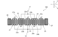
- FIG. 1 is a schematic equivalent circuit diagram of the acoustic wave filter device according to the first embodiment.
- FIG. 2 is a schematic equivalent circuit diagram of an acoustic wave filter device according to a comparative example.
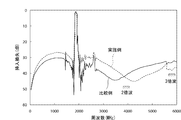
- FIG. 3 is a graph showing the insertion loss of the elastic wave filter device according to the example and the insertion loss of the elastic wave filter device according to the comparative example.
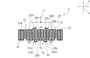
- FIG. 4 is a schematic equivalent circuit diagram of the acoustic wave filter device according to the second embodiment.
- FIG. 5 is a schematic equivalent circuit diagram of the acoustic wave filter device according to the third embodiment.
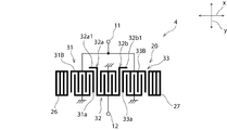
- FIG. 6 is a schematic equivalent circuit diagram of the acoustic wave filter device according to the fourth embodiment.
- FIG. 1 is a schematic equivalent circuit diagram of the acoustic wave filter device according to the first embodiment.
- FIG. 2 is a schematic equivalent circuit diagram of an acoustic wave filter device according to a comparative example.
- FIG. 3 is a graph showing the insertion loss
- FIG. 7 is a schematic equivalent circuit diagram of an acoustic wave filter device according to a fifth embodiment.
- FIG. 8 is a schematic equivalent circuit diagram of the acoustic wave filter device according to the sixth embodiment.
- FIG. 9 is a schematic equivalent circuit diagram of an acoustic wave filter device according to a seventh embodiment.
- FIG. 10 is a schematic equivalent circuit diagram of the acoustic wave filter device according to the eighth embodiment.
- FIG. 1 is a schematic equivalent circuit diagram of an acoustic wave filter device according to this embodiment.
- the acoustic wave filter device 1 includes a first signal terminal 11 and a second signal terminal 12.
- a longitudinally coupled resonator type acoustic wave filter unit 20 is connected between the first signal terminal 11 and the second signal terminal 12.
- the longitudinally coupled resonator type elastic wave filter unit 20 may be constituted by a longitudinally coupled resonator type surface acoustic wave filter unit that uses surface acoustic waves, or a longitudinally coupled resonator type elastic material that uses boundary acoustic waves. You may be comprised by the boundary wave filter part.
- the longitudinally coupled resonator type acoustic wave filter unit 20 is formed on a piezoelectric substrate such as a LiNbO 3 substrate, a LiTaO 3 substrate, or a quartz substrate, and has a plurality of IDT electrodes adjacent to each other in the acoustic wave propagation direction x. .
- the longitudinally coupled resonator-type elastic wave filter unit 20 includes first to fifth IDT electrodes 21 to 25 arranged along the elastic wave propagation direction x.
- the first to fifth IDT electrodes 21 to 25 are arranged in this order along the elastic wave propagation direction x.
- Reflectors 26 and 27 are disposed on both sides of the elastic wave propagation direction x in the region where the first to fifth IDT electrodes 21 to 25 are provided.
- Each of the first to fifth IDT electrodes 21 to 25 is composed of a pair of comb-like electrodes that are interleaved with each other. Each of the pair of comb-like electrodes has a plurality of electrode fingers and a bus bar connecting one end of the plurality of electrode fingers.
- one comb-like electrode of each of the second and fourth IDT electrodes 22 and 24 is connected to the first signal terminal 11, and the other comb
- the tooth electrode is connected to the ground potential.
- One of the first, third and fifth IDT electrodes 21, 23, 25 is connected to the ground potential, and the other comb electrode is connected to the second signal terminal 12. Has been.
- the electrode finger 22 a located closest to the first IDT electrode 21 side of the second IDT electrode 22 is connected to the first signal terminal 11.
- the electrode finger 22 b located closest to the third IDT electrode 23 side of the second IDT electrode 22 is connected to the first signal terminal 11. That is, each of the electrode fingers 22 a and 22 b located on the outermost side of the second IDT electrode 22 is connected to the first signal terminal 11.
- the electrode finger 24 a located closest to the third IDT electrode 23 side of the fourth IDT electrode 24 is connected to the first signal terminal 11.
- the electrode finger 24 b located closest to the fifth IDT electrode 25 side of the fourth IDT electrode 24 is connected to the first signal terminal 11. That is, each of the electrode fingers 24 a and 24 b located on the outermost side of the fourth IDT electrode 24 is connected to the first signal terminal 11.
- the electrode finger 21 a located closest to the second IDT electrode 22 of the first IDT electrode 21 is connected to the second signal terminal 12.
- the electrode finger 25 a located closest to the fourth IDT electrode 24 side of the fifth IDT electrode 25 is connected to the second signal terminal 12.
- the electrode finger 23 a located closest to the second IDT electrode 22 side of the third IDT electrode 23 is connected to the second signal terminal 12.
- the electrode finger 23 b located closest to the fourth IDT electrode 24 side of the third IDT electrode 23 is connected to the second signal terminal 12. That is, each of the electrode fingers 23 a and 23 b located on the outermost side of the third IDT electrode 23 is connected to the second signal terminal 12.
- the electrode finger connected to the signal terminal may be referred to as a hot side electrode finger, and the electrode finger connected to the ground potential may be referred to as a ground side electrode finger.
- each of the electrode fingers 22a, 22b, 24a, and 24b that are hot-side electrode fingers connected to the first signal terminal 11 is in the intersecting width direction y perpendicular to the elastic wave propagation direction x.
- Opposing portions 22a1, 22b1, 24a1, and 24b1 that face adjacent IDT electrodes 21, 23, and 25 are provided.
- the opposing portions 22a1, 22b1, 24a1, 24b1 are arranged in the cross width direction y with the bus bars 21B, 23B, 25B of one comb-like electrode of the IDT electrodes 21, 23, 25 adjacent to the opposing portions 22a1, 22b1, 24a1, 24b1.
- Including facing parts for this reason, at least a part of the facing portions 22a1, 22b1, 24a1, and 24b1 extends along the elastic wave propagation direction x.
- the electrode fingers 21a, 23a, 23b, 25a which are hot-side electrode fingers connected to the second signal terminal 12, are opposed portions 21a1, 23a1 facing the adjacent IDT electrodes 22, 24 in the cross width direction y. , 23b1 and 25a1.
- the facing portions 21a1, 23a1, 23b1, and 25a1 are opposed to the bus bars 22B and 24B of one comb-like electrode of the adjacent IDT electrodes 22 and 24 in the intersecting width direction y, with the facing portions 21a1, 23a1, 23b1, and 25a1. Including parts. For this reason, at least a part of the facing portions 21a1, 23a1, 23b1, and 25a1 extends along the elastic wave propagation direction x.
- the magnitude of the bridging capacitance formed between the electrode fingers 22a, 22b, 24a, 24b, 21a, 23a, 23b, and 25a, which are hot side electrode fingers, and the adjacent IDT electrodes. Can be increased. Thereby, the frequency of the attenuation pole can be shifted to the high frequency side to match the harmonic frequency. Further, it is not always necessary to change the crossing width of the first to fifth IDT electrodes, the pitch of the electrode fingers, or the like, and it is not always necessary to add another element.
- the acoustic wave filter device The filter characteristics in one pass band are not substantially changed. Accordingly, it is possible to increase the attenuation of harmonics such as second harmonic and third harmonic while suppressing increase in insertion loss of the passband of the elastic wave filter device 1.
- the electrode fingers 22a, 22b, 24a, 24b, 21a, 23a, 23b, and 25a are adjacent to the hot electrode fingers of the IDT electrode or the hot bus bar (the first or second signal terminal 11, 12 is opposed to the bus bar of the comb-shaped electrode connected to the terminal 12.
- the length of the portion of the electrode fingers 22a, 22b, 24a, 24b, 21a, 23a, 23b, and 25a facing the adjacent IDT electrodes depends on the frequency of the attenuation pole to be matched with the harmonic frequency. Can be set as appropriate.
- the length of the portion of the electrode fingers 22a, 22b, 24a, 24b, 21a, 23a, 23b, 25a facing the adjacent IDT electrodes is 1.2 to 3.0 times the crossing width of the IDT electrodes 21-25.
- the range is preferably within the range of 1.5 times, and more preferably within the range of 1.5 to 2.0 times.
- the frequency cannot be shifted to the harmonic frequency.
- the electrode fingers 22a, 22b, 24a, 24b, 21a, 23a, 23b, and 25a are provided with facing portions 22a1, 22b1, 24a1, 24b1, 21a1, 23a1, 23b1, and 25a1, so the electrodes
- the lengths of the portions of the fingers 22a, 22b, 24a, 24b, 21a, 23a, 23b, and 25a facing the adjacent IDT electrodes can be made sufficiently larger than the intersection width of the IDT electrodes 21 to 25.
- the length of the portion of the electrode fingers 22a, 22b, 24a, 24b, 21a, 23a, 23b, 25a facing the adjacent IDT electrodes is too large with respect to the crossing width of the IDT electrodes 21 to 25, impedance matching May be difficult. Accordingly, the length of the portion of the electrode fingers 22a, 22b, 24a, 24b, 21a, 23a, 23b, and 25a facing the adjacent IDT electrodes is 3.0 times or less the intersection width of the IDT electrodes 21 to 25. Preferably there is.
- an elastic wave filter device substantially similar to the elastic wave filter device 1 of the first embodiment is manufactured, a signal is input from the first signal terminal 11, and a signal is input from the second signal terminal 12.
- the insertion loss of the acoustic wave filter device 1 was measured. The results are shown in FIG. In FIG. 3, the broken line indicates the insertion loss of this embodiment.
- the length of the portion of the electrode fingers 22a, 22b, 24a, 24b, 21a, 23a, 23b, 25a facing the adjacent IDT electrodes is 1 of the intersection width of the IDT electrodes 21-25. .5 times.
- FIG. 2 As a comparative example, as shown in FIG. 2, it is substantially the same as the elastic wave filter device 1 of the first embodiment except that the facing portions 22a1, 22b1, 24a1, 24b1, 21a1, 23a1, 23b1, and 25a1 are not provided.
- the insertion loss of the acoustic wave filter device 1 when the signal is input from the first signal terminal 11 and the signal is output from the second signal terminal 12 is manufactured. It was measured. The results are shown in FIG. In FIG. 3, the solid line shows the insertion loss of the comparative example.
- FIG. 4 is a schematic equivalent circuit diagram of the acoustic wave filter device according to the second embodiment.
- the elastic wave filter device 1 of the first embodiment has a so-called 5IDT type longitudinally coupled resonator type elastic wave filter unit 20 in which five IDT electrodes 21 to 25 are arranged along the elastic wave propagation direction x. ing.
- An elastic wave filter device according to the present invention includes, for example, a 3IDT electrode type longitudinally coupled resonator type elastic wave filter section in which the number of IDT electrodes arranged along the elastic wave propagation direction is three. Also good.
- the elastic wave filter device according to the present invention has, for example, a 7IDT electrode type longitudinally coupled resonator type elastic wave filter section in which the number of IDT electrodes arranged along the elastic wave propagation direction is seven. Also good.
- the longitudinally coupled resonator type elastic wave filter unit 20 includes three IDT electrodes 31 to 31 arranged in this order along the elastic wave propagation direction x. 33.
- One comb-like electrode of each of the first and third IDT electrodes 31 and 33 located on both sides of the elastic wave propagation direction x is connected to the first signal terminal 11 and the other comb-teeth shape is used.
- the electrode is connected to ground potential.
- One comb-like electrode of the second IDT electrode 32 located in the center of the elastic wave propagation direction x is connected to the ground potential, and the other comb-like electrode is connected to the second signal terminal 12. ing.
- the electrode fingers 31 a and 33 a positioned closest to the IDT electrode 32 of the IDT electrodes 31 and 33 are hot-side electrode fingers connected to the first signal terminal 11.
- the electrode fingers 32 a and 32 b located closest to the IDT electrodes 31 and 33 of the IDT electrode 32 are hot-side electrode fingers connected to the second signal terminal 12.
- Each of the electrode fingers 31a and 33a which are hot-side electrode fingers, has opposing portions 31a1 and 33a1 that face the IDT electrode 32 in the cross width direction y.
- Each of the electrode fingers 32a and 32b, which are hot-side electrode fingers has opposing portions 32a1 and 32b1 that face the IDT electrode 31 or the IDT electrode 33 in the intersecting width direction y.
- each of the facing portions 31a1, 33a1, 32a1, and 32b1 constituting a part of the hot side electrode finger faces the hot side electrode finger and the bus bar connected to the hot side electrode finger. . For this reason, the attenuation amount of harmonics is further increased.
- the opposing portions 31a1 and 33a1 are connected to the bus bar 32B of the comb-like electrode connected to the second signal terminal 12 among the pair of comb-like electrodes constituting the IDT electrode 32. Including facing parts.
- the facing portions 32a1 and 32b1 face the bus bars 31B and 33B of the comb-shaped electrodes connected to the first signal terminal 11 among the pair of comb-shaped electrodes constituting the IDT electrodes 31 and 33. Including parts. For this reason, opposing part 31a1, 33a1, 32a1, 32b1 contains the part extended along the elastic wave propagation
- FIG. 5 is a schematic equivalent circuit diagram of the acoustic wave filter device according to the third embodiment.
- FIG. 6 is a schematic equivalent circuit diagram of the acoustic wave filter device according to the fourth embodiment.
- the outermost electrode fingers of two adjacent IDT electrodes are hot-side electrode fingers and face the adjacent IDT electrodes in the cross width direction.
- the present invention is not limited to this configuration.
- the electrode finger on the other IDT electrode side is a hot-side electrode finger, and only the electrode finger has a facing portion. Good.
- the electrode fingers 21a, 22b, 24a, and 25a have opposing portions 21a1, 22b1, 24a1, and 25a1.
- the electrode fingers 22a, 23a, 23b, and 24b do not have a facing portion.
- the electrode fingers 32a and 32b have the facing portions 32a1 and 32b1, and the electrode fingers 31a and 33a. Does not have a facing part.
- the attenuation of harmonics can be increased while suppressing an increase in insertion loss in the passband.
- FIG. 7 is a schematic equivalent circuit diagram of an acoustic wave filter device according to a fifth embodiment.
- both electrode fingers of IDT electrodes adjacent in the elastic wave propagation direction x are hot-side electrode fingers.
- the present invention is not limited to this configuration.
- the electrode finger on the other IDT electrode side of one IDT electrode of two IDT electrodes adjacent to each other in the elastic wave propagation direction x is a hot side electrode finger
- the most IDT electrode side of the other IDT electrode may be a ground-side electrode finger.
- the electrode fingers 32 a and 32 b on the most IDT electrodes 31 and 33 side of the IDT electrode 32 are hot side electrode fingers.
- the electrode fingers 31a and 33a closest to the IDT electrode 32 of 33 are not hot-side electrode fingers but ground-side electrode fingers.
- Each of the tip portions of the electrode fingers 32a and 32b that are hot-side electrode fingers and the tip portions of the electrode fingers 31a and 33a that are ground-side electrode fingers extend along the elastic wave propagation direction x.
- the tip portions of the electrode fingers 32a and 32b that are hot-side electrode fingers are opposed to the tip portions of the electrode fingers 31a and 33a that are ground-side electrode fingers in the cross width direction y.
- Opposing portions 32a1 and 32b1 are constituted by the tip portions of the electrode fingers 32a and 32b which are the hot side electrode fingers.
- the opposing portions 31a1 and 33a1 are constituted by the tip portions of the electrode fingers 31a and 33a which are ground side electrode fingers.
- the facing portions 32a1 and 32b1 and the facing portions 31a1 and 33a1 face each other in the cross width direction y.
- FIG. 8 is a schematic equivalent circuit diagram of the acoustic wave filter device according to the sixth embodiment.
- FIG. 9 is a schematic equivalent circuit diagram of an acoustic wave filter device according to a seventh embodiment.
- FIG. 10 is a schematic equivalent circuit diagram of the acoustic wave filter device according to the eighth embodiment.
- the acoustic wave filter device according to the present invention may have, for example, one first signal terminal and two second signal terminals. In that case, it is preferable that an input terminal is configured by the first signal terminal, and a balanced output terminal that outputs a balanced signal is configured by the two second signal terminals. That is, the elastic wave filter device according to the present invention may be a balanced elastic wave filter device having a balance-unbalance conversion function.
- the longitudinally coupled resonator type acoustic wave filter unit 20 is configured as an input terminal. 1 signal terminal 11 and two second signal terminals 12a and 12b constituting a balanced output terminal.
- the elastic wave filter devices 6 to 8 having such a configuration, it is possible to increase the attenuation of harmonics while suppressing an increase in insertion loss in the passband.
- the acoustic wave filter device having only one filter unit has been described.
- the elastic wave filter device according to the present invention includes, for example, an elastic wave duplexer having a plurality of filter units, and at least one of the plurality of filter units is configured by a longitudinally coupled resonator type elastic wave filter unit. It may be.
Landscapes
- Physics & Mathematics (AREA)
- Acoustics & Sound (AREA)
- Surface Acoustic Wave Elements And Circuit Networks Thereof (AREA)
Abstract
高調波の減衰量が大きい弾性波フィルタ装置を提供する。 弾性波フィルタ装置1は、第1の信号端子11と、第2の信号端子12と、縦結合共振子型弾性波フィルタ部20とを備えている。縦結合共振子型弾性波フィルタ部20は、第1の信号端子11と第2の信号端子12との間に接続されている。縦結合共振子型弾性波フィルタ部20は、弾性波伝搬方向xに隣り合う第1及び第2のIDT電極22,21を有する。第1のIDT電極22の最も第2のIDT電極21側の電極指である第1の電極指22aは、第1または第2の信号端子11,12に接続されている。第1の電極指22aは、第2のIDT電極21と対向している部分を有し、当該部分は、弾性波伝搬方向xに対して垂直な交差幅方向yにおいて第2のIDT電極21と対向している対向部22a1を含む。
Description
本発明は、弾性波フィルタ装置に関する。特に、本発明は、縦結合共振子型弾性波フィルタ部を有する弾性波フィルタ装置に関する。
近年、携帯電話機などの通信機器に、弾性表面波や弾性境界波などの弾性波を利用した弾性波フィルタ装置が広く用いられるようになってきている。例えば特許文献1には、このような弾性波フィルタ装置として、複数のIDT電極が弾性波伝搬方向に沿って配された縦結合共振子型弾性表面波フィルタ部を有する弾性波フィルタ装置が開示されている。
近年、通信機器のマルチバンド化が急速に進んできている。これに伴い、通信機器に用いられる弾性波フィルタ装置には、通過帯域における挿入損失が小さいのは勿論のこと、通過帯域以外の周波数帯における減衰量が大きいことも強く求められるようになってきている。とりわけ、弾性波フィルタ装置には、2倍波や3倍波などの高調波の減衰量が大きいことが強く求められるようになってきている。
本発明は、斯かる点に鑑みて成されたものであり、その目的は、高調波の減衰量が大きい弾性波フィルタ装置を提供することにある。
本発明に係る弾性波フィルタ装置は、第1の信号端子と、第2の信号端子と、縦結合共振子型弾性波フィルタ部とを備えている。縦結合共振子型弾性波フィルタ部は、第1の信号端子と第2の信号端子との間に接続されている。縦結合共振子型弾性波フィルタ部は、弾性波伝搬方向に隣り合う第1及び第2のIDT電極を有する。第1のIDT電極の最も第2のIDT電極側の電極指である第1の電極指は、第1または第2の信号端子に接続されている。第1の電極指は、第2のIDT電極と対向している部分を有する。第1の電極指の第2のIDT電極と対向している部分は、弾性波伝搬方向に対して垂直な交差幅方向において第2のIDT電極と対向している対向部を含む。
本発明に係る弾性波フィルタ装置のある特定の局面では、第1の電極指の対向部は、第2のIDT電極のバスバーと交差幅方向において対向している部分を含む。
本発明に係る弾性波フィルタ装置の別の特定の局面では、第1の電極指の第2のIDT電極と対向している部分の長さは、第1のIDT電極の交差幅の1.2倍~3.0倍の範囲内である。
本発明に係る弾性波フィルタ装置の他の特定の局面では、第2のIDT電極の最も第1のIDT電極側の電極指である第2の電極指は、第1のIDT電極と対向している部分を有する。第2の電極指の第1のIDT電極と対向している部分は、交差幅方向において第1のIDT電極と対向している対向部を含む。
本発明に係る弾性波フィルタ装置のさらに他の特定の局面では、第2の電極指の対向部は、第1のIDT電極のバスバーと交差幅方向において対向している部分を含む。
本発明に係る弾性波フィルタ装置のさらに別の特定の局面では、第1の電極指の第2のIDT電極と対向している部分と、第2の電極指の第1のIDT電極と対向している部分とは、交差幅方向において互いに対向している部分を含む。
本発明に係る弾性波フィルタ装置のまたさらに他の特定の局面では、第2の電極指は、第1または第2の信号端子に接続されている。
本発明によれば、高調波の減衰量が大きい弾性波フィルタ装置を提供することができる。
以下、本発明を実施した好ましい形態の一例について説明する。但し、下記の実施形態は、単なる例示である。本発明は、下記の実施形態に何ら限定されない。
また、実施形態等において参照する各図面において、実質的に同一の機能を有する部材は同一の符号で参照することとする。また、実施形態等において参照する図面は、模式的に記載されたものであり、図面に描画された物体の寸法の比率などは、現実の物体の寸法の比率などとは異なる場合がある。図面相互間においても、物体の寸法比率等が異なる場合がある。具体的な物体の寸法比率等は、以下の説明を参酌して判断されるべきである。
(第1の実施形態)
図1は、本実施形態に係る弾性波フィルタ装置の略図的等価回路図である。
図1は、本実施形態に係る弾性波フィルタ装置の略図的等価回路図である。
図1に示すように、弾性波フィルタ装置1は、第1の信号端子11と第2の信号端子12とを有する。第1の信号端子11と第2の信号端子12との間には、縦結合共振子型弾性波フィルタ部20が接続されている。この縦結合共振子型弾性波フィルタ部20は、弾性表面波を利用した縦結合共振子型弾性表面波フィルタ部により構成されていてもよいし、弾性境界波を利用した縦結合共振子型弾性境界波フィルタ部により構成されていてもよい。
縦結合共振子型弾性波フィルタ部20は、例えば、LiNbO3基板、LiTaO3基板、水晶基板等の圧電基板の上に形成されており、弾性波伝搬方向xに隣り合う複数のIDT電極を有する。具体的には、縦結合共振子型弾性波フィルタ部20は、弾性波伝搬方向xに沿って配列されている第1~第5のIDT電極21~25を有する。第1~第5のIDT電極21~25は、弾性波伝搬方向xに沿ってこの順番で配列されている。第1~第5のIDT電極21~25が設けられている領域の弾性波伝搬方向xの両側には、反射器26,27が配されている。
第1~第5のIDT電極21~25のそれぞれは、互いに間挿し合っている一対のくし歯状電極により構成されている。一対のくし歯状電極のそれぞれは、複数の電極指と、複数の電極指の一方の端部を接続するバスバーとを有する。第1~第5のIDT電極21~25のうち、第2及び第4のIDT電極22,24のそれぞれの一方のくし歯状電極が第1の信号端子11に接続されており、他方のくし歯状電極がグラウンド電位に接続されている。第1,第3及び第5のIDT電極21,23,25のそれぞれの一方のくし歯状電極はグラウンド電位に接続されており、他方のくし歯状電極は、第2の信号端子12に接続されている。
第2のIDT電極22の最も第1のIDT電極21側に位置している電極指22aは、第1の信号端子11に接続されている。第2のIDT電極22の最も第3のIDT電極23側に位置している電極指22bは、第1の信号端子11に接続されている。すなわち、第2のIDT電極22の最も外側に位置している電極指22a、22bのそれぞれは、第1の信号端子11に接続されている。
第4のIDT電極24の最も第3のIDT電極23側に位置している電極指24aは、第1の信号端子11に接続されている。第4のIDT電極24の最も第5のIDT電極25側に位置している電極指24bは、第1の信号端子11に接続されている。すなわち、第4のIDT電極24の最も外側に位置している電極指24a、24bのそれぞれは、第1の信号端子11に接続されている。
第1のIDT電極21の最も第2のIDT電極22側に位置している電極指21aは、第2の信号端子12に接続されている。第5のIDT電極25の最も第4のIDT電極24側に位置している電極指25aは、第2の信号端子12に接続されている。
第3のIDT電極23の最も第2のIDT電極22側に位置している電極指23aは、第2の信号端子12に接続されている。第3のIDT電極23の最も第4のIDT電極24側に位置している電極指23bは、第2の信号端子12に接続されている。すなわち、第3のIDT電極23の最も外側に位置している電極指23a、23bのそれぞれは、第2の信号端子12に接続されている。
なお、以下の説明において、信号端子に接続されている電極指をホット側電極指とし、グラウンド電位に接続されている電極指をアース側電極指とすることがある。
本実施形態では、第1の信号端子11に接続されたホット側電極指である電極指22a、22b、24a、24bのそれぞれは、弾性波伝搬方向xに対して垂直な交差幅方向yにおいて、隣り合うIDT電極21,23,25と対向している対向部22a1,22b1,24a1,24b1を有する。対向部22a1,22b1,24a1,24b1は、対向部22a1,22b1,24a1,24b1が隣り合うIDT電極21,23,25の一方のくし歯状電極のバスバー21B,23B,25Bと交差幅方向yにおいて対向している部分を含む。このため、対向部22a1,22b1,24a1,24b1の少なくとも一部は、弾性波伝搬方向xに沿って延びている。
第2の信号端子12に接続されたホット側電極指である電極指21a、23a、23b、25aは、交差幅方向yにおいて、隣り合うIDT電極22,24と対向している対向部21a1,23a1,23b1,25a1を有する。対向部21a1,23a1,23b1,25a1は、対向部21a1,23a1,23b1,25a1が隣り合うIDT電極22,24の一方のくし歯状電極のバスバー22B,24Bと交差幅方向yにおいて対向している部分を含む。このため、対向部21a1,23a1,23b1,25a1の少なくとも一部は、弾性波伝搬方向xに沿って延びている。
このように、本実施形態では、ホット側電極指である電極指22a、22b、24a、24b、21a、23a、23b、25aと隣り合うIDT電極との間に形成される橋絡容量の大きさを大きくすることができる。これにより、減衰極の周波数を高域側にシフトさせ、高調波の周波数に合致させることができる。また、第1~第5のIDT電極の交差幅や、電極指のピッチ等を変化させる必要は必ずしもなく、他の素子をさらに追加する必要も必ずしもない。よって、電極指22a、22b、24a、24b、21a、23a、23b、25aに対向部22a1,22b1,24a1,24b1,21a1,23a1,23b1,25a1を設けた場合であっても、弾性波フィルタ装置1の通過帯域におけるフィルタ特性は実質的に変化しない。従って、弾性波フィルタ装置1の通過帯域の挿入損失の増大を抑制しつつ、2倍波や3倍波などの高調波の減衰量を大きくすることができる。
また、高調波の減衰量を大きくするために他の素子を追加する必要が必ずしもない。このため、弾性波フィルタ装置1が大型化することを抑制することができる。
また、本実施形態では、電極指22a、22b、24a、24b、21a、23a、23b、25aが隣り合うIDT電極のホット側電極指またはホット側のバスバー(第1または第2の信号端子11,12に接続されているくし歯状電極のバスバー)と対向している。
電極指22a、22b、24a、24b、21a、23a、23b、25aの隣り合うIDT電極と対向している部分の長さは、高調波の周波数に合致させようとする減衰極の周波数等に応じて適宜設定することができる。電極指22a、22b、24a、24b、21a、23a、23b、25aの隣り合うIDT電極と対向している部分の長さは、IDT電極21~25の交差幅の1.2倍~3.0倍の範囲内であることが好ましく、1.5倍~2.0倍の範囲内であることがより好ましい。電極指22a、22b、24a、24b、21a、23a、23b、25aの隣り合うIDT電極と対向している部分の長さはIDT電極21~25の交差幅より十分に大きくないと、減衰極の周波数を高調波の周波数までシフトすることができない場合がある。しかし、本実施形態では、電極指22a、22b、24a、24b、21a、23a、23b、25aに対向部22a1,22b1,24a1,24b1,21a1,23a1,23b1,25a1が設けられているので、電極指22a、22b、24a、24b、21a、23a、23b、25aの隣り合うIDT電極と対向している部分の長さをIDT電極21~25の交差幅より十分に大きくすることができる。
電極指22a、22b、24a、24b、21a、23a、23b、25aの隣り合うIDT電極と対向している部分の長さがIDT電極21~25の交差幅に対して大きすぎると、インピーダンスの整合が困難になる場合がある。従って、電極指22a、22b、24a、24b、21a、23a、23b、25aの隣り合うIDT電極と対向している部分の長さは、IDT電極21~25の交差幅の3.0倍以下であることが好ましい。
以下、この効果について具体的な例に基づいてさらに詳細に説明する。
実施例として、上記第1の実施形態の弾性波フィルタ装置1と実質的に同様の弾性波フィルタ装置を作製し、第1の信号端子11から信号を入力し、第2の信号端子12から信号を出力させたときの弾性波フィルタ装置1の挿入損失を測定した。結果を図3に示す。図3において、破線が本実施例の挿入損失を示している。
なお、実施例においては、電極指22a、22b、24a、24b、21a、23a、23b、25aの隣り合うIDT電極と対向している部分の長さは、IDT電極21~25の交差幅の1.5倍とした。
比較例として、図2に示すように、対向部22a1,22b1,24a1,24b1,21a1,23a1,23b1,25a1を設けなかったこと以外は、第1の実施形態の弾性波フィルタ装置1と実質的に同様の構成を有する弾性波フィルタ装置100を作製し、第1の信号端子11から信号を入力し、第2の信号端子12から信号を出力させたときの弾性波フィルタ装置1の挿入損失を測定した。結果を図3に示す。図3において、実線が比較例の挿入損失を示している。
なお、実施例及び比較例の説明において、第1の実施形態と実質的に同様の機能を有する部材を同様の符号で参照することとする。
図3に示す結果から、対向部22a1,22b1,24a1,24b1,21a1,23a1,23b1,25a1を設けることにより、2倍波及び3倍波の減衰量を大きくできることが分かる。
以下、本発明の好ましい実施形態の他の例について説明する。以下の説明において、上記第1の実施形態と実質的に共通の機能を有する部材を共通の符号で参照し、説明を省略する。
(第2の実施形態)
図4は、第2の実施形態に係る弾性波フィルタ装置の略図的等価回路図である。
図4は、第2の実施形態に係る弾性波フィルタ装置の略図的等価回路図である。
第1の実施形態の弾性波フィルタ装置1は、弾性波伝搬方向xに沿って5つのIDT電極21~25が配列されている所謂5IDT型の縦結合共振子型弾性波フィルタ部20を有している。但し、本発明は、これに限定されない。本発明に係る弾性波フィルタ装置は、例えば弾性波伝搬方向に沿って配列されているIDT電極の数量が3つである3IDT電極型の縦結合共振子型弾性波フィルタ部を有するものであってもよい。本発明に係る弾性波フィルタ装置は、例えば弾性波伝搬方向に沿って配列されているIDT電極の数量が7つである7IDT電極型の縦結合共振子型弾性波フィルタ部を有するものであってもよい。
図4に示すように、本実施形態の弾性波フィルタ装置2では、縦結合共振子型弾性波フィルタ部20は、弾性波伝搬方向xに沿ってこの順番で配列された3つのIDT電極31~33を有する。弾性波伝搬方向xの両側に位置している第1及び第3のIDT電極31,33のそれぞれの一方のくし歯状電極が第1の信号端子11に接続されており、他方のくし歯状電極がグラウンド電位に接続されている。弾性波伝搬方向xの中央に位置している第2のIDT電極32の一方のくし歯状電極がグラウンド電位に接続されており、他方のくし歯状電極が第2の信号端子12に接続されている。
IDT電極31,33の最もIDT電極32側に位置している電極指31a、33aは、第1の信号端子11に接続されているホット側電極指である。IDT電極32の最もIDT電極31,33側に位置している電極指32a、32bは、第2の信号端子12に接続されているホット側電極指である。
ホット側電極指である電極指31a、33aのそれぞれは、交差幅方向yにおいてIDT電極32と対向している対向部31a1,33a1を有する。ホット側電極指である電極指32a、32bのそれぞれは、交差幅方向yにおいてIDT電極31またはIDT電極33と対向している対向部32a1,32b1を有する。このため、第1の実施形態の弾性波フィルタ装置1と同様に、本実施形態の弾性波フィルタ装置2においても、通過帯域における挿入損失が小さいと共に、高調波の減衰量が大きい。
本実施形態においても、ホット側電極指の一部を構成している対向部31a1,33a1,32a1,32b1のそれぞれがホット側電極指及びホット側電極指に接続されているバスバーと対向している。このため、高調波の減衰量がさらに大きくなっている。
なお、本実施形態では、対向部31a1,33a1は、IDT電極32を構成している一対のくし歯状電極のうち、第2の信号端子12に接続されているくし歯状電極のバスバー32Bと対向している部分を含む。対向部32a1,32b1は、IDT電極31,33を構成している一対のくし歯状電極のうち、第1の信号端子11に接続されているくし歯状電極のバスバー31B,33Bと対向している部分を含む。このため、対向部31a1,33a1,32a1,32b1は、弾性波伝搬方向xに沿って延びる部分を含む。
(第3及び第4の実施形態)
図5は、第3の実施形態に係る弾性波フィルタ装置の略図的等価回路図である。図6は、第4の実施形態に係る弾性波フィルタ装置の略図的等価回路図である。
図5は、第3の実施形態に係る弾性波フィルタ装置の略図的等価回路図である。図6は、第4の実施形態に係る弾性波フィルタ装置の略図的等価回路図である。
第1及び第2の実施形態では、隣り合う2つのIDT電極の両方の最も外側の電極指がホット側電極指であると共に、隣り合うIDT電極と交差幅方向において対向している例について説明した。但し、本発明は、この構成に限定されない。隣り合う2つのIDT電極の一方のIDT電極の複数の電極指のうちの最も他方のIDT電極側の電極指が、ホット側電極指であり、当該電極指のみが対向部を有していてもよい。
図5に示す第3の実施形態に係る弾性波フィルタ装置3では、第1の実施形態とは異なり、電極指21a、22b、24a、25aのみが対向部21a1,22b1,24a1,25a1を有しており、電極指22a、23a、23b、24bは対向部を有していない。
図6に示す第4の実施形態に係る弾性波フィルタ装置4では、第2の実施形態とは異なり、電極指32a、32bのみが対向部32a1,32b1を有しており、電極指31a、33aは対向部を有していない。
これらの場合であっても、通過帯域の挿入損失の増大を抑制しつつ、高調波の減衰を大きくすることができる。
(第5の実施形態)
図7は、第5の実施形態に係る弾性波フィルタ装置の略図的等価回路図である。
図7は、第5の実施形態に係る弾性波フィルタ装置の略図的等価回路図である。
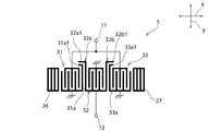
第1~第4の実施形態では、弾性波伝搬方向xにおいて隣り合うIDT電極の電極指の両方がホット側電極指である例について説明した。但し、本発明は、この構成に限定されない。例えば、弾性波伝搬方向xにおいて隣り合う2つのIDT電極の一方のIDT電極の最も他方のIDT電極側の電極指がホット側電極指であれば、他方のIDT電極の最も一方のIDT電極側の電極指はアース側電極指であってもよい。
例えば図7に示す第5の実施形態に係る弾性波フィルタ装置5では、IDT電極32の最もIDT電極31,33側の電極指32a、32bは、ホット側電極指であるが、IDT電極31,33の最もIDT電極32側の電極指31a、33aは、ホット側電極指ではなく、アース側電極指である。ホット側電極指である電極指32a、32bの先端部と、アース側電極指である電極指31a、33aの先端部とのそれぞれは、弾性波伝搬方向xに沿って延びている。ホット側電極指である電極指32a、32bの先端部は、アース側電極指である電極指31a、33aの先端部と交差幅方向yにおいて対向している。このホット側電極指である電極指32a、32bの先端部により対向部32a1,32b1が構成されている。同時に、アース側電極指である電極指31a、33aの先端部により対向部31a1,33a1が構成されている。対向部32a1,32b1と対向部31a1,33a1とは、交差幅方向yにおいて互いに対向している。
このような構成を有する弾性波フィルタ装置5においても、通過帯域の挿入損失の増大を抑制しつつ、高調波の減衰を大きくすることができる。
(第6~第8の実施形態)
図8は、第6の実施形態に係る弾性波フィルタ装置の略図的等価回路図である。図9は、第7の実施形態に係る弾性波フィルタ装置の略図的等価回路図である。図10は、第8の実施形態に係る弾性波フィルタ装置の略図的等価回路図である。
図8は、第6の実施形態に係る弾性波フィルタ装置の略図的等価回路図である。図9は、第7の実施形態に係る弾性波フィルタ装置の略図的等価回路図である。図10は、第8の実施形態に係る弾性波フィルタ装置の略図的等価回路図である。
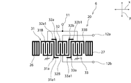
第1~第5の実施形態では、第1の信号端子11と第2の信号端子12とが一つずつ設けられている例について説明した。但し、本発明は、これに限定されない。本発明に係る弾性波フィルタ装置は、例えば、一つの第1の信号端子と、二つの第2の信号端子とを有するものであってもよい。その場合、第1の信号端子により入力端子が構成されており、二つの第2の信号端子により平衡信号を出力する平衡出力端子が構成されていることが好ましい。すなわち、本発明に係る弾性波フィルタ装置は、平衡-不平衡変換機能を有するバランス型の弾性波フィルタ装置であってもよい。
具体的には、図8~10に示す第6~第8の実施形態に係る弾性波フィルタ装置6~8では、縦結合共振子型弾性波フィルタ部20は、入力端子を構成している第1の信号端子11と、平衡出力端子を構成している二つの第2の信号端子12a、12bとの間に接続されている。
このような構成を有する弾性波フィルタ装置6~8においても、通過帯域の挿入損失の増大を抑制しつつ、高調波の減衰を大きくすることができる。
なお、第1~第8の実施形態では、一つのフィルタ部のみを有する弾性波フィルタ装置について説明した。但し、本発明は、これに限定されない。本発明に係る弾性波フィルタ装置は、例えば、複数のフィルタ部を有し、それら複数のフィルタ部の内の少なくとも一つが縦結合共振子型弾性波フィルタ部により構成されている弾性波分波器であってもよい。
1~8…弾性波フィルタ装置
11…第1の信号端子
12、12a、12b…第2の信号端子
20…縦結合共振子型弾性波フィルタ部
21~25,31~33…IDT電極
21B,22B,23B,24B,25B,31B,32B,33B…バスバー
21a、22a、22b、23a、23b、24a、24b、25a、31a、32a、32b、33a…電極指
21a1、22a1、22b1、23a1、23b1、24a1、24b1、25a1、31a1、32a1、32b1、33a1…対向部
26,27…反射器
11…第1の信号端子
12、12a、12b…第2の信号端子
20…縦結合共振子型弾性波フィルタ部
21~25,31~33…IDT電極
21B,22B,23B,24B,25B,31B,32B,33B…バスバー
21a、22a、22b、23a、23b、24a、24b、25a、31a、32a、32b、33a…電極指
21a1、22a1、22b1、23a1、23b1、24a1、24b1、25a1、31a1、32a1、32b1、33a1…対向部
26,27…反射器
Claims (7)
- 第1の信号端子と、
第2の信号端子と、
前記第1の信号端子と前記第2の信号端子との間に接続されており、弾性波伝搬方向に隣り合う第1及び第2のIDT電極を有する縦結合共振子型弾性波フィルタ部と、
を備え、
前記第1のIDT電極の最も前記第2のIDT電極側の電極指である第1の電極指は、前記第1または第2の信号端子に接続されており、
前記第1の電極指は、前記第2のIDT電極と対向している部分を有し、前記第1の電極指の前記第2のIDT電極と対向している部分は弾性波伝搬方向に対して垂直な交差幅方向において前記第2のIDT電極と対向している対向部を含む、弾性波フィルタ装置。 - 前記第1の電極指の対向部は、前記第2のIDT電極のバスバーと交差幅方向において対向している部分を含む、請求項1に記載の弾性波フィルタ装置。
- 前記第1の電極指の前記第2のIDT電極と対向している部分の長さは、前記第1のIDT電極の交差幅の1.2倍~3.0倍の範囲内である、請求項1または2に記載の弾性波フィルタ装置。
- 前記第2のIDT電極の最も前記第1のIDT電極側の電極指である第2の電極指は前記第1のIDT電極と対向している部分を有し、前記第2の電極指の前記第1のIDT電極と対向している部分は交差幅方向において前記第1のIDT電極と対向している対向部を含む、請求項1に記載の弾性波フィルタ装置。
- 前記第2の電極指の対向部は、前記第1のIDT電極のバスバーと交差幅方向において対向している部分を含む、請求項4に記載の弾性波フィルタ装置。
- 前記第1の電極指の前記第2のIDT電極と対向している部分と前記第2の電極指の前記第1のIDT電極と対向している部分とは、交差幅方向において互いに対向している部分を含む、請求項4に記載の弾性波フィルタ装置。
- 前記第2の電極指は、前記第1または第2の信号端子に接続されている、請求項4~6のいずれか一項に記載の弾性波フィルタ装置。
Applications Claiming Priority (2)
| Application Number | Priority Date | Filing Date | Title |
|---|---|---|---|
| JP2011115313 | 2011-05-24 | ||
| JP2011-115313 | 2011-05-24 |
Publications (1)
| Publication Number | Publication Date |
|---|---|
| WO2012160730A1 true WO2012160730A1 (ja) | 2012-11-29 |
Family
ID=47216825
Family Applications (1)
| Application Number | Title | Priority Date | Filing Date |
|---|---|---|---|
| PCT/JP2011/079817 Ceased WO2012160730A1 (ja) | 2011-05-24 | 2011-12-22 | 弾性波フィルタ装置 |
Country Status (1)
| Country | Link |
|---|---|
| WO (1) | WO2012160730A1 (ja) |
Cited By (3)
| Publication number | Priority date | Publication date | Assignee | Title |
|---|---|---|---|---|
| KR20170121704A (ko) | 2016-04-25 | 2017-11-02 | 가부시키가이샤 무라타 세이사쿠쇼 | 탄성파 장치 |
| US9970325B2 (en) | 2015-04-30 | 2018-05-15 | General Electric Company | Jacking assembly for rotor |
| US20200021267A1 (en) * | 2018-07-16 | 2020-01-16 | Qorvo Us, Inc. | Interdigital transducer arrangements for surface acoustic wave devices |
Citations (6)
| Publication number | Priority date | Publication date | Assignee | Title |
|---|---|---|---|---|
| JPS55141813A (en) * | 1979-04-24 | 1980-11-06 | Murata Mfg Co Ltd | Surface acoustic wave device |
| JP2002314367A (ja) * | 2001-04-16 | 2002-10-25 | Murata Mfg Co Ltd | 弾性表面波装置、通信装置 |
| JP2002359537A (ja) * | 2001-06-01 | 2002-12-13 | Murata Mfg Co Ltd | 弾性表面波フィルタ、通信装置 |
| JP2003309452A (ja) * | 2000-04-18 | 2003-10-31 | Murata Mfg Co Ltd | 縦結合共振子型弾性表面波フィルタ |
| JP2008067032A (ja) * | 2006-09-07 | 2008-03-21 | Epson Toyocom Corp | 平衡型弾性表面波フィルタ |
| JP2008086051A (ja) * | 2007-12-21 | 2008-04-10 | Seiko Epson Corp | 弾性表面波フィルタおよび弾性表面波共振器 |
-
2011
- 2011-12-22 WO PCT/JP2011/079817 patent/WO2012160730A1/ja not_active Ceased
Patent Citations (6)
| Publication number | Priority date | Publication date | Assignee | Title |
|---|---|---|---|---|
| JPS55141813A (en) * | 1979-04-24 | 1980-11-06 | Murata Mfg Co Ltd | Surface acoustic wave device |
| JP2003309452A (ja) * | 2000-04-18 | 2003-10-31 | Murata Mfg Co Ltd | 縦結合共振子型弾性表面波フィルタ |
| JP2002314367A (ja) * | 2001-04-16 | 2002-10-25 | Murata Mfg Co Ltd | 弾性表面波装置、通信装置 |
| JP2002359537A (ja) * | 2001-06-01 | 2002-12-13 | Murata Mfg Co Ltd | 弾性表面波フィルタ、通信装置 |
| JP2008067032A (ja) * | 2006-09-07 | 2008-03-21 | Epson Toyocom Corp | 平衡型弾性表面波フィルタ |
| JP2008086051A (ja) * | 2007-12-21 | 2008-04-10 | Seiko Epson Corp | 弾性表面波フィルタおよび弾性表面波共振器 |
Cited By (6)
| Publication number | Priority date | Publication date | Assignee | Title |
|---|---|---|---|---|
| US9970325B2 (en) | 2015-04-30 | 2018-05-15 | General Electric Company | Jacking assembly for rotor |
| US10344625B2 (en) | 2015-04-30 | 2019-07-09 | General Electric Company | Jacking assembly for rotor |
| KR20170121704A (ko) | 2016-04-25 | 2017-11-02 | 가부시키가이샤 무라타 세이사쿠쇼 | 탄성파 장치 |
| US10193529B2 (en) | 2016-04-25 | 2019-01-29 | Murata Manufacturing Co., Ltd. | Elastic wave device |
| US20200021267A1 (en) * | 2018-07-16 | 2020-01-16 | Qorvo Us, Inc. | Interdigital transducer arrangements for surface acoustic wave devices |
| US10938373B2 (en) * | 2018-07-16 | 2021-03-02 | Qorvo Us, Inc. | Interdigital transducer arrangements for surface acoustic wave devices |
Similar Documents
| Publication | Publication Date | Title |
|---|---|---|
| JP4631972B2 (ja) | 弾性波フィルタ装置 | |
| JP5333650B2 (ja) | 弾性波装置 | |
| JP5397477B2 (ja) | ラダー型弾性波フィルタ装置及び分波器 | |
| JP4569713B2 (ja) | 弾性波共振器、弾性波フィルタおよびこれを用いたアンテナ共用器 | |
| JPWO2015002047A1 (ja) | 弾性表面波共振器及び弾性表面波フィルタ装置 | |
| JP6465047B2 (ja) | 弾性波共振子、帯域通過型フィルタ及びデュプレクサ | |
| WO2015198709A1 (ja) | ラダー型フィルタ | |
| JP4571200B2 (ja) | 弾性波フィルタ | |
| JP5369197B2 (ja) | 弾性波装置 | |
| JP5045760B2 (ja) | 弾性波フィルタ装置 | |
| KR101974830B1 (ko) | 탄성파 공진자, 탄성파 필터 및 듀플렉서 | |
| WO2006068086A1 (ja) | バランス型sawフィルタ | |
| JPWO2016063718A1 (ja) | 弾性波共振子及びラダー型フィルタ | |
| JP4900420B2 (ja) | 弾性波装置 | |
| WO2012160730A1 (ja) | 弾性波フィルタ装置 | |
| KR101711756B1 (ko) | 탄성파 디바이스, 필터 및 분파기 | |
| WO2013136757A1 (ja) | 弾性波装置 | |
| JP2008035007A (ja) | フィルタ | |
| JP4936102B2 (ja) | 弾性表面波デバイス | |
| CN203406841U (zh) | 用于数字电视的声表面波滤波器 | |
| JP5086140B2 (ja) | 弾性波フィルタ | |
| WO2010140456A1 (ja) | 弾性波共振子、ラダー型フィルタ及びデュプレクサ | |
| JP4995923B2 (ja) | 弾性境界波デバイス、およびそれを用いた通信機 | |
| WO2008053651A1 (en) | Surface acoustic wave filter device and duplexer | |
| JP2013247376A (ja) | 縦結合型弾性表面波フィルタ及び縦続接続型フィルタ |
Legal Events
| Date | Code | Title | Description |
|---|---|---|---|
| 121 | Ep: the epo has been informed by wipo that ep was designated in this application |
Ref document number: 11865967 Country of ref document: EP Kind code of ref document: A1 |
|
| NENP | Non-entry into the national phase |
Ref country code: DE |
|
| 122 | Ep: pct application non-entry in european phase |
Ref document number: 11865967 Country of ref document: EP Kind code of ref document: A1 |
|
| NENP | Non-entry into the national phase |
Ref country code: JP |