WO2012157740A1 - 高誘電性ナノシート積層体及び高誘電体素子とその製造方法 - Google Patents
高誘電性ナノシート積層体及び高誘電体素子とその製造方法 Download PDFInfo
- Publication number
- WO2012157740A1 WO2012157740A1 PCT/JP2012/062765 JP2012062765W WO2012157740A1 WO 2012157740 A1 WO2012157740 A1 WO 2012157740A1 JP 2012062765 W JP2012062765 W JP 2012062765W WO 2012157740 A1 WO2012157740 A1 WO 2012157740A1
- Authority
- WO
- WIPO (PCT)
- Prior art keywords
- high dielectric
- nanosheet
- perovskite
- substrate
- thin film
- Prior art date
- Legal status (The legal status is an assumption and is not a legal conclusion. Google has not performed a legal analysis and makes no representation as to the accuracy of the status listed.)
- Ceased
Links
Images
Classifications
-
- B—PERFORMING OPERATIONS; TRANSPORTING
- B32—LAYERED PRODUCTS
- B32B—LAYERED PRODUCTS, i.e. PRODUCTS BUILT-UP OF STRATA OF FLAT OR NON-FLAT, e.g. CELLULAR OR HONEYCOMB, FORM
- B32B18/00—Layered products essentially comprising ceramics, e.g. refractory products
-
- H—ELECTRICITY
- H01—ELECTRIC ELEMENTS
- H01G—CAPACITORS; CAPACITORS, RECTIFIERS, DETECTORS, SWITCHING DEVICES, LIGHT-SENSITIVE OR TEMPERATURE-SENSITIVE DEVICES OF THE ELECTROLYTIC TYPE
- H01G4/00—Fixed capacitors; Processes of their manufacture
- H01G4/002—Details
- H01G4/018—Dielectrics
- H01G4/06—Solid dielectrics
- H01G4/08—Inorganic dielectrics
- H01G4/10—Metal-oxide dielectrics
-
- B—PERFORMING OPERATIONS; TRANSPORTING
- B82—NANOTECHNOLOGY
- B82Y—SPECIFIC USES OR APPLICATIONS OF NANOSTRUCTURES; MEASUREMENT OR ANALYSIS OF NANOSTRUCTURES; MANUFACTURE OR TREATMENT OF NANOSTRUCTURES
- B82Y30/00—Nanotechnology for materials or surface science, e.g. nanocomposites
-
- C—CHEMISTRY; METALLURGY
- C01—INORGANIC CHEMISTRY
- C01G—COMPOUNDS CONTAINING METALS NOT COVERED BY SUBCLASSES C01D OR C01F
- C01G33/00—Compounds of niobium
- C01G33/006—Compounds containing niobium, with or without oxygen or hydrogen, and containing two or more other elements
-
- C—CHEMISTRY; METALLURGY
- C01—INORGANIC CHEMISTRY
- C01G—COMPOUNDS CONTAINING METALS NOT COVERED BY SUBCLASSES C01D OR C01F
- C01G35/00—Compounds of tantalum
- C01G35/006—Compounds containing tantalum, with or without oxygen or hydrogen, and containing two or more other elements
-
- C—CHEMISTRY; METALLURGY
- C04—CEMENTS; CONCRETE; ARTIFICIAL STONE; CERAMICS; REFRACTORIES
- C04B—LIME, MAGNESIA; SLAG; CEMENTS; COMPOSITIONS THEREOF, e.g. MORTARS, CONCRETE OR LIKE BUILDING MATERIALS; ARTIFICIAL STONE; CERAMICS; REFRACTORIES; TREATMENT OF NATURAL STONE
- C04B35/00—Shaped ceramic products characterised by their composition; Ceramics compositions; Processing powders of inorganic compounds preparatory to the manufacturing of ceramic products
- C04B35/01—Shaped ceramic products characterised by their composition; Ceramics compositions; Processing powders of inorganic compounds preparatory to the manufacturing of ceramic products based on oxide ceramics
- C04B35/495—Shaped ceramic products characterised by their composition; Ceramics compositions; Processing powders of inorganic compounds preparatory to the manufacturing of ceramic products based on oxide ceramics based on vanadium, niobium, tantalum, molybdenum or tungsten oxides or solid solutions thereof with other oxides, e.g. vanadates, niobates, tantalates, molybdates or tungstates
-
- C—CHEMISTRY; METALLURGY
- C04—CEMENTS; CONCRETE; ARTIFICIAL STONE; CERAMICS; REFRACTORIES
- C04B—LIME, MAGNESIA; SLAG; CEMENTS; COMPOSITIONS THEREOF, e.g. MORTARS, CONCRETE OR LIKE BUILDING MATERIALS; ARTIFICIAL STONE; CERAMICS; REFRACTORIES; TREATMENT OF NATURAL STONE
- C04B35/00—Shaped ceramic products characterised by their composition; Ceramics compositions; Processing powders of inorganic compounds preparatory to the manufacturing of ceramic products
- C04B35/622—Forming processes; Processing powders of inorganic compounds preparatory to the manufacturing of ceramic products
- C04B35/626—Preparing or treating the powders individually or as batches ; preparing or treating macroscopic reinforcing agents for ceramic products, e.g. fibres; mechanical aspects section B
- C04B35/62605—Treating the starting powders individually or as mixtures
- C04B35/62685—Treating the starting powders individually or as mixtures characterised by the order of addition of constituents or additives
-
- H—ELECTRICITY
- H10—SEMICONDUCTOR DEVICES; ELECTRIC SOLID-STATE DEVICES NOT OTHERWISE PROVIDED FOR
- H10D—INORGANIC ELECTRIC SEMICONDUCTOR DEVICES
- H10D1/00—Resistors, capacitors or inductors
- H10D1/60—Capacitors
- H10D1/68—Capacitors having no potential barriers
- H10D1/682—Capacitors having no potential barriers having dielectrics comprising perovskite structures
- H10D1/684—Capacitors having no potential barriers having dielectrics comprising perovskite structures the dielectrics comprising multiple layers, e.g. comprising buffer layers, seed layers or gradient layers
-
- H—ELECTRICITY
- H10—SEMICONDUCTOR DEVICES; ELECTRIC SOLID-STATE DEVICES NOT OTHERWISE PROVIDED FOR
- H10D—INORGANIC ELECTRIC SEMICONDUCTOR DEVICES
- H10D84/00—Integrated devices formed in or on semiconductor substrates that comprise only semiconducting layers, e.g. on Si wafers or on GaAs-on-Si wafers
- H10D84/01—Manufacture or treatment
- H10D84/0123—Integrating together multiple components covered by H10D12/00 or H10D30/00, e.g. integrating multiple IGBTs
- H10D84/0126—Integrating together multiple components covered by H10D12/00 or H10D30/00, e.g. integrating multiple IGBTs the components including insulated gates, e.g. IGFETs
- H10D84/0144—Manufacturing their gate insulating layers
-
- H—ELECTRICITY
- H10—SEMICONDUCTOR DEVICES; ELECTRIC SOLID-STATE DEVICES NOT OTHERWISE PROVIDED FOR
- H10D—INORGANIC ELECTRIC SEMICONDUCTOR DEVICES
- H10D84/00—Integrated devices formed in or on semiconductor substrates that comprise only semiconducting layers, e.g. on Si wafers or on GaAs-on-Si wafers
- H10D84/201—Integrated devices formed in or on semiconductor substrates that comprise only semiconducting layers, e.g. on Si wafers or on GaAs-on-Si wafers characterised by the integration of only components covered by H10D1/00 or H10D8/00, e.g. RLC circuits
- H10D84/204—Integrated devices formed in or on semiconductor substrates that comprise only semiconducting layers, e.g. on Si wafers or on GaAs-on-Si wafers characterised by the integration of only components covered by H10D1/00 or H10D8/00, e.g. RLC circuits of combinations of diodes or capacitors or resistors
- H10D84/212—Integrated devices formed in or on semiconductor substrates that comprise only semiconducting layers, e.g. on Si wafers or on GaAs-on-Si wafers characterised by the integration of only components covered by H10D1/00 or H10D8/00, e.g. RLC circuits of combinations of diodes or capacitors or resistors of only capacitors
-
- H—ELECTRICITY
- H10—SEMICONDUCTOR DEVICES; ELECTRIC SOLID-STATE DEVICES NOT OTHERWISE PROVIDED FOR
- H10P—GENERIC PROCESSES OR APPARATUS FOR THE MANUFACTURE OR TREATMENT OF DEVICES COVERED BY CLASS H10
- H10P14/00—Formation of materials, e.g. in the shape of layers or pillars
- H10P14/60—Formation of materials, e.g. in the shape of layers or pillars of insulating materials
- H10P14/63—Formation of materials, e.g. in the shape of layers or pillars of insulating materials characterised by the formation processes
- H10P14/6326—Deposition processes
- H10P14/6342—Liquid deposition, e.g. spin-coating, sol-gel techniques or spray coating
- H10P14/6344—Liquid deposition, e.g. spin-coating, sol-gel techniques or spray coating using Langmuir-Blodgett techniques
-
- H—ELECTRICITY
- H10—SEMICONDUCTOR DEVICES; ELECTRIC SOLID-STATE DEVICES NOT OTHERWISE PROVIDED FOR
- H10P—GENERIC PROCESSES OR APPARATUS FOR THE MANUFACTURE OR TREATMENT OF DEVICES COVERED BY CLASS H10
- H10P14/00—Formation of materials, e.g. in the shape of layers or pillars
- H10P14/60—Formation of materials, e.g. in the shape of layers or pillars of insulating materials
- H10P14/69—Inorganic materials
- H10P14/692—Inorganic materials composed of oxides, glassy oxides or oxide-based glasses
- H10P14/6938—Inorganic materials composed of oxides, glassy oxides or oxide-based glasses the material containing at least one metal element, e.g. metal oxides, metal oxynitrides or metal oxycarbides
- H10P14/69398—Inorganic materials composed of oxides, glassy oxides or oxide-based glasses the material containing at least one metal element, e.g. metal oxides, metal oxynitrides or metal oxycarbides the material having a perovskite structure, e.g. BaTiO3
-
- C—CHEMISTRY; METALLURGY
- C01—INORGANIC CHEMISTRY
- C01P—INDEXING SCHEME RELATING TO STRUCTURAL AND PHYSICAL ASPECTS OF SOLID INORGANIC COMPOUNDS
- C01P2002/00—Crystal-structural characteristics
- C01P2002/30—Three-dimensional structures
- C01P2002/34—Three-dimensional structures perovskite-type (ABO3)
-
- C—CHEMISTRY; METALLURGY
- C01—INORGANIC CHEMISTRY
- C01P—INDEXING SCHEME RELATING TO STRUCTURAL AND PHYSICAL ASPECTS OF SOLID INORGANIC COMPOUNDS
- C01P2004/00—Particle morphology
- C01P2004/20—Particle morphology extending in two dimensions, e.g. plate-like
- C01P2004/24—Nanoplates, i.e. plate-like particles with a thickness from 1-100 nanometer
-
- C—CHEMISTRY; METALLURGY
- C01—INORGANIC CHEMISTRY
- C01P—INDEXING SCHEME RELATING TO STRUCTURAL AND PHYSICAL ASPECTS OF SOLID INORGANIC COMPOUNDS
- C01P2006/00—Physical properties of inorganic compounds
- C01P2006/40—Electric properties
-
- C—CHEMISTRY; METALLURGY
- C04—CEMENTS; CONCRETE; ARTIFICIAL STONE; CERAMICS; REFRACTORIES
- C04B—LIME, MAGNESIA; SLAG; CEMENTS; COMPOSITIONS THEREOF, e.g. MORTARS, CONCRETE OR LIKE BUILDING MATERIALS; ARTIFICIAL STONE; CERAMICS; REFRACTORIES; TREATMENT OF NATURAL STONE
- C04B2235/00—Aspects relating to ceramic starting mixtures or sintered ceramic products
- C04B2235/02—Composition of constituents of the starting material or of secondary phases of the final product
- C04B2235/30—Constituents and secondary phases not being of a fibrous nature
- C04B2235/32—Metal oxides, mixed metal oxides, or oxide-forming salts thereof, e.g. carbonates, nitrates, (oxy)hydroxides, chlorides
- C04B2235/3201—Alkali metal oxides or oxide-forming salts thereof
-
- C—CHEMISTRY; METALLURGY
- C04—CEMENTS; CONCRETE; ARTIFICIAL STONE; CERAMICS; REFRACTORIES
- C04B—LIME, MAGNESIA; SLAG; CEMENTS; COMPOSITIONS THEREOF, e.g. MORTARS, CONCRETE OR LIKE BUILDING MATERIALS; ARTIFICIAL STONE; CERAMICS; REFRACTORIES; TREATMENT OF NATURAL STONE
- C04B2235/00—Aspects relating to ceramic starting mixtures or sintered ceramic products
- C04B2235/02—Composition of constituents of the starting material or of secondary phases of the final product
- C04B2235/30—Constituents and secondary phases not being of a fibrous nature
- C04B2235/32—Metal oxides, mixed metal oxides, or oxide-forming salts thereof, e.g. carbonates, nitrates, (oxy)hydroxides, chlorides
- C04B2235/3205—Alkaline earth oxides or oxide forming salts thereof, e.g. beryllium oxide
- C04B2235/3208—Calcium oxide or oxide-forming salts thereof, e.g. lime
-
- C—CHEMISTRY; METALLURGY
- C04—CEMENTS; CONCRETE; ARTIFICIAL STONE; CERAMICS; REFRACTORIES
- C04B—LIME, MAGNESIA; SLAG; CEMENTS; COMPOSITIONS THEREOF, e.g. MORTARS, CONCRETE OR LIKE BUILDING MATERIALS; ARTIFICIAL STONE; CERAMICS; REFRACTORIES; TREATMENT OF NATURAL STONE
- C04B2235/00—Aspects relating to ceramic starting mixtures or sintered ceramic products
- C04B2235/70—Aspects relating to sintered or melt-casted ceramic products
- C04B2235/74—Physical characteristics
- C04B2235/76—Crystal structural characteristics, e.g. symmetry
- C04B2235/768—Perovskite structure ABO3
-
- C—CHEMISTRY; METALLURGY
- C04—CEMENTS; CONCRETE; ARTIFICIAL STONE; CERAMICS; REFRACTORIES
- C04B—LIME, MAGNESIA; SLAG; CEMENTS; COMPOSITIONS THEREOF, e.g. MORTARS, CONCRETE OR LIKE BUILDING MATERIALS; ARTIFICIAL STONE; CERAMICS; REFRACTORIES; TREATMENT OF NATURAL STONE
- C04B2237/00—Aspects relating to ceramic laminates or to joining of ceramic articles with other articles by heating
- C04B2237/30—Composition of layers of ceramic laminates or of ceramic or metallic articles to be joined by heating, e.g. Si substrates
- C04B2237/32—Ceramic
- C04B2237/34—Oxidic
-
- C—CHEMISTRY; METALLURGY
- C04—CEMENTS; CONCRETE; ARTIFICIAL STONE; CERAMICS; REFRACTORIES
- C04B—LIME, MAGNESIA; SLAG; CEMENTS; COMPOSITIONS THEREOF, e.g. MORTARS, CONCRETE OR LIKE BUILDING MATERIALS; ARTIFICIAL STONE; CERAMICS; REFRACTORIES; TREATMENT OF NATURAL STONE
- C04B2237/00—Aspects relating to ceramic laminates or to joining of ceramic articles with other articles by heating
- C04B2237/30—Composition of layers of ceramic laminates or of ceramic or metallic articles to be joined by heating, e.g. Si substrates
- C04B2237/32—Ceramic
- C04B2237/34—Oxidic
- C04B2237/345—Refractory metal oxides
-
- C—CHEMISTRY; METALLURGY
- C04—CEMENTS; CONCRETE; ARTIFICIAL STONE; CERAMICS; REFRACTORIES
- C04B—LIME, MAGNESIA; SLAG; CEMENTS; COMPOSITIONS THEREOF, e.g. MORTARS, CONCRETE OR LIKE BUILDING MATERIALS; ARTIFICIAL STONE; CERAMICS; REFRACTORIES; TREATMENT OF NATURAL STONE
- C04B2237/00—Aspects relating to ceramic laminates or to joining of ceramic articles with other articles by heating
- C04B2237/50—Processing aspects relating to ceramic laminates or to the joining of ceramic articles with other articles by heating
- C04B2237/70—Forming laminates or joined articles comprising layers of a specific, unusual thickness
- C04B2237/704—Forming laminates or joined articles comprising layers of a specific, unusual thickness of one or more of the ceramic layers or articles
-
- H—ELECTRICITY
- H10—SEMICONDUCTOR DEVICES; ELECTRIC SOLID-STATE DEVICES NOT OTHERWISE PROVIDED FOR
- H10D—INORGANIC ELECTRIC SEMICONDUCTOR DEVICES
- H10D84/00—Integrated devices formed in or on semiconductor substrates that comprise only semiconducting layers, e.g. on Si wafers or on GaAs-on-Si wafers
- H10D84/01—Manufacture or treatment
- H10D84/02—Manufacture or treatment characterised by using material-based technologies
- H10D84/03—Manufacture or treatment characterised by using material-based technologies using Group IV technology, e.g. silicon technology or silicon-carbide [SiC] technology
- H10D84/038—Manufacture or treatment characterised by using material-based technologies using Group IV technology, e.g. silicon technology or silicon-carbide [SiC] technology using silicon technology, e.g. SiGe
-
- Y—GENERAL TAGGING OF NEW TECHNOLOGICAL DEVELOPMENTS; GENERAL TAGGING OF CROSS-SECTIONAL TECHNOLOGIES SPANNING OVER SEVERAL SECTIONS OF THE IPC; TECHNICAL SUBJECTS COVERED BY FORMER USPC CROSS-REFERENCE ART COLLECTIONS [XRACs] AND DIGESTS
- Y10—TECHNICAL SUBJECTS COVERED BY FORMER USPC
- Y10T—TECHNICAL SUBJECTS COVERED BY FORMER US CLASSIFICATION
- Y10T156/00—Adhesive bonding and miscellaneous chemical manufacture
- Y10T156/10—Methods of surface bonding and/or assembly therefor
Definitions
- the present invention relates to a high dielectric nanosheet laminate functioning as a capacitor suitable for application to a wide range of electronic information devices such as mobile phones and mobile electronic devices, and a high dielectric element using the high dielectric nanosheet laminate and It relates to a manufacturing method.
- perovskite oxide ceramics such as BaTiO 3 , (Ba, Sr) TiO 3 , Pb (Zr, Ti) O 3 have excellent dielectric properties (relative dielectric constant of 200 or more). Since the early 1990s, research on applications to electronic devices such as multilayer capacitors and printed circuit boards has been conducted. However, the heat-resistant temperature of the epoxy resin substrate is about 300 ° C., and it is basically impossible to embed a capacitor using a perovskite oxide ceramic that requires a high temperature of 600 ° C. or higher for formation.
- barium titanate-based thin films (BaTiO 3 , (Ba, Sr) TiO 3, etc.) by thin film processes such as physical vapor deposition and chemical vapor deposition, and to develop large-capacity thin film capacitors.
- the barium titanate-based thin film has a problem that the dielectric constant decreases when the film thickness is reduced to the 100 nm level, and the film thickness of about 100 nm is a limit for stable operation as an element.
- next-generation large-capacitance capacitor elements a new high-dielectric that simultaneously realizes high dielectric constant and good insulation characteristics even in the nano-region, which enables simultaneous further miniaturization and larger capacity of the element Development of body materials is necessary.
- An object of the present invention is to provide a high dielectric nanosheet laminate that has eliminated such problems, a high dielectric element using the high dielectric nanosheet laminate, and a method for manufacturing the same.
- the present invention by laminating a thickness 10nm following nanosheets oxides having at least four contained perovskite structure NbO 6 octahedra, a TaO 6 octahedron or TiO 6 octahedra in a unit lattice, high A dielectric nanosheet laminate is provided.
- the lateral size of the nanosheet may be 10 nm to 1000 ⁇ m.
- the nanosheet may be obtained by peeling off any one of the layered oxides represented by the following compositional formula or a hydrate thereof: Compositional formula A [Ca 2 Na n-3 Nb n O 3n + 1-d ], A [(Ca 1-x Sr x ) 2 Na n-3 Nb n O 3n + 1-d ], or A [M n-1 A ′ n-3 M ′ n O 3n + 1-d ]
- A, A ′ is at least one selected from H, Li, Na, K, Rb, Cs
- M is Sr, Ba, Pb, Bi or rare earth It is at least one selected from the elements La, Ce, Pr, Sm, Eu, Gd, Tb, Dy, Ho, Er, Tm, Yb, and Lu
- the nanosheet may be a perovskite oxide represented by the following composition formula: Compositional formula [Ca 2 Na n-3 Nb n O 3n + 1-d ], [(Ca 1-x Sr x ) 2 Na n-3 Nb n O 3n + 1-d ], or [M n-1 A ′ n-3 M ′ n O 3n + 1-d ]
- a ′ is at least one selected from H, Li, Na, K, Rb, Cs
- M is Sr, Ba, Pb, Bi or rare earth elements La, Ce, Pr, Sm, Eu, Gd, Tb, Dy, Ho, Er, Tm, Yb, Lu is at least one selected from M;
- the high dielectric nanosheet laminate may have a thickness of 1 nm to 100 nm. According to another aspect of the present invention, there is provided a high dielectric element in which any one of the above high dielectric nanosheet laminates is attached to an electrode substrate. According to still another aspect of the present invention, there is provided a high dielectric element in which any one of the above high dielectric nanosheet laminates is provided between a first electrode substrate and a second electrode substrate. According to still another aspect of the present invention, any one of the high dielectric nanosheet laminates is attached to at least one of the first and second electrode substrates, and the high dielectric nanosheet laminate is intermediated. Thus, there is provided a method for manufacturing the high dielectric element in which the first and second electrode substrates are arranged.
- a step of forming a single layer film in which the oxide is densely coated on the substrate surface without gap by a Langmuir-Blodgett method and attaching the single layer film to the electrode substrate is provided.
- a method for producing the high dielectric element which produces the high dielectric nanosheet laminate.
- the electrode substrate is immersed in a cationic organic polymer solution to adsorb the organic polymer on the surface of the substrate, and then immersed in a colloidal solution in which the nanosheet is suspended.
- suck on the said polymer by an electrostatic interaction, and produces the said high dielectric material nanosheet laminated body is given.
- ultrasonic waves may be applied to remove overlapping portions of the nanosheets.
- the organic polymer may be removed by irradiation with ultraviolet rays.
- the organic polymer may be removed by heating.
- an extremely thin and highly dielectric nanosheet laminate (hereinafter also referred to as a high dielectric thin film) and its application products utilizing the unique high dielectric properties and high structure controllability possessed by perovskite structure oxides. Can be provided.
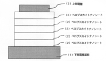
- FIG. 3 is a structural schematic diagram of a thin film element constituted by a perovskite nanosheet thin film shown in Examples 1 to 4. It is a figure which shows the result of having evaluated the cross-sectional structure of the thin film by high-resolution transmission electron microscope observation with respect to the thin film which laminated
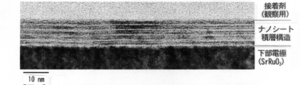
- FIG. It is a figure which shows the result of having evaluated the cross-sectional structure of the thin film by high-resolution transmission electron microscope observation with respect to the thin film which laminated
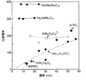
- FIG. FIG. 6 is a diagram comparing the film thickness dependence of the relative dielectric constant of the perovskite nanosheet thin film shown in Examples 1 to 4 and a typical high dielectric constant oxide material.
- the present inventors discovered the high dielectric properties of perovskite structure oxides, discovered room temperature solution processes suitable for the production of high dielectric thin films, and further applied these findings to obtain the present invention. It came.
- the present invention has the characteristics as described above, and an embodiment thereof will be described below.
- FIG. 1 is a diagram schematically illustrating a cross-sectional structure of a high dielectric thin film made of a high dielectric nanosheet-like perovskite oxide according to an embodiment of the present invention.
- (1) is a lower electrode substrate made of atomic flat epitaxial SrRuO 3 (hereinafter simply referred to as “substrate (1)”), and (2) is a high electrode formed on the substrate (1).
- FIG. 1 shows an example of forming a multi-layer structure obtained by laminating a perovskite nanosheets (2) on the lower electrode substrate (1) made of SrRuO 3.
- the lower electrode substrate (1) is not limited to, for example, an atomic flat epitaxial substrate, but a metal electrode such as gold, platinum, copper, or aluminum, or a conductivity such as Nb-doped SrTiO 3 .
- a perovskite nanosheet thin film may be similarly disposed on a perovskite substrate, a transparent oxide electrode such as ITO, Ga-doped ZnO, or Nb-doped TiO 2, or another type of substrate such as Si, glass, or plastic.
- the upper electrode (3) may be of various types as with the lower electrode substrate (1).
- Perovskite nanosheets (2) (for example, Ca 2 NaNb 3 O 13 ), which are the constituent layers of high-dielectric thin films, are peeled from layered perovskite oxide to one layer, which is the basic minimum unit of crystal structure, by soft chemical treatment. It is a nanomaterial having two-dimensional anisotropy obtained by doing so.
- the high dielectric element of the present invention is mainly composed of such a high dielectric perovskite nanosheet or a laminate thereof.
- the perovskite nanosheet preferably has a thickness of 10 nm or less (corresponding to several atoms). ), May have a particle size of 100 nm to 1000 ⁇ m in lateral size.
- Such a perovskite nanosheet is obtained by exfoliation from a layered perovskite oxide, and various layered perovskite oxides may be used at this time.
- a highly functional dielectric block is preferable. Examples thereof include those represented by the composition formulas described in Tables 1 to 4 including NbO 6 octahedron, TaO 6 octahedron or TiO 6 octahedron.
- the treatment for peeling can be called soft chemical treatment, and this soft chemical treatment is a treatment combining acid treatment and colloidalization treatment. That is, when an aqueous solution of acid such as hydrochloric acid is brought into contact with a perovskite oxide powder or single crystal having a layered structure, the product is filtered, washed, and dried, all alkali metal ions present between the layers before the treatment are all removed. A hydrogen-type substance is obtained by replacing hydrogen ions. Next, when the obtained hydrogen-type substance is placed in an aqueous solution of amine or the like and stirred, it is colloidalized. At this time, the layers constituting the layered structure are peeled up one by one. The film thickness can be controlled in the nm range.
- Nanosheet peeling by soft chemical treatment has become a well-known technique since the inventors of the present application previously invented and filed patent applications and papers. Therefore, although it is considered that there is no need to give a general explanation in detail in the present application, for example, refer to Patent Documents 1 and 2 if necessary.
- the peeled perovskite nanosheet can be formed into a high dielectric thin film using the Langmuir-Blodgett method (hereinafter, simply referred to as “LB method”) already proposed by the present inventors.
- the LB method is a method known as a method for forming a clay mineral or an organic nano thin film. By using an amphiphilic molecule, an associated film is formed on the air-water interface, and this is transferred to a substrate. This is a method for producing a uniform monolayer film.
- perovskite nanosheets when a low concentration of perovskite nanosheet sol solution is used, the nanosheets are adsorbed on the air-water interface without using amphiphilic cationic molecules, and further, the barrier causes the air-water interface.
- the nanosheets adsorbed on the substrate By gathering together the nanosheets adsorbed on the substrate, it becomes possible to produce a high-quality monolayer film in which the perovskite nanosheets are densely coated on the substrate surface without gaps. Then, by repeating the above LB method and laminating perovskite nanosheets, a high dielectric thin film having a multilayer structure is provided. See Non-Patent Document 1 for details of the LB method.
- a high dielectric thin film made of the same perovskite nanosheet can be formed by the alternating self-organized lamination technique that the present inventors have already proposed as Patent Document 1 and Patent Document 2. it can.
- polyethyleneimine (PEI) described in the examples polyethyleneimine (PEI) described in the examples, polydiallyldimethylammonium chloride (PDDA) having the same cationic property, polyallylamine hydrochloride (PAH) and the like are suitable.
- PKI polyethyleneimine
- PDDA polydiallyldimethylammonium chloride
- PAH polyallylamine hydrochloride
- the organic polymer an inorganic polymer having a positive charge and an inorganic compound containing polynuclear hydroxide ions are used. You can also
- the perovskite nanosheet is coated on the substrate surface without gaps, and the overlap between the perovskite nanosheets is removed or reduced.
- a method for forming a single layer film is provided.
- the means for coating the perovskite nanosheet without any gaps on the substrate surface is a colloid in which the flake particles are suspended after the substrate is immersed in the cationic organic polymer solution to adsorb the organic polymer on the substrate surface.
- a method of forming a single layer characterized by a process in which nanosheets are self-organizedly adsorbed on a substrate by electrostatic interaction by immersing them in a solution, and overlapping portions of the perovskite nanosheets
- An example of the method for forming a monolayer film is characterized in that the removing and reducing treatment means is performed by ultrasonic treatment in an alkaline aqueous solution.
- an inorganic high dielectric thin film can be formed by removing the organic polymer by irradiating with ultraviolet rays.
- the ultraviolet irradiation at this time may be ultraviolet irradiation including a wavelength of a band gap or less that activates the photocatalytic organic matter decomposition reaction of the layered perovskite oxide, and more preferably 12 using a xenon light source of 1 mW / cm 2 or more. It is desirable to irradiate more than an hour.
- the inorganic high dielectric thin film can be processed by low-temperature heating, and the same effect as ultraviolet irradiation can be achieved.
- the heat treatment at this time may be 800 ° C. or lower, which is the heat stable temperature of the layered perovskite oxide, and heat treatment is performed at a temperature of 300 ° C. or lower for resin substrates such as epoxy and other substrates having a low heat resistance temperature. Is desirable.
- a method of manufacturing a high dielectric thin film or an element thereof including the above method as at least a part of the process is realized.
- a layered perovskite oxide (KCa 2 NaNb 4 O 13 , KCa 2 Na 2 Nb 5 O 16 ) is used as a starting material, and perovskite nanosheets (Ca 2 NaNb 4 O 13 , Ca 2 Na 2 Nb 5 O 16 ), and as shown in FIG. 1, a high dielectric having a multilayer structure on the atomic flat epitaxial SrRuO 3 substrate by a LB method or an alternating self-organized lamination technique via a cationic polymer A thin film is produced.
- the present invention is not limited to the following examples.
- a perovskite nanosheet (Ca 2 NaNb 4 O 13 ) was prepared using a layered perovskite oxide (for example, KCa 2 NaNb 4 O 13 ) as a starting material, and this is the lower electrode substrate as shown in FIG.
- a high dielectric thin film made of the perovskite nanosheet (2) was produced by the LB method as follows.
- the layered perovskite oxide KCa 2 NaNb 4 O 13 is obtained by mixing at a ratio of KCa 2 Nb 3 O 10 and NaNbO 3 1: 1 and firing at 1273 K for 24 hours.
- the resulting powder 5g was acid-treated in nitric acid solution 200 cm 3 of 5 N at room temperature, to obtain a hydrogen-exchange layered perovskite oxide HCa 2 NaNb 4 O 13 ⁇ 1.5H 2 O, then each of the tetrabutyl ammonium hydroxide in hydrogen exchange type layered perovskite oxide 0.4 g (hereinafter referred to as TBAOH) stirred for 7 days at room temperature by adding an aqueous solution 100 cm 3, by reacting the composition formula Ca 2 NaNb 4 O
- a milky white sol solution was prepared in which rectangular nanosheets (2) having a thickness of 13 and having a thickness of about 2 nm and a lateral size of about 10 ⁇ m were dispersed.
- Each perovskite nanosheet / sol solution 8 cm 3 was dispersed in ultrapure water in a 1 dm 3 volumetric flask. The dispersion was allowed to stand for about half a day to about 1 day, and then the dispersion was spread on an LB trough thoroughly washed with acetone, and then waited for 30 minutes so that the stability of the water surface and the temperature of the lower layer solution became constant. Thereafter, the substrate (1) prepared above is set in the LB film forming apparatus, and a series of operations shown below is performed on the perovskite nanosheet as one cycle, and this cycle is repeated to laminate the perovskite nanosheet. A high dielectric thin film having a multilayer structure is provided.
- the thin film having the multilayer structure thus obtained is irradiated with ultraviolet rays using a xenon light source (1 mW / cm 2 , 72 hours), and the TBAOH used as a release agent is decomposed and removed using the photocatalytic reaction of the perovskite nanosheet. A thin film was obtained.
- FIG. 2 shows the result of evaluating the cross-sectional structure of the thin film by observation with a high-resolution transmission electron microscope, with respect to the multilayer structure in which five layers of Ca 2 NaNb 4 O 13 prepared as described above are laminated.
- a laminated structure in which nanosheets were accumulated in parallel at the atomic level on the substrate was confirmed, and each layer had a thickness of about 2 nm and had a multilayer structure in which five layers were laminated. From this, it was confirmed that a high-quality multilayer structure film in which the nanosheet monolayer film was alternately laminated while maintaining the denseness and smoothness was realized.
- Table 5 shows a thin film in which a gold dot electrode is formed as an upper electrode with respect to a high dielectric thin film having a multilayer structure in which three layers, five layers, and ten layers of Ca 2 NaNb 4 O 13 are produced.
- the dielectric constant and leakage current density in an element, that is, a high dielectric element are summarized.
- the leakage current density is measured by a Keithley semiconductor parameter analyzer (4200-SCS) at an applied voltage of +1 V.
- the relative dielectric constant is measured by a high precision LCR meter (4284A) manufactured by Agilent Technologies. It is the result of measuring the capacitance at 10 kHz and calculating the relative dielectric constant.
- the leakage current characteristics of perovskite nanosheets to high dielectric thin films show good insulation characteristics of 10 ⁇ 8 A / cm 2 or less in spite of the extremely thin film thickness of 6 to 20 nm. It was.
- the leakage current when compared with the existing material with a film thickness of 10 nm is extremely excellent insulation characteristics in which the leakage current is suppressed by about 4 digits compared to the existing perovskite oxide thin film (Ba, Sr) TiO 3. Indicates.
- the relative dielectric constant of the perovskite nanosheet showed a high relative dielectric constant of 300 or more regardless of the number of stacked layers. From the above, it was possible to produce a high dielectric thin film that simultaneously realizes stable high dielectric properties and insulating properties regardless of the nanoscale film thickness.
- a perovskite nanosheet Ca 2 NaNb 4 O 13 was prepared using the layered perovskite oxide KCa 2 NaNb 4 O 13 as a starting material, and as shown in FIG. SrRuO 3 on the substrate (1), a high dielectric thin film by alternately self-organization lamination techniques the perovskite nanosheet (2) was prepared as follows.
- Example 2 In the same manner as in Example 1, the layered perovskite oxide KKCa 2 NaNb 4 O 13 was peeled off as a single layer, a rectangle whose composition formula was represented by KCa 2 NaNb 4 O 13 was about 2 nm, and the lateral size was about 10 ⁇ m. A milky white sol solution in which the nanosheets (2) were dispersed was prepared.
- FIG. 1 shows the result of repeating this cycle three times.
- Soak in a PEI solution for 20 minutes as the polycation solution [2] Wash thoroughly with Milli-Q pure water [3] Soak in one of the stirred nanosheet sol solutions [4] 20 minutes elapsed Later, it is sufficiently washed with Milli-Q pure water.
- the obtained thin film is immersed in a TBAOH aqueous solution having a pH of 11, it is subjected to ultrasonic treatment for 20 minutes in an ultrasonic washing tank (Branson, 42 kHz, 90 W).
- the thin film having the superlattice structure thus obtained is irradiated with ultraviolet light using a xenon light source (1 mW / cm 2 , 72 hours), and the organic polymer is decomposed and removed using the photocatalytic reaction of the perovskite nanosheet.
- Example 2 For the high dielectric thin film having a multilayer structure in which three layers, five layers, and ten layers of Ca 2 NaNb 4 O 13 were produced as described above, the relative permittivity and the dielectric constant were determined by the same method and measurement conditions as in Example 1. When the leakage current density was evaluated, the same results as in Table 5 were obtained. That is, in Example 2, the effectiveness of the present invention was proved by an element manufacturing method different from that in Example 1.
- a perovskite nanosheet (Ca 2 Na 2 Nb 5 O 16 ) was prepared using a layered perovskite oxide (for example, KCa 2 Na 2 Nb 5 O 16 ) as a starting material, and as shown in FIG.
- a layered perovskite oxide for example, KCa 2 Na 2 Nb 5 O 16
- a high dielectric thin film made of the perovskite nanosheet (2) was produced by the LB method as follows.
- the layered perovskite oxide KCa 2 Na 2 Nb 5 O 16 was obtained by mixing at a ratio of KCa 2 NaNb 4 O 13 and NaNbO 3 1: 1 and firing at 1473 K for 24 hours.
- the resulting powder 5g was acid-treated in nitric acid solution 200 cm 3 of 5 N at room temperature, to obtain a hydrogen-exchange layered perovskite oxide HCa 2 Na 2 Nb 5 O 16 ⁇ 1.5H 2 O, then each of the hydrogen-exchange layered perovskite oxide 0.4g tetrabutylammonium hydroxide (hereinafter referred to as TBAOH) stirred for 7 days at room temperature by adding an aqueous solution 100 cm 3, by reacting the composition formula Ca 2 Na A milky white sol solution in which rectangular nanosheets (2) having a thickness represented by 2 Nb 5 O 16 of about 2.5 nm and a lateral size of about 5 ⁇ m were dispersed was prepared.
- TBAOH tetrabuty
- Each perovskite nanosheet / sol solution 8 cm 3 was dispersed in ultrapure water in a 1 dm 3 volumetric flask. This dispersion solution is allowed to stand for about a half day to a day, and then the dispersion solution is spread on an LB trough thoroughly washed with acetone, and then waits for 30 minutes so that the stability of the water surface and the temperature of the lower layer solution become constant. Thereafter, the substrate (1) prepared above is set in the LB film forming apparatus, and a series of operations shown below is performed on the perovskite nanosheet as one cycle, and this cycle is repeated to laminate the perovskite nanosheet. A high dielectric thin film having a multilayer structure is provided.
- the thin film having the multilayer structure thus obtained is irradiated with ultraviolet rays using a xenon light source (1 mW / cm 2 , 72 hours), and the TBAOH used as a release agent is decomposed and removed using the photocatalytic reaction of the perovskite nanosheet. A thin film was obtained.
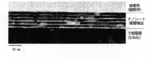
- FIG. 3 shows the results of evaluating the cross-sectional structure of the thin film by high-resolution transmission electron microscope observation with respect to the multilayer structure in which five layers of Ca 2 Na 2 Nb 5 O 16 prepared as described above are laminated.
- a laminated structure in which nanosheets were accumulated in parallel at the atomic level on the substrate was confirmed, and each layer had a thickness of about 2.5 nm and had a multilayer structure in which five layers were laminated. From this, it was confirmed that a high-quality multilayer structure film in which the nanosheet monolayer film was alternately laminated while maintaining the denseness and smoothness was realized.
- Table 6 shows that a gold dot electrode is formed as an upper electrode for the high dielectric thin film having a multilayer structure in which three layers, five layers, and ten layers of Ca 2 Na 2 Nb 5 O 16 are produced as described above.
- the relative dielectric constant and leakage current density of the thin film element, that is, the high dielectric element are summarized.
- the leakage current density is measured by a Keithley semiconductor parameter analyzer (4200-SCS) at an applied voltage of +1 V.
- the relative dielectric constant is measured by a high precision LCR meter (4284A) manufactured by Agilent Technologies. It is the result of measuring the capacitance at 10 kHz and calculating the relative dielectric constant.
- the leakage current characteristics from the perovskite nanosheet to the high dielectric thin film showed good insulation characteristics of 10 ⁇ 7 A / cm 2 or less in spite of the extremely thin film thickness of 5 to 25 nm. It was.
- the leakage current when compared with the existing material with a film thickness of 12 nm is extremely excellent insulation characteristics in which the leakage current is suppressed by about 3 digits compared to the existing perovskite oxide thin film (Ba, Sr) TiO 3. Indicates.
- the relative dielectric constant of the perovskite nanosheet showed a high relative dielectric constant of 300 or more regardless of the number of stacked layers.
- Example 3 the effectiveness of the present invention was demonstrated using a material different from those in Examples 1 and 2.
- perovskite nanosheets Ca 2 NaNb 4 O 13 and Ca 2 Na 2 Nb 5 O 16 were prepared using layered perovskite oxides KCa 2 NaNb 4 O 13 and KCa 2 Na 2 Nb 5 O 16 as starting materials.
- a high dielectric thin film made of the perovskite nanosheet (2) was produced on the Pt substrate (1) as the lower electrode substrate by the LB method as follows.
- the perovskite nanosheets Ca 2 NaNb 4 O 13 and Ca 2 Na 2 Nb 5 O 16 are obtained by using the layered perovskite oxides KCa 2 NaNb 4 O 13 and KCa 2 Na 2 Nb 5 O 16 as starting materials. The same method was used.
- the surface was cleaned by irradiating the Pt substrate (1) used as the lower electrode with ultraviolet rays in an ozone atmosphere.
- the thin film having the multilayer structure thus obtained is irradiated with ultraviolet rays using a xenon light source (1 mW / cm 2 , 72 hours), and the TBAOH used as a release agent is decomposed and removed using the photocatalytic reaction of the perovskite nanosheet. A thin film was obtained.
- Table 7 summarizes the relative permittivity and leakage current density in the five-layer laminated film of Ca 2 NaNb 4 O 13 and Ca 2 Na 2 Nb 5 O 16 produced as described above.
- the relative permittivity and the leakage current density were evaluated by the same method and measurement conditions as in Examples 1 to 3
- the Ca 2 NaNb 4 O 13 results were the same as in Table 5 and the results were Ca 2 Na 2 Nb 5 O 16.
- the same results as in Table 6 were obtained. That is, in Example 4, the effectiveness of the present invention was demonstrated with an element structure different from those in Examples 1 to 3.
- FIG. 4 is the result of plotting the film thickness dependence of the relative dielectric constant for the high dielectric thin film composed of Ca 2 NaNb 4 O 13 and Ca 2 Na 2 Nb 5 O 16 shown in Examples 1 to 4.
- the film thickness dependence of the relative dielectric constant of a typical high dielectric constant oxide material is shown for comparison.
- a conventional perovskite-based oxide for example, (Ba, Sr) TiO 3
- the thickness is reduced to the nano level with the aim of increasing the capacity, the relative permittivity decreases
- the perovskite nanosheet thin film of the present invention There was no significant size effect, and a high relative dielectric constant of 200 or more was maintained even in a thin film of about 5 to 10 nm.
- the perovskite nanosheet thin film of the present invention has an excellent relative dielectric constant that greatly surpasses the existing high dielectric constant oxide materials in the thin film region of the 10 nm level. Therefore, according to the present invention, there is an epoch-making effect that a size-free high dielectric constant characteristic that simultaneously realizes a high dielectric constant and a good insulating characteristic can be obtained even in the nano region.
- the perovskite nanosheet thin film of the present invention has an excellent relative dielectric constant that greatly exceeds the existing high dielectric constant oxide materials in a thin film region having a thickness of 50 nm or less.
- the perovskite nanosheet thin film is also attached to the upper electrode substrate based on the methods of Examples 1 to 4 above, and the both can be multilayered together. This is a category.
- the present invention has been described with reference to an example in which a multilayer structure of perovskite nanosheets is formed on an atomic flat epitaxial SrRuO 3 substrate and Pt and applied to a high dielectric thin film and a high dielectric element.
- the high dielectric element according to the invention can be used alone as a thin film capacitor, and can also be used as a multilayer capacitor, a high frequency device, a DRAM memory, a gate insulator for a transistor, and the like, and has the same excellent effect.
- the present invention by utilizing the unique nanophysical properties and high structure and structure controllability possessed by the perovskite nanosheet, a high dielectric constant and good insulating properties can be realized at the same time in the nano region. Can do.
- Perovskite nanosheets can be fabricated by using soft chemical reactions such as self-organization at room temperature, so it is possible to avoid problems such as substrate interface deterioration and compositional deviation due to thermal annealing in the conventional manufacturing process. Fusion with various materials is possible.
- an epoxy resin substrate has a heat resistance as low as about 300 ° C., and it has been impossible to mount a capacitor.
- the perovskite nanosheet of the present invention it is possible to form a high dielectric thin film or a capacitor. Implementation is possible.
- the present invention it is possible to realize a low-cost, low-environment process that does not require a large vacuum apparatus or an expensive film forming apparatus, which is the mainstream of conventional dielectric thin film processes. Therefore, if the high dielectric constant nanomaterial of the present invention is used in a technical field such as multilayer capacitors, high frequency devices, IT materials, nanoelectronics, etc., where the high dielectric constant material is a key component, it is extremely useful. It is concluded that there is.
- the unique high dielectric properties and high structural controllability of the perovskite structure oxide can be utilized, and high dielectric properties can be realized.
- the unique high dielectric properties and excellent insulating properties of the layered perovskite structure in which at least four NbO 6 octahedrons, TaO 6 octahedrons or TiO 6 octahedrons are included in the unit cell, High dielectric properties and excellent insulation properties can be realized at the same time.
- perovskite oxide containing NbO 6 octahedron, TaO 6 octahedron or TiO 6 octahedron known as a high dielectric material as a basic block is extracted as a single nanosheet, and can be artificially reconstructed.
- a nanosheet-like perovskite oxide containing NbO 6 octahedron, TaO 6 octahedron or TiO 6 octahedron can be stably extracted as a simple substance, and has a higher dielectric constant than a conventional perovskite. It is possible to manufacture and design a high-dielectric thin film having
- nanosheet-like perovskite oxides that are weakly self-supporting can be easily handled by being held on the electrode substrate, and the productivity of devices using a high dielectric thin film can be ensured.
- a dielectric element can be provided.
- a body element can be provided.
- inorganic high-dielectric elements from which organic substances have been removed can be manufactured stably and simply by low-temperature heating, thus eliminating problems such as substrate interface deterioration and compositional deviation associated with the heat treatment process of conventional element manufacturing processes.
- a high-performance high dielectric element can be provided.
- High dielectric thin films are used in all kinds of electronic equipment such as multilayer capacitors, high frequency devices, DRAM memories, and gate insulators for transistors, and are surpassing R & D in industry, government, and academia around the world for practical application.
- the newly developed nanomaterials are (1) capable of functioning with the smallest thin film among conventional materials and simultaneously realizing a high dielectric constant and good insulating properties, and (2) room temperature and low cost.
- All the problems associated with conventional thermal annealing have been eliminated by realizing the room temperature process, and (4) Resins that have been difficult to mount in the past.
Landscapes
- Chemical & Material Sciences (AREA)
- Engineering & Computer Science (AREA)
- Organic Chemistry (AREA)
- Ceramic Engineering (AREA)
- Manufacturing & Machinery (AREA)
- Inorganic Chemistry (AREA)
- Materials Engineering (AREA)
- Structural Engineering (AREA)
- Nanotechnology (AREA)
- Power Engineering (AREA)
- Crystallography & Structural Chemistry (AREA)
- General Physics & Mathematics (AREA)
- Condensed Matter Physics & Semiconductors (AREA)
- Composite Materials (AREA)
- Physics & Mathematics (AREA)
- Microelectronics & Electronic Packaging (AREA)
- Inorganic Compounds Of Heavy Metals (AREA)
- Semiconductor Memories (AREA)
- Thin Film Transistor (AREA)
- Insulated Gate Type Field-Effect Transistor (AREA)
- Laminated Bodies (AREA)
- Semiconductor Integrated Circuits (AREA)
- Ceramic Capacitors (AREA)
- Inorganic Insulating Materials (AREA)
Abstract
Description
ここで、前記ナノシートの横サイズが10nm~1000μmであってよい。
また、前記ナノシートが以下の組成式で表される層状酸化物のいずれか又はその水和物を剥離して得られたものであってよい:
組成式A[Ca2Nan-3NbnO3n+1-d]、A[(Ca1-xSrx)2Nan-3NbnO3n+1-d]、あるいはA[Mn-1A’n-3M’nO3n+1-d](A、A’は、H、Li、Na、K、Rb、Csから選ばれる少なくとも1種であり;Mは、Sr、Ba、Pb、Biあるいは希土類元素La、Ce、Pr、Sm、Eu、Gd、Tb、Dy、Ho、Er、Tm、Yb、Luから選ばれる少なくとも1種であり;M’は、Ti、Mg、Mn、Zn、Nb、Taから選ばれる少なくとも1種であり;x=0-1;n=3-8;d=0-2)。
また、前記ナノシートが以下の組成式で表されるペロブスカイト酸化物であってよい:
組成式[Ca2Nan-3NbnO3n+1-d]、[(Ca1-xSrx)2Nan-3NbnO3n+1-d]、あるいは[Mn-1A’n-3M’nO3n+1-d](A’は、H、Li、Na、K、Rb、Csから選ばれる少なくとも1種であり;Mは、Sr、Ba、Pb、Biあるいは希土類元素La、Ce、Pr、Sm、Eu、Gd、Tb、Dy、Ho、Er、Tm、Yb、Luから選ばれる少なくとも1種であり;M’は、Ti、Mg、Mn、Zn、Nb、Taから選ばれる少なくとも1種であり;x=0-1;n=3-8;d=0-2)。
また、高誘電性ナノシート積層体は厚さが1nm~100nmであってよい。
本発明の他の側面によれば、電極基板に上記いずれかの高誘電性ナノシート積層体を付着させた高誘電体素子が与えられる。
本発明の更に他の側面によれば、第1の電極基板と第2の電極基板の間に上記いずれかの高誘電性ナノシート積層体を設けた高誘電体素子が与えられる。
本発明の更に他の側面によれば、前記第1及び第2の電極基板の少なくとも一方の電極基板に上記いずれかの高誘電性ナノシート積層体を付着させ、前記高誘電性ナノシート積層体を中間にして前記第1及び第2の電極基板を配置する、前記高誘電体素子の製造方法が与えられる。
本発明の更に他の側面によれば、Langmuir-Blodgett法により前記酸化物を基板表面上に緻密かつ隙間なく被覆した単層膜を形成して前記単層膜を前記電極基板に付着する工程を繰り返すことにより前記高誘電性ナノシート積層体を作製する、前記高誘電体素子の製造方法が与えられる。
本発明の更に他の側面によれば、前記電極基板をカチオン性有機ポリマー溶液中に浸漬して、その基板表面に有機ポリマーを吸着させた後、前記ナノシートが懸濁したコロイド溶液中に浸漬することにより、前記ナノシートを静電的相互作用によって、前記ポリマー上に吸着させ、前記高誘電性ナノシート積層体を作製する、前記高誘電体素子の製造方法が与えられる。
ここで、前記ナノシートを静電的相互作用によって前記電極基板上に吸着させる前記工程において、超音波を付与して前記ナノシート同士の重複部分を除去してよい。
また、前記高誘電性ナノシート積層体を生成した後に、紫外線を照射して前記有機ポリマーを除去してよい。
また、前記高誘電性ナノシート積層体を生成した後に、加熱により前記有機ポリマーを除去してよい。


LB法とは、粘土鉱物あるいは有機ナノ薄膜の製膜法として知られる手法であり、両親媒性分子を利用して気-水界面上において会合膜を形成し、これを基板に転写させることで、均一なモノレイヤー膜を作製する手法である。ペロブスカイトナノシートの場合には、低濃度のペロブスカイトナノシート・ゾル溶液を用いると、両親媒性であるカチオン性分子を用いることなく、気-水界面にナノシートが吸着し、さらにバリヤにより、気-水界面に吸着したナノシートを寄せ集めることで、ペロブスカイトナノシートが基板表面上に緻密かつ隙間なく被覆した高品位単層膜の製造が可能になる。
そして、上記のLB法を繰り返し行い、ペロブスカイトナノシートを積層することで、多層構造を有する高誘電体薄膜が提供される。LB法の詳細については非特許文献1を参照されたい。
実際の操作としては、基板を(1)有機ポリカチオン溶液に浸漬→(2)純水で洗浄→(3)ペロブスカイトナノシート・ゾル溶液に浸漬→(4)純水で洗浄する、という一連の操作を1サイクルとして、これを少なくとも2種類のペロブスカイトナノシートに対して必要回数分反復する。有機ポリカチオンとしては、実施例記載のポリエチレンイミン(PEI)、さらに同様なカチオン性を有するポリジアリルジメチルアンモニウム塩化物(PDDA)、塩酸ポリアリルアミン(PAH)などが適当である。また、交互積層に際しては、基板表面に正電荷を導入することができれば基本的に問題なく、有機ポリマーの代わりに、正電荷を持つ無機高分子、多核水酸化物イオンを含む無機化合物を使用することもできる。
そして、上記の方法を繰り返し行い、ペロブスカイトナノシートを積層することで、多層構造を有する高誘電体薄膜が提供される。
たとえば以下の実施例に示した形態では、層状ペロブスカイト酸化物(KCa2NaNb4O13、KCa2Na2Nb5O16)を出発原料に、ペロブスカイトナノシート(Ca2NaNb4O13、Ca2Na2Nb5O16)を作製し、図1に示したように、原子平坦性エピタキシャルSrRuO3基板上にカチオン性ポリマーを介してLB法あるいは交互自己組織化積層技術により多層構造を有する高誘電体薄膜を作製している。
なお、本発明は以下の実施例によって限定されるものでないことは言うまでもない。
[1]圧縮速度0.5mm/分でバリヤを移動させて表面を圧縮することにより、気-水界面上に分散した一方の種類のペロブスカイトナノシートを寄せ集め、一定圧力になった後30分間静置する。このようにして、気-水界面にてペロブスカイトナノシートを並置一体化したモノレイヤー膜を形成する。
[2]引き上げ速度0.8mm/分で基板(1)を垂直に引き上げて前記モノレイヤー膜を基板に付着させることで、一方の種類のペロブスカイトナノシートが緻密にパックされた薄膜を得る。

[1]上記ポリカチオン溶液としてPEI溶液に20分間浸漬する
[2]Milli-Q純水で充分に洗浄する
[3]撹拌した上記ナノシートゾル溶液の一方の中に浸漬する
[4]20分経過後にMilli-Q純水で充分に洗浄する
[5]得られた薄膜をpH11のTBAOH水溶液中に浸漬しながら、超音波洗浄槽(ブランソン製、42kHz、90W)にて20分間超音波処理する。
[1]圧縮速度0.5mm/分でバリヤを移動させて表面を圧縮することにより、気-水界面上に分散した一方の種類のペロブスカイトナノシートを寄せ集め、一定圧力になった後30分間静置する。このようにして、気-水界面にてペロブスカイトナノシートを並置一体化したモノレイヤー膜を形成する。
[2]引き上げ速度0.8mm/分で基板(1)を垂直に引き上げて前記モノレイヤー膜を基板に付着させることで、一方の種類のペロブスカイトナノシートが緻密にパックされた薄膜を得る。

[1]圧縮速度0.5mm/分でバリヤを移動させて表面を圧縮することにより、気-水界面上に分散したペロブスカイトナノシートを寄せ集め、一定圧力になった後30分間静置する。このようにして、気-水界面にてペロブスカイトナノシートを並置一体化したモノレイヤー膜を形成する。
[2]引き上げ速度0.8mm/分で基板(1)を垂直に引き上げ、前記モノレイヤー膜が基板に付着し、ペロブスカイトナノシートが緻密にパックされた薄膜を得る。

なお、高誘電体薄膜の多層膜化するに当たり、上部電極基板に対しても、上記実施例1から4の手法に基づき、ペロブスカイトナノシート薄膜を付着させ、両者を併せて多層化することも本発明の範疇である。
以上の実施の形態においては、原子平坦性エピタキシャルSrRuO3基板、Pt上にペロブスカイトナノシートの多層構造を形成して高誘電体薄膜、高誘電体素子に適用する例によって本発明を説明したが、本発明に係わる高誘電体素子は、単独で薄膜コンデンサとしても利用でき、また、積層コンデンサ、高周波デバイス、DRAMメモリ、トランジスタ用ゲート絶縁体などにも利用でき、同様の優れた効果を奏する。
また、従来の高誘電体薄膜プロセスと異なり、高温でのアニール等が不要な、室温での溶液プロセスが可能になったため、従来の素子製造行程における基板界面劣化、組成ズレなどの問題を回避して、高性能の高誘電体素子を提供することができる。
Claims (13)
- NbO6八面体、TaO6八面体もしくはTiO6八面体を単位格子内に少なくとも4個内包したペロブスカイト構造を有する酸化物の厚み10nm以下のナノシートを積層した、高誘電性ナノシート積層体。
- 前記ナノシートの横サイズが10nm~1000μmである、請求項1に記載の高誘電性ナノシート積層体。
- 前記ナノシートが以下の組成式で表される層状酸化物のいずれか又はその水和物を剥離して得られたものである、請求項1または2に記載の高誘電性ナノシート積層体。
組成式A[Ca2Nan-3NbnO3n+1-d]、A[(Ca1-xSrx)2Nan-3NbnO3n+1-d]、あるいはA[Mn-1A’n-3M’nO3n+1-d](A、A’は、H、Li、Na、K、Rb、Csから選ばれる少なくとも1種であり;Mは、Sr、Ba、Pb、Biあるいは希土類元素La、Ce、Pr、Sm、Eu、Gd、Tb、Dy、Ho、Er、Tm、Yb、Luから選ばれる少なくとも1種であり;M’は、Ti、Mg、Mn、Zn、Nb、Taから選ばれる少なくとも1種であり;x=0-1;n=3-8;d=0-2)。 - 前記ナノシートが以下の組成式で表されるペロブスカイト酸化物である、請求項1から3のいずれかに記載の高誘電性ナノシート積層体。
組成式[Ca2Nan-3NbnO3n+1-d]、[(Ca1-xSrx)2Nan-3NbnO3n+1-d]、あるいは[Mn-1A’n-3M’nO3n+1-d](A’は、H、Li、Na、K、Rb、Csから選ばれる少なくとも1種であり;Mは、Sr、Ba、Pb、Biあるいは希土類元素La、Ce、Pr、Sm、Eu、Gd、Tb、Dy、Ho、Er、Tm、Yb、Luから選ばれる少なくとも1種であり;M’は、Ti、Mg、Mn、Zn、Nb、Taから選ばれる少なくとも1種であり;x=0-1;n=3-8;d=0-2)。 - 厚さが1nm~100nmである、請求項1から4のいずれかに記載の高誘電性ナノシート積層体。
- 電極基板に請求項1から5のいずれかに記載の高誘電性ナノシート積層体を付着させた高誘電体素子。
- 第1の電極基板と第2の電極基板の間に請求項1から5のいずれかに記載の高誘電性ナノシート積層体を設けた高誘電体素子。
- 前記第1及び第2の電極基板の少なくとも一方の電極基板に請求項1から5のいずれかに記載の高誘電性ナノシート積層体を付着させ、前記高誘電性ナノシート積層体を中間にして前記第1及び第2の電極基板を配置する、請求項7に記載の高誘電体素子の製造方法。
- Langmuir-Blodgett法により前記酸化物を基板表面上に緻密かつ隙間なく被覆した単層膜を形成して前記単層膜を前記電極基板に付着する工程を繰り返すことにより、前記高誘電性ナノシート積層体を作製する、請求項8に記載の高誘電体素子の製造方法。
- 前記電極基板をカチオン性有機ポリマー溶液中に浸漬して、その基板表面に有機ポリマーを吸着させた後、前記ナノシートが懸濁したコロイド溶液中に浸漬することにより、前記ナノシートを静電的相互作用によって、前記ポリマー上に吸着させ、前記高誘電性ナノシート積層体を作製する、請求項8に記載の高誘電体素子の製造方法。
- 前記ナノシートを静電的相互作用によって前記電極基板上に吸着させる前記工程において、超音波を付与して前記ナノシート同士の重複部分を除去する、請求項10に記載の高誘電体素子の製造方法。
- 前記高誘電性ナノシート積層体を生成した後に、紫外線を照射して前記有機ポリマーを除去する、請求項10または11に記載の高誘電体素子の製造方法。
- 前記高誘電性ナノシート積層体を生成した後に、加熱により前記有機ポリマーを除去する、請求項10または11に記載の高誘電体素子の製造方法。
Priority Applications (2)
| Application Number | Priority Date | Filing Date | Title |
|---|---|---|---|
| KR1020137029964A KR101575668B1 (ko) | 2011-05-19 | 2012-05-18 | 고유전성 나노시트 적층체 및 고유전체 소자와 그 제조방법 |
| US14/118,354 US9082551B2 (en) | 2011-05-19 | 2012-05-18 | High dielectric nanosheet laminate, high dielectric element and method for producing the same |
Applications Claiming Priority (2)
| Application Number | Priority Date | Filing Date | Title |
|---|---|---|---|
| JP2011-112462 | 2011-05-19 | ||
| JP2011112462A JP5885150B2 (ja) | 2011-05-19 | 2011-05-19 | 高誘電性ナノシート積層体、高誘電性ナノシート積層体、高誘電体素子、および高誘電体薄膜素子の製造方法 |
Publications (1)
| Publication Number | Publication Date |
|---|---|
| WO2012157740A1 true WO2012157740A1 (ja) | 2012-11-22 |
Family
ID=47177054
Family Applications (1)
| Application Number | Title | Priority Date | Filing Date |
|---|---|---|---|
| PCT/JP2012/062765 Ceased WO2012157740A1 (ja) | 2011-05-19 | 2012-05-18 | 高誘電性ナノシート積層体及び高誘電体素子とその製造方法 |
Country Status (4)
| Country | Link |
|---|---|
| US (1) | US9082551B2 (ja) |
| JP (1) | JP5885150B2 (ja) |
| KR (1) | KR101575668B1 (ja) |
| WO (1) | WO2012157740A1 (ja) |
Families Citing this family (22)
| Publication number | Priority date | Publication date | Assignee | Title |
|---|---|---|---|---|
| JP6103524B2 (ja) * | 2013-02-06 | 2017-03-29 | 国立研究開発法人物質・材料研究機構 | ホモロガス系列層状ペロブスカイト酸化物に基づくペロブスカイトナノシート、および、その用途 |
| US9685499B1 (en) | 2016-09-21 | 2017-06-20 | International Business Machines Corporation | Nanosheet capacitor |
| KR102469184B1 (ko) | 2017-10-27 | 2022-11-18 | 삼성전자주식회사 | 세라믹 전자 부품 및 그 제조 방법과 전자장치 |
| KR102469185B1 (ko) * | 2017-10-27 | 2022-11-18 | 삼성전자주식회사 | 세라믹 전자 부품 및 그 제조 방법과 전자장치 |
| CN110246689B (zh) * | 2018-03-09 | 2022-05-24 | 三星电子株式会社 | 陶瓷电介质及其制造方法和陶瓷电子组件及电子设备 |
| WO2019235385A1 (ja) | 2018-06-08 | 2019-12-12 | 国立研究開発法人産業技術総合研究所 | 脆性材料構造体 |
| US10991798B2 (en) | 2019-01-21 | 2021-04-27 | International Business Machines Corporation | Replacement sacrificial nanosheets having improved etch selectivity |
| KR20200099406A (ko) | 2019-02-14 | 2020-08-24 | 삼성전자주식회사 | 단결정 재료 및 그 제조 방법, 적층체, 세라믹 전자 부품 및 장치 |
| WO2020241714A1 (ja) | 2019-05-29 | 2020-12-03 | 国立研究開発法人産業技術総合研究所 | 含浸性を有する高密度脆性材料構造体 |
| KR102868047B1 (ko) * | 2019-10-10 | 2025-10-01 | 삼성전자주식회사 | 유전체 단층 박막, 이를 포함하는 커패시터 및 반도체 소자, 및 이의 제조방법 |
| US11342344B2 (en) * | 2019-11-05 | 2022-05-24 | Electronics And Telecommunications Research Institute | Memory device and method of manufacturing the same |
| KR102247789B1 (ko) | 2019-11-12 | 2021-05-03 | 울산과학기술원 | 유전 박막, 및 이를 포함하는 멤커패시터 |
| KR102259923B1 (ko) * | 2019-11-15 | 2021-06-02 | 광주과학기술원 | 유전박막, 이를 포함하는 멤커패시터, 이를 포함하는 셀 어레이, 및 그 제조 방법 |
| KR102794032B1 (ko) * | 2019-12-13 | 2025-04-11 | 삼성전자주식회사 | 커패시터 구조물 및 이를 포함하는 반도체 장치 |
| KR102831126B1 (ko) * | 2020-01-23 | 2025-07-04 | 삼성전자주식회사 | 이차원 물질로 이루어진 게이트 절연막을 포함하는 전계 효과 트랜지스터 |
| KR102752041B1 (ko) * | 2020-04-21 | 2025-01-09 | 삼성전자주식회사 | 고주파 동작 환경에서 사용될 수 있는 반도체 장치의 커패시터 |
| JP7431150B2 (ja) * | 2020-12-21 | 2024-02-14 | トヨタ自動車株式会社 | 被膜及び被膜を有する複合材料 |
| KR102417137B1 (ko) * | 2021-05-07 | 2022-07-06 | 한국과학기술연구원 | 유전 분산이 없는 칼슘 리튬 나이오베이트 유전체 조성물 및 그 제조방법 |
| CN113707769B (zh) * | 2021-08-24 | 2023-10-17 | 福州大学 | 基于转移印刷绝缘朗缪尔单层的高精度图案化led漏电流阻挡层及其制备方法 |
| JP2023087747A (ja) * | 2021-12-14 | 2023-06-26 | 国立研究開発法人物質・材料研究機構 | キャパシタ型蓄電デバイス |
| US20250006839A1 (en) * | 2023-06-28 | 2025-01-02 | Intel Corporation | P-type perovskite ferroelectric field effect transistor (fefet) devices |
| CN116960166B (zh) * | 2023-09-14 | 2023-11-24 | 泉州师范学院 | 一种高介电常数的纳米叠层介电薄膜及其制备方法 |
Citations (4)
| Publication number | Priority date | Publication date | Assignee | Title |
|---|---|---|---|---|
| JPH11139826A (ja) * | 1997-11-10 | 1999-05-25 | Agency Of Ind Science & Technol | 層間架橋構造を有する層状化合物の製造方法 |
| JP2000114093A (ja) * | 1998-09-29 | 2000-04-21 | Kyocera Corp | 誘電体薄膜およびセラミックコンデンサ |
| WO2008078652A1 (ja) * | 2006-12-25 | 2008-07-03 | National Institute For Materials Science | 誘電体素子とその製造方法 |
| WO2009142325A1 (ja) * | 2008-05-23 | 2009-11-26 | 独立行政法人物質・材料研究機構 | 誘電体膜と誘電体素子及びその製造方法 |
Family Cites Families (4)
| Publication number | Priority date | Publication date | Assignee | Title |
|---|---|---|---|---|
| JP3513589B2 (ja) | 2000-03-24 | 2004-03-31 | 独立行政法人物質・材料研究機構 | チタニア超薄膜およびその製造方法 |
| JP3726140B2 (ja) | 2003-02-26 | 2005-12-14 | 独立行政法人物質・材料研究機構 | 高品位チタニアナノシート超薄膜とその製造方法 |
| JP2011181725A (ja) * | 2010-03-02 | 2011-09-15 | Panasonic Corp | 異方的熱電材料とこれを用いた放射検出器および発電デバイス |
| JP2011243824A (ja) * | 2010-05-20 | 2011-12-01 | Panasonic Corp | 異方的熱電材料とこれを用いた放射検出器および発電デバイス |
-
2011
- 2011-05-19 JP JP2011112462A patent/JP5885150B2/ja not_active Expired - Fee Related
-
2012
- 2012-05-18 KR KR1020137029964A patent/KR101575668B1/ko not_active Expired - Fee Related
- 2012-05-18 US US14/118,354 patent/US9082551B2/en not_active Expired - Fee Related
- 2012-05-18 WO PCT/JP2012/062765 patent/WO2012157740A1/ja not_active Ceased
Patent Citations (4)
| Publication number | Priority date | Publication date | Assignee | Title |
|---|---|---|---|---|
| JPH11139826A (ja) * | 1997-11-10 | 1999-05-25 | Agency Of Ind Science & Technol | 層間架橋構造を有する層状化合物の製造方法 |
| JP2000114093A (ja) * | 1998-09-29 | 2000-04-21 | Kyocera Corp | 誘電体薄膜およびセラミックコンデンサ |
| WO2008078652A1 (ja) * | 2006-12-25 | 2008-07-03 | National Institute For Materials Science | 誘電体素子とその製造方法 |
| WO2009142325A1 (ja) * | 2008-05-23 | 2009-11-26 | 独立行政法人物質・材料研究機構 | 誘電体膜と誘電体素子及びその製造方法 |
Non-Patent Citations (1)
| Title |
|---|
| LI BAOWEN ET AL.: "Layer-by-layer deposition of perovskite-type nanosheets into ultrathin multilayer films and their electrical properties", 89TH ANNUAL MEETING OF THE CHEMICAL SOCIETY OF JAPAN IN SPRING - KOEN YOKOSHU I, 13 March 2009 (2009-03-13), pages 734 * |
Also Published As
| Publication number | Publication date |
|---|---|
| JP2012240884A (ja) | 2012-12-10 |
| KR101575668B1 (ko) | 2015-12-08 |
| US9082551B2 (en) | 2015-07-14 |
| US20140150966A1 (en) | 2014-06-05 |
| KR20140016356A (ko) | 2014-02-07 |
| JP5885150B2 (ja) | 2016-03-15 |
Similar Documents
| Publication | Publication Date | Title |
|---|---|---|
| JP5885150B2 (ja) | 高誘電性ナノシート積層体、高誘電性ナノシート積層体、高誘電体素子、および高誘電体薄膜素子の製造方法 | |
| JP5294201B2 (ja) | 誘電体素子とその製造方法 | |
| JP5610348B2 (ja) | 誘電体膜と誘電体素子及びその製造方法 | |
| KR101609596B1 (ko) | 초격자 구조를 갖는 강유전체 박막과 그 제조방법, 및 강유전체 소자와 그 제조방법 | |
| Wang et al. | All-nanosheet ultrathin capacitors assembled layer-by-layer via solution-based processes | |
| Akatsuka et al. | Construction of highly ordered lamellar nanostructures through Langmuir− Blodgett deposition of molecularly thin titania nanosheets tens of micrometers wide and their excellent dielectric properties | |
| Li et al. | High thermal robustness of molecularly thin perovskite nanosheets and implications for superior dielectric properties | |
| CN110246689B (zh) | 陶瓷电介质及其制造方法和陶瓷电子组件及电子设备 | |
| Kim et al. | 2D perovskite nanosheets with thermally-stable high-κ response: A new platform for high-temperature capacitors | |
| JP5099710B2 (ja) | コンデンサ及びその製造方法 | |
| JP7298820B2 (ja) | セラミック電子部品およびその製造方法、ならびに電子装置 | |
| KR102469185B1 (ko) | 세라믹 전자 부품 및 그 제조 방법과 전자장치 | |
| Khan et al. | Scalable Design of Two‐Dimensional Oxide Nanosheets for Construction of Ultrathin Multilayer Nanocapacitor | |
| KR102372143B1 (ko) | 초박막 형태의 바륨타이타네이트 시트 및 이의 제조 방법 | |
| JP7392015B2 (ja) | 誘電分散のないニオブ酸カルシウムリチウム誘電体組成物及びその製造方法 | |
| WO2023058703A1 (ja) | 高誘電性原子膜 | |
| Osada et al. | New dielectric nanomaterials fabricated from nanosheet technique | |
| Osada et al. | Room-temperature ceramic nanocoating using nanosheet deposition technique | |
| Osada et al. | Solution-based fabrication of high-k dielectrics using oxide nanosheets |
Legal Events
| Date | Code | Title | Description |
|---|---|---|---|
| 121 | Ep: the epo has been informed by wipo that ep was designated in this application |
Ref document number: 12786761 Country of ref document: EP Kind code of ref document: A1 |
|
| ENP | Entry into the national phase |
Ref document number: 20137029964 Country of ref document: KR Kind code of ref document: A |
|
| NENP | Non-entry into the national phase |
Ref country code: DE |
|
| WWE | Wipo information: entry into national phase |
Ref document number: 14118354 Country of ref document: US |
|
| 122 | Ep: pct application non-entry in european phase |
Ref document number: 12786761 Country of ref document: EP Kind code of ref document: A1 |